WO2023218996A1 - プラズマ処理装置 - Google Patents
プラズマ処理装置 Download PDFInfo
- Publication number
- WO2023218996A1 WO2023218996A1 PCT/JP2023/016739 JP2023016739W WO2023218996A1 WO 2023218996 A1 WO2023218996 A1 WO 2023218996A1 JP 2023016739 W JP2023016739 W JP 2023016739W WO 2023218996 A1 WO2023218996 A1 WO 2023218996A1
- Authority
- WO
- WIPO (PCT)
- Prior art keywords
- plasma
- electrode
- section
- lower electrode
- voltage
- Prior art date
- Legal status (The legal status is an assumption and is not a legal conclusion. Google has not performed a legal analysis and makes no representation as to the accuracy of the status listed.)
- Ceased
Links
Images



Classifications
-
- H—ELECTRICITY
- H01—ELECTRIC ELEMENTS
- H01J—ELECTRIC DISCHARGE TUBES OR DISCHARGE LAMPS
- H01J37/00—Discharge tubes with provision for introducing objects or material to be exposed to the discharge, e.g. for the purpose of examination or processing thereof
- H01J37/32—Gas-filled discharge tubes
- H01J37/32431—Constructional details of the reactor
- H01J37/32532—Electrodes
- H01J37/32541—Shape
-
- H—ELECTRICITY
- H01—ELECTRIC ELEMENTS
- H01J—ELECTRIC DISCHARGE TUBES OR DISCHARGE LAMPS
- H01J37/00—Discharge tubes with provision for introducing objects or material to be exposed to the discharge, e.g. for the purpose of examination or processing thereof
- H01J37/32—Gas-filled discharge tubes
- H01J37/32009—Arrangements for generation of plasma specially adapted for examination or treatment of objects, e.g. plasma sources
- H01J37/32082—Radio frequency generated discharge
- H01J37/32091—Radio frequency generated discharge the radio frequency energy being capacitively coupled to the plasma
-
- H—ELECTRICITY
- H01—ELECTRIC ELEMENTS
- H01J—ELECTRIC DISCHARGE TUBES OR DISCHARGE LAMPS
- H01J37/00—Discharge tubes with provision for introducing objects or material to be exposed to the discharge, e.g. for the purpose of examination or processing thereof
- H01J37/32—Gas-filled discharge tubes
- H01J37/32009—Arrangements for generation of plasma specially adapted for examination or treatment of objects, e.g. plasma sources
- H01J37/32082—Radio frequency generated discharge
- H01J37/32174—Circuits specially adapted for controlling the RF discharge
-
- H—ELECTRICITY
- H01—ELECTRIC ELEMENTS
- H01J—ELECTRIC DISCHARGE TUBES OR DISCHARGE LAMPS
- H01J37/00—Discharge tubes with provision for introducing objects or material to be exposed to the discharge, e.g. for the purpose of examination or processing thereof
- H01J37/32—Gas-filled discharge tubes
- H01J37/32009—Arrangements for generation of plasma specially adapted for examination or treatment of objects, e.g. plasma sources
- H01J37/32357—Generation remote from the workpiece, e.g. down-stream
-
- H—ELECTRICITY
- H01—ELECTRIC ELEMENTS
- H01J—ELECTRIC DISCHARGE TUBES OR DISCHARGE LAMPS
- H01J37/00—Discharge tubes with provision for introducing objects or material to be exposed to the discharge, e.g. for the purpose of examination or processing thereof
- H01J37/32—Gas-filled discharge tubes
- H01J37/32431—Constructional details of the reactor
- H01J37/3244—Gas supply means
-
- H—ELECTRICITY
- H01—ELECTRIC ELEMENTS
- H01J—ELECTRIC DISCHARGE TUBES OR DISCHARGE LAMPS
- H01J37/00—Discharge tubes with provision for introducing objects or material to be exposed to the discharge, e.g. for the purpose of examination or processing thereof
- H01J37/32—Gas-filled discharge tubes
- H01J37/32431—Constructional details of the reactor
- H01J37/32532—Electrodes
- H01J37/32568—Relative arrangement or disposition of electrodes; moving means
-
- H—ELECTRICITY
- H01—ELECTRIC ELEMENTS
- H01J—ELECTRIC DISCHARGE TUBES OR DISCHARGE LAMPS
- H01J37/00—Discharge tubes with provision for introducing objects or material to be exposed to the discharge, e.g. for the purpose of examination or processing thereof
- H01J37/32—Gas-filled discharge tubes
- H01J37/32431—Constructional details of the reactor
- H01J37/32532—Electrodes
- H01J37/32577—Electrical connecting means
-
- H—ELECTRICITY
- H05—ELECTRIC TECHNIQUES NOT OTHERWISE PROVIDED FOR
- H05H—PLASMA TECHNIQUE; PRODUCTION OF ACCELERATED ELECTRICALLY-CHARGED PARTICLES OR OF NEUTRONS; PRODUCTION OR ACCELERATION OF NEUTRAL MOLECULAR OR ATOMIC BEAMS
- H05H1/00—Generating plasma; Handling plasma
- H05H1/24—Generating plasma
- H05H1/46—Generating plasma using applied electromagnetic fields, e.g. high frequency or microwave energy
Definitions
- An exemplary embodiment of the present disclosure relates to a plasma processing apparatus.
- Plasma processing is often used to process substrates such as semiconductor wafers.
- a plasma processing apparatus is used for plasma processing, and the plasma may be provided by a remote plasma source, for example.
- Patent Documents 1 to 4 disclose techniques related to a plasma processing apparatus having a remote plasma source.
- the present disclosure provides techniques for reducing the effects that a remote plasma source can have on a plasma.
- a plasma processing apparatus may include a processing container, a high frequency power source, a plasma supply section, a gas supply section, and a voltage adjustment section.
- the plasma supply section includes an upper electrode and a lower electrode section, and can be configured to supply only radicals, or radicals and some ions to the processing chamber.
- the upper electrode may be configured to be electrically connected to a high frequency power source and to receive a high frequency voltage from the high frequency power source.
- the lower electrode part may be provided to face the upper electrode.
- the gas supply may be configured to supply a processing gas to the plasma supply for use in generating plasma in the plasma supply.
- the voltage adjustment unit may be used to adjust the voltage of the upper electrode.
- the space provided by the upper electrode and the lower electrode part may be configured to be supplied with a processing gas by a gas supply part.
- the lower electrode portion extends along the surface of the upper electrode and may include an electrode plate with a mesh structure.
- the mesh-structured electrode plate may be configured to communicate an inner region and an outer region of the plasma supply section provided by the lower electrode section.
- the plasma supply section and the voltage adjustment section may be configured to lower the sheath voltage of the sheath region formed on the lower electrode section during generation of plasma in the plasma supply section.
- a technique for reducing the effects that a remote plasma source may have on a plasma.
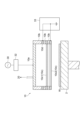
- FIG. 1 is a diagram illustrating a plasma processing apparatus according to one exemplary embodiment.
- FIG. FIG. 2 is a diagram illustrating potentials that may occur in the inner region of the plasma supply section of the plasma processing apparatus that does not include the voltage adjustment section shown in FIG. 1; 3 is a diagram showing the potential of the upper electrode that generates the potential shown in FIG. 2 that can occur in the inner region of the plasma supply section;
- FIG. FIG. 2 is a diagram showing an example of a plasma supply section and a voltage adjustment section shown in FIG. 1;
- FIG. 2 is a diagram showing an example of a plasma supply section and a voltage adjustment section shown in FIG. 1;
- FIG. 6 is a diagram illustrating potentials that may occur in the inner region of the plasma supply section electrically connected to the voltage adjustment section shown in FIGS.
- FIG. 7 is a diagram showing the potential of the upper electrode that generates the potential shown in FIG. 6 that can occur in the inner region of the plasma supply section.
- FIG. 2 is a diagram showing an example of a plasma supply section and a voltage adjustment section shown in FIG. 1; 9 is a diagram illustrating the filter circuit shown in FIG. 8.
- FIG. 9 is a diagram illustrating potentials that can occur in the inner region of the plasma supply section electrically connected to the voltage adjustment section shown in FIG. 8;
- FIG. 11 is a diagram showing the potential of the upper electrode that generates the potential shown in FIG. 10 that can occur in the inner region of the plasma supply section.
- FIG. 2 is a diagram showing an example of a plasma supply section and a voltage adjustment section shown in FIG. 1; FIG.
- FIG. 2 is a diagram showing an example of a plasma supply section and a voltage adjustment section shown in FIG. 1;
- FIG. 14 is a diagram illustrating potentials that can occur in the inner region of the plasma supply section electrically connected to the voltage adjustment section shown in FIGS. 12 and 13.
- FIG. 15 is a diagram showing the potential of the upper electrode that generates the potential shown in FIG. 14 that can occur in the inner region of the plasma supply section.
- FIG. 2 is a diagram showing an example of a plasma supply section and a voltage adjustment section shown in FIG. 1;
- the plasma supply unit that generates plasma and supplies only radicals or radicals and some ions to the process space is a remote plasma source.
- plasma is generated in the inner region of the plasma supply section 10
- a process using only radicals or radicals and some ions is performed in the outer region of the plasma supply section.
- a mesh structure that penetrates both regions and allows radicals in the plasma to pass through may be used.
- such a mesh structure may be used in a capacitively coupled plasma processing apparatus. In this case, the mesh may be damaged by the collision of ions in the plasma, and the mesh may be heated, resulting in defects in the mesh structure itself or particles generated by the defects leaking to the outside of the plasma supply section.
- a plasma processing apparatus may include a processing container, a high frequency power source, a plasma supply section, a gas supply section, and a voltage adjustment section.
- the plasma supply section includes an upper electrode and a lower electrode section, and can be configured to supply only radicals, or radicals and some ions to the processing chamber.
- the upper electrode may be configured to be electrically connected to a high frequency power source and to receive a high frequency voltage from the high frequency power source.
- the lower electrode part may be provided to face the upper electrode.
- the gas supply may be configured to supply a processing gas to the plasma supply for use in generating plasma in the plasma supply.
- the voltage adjustment unit may be used to adjust the voltage of the upper electrode.
- the space provided by the upper electrode and the lower electrode part may be configured to be supplied with a processing gas by a gas supply part.
- the lower electrode portion extends along the surface of the upper electrode and may include an electrode plate with a mesh structure.
- the mesh-structured electrode plate may be configured to communicate an inner region and an outer region of the plasma supply section provided by the lower electrode section.
- the plasma supply section and the voltage adjustment section may be configured to lower the sheath voltage of the sheath region formed on the lower electrode section during generation of plasma in the plasma supply section.
- the sheath voltage of the sheath region formed on the lower electrode section including the mesh-structured electrode during plasma generation can be reduced by the plasma supply section and the voltage adjustment section. Therefore, damage and heating to the lower electrode portion are reduced, and defects in the mesh structure itself and leakage of particles caused by the defects to the outside region of the plasma supply portion can be suppressed.
- the voltage regulator may include a diode.
- the anode of the diode may be electrically connected to the top electrode.
- the cathode of the diode may be electrically connected to ground together with the lower electrode portion.
- the voltage regulator may include a switch circuit.
- the lower electrode portion may be electrically connected to ground.
- the switch circuit may be electrically connected between the lower electrode portion and the upper electrode and configured to suppress a positive voltage component of the high frequency voltage applied to the upper electrode by the high frequency power source.
- the voltage regulator may include a diode, a filter circuit, and a DC power supply.
- the anode of the diode may be electrically connected to the top electrode.
- the filter circuit may include a first capacitor, a second capacitor, a third capacitor, and an inductor.
- the inductor and the second capacitor may be electrically connected in parallel between the diode and the DC power source.
- a cathode of the diode may be electrically connected to a negative terminal of a DC power source via an inductor and a second capacitor.
- a cathode of the diode may be electrically connected to ground via a first capacitor.
- a negative terminal of the DC power source may be electrically connected to ground via a third capacitor.
- a positive terminal of the DC power source may be electrically connected to the lower electrode portion and ground.
- the plasma supply unit may further include an electrode provided on a side wall of the plasma supply unit extending between the upper electrode and the lower electrode unit and electrically connected to ground.
- the voltage regulator may be configured to electrically connect the electrode to ground.
- the lower electrode portion may be configured to be electrically floating.
- the plasma processing apparatus further includes an electrode provided on a side wall of the plasma supply part extending between the upper electrode part and the lower electrode part and electrically connected to ground via an LC series resonant circuit.
- the voltage regulator may include an LC series resonant circuit.
- the lower electrode portion may be configured to be electrically floating.
- the plasma processing apparatus may further include an electrode provided on a side wall of the plasma supply section extending between the upper electrode and the lower electrode section and electrically connected to ground.
- the lower electrode portion may include a first electrode plate and a second electrode plate each having a mesh structure and extending in parallel to each other.
- the first electrode plate may be arranged between the second electrode plate and the upper electrode and configured to be electrically floating.
- the second electrode plate may be electrically connected to ground.
- the voltage regulator may be configured to electrically connect the electrode and the second electrode plate to ground.
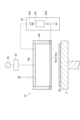
- FIG. 1 is a cross-sectional view schematically showing a plasma processing apparatus according to one exemplary embodiment.
- the plasma processing apparatus 100 performs radical processing on a process space including a substrate W, and is configured as a remote plasma processing apparatus using capacitively coupled plasma.
- the substrate W may be, for example, a semiconductor wafer, but is not limited thereto.
- the plasma processing apparatus 100 has a substantially cylindrical metal processing container 1.
- the processing container 1 is electrically connected to the ground (grounded).
- a substrate mounting table 2 for horizontally mounting a substrate W is provided inside the processing container 1 .
- the substrate mounting table 2 may have a heating mechanism or a cooling mechanism depending on the plasma processing.
- a plurality of elevating pins (not shown) are inserted into the substrate mounting table 2 so as to be able to protrude and retract from the top surface thereof, and the substrate mounting table is raised and lowered by the elevating and lowering movement of the plurality of elevating pins by an elevating mechanism (not shown).
- the substrate W is transferred to and from the terminal 2.
- the plasma processing apparatus 100 includes a gas supply section 20.
- the gas supply section 20 is configured to supply the plasma supply section 10 with a processing gas used to generate plasma in the plasma supply section 10 .
- the gas supply unit 20 can supply a plurality of gases necessary for plasma processing, such as a processing gas, a plasma generation gas, and a purge gas.
- gases necessary for plasma processing such as a processing gas, a plasma generation gas, and a purge gas.
- An appropriate processing gas can be selected depending on the plasma processing to be performed.
- the gas supply section 20 has a plurality of gas supply sources and gas supply piping, and the gas supply piping is provided with valves and a flow rate controller such as a mass flow controller.
- An exhaust port 41 is provided on the bottom wall of the processing container 1 , and an exhaust device 43 is connected to the exhaust port 41 via an exhaust pipe 42 .
- the exhaust device 43 includes an automatic pressure control valve and a vacuum pump, and is configured to evacuate the inside of the processing container 1 and maintain the inside of the processing container 1 at a desired degree of vacuum.
- the control unit 50 may include a main control unit including a CPU, an input device, an output device, a display device, and a storage device.
- the processing of the plasma processing apparatus 100 can be controlled based on the processing recipe stored in the storage medium of the storage device.
- a loading/unloading port for loading/unloading the substrate W into/out of the processing container 1 is provided on the side wall of the processing container 1, and this loading/unloading port is configured to be opened and closed by a gate valve. can be done.
- the plasma supply unit 10 is configured to supply plasma to the processing container 1.
- the plasma supply section 10 includes an upper electrode 10a and a lower electrode section 10c.
- the upper electrode 10a is configured to be electrically connected to a high frequency power source 30 and to receive a high frequency voltage from the high frequency power source 30.
- the lower electrode portion 10c is provided to face the upper electrode 10a.
- the high frequency power supply 30 can apply a high frequency voltage of 10 kHz to 60 MHz to the upper electrode 10a.
- a matching box 32 is connected to the power supply line 31 downstream of the high frequency power source 30 .
- the matching device 32 matches the load impedance to the internal (or output) impedance of the high frequency power source 30.
- the lower electrode portion 10c extends along the surface of the upper electrode 10a.
- the lower electrode section 10c includes an electrode plate 10c1.
- the electrode plate 10c1 communicates with the inner region (region where plasma is generated) and the outer region (region where processing of the substrate W is performed by plasma) of the plasma supply section 10 provided by the lower electrode section 10c. It has a structured mesh structure.
- the space provided by the upper electrode 10a and the lower electrode part 10c may be configured to be supplied with a processing gas by the gas supply part 20.
- the plasma supply section 10 is configured to generate plasma from this processing gas and supply electrically neutral radicals contained in the plasma into the processing chamber 1 via the lower electrode section 10c having a mesh structure. .
- Ions in the plasma generated in the plasma supply section 10 can be accelerated toward the lower electrode section 10c by the sheath voltage (difference between the potential of the plasma and the potential of the lower electrode section 10c) of the sheath region MS on the lower electrode section 10c. . Ions in the plasma can collide with the mesh-structured electrode plate included in the lower electrode section 10c. For this reason, the lower electrode section 10c suppresses the supply of ions to the outer region of the plasma supply section 10 through this mesh structure, and supplies (inflows) radicals in the plasma to the outer region of the plasma supply section 10. ).
- the plasma processing apparatus 100 includes a voltage adjustment section 33.
- the voltage adjustment section 33 is used to adjust the voltage of the upper electrode 10a.
- the voltage adjustment section 33, or the plasma supply section 10 and the voltage adjustment section 33 (configurations shown in FIGS. 4, 5, 8, 12, 13, and 16, respectively) are configured to control the lower electrode section 10c during plasma generation in the plasma supply section 10. It is configured to lower the voltage of the sheath region MS formed above. In this way, the voltage regulator 33 or the voltage regulator 33 and the plasma supply unit 10 reduce the sheath voltage of the sheath region MS formed on the lower electrode part 10c including the mesh-structured electrode during plasma generation. obtain.
- the plasma supply unit 10 processes some of the ions in the plasma together with radicals. It may also be supplied inside the container 1.
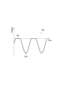
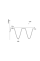
- FIG. 2 is a diagram illustrating potentials that can occur in the inner region of the plasma supply section 10 included in the plasma processing apparatus 100 in which the voltage adjustment section 33 is not provided.
- FIG. 3 is a diagram showing the potential of the upper electrode 10a that generates the potential shown in FIG. 2 that can occur in the inner region of the plasma supply section 10. Referring to FIGS. 2 and 3, this may occur when a high frequency voltage having a waveform shown in graph G1b is applied to lower electrode portion 10c by high frequency power supply 30 in plasma processing apparatus 100 in which voltage adjustment section 33 is not provided.
- a high frequency voltage is applied to the upper electrode 10a from the high frequency power supply 30, and the lower electrode portion 10c is electrically connected to ground.
- the horizontal axis of the graph G1a in FIG. 2 represents the position of the space between the upper electrode 10a and the lower electrode section 10c (referred to as the inner region of the plasma supply section 10), and the left side of the horizontal axis represents the lower electrode section. 10c, and the right side of the horizontal axis corresponds to the upper electrode 10a.
- the vertical axis of the graph G1a represents the potential that can occur in the inner region.
- the horizontal axis of the graph G1b in FIG. 3 represents time (Time), and the vertical axis of the graph G1b represents the voltage (Voltage) of the high frequency voltage applied to the lower electrode portion 10c.
- a broken line K1a represents the potential of the inner region of the plasma supply section 10 according to the positive peak (maximum value) of the high frequency voltage shown at the point P1a of the graph G1b applied to the upper electrode 10a.
- a broken line K1b of the graph G1b represents the potential of the inner region of the plasma supply unit 10 according to the negative peak (minimum value) of the high frequency voltage shown at the point P1b applied to the upper electrode 10a.
- a broken line K1c in the graph G1b represents the potential of the inner region of the plasma supply section 10 according to the zero value of the high frequency voltage shown at the point P1c applied to the upper electrode 10a.
- the sheath voltage of the sheath region MS is the maximum acceleration voltage MAV of ions in the plasma toward the lower electrode part 10c. It corresponds to A sheath region SS is formed below the upper electrode 10a in the inner region of the plasma supply section 10.
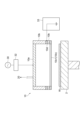
- FIGS. 4 and 5 A plasma supply section 10 and voltage adjustment section 33 of a plasma processing apparatus 100 according to one exemplary embodiment are shown in FIGS. 4 and 5.
- the voltage adjustment section 33 shown in FIG. 4 is configured to suppress the positive voltage component of the high frequency voltage applied to the upper electrode 10a by the high frequency power supply 30. It includes a diode 33a. The anode of the diode 33a is electrically connected to the upper electrode 10a. The cathode of the diode 33a is electrically connected to the ground together with the lower electrode portion 10c.
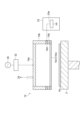
- the voltage adjustment unit 33 shown in FIG. 5 is also configured to suppress the positive voltage component of the high frequency voltage applied to the upper electrode 10a by the high frequency power supply 30.
- the voltage regulator 33 shown in FIG. 5 includes a switch circuit 33b.
- the lower electrode portion 10c shown in FIG. 5 is electrically connected to ground.
- the switch circuit 33b is electrically connected between the lower electrode portion 10c and the upper electrode 10a.
- the maximum acceleration voltage MAV sheath voltage of the sheath region MS
- the maximum acceleration voltage MAV shown in graph G1a of FIG. is lower than the maximum acceleration voltage MAV shown in graph G1a of FIG. Therefore, the acceleration of ions in the plasma toward the lower electrode section 10c is reduced compared to the case where the voltage adjustment section 33 is not provided, and damage caused by ion collisions that the lower electrode section 10c may receive can also be reduced.
- the lower electrode portion 10c shown in FIGS. 4 and 5 is composed of a single electrode plate 10c1 having a mesh structure.
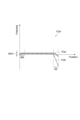
- FIG. 6 is a diagram illustrating potentials that can occur in the inner region of the plasma supply section 10 shown in FIGS. 4 and 5.
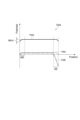
- FIG. 7 is a diagram showing the potential of the upper electrode 10a that generates the potential shown in FIG. 6 that can occur in the inner region of the plasma supply section 10. 6 and 7, the potential that can be generated in the inner region of the plasma supply unit 10 corresponding to the peak (maximum value) of the high frequency voltage shown at point P2a of graph G2b applied to upper electrode 10a is expressed by broken line K2a of graph G2a.
- the potential generated in the inner region of the plasma supply unit 10 corresponding to the peak (minimum value) of the high frequency voltage shown at point P2b of graph G2b applied to upper electrode 10a is represented by broken line K2b of graph G2a.
- the voltage adjustment section 33 shown in FIGS. 4 and 5 applies a voltage having the waveform of the graph G2b shown in FIG. 7, in which the positive voltage component of the high frequency voltage output from the high frequency power source 30 is suppressed, to the upper electrode 10a.
- Ru Since the positive voltage component of the high frequency voltage is suppressed, the maximum acceleration voltage MAV corresponding to the sheath voltage of the sheath region MS is equal to the maximum acceleration voltage MAV shown in the graph G1a of FIG. 2 when the voltage adjustment section 33 is not provided. suppressed in comparison. Therefore, damage caused by ion collisions that may be caused to the lower electrode portion 10c can also be suppressed.
- FIGS. 8 and 9 A plasma supply section 10 and voltage adjustment section 33 of a plasma processing apparatus 100 according to one exemplary embodiment are shown in FIGS. 8 and 9.
- the voltage adjustment section 33 shown in FIG. 8 is configured to suppress the positive voltage component of the high frequency voltage applied to the upper electrode 10a by the high frequency power supply 30.
- the voltage regulator 33 shown in FIG. 8 includes a diode 33a, a filter circuit 33c, and a DC power supply 33d.
- the anode of the diode 33a is electrically connected to the upper electrode 10a.
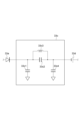
- the filter circuit 33c includes a capacitor 33c1, a capacitor 33c2, a capacitor 33c4, and an inductor 33c3.
- the inductor 33c3 and the capacitor 33c2 are electrically connected in parallel between the diode 33a and the DC power supply 33d.
- the cathode of the diode 33a is electrically connected to the negative terminal of the DC power supply 33d via an inductor 33c3 and a capacitor 33c2.
- a cathode of the diode 33a is electrically connected to ground via a capacitor 33c1.
- a negative terminal of the DC power supply 33d is electrically connected to ground via a capacitor 33c4.
- a positive terminal of the DC power supply 33d is electrically connected to the lower electrode portion 10c and the ground.
- the maximum acceleration voltage MAV sheath voltage of the sheath region MS shown in the graph G3a of FIG. 10 is as follows. It is lower than the maximum acceleration voltage MAV shown in graph G1a of FIG. Therefore, the acceleration of ions in the plasma toward the lower electrode section 10c is reduced compared to the case where the voltage adjustment section 33 is not provided, and damage caused by ion collisions that the lower electrode section 10c may receive can also be reduced.
- the lower electrode portion 10c shown in FIG. 8 is composed of one electrode plate 10c1 having a mesh structure.
- FIG. 10 is a diagram illustrating potentials that can occur in the inner region of the plasma supply section 10 shown in FIGS. 8 and 9.
- FIG. 11 is a diagram showing the potential of the upper electrode 10a that generates the potential shown in FIG. 10 that may occur in the inner region of the plasma supply section 10.
- the potential generated in the inner region of the plasma supply unit 10 corresponding to the peak (maximum value) of the high-frequency voltage shown at point P3a of graph G3b applied to upper electrode 10a is expressed by broken line K3a of graph G3a.
- the potential generated in the inner region of the plasma supply section 10 corresponding to the peak (minimum value) of the high frequency voltage shown at point P3b of graph G3b applied to upper electrode 10a is represented by broken line K3b of graph G3a.
- the voltage adjustment unit 33 shown in FIGS. 8 and 9 the voltage having the waveform of the graph G3b shown in FIG. is applied to Therefore, the maximum acceleration voltage MAV corresponding to the sheath voltage of the sheath region MS is suppressed compared to the maximum acceleration voltage MAV shown in the graph G1a of FIG. 2 when the voltage adjustment section 33 is not provided. Therefore, damage caused by ion collisions that the lower electrode portion 10c may receive can also be suppressed.
- FIGS. 12 and 13 A plasma supply section 10 and voltage adjustment section 33 of a plasma processing apparatus 100 according to one exemplary embodiment are shown in FIGS. 12 and 13.
- the plasma processing apparatus 100 having the plasma supply section 10 shown in FIG. 12 further includes an electrode 10d.
- This electrode 10d is provided on the side wall 10b of the plasma supply section 10 extending between the upper electrode 10a and the lower electrode section 10c.
- the electrode 10d is electrically connected to the ground (voltage adjustment section 33).
- the voltage regulator 33 shown in FIG. 12 is configured to electrically connect the electrode 10d to ground.
- the lower electrode portion 10c shown in FIG. 12 is configured to be in an electrically floating state. In this way, the lower electrode portion 10c is in an electrically floating state. Therefore, since the potential of the lower electrode portion 10c can change following the plasma potential, the maximum acceleration voltage MAV corresponding to the sheath voltage remains low.
- the maximum acceleration voltage MAV corresponding to the sheath voltage of the sheath region MS can be suppressed compared to the maximum acceleration voltage MAV shown in the graph G1a of FIG. 2 when the voltage adjustment section 33 is not provided. Therefore, damage caused to the lower electrode portion 10c by ion collisions can be sufficiently reduced.
- the plasma processing apparatus 100 having the plasma supply section 10 shown in FIG. 13 further includes an electrode 10d.
- the electrode 10d is provided on the side wall 10b of the plasma supply section 10 extending between the upper electrode 10a and the lower electrode section 10c.
- the voltage regulator 33 shown in FIG. 13 includes an LC series resonant circuit 33e.
- the voltage adjustment unit 33 is configured to electrically connect the electrode 10d to the ground via the LC series resonant circuit 33e.
- the electrode 10d is electrically connected to ground via the LC series resonant circuit 33e.
- the lower electrode portion 10c shown in FIG. 13 is configured to be in an electrically floating state. In this way, the lower electrode portion 10c is in an electrically floating state.
- the maximum acceleration voltage MAV corresponding to the sheath voltage remains low. Therefore, the maximum acceleration voltage MAV corresponding to the sheath voltage of the sheath region MS can be suppressed compared to the maximum acceleration voltage MAV shown in the graph G1a of FIG. 2 when the voltage adjustment section 33 is not provided. Therefore, damage to the lower electrode portion 10c due to ion collisions can be sufficiently reduced.
- the maximum acceleration voltage MAV shown in the graph G4a of FIG. 14 is the maximum acceleration voltage MAV shown in the graph G1a of FIG. Lower than acceleration voltage MAV. Therefore, the acceleration of ions in the plasma toward the lower electrode section 10c is reduced compared to the case where the voltage adjustment section 33 is not provided, and damage caused by ion collisions that the lower electrode section 10c may receive can also be reduced.
- the lower electrode portion 10c shown in FIGS. 12 and 13 is composed of a single electrode plate 10c1 having a mesh structure.
- FIG. 14 is a diagram illustrating potentials that can occur in the inner region of the plasma supply section 10 shown in FIGS. 12 and 13.
- FIG. 15 is a diagram showing the potential of the upper electrode 10a that generates the potential shown in FIG. 14 that may occur in the inner region of the plasma supply section 10.
- the potential generated in the inner region of the plasma supply unit 10 corresponding to the peak (maximum value) of the high frequency voltage shown at point P4a of graph G4b applied to upper electrode 10a is expressed by broken line K4a of graph G4a.
- the potential that can be generated in the inner region of the plasma supply section 10 corresponding to the peak (minimum value) of the high frequency voltage shown at the point P4b applied to the upper electrode 10a is represented by the broken line K4b of the graph G4a.
- the potential that can be generated in the inner region of the plasma supply section 10 corresponding to the zero value of the high frequency voltage shown at the point P4c applied to the upper electrode 10a is represented by the broken line K4c of the graph G4a.
- the potential of the lower electrode portion 10c is , can change following fluctuations in plasma potential.
- the maximum acceleration voltage MAV corresponding to the sheath voltage of the sheath region MS is suppressed compared to the maximum acceleration voltage MAV shown in the graph G1a of FIG. 2 when the voltage adjustment section 33 is not provided. Therefore, damage caused by ion collisions that the lower electrode portion 10c may receive can also be suppressed.
- the plasma supply section 10 and voltage adjustment section 33 of the plasma processing apparatus 100 are shown in FIG. 16.
- the plasma supply section 10 shown in FIG. 16 is further provided with an electrode plate 10c2 in addition to the configuration of the plasma supply section 10 shown in FIG. 12. That is, the lower electrode portion 10c includes an electrode plate 10c1 and an electrode plate 10c2, each having a mesh structure and extending parallel to each other.
- the electrode plate 10c1 is arranged between the upper electrode 10a and the electrode plate 10c2, and is configured to be in an electrically floating state.
- the electrode plate 10c2 is electrically connected to the ground (voltage adjustment section 33).
- the voltage adjustment unit 33 shown in FIG. 16 is configured to electrically connect the electrode 10d and the electrode plate 10c2 to the ground.
- the maximum acceleration voltage MAV (sheath voltage of the sheath region MS) in the plasma processing apparatus 100 in which the lower electrode section 10c and the voltage adjustment section 33 shown in FIG. 16 are provided is the maximum acceleration voltage shown in the graph G4a of FIG. 14. It is similar to MAV. Therefore, the acceleration of ions in the plasma toward the lower electrode section 10c is reduced compared to the case where the voltage adjustment section 33 is not provided, and damage caused by ion collisions that the lower electrode section 10c may receive can also be reduced. That is, at least the same effect as that achieved by the configuration of FIG. 12 can also be achieved by the configuration of FIG. 16. Furthermore, since the electrode plate 10c2 is provided in the configuration of FIG.
- SYMBOLS 1 Processing container, 10... Plasma supply part, 10a... Upper electrode, 10c... Lower electrode part, 10c1... Electrode plate, 10c2... Electrode plate, 10d... Electrode, 100... Plasma processing apparatus, 20... Gas supply part, 30... High frequency power supply, 33... Voltage adjustment section, 33a... Diode, 33b... Switch circuit, 33c... Filter circuit, 33c1... Capacitor, 33c2... Capacitor, 33c3... Inductor, 33c4... Capacitor, 33d... DC power supply, 33e... LC series resonant circuit .
Landscapes
- Physics & Mathematics (AREA)
- Engineering & Computer Science (AREA)
- Plasma & Fusion (AREA)
- Chemical & Material Sciences (AREA)
- Analytical Chemistry (AREA)
- Electromagnetism (AREA)
- Spectroscopy & Molecular Physics (AREA)
- Drying Of Semiconductors (AREA)
- Plasma Technology (AREA)
- Chemical Vapour Deposition (AREA)
Abstract
リモートプラズマ源がプラズマによって受け得る影響を低減する一つの例示的実施形態においてプラズマ処理装置が提供される。プラズマ供給部は上部電極及び下部電極部を含み処理容器にラジカルのみ、又はラジカル及び一部のイオンを供給するように構成され、上部電極は高周波電源から高周波電圧が印加されるように構成され、電圧調整部は上部電圧の電圧の調整に用いられ、下部電極部は上部電極に対向するように設けられ上部電極の表面に沿って拡がっておりメッシュ構造の電極板を含み、メッシュ構造の電極板は下部電極部によって提供されるプラズマ供給部の内領域及び外領域を連通するように構成され、プラズマ供給部及び電圧調整部はプラズマ供給部におけるプラズマの生成中に下部電極部上に形成されるシース領域のシース電圧を下げるように構成される。
Description
本開示の例示的実施形態は、プラズマ処理装置に関するものである。
半導体ウエハ等の基板に対する処理としてプラズマ処理が多用されている。プラズマ処理にはプラズマ処理装置が用いられ、例えばリモートプラズマ源によってプラズマが提供され得る。特許文献1~4には、リモートプラズマ源を有するプラズマ処理装置に係る技術が開示されている。
本開示は、リモートプラズマ源がプラズマによって受け得る影響を低減する技術を提供する。
一つの例示的実施形態において、プラズマ処理装置が提供される。プラズマ処理装置は、処理容器と、高周波電源とプラズマ供給部とガス供給部と電圧調整部とを備え得る。プラズマ供給部は、上部電極及び下部電極部を含み、処理容器にラジカルのみ、又はラジカル及び一部のイオンを供給するように構成され得る。上部電極は、高周波電源に電気的に接続され高周波電源から高周波電圧が印加されるように構成され得る。下部電極部は、上部電極に対向するように設けられ得る。ガス供給部は、プラズマ供給部におけるプラズマの生成に用いる処理ガスをプラズマ供給部に供給するように構成され得る。電圧調整部は、上部電極の電圧の調整に用いられ得る。上部電極及び下部電極部によって提供される空間は、ガス供給部によって処理ガスが供給されるように構成され得る。下部電極部は、上部電極の表面に沿って拡がっており、メッシュ構造の電極板を含み得る。メッシュ構造の電極板は、下部電極部によって提供されるプラズマ供給部の内領域及び外領域を連通するように構成され得る。プラズマ供給部及び電圧調整部は、プラズマ供給部におけるプラズマの生成中に下部電極部上に形成されるシース領域のシース電圧を下げるように構成され得る。
一つの例示的実施形態によれば、リモートプラズマ源がプラズマによって受け得る影響を低減するための技術が提供される。
以下、種々の例示的実施形態について説明する。
プラズマを生成しプロセス空間にラジカルのみ、又はラジカル及び一部のイオンを供給するプラズマ供給部がリモートプラズマ源の場合を考える。この場合、プラズマ供給部10の内領域ではプラズマが生成され、プラズマ供給部の外領域ではラジカルのみ、又はラジカル及び一部のイオンによるプロセス処理が行われる。プラズマ供給部の内領域及び外領域の画定に(両領域を仕切る手段として)、両領域を貫通しプラズマ中のラジカルの通過を可能とするメッシュ構造が用いられる場合があり得る。更に、容量結合型のプラズマ処理装置にこのようなメッシュ構造が用いられる場合があり得る。この場合、プラズマ中のイオンの衝突によってメッシュにダメージが生じ、メッシュが加熱されて、メッシュ構造自体の欠損や、欠損によって生じるパーティクルがプラズマ供給部の外領域に漏出する現象が生じ得る。
一つの例示的実施形態において、プラズマ処理装置が提供される。プラズマ処理装置は、処理容器と、高周波電源とプラズマ供給部とガス供給部と電圧調整部とを備え得る。プラズマ供給部は、上部電極及び下部電極部を含み、処理容器にラジカルのみ、又ははラジカル及び一部のイオンを供給するように構成され得る。上部電極は、高周波電源に電気的に接続され高周波電源から高周波電圧が印加されるように構成され得る。下部電極部は、上部電極に対向するように設けられ得る。ガス供給部は、プラズマ供給部におけるプラズマの生成に用いる処理ガスをプラズマ供給部に供給するように構成され得る。電圧調整部は、上部電極の電圧の調整に用いられ得る。上部電極及び下部電極部によって提供される空間は、ガス供給部によって処理ガスが供給されるように構成され得る。下部電極部は、上部電極の表面に沿って拡がっており、メッシュ構造の電極板を含み得る。メッシュ構造の電極板は、下部電極部によって提供されるプラズマ供給部の内領域及び外領域を連通するように構成され得る。プラズマ供給部及び電圧調整部は、プラズマ供給部におけるプラズマの生成中に下部電極部上に形成されるシース領域のシース電圧を下げるように構成され得る。
このように、プラズマ供給部や電圧調整部によって、プラズマの生成中にメッシュ構造の電極を含む下部電極部上に形成されるシース領域のシース電圧が低減され得る。したがって、下部電極部へのダメージ及び加熱が低減され、メッシュ構造自体の欠損や、欠損によって生じるパーティクルがプラズマ供給部の外領域に漏出する現象が抑制され得る。
一つの例示的実施形態において、電圧調整部は、ダイオードを含み得る。ダイオードのアノードは、上部電極に電気的に接続され得る。ダイオードのカソードは、下部電極部と共にグランドに電気的に接続され得る。
一つの例示的実施形態において、電圧調整部は、スイッチ回路を含み得る。下部電極部は、グランドに電気的に接続され得る。スイッチ回路は、下部電極部及び上部電極の間に電気的に接続され、高周波電源によって上部電極に印加される高周波電圧の正電圧成分を抑制するように構成され得る。
一つの例示的実施形態において、電圧調整部は、ダイオード、フィルタ回路、及び直流電源を含み得る。ダイオードのアノードは、上部電極に電気的に接続され得る。フィルタ回路は、第1のキャパシタ、第2のキャパシタ、第3のキャパシタ、及びインダクタを含み得る。インダクタ及び第2のキャパシタは、ダイオード及び直流電源の間において電気的に並列接続され得る。ダイオードのカソードは、インダクタ及び第2のキャパシタを介して直流電源のマイナス端子に電気的に接続され得る。ダイオードのカソードは、第1のキャパシタを介してグランドに電気的に接続され得る。直流電源のマイナス端子は、第3のキャパシタを介してグランドに電気的に接続され得る。直流電源のプラス端子は、下部電極部及びグランドに電気的に接続され得る。
一つの例示的実施形態において、上部電極及び下部電極部の間に延びるプラズマ供給部の側壁に設けられ、グランドに電気的に接続された電極を更に備え得る。電圧調整部は、電極をグランドに電気的に接続するように構成され得る。下部電極部は、電気的にフローティング状態となるように構成され得る。
一つの例示的実施形態において、プラズマ処理装置は、上部電極及び下部電極部の間に延びるプラズマ供給部の側壁に設けられ、LC直列共振回路を介してグランドに電気的に接続された電極を更に備え得る。電圧調整部は、LC直列共振回路を含み得る。下部電極部は、電気的にフローティング状態となるように構成され得る。
一つの例示的実施形態において、プラズマ処理装置は、上部電極及び下部電極部の間に延びるプラズマ供給部の側壁に設けられ、グランドに電気的に接続された電極を更に備え得る。下部電極部は、それぞれメッシュ構造を有し互いに平行に延びる第1の電極板及び第2の電極板を含み得る。第1の電極板は、第2の電極板及び上部電極の間に配置され、電気的にフローティング状態となるように構成され得る。第2の電極板は、グランドに電気的に接続され得る。電圧調整部は、電極及び第2の電極板をグランドに電気的に接続するように構成され得る。
以下、図面を参照して種々の例示的実施形態について詳細に説明する。なお、各図面において同一又は相当の部分に対しては同一の符号を附すこととする。
図1は、一つの例示的実施形態に係るプラズマ処理装置を概略的に示す断面図である。プラズマ処理装置100は、基板Wを含むプロセス空間に対してラジカル処理を行うものであり、容量結合プラズマを用いたリモートプラズマ処理装置として構成されている。基板Wとしては、例えば半導体ウエハを挙げることができるが、これに限定されない。
プラズマ処理装置100は、略円筒状の金属製の処理容器1を有している。処理容器1は、グランドに電気的に接続(接地)されている。処理容器1の内部には、基板Wを水平に載置するための基板載置台2が設けられている。
基板載置台2には、プラズマ処理に応じて、加熱機構または冷却機構を有していてもよい。基板載置台2には、その上面に対し突没可能に複数の昇降ピン(図示せず)が挿通されており、昇降機構(図示せず)による複数の昇降ピンの昇降動作により、基板載置台2に対する基板Wの授受が行われるようになっている。
プラズマ処理装置100は、ガス供給部20を備える。ガス供給部20は、プラズマ供給部10におけるプラズマの生成に用いる処理ガスをプラズマ供給部10に供給するように構成されている。
ガス供給部20は、プラズマ処理に必要な処理ガス、プラズマ生成ガス、パージガス等の複数のガスを供給し得る。処理ガスとしては、実施されるプラズマ処理に応じて適切なものが選択され得る。ガス供給部20は、複数のガス供給源およびガス供給配管を有し、ガス供給配管には、バルブ類およびマスフローコントローラのような流量制御器が設けられている。
処理容器1の底壁には排気口41が設けられており、排気口41には排気管42を介して排気装置43が接続されている。排気装置43は、自動圧力制御バルブ及び真空ポンプを含み、排気装置43によって処理容器1内を排気するとともに、処理容器1内を所望の真空度に保持できるように構成されている。
ガス供給部20のバルブ類及び流量制御器、並びに高周波電源30等のプラズマ処理装置100の各部は、制御部50によって制御され得る。制御部50は、CPUを有する主制御部と、入力装置、出力装置、表示装置、および記憶装置とを有し得る。記憶装置の記憶媒体に記憶された処理レシピに基づいてプラズマ処理装置100の処理が制御され得る。
なお、図示していないが、処理容器1の側壁には、処理容器1に対して基板Wを搬入出するための搬入出口が設けられており、この搬入出口はゲートバルブで開閉するように構成され得る。
処理容器1の上部には、開口が形成されており、開口には絶縁部材9を介してプラズマ供給部10が基板載置台2に対向するように嵌め込まれている。プラズマ供給部10は、処理容器1にプラズマを供給するように構成されている。プラズマ供給部10は、上部電極10a及び下部電極部10cを含んでいる。
上部電極10aは、高周波電源30に電気的に接続され高周波電源30から高周波電圧が印加されるように構成されている。下部電極部10cは、上部電極10aに対向するように設けられている。高周波電源30は、10kHz~60MHzの高周波電圧を上部電極10aに印加し得る。給電ライン31の高周波電源30下流側には整合器32が接続されている。整合器32は高周波電源30の内部(または出力)インピーダンスに負荷インピーダンスを整合させるものである。
下部電極部10cは、上部電極10aの表面に沿って拡がっている。下部電極部10cは、電極板10c1を含む。電極板10c1は、下部電極部10cによって提供されるプラズマ供給部10の内領域(プラズマが生成される領域)及び外領域(プラズマによる基板Wへのプロセス処理が行われる領域)を連通するように構成されたメッシュ構造を有する。上部電極10a及び下部電極部10cによって提供される空間は、ガス供給部20によって処理ガスが供給されるように構成され得る。プラズマ供給部10は、この処理ガスからプラズマを生成し、プラズマに含まれる電気的に中性なラジカルをメッシュ構造の下部電極部10cを介して処理容器1内に供給するように構成されている。
プラズマ供給部10において生成されるプラズマ中のイオンは下部電極部10c上のシース領域MSのシース電圧(プラズマの電位及び下部電極部10cの電位の差分)で下部電極部10cに向けて加速され得る。プラズマ中のイオンは、下部電極部10cに含まれるメッシュ構造の電極板に衝突し得る。このため、下部電極部10cは、このメッシュ構造によって、プラズマ供給部10の外領域へのイオンの供給を抑制するとともに、プラズマ中のラジカルをプラズマ供給部10の外領域に供給する(流入させ得る)。
プラズマ処理装置100は、電圧調整部33を備える。電圧調整部33は、上部電極10aの電圧の調整に用いられる。電圧調整部33、又はプラズマ供給部10及び電圧調整部33(図4、5、8、12、13、16のそれぞれに示す構成)は、プラズマ供給部10におけるプラズマの生成中に下部電極部10c上に形成されるシース領域MSの電圧を下げるように構成されている。このように、電圧調整部33、又は電圧調整部33及びプラズマ供給部10によって、プラズマの生成中にメッシュ構造の電極を含む下部電極部10c上に形成されるシース領域MSのシース電圧が低減され得る。したがって、下部電極部10cへのダメージ及び加熱が低減され、メッシュ構造自体の欠損や、欠損によって生じるパーティクルがプラズマ供給部10の外領域に漏出する現象が抑制され得る。尚、プラズマ供給部10から処理容器1の内側に供給するものをラジカルとして説明したが、基板Wのプロセス処理を向上する目的で、プラズマ供給部10はプラズマ中のイオンの一部をラジカルと共に処理容器1の内側に供給しても良い。
図2は、電圧調整部33が設けられていないプラズマ処理装置100に含まれるプラズマ供給部10の内領域において生じ得る電位を例示する図である。図3は、プラズマ供給部10の内領域において生じ得る図2に示す電位を発生させる上部電極10aの電位を示す図である。図2及び図3を参照して、電圧調整部33が設けられていないプラズマ処理装置100において、高周波電源30によってグラフG1bに示す波形の高周波電圧が下部電極部10cに印加される場合に生じ得るシース領域MSのシース電圧を考える。この場合、上部電極10aには高周波電源30から高周波電圧が印加され、下部電極部10cはグランドに電気的に接続されている。
図2のグラフG1aの横軸は、上部電極10a及び下部電極部10cの間の空間(プラズマ供給部10の内領域という)の位置(Position)を表しており、横軸の左側は下部電極部10cに対応し、横軸の右側は上部電極10aに対応している。グラフG1aの縦軸は、内領域で生じ得る電位(Potential)を表している。図3のグラフG1bの横軸は、時間(Time)を表しており、グラフG1bの縦軸は、下部電極部10cに印加される高周波電圧の電圧(Voltage)を表している。図6のグラフG2a及び図7のグラフG2bの横軸及び縦軸は、図2のグラフG1a及び図3のグラフG1bの横軸及び縦軸と同様である。更に、図10のグラフG3a及び図11のグラフG3bの横軸及び縦軸も、図2のグラフG1a及び図3のグラフG1bの横軸及び縦軸と同様である。更に、図14のグラフG4a及び図15のグラフG4bの横軸及び縦軸も、図2のグラフG1a及び図3のグラフG1bの横軸及び縦軸と同様である。
プラズマ供給部10の内領域では、グラフG1aに示す折線K1a、折線K1b、及び折線K1cのそれぞれによって表される電位(Potential)が生じ得る。折線K1aは、上部電極10aに印加されるグラフG1bのポイントP1aに示す高周波電圧の正のピーク(最大値)に応じたプラズマ供給部10の内領域の電位を表している。グラフG1bの折線K1bは、上部電極10aに印加されるポイントP1bに示す高周波電圧の負のピーク(最小値)に応じたプラズマ供給部10の内領域の電位を表している。グラフG1bの折線K1cは、上部電極10aに印加されるポイントP1cに示す高周波電圧のゼロ値に応じたプラズマ供給部10の内領域の電位を表している。
高周波電圧の正のピーク(ポイントP1a)に対応した内領域に生じ得る電位(折線K1a)のうち、シース領域MSのシース電圧は、下部電極部10cに向けたプラズマ中のイオンの最大加速電圧MAVに対応している。プラズマ供給部10の内領域における上部電極10a下には、シース領域SSが形成される。
一つの例示的実施形態に係るプラズマ処理装置100のプラズマ供給部10及び電圧調整部33が図4及び図5に示されている。
図4に示す電圧調整部33は、高周波電源30によって上部電極10aに印加される高周波電圧の正電圧成分を抑制するように構成されている。ダイオード33aを含む。ダイオード33aのアノードは、上部電極10aに電気的に接続されている。ダイオード33aのカソードは、下部電極部10cと共にグランドに電気的に接続されている。
図5に示す電圧調整部33も、高周波電源30によって上部電極10aに印加される高周波電圧の正電圧成分を抑制するように構成されている。図5に示す電圧調整部33は、スイッチ回路33bを含む。図5に示す下部電極部10cは、グランドに電気的に接続されている。スイッチ回路33bは、下部電極部10c及び上部電極10aの間に電気的に接続されている。
このような図4又は図5に示す下部電極部10c及び電圧調整部33が設けられているプラズマ処理装置100において、図6のグラフG2aに示す最大加速電圧MAV(シース領域MSのシース電圧)は、図2のグラフG1aに示す最大加速電圧MAVよりも低い。このため、下部電極部10cに向けたプラズマ中のイオンの加速が、電圧調整部33が設けられていない場合よりも低減され、下部電極部10cが受け得るイオン衝突によるダメージも低減され得る。図4及び図5に示す下部電極部10cは、メッシュ構造の一枚の電極板10c1によって構成されている。
図6は、図4及び図5に示すプラズマ供給部10の内領域において生じ得る電位を例示する図である。図7は、プラズマ供給部10の内領域において生じ得る図6に示す電位を発生させる上部電極10aの電位を示す図である。図6及び図7において、上部電極10aに印加されるグラフG2bのポイントP2aに示す高周波電圧のピーク(最大値)に対応したプラズマ供給部10の内領域に生じ得る電位は、グラフG2aの折線K2aによって表される。上部電極10aに印加されるグラフG2bのポイントP2bに示す高周波電圧のピーク(最小値)に対応したプラズマ供給部10の内領域に生じ得る電位は、グラフG2aの折線K2bによって表される。このように図4及び図5に示す電圧調整部33によって、高周波電源30から出力される高周波電圧の正電圧成分が抑制された図7に示すグラフG2bの波形の電圧が上部電極10aに印加される。高周波電圧の正電圧成分が抑制されるので、シース領域MSのシース電圧に対応する最大加速電圧MAVは、電圧調整部33が設けられていない場合の図2のグラフG1aに示す最大加速電圧MAVに比較して抑制される。よって、下部電極部10cが受け得るイオン衝突によるダメージも抑制され得る。
一つの例示的実施形態に係るプラズマ処理装置100のプラズマ供給部10及び電圧調整部33が図8及び図9に示されている。
図8に示す電圧調整部33は、高周波電源30によって上部電極10aに印加される高周波電圧の正電圧成分を抑制するように構成されている。図8に示す電圧調整部33は、ダイオード33a、フィルタ回路33c、及び直流電源33dを含む。ダイオード33aのアノードは、上部電極10aに電気的に接続されている。
フィルタ回路33cは、図9に示すように、キャパシタ33c1、キャパシタ33c2、キャパシタ33c4、及びインダクタ33c3を含む。インダクタ33c3及びキャパシタ33c2は、ダイオード33a及び直流電源33dの間において電気的に並列接続されている。ダイオード33aのカソードは、インダクタ33c3及びキャパシタ33c2を介して直流電源33dのマイナス端子に電気的に接続されている。ダイオード33aのカソードは、キャパシタ33c1を介してグランドに電気的に接続されている。直流電源33dのマイナス端子は、キャパシタ33c4を介してグランドに電気的に接続されている。直流電源33dのプラス端子は、下部電極部10c及びグランドに電気的に接続されている。
このような図8及び図9に示す下部電極部10c及び電圧調整部33が設けられているプラズマ処理装置100において図10のグラフG3aに示す最大加速電圧MAV(シース領域MSのシース電圧)は、図2のグラフG1aに示す最大加速電圧MAVよりも低い。このため、下部電極部10cに向けたプラズマ中のイオンの加速が、電圧調整部33が設けられていない場合よりも低減され、下部電極部10cが受け得るイオン衝突によるダメージも低減され得る。図8に示す下部電極部10cは、メッシュ構造の一枚の電極板10c1によって構成されている。
図10は、図8及び図9に示すプラズマ供給部10の内領域において生じ得る電位を例示する図である。図11は、プラズマ供給部10の内領域において生じ得る図10に示す電位を発生させる上部電極10aの電位を示す図である。図10及び図11において、上部電極10aに印加されるグラフG3bのポイントP3aに示す高周波電圧のピーク(最大値)に対応したプラズマ供給部10の内領域に生じ得る電位は、グラフG3aの折線K3aによって表される。上部電極10aに印加されるグラフG3bのポイントP3bに示す高周波電圧のピーク(最小値)に対応したプラズマ供給部10の内領域に生じ得る電位は、グラフG3aの折線K3bによって表される。このように図8及び図9に示す電圧調整部33によって、高周波電源30から出力される高周波電圧の正電圧成分が十分に抑制された図11に示すグラフG3bの波形の電圧が、上部電極10aに印加される。したがって、シース領域MSのシース電圧に対応する最大加速電圧MAVは、電圧調整部33が設けられていない場合の図2のグラフG1aに示す最大加速電圧MAVに比較して抑制される。よって、下部電極部10cが受け得るイオン衝突によるダメージも抑制され得る。
一つの例示的実施形態に係るプラズマ処理装置100のプラズマ供給部10及び電圧調整部33が図12及び図13に示されている。
図12に示すプラズマ供給部10を有するプラズマ処理装置100は、電極10dを更に含む。この電極10dは、上部電極10a及び下部電極部10cの間に延びるプラズマ供給部10の側壁10bに設けられている。電極10dは、グランド(電圧調整部33)に電気的に接続されている。図12に示す電圧調整部33は、電極10dをグランドに電気的に接続するように構成されている。図12に示す下部電極部10cは、電気的にフローティング状態となるように構成されている。このように、下部電極部10cが電気的にフローティング状態となっている。従って、下部電極部10cの電位はプラズマ電位に対し追従して変化し得るため、シース電圧に対応する最大加速電圧MAVは低い状態を維持する。このため、シース領域MSのシース電圧に対応する最大加速電圧MAVは、電圧調整部33が設けられていない場合の図2のグラフG1aに示す最大加速電圧MAVに比較して抑制され得る。従って、下部電極部10cが受けるイオン衝突によるダメージも十分に低減され得る。
図13に示すプラズマ供給部10を有するプラズマ処理装置100は、電極10dを更に含む。電極10dは、上部電極10a及び下部電極部10cの間に延びるプラズマ供給部10の側壁10bに設けられている。図13に示す電圧調整部33は、LC直列共振回路33eを含む。電圧調整部33は、電極10dをLC直列共振回路33eを介してグランドに電気的に接続するように構成されている。電極10dは、LC直列共振回路33eを介してグランドに電気的に接続されている。図13に示す下部電極部10cは、電気的にフローティング状態となるように構成されている。このように、下部電極部10cが電気的にフローティング状態となっている。従って、下部電極部10cの電位はプラズマ電位に対し追従して変化し得るため、シース電圧に対応する最大加速電圧MAVは低い状態を維持する。このため、シース領域MSのシース電圧に対応する最大加速電圧MAVは、電圧調整部33が設けられていない場合の図2のグラフG1aに示す最大加速電圧MAVに比較して抑制され得る。従って、下部電極部10cが受けるイオン衝突によるダメージも十分に低減され得る。
このような図12又は図13に示す下部電極部10c及び電圧調整部33が設けられているプラズマ処理装置100において図14のグラフG4aに示す最大加速電圧MAVは、図2のグラフG1aに示す最大加速電圧MAVよりも低い。このため、下部電極部10cに向けたプラズマ中のイオンの加速が、電圧調整部33が設けられていない場合よりも低減され、下部電極部10cが受け得るイオン衝突によるダメージも低減され得る。図12及び図13に示す下部電極部10cは、メッシュ構造の一枚の電極板10c1によって構成されている。
図14は、図12及び図13に示すプラズマ供給部10の内領域において生じ得る電位を例示する図である。図15は、プラズマ供給部10の内領域において生じ得る図14に示す電位を発生させる上部電極10aの電位を示す図である。図14及び図15において、上部電極10aに印加されるグラフG4bのポイントP4aに示す高周波電圧のピーク(最大値)に対応したプラズマ供給部10の内領域に生じ得る電位は、グラフG4aの折線K4aによって表される。上部電極10aに印加されるポイントP4bに示す高周波電圧のピーク(最小値)に対応したプラズマ供給部10の内領域に生じ得る電位は、グラフG4aの折線K4bによって表される。上部電極10aに印加されるポイントP4cに示す高周波電圧のゼロ値に対応したプラズマ供給部10の内領域に生じ得る電位は、グラフG4aの折線K4cによって表される。このような図14のグラフG4a及び図15のグラフG4bに示されるように、図12及び図13に示す下部電極部10cが電気的にフローティング状態となっているので、下部電極部10cの電位は、プラズマ電位の変動に追随して変化し得る。このため、シース領域MSのシース電圧に対応する最大加速電圧MAVは、電圧調整部33が設けられていない場合の図2のグラフG1aに示す最大加速電圧MAVに比較して抑制される。よって、下部電極部10cが受け得るイオン衝突によるダメージも抑制され得る。
一つの例示的実施形態に係るプラズマ処理装置100のプラズマ供給部10及び電圧調整部33が図16に示されている。
図16に示すプラズマ供給部10は、図12に示すプラズマ供給部10の構成に対して追加的に電極板10c2が更に設けられている。すなわち、下部電極部10cは、それぞれメッシュ構造を有し互いに平行に延びる電極板10c1及び電極板10c2を含む。電極板10c1は、上部電極10a及び電極板10c2の間に配置され、電気的にフローティング状態となるように構成されている。電極板10c2は、グランド(電圧調整部33)に電気的に接続されている。図16に示す電圧調整部33は、電極10d及び電極板10c2をグランドに電気的に接続するように構成されている。
このような図16に示す下部電極部10c及び電圧調整部33が設けられているプラズマ処理装置100における最大加速電圧MAV(シース領域MSのシース電圧)は、図14のグラフG4aに示す最大加速電圧MAVと同様である。このため、下部電極部10cに向けたプラズマ中のイオンの加速が、電圧調整部33が設けられていない場合よりも低減され、下部電極部10cが受け得るイオン衝突によるダメージも低減され得る。すなわち、少なくとも図12の構成によって奏される効果と同様の効果が図16の構成によっても奏され得る。更に、図16の構成において電極板10c2が設けられていることによって、プラズマ中のイオンが電極板10c1から漏出した場合に、このイオンとグランドに接続された電極板10c2との間で電荷交換が行われ得る。これにより、プラズマ供給部10の外領域に漏出するプラズマ中のイオンのエネルギがより低減され得る。このようにエネルギが低減されてプラズマ供給部10の外領域に漏出したプラズマ中のイオンが基板W及び処理容器1の壁面に衝突する場合があり得る。この場合、イオンのエネルギが低減されたことによって、イオンの衝撃による基板Wへのダメージや処理容器1内におけるパーティクルの発生が抑制され得る。
以上、種々の例示的実施形態について説明してきたが、上述した例示的実施形態に限定されることなく、様々な追加、省略、置換、及び変更がなされてもよい。また、異なる実施形態における要素を組み合わせて他の実施形態を形成することが可能である。
以上の説明から、本開示の種々の実施形態は、説明の目的で本明細書で説明されており、本開示の範囲及び主旨から逸脱することなく種々の変更をなし得ることが、理解されるであろう。したがって、本明細書に開示した種々の実施形態は限定することを意図しておらず、真の範囲と主旨は、添付の特許請求の範囲によって示される。
1…処理容器、10…プラズマ供給部、10a…上部電極、10c…下部電極部、10c1…電極板、10c2…電極板、10d…電極、100…プラズマ処理装置、20…ガス供給部、30…高周波電源、33…電圧調整部、33a…ダイオード、33b…スイッチ回路、33c…フィルタ回路、33c1…キャパシタ、33c2…キャパシタ、33c3…インダクタ、33c4…キャパシタ、33d…直流電源、33e…LC直列共振回路。
Claims (7)
- 処理容器と、
高周波電源と、
前記高周波電源に電気的に接続され該高周波電源から高周波電圧が印加されるように構成された上部電極、及び該上部電極に対向するように設けられた下部電極部を含み、前記処理容器にラジカルのみ、又はラジカル及び一部のイオンを供給するように構成されたプラズマ供給部と、
前記プラズマ供給部におけるプラズマの生成に用いる処理ガスを該プラズマ供給部に供給するように構成されたガス供給部と、
前記上部電極の電圧の調整に用いられる電圧調整部と、
を備え、
前記上部電極及び前記下部電極部によって提供される空間は、前記ガス供給部によって前記処理ガスが供給されるように構成され、
前記下部電極部は、前記上部電極の表面に沿って拡がっており、該下部電極部によって提供される前記プラズマ供給部の内領域及び外領域を連通するように構成されたメッシュ構造の電極板を含み、
前記プラズマ供給部及び前記電圧調整部は、該プラズマ供給部におけるプラズマの生成中に前記下部電極部上に形成されるシース領域のシース電圧を下げるように構成されている、
プラズマ処理装置。 - 前記電圧調整部は、ダイオードを含み、
前記ダイオードのアノードは、前記上部電極に電気的に接続され、
前記ダイオードのカソードは、前記下部電極部と共にグランドに電気的に接続されている、
請求項1に記載のプラズマ処理装置。 - 前記電圧調整部は、スイッチ回路を含み、
前記下部電極部は、グランドに電気的に接続され、
前記スイッチ回路は、前記下部電極部及び前記上部電極の間に電気的に接続され、前記高周波電源によって前記上部電極に印加される高周波電圧の正電圧成分を抑制するように構成されている、
請求項1に記載のプラズマ処理装置。 - 前記電圧調整部は、ダイオード、フィルタ回路、及び直流電源を含み、
前記ダイオードのアノードは、前記上部電極に電気的に接続され、
前記フィルタ回路は、第1のキャパシタ、第2のキャパシタ、第3のキャパシタ、及びインダクタを含み、
前記インダクタ及び前記第2のキャパシタは、前記ダイオード及び前記直流電源の間において電気的に並列接続され、
前記ダイオードのカソードは、前記インダクタ及び前記第2のキャパシタを介して前記直流電源のマイナス端子に電気的に接続され、
前記ダイオードのカソードは、前記第1のキャパシタを介してグランドに電気的に接続され、
前記直流電源のマイナス端子は、前記第3のキャパシタを介してグランドに電気的に接続され、
前記直流電源のプラス端子は、前記下部電極部及びグランドに電気的に接続されている、
請求項1に記載のプラズマ処理装置。 - 前記上部電極及び前記下部電極部の間に延びるプラズマ供給部の側壁に設けられ、グランドに電気的に接続された電極を更に備え、
前記電圧調整部は、前記電極をグランドに電気的に接続するように構成され、
前記下部電極部は、電気的にフローティング状態となるように構成されている、
請求項1に記載のプラズマ処理装置。 - 前記上部電極及び前記下部電極部の間に延びるプラズマ供給部の側壁に設けられ、LC直列共振回路を介してグランドに電気的に接続された電極を更に備え、
前記下部電極部は、電気的にフローティング状態となるように構成されている、
請求項1に記載のプラズマ処理装置。 - 前記上部電極及び前記下部電極部の間に延びるプラズマ供給部の側壁に設けられ、グランドに電気的に接続された電極を更に備え、
前記下部電極部は、それぞれメッシュ構造を有し互いに平行に延びる第1の電極板及び第2の電極板を含み、
前記第1の電極板は、前記第2の電極板及び前記上部電極の間に配置され、電気的にフローティング状態となるように構成され、
前記第2の電極板は、グランドに電気的に接続され、
前記電圧調整部は、前記電極及び前記第2の電極板をグランドに電気的に接続するように構成されている、
請求項1に記載のプラズマ処理装置。
Priority Applications (2)
| Application Number | Priority Date | Filing Date | Title |
|---|---|---|---|
| KR1020247039596A KR102919678B1 (ko) | 2022-05-10 | 2023-04-27 | 플라즈마 처리 장치 |
| US18/927,757 US20250046575A1 (en) | 2022-05-10 | 2024-10-25 | Plasma Processing Device |
Applications Claiming Priority (2)
| Application Number | Priority Date | Filing Date | Title |
|---|---|---|---|
| JP2022-077386 | 2022-05-10 | ||
| JP2022077386A JP7756048B2 (ja) | 2022-05-10 | 2022-05-10 | プラズマ処理装置 |
Related Child Applications (1)
| Application Number | Title | Priority Date | Filing Date |
|---|---|---|---|
| US18/927,757 Continuation US20250046575A1 (en) | 2022-05-10 | 2024-10-25 | Plasma Processing Device |
Publications (1)
| Publication Number | Publication Date |
|---|---|
| WO2023218996A1 true WO2023218996A1 (ja) | 2023-11-16 |
Family
ID=88730418
Family Applications (1)
| Application Number | Title | Priority Date | Filing Date |
|---|---|---|---|
| PCT/JP2023/016739 Ceased WO2023218996A1 (ja) | 2022-05-10 | 2023-04-27 | プラズマ処理装置 |
Country Status (4)
| Country | Link |
|---|---|
| US (1) | US20250046575A1 (ja) |
| JP (1) | JP7756048B2 (ja) |
| KR (1) | KR102919678B1 (ja) |
| WO (1) | WO2023218996A1 (ja) |
Citations (4)
| Publication number | Priority date | Publication date | Assignee | Title |
|---|---|---|---|---|
| JPS59139627A (ja) * | 1983-01-31 | 1984-08-10 | Hitachi Ltd | ドライエツチング装置 |
| JPH08279495A (ja) * | 1995-02-07 | 1996-10-22 | Seiko Epson Corp | プラズマ処理装置及びその方法 |
| JPH11323544A (ja) * | 1998-05-11 | 1999-11-26 | Nissin Electric Co Ltd | スパッタ装置 |
| JP2006236772A (ja) * | 2005-02-24 | 2006-09-07 | Ebara Corp | 中性粒子ビーム源および中性粒子ビーム処理装置 |
Family Cites Families (4)
| Publication number | Priority date | Publication date | Assignee | Title |
|---|---|---|---|---|
| JP2000306891A (ja) | 1999-04-22 | 2000-11-02 | Hitachi Ltd | プラズマ処理装置 |
| KR20070103944A (ko) | 2006-04-20 | 2007-10-25 | 삼성전자주식회사 | 액정표시장치 |
| JP7190948B2 (ja) * | 2019-03-22 | 2022-12-16 | 東京エレクトロン株式会社 | プラズマ処理装置およびプラズマ処理方法 |
| CN110266444A (zh) | 2019-07-08 | 2019-09-20 | 展讯通信(上海)有限公司 | 数据传输方法、装置及设备 |
-
2022
- 2022-05-10 JP JP2022077386A patent/JP7756048B2/ja active Active
-
2023
- 2023-04-27 WO PCT/JP2023/016739 patent/WO2023218996A1/ja not_active Ceased
- 2023-04-27 KR KR1020247039596A patent/KR102919678B1/ko active Active
-
2024
- 2024-10-25 US US18/927,757 patent/US20250046575A1/en active Pending
Patent Citations (4)
| Publication number | Priority date | Publication date | Assignee | Title |
|---|---|---|---|---|
| JPS59139627A (ja) * | 1983-01-31 | 1984-08-10 | Hitachi Ltd | ドライエツチング装置 |
| JPH08279495A (ja) * | 1995-02-07 | 1996-10-22 | Seiko Epson Corp | プラズマ処理装置及びその方法 |
| JPH11323544A (ja) * | 1998-05-11 | 1999-11-26 | Nissin Electric Co Ltd | スパッタ装置 |
| JP2006236772A (ja) * | 2005-02-24 | 2006-09-07 | Ebara Corp | 中性粒子ビーム源および中性粒子ビーム処理装置 |
Also Published As
| Publication number | Publication date |
|---|---|
| JP7756048B2 (ja) | 2025-10-17 |
| US20250046575A1 (en) | 2025-02-06 |
| KR20250002683A (ko) | 2025-01-07 |
| JP2023166696A (ja) | 2023-11-22 |
| KR102919678B1 (ko) | 2026-01-28 |
Similar Documents
| Publication | Publication Date | Title |
|---|---|---|
| KR100623829B1 (ko) | 플라즈마 처리 장치 및 플라즈마 처리 방법 | |
| CN107845558B (zh) | 等离子体处理装置和应用于等离子体处理装置的排气构造 | |
| TWI522014B (zh) | Plasma processing device | |
| JP7101628B2 (ja) | プラズマ処理装置および電極構造体 | |
| KR101925972B1 (ko) | 플라즈마 처리 장치 및 이에 이용되는 배기 구조 | |
| KR100884413B1 (ko) | 플라즈마 처리 장치 | |
| JP4753888B2 (ja) | 基板保持機構及びプラズマ処理装置 | |
| KR101058310B1 (ko) | 플라즈마 처리 장치 | |
| KR101760982B1 (ko) | 기판 처리 방법 및 기판 처리 장치 | |
| KR102009369B1 (ko) | 플라즈마 처리 장치 | |
| JP2015115541A (ja) | エッチング方法 | |
| JP2018186221A (ja) | 基板処理装置 | |
| KR102225605B1 (ko) | 기판 처리 장치 및 기판 처리 방법 | |
| JP2022067321A (ja) | プラズマ生成装置、プラズマ処理装置及びプラズマ処理方法 | |
| JP7756048B2 (ja) | プラズマ処理装置 | |
| US20230411118A1 (en) | Plasma treatment device | |
| JP2022163865A (ja) | プラズマ処理システムおよびプラズマ処理方法 | |
| JP6063803B2 (ja) | 真空装置及びバルブ制御方法 | |
| TW201511074A (zh) | 電漿處理裝置 | |
| US12573599B2 (en) | Plasma processing device and plasma processing method | |
| JP2006278619A (ja) | 半導体製造装置 | |
| JP7828789B2 (ja) | プラズマ処理装置 | |
| KR20100113326A (ko) | 플라즈마 처리장비의 배기유닛 및 그를 이용한 배기방법 | |
| JP2025052754A (ja) | プラズマ処理装置 | |
| KR20230136531A (ko) | 기판 탑재대, 기판 처리 장치 및 기판 처리 방법 |
Legal Events
| Date | Code | Title | Description |
|---|---|---|---|
| 121 | Ep: the epo has been informed by wipo that ep was designated in this application |
Ref document number: 23803475 Country of ref document: EP Kind code of ref document: A1 |
|
| ENP | Entry into the national phase |
Ref document number: 20247039596 Country of ref document: KR Kind code of ref document: A |
|
| NENP | Non-entry into the national phase |
Ref country code: DE |
|
| 122 | Ep: pct application non-entry in european phase |
Ref document number: 23803475 Country of ref document: EP Kind code of ref document: A1 |