WO2023218980A1 - 撮像装置、センサチップ、および処理回路 - Google Patents
撮像装置、センサチップ、および処理回路 Download PDFInfo
- Publication number
- WO2023218980A1 WO2023218980A1 PCT/JP2023/016577 JP2023016577W WO2023218980A1 WO 2023218980 A1 WO2023218980 A1 WO 2023218980A1 JP 2023016577 W JP2023016577 W JP 2023016577W WO 2023218980 A1 WO2023218980 A1 WO 2023218980A1
- Authority
- WO
- WIPO (PCT)
- Prior art keywords
- image
- pixel
- area
- imaging device
- sensor chip
- Prior art date
- Legal status (The legal status is an assumption and is not a legal conclusion. Google has not performed a legal analysis and makes no representation as to the accuracy of the status listed.)
- Ceased
Links
Images









Classifications
-
- H—ELECTRICITY
- H04—ELECTRIC COMMUNICATION TECHNIQUE
- H04N—PICTORIAL COMMUNICATION, e.g. TELEVISION
- H04N23/00—Cameras or camera modules comprising electronic image sensors; Control thereof
- H04N23/60—Control of cameras or camera modules
- H04N23/65—Control of camera operation in relation to power supply
- H04N23/651—Control of camera operation in relation to power supply for reducing power consumption by affecting camera operations, e.g. sleep mode, hibernation mode or power off of selective parts of the camera
-
- G—PHYSICS
- G06—COMPUTING OR CALCULATING; COUNTING
- G06T—IMAGE DATA PROCESSING OR GENERATION, IN GENERAL
- G06T5/00—Image enhancement or restoration
- G06T5/70—Denoising; Smoothing
-
- G—PHYSICS
- G06—COMPUTING OR CALCULATING; COUNTING
- G06T—IMAGE DATA PROCESSING OR GENERATION, IN GENERAL
- G06T7/00—Image analysis
- G06T7/20—Analysis of motion
- G06T7/215—Motion-based segmentation
-
- H—ELECTRICITY
- H04—ELECTRIC COMMUNICATION TECHNIQUE
- H04N—PICTORIAL COMMUNICATION, e.g. TELEVISION
- H04N23/00—Cameras or camera modules comprising electronic image sensors; Control thereof
- H04N23/50—Constructional details
- H04N23/54—Mounting of pick-up tubes, electronic image sensors, deviation or focusing coils
-
- H—ELECTRICITY
- H04—ELECTRIC COMMUNICATION TECHNIQUE
- H04N—PICTORIAL COMMUNICATION, e.g. TELEVISION
- H04N23/00—Cameras or camera modules comprising electronic image sensors; Control thereof
- H04N23/60—Control of cameras or camera modules
-
- H—ELECTRICITY
- H04—ELECTRIC COMMUNICATION TECHNIQUE
- H04N—PICTORIAL COMMUNICATION, e.g. TELEVISION
- H04N23/00—Cameras or camera modules comprising electronic image sensors; Control thereof
- H04N23/60—Control of cameras or camera modules
- H04N23/61—Control of cameras or camera modules based on recognised objects
-
- H—ELECTRICITY
- H04—ELECTRIC COMMUNICATION TECHNIQUE
- H04N—PICTORIAL COMMUNICATION, e.g. TELEVISION
- H04N23/00—Cameras or camera modules comprising electronic image sensors; Control thereof
- H04N23/60—Control of cameras or camera modules
- H04N23/67—Focus control based on electronic image sensor signals
- H04N23/672—Focus control based on electronic image sensor signals based on the phase difference signals
-
- H—ELECTRICITY
- H04—ELECTRIC COMMUNICATION TECHNIQUE
- H04N—PICTORIAL COMMUNICATION, e.g. TELEVISION
- H04N23/00—Cameras or camera modules comprising electronic image sensors; Control thereof
- H04N23/60—Control of cameras or camera modules
- H04N23/67—Focus control based on electronic image sensor signals
- H04N23/673—Focus control based on electronic image sensor signals based on contrast or high frequency components of image signals, e.g. hill climbing method
-
- H—ELECTRICITY
- H04—ELECTRIC COMMUNICATION TECHNIQUE
- H04N—PICTORIAL COMMUNICATION, e.g. TELEVISION
- H04N23/00—Cameras or camera modules comprising electronic image sensors; Control thereof
- H04N23/60—Control of cameras or camera modules
- H04N23/67—Focus control based on electronic image sensor signals
- H04N23/675—Focus control based on electronic image sensor signals comprising setting of focusing regions
-
- H—ELECTRICITY
- H04—ELECTRIC COMMUNICATION TECHNIQUE
- H04N—PICTORIAL COMMUNICATION, e.g. TELEVISION
- H04N23/00—Cameras or camera modules comprising electronic image sensors; Control thereof
- H04N23/60—Control of cameras or camera modules
- H04N23/68—Control of cameras or camera modules for stable pick-up of the scene, e.g. compensating for camera body vibrations
-
- H—ELECTRICITY
- H04—ELECTRIC COMMUNICATION TECHNIQUE
- H04N—PICTORIAL COMMUNICATION, e.g. TELEVISION
- H04N23/00—Cameras or camera modules comprising electronic image sensors; Control thereof
- H04N23/60—Control of cameras or camera modules
- H04N23/69—Control of means for changing angle of the field of view, e.g. optical zoom objectives or electronic zooming
-
- H—ELECTRICITY
- H04—ELECTRIC COMMUNICATION TECHNIQUE
- H04N—PICTORIAL COMMUNICATION, e.g. TELEVISION
- H04N23/00—Cameras or camera modules comprising electronic image sensors; Control thereof
- H04N23/70—Circuitry for compensating brightness variation in the scene
- H04N23/71—Circuitry for evaluating the brightness variation
-
- H—ELECTRICITY
- H04—ELECTRIC COMMUNICATION TECHNIQUE
- H04N—PICTORIAL COMMUNICATION, e.g. TELEVISION
- H04N23/00—Cameras or camera modules comprising electronic image sensors; Control thereof
- H04N23/70—Circuitry for compensating brightness variation in the scene
- H04N23/73—Circuitry for compensating brightness variation in the scene by influencing the exposure time
-
- H—ELECTRICITY
- H04—ELECTRIC COMMUNICATION TECHNIQUE
- H04N—PICTORIAL COMMUNICATION, e.g. TELEVISION
- H04N25/00—Circuitry of solid-state image sensors [SSIS]; Control thereof
- H04N25/40—Extracting pixel data from image sensors by controlling scanning circuits, e.g. by modifying the number of pixels sampled or to be sampled
-
- H—ELECTRICITY
- H04—ELECTRIC COMMUNICATION TECHNIQUE
- H04N—PICTORIAL COMMUNICATION, e.g. TELEVISION
- H04N25/00—Circuitry of solid-state image sensors [SSIS]; Control thereof
- H04N25/40—Extracting pixel data from image sensors by controlling scanning circuits, e.g. by modifying the number of pixels sampled or to be sampled
- H04N25/41—Extracting pixel data from a plurality of image sensors simultaneously picking up an image, e.g. for increasing the field of view by combining the outputs of a plurality of sensors
-
- H—ELECTRICITY
- H04—ELECTRIC COMMUNICATION TECHNIQUE
- H04N—PICTORIAL COMMUNICATION, e.g. TELEVISION
- H04N25/00—Circuitry of solid-state image sensors [SSIS]; Control thereof
- H04N25/40—Extracting pixel data from image sensors by controlling scanning circuits, e.g. by modifying the number of pixels sampled or to be sampled
- H04N25/42—Extracting pixel data from image sensors by controlling scanning circuits, e.g. by modifying the number of pixels sampled or to be sampled by switching between different modes of operation using different resolutions or aspect ratios, e.g. switching between interlaced and non-interlaced mode
-
- H—ELECTRICITY
- H04—ELECTRIC COMMUNICATION TECHNIQUE
- H04N—PICTORIAL COMMUNICATION, e.g. TELEVISION
- H04N25/00—Circuitry of solid-state image sensors [SSIS]; Control thereof
- H04N25/40—Extracting pixel data from image sensors by controlling scanning circuits, e.g. by modifying the number of pixels sampled or to be sampled
- H04N25/44—Extracting pixel data from image sensors by controlling scanning circuits, e.g. by modifying the number of pixels sampled or to be sampled by partially reading an SSIS array
- H04N25/443—Extracting pixel data from image sensors by controlling scanning circuits, e.g. by modifying the number of pixels sampled or to be sampled by partially reading an SSIS array by reading pixels from selected two-dimensional [2D] regions of the array, e.g. for windowing or digital zooming
-
- G—PHYSICS
- G06—COMPUTING OR CALCULATING; COUNTING
- G06T—IMAGE DATA PROCESSING OR GENERATION, IN GENERAL
- G06T2207/00—Indexing scheme for image analysis or image enhancement
- G06T2207/20—Special algorithmic details
- G06T2207/20172—Image enhancement details
- G06T2207/20201—Motion blur correction
-
- G—PHYSICS
- G06—COMPUTING OR CALCULATING; COUNTING
- G06T—IMAGE DATA PROCESSING OR GENERATION, IN GENERAL
- G06T2207/00—Indexing scheme for image analysis or image enhancement
- G06T2207/30—Subject of image; Context of image processing
- G06T2207/30196—Human being; Person
Definitions
- the present disclosure relates to an imaging device, a sensor chip, and a processing circuit, and particularly relates to an imaging device, a sensor chip, and a processing circuit that can more preferably obtain high-quality images.
- Patent Document 1 discloses that signals of all pixels in a pixel array section are read out at a first frame rate, and signals of pixels in a specific area in the pixel array section are read out at a second frame rate higher than the first frame rate.
- An image sensor for reading is disclosed. According to the image sensor disclosed in Patent Document 1, it is possible to realize readout driving for pixels in a specific area and readout driving for pixels in the entire field of view with a small circuit scale and low power consumption.
- the present disclosure has been made in view of this situation, and is intended to enable high-quality images to be acquired more suitably.
- the imaging device of the present disclosure reads out pixel signals in all pixel regions at a first frame rate, and reads out pixel signals in a specific area in the pixel region at a second frame rate higher than the first frame rate.
- a sensor chip having a pixel control unit capable of simultaneously outputting a full-angle image of one frame and regional images of multiple frames; and a correction for correcting the full-angle image based on the regional images of multiple frames.
- the imaging device includes a parameter calculation unit that calculates a parameter, and a processing circuit that includes a processing unit that outputs the full-field-angle image to a subsequent stage, in which correction based on the correction parameter is reflected.
- the sensor chip of the present disclosure reads out pixel signals in all pixel areas at a first frame rate, and reads out pixel signals in a specific area in the pixel area at a second frame rate higher than the first frame rate.
- a pixel control unit capable of simultaneously outputting a full-angle image of one frame and regional images of multiple frames, and a correction parameter for correcting the full-angle image based on the regional images of multiple frames.
- the sensor chip includes a parameter calculation section and a processing section that outputs the full angle of view image corrected using the correction parameter.
- the processing circuit of the present disclosure reads out pixel signals in all pixel regions at a first frame rate, and reads out pixel signals in a specific area in the pixel region at a second frame rate higher than the first frame rate. , Calculate correction parameters for correcting the full-angle image based on multiple frames of area images output from a sensor chip that can simultaneously output one frame full-angle image and multiple frames of area images.
- the processing circuit includes a parameter calculation unit that performs correction using the correction parameters, and a processing unit that outputs the full-angle image corrected using the correction parameters to a subsequent stage.
- pixel signals in all pixel areas are read out at a first frame rate, and pixel signals in a specific area in the pixel area are read out at a second frame rate higher than the first frame rate.
- a full-angle image of one frame and a region image of a plurality of frames are simultaneously output, a correction parameter for correction of the full-angle image is calculated based on the region image of a plurality of frames, and a correction parameter for correcting the full-angle image is calculated based on the correction parameter.
- the full angle of view image on which the correction has been reflected is output to the subsequent stage.
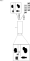
- FIG. 2 is a diagram illustrating a configuration example of a sensor chip and an SoC.
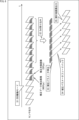
- FIG. 3 is a diagram illustrating the flow of processing related to image correction.
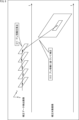
- FIG. 2 is a diagram showing a configuration example of a sensor chip and an SoC according to the first embodiment.
- FIG. 3 is a diagram illustrating the flow of blur correction.
- FIG. 7 is a diagram illustrating a configuration example of a sensor chip and an SoC according to a second embodiment.
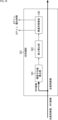
- FIG. 3 is a diagram illustrating a detailed configuration example of an AE processing section.
- FIG. 7 is a diagram illustrating a configuration example of a sensor chip and an SoC according to a third embodiment.
- FIG. 7 is a diagram illustrating a configuration example of a sensor chip and an SoC according to a fourth embodiment.
- FIG. 3 is a diagram illustrating an example of an image output format.
- FIG. 3 is a diagram illustrating processing time and reflection on registers. 1 is a block diagram showing a configuration example of an imaging device.
- FIG. 1 shows a configuration in which a sensor chip outputs image data, a processing circuit (SoC: System-on-a-chip) acquires the image data, and outputs it to a subsequent stage as an image for recording.
- SoC System-on-a-chip
- the processing circuit detects correction data from the acquired image data (frame) and feeds it back to the image for recording, a frame for correction data detection (correction data detection image) is required. Therefore, the frame rate of the corrected image (correction target image) finally output from the processing circuit is reduced. For example, as shown in FIG. 1, when the frame rate of the image data output from the sensor chip is 30 fps and the correction target image is corrected using three consecutive frames as correction data detection images, the frames of the correction target image The rate drops to 7.5fps.
- the sensor chip outputs a narrow-angle image Fn with a reduced angle of view, as shown in the upper part of Figure 2, to improve the frame rate (for high-speed shooting). ) is possible.
- the spatial resolution of the corrected image after the angle of view is corrected becomes low.
- the sensor chip alternately outputs a full-angle image Fs, which is a correction target image, and a plurality of frames of narrow-angle images Fn, which are correction data detection images. It is also possible to maintain spatial resolution. However, in this case, communication related to register control for mode (angle of view) switching occurs between the subsequent SoC and the sensor chip, resulting in increased power consumption.
- correction parameters are calculated based on multiple frames of area images using a sensor that can simultaneously output full-angle images and regional images, and the calculated correction parameters are fed back to the full-angle images. By doing so, it is possible to more appropriately obtain high-quality images.
- An imaging device to which the technology according to the present disclosure is applied employs the imaging element (sensor chip) of Patent Document 1.
- the sensor chip configuring the imaging device 1 to which the technology according to the present disclosure is applied has one AD converter that performs AD (Analog to Digital) conversion on signals read out from pixels. It has a chip structure consisting of a single chip with rows.
- the sensor chip of the present disclosure reads out pixel signals from all regions within a pixel array section (pixel region) at a first frame rate, and reads pixel signals from a specific region (ROI (Region Of Interest)) within the pixel region at a first frame rate. Reading is performed at a second frame rate higher than the first frame rate.
- the second frame rate will also be referred to as a high frame rate.
- the sensor chip of the present disclosure has a structure that performs multiple controls on a single pixel array section and reads out pixel signals in the corresponding area.
- the sensor chip of the present disclosure by devising readout control including AD conversion under multiple controls, the load on circuit resources and power can be suppressed, and the ROI can be achieved by outputting full-angle images and high frame rates. Achieve image output.
- “Outputting an ROI image” refers to outputting a region image of a specific region.
- DSS Dual Speed Stream
- control is performed to read out the pixel signals of the full-angle image at a first frame rate, and the pixel signals of the ROI image are read out at a second frame rate higher than the first frame rate.
- Read control is performed. Among them, for example, the angle of view of the ROI image becomes smaller as its frame rate (second frame rate) becomes higher.
- the vertical ROI component that is, the vertical address information (vertical ROI position information)
- the readout operation of the pixel signal of each pixel in the pixel row in the range including the ROI is repeatedly performed.
- a horizontally long image including the ROI is obtained.
- the horizontal ROI component that is, horizontal address information (horizontal ROI position information)
- only a rectangle in the ROI portion is cut out from this horizontally long image, and other portions are masked. Through such processing, it is possible to reduce the amount of output data.
- the ROI image is an image in which only the ROI portion is cut out from the horizontally long image acquired based on the vertical ROI component, but the horizontally long image acquired based on the vertical ROI component is It may be used as an ROI image as is.
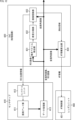
- FIG. 5 is a diagram showing a configuration example of a sensor chip and an SoC to which the technology according to the present disclosure can be applied.
- the sensor chip 10 has a pixel array section 11, a control unit 12, and a data processing section 13, and the SoC 30 has an image recognition section 31 and a processing section 32.
- pixels including photoelectric conversion sections are two-dimensionally arranged in a row direction (horizontal direction) and a column direction (vertical direction), that is, in a matrix.
- the control unit 12 is configured as a pixel control section that performs readout control of pixel signals of pixels in the pixel array section 11 based on various timing signals, clock signals, control signals, and the like.
- the control unit 12 drives each pixel of the pixel array section 11 on a row-by-row basis.
- control unit 12 reads out pixel signals from all pixel areas in the pixel array unit 11 at a first frame rate, and reads out pixel signals from all pixel areas in the pixel array unit 11 based on the ROI position information from the SoC 30. (ROI) pixel signals are read out at a second frame rate (high frame rate).
- ROI ROI
- Such readout control by the control unit 12 makes it possible to simultaneously output one full-angle image of one frame and ROI images of multiple frames.
- the data processing unit 13 is composed of, for example, an AD converter and a latch circuit provided for each pixel column. Specifically, the data processing unit 13 converts analog pixel signals output in pixel row units for each pixel column into digital signals, performs predetermined data processing on the converted pixel data, and then converts the image ( image data) to the SoC 30.
- the data processing unit 13 When the sensor chip 10 is driven in the normal drive mode, the data processing unit 13 outputs a full-angle image at the first frame rate.
- the data processing unit 13 When the sensor chip 10 is driven in the DSS drive mode in which multiple ROI images can be output during one frame period, the data processing unit 13 outputs full-angle images at the first frame rate, and at the same time ROI images are output at a frame rate of
- one full-angle image of one frame and multiple frames of ROI images that are simultaneously output during one frame period are collectively referred to as a frame set.
- the image recognition unit 31 of the SoC 30 determines a specific region (ROI) in the pixel area of the pixel array unit 11 based on image recognition of the full-angle image from the sensor chip 10, and determines the ROI representing the position of the ROI in the pixel area. Position information is output to the sensor chip 10. Thereby, the sensor chip 10 can output an ROI image by reading out the pixel signals of the ROI determined by the SoC 30. Note that the image recognition section 31 can also be provided within the sensor chip 10.
- the processing unit 32 outputs to a subsequent stage a full-angle image in which corrections based on correction parameters calculated based on multiple frames of ROI images from the sensor chip 10 are reflected.
- the processing unit 32 may have the function of a parameter calculation unit that calculates correction parameters.
- the processing unit 32 calculates correction parameters for correcting the full-angle image based on multiple frames of ROI images from the sensor chip 10, and uses the calculated correction parameters to correct the full-angle image. do.
- FIG. 6 it is a diagram explaining the flow of processing related to image correction by the sensor chip 10 and the SoC 30.
- a full-angle image is output from the sensor chip 10 at the first frame rate.
- the sensor chip 10 when driving in the DSS drive mode is set in step S1, the sensor chip 10 outputs full-angle images at the first frame rate, and multiple ROI images are output at the second frame rate. Output at rate.
- the full-angle image is output at 30 fps as a correction target image
- the multiple ROI images are output at 960 fps as correction data detection images.
- the frame rate of the ROI image can be set arbitrarily depending on the field of view of the ROI image, the accuracy of the detected correction data (calculated correction parameters), the purpose of the final output corrected image, etc. ⁇ Can be changed.
- step S2 when the correction target image (full view angle image) and a plurality of correction data detection images (ROI images) are taken into the SoC 30, in step S3, the SoC 30 detects correction data from the plurality of correction data detection images. By doing so, the correction parameters are calculated.
- step S4 the SoC 30 feeds back the calculated correction parameters to the correction target image.
- step S5 the correction target image on which the correction based on the correction parameters is reflected is output as a corrected image.
- one frame of all-angle images and multiple frames of ROI images are output as a frame set every frame period by DSS driving, so correction data can be detected at high speed, and the final It becomes possible to prevent a decrease in the frame rate of the corrected image output from the SoC 30.
- the data processing section 13 of the sensor chip 10 may have the function of a parameter calculation section.
- the data processing unit 13 calculates correction parameters for correcting the full-angle image based on the multiple-frame ROI images without outputting the multiple-frame ROI images to the SoC 30, and calculates the calculated correction parameters. Correct the full-angle image using the parameters.
- FIG. 7 is a diagram illustrating a configuration example of a sensor chip and an SoC according to the first embodiment of the present disclosure.
- the sensor chip 110 includes a pixel array section 111, a control unit 112, and a data processing section 113, and the SoC 130 includes an image recognition section 131, a blur information calculation section 132, and a blur correction section. It has a section 133.
- the pixel array section 111, control unit 112, and data processing section 113 included in the sensor chip 110 are configured similarly to the pixel array section 11, control unit 12, and data processing section 13 described with reference to FIG. Therefore, its explanation will be omitted.
- the image recognition unit 131 included in the SoC 130 is configured similarly to the image recognition unit 31 described with reference to FIG. 5, so the description thereof will be omitted.
- the blur information calculation section 132 and the blur correction section 133 correspond to the processing section 32 described with reference to FIG.
- the blur information calculation unit 132 is configured as a parameter calculation unit in this embodiment.
- the blur information calculation unit 132 calculates blur information representing a blur trajectory (shake amount) by detecting a motion vector as correction data from multiple frames of ROI images from the sensor chip 10, and supplies it to the blur correction unit 133. do.
- the ROI is determined by detecting a subject of interest whose motion vector is to be detected based on image recognition by the image recognition unit 131. That is, the blur information calculation unit 132 calculates blur information by detecting a motion vector from the subject of interest appearing in the ROI image.
- the object of interest to be recognized in image recognition may be specified by the user, for example.
- the blur correction unit 133 corrects blur in the full-angle image from the sensor chip 10 based on the blur information from the blur information calculation unit 132, and outputs the corrected full-angle image to a subsequent stage.
- step S11 the blur information calculation unit 132 calculates blur information by detecting a motion vector between each frame, using the ROI images of multiple frames constituting a certain frame set as correction data detection images.
- step S12 the blur correction unit 133 corrects the blur based on the blur information calculated by the blur information calculation unit 132, using, for example, the full angle of view image forming the next frame set as the correction target image.
- the corrected full-angle image is output to the subsequent stage at, for example, 30 fps.
- FIG. 9 is a diagram illustrating a configuration example of a sensor chip and an SoC according to the second embodiment of the present disclosure.
- the sensor chip 210 has a pixel array section 211, a control unit 212, and a data processing section 213, and the SoC 230 has an image recognition section 231.
- the pixel array section 211 and control unit 212 included in the sensor chip 210 are configured similarly to the pixel array section 11 and the control unit 12, respectively, described with reference to FIG. 5, so a description thereof will be omitted. Further, the image recognition unit 231 included in the SoC 230 is configured similarly to the image recognition unit 31 described with reference to FIG.
- the data processing section 213 of the sensor chip 210 is configured to include a D gain processing section 221 and an AE (automatic exposure) processing section 222.
- the D gain processing unit 221 amplifies each pixel data constituting the image data (full view angle image, ROI image) that is a digital signal based on the D gain (digital gain) calculated by the AE processing unit 222 at the subsequent stage. do.
- the full-angle image and multiple frames of ROI images with amplified pixel data are supplied to the AE processing unit 222.
- the AE processing unit 222 is configured as a parameter calculation unit in this embodiment.
- the AE processing unit 222 acquires brightness data as correction data from the ROI images of multiple frames from the D gain processing unit 221, and calculates AE information (automatic exposure information) based on the acquired brightness data.
- a photometric region from which luminance data is to be acquired is determined as an ROI by scene discrimination based on image recognition by the image recognition unit 231. That is, the AE processing unit 222 obtains brightness data from the photometric area determined by the SoC 230 and calculates AE information.
- the AE processing unit 222 calculates D gain, A (analog) gain, and exposure time as AE information.
- the D gain is supplied to the D gain processing section 221, and the A gain and exposure time are supplied to the control unit 212.
- the control unit 212 drives each pixel of the pixel array section 11 in the DSS drive mode based on the A gain and exposure time from the AE processing section 222.
- the D gain processing unit 221 amplifies the pixel data of the full view angle image and the ROI image based on the D gain from the AE processing unit 222. That is, the sensor chip 210 corrects the brightness of the full-angle image through AE control based on AE information calculated by the AE processing unit 222.
- the AE processing unit 222 outputs the full-angle image from the D gain processing unit 221, that is, the full-angle image whose brightness has been corrected, to the SoC 230 at, for example, 30 fps.
- FIG. 10 is a diagram showing a detailed configuration example of the AE processing section 222.
- the AE processing section 222 shown in FIG. 10 includes a brightness average value calculation section 241, a difference calculation section 242, and a feedback rate multiplication section 243.
- the brightness average value calculation unit 241 acquires brightness data from each of multiple frames of ROI images from the D gain processing unit 221, calculates the average value (brightness average value), and supplies it to the difference calculation unit 242.
- the difference calculation unit 242 calculates a difference value between the brightness average value from the brightness average value calculation unit 241 and a preset target value of brightness data, and supplies it to the feedback rate multiplication unit 243.
- the feedback rate multiplier 243 calculates a feedback rate as a weighting value for the AE information (D gain, A gain, exposure time) based on the difference value from the difference calculation unit 242, and calculates the feedback rate as a weighting value for the AE information (D gain, A gain, exposure time). Multiply each time.
- the weighted D gain is supplied to the D gain processing section 221, and the weighted A gain and exposure time are supplied to the control unit 212.
- FIG. 11 is a diagram illustrating a configuration example of a sensor chip and an SoC according to a third embodiment of the present disclosure.
- the sensor chip 310 includes a pixel array section 311, a control unit 312, and a data processing section 313, and the SoC 330 includes an image recognition section 331 and an AF (autofocus) information calculation section 332. have.
- a lens unit 350 that includes an optical system such as a lens is shown in FIG.
- the lens unit 350 includes an AF control section 351 that performs lens focusing control.
- the pixel array section 311, control unit 312, and data processing section 313 included in the sensor chip 310 are configured in the same manner as the pixel array section 11, control unit 12, and data processing section 13 described with reference to FIG. Therefore, its explanation will be omitted.
- the pixel array section 311 includes phase difference detection pixels that can output phase difference pixel data (phase difference pixel signals) instead of some of the pixels that output normal pixel data (pixel signals).
- the image recognition unit 331 included in the SoC 330 is configured similarly to the image recognition unit 31 described with reference to FIG. 5, so the description thereof will be omitted.
- the AF information calculation section 332 corresponds to the processing section 32 described with reference to FIG.
- the AF information calculation section 332 is configured as a parameter calculation section in this embodiment.
- the AF information calculation unit 332 calculates AF information for performing lens focusing control by acquiring phase difference pixel data as correction data from multiple frames of ROI images from the sensor chip 10, and calculates AF information for performing lens focusing control. is supplied to the AF control section 351 of.
- a cutout region for lens focusing control is determined as an ROI based on image recognition by the image recognition unit 331. That is, the AF information calculation unit 332 acquires phase difference pixel data from the cutout area determined by the SoC 330 and calculates AF information.
- the AF control section 351 of the lens unit 350 performs lens focusing control based on the AF information from the AF information calculation section 332. That is, the AF control section 351 performs phase difference AF control. Thereby, the sensor chip 310 can output a full-angle image whose focus has been corrected (adjusted) to the SoC 330 at, for example, 30 fps.
- AF information can be calculated at high speed, so the focus can be adjusted without reducing the frame rate of the corrected image that is finally output. It becomes possible to obtain appropriately adjusted high-quality images.
- FIG. 12 is a diagram illustrating a configuration example of a sensor chip and an SoC according to a fourth embodiment of the present disclosure.
- the sensor chip 410 includes a pixel array section 411, a control unit 412, and a data processing section 413
- the SoC 430 includes a motion vector detection section 421, a foreground separation section 422, and an image recognition section. 423 and an AF information calculation section 434.
- FIG. 12 shows a lens unit 450 that includes an optical system such as a lens in addition to the sensor chip 410 and the SoC 430.
- the lens unit 450 includes an AF control section 451 that performs lens focusing control.
- the pixel array section 411, control unit 412, and data processing section 413 included in the sensor chip 410 are configured similarly to the pixel array section 11, control unit 12, and data processing section 13 described with reference to FIG. 5, respectively. Therefore, its explanation will be omitted.
- the image recognition unit 433 included in the SoC 430 is basically configured in the same way as the image recognition unit 31 described with reference to FIG.
- the motion vector detection section 431, the foreground separation section 432, and the AF information calculation section 434 correspond to the processing section 32 described with reference to FIG.
- the motion vector detection unit 431 detects a motion vector as correction data from multiple frames of ROI images from the sensor chip 410. Specifically, the motion vector detection unit 431 detects a motion vector for each pixel between frames of multiple frames of ROI images forming a frame set.
- the foreground separation unit 432 is configured as a parameter calculation unit in this embodiment.
- the foreground separation unit 432 specifies the foreground area by separating the foreground area and the background area in the ROI image based on the motion vector for each pixel detected by the motion vector detection unit 431.
- the image recognition unit 433 is a photometry area that measures a contrast value used for lens focusing control based on the foreground area specified by the foreground separation unit 432 and the subject area detected by image recognition for the full-angle image. is determined as the ROI.
- ROI position information representing the position of the ROI is output to the sensor chip 410, and information representing the photometric area is supplied to the AF information calculation unit 434.
- the AF information calculation unit 434 measures the contrast value of the photometric area represented by the information from the image recognition unit 433 in the full-angle image from the sensor chip 410, thereby calculating the AF information for controlling the focus of the lens.
- the information is calculated and supplied to the AF control section 451 of the lens unit 450.
- the AF control section 451 of the lens unit 450 performs lens focusing control based on the AF information from the AF information calculation section 434. That is, the AF control unit 451 performs contrast AF control. Thereby, the sensor chip 410 can output to the SoC 430 a full-angle image with the focus adjusted on the desired subject area at, for example, 30 fps.
- Capacity of ROM (RAM) for storing high frame rate ROI images In an SoC like the first embodiment described above, depending on the number of ROI image frames required to calculate blur information, It is necessary to secure the capacity of ROM (Read Only Memory) and RAM (Random Access Memory).
- the processing time required for correction based on the correction parameters calculated from the correction data detection image output at a high frame rate is The correction must be completed before the register reflection of the correction target image (post-correction image) of the frame set. If the processing time is not in time for the register reflection of the correction target image (corrected image) of the next frame set, the correction based on the correction parameter will be reflected in the correction target images of the frameset one after another. It turns out.
- the technology according to the present disclosure can be applied to various products. More specifically, it can be applied to electronic devices such as imaging devices such as digital still cameras and video cameras, mobile terminal devices with an imaging function such as mobile phones, and copying machines that use an imaging element in the image reading section. .
- electronic devices such as imaging devices such as digital still cameras and video cameras
- mobile terminal devices with an imaging function such as mobile phones
- copying machines that use an imaging element in the image reading section.
- a case where the present invention is applied to an imaging device such as a digital still camera or a video camera will be described below.
- FIG. 15 is a block diagram showing the configuration of an imaging device that is an example of an electronic device.
- an imaging apparatus 500 includes an imaging optical system 501 including a lens group, an imaging unit 502, a DSP (Digital Signal Processor) circuit 503, a frame memory 504, a display device 505, a recording It is configured to include a device 506, an operation system 507, and a power supply system 508.
- the DSP circuit 503, frame memory 504, display device 505, recording device 506, operation system 507, and power supply system 508 are interconnected via a bus line 509.
- the imaging optical system 501 takes in incident light (image light) from a subject and forms an image on the imaging surface of the imaging unit 502.
- the imaging unit 502 converts the amount of incident light imaged onto the imaging surface by the imaging optical system 501 into an electrical signal for each pixel, and outputs the electric signal as a pixel signal.
- the DSP circuit 503 performs general camera signal processing, such as white balance processing, demosaic processing, and gamma correction processing.
- the frame memory 504 is used to store data as appropriate during the signal processing process in the DSP circuit 503.
- the display device 505 is composed of a panel type display device such as a liquid crystal display device or an organic EL (Electro Luminescence) display device, and displays a moving image or a still image captured by the imaging unit 502.
- a recording device 506 records a moving image or a still image captured by the imaging unit 502 on a recording medium such as a portable semiconductor memory, an optical disk, or an HDD (Hard Disk Drive).
- the operation system 507 issues operation commands for various functions of the imaging device 500 under operation by the user.
- a power supply system 508 appropriately supplies various kinds of power that serve as operating power for the DSP circuit 503, frame memory 504, display device 505, recording device 506, and operation system 507 to these supply targets.
- the imaging device 500 having the above configuration, the sensor chip capable of DSS driving of the embodiment described above and the SoC that feeds back ROI position information to the sensor chip in real time can be used as the imaging unit 502 and the DSP 503, respectively. . Therefore, the imaging device 500 can also more appropriately acquire high-quality images.
- the present disclosure can take the following configuration. (1) By reading out the pixel signals of all the pixel areas at a first frame rate and reading out the pixel signals of a specific area in the pixel area at a second frame rate higher than the first frame rate, the entire viewing angle of one frame can be read out.
- a sensor chip having a pixel control unit capable of simultaneously outputting an image and regional images of multiple frames; a parameter calculation unit that calculates a correction parameter for correction of the full view angle image based on the area images of a plurality of frames; an imaging device comprising: a processing circuit that outputs to a subsequent stage the full angle of view image on which the correction based on the correction parameter is reflected; (2) The imaging device according to (1), wherein the processing circuit outputs the full-angle image corrected using the correction parameter to a subsequent stage. (3) The imaging device according to (1), wherein the sensor chip outputs the full-angle image corrected using the correction parameter to the processing circuit.
- the processing circuit determines the specific area in the pixel area based on image recognition for the full view angle image, The imaging device according to (1), wherein the sensor chip outputs the area image by reading out pixel signals of the specific area determined by the processing circuit.
- the parameter calculation unit calculates blur information based on motion vectors detected from the area images of multiple frames, The imaging device according to (2) or (4), wherein the processing circuit corrects blur in the full-angle image based on the calculated blur information.
- the parameter calculation unit calculates automatic exposure information based on brightness data acquired from the area images of multiple frames, The imaging device according to (3) or (4), wherein the sensor chip corrects the brightness of the full-angle image by automatic exposure control based on the calculated automatic exposure information.
- the sensor chip includes a phase difference detection pixel capable of outputting phase difference pixel data in the pixel region, The imaging device according to (4), wherein the parameter calculation unit calculates focus control information for controlling lens focus based on the phase difference pixel data acquired from the area images of a plurality of frames.
- the imaging device further comprising a focus control section that performs focus control of the lens based on the calculated focus control information.
- the processing circuit determines a cutout area for controlling the focus of the lens as the specific area based on the image recognition.
- the parameter calculation unit identifies a foreground region based on motion vectors detected from the region images of multiple frames;
- the processing circuit determines, as the specific area, a photometric area for measuring a contrast value used for lens focusing control, based on the specified foreground area and the subject area detected by the image recognition.
- the imaging device according to 4).
- the imaging device (13) The imaging device according to (12), wherein the processing circuit calculates focus control information for controlling focus of the lens based on the contrast value measured in the photometry area. (14) The imaging device according to (13), further comprising a focus control section that performs focus control of the lens based on the calculated focus control information. (15) By reading out the pixel signals of all the pixel areas at a first frame rate and reading out the pixel signals of a specific area in the pixel area at a second frame rate higher than the first frame rate, the entire viewing angle of one frame can be read out.
- a pixel control unit that can simultaneously output an image and a region image of multiple frames; a parameter calculation unit that calculates a correction parameter for correction of the full view angle image based on the area images of a plurality of frames; and a processing unit that outputs the full-angle image corrected using the correction parameter.
- a parameter calculation unit that calculates a correction parameter for correcting the full-angle image based on the plurality of frames of area images output from a sensor chip that is capable of simultaneously outputting an image and a plurality of frames of area images; and a processing unit that outputs the full angle of view image corrected using the correction parameter to a subsequent stage.
Landscapes
- Engineering & Computer Science (AREA)
- Multimedia (AREA)
- Signal Processing (AREA)
- Physics & Mathematics (AREA)
- General Physics & Mathematics (AREA)
- Theoretical Computer Science (AREA)
- Computer Vision & Pattern Recognition (AREA)
- Studio Devices (AREA)
Abstract
Description
2.DSS駆動について
3.センサチップとSoCの構成および動作
4.第1の実施形態(ブレ補正の例)
5.第2の実施形態(明るさ補正の例)
6.第3の実施形態(位相差AFによる合焦制御の例)
7.第4の実施形態(コントラストAFの性能向上の例)
8.SoCに求められるスペック
9.適用例
図1には、センサチップが画像データを出力し、処理回路(SoC:System-on-a-chip)が画像データを取得し、記録用の画像として後段に出力する構成が示されている。
特許文献1に開示されているように、画素アレイ部内の全画素の信号を第1のフレームレートで読み出すとともに、画素アレイ部内の特定の領域の画素の信号を第1のフレームレートよりも高い第2のフレームレートで読み出す撮像素子が知られている。
ここで、上述したDSS駆動が可能なセンサチップと、画素領域におけるROIの位置を表すROI位置情報をセンサチップにリアルタイムにフィードバックするSoC(処理回路)の構成とその動作について説明する。
図7は、本開示の第1の実施形態のセンサチップとSoCの構成例を示す図である。
図9は、本開示の第2の実施形態のセンサチップとSoCの構成例を示す図である。
図11は、本開示の第3の実施形態のセンサチップとSoCの構成例を示す図である。
図12は、本開示の第4の実施形態のセンサチップとSoCの構成例を示す図である。
DSS駆動モードで駆動するセンサチップから高フレームレートで出力されるROI画像を処理するSoC(処理回路)側には、一定のスペックが求められる。
上述した第1の実施形態のようなSoCにおいては、ブレ情報を算出するために必要なROI画像のフレーム数に応じて、ROM(Read Only Memory)やRAM(Random Access Memory)の容量を確保する必要がある。
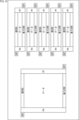
DSS駆動モードで駆動するセンサチップからは、図13の左側に示される、通常の出力フォーマットの画像(全画角画像)に加え、例えば、同図右側に示される、ROIに対応する特殊な出力フォーマットの画像(ROI画像)が複数出力される。SoC側では、このような特殊な出力フォーマットの画像データを受け入れる性能が必要とされる。なお、センサチップから画像データとして出力される全画角画像と複数のROI画像とは、互いに非同期で(異なるタイミングで)出力される。
図14に示されるように、高フレームレートで出力される補正データ検出画像から算出した補正パラメータに基づいた補正に要する処理時間は、補正が反映される次のフレームセットの補正対象画像(補正後画像)のレジスタ反映のタイミングより前に完了している必要がある。仮に、処理時間が、次のフレームセットの補正対象画像(補正後画像)のレジスタ反映のタイミングに間に合わないような場合、補正パラメータに基づいた補正は、次々フレームセットの補正対象画像に反映されることになる。
本開示に係る技術は、様々な製品に適用することができる。より具体的には、デジタルスチルカメラやビデオカメラなどの撮像装置や、携帯電話機などの撮像機能を有する携帯端末装置、画像読取部に撮像素子を用いる複写機などの電子機器に適用することができる。以下、デジタルスチルカメラやビデオカメラなどの撮像装置に適用する場合について説明する。
さらに、本開示は以下のような構成をとることができる。
(1)
画素領域全ての画素信号を第1のフレームレートで読み出すとともに、前記画素領域における特定領域の画素信号を前記第1のフレームレートより高い第2のフレームレートで読み出すことで、1フレームの全画角画像と複数フレームの領域画像を同時に出力可能とする画素制御部を有するセンサチップと、
複数フレームの前記領域画像に基づいて、前記全画角画像の補正のための補正パラメータを算出するパラメータ算出部と、
前記補正パラメータに基づいた補正が反映された前記全画角画像を後段に出力する処理部を有する処理回路と
を備える撮像装置。
(2)
前記処理回路は、前記補正パラメータを用いて補正した前記全画角画像を後段に出力する
(1)に記載の撮像装置。
(3)
前記センサチップは、前記補正パラメータを用いて補正した前記全画角画像を前記処理回路に出力する
(1)に記載の撮像装置。
(4)
前記処理回路は、前記全画角画像に対する画像認識に基づいて前記画素領域における前記特定領域を決定し、
前記センサチップは、前記処理回路により決定された前記特定領域の画素信号を読み出すことで前記領域画像を出力する
(1)に記載の撮像装置。
(5)
前記パラメータ算出部は、複数フレームの前記領域画像から検出された動きベクトルに基づいてブレ情報を算出し、
前記処理回路は、算出された前記ブレ情報に基づいて、前記全画角画像のブレを補正する
(2)または(4)に記載の撮像装置。
(6)
前記処理回路は、前記画像認識に基づいて、前記動きベクトルの検出対象となる注目被写体を検出することで、前記特定領域を決定する
(5)に記載の撮像装置。
(7)
前記パラメータ算出部は、複数フレームの前記領域画像から取得された輝度データに基づいて自動露出情報を算出し、
前記センサチップは、算出された前記自動露出情報に基づいた自動露出制御により、前記全画角画像の明るさを補正する
(3)または(4)に記載の撮像装置。
(8)
前記処理回路は、前記画像認識に基づいたシーン判別により、前記輝度データの取得対象となる測光領域を、前記特定領域として決定する
(7)に記載の撮像装置。
(9)
前記センサチップは、前記画素領域に位相差画素データを出力可能な位相差検出画素を含み、
前記パラメータ算出部は、複数フレームの前記領域画像から取得された前記位相差画素データに基づいて、レンズの合焦制御を行うための合焦制御情報を算出する
(4)に記載の撮像装置。
(10)
算出された前記合焦制御情報に基づいて、前記レンズの合焦制御を行う合焦制御部をさらに備える
(9)に記載の撮像装置。
(11)
前記処理回路は、前記画像認識に基づいて、前記レンズの合焦制御のための切り出し領域を、前記特定領域として決定する
(9)または(10)に記載の撮像装置。
(12)
前記パラメータ算出部は、複数フレームの前記領域画像から検出された動きベクトルに基づいて前景領域を特定し、
前記処理回路は、特定された前記前景領域と、前記画像認識により検出された被写体領域に基づいて、レンズの合焦制御に用いられるコントラスト値を計測する測光領域を、前記特定領域として決定する
(4)に記載の撮像装置。
(13)
前記処理回路は、前記測光領域において計測された前記コントラスト値に基づいて、前記レンズの合焦制御を行うための合焦制御情報を算出する
(12)に記載の撮像装置。
(14)
算出された前記合焦制御情報に基づいて、前記レンズの合焦制御を行う合焦制御部をさらに備える
(13)に記載の撮像装置。
(15)
画素領域全ての画素信号を第1のフレームレートで読み出すとともに、前記画素領域における特定領域の画素信号を前記第1のフレームレートより高い第2のフレームレートで読み出すことで、1フレームの全画角画像と複数フレームの領域画像を同時に出力可能とする画素制御部と、
複数フレームの前記領域画像に基づいて、前記全画角画像の補正のための補正パラメータを算出するパラメータ算出部と、
前記補正パラメータを用いて補正した前記全画角画像を出力する処理部と
を備えるセンサチップ。
(16)
画素領域全ての画素信号を第1のフレームレートで読み出すとともに、前記画素領域における特定領域の画素信号を前記第1のフレームレートより高い第2のフレームレートで読み出すことで、1フレームの全画角画像と複数フレームの領域画像を同時に出力可能とするセンサチップから出力された複数フレームの前記領域画像に基づいて、前記全画角画像の補正のための補正パラメータを算出するパラメータ算出部と、
前記補正パラメータを用いて補正した前記全画角画像を後段に出力する処理部と
を備える処理回路。
Claims (16)
- 画素領域全ての画素信号を第1のフレームレートで読み出すとともに、前記画素領域における特定領域の画素信号を前記第1のフレームレートより高い第2のフレームレートで読み出すことで、1フレームの全画角画像と複数フレームの領域画像を同時に出力可能とする画素制御部を有するセンサチップと、
複数フレームの前記領域画像に基づいて、前記全画角画像の補正のための補正パラメータを算出するパラメータ算出部と、
前記補正パラメータに基づいた補正が反映された前記全画角画像を後段に出力する処理部を有する処理回路と
を備える撮像装置。 - 前記処理回路は、前記補正パラメータを用いて補正した前記全画角画像を後段に出力する
請求項1に記載の撮像装置。 - 前記センサチップは、前記補正パラメータを用いて補正した前記全画角画像を前記処理回路に出力する
請求項1に記載の撮像装置。 - 前記処理回路は、前記全画角画像に対する画像認識に基づいて前記画素領域における前記特定領域を決定し、
前記センサチップは、前記処理回路により決定された前記特定領域の画素信号を読み出すことで前記領域画像を出力する
請求項1に記載の撮像装置。 - 前記パラメータ算出部は、複数フレームの前記領域画像から検出された動きベクトルに基づいてブレ情報を算出し、
前記処理回路は、算出された前記ブレ情報に基づいて、前記全画角画像のブレを補正する
請求項4に記載の撮像装置。 - 前記処理回路は、前記画像認識に基づいて、前記動きベクトルの検出対象となる注目被写体を検出することで、前記特定領域を決定する
請求項5に記載の撮像装置。 - 前記パラメータ算出部は、複数フレームの前記領域画像から取得された輝度データに基づいて自動露出情報を算出し、
前記センサチップは、算出された前記自動露出情報に基づいた自動露出制御により、前記全画角画像の明るさを補正する
請求項4に記載の撮像装置。 - 前記処理回路は、前記画像認識に基づいたシーン判別により、前記輝度データの取得対象となる測光領域を、前記特定領域として決定する
請求項7に記載の撮像装置。 - 前記センサチップは、前記画素領域に位相差画素データを出力可能な位相差検出画素を含み、
前記パラメータ算出部は、複数フレームの前記領域画像から取得された前記位相差画素データに基づいて、レンズの合焦制御を行うための合焦制御情報を算出する
請求項4に記載の撮像装置。 - 算出された前記合焦制御情報に基づいて、前記レンズの合焦制御を行う合焦制御部をさらに備える
請求項9に記載の撮像装置。 - 前記処理回路は、前記画像認識に基づいて、前記レンズの合焦制御のための切り出し領域を、前記特定領域として決定する
請求項9に記載の撮像装置。 - 前記パラメータ算出部は、複数フレームの前記領域画像から検出された動きベクトルに基づいて前景領域を特定し、
前記処理回路は、特定された前記前景領域と、前記画像認識により検出された被写体領域に基づいて、レンズの合焦制御に用いられるコントラスト値を計測する測光領域を、前記特定領域として決定する
請求項4に記載の撮像装置。 - 前記処理回路は、前記測光領域において計測された前記コントラスト値に基づいて、前記レンズの合焦制御を行うための合焦制御情報を算出する
請求項12に記載の撮像装置。 - 算出された前記合焦制御情報に基づいて、前記レンズの合焦制御を行う合焦制御部をさらに備える
請求項13に記載の撮像装置。 - 画素領域全ての画素信号を第1のフレームレートで読み出すとともに、前記画素領域における特定領域の画素信号を前記第1のフレームレートより高い第2のフレームレートで読み出すことで、1フレームの全画角画像と複数フレームの領域画像を同時に出力可能とする画素制御部と、
複数フレームの前記領域画像に基づいて、前記全画角画像の補正のための補正パラメータを算出するパラメータ算出部と、
前記補正パラメータを用いて補正した前記全画角画像を出力する処理部と
を備えるセンサチップ。 - 画素領域全ての画素信号を第1のフレームレートで読み出すとともに、前記画素領域における特定領域の画素信号を前記第1のフレームレートより高い第2のフレームレートで読み出すことで、1フレームの全画角画像と複数フレームの領域画像を同時に出力可能とするセンサチップから出力された複数フレームの前記領域画像に基づいて、前記全画角画像の補正のための補正パラメータを算出するパラメータ算出部と、
前記補正パラメータを用いて補正した前記全画角画像を後段に出力する処理部と
を備える処理回路。
Priority Applications (1)
| Application Number | Priority Date | Filing Date | Title |
|---|---|---|---|
| US18/863,037 US12598389B2 (en) | 2022-05-13 | 2023-04-27 | Imaging device, sensor chip, and processing circuit |
Applications Claiming Priority (2)
| Application Number | Priority Date | Filing Date | Title |
|---|---|---|---|
| JP2022079195 | 2022-05-13 | ||
| JP2022-079195 | 2022-05-13 |
Publications (1)
| Publication Number | Publication Date |
|---|---|
| WO2023218980A1 true WO2023218980A1 (ja) | 2023-11-16 |
Family
ID=88730430
Family Applications (1)
| Application Number | Title | Priority Date | Filing Date |
|---|---|---|---|
| PCT/JP2023/016577 Ceased WO2023218980A1 (ja) | 2022-05-13 | 2023-04-27 | 撮像装置、センサチップ、および処理回路 |
Country Status (2)
| Country | Link |
|---|---|
| US (1) | US12598389B2 (ja) |
| WO (1) | WO2023218980A1 (ja) |
Citations (5)
| Publication number | Priority date | Publication date | Assignee | Title |
|---|---|---|---|---|
| JP2000078483A (ja) * | 1998-09-03 | 2000-03-14 | Canon Inc | 固体撮像装置と自動露光装置 |
| JP2008252648A (ja) * | 2007-03-30 | 2008-10-16 | Casio Comput Co Ltd | 撮像装置及びプログラム |
| JP2015119206A (ja) * | 2013-12-16 | 2015-06-25 | キヤノン株式会社 | 画像処理装置、その制御方法及びプログラム |
| WO2020218201A1 (ja) * | 2019-04-26 | 2020-10-29 | 富士フイルム株式会社 | 撮像素子、撮像装置、撮像素子の作動方法、及びプログラム |
| WO2021033388A1 (ja) * | 2019-08-20 | 2021-02-25 | ソニーセミコンダクタソリューションズ株式会社 | 撮像素子、撮像素子の駆動方法、及び、電子機器 |
Family Cites Families (3)
| Publication number | Priority date | Publication date | Assignee | Title |
|---|---|---|---|---|
| JP3937924B2 (ja) * | 2002-05-23 | 2007-06-27 | キヤノン株式会社 | 撮像装置及びその制御方法 |
| US9256116B2 (en) * | 2010-03-29 | 2016-02-09 | Fujifilm Corporation | Stereoscopic imaging device, image reproducing device, and editing software |
| JP6486288B2 (ja) * | 2016-02-09 | 2019-03-20 | キヤノン株式会社 | 撮像装置、制御方法、プログラム、記憶媒体 |
-
2023
- 2023-04-27 WO PCT/JP2023/016577 patent/WO2023218980A1/ja not_active Ceased
- 2023-04-27 US US18/863,037 patent/US12598389B2/en active Active
Patent Citations (5)
| Publication number | Priority date | Publication date | Assignee | Title |
|---|---|---|---|---|
| JP2000078483A (ja) * | 1998-09-03 | 2000-03-14 | Canon Inc | 固体撮像装置と自動露光装置 |
| JP2008252648A (ja) * | 2007-03-30 | 2008-10-16 | Casio Comput Co Ltd | 撮像装置及びプログラム |
| JP2015119206A (ja) * | 2013-12-16 | 2015-06-25 | キヤノン株式会社 | 画像処理装置、その制御方法及びプログラム |
| WO2020218201A1 (ja) * | 2019-04-26 | 2020-10-29 | 富士フイルム株式会社 | 撮像素子、撮像装置、撮像素子の作動方法、及びプログラム |
| WO2021033388A1 (ja) * | 2019-08-20 | 2021-02-25 | ソニーセミコンダクタソリューションズ株式会社 | 撮像素子、撮像素子の駆動方法、及び、電子機器 |
Also Published As
| Publication number | Publication date |
|---|---|
| US12598389B2 (en) | 2026-04-07 |
| US20250301224A1 (en) | 2025-09-25 |
Similar Documents
| Publication | Publication Date | Title |
|---|---|---|
| US7839444B2 (en) | Solid-state image-pickup device, method of driving solid-state image-pickup device and image-pickup apparatus | |
| JP6019692B2 (ja) | 撮像素子、撮像素子の制御方法、および、撮像装置 | |
| JP4887275B2 (ja) | 撮像装置及びそのシャッタ駆動モード選択方法 | |
| CN101662589B (zh) | 摄像设备及其控制方法 | |
| US9531944B2 (en) | Focus detection apparatus and control method thereof | |
| US9843735B2 (en) | Image processing apparatus, imaging apparatus comprising the same, and image processing method | |
| EP2212731B1 (en) | Image sensing apparatus | |
| JP2017216646A (ja) | 撮像素子、撮像装置、および撮像信号処理方法 | |
| EP2355491A1 (en) | Imaging device, imaging method and imaging program | |
| CN102857700B (zh) | 摄像设备及其控制方法 | |
| JP2020053771A (ja) | 画像処理装置、撮像装置 | |
| JP5199736B2 (ja) | 画像撮像装置 | |
| CN104641276A (zh) | 摄像装置及信号处理方法 | |
| US8125541B2 (en) | Image-sensing apparatus | |
| US6867803B1 (en) | Image processing unit | |
| US20200358949A1 (en) | Image capturing apparatus and control method therefor | |
| JP5387341B2 (ja) | 撮像装置 | |
| US11206344B2 (en) | Image pickup apparatus and storage medium | |
| JP2006148550A (ja) | 画像処理装置及び撮像装置 | |
| US9282245B2 (en) | Image capturing apparatus and method of controlling the same | |
| JP4739998B2 (ja) | 撮像装置 | |
| WO2023218980A1 (ja) | 撮像装置、センサチップ、および処理回路 | |
| US11202015B2 (en) | Control apparatus and control method | |
| JPWO2018021034A1 (ja) | 撮像制御装置および撮像制御方法、並びに撮像素子 | |
| US20170085779A1 (en) | Imaging control apparatus, imaging apparatus, and imaging control method |
Legal Events
| Date | Code | Title | Description |
|---|---|---|---|
| 121 | Ep: the epo has been informed by wipo that ep was designated in this application |
Ref document number: 23803459 Country of ref document: EP Kind code of ref document: A1 |
|
| WWE | Wipo information: entry into national phase |
Ref document number: 18863037 Country of ref document: US |
|
| NENP | Non-entry into the national phase |
Ref country code: DE |
|
| 122 | Ep: pct application non-entry in european phase |
Ref document number: 23803459 Country of ref document: EP Kind code of ref document: A1 |
|
| NENP | Non-entry into the national phase |
Ref country code: JP |
|
| WWP | Wipo information: published in national office |
Ref document number: 18863037 Country of ref document: US |
|
| WWG | Wipo information: grant in national office |
Ref document number: 18863037 Country of ref document: US |