WO2023218628A1 - 表示装置、発光装置及び照明装置 - Google Patents
表示装置、発光装置及び照明装置 Download PDFInfo
- Publication number
- WO2023218628A1 WO2023218628A1 PCT/JP2022/020168 JP2022020168W WO2023218628A1 WO 2023218628 A1 WO2023218628 A1 WO 2023218628A1 JP 2022020168 W JP2022020168 W JP 2022020168W WO 2023218628 A1 WO2023218628 A1 WO 2023218628A1
- Authority
- WO
- WIPO (PCT)
- Prior art keywords
- layer
- light emitting
- region
- emitting element
- display device
- Prior art date
- Legal status (The legal status is an assumption and is not a legal conclusion. Google has not performed a legal analysis and makes no representation as to the accuracy of the status listed.)
- Ceased
Links
Images







Classifications
-
- H—ELECTRICITY
- H10—SEMICONDUCTOR DEVICES; ELECTRIC SOLID-STATE DEVICES NOT OTHERWISE PROVIDED FOR
- H10K—ORGANIC ELECTRIC SOLID-STATE DEVICES
- H10K50/00—Organic light-emitting devices
- H10K50/10—OLEDs or polymer light-emitting diodes [PLED]
- H10K50/11—OLEDs or polymer light-emitting diodes [PLED] characterised by the electroluminescent [EL] layers
- H10K50/115—OLEDs or polymer light-emitting diodes [PLED] characterised by the electroluminescent [EL] layers comprising active inorganic nanostructures, e.g. luminescent quantum dots
-
- G—PHYSICS
- G02—OPTICS
- G02B—OPTICAL ELEMENTS, SYSTEMS OR APPARATUS
- G02B5/00—Optical elements other than lenses
- G02B5/20—Filters
-
- H—ELECTRICITY
- H05—ELECTRIC TECHNIQUES NOT OTHERWISE PROVIDED FOR
- H05B—ELECTRIC HEATING; ELECTRIC LIGHT SOURCES NOT OTHERWISE PROVIDED FOR; CIRCUIT ARRANGEMENTS FOR ELECTRIC LIGHT SOURCES, IN GENERAL
- H05B33/00—Electroluminescent light sources
- H05B33/12—Light sources with substantially two-dimensional [2D] radiating surfaces
-
- H—ELECTRICITY
- H05—ELECTRIC TECHNIQUES NOT OTHERWISE PROVIDED FOR
- H05B—ELECTRIC HEATING; ELECTRIC LIGHT SOURCES NOT OTHERWISE PROVIDED FOR; CIRCUIT ARRANGEMENTS FOR ELECTRIC LIGHT SOURCES, IN GENERAL
- H05B33/00—Electroluminescent light sources
- H05B33/12—Light sources with substantially two-dimensional [2D] radiating surfaces
- H05B33/14—Light sources with substantially two-dimensional [2D] radiating surfaces characterised by the chemical or physical composition or the arrangement of the electroluminescent material, or by the simultaneous addition of the electroluminescent material in or onto the light source
-
- H—ELECTRICITY
- H10—SEMICONDUCTOR DEVICES; ELECTRIC SOLID-STATE DEVICES NOT OTHERWISE PROVIDED FOR
- H10K—ORGANIC ELECTRIC SOLID-STATE DEVICES
- H10K50/00—Organic light-emitting devices
-
- H—ELECTRICITY
- H10—SEMICONDUCTOR DEVICES; ELECTRIC SOLID-STATE DEVICES NOT OTHERWISE PROVIDED FOR
- H10K—ORGANIC ELECTRIC SOLID-STATE DEVICES
- H10K50/00—Organic light-emitting devices
- H10K50/10—OLEDs or polymer light-emitting diodes [PLED]
- H10K50/19—Tandem OLEDs
-
- H—ELECTRICITY
- H10—SEMICONDUCTOR DEVICES; ELECTRIC SOLID-STATE DEVICES NOT OTHERWISE PROVIDED FOR
- H10K—ORGANIC ELECTRIC SOLID-STATE DEVICES
- H10K59/00—Integrated devices, or assemblies of multiple devices, comprising at least one organic light-emitting element covered by group H10K50/00
-
- H—ELECTRICITY
- H10—SEMICONDUCTOR DEVICES; ELECTRIC SOLID-STATE DEVICES NOT OTHERWISE PROVIDED FOR
- H10K—ORGANIC ELECTRIC SOLID-STATE DEVICES
- H10K59/00—Integrated devices, or assemblies of multiple devices, comprising at least one organic light-emitting element covered by group H10K50/00
- H10K59/30—Devices specially adapted for multicolour light emission
- H10K59/35—Devices specially adapted for multicolour light emission comprising red-green-blue [RGB] subpixels
-
- H—ELECTRICITY
- H10—SEMICONDUCTOR DEVICES; ELECTRIC SOLID-STATE DEVICES NOT OTHERWISE PROVIDED FOR
- H10K—ORGANIC ELECTRIC SOLID-STATE DEVICES
- H10K59/00—Integrated devices, or assemblies of multiple devices, comprising at least one organic light-emitting element covered by group H10K50/00
- H10K59/30—Devices specially adapted for multicolour light emission
- H10K59/35—Devices specially adapted for multicolour light emission comprising red-green-blue [RGB] subpixels
- H10K59/353—Devices specially adapted for multicolour light emission comprising red-green-blue [RGB] subpixels characterised by the geometrical arrangement of the RGB subpixels
-
- H—ELECTRICITY
- H10—SEMICONDUCTOR DEVICES; ELECTRIC SOLID-STATE DEVICES NOT OTHERWISE PROVIDED FOR
- H10K—ORGANIC ELECTRIC SOLID-STATE DEVICES
- H10K59/00—Integrated devices, or assemblies of multiple devices, comprising at least one organic light-emitting element covered by group H10K50/00
- H10K59/30—Devices specially adapted for multicolour light emission
- H10K59/38—Devices specially adapted for multicolour light emission comprising colour filters or colour changing media [CCM]
-
- H—ELECTRICITY
- H10—SEMICONDUCTOR DEVICES; ELECTRIC SOLID-STATE DEVICES NOT OTHERWISE PROVIDED FOR
- H10K—ORGANIC ELECTRIC SOLID-STATE DEVICES
- H10K2102/00—Constructional details relating to the organic devices covered by this subclass
- H10K2102/301—Details of OLEDs
- H10K2102/331—Nanoparticles used in non-emissive layers, e.g. in packaging layer
-
- H—ELECTRICITY
- H10—SEMICONDUCTOR DEVICES; ELECTRIC SOLID-STATE DEVICES NOT OTHERWISE PROVIDED FOR
- H10K—ORGANIC ELECTRIC SOLID-STATE DEVICES
- H10K2102/00—Constructional details relating to the organic devices covered by this subclass
- H10K2102/301—Details of OLEDs
- H10K2102/351—Thickness
Definitions
- the present disclosure relates to a display device, a light emitting device, and a lighting device.
- light-emitting devices that include a wavelength conversion layer that includes a light-emitting layer that includes quantum dots
- lighting devices that include a light-emitting region that includes a light-emitting layer that includes quantum dots. Development is actively underway.
- nanoparticles such as quantum dots are used as part of a functional layer, including a light-emitting layer
- their use in combination with halogen ligands is significantly lower than when used in combination with non-halogen ligands. It is known that luminous efficiency can be improved.
- Non-Patent Document 1 carrier balance and luminous efficiency are improved by forming the amount of halogen ligand contained in a quantum dot layer included in a QLED so as to have a gradient in the stacking direction of the quantum dot layer. It is stated that it can be done.
- the inventors of the present disclosure have discovered that a layer containing nanoparticles such as quantum dots and a relatively high concentration of halogen ligand easily breaks at locations where mechanical stress is generated.
- Non-Patent Document 1 is formed so that the amount of halogen ligand has a gradient in the stacking direction of the quantum dot layers, but since it contains a relatively high concentration of halogen ligand, such a QLED
- QLEDs are provided over the entire display area of a display device, there is a problem that damage to the QLED occurs in areas near the edges of the display area, which are areas where mechanical stress is likely to occur.
- One aspect of the present disclosure has been made in view of the above problems, and provides a display device, a light emitting device, and a lighting device that can suppress damage at locations where mechanical stress occurs and achieve luminous efficiency.
- the purpose is to provide the following.
- the display device of the present disclosure has the following features: a display area including a first area including at least a part of the center of the display area and a second area including at least a part of the edge of the display area; a first light emitting element provided in the first region; a second light emitting element provided in the second region,
- the first light emitting element and the second light emitting element each include: a first electrode and a second electrode; a nanoparticle layer containing nanoparticles located between the first electrode and the second electrode, The concentration of halogen atoms contained in the first layer, which is the nanoparticle layer, of the first light emitting element is higher than the concentration of halogen atoms contained in the second layer, which is the nanoparticle layer, of the second light emitting element.
- the display device of the present disclosure has the following features: a display area including a first area including at least a part of the center of the display area and a second area including at least a part of the edge of the display area; a first light emitting element provided in the first region; a second light emitting element provided in the second region,
- the first light emitting element and the second light emitting element each include: a first electrode and a second electrode; a nanoparticle layer containing nanoparticles located between the first electrode and the second electrode,
- the center position of the maximum thickness of each of the first layer, which is the nanoparticle layer of the first light emitting element, and the second layer, which is the nanoparticle layer of the second light emitting element, is the reference position, and
- the number of parts of the third layer formed directly above the first layer entering the first layer below the reference position is defined as a first number
- the fourth layer formed immediately above the second layer is the number
- the number of parts that have entered the second layer below the position is a second number, The first
- the display device of the present disclosure has the following features: a display area including a first area including at least a part of the center of the display area and a second area including at least a part of the edge of the display area; a first light emitting element provided in the first region; a second light emitting element provided in the second region,
- the first light emitting element and the second light emitting element each include: a first electrode and a second electrode; a nanoparticle layer containing nanoparticles located between the first electrode and the second electrode, a third layer formed immediately above the first layer that is the nanoparticle layer of the first light emitting element; and a fourth layer formed immediately above the second layer that is the nanoparticle layer of the second light emitting element.
- the center position of the thickness of the maximum film thickness portion in each is set as a reference position, the number of parts where the first layer penetrates into the third layer more than the reference position is set as a first number, and the second layer is set as the reference position.
- the number of parts that have entered the fourth layer beyond the position is a second number,
- the first number per unit length of the first layer is greater than the second number per unit length of the second layer.
- the light emitting device of the present disclosure has the following features: a wavelength conversion layer that includes a first region that includes at least a portion of the central portion of the wavelength conversion region; and a second region that includes at least a portion of the end portion of the wavelength conversion region; a light emitting part that emits light incident on the wavelength conversion layer provided on the first surface side of the wavelength conversion layer,
- concentration of halogen atoms contained in the light emitting layer containing quantum dots in the first region is higher than the concentration of halogen atoms contained in the light emitting layer containing quantum dots in the second region.
- the lighting device of the present disclosure has the following features: A light-emitting area having a light-emitting surface with a size of 100 cm 2 or more and including a first area including at least a part of the center of the light-emitting area and a second area including at least a part of the edge of the light-emitting area,
- the light emitting region includes a first electrode, a second electrode, and a light emitting layer including quantum dots provided between the first electrode and the second electrode,
- the concentration of halogen atoms contained in the first region is higher than the concentration of halogen atoms contained in the second region.
- a display device a light emitting device, and a lighting device that can both suppress damage at locations where mechanical stress occurs and increase luminous efficiency.
- FIG. 1 is a plan view showing a schematic configuration of a display device of Embodiment 1.
- FIG. 2 is a cross-sectional view showing a schematic configuration of a first area of the display area of the display device of Embodiment 1.
- FIG. (a) is a sectional view showing a schematic configuration of a red light emitting element provided in a first region of the display area of the display device of Embodiment 1
- (b) is a sectional view of the display device of Embodiment 1.
- FIG. 3 is a cross-sectional view showing a schematic configuration of a red light emitting element provided in a second area of the display area.
- FIG. 3 is a diagram for explaining the deflection due to its own weight of a substrate included in the display device of Embodiment 1.
- FIG. 3 is a diagram for explaining a substrate included in the display device of Embodiment 1 and locations where stress is likely to occur in a case where a layer having a coefficient of thermal expansion different from that of the substrate is provided on the substrate.
- FIG. 3 is a diagram for explaining the coverage rate of quantum dots with halogen ligands in a light emitting layer provided in a light emitting element included in each subpixel of the display device of Embodiment 1.
- FIG. (a) to (o) are examples of the process of forming a quantum dot layer by a lift-off method, which is part of the process of forming a light emitting layer provided in a light emitting element included in each subpixel of the display device of Embodiment 1.
- FIG. (a) to (c) are diagrams illustrating an example of a process of incorporating a halogen ligand into only a first region of the display region of the display device of Embodiment 1.
- FIG. 1 is a diagram showing an image signal converter, a sub-pixel circuit, and various wirings included in the display device of Embodiment 1.
- FIG. 3 is a diagram illustrating an example of a sub-pixel circuit included in the display device of Embodiment 1.
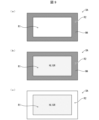
- FIG. (a) to (d) are plan views showing an example of a display device according to a second embodiment.
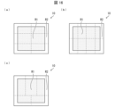
- 7 is a plan view showing an example of a display device of Embodiment 3.
- FIG. 7 is a plan view showing an example of a display device of Embodiment 4.
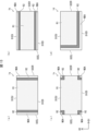
- FIGS. 1 to (c) are diagrams for explaining a method for manufacturing a display device according to a fifth embodiment, in which a variety of display devices can be obtained by changing the cutting position of the same mother substrate.
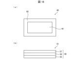
- . is a plan view showing a schematic configuration of a wavelength conversion layer included in a light emitting device of Embodiment 6, and (b) is a sectional view showing a schematic structure of the light emitting device of Embodiment 6. It is.
- (a) is a plan view showing a schematic configuration of a light emitting region provided in a lighting device according to Embodiment 7, and
- (b) is a sectional view showing a schematic configuration of a lighting device according to Embodiment 7. be.
- FIGS. 1 to 18 The embodiment of the present disclosure will be described below based on FIGS. 1 to 18.
- components having the same functions as those described in a specific embodiment will be denoted by the same reference numerals, and the description thereof may be omitted.
- FIG. 1 is a plan view showing a schematic configuration of a display device 1 according to the first embodiment.
- the display device 1 includes a display area DA including an upper end DAEU, a right end DAER, a lower end DAED, and a left end DAEL.
- a display area DA including an upper end DAEU, a right end DAER, a lower end DAED, and a left end DAEL.
- the shape of the display area DA can be determined as appropriate, and may be formed, for example, in an n-gon shape (n is a natural number of 3 or more) or in a circular shape.
- the display area DA When the display area DA is formed in an n-gonal shape (n is a natural number of 3 or more), the display area DA includes n edges (n is a natural number of 3 or more), and the display area DA is circular. , the display area DA includes one curved end.
- the display area DA of the display device 1 is equipped with a plurality of pixels PIX, and each pixel PIX includes a red sub-pixel RSP, a green sub-pixel GSP, and a blue sub-pixel BSP.
- each pixel PIX includes a red sub-pixel RSP, a green sub-pixel GSP, and a blue sub-pixel BSP.
- one pixel PIX is composed of a red sub-pixel RSP, a green sub-pixel GSP, and a blue sub-pixel BSP, but the invention is not limited to this.
- one pixel PIX may include sub-pixels of other colors in addition to the red sub-pixel RSP, the green sub-pixel GSP, and the blue sub-pixel BSP.
- the red sub-pixel RSP provided in the display area DA of the display device 1 includes a red light-emitting element that emits red light
- the green sub-pixel GSP provided in the display area DA of the display device 1 includes a green light-emitting element that emits green light
- the blue sub-pixel BSP provided in the display area DA of the display device 1 includes a blue light emitting element that emits blue light.
- the display area DA of the display device 1 includes a first area R1 including the entire center of the display area DA and a second area R2 including all edges of the display area DA, and the second area R2
- first area R1 including the entire center of the display area DA
- second area R2 including all edges of the display area DA
- the first region R1 is surrounded by a frame, but the present invention is not limited to this.
- the first area R1 only needs to include at least a part of the center of the display area DA
- the second area R2 only needs to include at least a part of the end of the display area DA.
- each of the red light emitting element, green light emitting element, and blue light emitting element provided in the first region R1 and the second region R2 of the display area DA is located between the first electrode and the second electrode.
- a nanoparticle layer containing nanoparticles mean particles (dots) with a maximum width of less than 1000 nm.
- the shape of the nanoparticles is not particularly limited as long as it satisfies the above-mentioned maximum width, and is not limited to a spherical three-dimensional shape (circular cross-sectional shape). For example, it may have a polygonal cross-sectional shape, a rod-like three-dimensional shape, a branch-like three-dimensional shape, a three-dimensional shape with an uneven surface, or a combination thereof.
- the concentration of halogen atoms contained in the nanoparticle layers provided in each of the red light emitting element, green light emitting element, and blue light emitting element provided in the first region R1 is the same as that in the second region R2.
- An example will be described in which the concentration of halogen atoms is higher than the concentration of halogen atoms contained in the nanoparticle layer provided in each of the red light-emitting element, green light-emitting element, and blue light-emitting element, but the present invention is not limited thereto.
- the concentration of halogen atoms contained in the nanoparticle layer provided in one or more light emitting elements (first light emitting element) among the red light emitting element, the green light emitting element, and the blue light emitting element provided in the first region R1. is the concentration of halogen atoms contained in the nanoparticle layer provided in one or more light emitting elements (second light emitting element) among the red light emitting element, the green light emitting element, and the blue light emitting element provided in the second region R2. It should be larger than .
- a light emitting element having a nanoparticle layer with a higher concentration of halogen atoms provided in the first region R1 and a nanoparticle layer with a lower concentration of halogen atoms provided in the second region R2 may be used.
- the light emitting element including the particle layer may be a light emitting element that emits the same color.
- a nanoparticle layer containing nanoparticles may be a charge transfer layer such as a hole injection layer, a hole transport layer, an electron injection layer, and an electron transport layer.
- a nanoparticle layer containing nanoparticles is a hole injection layer or a hole transport layer
- nanoparticles having a hole transporting property can be used as the nanoparticles
- nanoparticles having a hole transporting property can be used as the nanoparticles.
- NiO particles can be suitably used as the nanoparticle having hole transport properties.
- the nanoparticle layer containing nanoparticles is an electron injection layer or an electron transport layer
- nanoparticles having electron transporting properties can be used as the nanoparticles, and the nanoparticles having electron transporting properties are
- the nanoparticles contain at least one of Zn, Mg, Ti, Si, Sn, W, Ta, Ba, Zr, Al, Y, and Hf.
- ZnO particles may be used as nanoparticles having electron transport properties. It can be suitably used.
- the display device 1 includes a frame portion NDA. Since the frame portion NDA is a non-display area, no pixel PIX including sub-pixels of each color is provided.
- FIG. 2 is a cross-sectional view showing a schematic configuration of the first region R1 of the display area DA of the display device 1 of the first embodiment.
- the schematic configuration of the second area R2 of the display area DA of the display device 1 of the first embodiment is the same as the schematic configuration of the first area R1 shown in FIG.
- the concentration of halogen atoms contained in the nanoparticle layer provided in each of the red light-emitting element 5R, green light-emitting element 5G, and blue light-emitting element 5B provided in the second region R2 is different from that in the red light-emitting element, green light-emitting element, and blue light-emitting element provided in the second region R2.
- the difference is that the concentration is higher than the concentration of halogen atoms contained in the nanoparticle layer provided in each of the blue light emitting elements.
- a barrier layer 3 As shown in FIG. 2, in the display area DA of the display device 1, a barrier layer 3, a thin film transistor layer 4 including a transistor TR, a red light emitting element 5R, a green light emitting element 5G, and a blue light emitting element 5B are disposed on a substrate 12.
- a bank 23, a sealing layer 6, and a functional film 39 are provided in this order from the substrate 12 side.
- the blue sub-pixel BSP provided in the first region R1 of the display area DA of the display device 1 includes a blue light emitting element 5B, and the green sub-pixel GSP provided in the first region R1 of the display region DA of the display device 1 contains a green color.
- the red sub-pixel RSP which includes the light emitting element 5G and is provided in the first region R1 of the display area DA of the display device 1, includes the red light emitting element 5R.
- the substrate 12 may be, for example, a resin substrate made of a resin material such as polyimide, or a glass substrate.
- a resin substrate made of a resin material such as polyimide is used as the substrate 12 will be described as an example in order to make the display device 1 a flexible display device, but the present invention is not limited to this.
- a glass substrate can be used as the substrate 12.
- the barrier layer 3 is a layer that prevents foreign substances such as water and oxygen from entering the transistor TR, the red light emitting element 5R, the green light emitting element 5G, and the blue light emitting element 5B, and is made of, for example, silicon oxide formed by a CVD method. It can be formed of a silicon nitride film, a silicon oxynitride film, or a laminated film of these films.
- the transistor TR portion of the thin film transistor layer 4 including the transistor TR includes a semiconductor film SEM, doped semiconductor films SEM' and SEM'', an inorganic insulating film 16, a gate electrode G, an inorganic insulating film 18, and an inorganic insulating film. 20, a source electrode S, a drain electrode D, and a planarization film 21, and a portion other than the transistor TR portion of the thin film transistor layer 4 including the transistor TR includes an inorganic insulating film 16, an inorganic insulating film 18, and an inorganic insulating film 18. It includes a film 20 and a planarization film 21.
- the semiconductor films SEM, SEM', and SEM'' may be made of, for example, low-temperature polysilicon (LTPS) or an oxide semiconductor (for example, an In-Ga-Zn-O-based semiconductor).
- LTPS low-temperature polysilicon
- oxide semiconductor for example, an In-Ga-Zn-O-based semiconductor.
- the gate electrode G, source electrode S, and drain electrode D can be formed of a single-layer film or a laminated film of a metal containing at least one of aluminum, tungsten, molybdenum, tantalum, chromium, titanium, and copper, for example.
- the inorganic insulating film 16, the inorganic insulating film 18, and the inorganic insulating film 20 can be constituted by, for example, a silicon oxide film, a silicon nitride film, a silicon oxynitride film, or a stacked film thereof formed by a CVD method.
- the planarization film 21 can be made of a coatable organic material such as polyimide or acrylic, for example.
- the red light-emitting element 5R included in the red sub-pixel RSP includes an anode that is a first electrode 22 above the planarization film 21, a functional layer 24R that includes a red light-emitting layer, and a cathode that is a second electrode 25.
- the green light-emitting element 5G included in the green sub-pixel GSP includes an anode which is a first electrode 22 above the planarization film 21, a functional layer 24G including a green light-emitting layer, and a cathode which is a second electrode 25.
- the blue light emitting element 5B included in the blue subpixel BSP includes an anode which is a first electrode 22 above the planarization film 21, a functional layer 24B including a blue light emitting layer, and a cathode which is a second electrode 25. including.
- the insulating bank 23 covering the edge of the anode, which is the first electrode 22, can be formed by, for example, applying an organic material such as polyimide or acrylic and then patterning it by photolithography.
- the red light emitting element 5R which has a stack structure, includes a first electrode 22 that is an anode, and a second electrode 25 that is a cathode and is provided as a layer above the first electrode 22.
- the functional layer 24R including a red light emitting layer provided between the second electrode 25 which is a cathode includes, for example, a hole injection layer, a hole transport layer, a red light emitting layer, and an electron layer in order from the first electrode 22 side. It can be constructed by laminating a transport layer and an electron injection layer.
- the functional layers 24R including the red light emitting layer one or more of the hole injection layer, hole transport layer, electron transport layer, and electron injection layer other than the red light emitting layer may be omitted as appropriate.
- the green light emitting element 5G having a stack structure includes a first electrode 22 which is an anode and a second electrode 25 which is a cathode and is provided as an upper layer than the first electrode 22.
- the functional layer 24G including the green light emitting layer provided between the second electrode 25 which is the cathode includes, for example, a hole injection layer, a hole transport layer, a green light emitting layer, and an electron layer in order from the first electrode 22 side. It can be constructed by laminating a transport layer and an electron injection layer.
- the functional layers 24G including the green light emitting layer one or more of the hole injection layer, hole transport layer, electron transport layer, and electron injection layer other than the green light emitting layer may be omitted as appropriate.
- the blue light emitting element 5B having a stack structure includes a first electrode 22 which is an anode and a second electrode 25 which is a cathode and is provided as a layer above the first electrode 22.
- the functional layer 24B including a blue light emitting layer provided between the second electrode 25 which is a cathode includes, for example, a hole injection layer, a hole transport layer, a blue light emitting layer, and an electron layer in order from the first electrode 22 side. It can be constructed by laminating a transport layer and an electron injection layer.
- the functional layers 24B including the blue light emitting layer one or more of the hole injection layer, hole transport layer, electron transport layer, and electron injection layer other than the blue light emitting layer may be omitted as appropriate.
- the functional layer 24B including the blue light emitting layer is constructed by laminating a hole transport layer, a blue light emitting layer, and an electron transport layer in order from the anode side, which is the first electrode 22.
- the description will be given below, the invention is not limited thereto.
- a red light emitting element having an inverse product structure includes a first electrode as a cathode, a second electrode as an anode provided as a layer above the first electrode, and a second electrode as a cathode.
- the functional layer including the red light emitting layer provided between the first electrode and the second electrode, which is the anode includes, for example, an electron injection layer, an electron transport layer, a red light emitting layer, and a hole transport layer in order from the first electrode side. It can be constructed by laminating a layer and a hole injection layer.
- a green light emitting element having an inverse product structure includes a first electrode as a cathode and a second electrode as an anode provided as a layer above the first electrode, the first electrode as a cathode and the second electrode as an anode.
- the functional layer including the green light emitting layer provided between the second electrode and the second electrode is, for example, in order from the first electrode side: an electron injection layer, an electron transport layer, a green light emitting layer, a hole transport layer, and a hole injection layer. It can be constructed by laminating layers.
- a blue light emitting element having an inverse product structure includes a first electrode which is a cathode and a second electrode which is an anode provided as a layer above the first electrode.
- the functional layer including the blue light emitting layer provided between the second electrode and the second electrode may be, for example, in order from the first electrode side: an electron injection layer, an electron transport layer, a blue light emitting layer, a hole transport layer, and a hole injection layer. It can be constructed by laminating layers.
- the functional layers including the blue light emitting layer one or more layers other than the blue light emitting layer, such as an electron injection layer, an electron transport layer, a hole transport layer, and a hole injection layer, may be omitted as appropriate.
- the hole transport layer included in each of the functional layer 24R including the red light emitting layer, the functional layer 24G including the green light emitting layer, and the functional layer 24B including the blue light emitting layer does not contain nanoparticles, for example.
- N,N'-bis(4-butylphenyl)-N,N'-bis(phenyl)-benzidine (poly-TPD ) or polyvinylcarbazole (PVK) may also be used.
- the hole transport layer included in each of the functional layer 24R including the red light emitting layer, the functional layer 24G including the green light emitting layer, and the functional layer 24B including the blue light emitting layer has the above-mentioned hole transport properties. Nanoparticles may also be used.
- the electron transport layer included in each of the functional layer 24R including the red light emitting layer, the functional layer 24G including the green light emitting layer, and the functional layer 24B including the blue light emitting layer is made of, for example, a material that does not contain nanoparticles. This will be explained by taking as an example the case where 2,2',2''-(1,3,5-benzinetriyl)-tris(1-phenyl-1-H-benzimidazole) (TPBi) is used.
- TPBi 2,2',2''-(1,3,5-benzinetriyl)-tris(1-phenyl-1-H-benzimidazole)
- the present invention is not limited thereto, and nanoparticles having electron transport properties as described above may be used.
- each of the functional layer 24R including the red light-emitting layer, the functional layer 24G including the green light-emitting layer, and the functional layer 24B including the blue light-emitting layer is formed using the same material in the same process.
- An example will be described in which a hole transport layer and an electron transport layer formed using the same material and in the same process are provided, but the present invention is not limited thereto.
- each of the functional layer 24R including a red light emitting layer, the functional layer 24G including a green light emitting layer, and the functional layer 24B including a blue light emitting layer is the same as a hole injection layer formed in the same process using the same material. It may further include at least one of an electron injection layer formed using the same material in the same process.
- the respective hole transport layers included in each of the functional layers 24R, 24G, and 24B may be formed of mutually different materials.
- the hole transport layers included in each layer may be formed using the same material in the same process, and only the hole transport layer included in the remaining functional layer may be formed using a different material in a separate process.
- the respective electron transport layers included in each of the functional layers 24R, 24G, and 24B may be formed of different materials.
- each of the two functional layers of the functional layers 24R, 24G, and 24B The electron transport layers included in the functional layer may be formed using the same material in the same process, and only the electron transport layer included in the remaining functional layer may be formed using a different material in a separate process.
- the hole injection layers included in each of the functional layers 24R, 24G, and 24B may be formed of different materials.
- the hole injection layer included in each layer may be formed using the same material in the same process, and only the hole injection layer included in the remaining functional layer may be formed using a different material in a separate process.
- the respective electron injection layers included in each of the functional layers 24R, 24G, and 24B may be formed of different materials.
- each of the two functional layers of the functional layers 24R, 24G, and 24B The electron injection layer included in the functional layer may be formed using the same material in the same process, and only the electron injection layer included in the remaining functional layer may be formed using a different material in a separate process.
- the red light emitting element 5R, the green light emitting element 5G, and the blue light emitting element 5B are all QLEDs (quantum dot light emitting diodes), but the present invention is not limited to this. Instead, one or more of the red light emitting element 5R, the green light emitting element 5G, and the blue light emitting element 5B may be a QLED.
- the remaining two may be OLEDs (organic light emitting diodes); for example, the red light emitting element 5R , when two of the green light emitting element 5G and the blue light emitting element 5B are QLEDs, the remaining one may be an OLED.
- OLEDs organic light emitting diodes
- the hole injection layer, hole transport layer, electron transport layer, and electron injection layer other than each color light emitting layer among the functional layers 24R, 24G, and 24B including each color light emitting layer contains nanoparticles.
- the red light emitting element 5R, the green light emitting element 5G, and the blue light emitting element 5B may be an OLED (organic light emitting diode) having an organic light emitting layer that does not contain nanoparticles as a light emitting layer.
- the light emitting layer of each color light emitting element includes quantum dots.
- the quantum dots may have, for example, a core structure, a core/shell structure, a core/shell/shell structure, or a shell structure in which the core/shell ratio is continuously changed. Note that the shell may completely cover the core, or may partially cover the core.
- the core part can be composed of, for example, Si, C, etc.
- the core part in the case of a binary system, it can be composed of, for example, CdSe, CdS, CdTe, InP, GaP, InN, ZnSe, ZnS, ZnTe, etc.
- a ternary system it can be composed of, for example, CdSeTe, GaInP, ZnSeTe, etc.
- a quaternary system it can be composed of, for example, AIGS.
- the shell part can be composed of, for example, CdS, CdTe, CdSe, ZnS, ZnSe, ZnTe, etc.; in the case of a ternary system, it can be composed of, for example, CdSSe, CdTeSe, CdSTe, ZnSSe, ZnSTe, ZnTeSe, etc. , AIP, etc.
- quantum dots mean dots with a maximum width of 100 nm or less.
- the shape of the quantum dots is not particularly limited as long as it satisfies the above maximum width, and is not limited to a spherical three-dimensional shape (circular cross-sectional shape).
- it may have a polygonal cross-sectional shape, a rod-like three-dimensional shape, a branch-like three-dimensional shape, a three-dimensional shape with an uneven surface, or a combination thereof.
- a control circuit including a transistor TR that controls each of the red light emitting element 5R, the green light emitting element 5G, and the blue light emitting element 5B is a thin film transistor layer 4 including a transistor TR for each red subpixel RSP, green subpixel GSP, and blue subpixel BSP. It is set in. Note that the control circuit including the transistor TR provided for each of the red sub-pixel RSP, the green sub-pixel GSP, and the blue sub-pixel BSP and the light emitting element are also collectively referred to as a sub-pixel circuit.
- the red light emitting element 5R, green light emitting element 5G, and blue light emitting element 5B shown in FIG. 2 may be of a top emission type or a bottom emission type.
- the red light-emitting element 5R, the green light-emitting element 5G, and the blue light-emitting element 5B have a stacked structure in which the second electrode 25, which is a cathode, is arranged as an upper layer than the first electrode 22, which is an anode, so they are of top emission type.
- the first electrode 22, which is an anode may be formed of an electrode material that reflects visible light
- the second electrode 25, which is a cathode may be formed of an electrode material that transmits visible light, and in order to make it a bottom emission type.
- the first electrode 22 as an anode may be formed of an electrode material that transmits visible light
- the second electrode 25 as a cathode may be formed of an electrode material that reflects visible light.
- the red light emitting element, green light emitting element, and blue light emitting element have an inverse structure in which the second electrode, which is an anode, is arranged as an upper layer than the first electrode, which is a cathode, in order to make it a top emission type
- the first electrode, which is the cathode may be formed of an electrode material that reflects visible light
- the second electrode, which is the anode may be formed of an electrode material that transmits visible light.
- a certain first electrode may be formed of an electrode material that transmits visible light
- a second electrode, which is an anode may be formed of an electrode material that reflects visible light.
- the electrode material that reflects visible light is not particularly limited as long as it can reflect visible light and has conductivity, but for example, metal materials such as Al, Mg, Li, Ag, alloys of the above metal materials, or , a laminate of the metal material and a transparent metal oxide (for example, indium tin oxide, indium zinc oxide, indium gallium zinc oxide, etc.), or a laminate of the alloy and the transparent metal oxide, etc. .
- metal materials such as Al, Mg, Li, Ag, alloys of the above metal materials, or , a laminate of the metal material and a transparent metal oxide (for example, indium tin oxide, indium zinc oxide, indium gallium zinc oxide, etc.), or a laminate of the alloy and the transparent metal oxide, etc. .
- the electrode material that transmits visible light is not particularly limited as long as it can transmit visible light and has conductivity, but examples include transparent metal oxides (e.g., indium tin oxide, indium zinc oxide, indium gallium zinc oxide, etc.), a thin film made of a metal material such as Al or Ag, or a nanowire made of a metal material such as Al or Ag.
- transparent metal oxides e.g., indium tin oxide, indium zinc oxide, indium gallium zinc oxide, etc.
- a thin film made of a metal material such as Al or Ag
- a nanowire made of a metal material such as Al or Ag.
- a general electrode forming method can be used, such as a physical method such as a vacuum evaporation method, a sputtering method, an EB evaporation method, an ion plating method, etc. Examples include a vapor deposition (PVD) method and a chemical vapor deposition (CVD) method.
- the patterning method for the first electrode 22 and the second electrode 25 is not particularly limited as long as it can form a desired pattern with high precision, but specifically, photolithography, inkjet Laws, etc. can be mentioned.
- the sealing layer 6 is a light-transmitting film, and includes, for example, an inorganic sealing film 26 covering the second electrode 25, an organic film 27 above the inorganic sealing film 26, and an inorganic sealing film above the organic film 27. It can be configured with a stopping film 28.
- the sealing layer 6 prevents foreign substances such as water and oxygen from penetrating into the red light emitting element 5R, the green light emitting element 5G, and the blue light emitting element 5B.
- the inorganic sealing film 26 and the inorganic sealing film 28 are each inorganic films, and may be composed of, for example, a silicon oxide film, a silicon nitride film, a silicon oxynitride film, or a laminated film thereof formed by a CVD method. I can do it.
- the organic film 27 is a light-transmitting organic film that has a flattening effect, and can be made of a coatable organic material such as acrylic, for example.
- the organic film 27 may be formed by, for example, an inkjet method. In this embodiment, the case where the sealing layer 6 is formed of two layers of inorganic films and one layer of organic film provided between the two layers of inorganic films has been described as an example.
- the sealing layer 6 may be composed of only an inorganic film, only an organic film, one layer of an inorganic film and two layers of an organic film, or two or more layers. It may be composed of an inorganic film and two or more organic films.
- the functional film 39 is, for example, a film having at least one of an optical compensation function, a touch sensor function, and a protection function.
- FIG. 3 is a cross-sectional view showing a schematic configuration of the red light emitting element 5R provided in the first region R1 of the display area DA of the display device 1 of the first embodiment
- FIG. b is a sectional view showing a schematic configuration of a red light emitting element 5R' provided in a second region R2 of the display area DA of the display device 1 of the first embodiment.
- the green light emitting element 5G and the blue light emitting element 5B provided in the first region R1 of the display area DA of the display device 1 of Embodiment 1 are different from each other except that the light emitting colors of the light emitting layers are different.
- Each has the same configuration as the red light emitting element 5R' shown in FIG. 3(b) except that the emitted light color of the light emitting layer is different.
- the red light emitting element 5R shown in FIG. 3(a) is provided on the thin film transistor layer 4 including the transistor TR shown in FIG. 2, and includes a first electrode 22 as an anode, a second electrode 25 as a cathode, A functional layer 24R including a red light emitting layer is provided between the first electrode 22 and the second electrode 25.
- the functional layer 24R including the red light emitting layer has a structure in which a hole transport layer 24HT, a red light emitting layer 24REM, and an electron transport layer 24ET are laminated in order from the first electrode 22 side.
- the red light-emitting layer 24REM includes a ligand containing a halogen atom and a quantum dot.
- a ligand is a compound that has a coordinating function, and when both a ligand and a quantum dot are included, it can be considered that the ligand is coordinating with the quantum dot.
- the quantum dot QD shown in FIG. 3(a) means a quantum dot coordinated with a ligand containing a halogen atom.
- a ligand containing a halogen atom means a ligand containing a halogen atom, such as F , Cl , Br , and I. is attracted to the charged surface of the quantum dot. It is preferable that a ligand containing a halogen atom is coordinated with the quantum dot because stability and electron injection properties are improved, and among these, a ligand consisting of fluorine, which has a strong coordination force to the quantum dot, is more preferable. In this embodiment, an example will be described in which a fluorine ligand is used as a halogen atom-containing ligand in consideration of the strong coordination force to quantum dots, but the present invention is not limited to this. do not have.
- a ligand containing a halogen atom when used, for example, as in this embodiment, a ligand consisting of fluorine, which is a ligand consisting of a halogen atom, the length of the ligand is Since the length is short, aggregates QDA of quantum dots QD are likely to occur.
- the distance between quantum dots QD in the aggregate QDA of quantum dots QD is shorter than the distance between quantum dots QD in other than the aggregate QDA of quantum dots QD.
- the distance between quantum dots QD in an aggregate QDA of quantum dots QD is 1 nm or less, whereas the distance between quantum dots QD in other than the aggregate QDA of quantum dots QD is greater than 1 nm.
- the shape of the aggregate QDA of quantum dots QD is often spherical, but is not limited to this.
- the green light-emitting layer provided in the green light-emitting element 5G provided in the first region R1 of the display area DA of the display device 1 of Embodiment 1 includes quantum dots that emit green light and a ligand made of fluorine. Therefore, aggregates of quantum dots are likely to occur similarly to the red light emitting layer 24REM included in the red light emitting element 5R shown in FIG. 3(a).
- the blue light-emitting layer provided in the blue light-emitting element 5B provided in the first region R1 of the display area DA of the display device 1 of Embodiment 1 includes quantum dots that emit blue light and a ligand made of fluorine. Therefore, aggregates of quantum dots are likely to occur similarly to the red light emitting layer 24REM included in the red light emitting element 5R shown in FIG. 3(a).
- each of the red light emitting element 5R, the green light emitting element 5G, and the blue light emitting element 5B provided in the first region R1 of the display area DA of the display device 1 of the first embodiment has quantum dots formed by the ligand. Since it is strongly protected, high luminous efficiency can be achieved, but on the other hand, the light emitting element is likely to be destroyed at locations where quantum dot QD aggregates QDA are likely to occur and stress is likely to occur.
- the central part of the display area DA where stress is unlikely to occur is set as the first region R1, and each of the red light emitting element 5R, the green light emitting element 5G, and the blue light emitting element 5B is placed in the first region R1.
- the red light emitting element 5R' shown in FIG. 3(b) is provided on the thin film transistor layer 4 including the transistor TR shown in FIG. 2, and has a first electrode 22 as an anode and a second electrode 25 as a cathode. , and a functional layer including a red light emitting layer provided between the first electrode 22 and the second electrode 25.
- the functional layer including the red light emitting layer has a structure in which a hole transport layer 24HT, a red light emitting layer 24REM', and an electron transport layer 24ET are laminated in order from the first electrode 22 side.
- the red light emitting layer 24REM' includes an organic ligand and a quantum dot.
- the quantum dot QD' shown in FIG. 3(b) means a quantum dot coordinated with an organic ligand.
- An example of the organic ligand is, for example, an organic ligand made of organic molecules having a certain length in order to prevent quantum dots from aggregating with each other, but is not limited thereto.
- Examples of the organic ligand that can be used include, but are not limited to, oleylamine, oleic acid, dodecanethiol, trioctylphosphine, trioctylphosphine oxide, tributylphosphine oxide, and oleyl alcohol.
- red light-emitting layer 24REM' contains an organic ligand
- aggregation of quantum dots can be prevented, and quantum dots QDs as shown in FIG. 3(a) can be prevented from aggregating. Aggregated QDA is less likely to occur.
- the green light-emitting layer provided in the green light-emitting element provided in the second region R2 of the display area DA of the display device 1 of Embodiment 1 includes quantum dots that emit green light and an organic ligand. Therefore, like the red light emitting layer 24REM' provided in the red light emitting element 5R' shown in FIG. 3(b), aggregates of quantum dots are less likely to occur.
- the blue light emitting layer provided in the blue light emitting element provided in the second region R2 of the display area DA of the display device 1 of Embodiment 1 includes quantum dots that emit blue light and an organic ligand. Therefore, like the red light emitting layer 24REM' provided in the red light emitting element 5R' shown in FIG. 3(b), aggregates of quantum dots are less likely to occur.
- Each of the red light-emitting element 5R', the green light-emitting element, and the blue light-emitting element provided in the second region R2 of the display area DA of the display device 1 of Embodiment 1 includes an organic ligand.
- a region including the end of the display area DA where stress is likely to occur is defined as a second region R2, and a red light emitting element 5R' including a light emitting layer containing quantum dots and an organic ligand, By providing each of the green light emitting element and the blue light emitting element in the second region R2, damage to the light emitting elements is suppressed.
- the concentration of the quantum dot QD aggregate QDA which is a nanoparticle aggregate contained in the red light-emitting layer 24REM shown in (a) of FIG. This is higher than the concentration of aggregates of quantum dots QD' which are aggregates.
- each of the red light emitting element 5R, the green light emitting element 5G, and the blue light emitting element 5B provided in the first region R1 of the display area DA of the display device 1 has a light emitting layer containing a ligand made of fluorine.
- the red light emitting element 5R', the green light emitting element and the blue light emitting element provided in the second region R2 of the display area DA of the display device 1 each include a light emitting layer containing an organic ligand.
- the concentration of halogen atoms contained in the nanoparticle layer provided in the light emitting element (first light emitting element) provided in one region R1 is different from the concentration of halogen atoms contained in the nanoparticle layer provided in the light emitting element provided in the second region R2 (second light emitting element).
- the concentration is set to be higher than the concentration of halogen atoms contained in the nanoparticle layer, the present invention is not limited to this.
- each of the red light emitting element 5R, the green light emitting element 5G, and the blue light emitting element 5B provided in the first region R1 of the display area DA of the display device 1 includes both a fluorine ligand and an organic ligand.
- Each of the red light-emitting element 5R', the green light-emitting element, and the blue light-emitting element provided with a light-emitting layer and provided in the second region R2 of the display area DA of the display device 1 contains both a fluorine-containing ligand and an organic ligand.
- concentration of halogen atoms means the number of halogen atoms contained per certain volume, and can be calculated from, for example, the results of SEM-EDX measurement of a cross section of the light emitting layer.
- 4(a) and 4(b) show the aggregate QDA of quantum dots QD of the red light emitting element 5R provided in the first region R1 of the display area DA of the display device 1 of the first embodiment. It is a figure showing an example of the phenomenon which may occur in the periphery.
- the electron transport layer 24ET provided directly above the red light emitting layer 24REM, that is, the electron transport layer 24ET provided as a layer immediately above the red light emitting layer 24REM and in contact with the red light emitting layer 24REM,
- the electron transport layer 24ET may be formed with a protrusion 24ETP that penetrates into the red light emitting layer 24REM, which is a layer of the electron transport layer 24ET.
- the unit length of the red light-emitting layer 24REM means the width of a cross-sectional view of the red light-emitting element 5R taken with a scanning electron microscope (SEM) at a magnification that allows easy observation of the number of penetrations described above, and is, for example, 600 nm or more. , 1000 nm or less.
- SEM scanning electron microscope
- the thickness of the maximum film thickness of the red light emitting layer 24REM is the thickness of the red light emitting layer 24REM in a cross-sectional view of the red light emitting element 5R taken with a scanning electron microscope (SEM) at a magnification that allows easy observation of the number of penetrations described above. means the maximum thickness of the red light emitting layer 24REM in the direction perpendicular to the unit length of .
- the red light emitting layer 24REM is observed to have a substantially uniform thickness.
- the substantially uniform thickness of the red light emitting layer 24REM can be regarded as the thickness of the maximum thickness portion of the red light emitting layer 24REM.
- the central position of the maximum thickness portion means a position where the maximum thickness portion is divided into two parts each having a thickness that is half the thickness of the maximum thickness portion.
- the fact that the electron transport layer 24ET has entered below the reference position L3 of the red light emitting layer 24REM means that the protrusion 24ETP of the electron transport layer 24ET is formed in the region between the reference position L3 of the red light emitting layer 24REM and the hole transport layer 24HT. means that it has been
- the red light emitting layer 24REM' of the red light emitting element 5R' provided in the second region R2 of the display area DA of the display device 1 aggregates of quantum dots QD' has not occurred.
- the center position of the maximum thickness part of the red light emitting layer 24REM' is set as the reference position L1 shown in FIG.
- the layer 24ET that is, the electron transport layer 24ET, which is in contact with the red light emitting layer 24REM' and is provided as a layer immediately above the red light emitting layer 24REM', is below the reference position L1 of the red light emitting layer 24REM', which is the layer below.
- the unit length of the red light emitting layer 24REM' is preferably set to be the same as the unit length of the red light emitting layer 24REM described above.
- the thickness of the maximum film thickness portion of the red light emitting layer 24REM' is the scanning of the red light emitting element 5R' taken with the unit length of the red light emitting layer 24REM' set to be the same as the unit length of the red light emitting layer 24REM. In a cross-sectional view of an electron microscope (SEM), it means the maximum thickness of the red light emitting layer 24REM' in a direction perpendicular to the unit length of the red light emitting layer 24REM'.
- SEM electron microscope
- red light emission is When the layer 24REM' is observed to have a substantially uniform thickness, the substantially uniform thickness of the red light emitting layer 24REM' can be regarded as the thickness of the maximum thickness portion of the red light emitting layer 24REM'.
- the fact that the electron transport layer 24ET has entered below the reference position L1 of the red light emitting layer 24REM' means that the protrusion 24ETP of the electron transport layer 24ET is in the area between the reference position L1 of the red light emitting layer 24REM' and the hole transport layer 24HT. This means that it has been formed up to.
- the quantum dots QD are Aggregate QDA is likely to occur.
- quantum dots are placed in the electron transport layer 24ET provided directly above the red light emitting layer 24REM, that is, in the electron transport layer 24ET provided as a layer immediately above the red light emitting layer 24REM and in contact with the red light emitting layer 24REM.
- the aggregate QDA of quantum dots QD included in the red light emitting layer 24REM may be formed so that the protrusion QDAP of the aggregate QDA of QDs enters. If the center position of the maximum thickness portion of the electron transport layer 24ET is the reference position L4 shown in FIG. When counted per unit length of the red light emitting layer 24REM, it is 1.
- the thickness of the maximum film thickness portion of the electron transport layer 24ET is defined as the thickness of the red light emitting layer 24REM in a cross-sectional view of the red light emitting element 5R taken with a scanning electron microscope (SEM) at a magnification sufficient to easily observe the number of penetrations described above. means the maximum thickness of the electron transport layer 24ET in the direction perpendicular to the unit length of .
- the electron transport layer 24ET is observed to have a substantially uniform thickness.
- the substantially uniform thickness of the electron transport layer 24ET can be regarded as the thickness of the maximum thickness portion of the electron transport layer 24ET.
- the red light-emitting layer 24REM has entered the electron transport layer 24ET at or above the reference position L4, which means that the protrusion QDAP of the aggregate QDA of quantum dots QD is in the area between the reference position L4 of the electron transport layer 24ET and the second electrode 25. This means that it has been formed up to.
- the unit length of the red light emitting layer 24REM' is preferably set to be the same as the unit length of the red light emitting layer 24REM described above.
- the thickness of the maximum film thickness portion of the electron transport layer 24ET is the scanning type of the red light emitting element 5R' photographed with the unit length of the red light emitting layer 24REM' set to be the same as the unit length of the red light emitting layer 24REM. In a cross-sectional view of an electron microscope (SEM), it means the maximum thickness of the electron transport layer 24ET in the direction orthogonal to the unit length of the red light emitting layer 24REM'.
- the fact that the red light emitting layer 24REM' has entered the reference position L2 or more of the electron transport layer 24ET means that the protrusion QDAP of the aggregate QDA of quantum dots QD is in the area between the reference position L2 of the electron transport layer 24ET and the second electrode 25. This means that it is formed up to .
- the concentration of halogen atoms contained in the first layer, which is the nanoparticle layer, of the first light emitting element provided in the first region R1 of the display area DA of the display device 1 is , higher than the concentration of halogen atoms contained in the second layer, which is a nanoparticle layer, of the second light emitting element provided in the second region R2 of the display area DA of the display device 1, and Since the second light emitting element has a stacked stack structure, the first layer and the second layer are light emitting layers containing quantum dots, and the third layer formed directly above the first layer and the second layer are light emitting layers containing quantum dots.
- the fourth layer formed directly above the second layer is an electron transport layer
- the fourth layer is not limited to this, and the fourth layer formed immediately above the first layer is an electron transport layer.
- the third layer and the fourth layer formed directly above the second layer may be electron injection layers.
- the layer may be a hole transport layer or a hole injection layer.
- the first layer and the second layer are hole transport layers, and are formed directly on the first layer.
- the third layer and the fourth layer formed directly above the second layer may be light emitting layers.
- the first layer and the second layer are hole transport layers, and the first layer and the second layer are hole transport layers, and the first layer and the second layer are hole transport layers.
- the third layer formed and the fourth layer formed immediately above the second layer may be either the first electrode or the second electrode, which is a hole injection layer or an electrode layer.
- the first layer and the second layer are electron transport layers, and are formed directly on the first layer.
- the third layer and the fourth layer formed directly above the second layer may be either an electron injection layer or an electrode layer, which is the first electrode and the second electrode.
- the first layer and the second layer are electron transport layers, and are formed directly on the first layer.
- the third layer formed directly above the second layer and the fourth layer formed directly above the second layer may be light emitting layers.
- the first layer and the second layer are hole injection layers, and are formed directly on the first layer.
- the third layer and the fourth layer formed directly above the second layer may be either the first electrode or the second electrode, which are electrode layers.
- the first layer and the second layer are electron injection layers, and are formed directly above the first layer.
- the third layer and the fourth layer formed directly above the second layer may be either the first electrode or the second electrode, which are electrode layers.
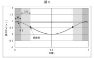
- FIG. 5 is a diagram for explaining the deflection due to its own weight of the substrate 12 provided in the display device 1 of the first embodiment.
- the deflection ⁇ (x) of the substrate 12 at position x due to a uniformly distributed load (assuming the substrate's own weight) when both ends of the substrate 12 of length L are held is given by the following formula.
- q is the load per unit length applied to the substrate 12 (proportional to the substrate density)
- E is the Young's modulus of the substrate 12
- I is the second moment of area of the substrate 12.
- the displacement D(x) of the substrate 12 is expressed by the following formula. However, 1 in the first term and 0.54 in the second term are normalization constants.
- the second region R2 of the display area DA shown in FIG. A region (third region) formed with a larger width of 9% or less, and a region in the second direction D2 of the substrate 12 from each of the two ends D1EU and D1ED of the substrate 12 formed along the first direction D1. It is preferable that the fourth region be provided in at least one of a region (fourth region) formed with a width greater than 0% and less than 9% of the length.
- the second region R2 of the display area DA shown in FIG. A region (third region) formed with a width greater than 9% and less than or equal to 21%, and a second direction of the substrate 12 from each of the two ends D1EU and D1ED of the substrate 12 formed along the first direction D1. It is more preferable that the fourth region be provided in at least one of a region (fourth region) formed with a width greater than 9% and less than 21% of the length of D2.
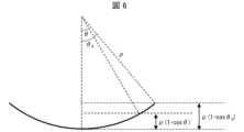
- FIG. 6 is a diagram for explaining the substrate 12 included in the display device 1 of Embodiment 1 and locations where stress is likely to occur when a layer having a different coefficient of thermal expansion from the substrate 12 is provided on the substrate 12. be.
- the substrate 12 and each layer provided on the substrate 12 have different coefficients of thermal expansion, so that heating produces stress.
- a first thin plate having a thickness h 1 , a Young's modulus E 1 and a coefficient of thermal expansion ⁇ 1 and a second thin plate having a thickness h 2 , a Young's modulus E 2 and a coefficient of thermal expansion ⁇ 2 are in contact with the substrate 12.
- the radius of curvature ⁇ of deformation due to temperature rise ⁇ T is given by the following formula.
- h h 1 +h 2
- m E 1 /E 2
- n h 1 /h 2 .
- the second region R2 of the display area DA shown in FIG. A region (third region) formed with a larger width of 3% or less, and a region in the second direction D2 of the substrate 12 from each of the two ends D1EU and D1ED of the substrate 12 formed along the first direction D1. It is preferable that the fourth region be provided in at least one of a region (fourth region) formed with a width of more than 0% and less than 3% of the length.
- the second region R2 of the display area DA shown in FIG. A region (third region) formed with a width greater than 3% and less than or equal to 15%, and a second direction of the substrate 12 from each of two end portions D1EU and D1ED of the substrate 12 formed along the first direction D1. More preferably, it is provided in at least one of a region (fourth region) formed with a width greater than 3% and less than 15% of the length of D2.
- the second region R2 of the display area DA shown in FIG. A region (third region) formed with a width of 3% or more and 15% or less, and a second direction D2 of the substrate 12 from each of two end portions D1EU and D1ED of the substrate 12 formed along the first direction D1. Most preferably, it is provided in at least one of a region (fourth region) formed with a width of 3% or more and 15% or less of the length of.
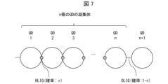
- FIG. 7 is a diagram for explaining the coverage rate of quantum dots with the halogen ligand HLIG in the light emitting layer provided in the light emitting element included in each subpixel of the display device 1 of Embodiment 1.
- the area of the halogen ligand HLIG indicating the coverage rate of the quantum dot with the halogen ligand HLIG/the surface area of the quantum dot is defined as r.
- An organic ligand OLIG can be used to prevent quantum dots from aggregating. As shown in FIG. 7, the organic ligand OLIG exists in a portion 1-r of the surface area of the quantum dot where the halogen ligand HLIG is not present.
- the average number of quantum dots (expected value of n) E in the one-dimensional aggregate of n quantum dots shown in FIG. 7 is given by the following formula.
- the size of the quantum dot aggregates will be , is smaller than the thickness of the light emitting layer. That is, if E ⁇ 3 and r ⁇ 0.67, the size of the quantum dot aggregate is smaller than the thickness of the light-emitting layer, so that the device is less likely to break due to stress.
- the quantum The light-emitting layer including dots can be configured to be substantially flat, and problems with device characteristics are less likely to occur.
- the coverage rate of nanoparticles with halogen atoms in the first region R1 of the display area DA is 67% or more and 80% or less
- the coverage rate of nanoparticles with halogen atoms in the second region R2 of the display area DA is 67% or more and 80% or less. , preferably 0% or more and less than 67%.
- r which is (area of halogen ligand HLIG/surface area of quantum dot), can be determined as follows, for example, from the cross-sectional SEM-EDX results (number of halogens per unit volume N).
- r number of halogens per unit volume N ⁇ volume of quantum dot ⁇ area occupied by one halogen atom/surface area of quantum dot, that is, r can be determined as shown below.
- d Q is the diameter of the quantum dot
- d h is twice the ionic radius of the halide ion
- the ionic radius is 0.13 nm in the case of F.
- red light emitting layer forming step of forming the red light emitting layer 24REM' a green light emitting layer forming step of forming the green light emitting layer 24GEM', and a blue light emitting layer forming step of forming the blue light emitting layer BEM' will be described. The process will be explained.
- FIGS. 8(a) to 8(o) illustrate lift-off of the quantum dot layer, which is part of the process of forming a light emitting layer provided in a light emitting element included in each subpixel of the display device 1 of Embodiment 1. It is a figure which shows an example of the process of forming by the method. Note that in FIGS. 8(a) to 8(o), illustration of the first electrodes 22 provided in the light emitting elements of each color is omitted.
- the patterning process of the red light-emitting layer 24REM', the green light-emitting layer 24GEM', and the blue light-emitting layer 24BEM' using the lift-off method includes forming the first photosensitive resin layer 40A on the hole transport layer 24HT shown in FIG. 8(a). a step of exposing the first photosensitive resin layer 40A through the mask M1 shown in FIG. 8(b), and a step of forming an opening in the first photosensitive resin layer 40A (FIG. 8(c)). A step of developing using a developer shown in FIG. The step of removing the first photosensitive resin layer 40A using the resist removing liquid shown in FIG.
- the patterning process of the red light emitting layer 24REM', the green light emitting layer 24GEM', and the blue light emitting layer 24BEM' using the lift-off method further includes patterning the red light emitting layer 24REM' and the hole transport layer 24HT shown in FIG. 8(f). a step of forming a second photosensitive resin layer 40B, a step of exposing the second photosensitive resin layer 40B through a mask M2 shown in FIG. A step of developing using a developer shown in (h) of FIG. 8, and a step of applying and heat-treating a solution containing green light-emitting quantum dots shown in (i) of FIG. 8 to obtain a green light-emitting layer 24GEM'.
- the patterning process of the red light-emitting layer 24REM', the green light-emitting layer 24GEM', and the blue light-emitting layer 24BEM' using the lift-off method further includes the patterning process of the red light-emitting layer 24REM', the green light-emitting layer 24GEM', as shown in FIG. 8(k). and a step of forming a third photosensitive resin layer 40C on the hole transport layer 24HT, a step of exposing the third photosensitive resin layer 40C through a mask M3 shown in (l) of FIG.
- the method includes a step of obtaining a layer 24BEM', and a step of removing the third photosensitive resin layer 40C using a resist removal liquid shown in FIG. 8(o) to obtain a patterned blue light emitting layer 24BEM'.
- the resist removal liquid shown in FIG. 8(e), FIG. 8(j), and FIG. 8(o) for example, PGMEA etc. can be used, but it is not limited to this. .
- the red light emitting layer 24REM', the green light emitting layer 24GEM', and the blue light emitting layer 24BEM' are formed in this order has been described as an example, but the present invention is not limited to this.
- the light emitting layer of any color may be formed first.
- FIGS. 9(a) to 9(c) are diagrams illustrating an example of the process of incorporating the halogen ligand HLIG only into the first region R1 of the display area DA of the display device 1 of the first embodiment.
- a mask M4 having an opening in a region corresponding to the first region R1 of the display area DA and a light shielding portion in a region corresponding to the second region R2 of the display area DA, A red light-emitting layer 24REM', a green light-emitting layer 24GEM', and a blue light-emitting layer 24BEM' shown in FIG. 8(o) are placed on a substrate.
- the halogen ligand HLIG is applied only to the first region R1, which is the center of the display area DA.
- a region HLIGR with a high concentration of can be formed.
- the solution containing the halogen ligand HLIG at least a portion of the organic ligand OLIG in the first region R1, which is the center of the display area DA, may be removed with an alcohol solution, if necessary. .
- the alcohol solution for example, methanol or ethanol can be suitably used, but the solution is not limited thereto.
- the concentration of halogen atoms contained in each of the red light emitting layer 24REM, the green light emitting layer, and the blue light emitting layer provided in the first region R1 is increased.
- the concentration of halogen atoms can be made higher than the concentration of halogen atoms contained in each of the red light emitting layer 24REM', the green light emitting layer 24GEM', and the blue light emitting layer 24BEM' provided in the second region R2.
- FIGS. 10(a) to 10(d) are diagrams showing another example of the process of introducing the halogen ligand HLIG only into the first region R1 of the display area DA of the display device 1 of the first embodiment. .
- the fourth photosensitive resin layer 40D is formed by a red light-emitting layer 24REM', a green light-emitting layer 24GEM', and a blue light-emitting layer 24BEM' shown in (o) of FIG. It is formed on the entire surface of the substrate.
- the fourth photosensitive resin layer 40D is patterned by exposure using a mask (not shown) and development, and the first region R1 of the display area DA is An opening can be formed in a region corresponding to.
- a solution containing the halogen ligand HLIG is applied with the fourth photosensitive resin layer 40D having an opening formed in the region corresponding to the first region R1 of the display area DA.
- a region HLIGR with a high concentration of halogen ligand HLIG can be formed only in the first region R1, which is the central portion of the display area DA.
- the solution containing the halogen ligand HLIG at least a portion of the organic ligand OLIG in the first region R1, which is the center of the display area DA, may be removed with an alcohol solution, if necessary. .
- the alcohol solution for example, methanol or ethanol can be suitably used, but the solution is not limited thereto.
- the red light-emitting layer 24REM, the green light-emitting layer, and the blue light-emitting layer provided in the first region R1 are removed.
- the concentration of halogen atoms contained in each of the red light emitting layer 24REM', the green light emitting layer 24GEM', and the blue light emitting layer 24BEM' provided in the second region R2 can be made higher than the concentration of halogen atoms contained in each of the red light emitting layer 24REM', the green light emitting layer 24GEM', and the blue light emitting layer 24BEM' provided in the second region R2.
- FIG. 11 is a diagram showing the image signal converter 45, sub-pixel circuit SPDR, and various wirings included in the display device 1 of the first embodiment.
- FIG. 12 is a diagram illustrating an example of the sub-pixel circuit SPDR included in the display device 1 of Embodiment 1.
- the sub-pixel circuit SPDR (n, n) includes, for example, a transistor Tr1, a transistor Tr2, and a capacitor C1.
- the transistor Tr1 is a drive transistor (for example, the transistor TR of the thin film transistor layer 4 shown in FIG. 2) that drives the red light emitting element 5R'.
- the source electrode of the transistor Tr1 is connected to the power supply line PLn to which a first level (for example, high level) voltage is applied, and the gate electrode of the transistor Tr1 is connected to the drain electrode of the transistor Tr2 and one terminal of the capacitor C1.
- the drain electrode of the transistor Tr1 is connected to the anode electrode of the red light emitting element 5R'.
- the transistor Tr2 is a selection transistor that selects a light emitting element to emit light according to a scan signal supplied from the scan line SCLn.
- the source electrode of the transistor Tr2 is connected to the signal line SLn
- the gate electrode of the transistor Tr2 is connected to the scanning line SCLn
- the drain electrode of the transistor Tr2 is connected to the gate electrode of the transistor Tr1 and one terminal of the capacitor C1. ing.
- the cathode electrode of the red light emitting element 5R' opposite to the anode electrode connected to the transistor Tr1 and the other terminal of the capacitor C1 opposite to one terminal are at the second level (for example, low level). It is grounded by being connected to the GND line to which voltage is applied.
- the transistor Tr2 is turned on by supplying the scanning signal from the scanning line SCLn to the transistor Tr2, and at the same time, the image signal converter 45 shown in FIG. 11 supplies data signals to the signal lines SL1 to SLn, and the transistor Tr2 is turned on.
- the signal is transmitted to the transistor Tr1 via the transistor Tr1.
- a current corresponding to the data signal flows through the light emitting elements provided in each sub-pixel circuit SPDR(1,1) to SPDR(n, n+1), so that the light emitting elements emit light.
- the concentration of halogen atoms contained in each of the red light-emitting layer 24REM, the green light-emitting layer, and the blue light-emitting layer provided in the first region R1 is the same as that in the second region R2. Since the concentration of halogen atoms contained in each of the red light-emitting layer 24REM', the green light-emitting layer 24GEM', and the blue light-emitting layer 24BEM' is higher than the concentration of halogen atoms, the device characteristics of the first light-emitting element provided in the first region R1 and the second region The device characteristics of the second light emitting device provided in R2 are different.
- the luminous efficiency of the first light emitting element is the first. Since the luminous efficiency is higher than that of the two light emitting elements, the drive current corresponding to the same brightness is smaller in the first light emitting element than in the second light emitting element.
- the display device 1 of this embodiment includes an image signal converter 45 shown in FIG. 11.
- the image signal conversion unit 45 converts a first data signal regarding the drive current of the first light emitting element based on the first coefficient and supplies it to the first light emitting element, and converts the first data signal regarding the drive current of the second light emitting element into a second data signal regarding the drive current of the second light emitting element. is converted based on the second coefficient and supplied to the second light emitting element.
- the display area DA includes a first area R1 and a second area R2, and the second area R2 surrounds the first area R1 in a frame shape.
- the invention is not limited to this.
- the second region R2 surrounding the first region R1 in a frame shape may further include n (n is a natural number of 2 or more) frame-shaped regions. For example, if n is 2 and the second region R2 surrounding the first region R1 in a frame shape is composed of two frame-shaped regions, the second region R2 is a frame closer to the first region R1.
- the first second region has a shape and a second second region has a frame shape that is farther from the first region R1, and is provided in a second light emitting element provided in the first second region.
- the concentration of halogen atoms contained in the nanoparticle layer may be higher than the concentration of halogen atoms contained in the nanoparticle layer provided in the second light emitting element provided in the second second region.
- the shape of the first region R1 includes at least a part of the center of the display area DA, and the second region includes at least a part of the end of the display area DA.
- the display device 1 is different from the display device 1 described in the first embodiment in that the shape of R2 is different.
- Other details are as described in the first embodiment. For convenience of explanation, members having the same functions as those shown in the drawings of Embodiment 1 are given the same reference numerals, and the explanation thereof will be omitted.
- FIGS. 13(a) to 13(d) are plan views showing examples of display devices 1a, 1b, 1c, and 1d of the second embodiment.
- the display device 1a has a length in a first direction D1, which is a longitudinal direction, and a length in a second direction D2, which is perpendicular to the first direction D1, and has a display area. It includes a substrate 12 having a DA and a frame portion NDA.
- the frame portion NDA is provided along the second direction D2 closer to each of the two end portions D2EL and D2ER of the substrate 12 formed along the second direction D2 than the second region R2.
- the display device 1a is provided with the frame portion NDA has been described as an example, but the present invention is not limited to this, and the display device 1a may not include the frame portion NDA.
- a second region R2 may be provided instead of the frame portion NDA.
- the display device 1a since the frame portion NDA is present only on the short side of the display device 1a, the area of the frame portion NDA can be reduced compared to the case where the frame portion NDA is provided on the long side of the display device 1a. Therefore, a larger display area DA can be secured.
- the display device 1a when the frame portion NDA is not provided and the second region R2 is provided instead of the frame portion NDA, a display area DA of an even larger size can be secured.
- the display device 1b has a length in a first direction D1, which is a longitudinal direction, and a length in a second direction D2, which is orthogonal to the first direction D1, and has a display area. It includes a substrate 12 having a DA and a frame portion NDA.
- the frame portion NDA is provided along the first direction D1 closer to each of the two end portions D1EU and D1ED of the substrate 12 formed along the first direction D1 than the second region R2.
- the display device 1b is provided with the frame portion NDA has been described as an example, but the present invention is not limited to this, and the display device 1b may be provided without the frame portion NDA.
- a second region R2 may be provided instead of the frame portion NDA.
- the display device 1b by holding the long sides of the display device 1b, stress due to its own weight can be reduced even if it is a large display.
- the display device 1b if the frame portion NDA is not provided and the second region R2 is provided instead of the frame portion NDA, a display area DA of an even larger size can be secured.
- the display device 1c has a length in a first direction D1, which is a longitudinal direction, and a length in a second direction D2, which is perpendicular to the first direction D1, and has a display area. It includes a substrate 12 having a DA and a frame portion NDA.
- the frame portion NDA is a frame portion 4 where two end portions D1EU and D1ED of the substrate 12 formed along the first direction D1 are in contact with two end portions D2EL and D2ER of the substrate 12 formed along the second direction D2. It is provided at one corner, and is provided closer to the corner than the second region R2.
- the frame portion NDA may be provided only at at least two corners farthest from each other among the four corners. Further, in the present embodiment, the case where the display device 1c is provided with the frame portion NDA has been described as an example, but the present invention is not limited to this, and the display device 1c may not be provided with the frame portion NDA. Alternatively, the second region R2 may be provided only at the four corners or the two corners.
- the frame portions NDA are provided only at the four corners or the two corners, the area of the frame portions NDA can be reduced, so that a larger display area DA can be secured. I can do it.
- the display device 1c when the second region R2 is provided only at the four corners or the two corners without providing the frame portion NDA, a display area DA of an even larger size can be secured. I can do it.
- the display device 1d has a length in a first direction D1, which is a longitudinal direction, and a length in a second direction D2, which is perpendicular to the first direction D1, and has a display area. It includes a substrate 12 having a DA and a frame portion NDA.
- the frame portion NDA is provided at the end portions D1ED and D2EL of the substrate 12 where the second region R2 is provided, and at the end portions D1ED and D2EL of the substrate 12 than the second region R2.
- the frame portion NDA includes a portion formed along the first direction D1 near one of the two end portions D1EU and D1ED of the substrate 12 formed along the first direction D1, and a second portion formed along the first direction D1. It may be formed so as to include a portion formed along the second direction D2 near one of the two end portions D2EL and D2ER of the substrate 12 formed along the direction D2.
- the display device 1d is provided with the frame portion NDA
- the display device 1d is not limited to this, and the display device 1d is not provided with the frame portion NDA. It's okay.
- the second region R2 is located at one of the two ends D1EU and D1ED of the substrate 12 formed along the first direction D1.
- the frame portion NDA is provided on two sides including one corner, the area of the frame portion NDA can be reduced, and a larger display area DA can be secured.
- the display device 1d when the frame portion NDA is not provided and the second region R2 is provided on two sides including one corner, an even larger display area DA can be secured.
- the frame portion NDA is located between (1) two end portions D2EL and D2ER of the substrate 12 formed along the second direction D2; (2) a second frame area along the first direction D1 including two ends D1EU and D1ED of the substrate 12 formed along the first direction D1; , (3) Four edges where the two ends D1EU and D1ED of the substrate 12 formed along the first direction D1 and the two ends D2EL and D2ER of the substrate 12 formed along the second direction D2 are in contact with each other.
- the corners at least the two corners farthest from each other are the third frame area, and (4) the two ends D1EU and D1ED of the substrate 12 formed along the first direction D1. and a portion formed along the first direction D1 including one of the two ends D2EL and D2ER of the substrate 12 formed along the second direction D2. and a fourth frame area including a portion formed along the fourth frame area.
- the first light emitting element provided in the first region R1 is included in the first sub-pixel
- the second light emitting element provided in the second region R2 is included in the second sub-pixel.
- the light-emitting layer, which is a nanoparticle layer containing nanoparticles, of the first sub-pixel and the light-emitting layer, which is a nanoparticle layer containing nanoparticles, of the second sub-pixel are respectively arranged in an inner region SPCR/SPCR' and an outer region.
- the inner regions SPCR and SPCR' have a higher concentration of halogen atoms than the outer regions SPER and SPER', and the first sub-pixel has a higher concentration of halogen atoms than the second sub-pixel.
- This is different from the display devices described in Embodiments 1 and 2 in that the area of the inner regions SPCR and SPCR' occupies a high proportion of the area.
- the other details are as described in the first and second embodiments. For convenience of explanation, members having the same functions as those shown in the drawings of Embodiments 1 and 2 are given the same reference numerals, and their explanations are omitted.
- FIG. 14 is a plan view showing an example of the display device 1e of Embodiment 3.
- the first light emitting element provided in the first region R1 is included in the first sub-pixel
- the second light emitting element provided in the second region R2 is included in the second sub-pixel.
- a light-emitting layer that is a nanoparticle layer that is included in a pixel and includes nanoparticles of the first sub-pixel and a light-emitting layer that is a nanoparticle layer that includes nanoparticles of the second sub-pixel are in inner regions SPCR and SPCR', respectively.
- the inner regions SPCR/SPCR' have a higher concentration of halogen atoms than the outer regions SPER/SPER', and the first sub-pixel has a higher concentration of halogen atoms than the second sub-pixel,
- the area of the inner regions SPCR and SPCR' occupies a high proportion of the area of the sub-pixel.
- concentration of halogen atoms contained in the nanoparticle layer provided in one or more light emitting elements (second light emitting element) of the red light emitting element, the green light emitting element, and the blue light emitting element provided in the second region R2 It is higher than the concentration of halogen atoms contained.
- the second region R2 is provided with two or more second sub-pixels including the second light emitting element, and among the two or more second sub-pixels, the second sub-pixel is closer to the first region R1.
- the concentration of halogen atoms contained in the nanoparticle layer of the second sub-pixel located in the second sub-pixel is higher than that of the nanoparticles in the second sub-pixel located farther from the first region R1 among the two or more second sub-pixels.
- the concentration may be greater than the concentration of halogen atoms contained in the layer.
- the first light emitting element provided in the first region R1 is included in the first sub-pixel
- the second light emitting element provided in the second region R2 is included in the second sub-pixel.
- the light-emitting layer, which is a nanoparticle layer containing nanoparticles, of the first sub-pixel and the light-emitting layer, which is a nanoparticle layer containing nanoparticles, of the second sub-pixel are respectively arranged in an inner region SPCR/SPCR' and an outer region.
- the outer regions SPER and SPER' have a higher concentration of halogen atoms than the inner regions SPCR and SPCR', and the first sub-pixel has a higher concentration of halogen atoms than the second sub-pixel.
- This differs from the display devices described in Embodiments 1 to 3 in that the area of the outer regions SPER and SPER' occupies a high proportion of the area.
- Other details are as described in Embodiments 1 to 3. For convenience of explanation, members having the same functions as those shown in the drawings of Embodiments 1 to 3 are given the same reference numerals, and their explanations are omitted.
- FIG. 15 is a plan view showing an example of the display device 1f of Embodiment 4.
- the first light emitting element provided in the first region R1 is included in the first sub-pixel
- the second light emitting element provided in the second region R2 is included in the second sub-pixel.
- a light-emitting layer that is a nanoparticle layer that is included in a pixel and includes nanoparticles of the first sub-pixel and a light-emitting layer that is a nanoparticle layer that includes nanoparticles of the second sub-pixel are in inner regions SPCR and SPCR', respectively.
- the outer regions SPER/SPER' have a higher concentration of halogen atoms than the inner regions SPCR/SPCR', and the first sub-pixel has a higher concentration of halogen atoms than the second sub-pixel,
- the area of the outer regions SPER and SPER′ occupies a high proportion of the area of the sub-pixel.
- concentration of halogen atoms contained in the nanoparticle layer provided in one or more light emitting elements (second light emitting element) of the red light emitting element, the green light emitting element, and the blue light emitting element provided in the second region R2 It is higher than the concentration of halogen atoms contained.
- the second region R2 is provided with two or more second sub-pixels each including a second light emitting element, and among the two or more second sub-pixels, the second sub-pixel is located closer to the first region R1.
- the concentration of halogen atoms contained in the nanoparticle layer of the second sub-pixel located in the second sub-pixel is higher than that of the nanoparticles in the second sub-pixel located farther from the first region R1 among the two or more second sub-pixels.
- the concentration may be greater than the concentration of halogen atoms contained in the layer.
- Embodiment 5 a fifth embodiment of the present disclosure will be described based on FIG. 16.
- the display device manufacturing method of this embodiment differs from Embodiments 1 to 4 in that a variety of display devices can be obtained by changing the cutting position of the same mother substrate.
- Other details are as described in Embodiments 1 to 4.
- members having the same functions as those shown in the drawings of Embodiments 1 to 4 are given the same reference numerals, and their explanations are omitted.
- FIGS. 16(a) to 16(c) show a fifth embodiment in which a variety of display devices can be obtained by changing the cutting position indicated by dotted lines in the figure for the same motherboard 10.
- FIG. 3 is a diagram for explaining a method of manufacturing a display device.
- the mother substrate 10 on which the first region R1 and second region R2 described above are formed is cut into six pieces at the cutting positions indicated by dotted lines in the figure.
- Six display devices including one region R1 and a second region R2 can be obtained.
- the mother substrate 10 on which the first region R1 and the second region R2 described above are formed is cut into eight pieces at the cutting positions indicated by dotted lines in the figure.
- Eight display devices including one region R1 and a second region R2 can be obtained.
- the mother substrate 10 on which the first region R1 and the second region R2 are formed is cut into five pieces at the cutting positions indicated by dotted lines in the figure.
- Five display devices including one region R1 and a second region R2 can be obtained.
- Embodiment 6 Next, a sixth embodiment of the present disclosure will be described based on FIG. 17. This embodiment differs from the display devices described in Embodiments 1 to 5 in that the light emitting device 53 is used. Other details are as described in Embodiments 1 to 5. For convenience of explanation, members having the same functions as those shown in the drawings of Embodiments 1 to 5 are given the same reference numerals, and their explanations are omitted.
- 17(a) is a plan view showing a schematic configuration of the wavelength conversion layer 50 provided in the light emitting device 53 of Embodiment 6, and FIG. FIG.
- the wavelength conversion layer 50 includes a first region R1 including at least a part of the center of the wavelength conversion region and a second region R1 including at least a part of the edge of the wavelength conversion region. Contains R2.
- the concentration of halogen atoms contained in the light emitting layer containing quantum dots in the first region R1 is higher than the concentration of halogen atoms contained in the light emitting layer containing quantum dots in the second region R2.
- the light emitting device 53 includes a light emitting section 51 that emits light incident on the wavelength conversion layer 50 provided on the first surface S1 side of the wavelength conversion layer 50;
- the output light amount changing unit 52 is provided on the second surface S2 side of the wavelength conversion layer 50 opposite to the first surface S1 of the wavelength conversion layer 50, and changes the amount of transmitted light emitted from the wavelength conversion layer 50.
- the output light amount changing section 52 is provided to change the amount of transmitted light emitted from the wavelength conversion layer 50
- the output light amount is not limited to this.
- the changing unit 52 may not be provided.
- the light emitting device 53 it is possible to achieve both suppression of damage at locations where mechanical stress occurs and luminous efficiency.
- Embodiment 7 of the present disclosure will be described based on FIG. 18.
- This embodiment differs from the display devices described in Embodiments 1 to 6 in that a lighting device 61 is used. Other details are as described in Embodiments 1 to 6.
- members having the same functions as those shown in the drawings of Embodiments 1 to 6 are given the same reference numerals, and their explanations will be omitted.
- FIG. 18(a) is a plan view showing a schematic configuration of the light emitting region 60 provided in the lighting device 61 of the seventh embodiment
- FIG. 18(b) is a plan view of the lighting device 61 of the seventh embodiment
- FIG. 2 is a cross-sectional view showing a schematic configuration.
- the illumination device 61 has a light emitting surface with a size of 100 cm 2 or more, and a first
- the light emitting region 60 includes a region R1 and a second region R2 including at least a part of the end of the light emitting region 60.
- the light emitting region 60 includes a first electrode 55, a second electrode 57, and a light emitting layer 56 including quantum dots provided between the first electrode 55 and the second electrode 57, and is included in the first region R1.
- the concentration of halogen atoms is higher than the concentration of halogen atoms contained in the second region R2.
- the lighting device 61 it is possible to achieve both suppression of damage at locations where mechanical stress occurs and luminous efficiency.
- the present disclosure can be used in display devices, light emitting devices, and lighting devices.
Landscapes
- Physics & Mathematics (AREA)
- Optics & Photonics (AREA)
- Chemical & Material Sciences (AREA)
- Engineering & Computer Science (AREA)
- Crystallography & Structural Chemistry (AREA)
- Inorganic Chemistry (AREA)
- Nanotechnology (AREA)
- General Physics & Mathematics (AREA)
- Electroluminescent Light Sources (AREA)
Abstract
Description
表示領域の中央部の少なくとも一部を含む第1領域及び前記表示領域の端部の少なくとも一部を含む第2領域を含む表示領域と、
前記第1領域に設けられた第1発光素子と、
前記第2領域に設けられた第2発光素子と、を備え、
前記第1発光素子及び前記第2発光素子は、それぞれ、
第1電極及び第2電極と、
前記第1電極と前記第2電極との間に位置するナノ粒子を含むナノ粒子層とを含み、
前記第1発光素子の前記ナノ粒子層である第1層に含まれるハロゲン原子の濃度は、前記第2発光素子の前記ナノ粒子層である第2層に含まれるハロゲン原子の濃度よりも大きい。
表示領域の中央部の少なくとも一部を含む第1領域及び前記表示領域の端部の少なくとも一部を含む第2領域を含む表示領域と、
前記第1領域に設けられた第1発光素子と、
前記第2領域に設けられた第2発光素子と、を備え、
前記第1発光素子及び前記第2発光素子は、それぞれ、
第1電極及び第2電極と、
前記第1電極と前記第2電極との間に位置するナノ粒子を含むナノ粒子層とを含み、
前記第1発光素子の前記ナノ粒子層である第1層及び前記第2発光素子の前記ナノ粒子層である第2層のそれぞれにおける最大膜厚部分の厚さの中央位置を基準位置とし、前記第1層の直上に形成された第3層が前記基準位置以下に前記第1層へ入り込んだ部分の数を第1数とし、前記第2層の直上に形成された第4層が前記基準位置以下に前記第2層へ入り込んだ部分の数を第2数とし、
前記第1層の単位長さ当たりの前記第1数は、前記第2層の前記単位長さ当たりの前記第2数よりも大きい。
表示領域の中央部の少なくとも一部を含む第1領域及び前記表示領域の端部の少なくとも一部を含む第2領域を含む表示領域と、
前記第1領域に設けられた第1発光素子と、
前記第2領域に設けられた第2発光素子と、を備え、
前記第1発光素子及び前記第2発光素子は、それぞれ、
第1電極及び第2電極と、
前記第1電極と前記第2電極との間に位置するナノ粒子を含むナノ粒子層とを含み、
前記第1発光素子の前記ナノ粒子層である第1層の直上に形成された第3層及び前記第2発光素子の前記ナノ粒子層である第2層の直上に形成された第4層のそれぞれにおける最大膜厚部分の厚さの中央位置を基準位置とし、前記第1層が前記基準位置以上に前記第3層へ入り込んだ部分の数を第1数とし、前記第2層が前記基準位置以上に前記第4層へ入り込んだ部分の数を第2数とし、
前記第1層の単位長さ当たりの前記第1数は、前記第2層の前記単位長さ当たりの前記第2数よりも大きい。
波長変換領域の中央部の少なくとも一部を含む第1領域及び前記波長変換領域の端部の少なくとも一部を含む第2領域を含む波長変換層と、
前記波長変換層の第1面側に備えられた前記波長変換層に入射する光を発光する発光部と、を含み、
前記第1領域の量子ドットを含む発光層に含まれるハロゲン原子の濃度は、前記第2領域の量子ドットを含む発光層に含まれるハロゲン原子の濃度よりも大きい。
100cm2以上の大きさの発光面を有するとともに、発光領域の中央部の少なくとも一部を含む第1領域及び前記発光領域の端部の少なくとも一部を含む第2領域を含む発光領域を備え、
前記発光領域は、第1電極及び第2電極と、前記第1電極と前記第2電極との間に備えられた量子ドットを含む発光層とを含み、
前記第1領域に含まれるハロゲン原子の濃度は、前記第2領域に含まれるハロゲン原子の濃度よりも大きい。
図1は、実施形態1の表示装置1の概略的な構成を示す平面図である。









次に、図13に基づき、本開示の実施形態2について説明する。本実施形態の表示装置1a・1b・1c・1dにおいては、表示領域DAの中央部の少なくとも一部を含む第1領域R1の形状及び表示領域DAの端部の少なくとも一部を含む第2領域R2の形状が異なる点において、実施形態1で説明した表示装置1とは異なる。その他については実施形態1において説明したとおりである。説明の便宜上、実施形態1の図面に示した部材と同じ機能を有する部材については、同じ符号を付し、その説明を省略する。
次に、図14に基づき、本開示の実施形態3について説明する。本実施形態の表示装置1eにおいては、第1領域R1に設けられた第1発光素子は第1サブ画素に含まれ、第2領域R2に設けられた第2発光素子は第2サブ画素に含まれ、前記第1サブ画素のナノ粒子を含むナノ粒子層である発光層及び前記第2サブ画素のナノ粒子を含むナノ粒子層である発光層は、それぞれ、内側領域SPCR・SPCR’と外側領域SPER・SPER’とを含み、内側領域SPCR・SPCR’は、外側領域SPER・SPER’よりも、ハロゲン原子の濃度が高く、前記第1サブ画素は、前記第2サブ画素よりも、サブ画素の面積において内側領域SPCR・SPCR’の面積が占める割合が高い点において、実施形態1及び2で説明した表示装置とは異なる。その他については実施形態1及び2において説明したとおりである。説明の便宜上、実施形態1及び2の図面に示した部材と同じ機能を有する部材については、同じ符号を付し、その説明を省略する。
次に、図15に基づき、本開示の実施形態4について説明する。本実施形態の表示装置1fにおいては、第1領域R1に設けられた第1発光素子は第1サブ画素に含まれ、第2領域R2に設けられた第2発光素子は第2サブ画素に含まれ、前記第1サブ画素のナノ粒子を含むナノ粒子層である発光層及び前記第2サブ画素のナノ粒子を含むナノ粒子層である発光層は、それぞれ、内側領域SPCR・SPCR’と外側領域SPER・SPER’とを含み、外側領域SPER・SPER’は、内側領域SPCR・SPCR’よりも、ハロゲン原子の濃度が高く、前記第1サブ画素は、前記第2サブ画素よりも、サブ画素の面積において外側領域SPER・SPER’の面積が占める割合が高い点において、実施形態1から3で説明した表示装置とは異なる。その他については実施形態1から3において説明したとおりである。説明の便宜上、実施形態1から3の図面に示した部材と同じ機能を有する部材については、同じ符号を付し、その説明を省略する。
次に、図16に基づき、本開示の実施形態5について説明する。本実施形態の表示装置の製造方法においては、同じ母基板に対して、切断する位置を変えることで、多様な表示装置を得ることができる点において、実施形態1から4とは異なる。その他については実施形態1から4において説明したとおりである。説明の便宜上、実施形態1から4の図面に示した部材と同じ機能を有する部材については、同じ符号を付し、その説明を省略する。
次に、図17に基づき、本開示の実施形態6について説明する。本実施形態は、発光装置53である点において、実施形態1から5で説明した表示装置とは異なる。その他については実施形態1から5において説明したとおりである。説明の便宜上、実施形態1から5の図面に示した部材と同じ機能を有する部材については、同じ符号を付し、その説明を省略する。
次に、図18に基づき、本開示の実施形態7について説明する。本実施形態は、照明装置61である点において、実施形態1から6で説明した表示装置とは異なる。その他については実施形態1から6において説明したとおりである。説明の便宜上、実施形態1から6の図面に示した部材と同じ機能を有する部材については、同じ符号を付し、その説明を省略する。
本開示は上述した各実施形態に限定されるものではなく、請求項に示した範囲で種々の変更が可能であり、異なる実施形態にそれぞれ開示された技術的手段を適宜組み合わせて得られる実施形態についても本開示の技術的範囲に含まれる。さらに、各実施形態にそれぞれ開示された技術的手段を組み合わせることにより、新しい技術的特徴を形成することができる。
3 バリア層
4 薄膜トランジスタ層
5R 赤色発光素子(第1発光素子)
5R’ 赤色発光素子(第2発光素子)
5G 緑色発光素子
5B 青色発光素子
10 母基板
12 基板
22 第1電極
24R 赤色発光層を含む機能層
24G 緑色発光層を含む機能層
24B 青色発光層を含む機能層
24HT 正孔輸送層
24REM 赤色発光層
24REM’ 赤色発光層
24GEM’ 緑色発光層
24BEM’ 青色発光層
24ET 電子輸送層
24ETP 電子輸送層の突起
25 第2電極
40A、40B、40C、40D 感光性樹脂層
45 画像信号変換部
50 波長変換層
51 発光部
52 出射光量変更部
53 発光装置
55 第1電極
56 量子ドットを含む発光層
57 第2電極
60 発光領域
61 照明装置
R1 第1領域
R2 第2領域
PIX 画素
RSP 赤色サブ画素
GSP 緑色サブ画素
BSP 青色サブ画素
DA 表示領域
DAEU、DAER、DAED、DAEL 表示領域の端部
NDA 額縁部
QD 量子ドット(ナノ粒子)
QDA 量子ドット凝集体(ナノ粒子凝集体)
QDAP 量子ドット凝集体の突起(ナノ粒子凝集体の突起)
HLIG ハロゲンリガンド
HLIGR ハロゲンリガンド形成領域
OLIG 有機リガンド
L1、L3 赤色発光層の最大膜厚部分の厚さの中央位置(基準位置)
L2、L4 電子輸送層の最大膜厚部分の厚さの中央位置(基準位置)
TR、Tr1、Tr2 トランジスタ
C1 コンデンサ
S1 第1面
S2 第2面
ES 発光面
M1~M4 マスク
PL1~PLn+1 電源電圧配線
SCL1~SCLn+1 走査信号線
SL1~SLn データ信号線
SPDR サブ画素回路
D1 第1方向
D2 第2方向
D1EU、D1ED 第1方向に沿って形成された基板の端部
D2EL、D2ER 第2方向に沿って形成された基板の端部
SPCR 第1領域のサブ画素の内側領域
SPCR’ 第2領域のサブ画素の内側領域
SPER 第1領域のサブ画素の外側領域
SPER’ 第2領域のサブ画素の外側領域
Claims (37)
- 表示領域の中央部の少なくとも一部を含む第1領域及び前記表示領域の端部の少なくとも一部を含む第2領域を含む表示領域と、
前記第1領域に設けられた第1発光素子と、
前記第2領域に設けられた第2発光素子と、を備え、
前記第1発光素子及び前記第2発光素子は、それぞれ、
第1電極及び第2電極と、
前記第1電極と前記第2電極との間に位置するナノ粒子を含むナノ粒子層とを含み、
前記第1発光素子の前記ナノ粒子層である第1層に含まれるハロゲン原子の濃度は、前記第2発光素子の前記ナノ粒子層である第2層に含まれるハロゲン原子の濃度よりも大きい、表示装置。 - 表示領域の中央部の少なくとも一部を含む第1領域及び前記表示領域の端部の少なくとも一部を含む第2領域を含む表示領域と、
前記第1領域に設けられた第1発光素子と、
前記第2領域に設けられた第2発光素子と、を備え、
前記第1発光素子及び前記第2発光素子は、それぞれ、
第1電極及び第2電極と、
前記第1電極と前記第2電極との間に位置するナノ粒子を含むナノ粒子層とを含み、
前記第1発光素子の前記ナノ粒子層である第1層及び前記第2発光素子の前記ナノ粒子層である第2層のそれぞれにおける最大膜厚部分の厚さの中央位置を基準位置とし、前記第1層の直上に形成された第3層が前記基準位置以下に前記第1層へ入り込んだ部分の数を第1数とし、前記第2層の直上に形成された第4層が前記基準位置以下に前記第2層へ入り込んだ部分の数を第2数とし、
前記第1層の単位長さ当たりの前記第1数は、前記第2層の前記単位長さ当たりの前記第2数よりも大きい、表示装置。 - 表示領域の中央部の少なくとも一部を含む第1領域及び前記表示領域の端部の少なくとも一部を含む第2領域を含む表示領域と、
前記第1領域に設けられた第1発光素子と、
前記第2領域に設けられた第2発光素子と、を備え、
前記第1発光素子及び前記第2発光素子は、それぞれ、
第1電極及び第2電極と、
前記第1電極と前記第2電極との間に位置するナノ粒子を含むナノ粒子層とを含み、
前記第1発光素子の前記ナノ粒子層である第1層の直上に形成された第3層及び前記第2発光素子の前記ナノ粒子層である第2層の直上に形成された第4層のそれぞれにおける最大膜厚部分の厚さの中央位置を基準位置とし、前記第1層が前記基準位置以上に前記第3層へ入り込んだ部分の数を第1数とし、前記第2層が前記基準位置以上に前記第4層へ入り込んだ部分の数を第2数とし、
前記第1層の単位長さ当たりの前記第1数は、前記第2層の前記単位長さ当たりの前記第2数よりも大きい、表示装置。 - 前記第1層と、前記第2層とは、量子ドットを含む発光層または、電荷移動層である、請求項1から3の何れか1項に記載の表示装置。
- 前記第1層と、前記第2層とは、前記量子ドットを含む発光層であり、
前記第1層の直上に形成された第3層と、前記第2層の直上に形成された第4層とは、前記電荷移動層である、請求項4に記載の表示装置。 - 前記電荷移動層は、正孔輸送層、電子輸送層、正孔注入層及び電子注入層の何れかである、請求項4または5に記載の表示装置。
- 前記第1層と、前記第2層とは、正孔輸送層であり、
前記第1層の直上に形成された第3層と、前記第2層の直上に形成された第4層とは、発光層、正孔注入層、前記第1電極及び前記第2電極の何れかである、請求項4に記載の表示装置。 - 前記第1層と、前記第2層とは、電子輸送層であり、
前記第1層の直上に形成された第3層と、前記第2層の直上に形成された第4層とは、発光層、電子注入層及び前記第1電極及び前記第2電極の何れかである、請求項4に記載の表示装置。 - 前記第1層と、前記第2層とは、正孔注入層であり、
前記第1層の直上に形成された第3層と、前記第2層の直上に形成された第4層とは、前記第1電極及び前記第2電極の一方である、請求項4に記載の表示装置。 - 前記第1層と、前記第2層とは、電子注入層であり、
前記第1層の直上に形成された第3層と、前記第2層の直上に形成された第4層とは、前記第1電極及び前記第2電極の一方である、請求項4に記載の表示装置。 - 前記第1層に含まれるナノ粒子凝集体の濃度は、前記第2層に含まれるナノ粒子凝集体の濃度よりも大きい、請求項1から10の何れか1項に記載の表示装置。
- 前記第1発光素子と、前記第2発光素子とは、同一色を発光する発光素子である、請求項1から11の何れか1項に記載の表示装置。
- 長手方向である第1方向の長さと、前記第1方向と直交する第2方向の長さとを有し、かつ、前記表示領域が設けられた基板を備え、
前記第2領域は、前記第2方向に沿って形成された前記基板の2つの端部のそれぞれから前記基板の前記第1方向の長さの0%より大きく9%以下の幅で形成される第3領域、及び前記第1方向に沿って形成された前記基板の2つの端部のそれぞれから前記基板の前記第2方向の長さの0%より大きく9%以下の幅で形成される第4領域、の少なくとも一方内に設けられている、請求項1から12の何れか1項に記載の表示装置。 - 長手方向である第1方向の長さと、前記第1方向と直交する第2方向の長さとを有し、かつ、前記表示領域が設けられた基板を備え、
前記第2領域は、前記第2方向に沿って形成された前記基板の2つの端部のそれぞれから前記基板の前記第1方向の長さの9%より大きく21%以下の幅で形成される第3領域、及び前記第1方向に沿って形成された前記基板の2つの端部のそれぞれから前記基板の前記第2方向の長さの9%より大きく21%以下の幅で形成される第4領域、の少なくとも一方内に設けられている、請求項1から12の何れか1項に記載の表示装置。 - 長手方向である第1方向の長さと、前記第1方向と直交する第2方向の長さとを有し、かつ、前記表示領域が設けられた基板を備え、
前記第2領域は、前記第2方向に沿って形成された前記基板の2つの端部のそれぞれから前記基板の前記第1方向の長さの0%より大きく3%以下の幅で形成される第3領域、及び前記第1方向に沿って形成された前記基板の2つの端部のそれぞれから前記基板の前記第2方向の長さの0%より大きく3%以下の幅で形成される第4領域、の少なくとも一方内に設けられている、請求項1から12の何れか1項に記載の表示装置。 - 長手方向である第1方向の長さと、前記第1方向と直交する第2方向の長さとを有し、かつ、前記表示領域が設けられた基板を備え、
前記第2領域は、前記第2方向に沿って形成された前記基板の2つの端部のそれぞれから前記基板の前記第1方向の長さの3%より大きく15%以下の幅で形成される第3領域、及び前記第1方向に沿って形成された前記基板の2つの端部のそれぞれから前記基板の前記第2方向の長さの3%より大きく15%以下の幅で形成される第4領域、の少なくとも一方内に設けられている、請求項1から12の何れか1項に記載の表示装置。 - 長手方向である第1方向の長さと、前記第1方向と直交する第2方向の長さとを有し、かつ、前記表示領域が設けられた基板を備え、
前記第2領域は、前記第2方向に沿って形成された前記基板の2つの端部のそれぞれから前記基板の前記第1方向の長さの3%以上15%以下の幅で形成される第3領域、及び前記第1方向に沿って形成された前記基板の2つの端部のそれぞれから前記基板の前記第2方向の長さの3%以上15%以下の幅で形成される第4領域、の少なくとも一方内に設けられている、請求項1から12の何れか1項に記載の表示装置。 - 前記第2領域は、前記第1領域を枠状に囲む、請求項1から17の何れか1項に記載の表示装置。
- 長手方向である第1方向の長さと、前記第1方向と直交する第2方向の長さとを有し、かつ、前記表示領域を備えた基板を備え、
前記第2領域は、前記第1領域よりも前記第2方向に沿って形成された前記基板の2つの端部のそれぞれの近くに、前記第2方向に沿って設けられている、請求項1から17の何れか1項に記載の表示装置。 - 長手方向である第1方向の長さと、前記第1方向と直交する第2方向の長さとを有し、かつ、前記表示領域を備えた基板を備え、
前記基板は、額縁部を備え、
前記額縁部は、
前記第2方向に沿って形成された前記基板の2つの端部を含み前記第2方向に沿う第1額縁領域と、
前記第1方向に沿って形成された前記基板の2つの端部を含み前記第1方向に沿う第2額縁領域と、
前記第1方向に沿って形成された前記基板の2つの端部と前記第2方向に沿って形成された前記基板の2つの端部とが接する4つの隅部のうち、少なくとも互いの距離が最も離れている2つの隅部である第3額縁領域と、
前記第1方向に沿って形成された前記基板の2つの端部のうちの一方を含み前記第1方向に沿って形成されている部分と、前記第2方向に沿って形成された前記基板の2つの端部のうちの一方を含み前記第2方向に沿って形成されている部分とを含む第4額縁領域と、の何れか一つの額縁領域に設けられている、請求項1から12の何れか1項に記載の表示装置。 - 前記基板は、額縁部を備え、
前記額縁部は、前記第2領域よりも前記第2方向に沿って形成された前記基板の2つの端部のそれぞれの近くに、前記第2方向に沿って設けられている、請求項19に記載の表示装置。 - 長手方向である第1方向の長さと、前記第1方向と直交する第2方向の長さとを有し、かつ、前記表示領域を備えた基板を備え、
前記第2領域は、前記第1領域よりも前記第1方向に沿って形成された前記基板の2つの端部のそれぞれの近くに、前記第1方向に沿って設けられている、請求項1から17の何れか1項に記載の表示装置。 - 前記基板は、額縁部を備え、
前記額縁部は、前記第2領域よりも前記第1方向に沿って形成された前記基板の2つの端部のそれぞれの近くに、前記第1方向に沿って設けられている、請求項22に記載の表示装置。 - 長手方向である第1方向の長さと、前記第1方向と直交する第2方向の長さとを有し、かつ、前記表示領域を備えた基板を備え、
前記第2領域は、前記第1方向に沿って形成された前記基板の2つの端部と前記第2方向に沿って形成された前記基板の2つの端部とが接する4つの隅部のうち、少なくとも互いの距離が最も離れている2つの隅部に設けられている、請求項1から17の何れか1項に記載の表示装置。 - 前記基板は、額縁部を備え、
前記額縁部は、前記第2領域が設けられている前記隅部に設けられているとともに、前記第2領域よりも前記隅部の近くに設けられている、請求項24に記載の表示装置。 - 長手方向である第1方向の長さと、前記第1方向と直交する第2方向の長さとを有し、かつ、前記表示領域を備えた基板を備え、
前記第2領域は、前記第1方向に沿って形成された前記基板の2つの端部のうちの一方の近くに前記第1方向に沿って形成されている部分と、前記第2方向に沿って形成された前記基板の2つの端部のうちの一方の近くに前記第2方向に沿って形成されている部分とを含む、請求項1から17の何れか1項に記載の表示装置。 - 前記基板は、額縁部を備え、
前記額縁部は、前記第2領域が設けられている前記端部に設けられているとともに、前記第2領域よりも前記端部の近くに設けられている、請求項26に記載の表示装置。 - 前記第1発光素子は、第1サブ画素に含まれ、
前記第2発光素子は、第2サブ画素に含まれ、
前記第1サブ画素の前記第1層及び前記第2サブ画素の前記第2層は、それぞれ、内側領域と外側領域とを含み、
前記内側領域は、前記外側領域よりも、ハロゲン原子の濃度が高く、
前記第1サブ画素は、前記第2サブ画素よりも、サブ画素の面積において前記内側領域の面積が占める割合が高い、請求項1から27の何れか1項に記載の表示装置。 - 前記第1発光素子は、第1サブ画素に含まれ、
前記第2発光素子は、第2サブ画素に含まれ、
前記第1サブ画素の前記第1層及び前記第2サブ画素の前記第2層は、それぞれ、内側領域と外側領域とを含み、
前記外側領域は、前記内側領域よりも、ハロゲン原子の濃度が高く、
前記第1サブ画素は、前記第2サブ画素よりも、サブ画素の面積において前記外側領域の面積が占める割合が高い、請求項1から27の何れか1項に記載の表示装置。 - 前記第1発光素子は、第1サブ画素に含まれ、
前記第2発光素子は、第2サブ画素に含まれ、
前記第2領域には、それぞれが前記第2発光素子を含む前記第2サブ画素が複数備えられ、
前記複数の第2サブ画素のうち前記第1領域からより近くに配置された第2サブ画素の前記第2層に含まれるハロゲン原子の濃度は、前記複数の第2サブ画素のうち前記第1領域からより遠くに配置された第2サブ画素の前記第2層に含まれるハロゲン原子の濃度よりも大きい、請求項1から29の何れか1項に記載の表示装置。 - 前記第1領域における前記ナノ粒子のハロゲン原子による被覆率は、67%以上、80%以下であり、
前記第2領域における前記ナノ粒子のハロゲン原子による被覆率は、0%以上、67%未満である、請求項1から30の何れか1項に記載の表示装置。 - 少なくとも前記第1層に含まれるハロゲン原子は、フッ素である、請求項1から31の何れか1項に記載の表示装置。
- 前記第1発光素子及び前記第2発光素子のそれぞれにおいては、同一輝度に対応する駆動電流が、前記第2発光素子よりも前記第1発光素子において小さい、請求項1から32の何れか1項に記載の表示装置。
- 画像信号変換部を備え、
前記画像信号変換部には、前記第1発光素子における所定の電流密度J1と前記所定の電流密度J1に応じた輝度L1との関係を示す第1係数(A=L1/J1)と、前記第2発光素子における所定の電流密度J2と前記所定の電流密度J2に応じた輝度L2との関係を示す第2係数(B=L2/J2)とが格納されており、
前記画像信号変換部は、前記第1発光素子の前記駆動電流に関する第1データ信号を前記第1係数に基づき変換して前記第1発光素子に供給し、前記第2発光素子の前記駆動電流に関する第2データ信号を前記第2係数に基づき変換して前記第2発光素子に供給する、請求項33に記載の表示装置。 - 波長変換領域の中央部の少なくとも一部を含む第1領域及び前記波長変換領域の端部の少なくとも一部を含む第2領域を含む波長変換層と、
前記波長変換層の第1面側に備えられた前記波長変換層に入射する光を発光する発光部と、を含み、
前記第1領域の量子ドットを含む発光層に含まれるハロゲン原子の濃度は、前記第2領域の量子ドットを含む発光層に含まれるハロゲン原子の濃度よりも大きい、発光装置。 - 前記波長変換層から出射された光の透過光量を変更する出射光量変更部を備え、
前記出射光量変更部は、前記波長変換層の前記第1面と対向する前記波長変換層の第2面側に備えられている、請求項35に記載の発光装置。 - 100cm2以上の大きさの発光面を有するとともに、発光領域の中央部の少なくとも一部を含む第1領域及び前記発光領域の端部の少なくとも一部を含む第2領域を含む発光領域を備え、
前記発光領域は、第1電極及び第2電極と、前記第1電極と前記第2電極との間に備えられた量子ドットを含む発光層とを含み、
前記第1領域に含まれるハロゲン原子の濃度は、前記第2領域に含まれるハロゲン原子の濃度よりも大きい、照明装置。
Priority Applications (3)
| Application Number | Priority Date | Filing Date | Title |
|---|---|---|---|
| PCT/JP2022/020168 WO2023218628A1 (ja) | 2022-05-13 | 2022-05-13 | 表示装置、発光装置及び照明装置 |
| US18/850,699 US20250221146A1 (en) | 2022-05-13 | 2022-05-13 | Display device, light emitting device, and lighting device |
| JP2024520202A JP7705554B2 (ja) | 2022-05-13 | 2022-05-13 | 表示装置、発光装置及び照明装置 |
Applications Claiming Priority (1)
| Application Number | Priority Date | Filing Date | Title |
|---|---|---|---|
| PCT/JP2022/020168 WO2023218628A1 (ja) | 2022-05-13 | 2022-05-13 | 表示装置、発光装置及び照明装置 |
Publications (1)
| Publication Number | Publication Date |
|---|---|
| WO2023218628A1 true WO2023218628A1 (ja) | 2023-11-16 |
Family
ID=88730165
Family Applications (1)
| Application Number | Title | Priority Date | Filing Date |
|---|---|---|---|
| PCT/JP2022/020168 Ceased WO2023218628A1 (ja) | 2022-05-13 | 2022-05-13 | 表示装置、発光装置及び照明装置 |
Country Status (3)
| Country | Link |
|---|---|
| US (1) | US20250221146A1 (ja) |
| JP (1) | JP7705554B2 (ja) |
| WO (1) | WO2023218628A1 (ja) |
Cited By (3)
| Publication number | Priority date | Publication date | Assignee | Title |
|---|---|---|---|---|
| CN118610203A (zh) * | 2024-06-14 | 2024-09-06 | 深圳市正通仁禾科技有限公司 | 一种显示面板及电子设备 |
| WO2025203170A1 (ja) * | 2024-03-25 | 2025-10-02 | シャープディスプレイテクノロジー株式会社 | 発光素子、表示装置、および発光素子の製造方法 |
| WO2026004048A1 (ja) * | 2024-06-27 | 2026-01-02 | シャープディスプレイテクノロジー株式会社 | 表示装置 |
Citations (3)
| Publication number | Priority date | Publication date | Assignee | Title |
|---|---|---|---|---|
| US20200263083A1 (en) * | 2019-02-15 | 2020-08-20 | Samsung Electronics Co., Ltd. | Quantum dots and quantum dot solutions |
| CN112151689A (zh) * | 2020-09-28 | 2020-12-29 | 京东方科技集团股份有限公司 | 一种量子点发光器件、其制备方法及显示装置 |
| WO2021044558A1 (ja) * | 2019-09-04 | 2021-03-11 | シャープ株式会社 | 発光素子、発光デバイス、発光素子の製造方法 |
Family Cites Families (1)
| Publication number | Priority date | Publication date | Assignee | Title |
|---|---|---|---|---|
| WO2020121398A1 (ja) * | 2018-12-11 | 2020-06-18 | シャープ株式会社 | 表示装置およびその製造方法 |
-
2022
- 2022-05-13 US US18/850,699 patent/US20250221146A1/en active Pending
- 2022-05-13 WO PCT/JP2022/020168 patent/WO2023218628A1/ja not_active Ceased
- 2022-05-13 JP JP2024520202A patent/JP7705554B2/ja active Active
Patent Citations (3)
| Publication number | Priority date | Publication date | Assignee | Title |
|---|---|---|---|---|
| US20200263083A1 (en) * | 2019-02-15 | 2020-08-20 | Samsung Electronics Co., Ltd. | Quantum dots and quantum dot solutions |
| WO2021044558A1 (ja) * | 2019-09-04 | 2021-03-11 | シャープ株式会社 | 発光素子、発光デバイス、発光素子の製造方法 |
| CN112151689A (zh) * | 2020-09-28 | 2020-12-29 | 京东方科技集团股份有限公司 | 一种量子点发光器件、其制备方法及显示装置 |
Cited By (3)
| Publication number | Priority date | Publication date | Assignee | Title |
|---|---|---|---|---|
| WO2025203170A1 (ja) * | 2024-03-25 | 2025-10-02 | シャープディスプレイテクノロジー株式会社 | 発光素子、表示装置、および発光素子の製造方法 |
| CN118610203A (zh) * | 2024-06-14 | 2024-09-06 | 深圳市正通仁禾科技有限公司 | 一种显示面板及电子设备 |
| WO2026004048A1 (ja) * | 2024-06-27 | 2026-01-02 | シャープディスプレイテクノロジー株式会社 | 表示装置 |
Also Published As
| Publication number | Publication date |
|---|---|
| JP7705554B2 (ja) | 2025-07-09 |
| JPWO2023218628A1 (ja) | 2023-11-16 |
| US20250221146A1 (en) | 2025-07-03 |
Similar Documents
| Publication | Publication Date | Title |
|---|---|---|
| WO2023218628A1 (ja) | 表示装置、発光装置及び照明装置 | |
| CN109768149B (zh) | 显示设备 | |
| US20190131350A1 (en) | Display apparatus | |
| CN105027313B (zh) | 有机发光部件、有机发光显示装置以及制造有机发光显示装置的方法 | |
| US10651427B2 (en) | Organic light emitting diode display device | |
| US20240099042A1 (en) | Display devices with different light sources | |
| US10886432B2 (en) | Light emitting display device | |
| CN111416048A (zh) | 显示装置、显示装置的盖板的制作方法 | |
| US20080061687A1 (en) | Led device having improved output and contrast | |
| JP2015216040A (ja) | 有機発光素子 | |
| US20040169465A1 (en) | Thin film electroluminescence display device and method of manufacturing the same | |
| CN102113415A (zh) | 发光元件和有机电致发光显示装置 | |
| US20220344379A1 (en) | Display device | |
| US20250151506A1 (en) | Light-emitting device for improving internal quantum efficiency | |
| WO2022094973A1 (zh) | 显示面板及显示装置 | |
| CN115954427A (zh) | 微型发光元件及图像显示元件 | |
| US20130082909A1 (en) | Display apparatus | |
| CN116194979A (zh) | 显示装置及显示装置的制造方法 | |
| CN116018014A (zh) | 显示装置及其制造方法 | |
| WO2022157879A1 (ja) | 発光素子、表示装置及び表示装置の製造方法 | |
| US20240414975A1 (en) | Light-emitting element and display device | |
| US20240206291A1 (en) | Organic light-emitting diode display device | |
| US20240170469A1 (en) | Display device and method of fabricating the same | |
| US20240213234A1 (en) | Display device | |
| WO2023152910A1 (ja) | 発光素子、表示装置、発光素子の製造方法及び表示装置の製造方法 |
Legal Events
| Date | Code | Title | Description |
|---|---|---|---|
| 121 | Ep: the epo has been informed by wipo that ep was designated in this application |
Ref document number: 22941706 Country of ref document: EP Kind code of ref document: A1 |
|
| ENP | Entry into the national phase |
Ref document number: 2024520202 Country of ref document: JP Kind code of ref document: A |
|
| WWE | Wipo information: entry into national phase |
Ref document number: 18850699 Country of ref document: US |
|
| NENP | Non-entry into the national phase |
Ref country code: DE |
|
| 122 | Ep: pct application non-entry in european phase |
Ref document number: 22941706 Country of ref document: EP Kind code of ref document: A1 |
|
| WWP | Wipo information: published in national office |
Ref document number: 18850699 Country of ref document: US |