WO2023210329A1 - 半導体装置及び電子機器 - Google Patents
半導体装置及び電子機器 Download PDFInfo
- Publication number
- WO2023210329A1 WO2023210329A1 PCT/JP2023/014587 JP2023014587W WO2023210329A1 WO 2023210329 A1 WO2023210329 A1 WO 2023210329A1 JP 2023014587 W JP2023014587 W JP 2023014587W WO 2023210329 A1 WO2023210329 A1 WO 2023210329A1
- Authority
- WO
- WIPO (PCT)
- Prior art keywords
- connection
- connection line
- semiconductor substrate
- circuit
- detection circuit
- Prior art date
- Legal status (The legal status is an assumption and is not a legal conclusion. Google has not performed a legal analysis and makes no representation as to the accuracy of the status listed.)
- Ceased
Links
Images









Classifications
-
- G—PHYSICS
- G01—MEASURING; TESTING
- G01R—MEASURING ELECTRIC VARIABLES; MEASURING MAGNETIC VARIABLES
- G01R31/00—Arrangements for testing electric properties; Arrangements for locating electric faults; Arrangements for electrical testing characterised by what is being tested not provided for elsewhere
- G01R31/28—Testing of electronic circuits, e.g. by signal tracer
- G01R31/2851—Testing of integrated circuits [IC]
-
- H—ELECTRICITY
- H10—SEMICONDUCTOR DEVICES; ELECTRIC SOLID-STATE DEVICES NOT OTHERWISE PROVIDED FOR
- H10P—GENERIC PROCESSES OR APPARATUS FOR THE MANUFACTURE OR TREATMENT OF DEVICES COVERED BY CLASS H10
- H10P74/00—Testing or measuring during manufacture or treatment of wafers, substrates or devices
- H10P74/27—Structural arrangements therefor
- H10P74/273—Interconnections for measuring or testing, e.g. probe pads
-
- G—PHYSICS
- G01—MEASURING; TESTING
- G01R—MEASURING ELECTRIC VARIABLES; MEASURING MAGNETIC VARIABLES
- G01R19/00—Arrangements for measuring currents or voltages or for indicating presence or sign thereof
- G01R19/165—Indicating that current or voltage is either above or below a predetermined value or within or outside a predetermined range of values
- G01R19/16533—Indicating that current or voltage is either above or below a predetermined value or within or outside a predetermined range of values characterised by the application
-
- G—PHYSICS
- G01—MEASURING; TESTING
- G01R—MEASURING ELECTRIC VARIABLES; MEASURING MAGNETIC VARIABLES
- G01R31/00—Arrangements for testing electric properties; Arrangements for locating electric faults; Arrangements for electrical testing characterised by what is being tested not provided for elsewhere
- G01R31/28—Testing of electronic circuits, e.g. by signal tracer
- G01R31/2851—Testing of integrated circuits [IC]
- G01R31/2853—Electrical testing of internal connections or -isolation, e.g. latch-up or chip-to-lead connections
-
- G—PHYSICS
- G01—MEASURING; TESTING
- G01R—MEASURING ELECTRIC VARIABLES; MEASURING MAGNETIC VARIABLES
- G01R31/00—Arrangements for testing electric properties; Arrangements for locating electric faults; Arrangements for electrical testing characterised by what is being tested not provided for elsewhere
- G01R31/28—Testing of electronic circuits, e.g. by signal tracer
- G01R31/2851—Testing of integrated circuits [IC]
- G01R31/2855—Environmental, reliability or burn-in testing
- G01R31/2872—Environmental, reliability or burn-in testing related to electrical or environmental aspects, e.g. temperature, humidity, vibration, nuclear radiation
- G01R31/2879—Environmental, reliability or burn-in testing related to electrical or environmental aspects, e.g. temperature, humidity, vibration, nuclear radiation related to electrical aspects, e.g. to voltage or current supply or stimuli or to electrical loads
-
- H—ELECTRICITY
- H04—ELECTRIC COMMUNICATION TECHNIQUE
- H04N—PICTORIAL COMMUNICATION, e.g. TELEVISION
- H04N25/00—Circuitry of solid-state image sensors [SSIS]; Control thereof
- H04N25/70—SSIS architectures; Circuits associated therewith
-
- H—ELECTRICITY
- H04—ELECTRIC COMMUNICATION TECHNIQUE
- H04N—PICTORIAL COMMUNICATION, e.g. TELEVISION
- H04N25/00—Circuitry of solid-state image sensors [SSIS]; Control thereof
- H04N25/70—SSIS architectures; Circuits associated therewith
- H04N25/79—Arrangements of circuitry being divided between different or multiple substrates, chips or circuit boards, e.g. stacked image sensors
-
- H—ELECTRICITY
- H10—SEMICONDUCTOR DEVICES; ELECTRIC SOLID-STATE DEVICES NOT OTHERWISE PROVIDED FOR
- H10F—INORGANIC SEMICONDUCTOR DEVICES SENSITIVE TO INFRARED RADIATION, LIGHT, ELECTROMAGNETIC RADIATION OF SHORTER WAVELENGTH OR CORPUSCULAR RADIATION
- H10F39/00—Integrated devices, or assemblies of multiple devices, comprising at least one element covered by group H10F30/00, e.g. radiation detectors comprising photodiode arrays
- H10F39/80—Constructional details of image sensors
- H10F39/809—Constructional details of image sensors of hybrid image sensors
-
- H—ELECTRICITY
- H10—SEMICONDUCTOR DEVICES; ELECTRIC SOLID-STATE DEVICES NOT OTHERWISE PROVIDED FOR
- H10F—INORGANIC SEMICONDUCTOR DEVICES SENSITIVE TO INFRARED RADIATION, LIGHT, ELECTROMAGNETIC RADIATION OF SHORTER WAVELENGTH OR CORPUSCULAR RADIATION
- H10F39/00—Integrated devices, or assemblies of multiple devices, comprising at least one element covered by group H10F30/00, e.g. radiation detectors comprising photodiode arrays
- H10F39/80—Constructional details of image sensors
- H10F39/811—Interconnections
-
- H—ELECTRICITY
- H10—SEMICONDUCTOR DEVICES; ELECTRIC SOLID-STATE DEVICES NOT OTHERWISE PROVIDED FOR
- H10W—GENERIC PACKAGES, INTERCONNECTIONS, CONNECTORS OR OTHER CONSTRUCTIONAL DETAILS OF DEVICES COVERED BY CLASS H10
- H10W90/00—Package configurations
-
- G—PHYSICS
- G01—MEASURING; TESTING
- G01R—MEASURING ELECTRIC VARIABLES; MEASURING MAGNETIC VARIABLES
- G01R31/00—Arrangements for testing electric properties; Arrangements for locating electric faults; Arrangements for electrical testing characterised by what is being tested not provided for elsewhere
- G01R31/28—Testing of electronic circuits, e.g. by signal tracer
- G01R31/2851—Testing of integrated circuits [IC]
- G01R31/2855—Environmental, reliability or burn-in testing
- G01R31/2856—Internal circuit aspects, e.g. built-in test features; Test chips; Measuring material aspects, e.g. electro migration [EM]
-
- G—PHYSICS
- G01—MEASURING; TESTING
- G01R—MEASURING ELECTRIC VARIABLES; MEASURING MAGNETIC VARIABLES
- G01R31/00—Arrangements for testing electric properties; Arrangements for locating electric faults; Arrangements for electrical testing characterised by what is being tested not provided for elsewhere
- G01R31/28—Testing of electronic circuits, e.g. by signal tracer
- G01R31/2851—Testing of integrated circuits [IC]
- G01R31/2884—Testing of integrated circuits [IC] using dedicated test connectors, test elements or test circuits on the IC under test
-
- H—ELECTRICITY
- H10—SEMICONDUCTOR DEVICES; ELECTRIC SOLID-STATE DEVICES NOT OTHERWISE PROVIDED FOR
- H10F—INORGANIC SEMICONDUCTOR DEVICES SENSITIVE TO INFRARED RADIATION, LIGHT, ELECTROMAGNETIC RADIATION OF SHORTER WAVELENGTH OR CORPUSCULAR RADIATION
- H10F39/00—Integrated devices, or assemblies of multiple devices, comprising at least one element covered by group H10F30/00, e.g. radiation detectors comprising photodiode arrays
- H10F39/90—Assemblies of multiple devices
- H10F39/95—Assemblies of multiple devices comprising at least one integrated device covered by group H10F39/10, e.g. comprising integrated image sensors
-
- H—ELECTRICITY
- H10—SEMICONDUCTOR DEVICES; ELECTRIC SOLID-STATE DEVICES NOT OTHERWISE PROVIDED FOR
- H10W—GENERIC PACKAGES, INTERCONNECTIONS, CONNECTORS OR OTHER CONSTRUCTIONAL DETAILS OF DEVICES COVERED BY CLASS H10
- H10W90/00—Package configurations
- H10W90/701—Package configurations characterised by the relative positions of pads or connectors relative to package parts
- H10W90/791—Package configurations characterised by the relative positions of pads or connectors relative to package parts of direct-bonded pads
- H10W90/792—Package configurations characterised by the relative positions of pads or connectors relative to package parts of direct-bonded pads between multiple chips
Definitions
- the present technology (technology according to the present disclosure) relates to a semiconductor device and an electronic device, and particularly relates to a semiconductor device and an electronic device including a plurality of semiconductor substrates stacked and bonded.
- Patent Document 1 There are methods described in Patent Document 1 and Patent Document 2 as a method for detecting a failure in a joint portion between semiconductor substrates.
- a test is performed to detect whether or not a crack has occurred near the TSV by placing a crack test wiring near a TSV (Through-Silicon Via) and detecting the presence or absence of disconnection in the wiring.
- the TSV is considered to have a large capacity and is inspected.
- Patent Document 1 and Patent Document 2 described above None of the methods described in Patent Document 1 and Patent Document 2 described above were able to detect failures in connection pads that connect substrates to each other.
- An object of the present technology is to provide a semiconductor device and an electronic device having a configuration that can detect a failure in a joint between semiconductor substrates.
- a semiconductor device includes a first semiconductor substrate, a second semiconductor substrate superposed and bonded to the first semiconductor substrate, and a bonding surface between the first semiconductor substrate and the second semiconductor substrate sandwiched therebetween.
- a connection line having a plurality of pairs of connection pads connected to each other and alternately routed from one of the first semiconductor substrate and the second semiconductor substrate to the other a plurality of times via the pairs of connection pads; a detection circuit capable of detecting the presence or absence of a failure in the connection line, and the connection line has a wiring member that connects adjacent connection pads on each of the first semiconductor substrate side and the second semiconductor substrate side,
- the wiring member has a horizontal wiring portion extending in the horizontal direction and a vertical wiring portion extending in the stacking direction and connecting the connection pad to the horizontal wiring portion, and the connection line includes a first connection line and a first connection line.
- connection lines including a second connection line electrically separated from the line
- the first connection line has M (M is an integer of 1 or more) vertical wiring portions for each connection pad.
- the second connection line has N (N is an integer greater than or equal to 1) vertical wiring portions for each connection pad, and M>N.
- An electronic device includes the semiconductor device described above and an optical system that forms image light from a subject on the semiconductor device.
- FIG. 1 is a block diagram showing an example of a configuration of a test system according to a first embodiment of the present technology.
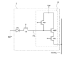
- FIG. 2 is an equivalent circuit diagram of a pixel of the photodetection device according to the first embodiment of the present technology.
- FIG. 2 is a longitudinal cross-sectional view showing a partial cross-sectional configuration of a first circuit configured on a first semiconductor substrate and a second circuit configured on a second semiconductor substrate in the photodetection device according to the first embodiment of the present technology.
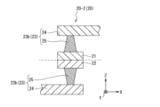
- FIG. 2 is a longitudinal cross-sectional view showing a part of the configuration of a connection line included in the photodetection device according to the first embodiment of the present technology.
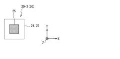
- FIG. 2 is a longitudinal cross-sectional view showing a part of the configuration of a connection line included in the photodetection device according to the first embodiment of the present technology.
- FIG. 2 is a longitudinal cross-sectional view showing a part of the configuration of a connection line included in the photodetection device according to the first embodiment of the present technology.
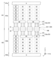
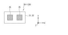
- 4A is a plan view showing the positional relationship between a connection pad and a vertical wiring portion in the connection line shown in FIG. 4A.
- FIG. FIG. 2 is a longitudinal cross-sectional view showing a part of the configuration of a connection line included in the photodetection device according to the first embodiment of the present technology.
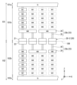
- FIG. 5A is a plan view showing the positional relationship between a connection pad and a vertical wiring portion in the connection line shown in FIG. 5A.
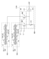
- FIG. FIG. 2 is an explanatory diagram showing a connection relationship between a detection circuit and a connection line included in the photodetection device according to the first embodiment of the present technology.
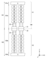
- FIG. 2 is a plan view schematically showing a planar arrangement of connection lines according to the first embodiment of the present technology.
- FIG. 7 is an explanatory diagram showing a connection relationship between a detection circuit and a connection line included in the photodetection device according to Modification 1 of the first embodiment of the present technology.
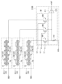
- FIG. 7 is an explanatory diagram showing a connection relationship between a detection circuit and a connection line included in a photodetection device according to a second modification of the first embodiment of the present technology.
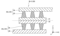
- FIG. 7 is a plan view showing the positional relationship between connection pads and vertical wiring portions in a third connection line according to Modification 2 of the first embodiment of the present technology. It is a longitudinal cross-sectional view which shows a part of other structure of the connection line of 3rd system
- 11A is a plan view showing the positional relationship between a connection pad and a vertical wiring portion in the connection line shown in FIG. 11A.
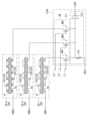
- FIG. 7 is an explanatory diagram showing a connection relationship between a detection circuit and a connection line included in a photodetection device according to a third modification of the first embodiment of the present technology.
- FIG. 7 is an explanatory diagram showing a connection relationship between a detection circuit and a connection line included in a photodetection device according to a second embodiment of the present technology.
- 14 is an explanatory diagram showing a specific configuration of the selector shown in FIG. 13.
- FIG. 15 is a diagram showing a truth table regarding input and output of the detection circuit shown in FIG. 14.
- FIG. FIG. 7 is an explanatory diagram showing a connection relationship between a detection circuit and a connection line included in a photodetection device according to Modification 1 of the second embodiment of the present technology.
- FIG. 17 is an explanatory diagram showing a specific configuration of the selector shown in FIG. 16.
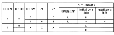
- FIG. 18 is a diagram showing a truth table regarding input and output of the detection circuit shown in FIG. 17.
- FIG. FIG. 1 is a block diagram showing an example of a schematic configuration of an electronic device.
- FIG. 1 is a block diagram showing an example of a schematic configuration of a vehicle control system.
- FIG. 2 is an explanatory diagram showing an example of installation positions of an outside-vehicle information detection section and an imaging section.
- CMOS Complementary Metal Oxide Semiconductor
- FIG. 1 is a block diagram illustrating a configuration example of a test system according to an embodiment of the present technology.
- This test system is for detecting the presence or absence of a failure in a semiconductor device such as a photodetector, and includes a photodetector 100 and a central processing unit or test device 300.
- the photodetector 100 also includes a pixel array section 110, a scan control section 120, a readout control section 130, a signal processing section 140, an output section 150, and a common control section 180.
- the photodetector 100 is mounted on the semiconductor chip 2.
- the semiconductor chip 2 includes a first semiconductor substrate 101 and a second semiconductor substrate 102 which are stacked and bonded to each other.
- the photodetection device 100 also includes a plurality of detection circuits 210 and a detection circuit control section 160 electrically connected to the plurality of detection circuits 210.
- the plurality of detection circuits 210 are respectively provided at different positions of the photodetection device 100 in plan view. Further, for each of the plurality of detection circuits 210, a plurality of connection lines, which will be described later, are provided.
- the detection circuit 210 only needs to be provided on one of the first semiconductor substrate 101 and the second semiconductor substrate 102 which are stacked and bonded, and does not need to be provided on both substrates. In this embodiment, the detection circuit 210 will be described as being provided on the second semiconductor substrate 102 of the first semiconductor substrate 101 and the second semiconductor substrate 102.
- the circuits within the photodetecting device 100 are distributed and arranged on the stacked first semiconductor substrate 101 and second semiconductor substrate 102.
- the pixel array section 110 is arranged on the first semiconductor substrate 101, and the remaining circuits are arranged on the second semiconductor substrate 102.
- the circuits arranged on each of the first semiconductor substrate 101 and the second semiconductor substrate 102 are not limited to the configuration illustrated in the figure.
- the pixel array section 110, the readout control section 130, and the comparator in the signal processing section 140 can be arranged on the first semiconductor substrate 101, and the remaining circuits can be arranged on the second semiconductor substrate 102.
- two semiconductor substrates (101 and 102) are stacked, it is also possible to stack three or more semiconductor substrates and arrange the circuits in the photodetecting device 100 on them.
- the pixel array section 110 At least a plurality of portions of the pixels 3 where photoelectric conversion is performed are arranged in a two-dimensional grid pattern.
- the pixel array section 110 is a light receiving surface that receives light collected by the optical system 402 shown in FIG. 19, for example.
- the scan control section 120 sequentially drives the rows of the pixel array section 110 under the control of the common control section 180 to output pixel signals.
- the readout control section 130 reads out pixel signals from each column of the pixel array section and supplies them to the signal processing section 140.
- the read control section 130 includes a read circuit 15.
- FIG. 2 is an equivalent circuit diagram showing an example of the configuration of the pixel 3.
- the pixel 3 includes a photoelectric conversion element PD, a charge accumulation region (floating diffusion) FD that accumulates (retains) signal charges photoelectrically converted by this photoelectric conversion element PD, and a charge accumulation region (floating diffusion) FD that accumulates (retains) signal charges photoelectrically converted by this photoelectric conversion element PD.
- a transfer transistor TR that transfers the signal charge to the charge storage region FD is provided.
- the pixel 3 includes a readout circuit 15 included in the readout control section 130. Readout circuit 15 is electrically connected to charge storage region FD.
- the photoelectric conversion element PD generates signal charges according to the amount of received light.
- the photoelectric conversion element PD also temporarily accumulates (retains) the generated signal charge.
- the photoelectric conversion element PD has a cathode side electrically connected to the source region of the transfer transistor TR, and an anode side electrically connected to a reference potential line (for example, ground).
- a photodiode is used as the photoelectric conversion element PD.
- the drain region of the transfer transistor TR is electrically connected to the charge storage region FD.
- a gate electrode of the transfer transistor TR is electrically connected to a transfer transistor drive line among the pixel drive lines.
- the charge accumulation region FD temporarily accumulates and holds signal charges transferred from the photoelectric conversion element PD via the transfer transistor TR.
- the readout circuit 15 reads out the signal charges accumulated in the charge accumulation region FD, and outputs a pixel signal based on the signal charges.
- the readout circuit 15 includes, for example, an amplification transistor AMP, a selection transistor SEL, and a reset transistor RST as pixel transistors, although they are not limited thereto.
- These transistors have, for example, a gate insulating film made of a silicon oxide film (SiO 2 film), a gate electrode, and a pair of main electrode regions that function as a source region and a drain region. It is composed of MOSFET.
- these transistors may be MISFETs (Metal Insulator Semiconductor FETs) in which the gate insulating film is a silicon nitride film (Si 3 N 4 film) or a laminated film such as a silicon nitride film and a silicon oxide film.
- MISFETs Metal Insulator Semiconductor FETs
- the gate insulating film is a silicon nitride film (Si 3 N 4 film) or a laminated film such as a silicon nitride film and a silicon oxide film.
- the amplification transistor AMP has a source region electrically connected to the drain region of the selection transistor SEL, and a drain region electrically connected to the power supply line Vdd and the drain region of the reset transistor.
- the gate electrode of the amplification transistor AMP is electrically connected to the charge storage region FD and the source region of the reset transistor RST.
- the selection transistor SEL has a source region electrically connected to the vertical signal line 11 (VSL), and a drain electrically connected to the source region of the amplification transistor AMP.
- the gate electrode of the selection transistor SEL is electrically connected to the selection transistor drive line among the pixel drive lines.
- the reset transistor RST has a source region electrically connected to the charge storage region FD and the gate electrode of the amplification transistor AMP, and a drain region electrically connected to the power supply line Vdd and the drain region of the amplification transistor AMP.
- a gate electrode of the reset transistor RST is electrically connected to a reset transistor drive line among the pixel drive lines.
- the signal processing unit 140 shown in FIG. 1 performs signal processing such as AD (Analog to Digital) conversion processing and CDS (Correlated Double Sampling) processing on pixel signals.
- the signal processing section 140 supplies the processed pixel signal to the output section 150.
- the output unit 150 outputs image data in which pixel signals are arranged to the central processing unit or the testing device 300.
- FIG. 3A is a vertical cross-sectional view showing a partial cross-sectional configuration of the first circuit C1 configured on the first semiconductor substrate 101 and the second circuit C2 configured on the second semiconductor substrate 102.
- first semiconductor substrate 101 and the second semiconductor substrate 102 are bonded together at the bonding surface 199.
- metal wiring layers are assumed as an example, and are indicated as M1 to M6 in order from the silicon (Si) layer.
- the first semiconductor substrate 101 has a semiconductor layer 101a and a wiring layer 101b stacked on the semiconductor layer 101a.
- a pixel array section 110, a photoelectric conversion element PD, etc. are configured in the semiconductor layer 101a.
- the wiring layer 101b includes an insulating film, a metal wiring layer, a connection pad 21 facing the bonding surface 199, and a via extending in the stacking direction and electrically connecting the connection pad 21 to the metal wiring layer M6 of the first circuit C1.
- This is a multilayer wiring layer having a certain vertical wiring portion 25.
- the second semiconductor substrate 102 includes a semiconductor layer 102a and a wiring layer 102b stacked on the semiconductor layer 102a. Elements such as transistors are configured in the semiconductor layer 102a.
- the wiring layer 102b includes an insulating film, a metal wiring layer, a connection pad 22 facing the bonding surface 199, and a via extending in the stacking direction and electrically connecting the connection pad 22 to the metal wiring layer M6 of the second circuit C2.
- This is a multilayer wiring layer having a certain vertical wiring portion 25.
- connection pad 21 and the connection pad 22 are hybrid-bonded. That is, the surface of the connection pad 21 facing the bonding surface 199 and the surface of the connection pad 22 facing the bonding surface 199 are overlapped and bonded. Then, by bonding the connection pads 21 and 22, the first circuit C1 mounted on the first semiconductor substrate 101 and the second circuit C2 mounted on the second semiconductor substrate 102 are electrically connected. are doing. Note that in order to distinguish between the connection pads 21 and 22 shown in FIG. 3A and the connection pads 21 and 22 shown in FIGS. 3B and 3C, which will be described later, the connection pads 21 and 22 shown in FIG. 22, and the test connection pads 21, 22 shown in FIGS. 3B and 3C may be blown.
- connection pads 21 and 22 are simply referred to as connection pads 21 and 22.
- the vertical wiring portion 25 shown in FIG. 3A is referred to as a circuit vertical wiring portion 25.
- the vertical wiring portion 25 shown in FIGS. 3B and 3C may be referred to as a test vertical wiring portion 25. Note that if the two are not distinguished, they are simply referred to as the vertical wiring portion 25.
- the circuit vertical wiring portion 25 is provided for each circuit connection pad.
- connection line 20 is a test pattern provided for detecting a failure in the bond between the first semiconductor substrate 101 and the second semiconductor substrate 102, and is provided for each detection circuit 210.
- the connection line 20 has a plurality of pairs of connection pads 21 and 22 connected to each other across the bonding surface 199 between the first semiconductor substrate 101 and the second semiconductor substrate 102, The first semiconductor substrate 101 and the second semiconductor substrate 102 are alternately routed a plurality of times from one to the other.
- the pair of connection pads 21 and 22 that the connection line 20 has is provided separately in addition to the connection pads (circuit connection pads) 21 and 22 that electrically connect the first circuit C1 and the second circuit C2 shown in FIG. 3A.
- connection pads 21 and 22 are made of metal.
- the connection pads 21 and 22 are made of, for example, but not limited to, copper (Cu). Note that the number of pairs of connection pads 21 and 22 that the connection line has is not limited to the number shown in FIGS. 3B, 3C, and the subsequent figures.
- the connection line 20 has a wiring member 23 that connects adjacent connection pads on each of the first semiconductor substrate 101 side and the second semiconductor substrate 102 side.
- the wiring member 23 has a horizontal wiring portion 24 extending in the horizontal direction, and a vertical wiring portion 25 extending in the stacking direction and connecting the connection pad 21 or the connection pad 22 to the horizontal wiring portion 24.
- the horizontal wiring portion 24 is, for example, a wiring belonging to the metal wiring layer M6, although it is not limited thereto.
- the vertical wiring portion 25 is, for example, a via, although it is not limited thereto.
- the horizontal wiring portion 24 and the vertical wiring portion 25 may be constructed using known metals.
- connection wire 20 is routed from the first semiconductor substrate 101 to the second semiconductor substrate 102 in the order of the wiring member 23, the connection pad 21, and the connection pad 22, and then the wiring member 23 and the connection pad 22 are routed in this order.
- the pad 22 and the connection pad 21 are routed from the second semiconductor substrate 102 to the first semiconductor substrate 101 in this order.
- the connection line 20 is alternately routed multiple times from one of the first semiconductor substrate 101 and the second semiconductor substrate 102 to the other.
- the connection wire 20 that connects a plurality of pairs of connection pads 21 and 22 in this way is called a daisy chain.
- failures that may occur in the bonding between the first semiconductor substrate 101 and the second semiconductor substrate 102 shown in FIG. 3A include, but are not limited to, failures related to the pair of connection pads 21 and 22, for example.
- Examples of failures related to the pair of connection pads 21 and 22 include poor bonding between the connection pads, peeling that occurs after bonding, and poor bonding due to misalignment during bonding of substrates.
- failures related to the pair of connection pads 21 and 22 include poor bonding and peeling between the connection pads 21 and 22 and the vertical wiring portion 25, which is a via, and wiring belonging to the vertical wiring portion 25 and the metal wiring layer M6.
- the above-described failure inspection is performed using the connection line 20 as a test pattern. If a failure similar to the above-described failure occurs in the connection line 20, the resistance value of the connection line 20 increases. Further, when a disconnection occurs in the connection line 20, electrical continuity of the connection line 20 is interrupted. Then, using the detection circuit 210, the presence or absence of a failure in the connection line 20 is inspected.
- the photodetection device 100 has multiple systems of connection lines 20 that are electrically isolated from each other.
- the photodetecting device 100 has two systems of connection lines 20, the connection line 20 shown in FIG. 3B and the connection line 20 shown in FIG. 3C.
- the connection line 20-2 is electrically separated from the connection line 20-1. Note that in order to distinguish between the connection line 20 shown in FIG. 3B and the connection line 20 shown in FIG. 3C, the connection line 20 shown in FIG. 3B is called a connection line 20-1, and the connection line 20 shown in FIG. It is called line 20-2. When the connection line 20-1 and the connection line 20-2 are not distinguished, they are simply referred to as the connection line 20 without being distinguished.
- Each of the plurality of connection lines 20 is inspected by the detection circuit 210 for the presence or absence of a failure. More specifically, one of the connection lines 20 of the plurality of systems is selected, and the selected connection line 20 is inspected for failure. In this embodiment, each of the connection line 20-1 and the connection line 20-2 is inspected by the detection circuit 210 for the presence or absence of a failure.
- each of the plurality of connection lines 20 has a different number of vertical wiring portions 25 provided for each connection pad.
- one connection line 20 can be said to be a connection line obtained by daisy-chaining a set of connection pads having the same number of vertical wiring portions 25.
- the photodetecting device 100 has a plurality of connection lines including a first connection line and a second connection line electrically separated from the first connection line as the connection line 20, and the first connection line is
- Each connection pad has M (M is an integer of 1 or more) vertical wiring portions 25, and the second connection line has N (N is an integer of 1 or more) vertical wiring portions 25 for each connection pad. , and M>N.
- M is an integer of 1 or more
- the wiring member 23a which is the wiring member included in the connection line 20-1, has one horizontal wiring portion 24 and two vertical wiring portions 25 provided for each connection pad.
- connection line 20-2 is a connection line obtained by daisy-chaining a plurality of sets of connection pads each having one vertical wiring portion 25 for each connection pad.
- the wiring member 23b which is the wiring member included in the connection line 20-2, has one horizontal wiring portion 24 and one vertical wiring portion 25 provided for each connection pad. Note that when the wiring member 23a and the wiring member 23b are not distinguished from each other, they are simply referred to as the wiring member 23.
- the number of vertical wiring portions 25 that the connection line 20-1 has for each connection pad is set to the same number as the number of circuit vertical wiring portions 25 provided for each of the circuit connection pads 21 and 22 shown in FIG. 3A (this embodiment In this case, it is set to 2).
- the number of vertical wiring portions 25 of the connection line 20-1 in this way, the presence or absence of a failure can be tested for the same configuration as the configuration for electrically connecting the first circuit C1 and the second circuit C2. be able to.
- the number of vertical wiring portions 25 that the connection line 20-2 has for each connection pad is smaller than the number of vertical wiring portions 25 that the connection line 20-1 has for each connection pad. In this embodiment, the number of vertical wiring portions 25 that the connection line 20-2 has for each connection pad is one.
- connection line 20-1 Since the connection line 20-1 has two vertical wiring portions 25 for each connection pad, for example, even if peeling occurs between the connection pad 21 and one vertical wiring portion 25, , there is a low possibility that the connection line 20-1 will be disconnected. That is, the connection line 20-1 has high robustness. On the other hand, since the connection line 20-2 has only one vertical wiring portion 25 for each connection pad, peeling occurs between the connection pad 21 and one vertical wiring portion 25. In this case, the possibility that the connection line 20-2 has a high resistance and is broken is higher than the possibility that the connection line 20-1 has a high resistance and a possibility that it is broken. In other words, the robustness of the connection line 20-2 is lower than that of the connection line 20-1, and it is more likely to fail than the connection line 20-1. Since the connection line 20-2 is more likely to fail than the connection line 20-2, it can be said that the test pattern for failure detection is a pattern with higher failure detection sensitivity than the connection line 20-1.
- connection line 20 is schematically drawn, and will also be schematically drawn in similar drawings hereinafter.
- the detection circuit 210 includes a failure detection circuit 211 and a selection circuit SW that selectively connects one connection line 20 of the plurality of connection lines 20 to the failure detection circuit 211.
- the configuration is such that the presence or absence of a failure is detected for the connection line 20 that has been damaged.
- two systems of connection lines 20, ie, connection line 20-1 and connection line 20-2, are selectively connected to failure detection circuit 211 by selection circuit SW. Therefore, the detection circuit 210 can directly detect the presence or absence of a failure in the connection line 20 connected to the failure detection circuit 211.
- the failure detection circuit 211 includes a resistance element 212 and a determination circuit 213.
- the first potential which is the potential at one end of the resistance element 212, is the reference potential VSS (eg, ground).
- the second potential which is the potential at one end of the connection line 20, is the power supply potential VDD, which is different from the first potential. In this embodiment, the second potential is higher than the first potential.
- the other end of the connection line 20 can be electrically connected to the other end of the resistance element 212 via the selection circuit SW.
- the selection circuit SW has a switch provided for each connection line 20.
- the selection circuit SW includes a switch SW1 provided between the connection line 20-1 and the resistance element 212 of the failure detection circuit 211, and a switch SW1 provided between the connection line 20-2 and the resistance element 212 of the failure detection circuit 211. and a switch SW2 provided between the two.
- the switches SW1 and SW2 are configured by, for example, but not limited to, pMOS transistors.
- the pMOS transistor turns on when "0" is input as the gate control signal SELSW to its gate electrode, electrically connects the connection line 20 to the resistance element 212 of the failure detection circuit 211, and outputs the gate control signal SELSW.
- connection line 20 When “1” is input as “1”, it is turned off and electrically disconnects between the connection line 20 and the resistance element 212 of the failure detection circuit 211.
- Each of the plurality of switches owned by the selection circuit SW is turned on and off under the control of the detection circuit control section 160. More specifically, by turning on only one of the plurality of switches under the control of the detection circuit control unit 160, the selection circuit SW selects one of the connection lines 20 of the plurality of connection lines 20. is selectively connected to the failure detection circuit 211.
- a drive line L1 is electrically connected to the gate electrode of the switch SW1, and a drive line L2 is electrically connected to the gate electrode of the switch SW2.
- the gate control signal SELSW is input to the gate electrode of the switch via the drive lines L1 and L2 under the control of the detection circuit control section 160. Furthermore, when no inspection is being performed, all the switches included in the selection circuit SW are turned off, thereby suppressing the flow of electricity to the connection line 20, thereby saving power consumption.
- the determination circuit 213 is a buffer connected between the connection line 20 connected to the failure detection circuit 211 and the resistance element 212.
- the determination circuit 213 detects a third potential that is a potential between the connection line 20 connected to the failure detection circuit 211 and the resistance element 212, and based on the third potential, determines whether the connection line 20 connected to the failure detection circuit 211 is connected to the failure detection circuit 211 or not. The presence or absence of a failure is detected for the connected connection line 20, and the result is output as an output signal OUT.
- the determination circuit 213 is, for example, a level shifter circuit, and compares the third potential with a failure threshold, and if the third potential is higher than the failure threshold, the connection line 20 connected to the failure detection circuit 211 is “H” indicating that there is no failure is output as the output signal OUT, and “L” indicating that there is a failure in the connection line 20 connected to the failure detection circuit 211 when the third potential is below the failure threshold. ” is output as the output signal OUT. If the connecting wire 20 connected to the failure detection circuit 211 has a failure such as peeling, it becomes difficult for electricity to flow through the connecting wire 20, and the resistance value of the connecting wire 20 increases. Then, the third potential becomes lower than when there is no failure.
- the third potential is lower than when there is no failure. Therefore, by comparing the third potential with the failure threshold, it is possible to detect whether or not there is a failure in the connection line 20 connected to the failure detection circuit 211.
- the value of the failure threshold can be changed by changing the resistance value of the resistance element 212.
- the resistance element 212 is, for example, a variable resistance as shown in the figure, although it is not limited thereto.
- FIG. 7 is a plan view schematically showing the planar arrangement of the connection lines 20-1 and 20-2.
- the connection lines 20-1 and 20-2 are routed while changing directions multiple times.
- the terminals that supply the power supply voltage VDD include a terminal that supplies voltage to the first circuit C1 and the second circuit C2, and a terminal that supplies voltage to the connection line 20.
- the connection lines 20-1 and 20-2 routed in this manner are provided for each of the detection circuits 210 shown in plurality in FIG. 1, and are arranged near the detection circuits 210.
- the common control unit 180 shown in FIG. 1 controls each of the circuits within the photodetector 100. Further, the common control unit 180 receives various instruction signals from the central processing unit or the testing device 300, and controls each of the circuits in the photodetection device 100 based on the received various instruction signals. For example, the common control unit 180 controls the operation timing of the scan control unit 120 and the signal processing unit 140 in synchronization with a vertical synchronization signal from the central processing unit or the testing device 300. Further, for example, the common control section 180 supplies a connection line selection signal received from the central processing section or the testing device 300 to the detection circuit control section 160. The connection line selection signal is a signal indicating which connection line among the plurality of connection lines 20 is to be inspected.
- the detection circuit control unit 160 is a circuit that controls the operation of the detection circuit 210 based on various instruction signals received from the common control unit 180. For example, the detection circuit control section 160 controls the selection circuit SW based on the connection line selection signal received from the common control section 180. Further, the detection circuit control unit 160 receives the output signal OUT from the detection circuit 210 and supplies the received output signal OUT or a signal indicating the output signal OUT to the central processing unit or the testing device 300.
- the central processing unit or test device 300 is, for example, an external device that tests the photodetector 100 for various failures.
- the central processing unit or the test device 300 uses, for example, the image data received from the photodetector 100 to detect the presence or absence of a failure in a circuit other than the detection circuit 210, such as a pixel in the pixel array unit 110. Further, the central processing unit or the test device 300 inspects the connection line 20, for example. In that case, the central processing unit or test device 300 supplies the connection line selection signal to the common control unit 180 and receives the output signal OUT or a signal indicating the output signal OUT from the detection circuit control unit 160.
- a detection circuit such as the detection circuit 210 and the detection circuit control section 160 are provided in the photodetection device 100, these circuits can also be provided in a semiconductor device other than the photodetection device 100.
- connection line 20 including the pair of connection pads 21 and 22 is directly connected to the connection line 20, and the presence or absence of a failure in the connection line 20 is detected. It has a detection circuit 210 that can perform direct detection. Therefore, a failure in the connection line 20 including the pair of connection pads 21 and 22 bonded to each other via the bonding surface 199 can be directly detected. Thereby, the accuracy of failure detection at the joint between the first semiconductor substrate 101 and the second semiconductor substrate 102 can be improved.
- the technology described in Patent Document 2 mentioned above is a technology that determines the presence or absence of a failure based on the response when charging and discharging, and it is difficult to optimize the failure detection circuit. Because of this, the test took time.
- the photodetection device 100 according to the first embodiment of the present technology has a simple configuration in which the third potential and the failure threshold are compared, and the result of comparing the third potential and the failure threshold is It outputs digitally in two values: “H” and “L”. Therefore, failure testing is easy, and since there is no need to use a time constant, it is possible to suppress an increase in the time required for testing.
- a failure detection circuit is provided for each chip of a plurality of chips that are bonded together.
- the photodetecting device 100 it is only necessary to provide the photodetector on one of the first semiconductor substrate 101 and the second semiconductor substrate 102 which are overlapped and bonded. . This can prevent the chip size from increasing.
- connection lines including a connection line 20-1 and a connection line 20-2 electrically separated from the connection line 20-1 are provided.
- the connection line 20-1 has M (M is an integer of 1 or more) vertical wiring portions 25 for each connection pad.
- the connection line 20-2 has N (N is an integer greater than or equal to 1) vertical wiring portions 25 for each connection pad, and M>N.
- connection line 20-1 has high robustness but low failure detection sensitivity as a test pattern compared to the connection line 20-2, and the connection line 20-1 has low robustness but has low failure detection sensitivity as a test pattern compared to the connection line 20-1. It has both connection lines with connection line 20-1, which has high failure detection sensitivity. Therefore, the failure state of the connection line 20 can be evaluated from multiple angles. For example, as a result of testing both the connection wire 20-1 and the connection wire 20-2, if no failure is detected in both, it is possible that the connection wire 20-1 is partially peeled off, etc. It can be seen that there is a low possibility that there is a serious failure.
- the detection circuit 210 selectively connects one of the connection lines 20 of the plurality of systems to the failure detection circuit 211. It has a selection circuit SW connected to the fault detection circuit 211, and is configured to detect the presence or absence of a fault in the connection line 20 connected to the fault detection circuit 211. In this way, by using the selection circuit SW, one detection circuit 210 can be shared by a plurality of connection lines 20, so that it is possible to suppress an increase in chip size.
- the number of vertical wiring portions 25 that the connection line 20-1 has for each connection pad is calculated from the number of vertical wiring portions 25 provided for each circuit connection pad.
- the number is the same as the number.
- the photodetection device 100 when no inspection is being performed, all the switches included in the selection circuit SW are turned off, thereby suppressing the flow of electricity to the connection line 20. , saving power consumption.
- the selection circuit SW is controlled based on the connection line selection signal from the central processing unit or the testing device 300, but the present technology is not limited to this.
- the detection circuit control unit 160 controls the selection circuit SW to sequentially test the plurality of connection lines 20 one by one. Also good.
- the number of circuit vertical wiring portions 25 provided for each circuit connection pad is two, but there is no limitation to this. Not done.
- the number of circuit vertical wiring portions 25 provided for each circuit connection pad may be one, or three or more. In the case of three or more, the number of vertical wiring portions 25 provided for each connection pad may be increased in accordance with the number of circuit vertical wiring portions 25 in the connection line 20-1 as well.
- one detection circuit 210 is shared by a plurality of connection lines 20, but a detection circuit 210 may be provided for each connection line.
- a photodetection device 100 according to Modification 1 of the first embodiment includes a detection circuit 210A instead of the detection circuit 210, as shown in FIG.
- the first potential which is the potential at one end of the resistance element 212 included in the detection circuit 210A, is the power supply potential VDD.
- the second potential which is the potential at one end of the connection line 20, is the reference potential VSS (eg, ground). That is, in this modification, the first potential is higher than the second potential.
- the switches SW1 and SW2 are configured with nMOS transistors.
- the nMOS transistor turns on when "1" is input as the gate control signal SELSW to its gate electrode, electrically connects the connection line 20 to the resistance element 212 of the failure detection circuit 211, and outputs the gate control signal SELSW.
- "0" is input as “0”, it is turned off and electrically disconnects between the connection line 20 and the resistance element 212 of the failure detection circuit 211.
- a photodetection device 100 according to a second modification of the first embodiment includes a detection circuit 210B instead of the detection circuit 210, as shown in FIG. Furthermore, the connection line 20 has three systems of connection lines: a connection line 20-1, a connection line 20-2, and a connection line 20-3. That is, the connection line 20-3 is the third system connection line. Then, the detection circuit 210B performs a failure test using the three connection lines 20 described above.
- the selection circuit SW of the detection circuit 210B includes a switch SW3 provided between the connection line 20-3 and the resistance element 212 of the failure detection circuit 211 in addition to the switches SW1 and SW2. In this way, the selection circuit SW has a configuration in which the number of switches corresponds to the number of connection lines 20.
- connection line 20-3 has four vertical wiring portions 25 for each connection pad.
- the wiring member 23c which is the wiring member included in the connection line 20-3, has one horizontal wiring portion 24 and four vertical wiring portions 25 provided for each connection pad.
- the positional relationship between the connection pads 21 and 22 of the connection line 20-3 and the vertical wiring portion 25 is, for example, as shown in FIG. 10, although it is not limited thereto.
- the cross-sectional structure of the connecting line 20-3 when viewed in longitudinal section is the same as that in FIG. 4A.
- connection line 20-3 The number of vertical wiring portions 25 that the connection line 20-3 has for each connection pad is greater than the number of circuit vertical wiring portions 25 provided for each circuit connection pad 21, 22 shown in FIG. 3A. With this configuration, the presence or absence of a failure can be inspected for the connection line 20-3, which has higher robustness than the configuration of the portion that electrically connects the first circuit C1 and the second circuit C2.
- the photodetection device 100 according to the second modification of the first embodiment has three systems of connection lines 20 with different robustness and failure detection sensitivity. Therefore, the failure state of the connection line 20 can be evaluated from more angles.
- connection line 20-3 which has a high robustness based on the configuration of the part that electrically connects the first circuit C1 and the second circuit C2.
- connection line 20-3 has a high robustness based on the configuration of the part that electrically connects the first circuit C1 and the second circuit C2.
- connection lines 20 Note that in this modification, three systems of connection lines 20 were provided, but four or more systems of connection lines 20 may be provided.
- the number of vertical wiring portions 25 that the connection line 20-3 has for each connection pad is four, but may be three as shown in FIGS. 11A and 11B. Furthermore, the number may be five or more.
- the number of circuit vertical wiring portions 25 provided for each circuit connection pad was two, but three. It may be more than one.
- the number of circuit vertical wiring portions 25 provided for each circuit connection pad is four, which is the same as in the case of connection line 20-3. That is, the connection line 20 having the same configuration as the configuration for electrically connecting the first circuit C1 and the second circuit C2 is the connection line 20-3.
- the configuration is such that a plurality of connection lines, more specifically connection lines 20-1 and 20-2, are provided as connection lines having lower robustness and higher failure detection sensitivity than the connection line 20-3.
- connection lines 20 as connection lines with lower robustness and higher failure detection sensitivity than the connection line 20-3, it is possible to determine, for example, what kind of failure will occur in the connection line 20. It is possible to obtain more knowledge such as from which part of 20 the failure occurs and how the failure progresses over time.
- the photodetection device 100 according to the third modification of the first embodiment includes a detection circuit 210C instead of the detection circuit 210, as shown in FIG. Further, the connection line 20 has a configuration in which the second potential, which is the potential at one end thereof, is different for each connection line of the plurality of connection lines 20.
- the second potential of the connection line 20-1 is the power supply potential VDD1
- the second potential of the connection line 20-2 is the power supply potential VDD2
- the second potential of the connection line 20-3 is the power supply potential VDD3.
- the power supply potentials VDD1, VDD2, and VDD3 are different potentials from each other.
- transistors having a breakdown voltage corresponding to the power supply potentials VDD1, VDD2, and VDD3 are provided as transistors forming the switches SW1, SW2, and SW3.
- the photodetection device 100 according to the second embodiment is different from the photodetection device 100 according to the first embodiment described above in that it has a detection circuit 210D instead of the detection circuit 210, and other photodetection devices.
- the configuration of the device 100 is basically the same as the photodetection device 100 of the first embodiment described above.
- the detection circuit 210D has a configuration that can be switched between an enable mode for testing whether there is a fault in the connection line 20 or a disable mode for testing for a fault in the detection circuit 210 itself. Note that the same reference numerals are given to the constituent elements that have already been explained, and the explanation thereof will be omitted.
- the connection line 20 is drawn more schematically than in other drawings.
- the inspection for various failures of the photodetector 100 performed by the central processing unit or the test device 300 shown in FIG. 1 includes inspection of the detection circuit 210 itself.
- the central processing unit or test device 300 supplies a mode signal to the common control unit 180.
- the mode signal is a signal indicating an instruction to switch the mode of the detection circuit 210D. More specifically, the mode signal is a signal indicating an instruction to switch the mode of the detection circuit 210D to one of the enable mode and the disable mode.
- the common control unit 180 supplies the mode signal from the central processing unit or the testing device 300 to the detection circuit control unit 160. Then, the detection circuit control section 160 controls the operation of the detection circuit 210 and the like based on the mode signal.
- connection line 20 has multiple systems of connection lines 20 from connection line 20-1 to connection line 20-n.
- the detection circuit 210D detects the presence or absence of a failure in the connection line 20 connected to the failure detection circuit 211 via the selection circuit SW.
- the selection circuit SW has switches from switch SW1 to switch SWn. Each switch of the selection circuit SW is constituted by a pMOS transistor. Further, the detection circuit 210D has drive lines L1 to Ln to which the gate control signal SELSW is input.
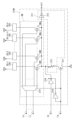
- the selection circuit SW has a selector 214. The selector 214 is electrically connected to the drive lines L1 to Ln, the gate electrode of each switch, and the drive line La described below.
- the determination circuit 213 included in the failure detection circuit 211 is an inverter circuit. Therefore, the determination circuit 213 outputs "L” as the output signal OUT when there is no failure in the connection line 20 connected to the failure detection circuit 211, and when there is no failure in the connection line 20 connected to the failure detection circuit 211. In some cases, "H” is output as the output signal OUT.
- the detection circuit 210D has a drive line La to which the control signal DETEN is input, and a drive line Lb to which the test signal TESTIN is input.
- the control signal DETEN and the test signal TESTIN are input to the drive lines La and Lb under the control of the detection circuit control section 160.
- the mode signal instructs to switch the mode of the detection circuit 210D to the enable mode "1" is input to the drive line La as the control signal DETEN.
- the mode signal instructs to switch the mode of the detection circuit 210D to the disable mode "0" is input to the drive line La as the control signal DETEN.
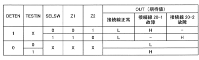
- FIG. 14 is a diagram showing the selector 214 when the connection line 20 has two systems, the connection line 20-1 and the connection line 20-2, and FIG. 15 shows the selector 214 when the connection line 20 has two systems. Represents a truth table. To simplify the explanation, the operation of the detection circuit 210D will be explained using an example in which there are two connection lines 20.
- the selector 214 has a NAND circuit for each switch.
- the output Z1 of the NAND circuit 215a is input to the gate electrode of the switch SW1, and the output Z2 of the NAND circuit 215b is input to the gate electrode of the switch SW2.
- “1” is input to both the NAND circuits 215a and 215b as the control signal DETEN.
- the gate control signal SELSW is input to the NAND circuit 215a via the inverter circuit 216, and the gate control signal SELSW is input as is to the NAND circuit 215b. That is, the configuration is such that one switch is selected from a plurality of switches depending on the presence or absence of the inverter circuit 216.
- the operation of the detection circuit 210D when the detection circuit 210D is switched to the disable mode will be described.
- the detection circuit 210D is switched to the disabled mode, it becomes possible to test whether the detection circuit 210 itself has a failure.
- "0" is input as the control signal DETEN to the drive line La
- the nMOS transistor 217 is turned off, and one end of the resistance element 212 and the reference potential VSS are electrically disconnected.
- the inverter circuit 218 included in the detection circuit 210D inverts the control signal DETEN to "1” and supplies this signal "1" to the inverter circuit 219.
- the inverter circuit 219 inverts the test signal TESTIN input to the drive line Lb, and the inverted test signal TESTIN is supplied to the determination circuit 213.
- the truth table in FIG. 15 shows the output signal OUT when there is no failure in the detection circuit 210D. If there is no failure in the detection circuit 210D, the output signal OUT becomes “L” when the test signal TESTIN is “0", and the output signal OUT becomes "H” when the test signal TESTIN is "1". On the other hand, although not shown, if there is a failure in the detection circuit 210D, the output signal OUT becomes "H” in response to "0" of the test signal TESTIN, and The output signal OUT becomes "L".
- the photodetecting device 100 includes a detection circuit 210E in place of the detection circuit 210D, as shown in FIGS. 16 to 18.
- the first potential which is the potential at one end of the resistance element 212 included in the detection circuit 210E, is the power supply potential VDD.
- the second potential which is the potential at one end of the connection line 20, is the reference potential VSS (eg, ground). That is, in this modification, the first potential is higher than the second potential. Because of this difference in configuration, the configuration of the detection circuit 210E of this modification differs in some parts from the configuration of the detection circuit 210D described in the second embodiment. The different parts will be explained below.
- each switch included in the selection circuit SW is configured with an nMOS transistor instead of a pMOS transistor.
- the detection circuit 210E includes a pMOS transistor 217 instead of the nMOS transistor 217, and the determination circuit 213 includes a buffer instead of the inverter circuit.
- the detection circuit 210E includes an inverter circuit 220. The input side of the inverter circuit 220 is connected to the drive line Lb, and the output side is connected to the input side of the inverter circuit 219. The inverter circuit 220 inverts the test signal TESTIN input via the drive line Lb. Then, the inverted test signal TESTIN is input to the inverter circuit 219.
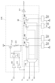
- FIG. 17 is a diagram showing the selector 214 when the connection lines 20 are two systems, the connection line 20-1 and the connection line 20-2.
- the selector 214 of this modification has an AND circuit 215c instead of the NAND circuit 215a, and an AND circuit 215d instead of the NAND circuit 215b.
- a control signal DETEN is input to both AND circuits 215c and 215d.
- the gate control signal SELSW is input to the AND circuit 215c via the inverter circuit 216, and the gate control signal SELSW is input as is to the AND circuit 215d.
- the configuration is such that one switch is selected from a plurality of switches depending on the presence or absence of the inverter circuit 216. Furthermore, the output Z1 of the AND circuit 215c is input to the gate electrode of the switch SW1, and the output Z2 of the AND circuit 215d is input to the gate electrode of the switch SW2.
- the gate control signal SELSW is input to the AND circuit 215c via the inverter circuit 216, and the gate control signal SELSW is input as is to the AND circuit 215d.
- the operation of the detection circuit 210E when the detection circuit 210E is switched to the disable mode will be described.
- the control signal DETEN is inverted by the inverter circuit 216, and the inverted control signal DETEN, that is, "1” is applied to the gate electrode of the pMOS transistor 217 of the detection circuit 210E.
- the pMOS transistor 217 is turned off. This electrically disconnects one end of resistance element 212 and power supply potential VDD.
- the test signal TESTIN input to the drive line Lb is inverted by the inverter circuit 220 and supplied to the inverter circuit 219.
- the other operations of the detection circuit 210E are the same as those of the detection circuit 210D, so the explanation thereof will be omitted here.
- the electronic device 400 includes a solid-state imaging device 401, an optical lens 402, a shutter device 403, a drive circuit 404, and a signal processing circuit 405.
- the electronic device 400 is, for example, an electronic device such as a camera, although it is not limited thereto. Further, the electronic device 400 includes the above-described photodetection device 100 as a solid-state imaging device 401.
- the optical lens (optical system) 402 forms an image of image light (incident light 406) from the subject onto the imaging surface of the solid-state imaging device 401.
- image light incident light 406
- the shutter device 403 controls the light irradiation period and the light blocking period to the solid-state imaging device 401.
- the drive circuit 404 supplies drive signals that control the transfer operation of the solid-state imaging device 401 and the shutter operation of the shutter device 403.
- Signal transfer of the solid-state imaging device 401 is performed by a drive signal (timing signal) supplied from the drive circuit 404 .
- the signal processing circuit 405 performs various signal processing on the signals (pixel signals) output from the solid-state imaging device 401.
- the video signal subjected to signal processing is stored in a storage medium such as a memory, or output to a monitor.
- the electronic device 400 is not limited to a camera, and may be another electronic device.
- it may be an imaging device such as a camera module for mobile devices such as mobile phones.
- the electronic device 400 also includes, as the solid-state imaging device 401, the photodetecting device 100 according to any one of the first embodiment to the second embodiment and modifications of these embodiments, or the first embodiment to the second embodiment.
- a photodetecting device 100 according to a combination of at least two of the embodiments and modifications of these embodiments can be provided.
- the technology according to the present disclosure (this technology) can be applied to various products.
- the technology according to the present disclosure may be realized as a device mounted on any type of moving body such as a car, electric vehicle, hybrid electric vehicle, motorcycle, bicycle, personal mobility, airplane, drone, ship, robot, etc. It's okay.
- FIG. 20 is a block diagram illustrating a schematic configuration example of a vehicle control system, which is an example of a mobile body control system to which the technology according to the present disclosure can be applied.
- the vehicle control system 12000 includes a plurality of electronic control units connected via a communication network 12001.
- the vehicle control system 12000 includes a drive system control unit 12010, a body system control unit 12020, an outside vehicle information detection unit 12030, an inside vehicle information detection unit 12040, and an integrated control unit 12050.
- a microcomputer 12051, an audio/image output section 12052, and an in-vehicle network I/F (interface) 12053 are illustrated.
- the drive system control unit 12010 controls the operation of devices related to the drive system of the vehicle according to various programs.
- the drive system control unit 12010 includes a drive force generation device such as an internal combustion engine or a drive motor that generates drive force for the vehicle, a drive force transmission mechanism that transmits the drive force to wheels, and a drive force transmission mechanism that controls the steering angle of the vehicle. It functions as a control device for a steering mechanism to adjust and a braking device to generate braking force for the vehicle.
- the body system control unit 12020 controls the operations of various devices installed in the vehicle body according to various programs.
- the body system control unit 12020 functions as a keyless entry system, a smart key system, a power window device, or a control device for various lamps such as a headlamp, a back lamp, a brake lamp, a turn signal, or a fog lamp.
- radio waves transmitted from a portable device that replaces a key or signals from various switches may be input to the body control unit 12020.
- the body system control unit 12020 receives input of these radio waves or signals, and controls the door lock device, power window device, lamp, etc. of the vehicle.
- the external information detection unit 12030 detects information external to the vehicle in which the vehicle control system 12000 is mounted.
- an imaging section 12031 is connected to the outside-vehicle information detection unit 12030.
- the vehicle exterior information detection unit 12030 causes the imaging unit 12031 to capture an image of the exterior of the vehicle, and receives the captured image.
- the external information detection unit 12030 may perform object detection processing such as a person, car, obstacle, sign, or text on the road surface or distance detection processing based on the received image.
- the imaging unit 12031 is an optical sensor that receives light and outputs an electrical signal according to the amount of received light.
- the imaging unit 12031 can output the electrical signal as an image or as distance measurement information.
- the light received by the imaging unit 12031 may be visible light or non-visible light such as infrared rays.
- the in-vehicle information detection unit 12040 detects in-vehicle information.
- a driver condition detection section 12041 that detects the condition of the driver is connected to the in-vehicle information detection unit 12040.
- the driver condition detection unit 12041 includes, for example, a camera that images the driver, and the in-vehicle information detection unit 12040 detects the degree of fatigue or concentration of the driver based on the detection information input from the driver condition detection unit 12041. It may be calculated, or it may be determined whether the driver is falling asleep.
- the microcomputer 12051 calculates control target values for the driving force generation device, steering mechanism, or braking device based on the information inside and outside the vehicle acquired by the vehicle exterior information detection unit 12030 or the vehicle interior information detection unit 12040, Control commands can be output to 12010.
- the microcomputer 12051 realizes ADAS (Advanced Driver Assistance System) functions, including vehicle collision avoidance or impact mitigation, following distance based on vehicle distance, vehicle speed maintenance, vehicle collision warning, vehicle lane departure warning, etc. It is possible to perform cooperative control for the purpose of ADAS (Advanced Driver Assistance System) functions, including vehicle collision avoidance or impact mitigation, following distance based on vehicle distance, vehicle speed maintenance, vehicle collision warning, vehicle lane departure warning, etc. It is possible to perform cooperative control for the purpose of
- ADAS Advanced Driver Assistance System
- the microcomputer 12051 controls the driving force generating device, steering mechanism, braking device, etc. based on information about the surroundings of the vehicle acquired by the vehicle exterior information detection unit 12030 or the vehicle interior information detection unit 12040. It is possible to perform cooperative control for the purpose of autonomous driving, etc., which does not rely on operation.
- the microcomputer 12051 can output a control command to the body system control unit 12020 based on the information outside the vehicle acquired by the outside information detection unit 12030.
- the microcomputer 12051 controls the headlamps according to the position of the preceding vehicle or oncoming vehicle detected by the vehicle exterior information detection unit 12030, and performs cooperative control for the purpose of preventing glare, such as switching from high beam to low beam. It can be carried out.
- the audio and image output unit 12052 transmits an output signal of at least one of audio and images to an output device that can visually or audibly notify information to the occupants of the vehicle or to the outside of the vehicle.
- an audio speaker 12061, a display section 12062, and an instrument panel 12063 are illustrated as output devices.
- the display unit 12062 may include, for example, at least one of an on-board display and a head-up display.
- FIG. 21 is a diagram showing an example of the installation position of the imaging section 12031.
- the vehicle 12100 has imaging units 12101, 12102, 12103, 12104, and 12105 as the imaging unit 12031.
- the imaging units 12101, 12102, 12103, 12104, and 12105 are provided, for example, at positions such as the front nose, side mirrors, rear bumper, back door, and the top of the windshield inside the vehicle 12100.
- An imaging unit 12101 provided in the front nose and an imaging unit 12105 provided above the windshield inside the vehicle mainly acquire images in front of the vehicle 12100.
- Imaging units 12102 and 12103 provided in the side mirrors mainly capture images of the sides of the vehicle 12100.
- An imaging unit 12104 provided in the rear bumper or back door mainly captures images of the rear of the vehicle 12100.
- the images of the front acquired by the imaging units 12101 and 12105 are mainly used for detecting preceding vehicles, pedestrians, obstacles, traffic lights, traffic signs, lanes, and the like.
- FIG. 21 shows an example of the imaging range of the imaging units 12101 to 12104.
- An imaging range 12111 indicates the imaging range of the imaging unit 12101 provided on the front nose
- imaging ranges 12112 and 12113 indicate imaging ranges of the imaging units 12102 and 12103 provided on the side mirrors, respectively
- an imaging range 12114 shows the imaging range of the imaging unit 12101 provided on the front nose.
- the imaging range of the imaging unit 12104 provided in the rear bumper or back door is shown. For example, by overlapping the image data captured by the imaging units 12101 to 12104, an overhead image of the vehicle 12100 viewed from above can be obtained.
- At least one of the imaging units 12101 to 12104 may have a function of acquiring distance information.
- at least one of the imaging units 12101 to 12104 may be a stereo camera including a plurality of image sensors, or may be an image sensor having pixels for phase difference detection.
- the microcomputer 12051 determines the distance to each three-dimensional object within the imaging ranges 12111 to 12114 and the temporal change in this distance (relative speed with respect to the vehicle 12100) based on the distance information obtained from the imaging units 12101 to 12104. In particular, by determining the three-dimensional object that is closest to the vehicle 12100 on its path and that is traveling at a predetermined speed (for example, 0 km/h or more) in approximately the same direction as the vehicle 12100, it is possible to extract the three-dimensional object as the preceding vehicle. can.
- a predetermined speed for example, 0 km/h or more
- the microcomputer 12051 can set an inter-vehicle distance to be secured in advance in front of the preceding vehicle, and perform automatic brake control (including follow-up stop control), automatic acceleration control (including follow-up start control), and the like. In this way, it is possible to perform cooperative control for the purpose of autonomous driving, etc., in which the vehicle travels autonomously without depending on the driver's operation.
- the microcomputer 12051 transfers three-dimensional object data to other three-dimensional objects such as two-wheeled vehicles, regular vehicles, large vehicles, pedestrians, and utility poles based on the distance information obtained from the imaging units 12101 to 12104. It can be classified and extracted and used for automatic obstacle avoidance. For example, the microcomputer 12051 identifies obstacles around the vehicle 12100 into obstacles that are visible to the driver of the vehicle 12100 and obstacles that are difficult to see. Then, the microcomputer 12051 determines a collision risk indicating the degree of risk of collision with each obstacle, and when the collision risk exceeds a set value and there is a possibility of a collision, the microcomputer 12051 transmits information via the audio speaker 12061 and the display unit 12062. By outputting a warning to the driver via the vehicle control unit 12010 and performing forced deceleration and avoidance steering via the drive system control unit 12010, driving support for collision avoidance can be provided.
- the microcomputer 12051 determines a collision risk indicating the degree of risk of collision with each obstacle, and when the collision risk exceed
- At least one of the imaging units 12101 to 12104 may be an infrared camera that detects infrared rays.
- the microcomputer 12051 can recognize a pedestrian by determining whether the pedestrian is present in the images captured by the imaging units 12101 to 12104.
- pedestrian recognition involves, for example, a procedure for extracting feature points in images captured by the imaging units 12101 to 12104 as infrared cameras, and a pattern matching process is performed on a series of feature points indicating the outline of an object to determine whether it is a pedestrian or not.
- the audio image output unit 12052 creates a rectangular outline for emphasis on the recognized pedestrian.
- the display unit 12062 is controlled to display the .
- the audio image output unit 12052 may control the display unit 12062 to display an icon or the like indicating a pedestrian at a desired position.
- the technology according to the present disclosure can be applied to, for example, the imaging unit 12031 among the configurations described above.
- the above-described photodetection device 100 can be applied to the imaging section 12031.
- the present technology can be applied to all light detection devices, including not only the solid-state imaging device as an image sensor described above, but also a ranging sensor that measures distance, also called a ToF (Time of Flight) sensor.
- a distance measurement sensor emits illumination light toward an object, detects the reflected light that is reflected back from the object's surface, and measures the flight from the time the illumination light is emitted until the reflected light is received. This is a sensor that calculates the distance to an object based on time.
- the structure of this distance measurement sensor the structure of the connection line and detection circuit described above can be adopted.
- the present technology is also applicable to semiconductor devices other than the photodetecting device 100.
- semiconductor devices such as memories such as DRAMs, logic circuits, or combinations thereof.
- the materials listed as constituting the above-mentioned constituent elements may contain additives, impurities, and the like.
- the present technology may have the following configuration. (1) a first semiconductor substrate; a second semiconductor substrate superposed and bonded to the first semiconductor substrate; The first semiconductor substrate and the second semiconductor substrate have a plurality of pairs of connection pads connected to each other across a bonding surface between the first semiconductor substrate and the second semiconductor substrate, and the first semiconductor substrate and the second semiconductor substrate are connected to each other through the pairs of connection pads.
- connection line alternately routed multiple times from one side of the semiconductor substrate to the other, a detection circuit capable of detecting the presence or absence of a failure in the connection line; Equipped with The connection line has a wiring member that connects the adjacent connection pads on each of the first semiconductor substrate side and the second semiconductor substrate side, The wiring member has a horizontal wiring portion extending in the horizontal direction and a vertical wiring portion extending in the stacking direction and connecting the connection pad to the horizontal wiring portion,
- the connection line includes a plurality of connection lines including a first connection line and a second connection line electrically separated from the first connection line,
- the first connection line has M (M is an integer of 1 or more) the vertical wiring portions for each connection pad, and the second connection line has N (N is an integer of 1 or more) for each of the connection pads.
- the detection circuit includes a failure detection circuit and a selection circuit that selectively connects one of the connection lines of the plurality of systems to the failure detection circuit, and is connected to the failure detection circuit.
- the failure detection circuit includes a resistance element and a determination circuit,
- the potential at one end of the resistive element is a first potential
- the potential at one end of the connection line is a second potential different from the first potential
- the other end of the connection line is electrically connectable to the other end of the resistance element via the selection circuit
- the determination circuit is capable of detecting a third potential that is a potential at a position between the connection line connected to the failure detection circuit and the resistance element, and based on the third potential, the determination circuit detects the failure detection circuit.
- the determination circuit is a level shifter circuit that determines whether the third potential is greater than a failure threshold.
- a first circuit configured on the first semiconductor substrate; a second circuit configured on the second semiconductor substrate; a pair of circuit connection pads, which are connection pads provided separately in addition to the connection pads of the connection line; a circuit vertical wiring portion provided for each circuit connection pad and extending in the stacking direction; In the first semiconductor substrate, the first circuit and the circuit connection pad are electrically connected by the circuit vertical wiring portion, In the second semiconductor substrate, the second circuit and the circuit connection pad are electrically connected by the circuit vertical wiring portion, (1) to (4), wherein the first connection line has the same number of vertical wiring portions for each connection pad as the number of circuit vertical wiring portions provided for each circuit connection pad; The semiconductor device according to any one of the above.
- (10) comprising: a semiconductor device that is a photodetection device; and an optical system that forms image light from a subject on the semiconductor device;
- the semiconductor device includes: a first semiconductor substrate; a second semiconductor substrate superposed and bonded to the first semiconductor substrate;
- the first semiconductor substrate and the second semiconductor substrate have a plurality of pairs of connection pads connected to each other across a bonding surface between the first semiconductor substrate and the second semiconductor substrate, and the first semiconductor substrate and the second semiconductor substrate are connected to each other via the pairs of connection pads.
- connection line alternately routed multiple times from one side of the semiconductor substrate to the other, a detection circuit capable of detecting the presence or absence of a failure in the connection line; Equipped with The connection line has a wiring member that connects the adjacent connection pads on each of the first semiconductor substrate side and the second semiconductor substrate side, The wiring member has a horizontal wiring portion extending in the horizontal direction and a vertical wiring portion extending in the stacking direction and connecting the connection pad to the horizontal wiring portion,
- the connection line includes a plurality of connection lines including a first connection line and a second connection line electrically separated from the first connection line,
- the first connection line has M (M is an integer of 1 or more) the vertical wiring portions for each connection pad, and the second connection line has N (N is an integer of 1 or more) for each of the connection pads.
Landscapes
- Engineering & Computer Science (AREA)
- Physics & Mathematics (AREA)
- General Physics & Mathematics (AREA)
- Computer Hardware Design (AREA)
- Microelectronics & Electronic Packaging (AREA)
- General Engineering & Computer Science (AREA)
- Environmental & Geological Engineering (AREA)
- Multimedia (AREA)
- Signal Processing (AREA)
- Health & Medical Sciences (AREA)
- Toxicology (AREA)
- Testing Or Measuring Of Semiconductors Or The Like (AREA)
- Tests Of Electronic Circuits (AREA)
- Solid State Image Pick-Up Elements (AREA)
- Semiconductor Integrated Circuits (AREA)
- Testing Of Short-Circuits, Discontinuities, Leakage, Or Incorrect Line Connections (AREA)
Abstract
Description
1.第1実施形態
2.第2実施形態
3.応用例
電子機器への応用例
移動体への応用例
この実施形態では、裏面照射型のCMOS(Complementary Metal Oxide Semiconductor)イメージセンサである光検出装置に本技術を適用した一例について説明する。なお、光検出装置は、半導体装置の一例である。
図1は、本技術の実施形態におけるテストシステムの一構成例を示すブロック図である。このテストシステムは、光検出装置などの半導体装置の故障の有無を検出するためのものであり、光検出装置100と、中央演算部または試験装置300とを備える。また、光検出装置100は、画素アレイ部110、走査制御部120、読出し制御部130、信号処理部140、出力部150および共通制御部180を備える。
光検出装置100は、半導体チップ2に搭載されている。半導体チップ2は、互いに重ね合わせて接合された第1半導体基板101と、第2半導体基板102とを有する。また、光検出装置100は、複数の検出回路210と、複数の検出回路210に電気的に接続された検出回路制御部160とを備える。複数の検出回路210は、それぞれ平面視で光検出装置100の異なる位置に設けられている。また、複数の検出回路210のそれぞれに対して、後述の複数系統の接続線が設けられている。なお、検出回路210は、重ね合わせて接合された第1半導体基板101と、第2半導体基板102との一方の基板に設けられていればよく、両方の基板に設ける必要はない。本実施形態では、検出回路210は、第1半導体基板101と第2半導体基板102とのうちの第2半導体基板102に設けられているとして、説明する。
図1に示すように、中央演算部または試験装置300は、例えば、光検出装置100の各種故障の検査を行う外部装置である。中央演算部または試験装置300は、例えば、光検出装置100から受け取った画像データを用いて、画素アレイ部110内の画素など、検出回路210以外の回路の故障の有無を検出する。また、中央演算部または試験装置300は、例えば、接続線20の検査を行う。その場合、中央演算部または試験装置300は、接続線選択信号を共通制御部180に供給し、検出回路制御部160から、出力信号OUT、又は出力信号OUTを示す信号を受け取る。
以下、第1実施形態の主な効果を説明するが、その前に、従来の技術について、説明する。上述の特許文献1及び特許文献2に記載の技術は、半導体基板同士を貼り合わせることにより互いに接合される接続パッドの対に関する故障を、直接検出していなかった。特許文献1では、クラックテスト配線をTSV近傍に配置し、その配線の断線の有無を検出することにより、TSV近傍にクラックが生じているかどうかを検出するテストを行っていた。また、特許文献2では、TSVを大きい容量と捉えて、検査を行っていた。そのため、特許文献2の技術を、接続パッドに適用することができなかった。
以下、第1実施形態の変形例について、説明する。
第1実施形態の変形例1に係る光検出装置100では、図8に示すように、検出回路210に代えて検出回路210Aを有している。検出回路210Aが有する抵抗素子212の一端の電位である第1電位は、電源電位VDDである。そして、接続線20の一端の電位である第2電位が基準電位VSS(例えば、グラウンド)である。すなわち、本変形例では、第1電位は第2電位より高い構成である。また、本変形例では、スイッチSW1、SW2が、nMOSトランジスタにより構成されている。nMOSトランジスタは、そのゲート電極に、ゲート制御信号SELSWとして“1”が入力された場合にオンして、接続線20を故障検出回路211の抵抗素子212に電気的に接続し、ゲート制御信号SELSWとして“0”が入力された場合にオフして、接続線20と故障検出回路211の抵抗素子212との間を電気的に遮断する。
第1実施形態の変形例2に係る光検出装置100は、図9に示すように、検出回路210に代えて検出回路210Bを有している。また、接続線20は、接続線20-1と、接続線20-2と、接続線20-3との3系統の接続線を有する構成である。すなわち、接続線20-3が3系統目の接続線である。そして、検出回路210Bは、上述の3系統の接続線20を用いて、故障の検査を行っている。
第1実施形態の変形例3に係る光検出装置100は、図12に示すように、検出回路210に代えて検出回路210Cを有している。また、接続線20は、その一端の電位である第2電位が、複数系統の接続線20の各接続線において異なる構成である。
図13から図15までに示す本技術の第2実施形態について、以下に説明する。本第2実施形態に係る光検出装置100が上述の第1実施形態に係る光検出装置100と相違するのは、検出回路210に代えて検出回路210Dを有する点であり、それ以外の光検出装置100の構成は、基本的に上述の第1実施形態の光検出装置100と基本的には同様の構成になっている。検出回路210Dは、接続線20に故障があるか否かを検査するイネーブルモード及び検出回路210自体に故障があるか否かを検査するディセーブルモードの一方のモードに切り替え可能な構成を有する。なお、すでに説明した構成要素については、同じ符号を付してその説明を省略する。また、図13においては、他の図面と比べて接続線20をより模式的に描いている。
この第2実施形態の係る光検出装置100であっても、上述の第1実施形態に係る光検出装置100と同様の効果が得られる。
以下、第2実施形態の変形例について、説明する。
第2実施形態の変形例1に係る光検出装置100では、図16から図18までに示すように、検出回路210Dに代えて検出回路210Eを有している。検出回路210Eが有する抵抗素子212の一端の電位である第1電位は、電源電位VDDである。そして、接続線20の一端の電位である第2電位が基準電位VSS(例えば、グラウンド)である。すなわち、本変形例では、第1電位は第2電位より高い構成である。このような構成の違いがあるので、本変形例の検出回路210Eの構成は、第2実施形態で説明した検出回路210Dの構成と異なる部分がある。以下、異なる部分について、説明する。
<1.電子機器への応用例>
次に、図19に示す本技術の応用例に係る電子機器400について説明する。電子機器400は、固体撮像装置401と、光学レンズ402と、シャッタ装置403と、駆動回路404と、信号処理回路405とを備えている。電子機器400は、これに限定されないが、例えば、カメラ等の電子機器である。また、電子機器400は、固体撮像装置401として、上述の光検出装置100を備えている。
本開示に係る技術(本技術)は、様々な製品へ応用することができる。例えば、本開示に係る技術は、自動車、電気自動車、ハイブリッド電気自動車、自動二輪車、自転車、パーソナルモビリティ、飛行機、ドローン、船舶、ロボット等のいずれかの種類の移動体に搭載される装置として実現されてもよい。
上記のように、本技術は第1実施形態から第2実施形態までによって記載したが、この開示の一部をなす論述及び図面は本技術を限定するものであると理解すべきではない。この開示から当業者には様々な代替の実施形態、実施例及び運用技術が明らかとなろう。
(1)
第1半導体基板と、
前記第1半導体基板に重ね合わされて接合された第2半導体基板と、
前記第1半導体基板と前記第2半導体基板との接合面を挟んで互いに接続された接続パッドの対を複数対有し、前記接続パッドの前記対を介して前記第1半導体基板及び前記第2半導体基板のうちの一方から他方へと交互に複数回引き回された接続線と、
前記接続線の故障の有無を検出可能な検出回路と、
を備え、
前記接続線は、前記第1半導体基板側及び前記第2半導体基板側のそれぞれにおいて、隣接する前記接続パッド同士を接続する配線部材を有し、
前記配線部材は、水平方向に延びた水平配線部分と、積層方向に延び且つ前記接続パッドを前記水平配線部分に接続する垂直配線部分とを有し、
前記接続線としては、第1接続線と、前記第1接続線とは電気的に分離された第2接続線とを含む複数系統の接続線を有し、
前記第1接続線は前記接続パッド毎にM(Mは1以上の整数)個の前記垂直配線部分を有し、前記第2接続線は前記接続パッド毎にN(Nは1以上の整数)個の前記垂直配線部分を有し、且つM>Nである、
半導体装置。
(2)
前記検出回路は、故障検出回路と、前記複数系統の前記接続線のうちの一の接続線を前記故障検出回路に選択的に接続する選択回路とを有し、前記故障検出回路に接続された前記接続線について、故障の有無を検出可能である、(1)に記載の半導体装置。
(3)
前記故障検出回路は、抵抗素子と、判定回路とを有し、
前記抵抗素子の一端の電位は第1電位であり、
前記接続線の一端の電位は前記第1電位とは異なる第2電位であり、
前記接続線の他端は、前記選択回路を介して前記抵抗素子の他端に電気的に接続可能であり、
前記判定回路は、前記故障検出回路に接続された前記接続線と前記抵抗素子との間の位置の電位である第3電位を検出可能であり、前記第3電位に基づいて、前記故障検出回路に接続された前記接続線について故障の有無を検出可能である、(2)に記載の半導体装置。
(4)
前記判定回路は、前記第3電位が故障閾値より大きいか否かを判定するレベルシフタ回路である、(3)に記載の半導体装置。
(5)
前記第1半導体基板に構成された第1回路と、
前記第2半導体基板に構成された第2回路と、
前記接続線が有する前記接続パッド以外に別途設けられた前記接続パッドである回路接続パッドの対と、
前記回路接続パッド毎に設けられ且つ積層方向に延びた回路垂直配線部分と、を有し、
前記第1半導体基板において、前記第1回路と前記回路接続パッドとの間は前記回路垂直配線部分により電気的に接続されていて、
前記第2半導体基板において、前記第2回路と前記回路接続パッドとの間は前記回路垂直配線部分により電気的に接続されていて、
前記第1接続線が前記接続パッド毎に有する前記垂直配線部分の個数を、前記回路接続パッド毎に設けられた前記回路垂直配線部分の個数と同じに設けている、(1)から(4)のいずれかに記載の半導体装置。
(6)
N=1である、(1)から(5)のいずれかに記載の半導体装置。
(7)
3系統以上の前記接続線を有し、
前記接続パッド毎に設けられた前記垂直配線部分の個数は、前記複数系統の前記接続線毎に異なる、(1)から(6)のいずれかに記載の半導体装置。
(8)
前記接続線の一端の電位である前記第2電位は、前記複数系統の前記接続線毎に異なる、(3)又は(4)に記載の半導体装置。
(9)
前記第1半導体基板及び前記第2半導体基板の一方の基板が有する半導体層には、光電変換素子が構成されている、(1)から(8)のいずれかに記載の半導体装置。
(10)
光検出装置である半導体装置と、前記半導体装置に被写体からの像光を結像させる光学系と、を備え、
前記半導体装置は、
第1半導体基板と、
前記第1半導体基板に重ね合わされて接合された第2半導体基板と、
前記第1半導体基板と前記第2半導体基板との接合面を挟んで互いに接続された接続パッドの対を複数対有し、前記接続パッドの前記対を介して前記第1半導体基板及び前記第2半導体基板のうちの一方から他方へと交互に複数回引き回された接続線と、
前記接続線の故障の有無を検出可能な検出回路と、
を備え、
前記接続線は、前記第1半導体基板側及び前記第2半導体基板側のそれぞれにおいて、隣接する前記接続パッド同士を接続する配線部材を有し、
前記配線部材は、水平方向に延びた水平配線部分と、積層方向に延び且つ前記接続パッドを前記水平配線部分に接続する垂直配線部分とを有し、
前記接続線としては、第1接続線と、前記第1接続線とは電気的に分離された第2接続線とを含む複数系統の接続線を有し、
前記第1接続線は前記接続パッド毎にM(Mは1以上の整数)個の前記垂直配線部分を有し、前記第2接続線は前記接続パッド毎にN(Nは1以上の整数)個の前記垂直配線部分を有し、且つM>Nである、
電子機器。
3 画素
20、20-1、20-2、20-3 接続線
21、22 接続パッド
21、22 回路接続パッド
21、22 テスト接続パッド
23、23a、23b、23c 配線部材
24 水平配線部分
25 垂直配線部分
25 回路垂直配線部分
25 テスト垂直配線部分
100 光検出装置
101 第1半導体基板
102 第2半導体基板
110 画素アレイ部
120 走査制御部
130 制御部
140 信号処理部
150 出力部
160 検出回路制御部
180 共通制御部
199 接合面
210、210A、210B、210C、210D、210E 検出回路
211 故障検出回路
212 抵抗素子
213 判定回路
214 セレクタ
300 試験装置
C1 第1回路
C2 第2回路
DETEN 制御信号
OUT 出力信号
SELSW ゲート制御信号
SW 選択回路
SW1、SW2、SW3、 スイッチ
Claims (10)
- 第1半導体基板と、
前記第1半導体基板に重ね合わされて接合された第2半導体基板と、
前記第1半導体基板と前記第2半導体基板との接合面を挟んで互いに接続された接続パッドの対を複数対有し、前記接続パッドの前記対を介して前記第1半導体基板及び前記第2半導体基板のうちの一方から他方へと交互に複数回引き回された接続線と、
前記接続線の故障の有無を検出可能な検出回路と、
を備え、
前記接続線は、前記第1半導体基板側及び前記第2半導体基板側のそれぞれにおいて、隣接する前記接続パッド同士を接続する配線部材を有し、
前記配線部材は、水平方向に延びた水平配線部分と、積層方向に延び且つ前記接続パッドを前記水平配線部分に接続する垂直配線部分とを有し、
前記接続線としては、第1接続線と、前記第1接続線とは電気的に分離された第2接続線とを含む複数系統の接続線を有し、
前記第1接続線は前記接続パッド毎にM(Mは1以上の整数)個の前記垂直配線部分を有し、前記第2接続線は前記接続パッド毎にN(Nは1以上の整数)個の前記垂直配線部分を有し、且つM>Nである、
半導体装置。 - 前記検出回路は、故障検出回路と、前記複数系統の前記接続線のうちの一の接続線を前記故障検出回路に選択的に接続する選択回路とを有し、前記故障検出回路に接続された前記接続線について、故障の有無を検出可能である、請求項1に記載の半導体装置。
- 前記故障検出回路は、抵抗素子と、判定回路とを有し、
前記抵抗素子の一端の電位は第1電位であり、
前記接続線の一端の電位は前記第1電位とは異なる第2電位であり、
前記接続線の他端は、前記選択回路を介して前記抵抗素子の他端に電気的に接続可能であり、
前記判定回路は、前記故障検出回路に接続された前記接続線と前記抵抗素子との間の位置の電位である第3電位を検出可能であり、前記第3電位に基づいて、前記故障検出回路に接続された前記接続線について故障の有無を検出可能である、請求項2に記載の半導体装置。 - 前記判定回路は、前記第3電位が故障閾値より大きいか否かを判定するレベルシフタ回路である、請求項3に記載の半導体装置。
- 前記第1半導体基板に構成された第1回路と、
前記第2半導体基板に構成された第2回路と、
前記接続線が有する前記接続パッド以外に別途設けられた前記接続パッドである回路接続パッドの対と、
前記回路接続パッド毎に設けられ且つ積層方向に延びた回路垂直配線部分と、を有し、
前記第1半導体基板において、前記第1回路と前記回路接続パッドとの間は前記回路垂直配線部分により電気的に接続されていて、
前記第2半導体基板において、前記第2回路と前記回路接続パッドとの間は前記回路垂直配線部分により電気的に接続されていて、
前記第1接続線が前記接続パッド毎に有する前記垂直配線部分の個数を、前記回路接続パッド毎に設けられた前記回路垂直配線部分の個数と同じに設けている、請求項1に記載の半導体装置。 - N=1である、請求項1に記載の半導体装置。
- 3系統以上の前記接続線を有し、
前記接続パッド毎に設けられた前記垂直配線部分の個数は、前記複数系統の前記接続線毎に異なる、請求項1に記載の半導体装置。 - 前記接続線の一端の電位である前記第2電位は、前記複数系統の前記接続線毎に異なる、請求項3に記載の半導体装置。
- 前記第1半導体基板及び前記第2半導体基板の一方の基板が有する半導体層には、光電変換素子が構成されている、請求項1に記載の半導体装置。
- 光検出装置である半導体装置と、前記半導体装置に被写体からの像光を結像させる光学系と、を備え、
前記半導体装置は、
第1半導体基板と、
前記第1半導体基板に重ね合わされて接合された第2半導体基板と、
前記第1半導体基板と前記第2半導体基板との接合面を挟んで互いに接続された接続パッドの対を複数対有し、前記接続パッドの前記対を介して前記第1半導体基板及び前記第2半導体基板のうちの一方から他方へと交互に複数回引き回された接続線と、
前記接続線の故障の有無を検出可能な検出回路と、
を備え、
前記接続線は、前記第1半導体基板側及び前記第2半導体基板側のそれぞれにおいて、隣接する前記接続パッド同士を接続する配線部材を有し、
前記配線部材は、水平方向に延びた水平配線部分と、積層方向に延び且つ前記接続パッドを前記水平配線部分に接続する垂直配線部分とを有し、
前記接続線としては、第1接続線と、前記第1接続線とは電気的に分離された第2接続線とを含む複数系統の接続線を有し、
前記第1接続線は前記接続パッド毎にM(Mは1以上の整数)個の前記垂直配線部分を有し、前記第2接続線は前記接続パッド毎にN(Nは1以上の整数)個の前記垂直配線部分を有し、且つM>Nである、
電子機器。
Priority Applications (4)
| Application Number | Priority Date | Filing Date | Title |
|---|---|---|---|
| US18/845,174 US20250180635A1 (en) | 2022-04-26 | 2023-04-10 | Semiconductor device and electronic apparatus |
| CN202380035115.1A CN119072776A (zh) | 2022-04-26 | 2023-04-10 | 半导体装置及电子设备 |
| KR1020247038110A KR20250007556A (ko) | 2022-04-26 | 2023-04-10 | 반도체 장치 및 전자 기기 |
| DE112023002031.0T DE112023002031T5 (de) | 2022-04-26 | 2023-04-10 | Halbleitervorrichtung und elektronische Vorrichtung |
Applications Claiming Priority (2)
| Application Number | Priority Date | Filing Date | Title |
|---|---|---|---|
| JP2022072195 | 2022-04-26 | ||
| JP2022-072195 | 2022-04-26 |
Publications (1)
| Publication Number | Publication Date |
|---|---|
| WO2023210329A1 true WO2023210329A1 (ja) | 2023-11-02 |
Family
ID=88518388
Family Applications (1)
| Application Number | Title | Priority Date | Filing Date |
|---|---|---|---|
| PCT/JP2023/014587 Ceased WO2023210329A1 (ja) | 2022-04-26 | 2023-04-10 | 半導体装置及び電子機器 |
Country Status (5)
| Country | Link |
|---|---|
| US (1) | US20250180635A1 (ja) |
| KR (1) | KR20250007556A (ja) |
| CN (1) | CN119072776A (ja) |
| DE (1) | DE112023002031T5 (ja) |
| WO (1) | WO2023210329A1 (ja) |
Citations (2)
| Publication number | Priority date | Publication date | Assignee | Title |
|---|---|---|---|---|
| WO2021171785A1 (ja) * | 2020-02-28 | 2021-09-02 | ソニーセミコンダクタソリューションズ株式会社 | 半導体装置、および、テストシステム |
| JP2022050238A (ja) * | 2020-09-17 | 2022-03-30 | キオクシア株式会社 | 半導体装置 |
Family Cites Families (6)
| Publication number | Priority date | Publication date | Assignee | Title |
|---|---|---|---|---|
| US7605476B2 (en) * | 2005-09-27 | 2009-10-20 | Stmicroelectronics S.R.L. | Stacked die semiconductor package |
| KR101212777B1 (ko) | 2011-04-27 | 2012-12-14 | 에스케이하이닉스 주식회사 | 반도체 집적회로의 테스트 회로 및 방법 |
| US9128123B2 (en) * | 2011-06-03 | 2015-09-08 | Taiwan Semiconductor Manufacturing Company, Ltd. | Interposer test structures and methods |
| JP6054029B2 (ja) | 2011-12-22 | 2016-12-27 | ピーエスフォー ルクスコ エスエイアールエルPS4 Luxco S.a.r.l. | 半導体チップおよび半導体装置 |
| KR101353322B1 (ko) | 2012-05-24 | 2014-01-17 | 이승범 | 탄두의 탄대부 제청기와 분진흡수장치 |
| US10262911B1 (en) * | 2016-12-14 | 2019-04-16 | Xilinx, Inc. | Circuit for and method of testing bond connections between a first die and a second die |
-
2023
- 2023-04-10 KR KR1020247038110A patent/KR20250007556A/ko active Pending
- 2023-04-10 US US18/845,174 patent/US20250180635A1/en active Pending
- 2023-04-10 WO PCT/JP2023/014587 patent/WO2023210329A1/ja not_active Ceased
- 2023-04-10 DE DE112023002031.0T patent/DE112023002031T5/de active Pending
- 2023-04-10 CN CN202380035115.1A patent/CN119072776A/zh active Pending
Patent Citations (2)
| Publication number | Priority date | Publication date | Assignee | Title |
|---|---|---|---|---|
| WO2021171785A1 (ja) * | 2020-02-28 | 2021-09-02 | ソニーセミコンダクタソリューションズ株式会社 | 半導体装置、および、テストシステム |
| JP2022050238A (ja) * | 2020-09-17 | 2022-03-30 | キオクシア株式会社 | 半導体装置 |
Also Published As
| Publication number | Publication date |
|---|---|
| US20250180635A1 (en) | 2025-06-05 |
| KR20250007556A (ko) | 2025-01-14 |
| DE112023002031T5 (de) | 2025-02-20 |
| CN119072776A (zh) | 2024-12-03 |
Similar Documents
| Publication | Publication Date | Title |
|---|---|---|
| KR102246424B1 (ko) | 촬상 장치 및 촬상 방법, 카메라 모듈, 및 전자 기기 | |
| US12349487B2 (en) | Solid-state image pickup device and electronic apparatus | |
| JP7854129B2 (ja) | 固体撮像装置、および、撮像システム | |
| US20230062826A1 (en) | Solid-state imaging device and imaging device with combined dynamic vision sensor and imaging functions | |
| WO2022196141A1 (ja) | 固体撮像装置および電子機器 | |
| US12323722B2 (en) | Imaging device and electronic apparatus | |
| US20250201639A1 (en) | Semiconductor device, manufacturing method thereof, and electronic apparatus | |
| CN111886855B (zh) | 摄像装置和电子设备 | |
| TWI868130B (zh) | 成像裝置 | |
| US12165615B2 (en) | Imaging devices and imaging apparatuses, and methods for the same | |
| WO2024084865A1 (ja) | 半導体装置 | |
| US20250180635A1 (en) | Semiconductor device and electronic apparatus | |
| US11917312B2 (en) | Solid-state imaging apparatus | |
| US20250227390A1 (en) | Linear sensor | |
| WO2023090053A1 (ja) | 光検出装置及び電子機器 | |
| WO2025062845A1 (ja) | 光検出装置、電子機器及び光検出装置の製造方法 | |
| WO2026105480A1 (ja) | 光検出装置 | |
| WO2023013178A1 (ja) | 固体撮像装置及び電子機器 | |
| WO2025239294A1 (ja) | 半導体装置及び光検出装置 | |
| WO2024135493A1 (ja) | 光検出装置 | |
| CN118284973A (zh) | 光电转换元件和摄像装置 | |
| WO2025239288A1 (ja) | 光検出装置 | |
| WO2024038757A1 (ja) | 半導体装置および電子機器 | |
| WO2022181161A1 (ja) | 固体撮像装置及びその製造方法 | |
| WO2024241891A1 (ja) | 固体撮像装置および電子機器 |
Legal Events
| Date | Code | Title | Description |
|---|---|---|---|
| 121 | Ep: the epo has been informed by wipo that ep was designated in this application |
Ref document number: 23796074 Country of ref document: EP Kind code of ref document: A1 |
|
| WWE | Wipo information: entry into national phase |
Ref document number: 18845174 Country of ref document: US |
|
| WWE | Wipo information: entry into national phase |
Ref document number: 202380035115.1 Country of ref document: CN |
|
| ENP | Entry into the national phase |
Ref document number: 20247038110 Country of ref document: KR Kind code of ref document: A |
|
| WWE | Wipo information: entry into national phase |
Ref document number: 1020247038110 Country of ref document: KR |
|
| WWE | Wipo information: entry into national phase |
Ref document number: 112023002031 Country of ref document: DE |
|
| WWP | Wipo information: published in national office |
Ref document number: 112023002031 Country of ref document: DE |
|
| 122 | Ep: pct application non-entry in european phase |
Ref document number: 23796074 Country of ref document: EP Kind code of ref document: A1 |
|
| WWP | Wipo information: published in national office |
Ref document number: 18845174 Country of ref document: US |
|
| NENP | Non-entry into the national phase |
Ref country code: JP |