WO2023209986A1 - 薄型配線部材の製造方法、薄型配線部材、及び、配線基板の製造方法 - Google Patents
薄型配線部材の製造方法、薄型配線部材、及び、配線基板の製造方法 Download PDFInfo
- Publication number
- WO2023209986A1 WO2023209986A1 PCT/JP2022/019395 JP2022019395W WO2023209986A1 WO 2023209986 A1 WO2023209986 A1 WO 2023209986A1 JP 2022019395 W JP2022019395 W JP 2022019395W WO 2023209986 A1 WO2023209986 A1 WO 2023209986A1
- Authority
- WO
- WIPO (PCT)
- Prior art keywords
- wiring
- layer
- manufacturing
- thin
- support layer
- Prior art date
- Legal status (The legal status is an assumption and is not a legal conclusion. Google has not performed a legal analysis and makes no representation as to the accuracy of the status listed.)
- Ceased
Links
Images





Classifications
-
- H—ELECTRICITY
- H05—ELECTRIC TECHNIQUES NOT OTHERWISE PROVIDED FOR
- H05K—PRINTED CIRCUITS; CASINGS OR CONSTRUCTIONAL DETAILS OF ELECTRIC APPARATUS; MANUFACTURE OF ASSEMBLAGES OF ELECTRICAL COMPONENTS
- H05K3/00—Apparatus or processes for manufacturing printed circuits
- H05K3/007—Manufacture or processing of a substrate for a printed circuit board supported by a temporary or sacrificial carrier
-
- H—ELECTRICITY
- H10—SEMICONDUCTOR DEVICES; ELECTRIC SOLID-STATE DEVICES NOT OTHERWISE PROVIDED FOR
- H10W—GENERIC PACKAGES, INTERCONNECTIONS, CONNECTORS OR OTHER CONSTRUCTIONAL DETAILS OF DEVICES COVERED BY CLASS H10
- H10W90/00—Package configurations
- H10W90/401—Package configurations characterised by multiple insulating or insulated package substrates, interposers or RDLs
-
- H—ELECTRICITY
- H05—ELECTRIC TECHNIQUES NOT OTHERWISE PROVIDED FOR
- H05K—PRINTED CIRCUITS; CASINGS OR CONSTRUCTIONAL DETAILS OF ELECTRIC APPARATUS; MANUFACTURE OF ASSEMBLAGES OF ELECTRICAL COMPONENTS
- H05K1/00—Printed circuits
- H05K1/02—Details
- H05K1/03—Use of materials for the substrate
- H05K1/0313—Organic insulating material
-
- H—ELECTRICITY
- H05—ELECTRIC TECHNIQUES NOT OTHERWISE PROVIDED FOR
- H05K—PRINTED CIRCUITS; CASINGS OR CONSTRUCTIONAL DETAILS OF ELECTRIC APPARATUS; MANUFACTURE OF ASSEMBLAGES OF ELECTRICAL COMPONENTS
- H05K3/00—Apparatus or processes for manufacturing printed circuits
- H05K3/0011—Working of insulating substrates or insulating layers
- H05K3/0044—Mechanical working of the substrate, e.g. drilling or punching
- H05K3/0052—Depaneling, i.e. dividing a panel into circuit boards; Working of the edges of circuit boards
-
- H—ELECTRICITY
- H05—ELECTRIC TECHNIQUES NOT OTHERWISE PROVIDED FOR
- H05K—PRINTED CIRCUITS; CASINGS OR CONSTRUCTIONAL DETAILS OF ELECTRIC APPARATUS; MANUFACTURE OF ASSEMBLAGES OF ELECTRICAL COMPONENTS
- H05K3/00—Apparatus or processes for manufacturing printed circuits
- H05K3/22—Secondary treatment of printed circuits
- H05K3/28—Applying non-metallic protective coatings
- H05K3/281—Applying non-metallic protective coatings by means of a preformed insulating foil
-
- H—ELECTRICITY
- H05—ELECTRIC TECHNIQUES NOT OTHERWISE PROVIDED FOR
- H05K—PRINTED CIRCUITS; CASINGS OR CONSTRUCTIONAL DETAILS OF ELECTRIC APPARATUS; MANUFACTURE OF ASSEMBLAGES OF ELECTRICAL COMPONENTS
- H05K3/00—Apparatus or processes for manufacturing printed circuits
- H05K3/46—Manufacturing multilayer circuits
-
- H—ELECTRICITY
- H05—ELECTRIC TECHNIQUES NOT OTHERWISE PROVIDED FOR
- H05K—PRINTED CIRCUITS; CASINGS OR CONSTRUCTIONAL DETAILS OF ELECTRIC APPARATUS; MANUFACTURE OF ASSEMBLAGES OF ELECTRICAL COMPONENTS
- H05K3/00—Apparatus or processes for manufacturing printed circuits
- H05K3/46—Manufacturing multilayer circuits
- H05K3/4611—Manufacturing multilayer circuits by laminating two or more circuit boards
- H05K3/4626—Manufacturing multilayer circuits by laminating two or more circuit boards characterised by the insulating layers or materials
-
- H—ELECTRICITY
- H10—SEMICONDUCTOR DEVICES; ELECTRIC SOLID-STATE DEVICES NOT OTHERWISE PROVIDED FOR
- H10W—GENERIC PACKAGES, INTERCONNECTIONS, CONNECTORS OR OTHER CONSTRUCTIONAL DETAILS OF DEVICES COVERED BY CLASS H10
- H10W70/00—Package substrates; Interposers; Redistribution layers [RDL]
- H10W70/01—Manufacture or treatment
- H10W70/05—Manufacture or treatment of insulating or insulated package substrates, or of interposers, or of redistribution layers
-
- H—ELECTRICITY
- H10—SEMICONDUCTOR DEVICES; ELECTRIC SOLID-STATE DEVICES NOT OTHERWISE PROVIDED FOR
- H10W—GENERIC PACKAGES, INTERCONNECTIONS, CONNECTORS OR OTHER CONSTRUCTIONAL DETAILS OF DEVICES COVERED BY CLASS H10
- H10W70/00—Package substrates; Interposers; Redistribution layers [RDL]
- H10W70/60—Insulating or insulated package substrates; Interposers; Redistribution layers
- H10W70/62—Insulating or insulated package substrates; Interposers; Redistribution layers characterised by their interconnections
- H10W70/65—Shapes or dispositions of interconnections
-
- H—ELECTRICITY
- H10—SEMICONDUCTOR DEVICES; ELECTRIC SOLID-STATE DEVICES NOT OTHERWISE PROVIDED FOR
- H10W—GENERIC PACKAGES, INTERCONNECTIONS, CONNECTORS OR OTHER CONSTRUCTIONAL DETAILS OF DEVICES COVERED BY CLASS H10
- H10W70/00—Package substrates; Interposers; Redistribution layers [RDL]
- H10W70/60—Insulating or insulated package substrates; Interposers; Redistribution layers
- H10W70/67—Insulating or insulated package substrates; Interposers; Redistribution layers characterised by their insulating layers or insulating parts
- H10W70/68—Shapes or dispositions thereof
- H10W70/685—Shapes or dispositions thereof comprising multiple insulating layers
Definitions
- the present disclosure relates to a method for manufacturing a thin wiring member, a thin wiring member, and a method for manufacturing a wiring board.
- Patent Document 1 discloses an example of a fan-out type semiconductor device.
- a rewiring layer is provided between the semiconductor chip and the external connection terminal, and the rewiring layer widens the interval between the terminals of the semiconductor chip and connects the semiconductor chip to the external connection terminal.
- a rewiring layer is sometimes formed on a substrate, but it is sometimes difficult to miniaturize the rewiring layer due to reasons such as large variations in the height of the substrate. Therefore, a method is being considered in which a rewiring layer consisting of fine wiring is created by patterning on a flat glass carrier and then transferred.
- the rewiring layer is a thin member with a thickness of, for example, 50 ⁇ m, has adhesiveness and elasticity, and has an unstable shape, making it difficult to handle during transfer. More specifically, when a large number of redistribution layers are fabricated on a glass carrier all at once, it is necessary to separate them into individual redistribution layers, but it is difficult to dice them with precision. .
- An object of the present disclosure is to provide a method for manufacturing a thin wiring member, a thin wiring member, and a method for manufacturing a wiring board, which can accurately separate thin wiring members with unstable shapes into individual pieces. do.
- This manufacturing method is a method of manufacturing a plurality of thin wiring members, and includes a step of preparing a first carrier, a plurality of wiring parts corresponding to the plurality of thin wiring members, and insulation existing around the plurality of wiring parts. forming a support layer harder than the insulating part of the wiring layer on the first carrier; forming a support layer having at least one of the plurality of wiring parts; The method includes a step of separating a wiring body including a wiring layer and a support layer into pieces.
- a support layer is formed which is harder than the insulating part of the wiring layer, and the wiring includes the wiring layer and the support layer so that each wiring part has at least one wiring part among the plurality of wiring parts. It separates the body into pieces.
- the wiring layer having an unstable shape can be separated into pieces while the hard support layer supports the wiring layer. Therefore, according to this manufacturing method, it is possible to accurately separate a thin wiring member having an unstable shape into individual pieces.
- the wiring layer may peel up due to impact during singulation (for example, dicing), but with this manufacturing method, the support layer supports the wiring layer. , it is possible to suppress such turning up.
- the wiring body in the step of singulating, may be singulated with the support layer stuck to one surface of the wiring layer.
- the wiring body in the step of dividing into pieces, may be diced with a blade from the support layer toward the wiring layer to be divided into pieces.
- the wiring layer since dicing is performed from the hard support layer side, the wiring layer, which is cut after the support layer and whose shape is unstable, can be diced with precision by the blade, and it is possible to improve dicing performance. .
- the wiring body in the step of dividing into pieces, may be diced into pieces with the wiring layer sandwiched between the first carrier and the support layer. In this case, dicing is performed with the wiring layer whose shape is unstable being sandwiched between the first carrier and the hard support layer and its movement is fixed, making it possible to perform dicing with higher precision.
- the method for manufacturing the above-mentioned thin wiring member includes a step of pasting the singulated wiring body on an adhesive film, a step of removing the first carrier from the wiring body after being pasted on the adhesive film, and a step of attaching the singulated wiring body to the adhesive film.
- the method may further include the step of dividing the adhesive film to which the body is attached.
- the dividing method for example, a method of burning out with a laser, a method of dividing with a blade, a method of dividing by expanding, etc. can be applied.
- the adhesive film in the pasting step, the adhesive film may be pasted on the support layer of the wiring body, and in the dividing step, the adhesive film may be divided along the cutting region of the support layer.
- the support layer in the step of forming the support layer, the support layer may be formed on the first carrier, and in the step of forming the wiring layer, the wiring layer may be formed on the support layer.
- the hard support layer makes it possible to more reliably fix the wiring layer, which is unstable in shape, and to separate it into pieces. Therefore, according to this manufacturing method, it is possible to singulate pieces with high precision.
- the wiring body in the step of separating into pieces, may be diced with a blade from the wiring layer toward the support layer to be separated into pieces.
- the wiring layer is diced, since the wiring layer is firmly supported by the hard support layer on the opposite side, the wiring layer can be diced with the wiring layer fixed to some extent. Therefore, according to this manufacturing method, it is possible to accurately dice a thin wiring member having an unstable shape.
- the wiring layer is thin, it is expected that the wiring layer will roll up due to the water pressure during dicing, but by providing a support layer under the wiring layer, it is possible to suppress this rolling up. becomes.
- the method for manufacturing the thin wiring member described above includes the steps of attaching a second carrier to the surface of the wiring layer opposite to the surface to which the support layer is attached, and after attaching the second carrier,
- the method may include a step of removing the carrier, and a step of attaching the wiring body to which the second carrier is attached to an adhesive film.
- the step of singulating after being attached to the adhesive film, the wiring layer, the support layer, and the adhesive film may be diced and separated into pieces.
- the first carrier to which the support layer is attached can be removed, the support layer can be removed by etching or the like.
- the adhesive film is also diced, there is no need for expansion, and when the adhesive film is expanded, it is possible to prevent deterioration in the dimensional accuracy of the wiring layer due to division of the adhesive film.
- the method for manufacturing a thin wiring member described above further includes a step of removing the second carrier, and in the step of separating into pieces, after removing the second carrier, the wiring layer, the support layer, and the adhesive film are diced and separated. It may be fragmented.
- the material of the second carrier can be selected more freely.
- the dicing speed can be increased, and the manufacturing efficiency can be improved.
- the second carrier, the wiring layer, the support layer, and the adhesive film may be diced into pieces.
- dicing is performed with the wiring layer whose shape is unstable being sandwiched between the second carrier and the hard support layer and its movement is fixed, making it possible to perform dicing with high precision.
- the thickness of the wiring layer may be 200 ⁇ m or less. In this case, the thickness of the thin wiring member can be reduced more reliably. Moreover, even if the thickness of the wiring layer is 200 ⁇ m or less, according to any of the above-mentioned manufacturing methods, it is possible to precisely separate a wiring body having a wiring layer whose shape is unstable.
- the thickness of the support layer may be 25% or more and 3000% or less of the thickness of the wiring layer.
- the thickness of the support layer is 25% or more of the thickness of the wiring layer, it becomes possible to firmly support the wiring layer whose shape is unstable with the support layer and to accurately separate the wiring layer into pieces. Further, since the thickness of the support layer is 3000% or less of the thickness of the wiring layer, the thickness of the thin wiring member can be kept thin without increasing the thickness.
- the support layer may be formed of a material with a bending modulus of 3 GPa or more (or a bending strength of 700 MPa or more).
- the hard support layer can reliably support the wiring layer whose shape is unstable. Therefore, according to this manufacturing method, it is possible to separate into pieces with high precision.
- the support layer may include a thermosetting resin layer containing an inorganic filler.
- the inorganic filler allows the blade to exhibit a self-sharpening effect.
- the content of the inorganic filler in the thermosetting resin layer is preferably 40% by mass or more and 90% by mass or less. This makes it possible to achieve both supportability and cuttability of the wiring layer.
- the average particle size of the inorganic filler is preferably 0.05 ⁇ m or more, more preferably 0.1 ⁇ m or more.
- the first carrier may be a glass carrier having an arithmetic mean roughness of 50 nm or less. In this case, it becomes possible to accurately miniaturize the wiring layer formed on the first carrier.
- the wiring layer may include wiring with a line width of 5 ⁇ m or less. In this case, a thin wiring member having fine wiring can be obtained.
- the present disclosure relates to a thin wiring member.
- This thin wiring member includes wiring and a wiring layer having a resin composition or a cured product thereof existing around the wiring, and a support layer provided on one surface of the wiring layer.
- the support layer is made of a material harder than the resin composition of the wiring layer or its cured product.
- This thin wiring member has a support layer made of a material harder than the resin composition of the wiring layer or its cured product. In this case, when manufacturing a wiring board or a semiconductor device using the thin wiring member, it is possible to prevent the thin wiring member from warping or curling, and the shape can be stabilized.
- the thickness of the wiring layer is 200 ⁇ m or less
- the thickness of the support layer is 50 ⁇ m or more and 1200 ⁇ m or less
- the wiring layer may have wiring with a line width of 5 ⁇ m. In this case, a thin wiring member having fine wiring can be obtained.
- the support layer may be formed of a material with a bending modulus of 3 GPa or more (or a bending strength of 700 MPa or more). In this case, it is possible to more reliably prevent the thin wiring member from warping or curling, and the shape can be stabilized.
- the support layer may include a thermosetting resin layer containing an inorganic filler.
- the content of the inorganic filler in the thermosetting resin layer may be 40% by mass or more and 90% by mass or less. In this case, it becomes possible to achieve both supportability and cuttability of the wiring layer.
- the present disclosure relates to a method for manufacturing a wiring board.
- This wiring board manufacturing method includes a step of preparing a thin wiring member manufactured by any of the above-mentioned thin wiring member manufacturing methods, a step of arranging the thin wiring member on or in the board, and a step of preparing the thin wiring member. and a step of connecting the wiring to the connection terminal.
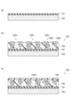
- FIG. 1 is a sectional view showing an example of a thin wiring member.
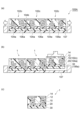
- FIGS. 2A to 2C are diagrams sequentially showing a method for manufacturing the thin wiring member shown in FIG. 1.
- FIGS. 3A to 3C are views sequentially showing a method for manufacturing the thin wiring member shown in FIG. 1, and show steps performed subsequent to the step shown in FIG. 2.
- FIGS. 4A to 4C are views sequentially showing a method for manufacturing the thin wiring member shown in FIG. 1, and show steps performed subsequent to the step shown in FIG. 3.
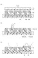
- FIGS. 5A to 5C are diagrams sequentially showing a method of manufacturing a wiring board using a thin wiring member.
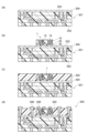
- FIGS. 6(a) to 6(c) are views sequentially showing another method of manufacturing the thin wiring member shown in FIG. 1.
- FIGS. 7A to 7C are views sequentially showing another method of manufacturing the thin wiring member shown in FIG. 1, and show steps performed subsequent to the step shown in FIG. 6.
- FIGS. 8(a) to 8(c) are views sequentially showing another method of manufacturing the thin wiring member shown in FIG. 1, and show steps performed subsequent to the step shown in FIG. 7.
- FIGS. 9(a) to 9(c) are views sequentially showing still another method of manufacturing the thin wiring member shown in FIG. 1, and show steps performed subsequent to the step shown in FIG. 7.
- FIGS. 10A to 10D are diagrams sequentially showing another method of manufacturing a wiring board using a thin wiring member.
- the term “layer” includes not only a structure formed on the entire surface but also a structure formed on a part of the layer when observed in a plan view.
- the term “process” is included in the present term not only when it refers to an independent process but also when it cannot be clearly distinguished from other processes, as long as the intended purpose of the process is achieved.
- a numerical range indicated using “ ⁇ ” indicates a range that includes the numerical values written before and after " ⁇ " as the minimum and maximum values, respectively. Further, in the numerical ranges described stepwise in this specification, the upper limit or lower limit of the numerical range of one step may be replaced with the upper limit or lower limit of the numerical range of another step.
- FIG. 1 is a sectional view showing an example of a thin wiring member.
- the thin wiring member 1 is a member used, for example, to configure a rewiring layer (RDL) of a wiring portion of a wiring board 200, which will be described later (see FIG. 5).
- RDL rewiring layer
- the thin wiring member 1 may be used for wiring or connection in a semiconductor device or the like.
- the thin wiring member 1 includes a fine wiring layer 10, a support layer 20, and an adhesive layer 30.
- the thin wiring member 1 is a minute wiring member that can be built into various wiring boards, semiconductor devices, etc., and may have, for example, a rectangular shape of 50 mm in height x 50 mm in width when viewed from above, or 20 mm in height x 50 mm in width. It may have a rectangular shape with a width of 20 mm. Further, the thin wiring member 1 is a thin wiring member, has a fine wiring layer 10 having a thickness of about 50 ⁇ m, and has a thin overall thickness of, for example, 30 ⁇ m to 1 mm. Note that the thickness of the fine wiring layer 10 is, for example, 200 ⁇ m or less. Since the thin wiring member 1 has such a thickness, it has characteristics of being easily curled and difficult to handle.
- the fine wiring layer 10 is a fine wiring layer formed by providing copper wiring 14 (wiring) having a three-dimensional wiring configuration within the insulating layer 12 (insulating part).
- the copper wiring 14 is a wiring having a fine line width of, for example, 0.5 to 5 ⁇ m.
- the copper wiring 14 preferably has a fine line width of 0.7 to 4 ⁇ m, more preferably a fine line width of 1 to 3 ⁇ m.
- the connection end 14a of the copper wiring 14 is exposed to the outside from the first surface 10a of the fine wiring layer 10.
- the connection end 14a of the copper wiring 14 is electrically and mechanically connected to the connection terminal.
- the second surface 10b of the fine wiring layer 10 is adhesively fixed to the first surface 20a of the support layer 20.
- the copper wiring 14 forms a three-dimensional wiring layer by sequentially stacking each wiring layer from the second surface 10b toward the first surface 10a as described later.
- the insulating layer 12 is formed by laminating a plurality of layers, and for example, from the viewpoint of forming fine vias and grooves, each layer may have a thickness of 10 ⁇ m or less, and may have a thickness of 5 ⁇ m or less. It may have.
- the insulating layer 12 is formed so as to fill the area around the copper wiring 14 and exist around the copper wiring 14 .
- each layer of the insulating layer 12 may have a thickness of 1 ⁇ m or more from the viewpoint of electrical reliability.
- the insulating layer 12 may have a total thickness of 10 to 200 ⁇ m or 10 to 100 ⁇ m.
- the insulating layer 12 may have a coefficient of thermal expansion (after curing) of, for example, 80 ppm/° C. or less.
- the insulating layer 12 may have a coefficient of thermal expansion (after curing) of, for example, 70 ppm/° C. or less from the viewpoint of suppressing peeling or cracking during a reflow process and a temperature cycle test.
- the insulating layer 12 may have a linear expansion coefficient (after curing) of 20 ppm/°C or more from the viewpoint of improving stress relaxation properties and forming fine vias or grooves. Note that the linear expansion coefficient of the insulating layer 12 may be the same as the linear expansion coefficient of the support layer 20, may be smaller than the linear expansion coefficient of the support layer 20, or may be larger than the linear expansion coefficient of the support layer 20.
- Such an insulating layer 12 is made of a material such as polyimide resin, maleimide resin, epoxy resin, phenoxy resin, polybenzoxazole resin, acrylic resin, or acrylate resin. Further, the insulating layer 12 may contain a filler, and from the viewpoint of forming fine details, the average particle size of the filler contained therein may be 500 nm or less. This filler may be contained in the insulating layer 12 so that the content of the filler with respect to the total amount of the insulating material is less than 1% by mass. The insulating layer 12 does not need to contain filler. Note that the insulating layer 12 is made of the above-mentioned material, has adhesiveness and elasticity, and is formed as a member with an unstable shape.
- the support layer 20 is a layer that supports the fine wiring layer 10 including the insulating layer 12, which is such an unstable member, and is made of a material harder than the resin composition of the insulating layer 12 or its cured product. . More specifically, the support layer 20 is made of a material with a bending modulus of 3 GPa or more (or a bending strength of 700 MPa or more). The thickness of the support layer 20 may be thinner than the fine wiring layer 10, or conversely may be thicker than the fine wiring layer 10. The support layer 20 may have a thickness of 25 to 3000% of the thickness of the fine wiring layer 10, for example.
- the support layer 20 may be formed from a resin molded body filled with fillers, and the filling rate of the fillers may be 50 to 55% by mass, or 80% by mass or more.
- the filler cut diameter of the filled filler may be 20 ⁇ m or more.
- the support layer 20 may be a resin sheet having glass cloth, or may be a resin sheet having a hard layer (a layer containing silicon, carbon, or copper) on the surface.
- the thermal expansion coefficient of the support layer 20 may be 5 to 50 ppm/°C. Since the support layer 20 has such a coefficient of thermal expansion, it is possible to suppress warpage and the like.
- the support layer 20 may be formed from a thermosetting resin layer containing an inorganic filler.
- the content of the inorganic filler in the thermosetting resin layer constituting the support layer 20 may be 40 to 90% by mass.
- the average particle size of the inorganic filler may be, for example, 0.05 ⁇ m or more.
- the average particle diameter here is, for example, a value calculated by SEM.
- the thermosetting resin layer is a layer formed from a thermosetting resin composition containing a thermosetting resin and an inorganic filler, and the thermosetting resin contained in the thermosetting resin composition is N- It may be one or more selected from the group consisting of maleimide resins having one or more substituted maleimide groups and derivatives thereof.
- One or more types selected from the group consisting of maleimide resins having one or more N-substituted maleimide groups and derivatives thereof have a structure derived from a maleimide resin having two or more N-substituted maleimide groups, and a primary amino group. It may be a resin containing a structure derived from a silicone compound having.
- the support layer 20 may further include a second thermosetting resin layer containing a rubber component.
- the second thermosetting resin layer is a layer formed from a second thermosetting resin composition containing a thermosetting resin and a rubber component, and is a layer formed from a second thermosetting resin composition containing a thermosetting resin and a rubber component.
- the thermosetting resin may be an epoxy resin.
- the second thermosetting resin composition may further contain a phenolic resin curing agent.
- the rubber component may be crosslinked rubber particles.
- the content of the inorganic filler in the second thermosetting resin layer may be 0 to 20% by mass, or 0 to 5% by mass.
- the adhesive layer 30 is a layer for attaching the thin wiring member 1 to a predetermined location on a wiring board or the like.
- the adhesive layer 30 is made of epoxy resin or the like, and includes, for example, a mixed resin such as epoxy resin and acrylic rubber, filler, and the like.
- the thickness of the adhesive layer 30 is, for example, 5 to 40 ⁇ m.
- the adhesive layer 30 is made of, for example, die attach film (DAF). This adhesive layer may be integrally formed on a dicing tape having an adhesive layer.
- This adhesive layer may contain, for example, an ultraviolet curable resin.
- FIGS. 2 to 4 are diagrams sequentially showing a method for manufacturing the thin wiring member shown in FIG. 1.
- FIG. 2(a) first, a glass carrier 100 (first carrier) is prepared.
- the glass carrier 100 is a carrier substrate having a thickness of, for example, 0.7 mm, and has a flatness with an arithmetic mean roughness of 50 nm or less.
- the glass carrier 100 is, for example, in the shape of a wafer or a panel, and is not particularly limited, but may be, for example, a circular wafer with a diameter of 200 mm, 300 mm, or 450 mm, or a rectangular panel with a side of 200 to 700 mm.
- a temporary fixing material 101 is pasted onto such a glass carrier 100.
- the temporary fixing material 101 is a resin layer for temporarily fixing the object onto the glass carrier 100, and is configured so that the object once fixed by heating or laser can be peeled off in a later step.
- a fine wiring layer 102 corresponding to the fine wiring layer 10 is formed.
- the method for forming the fine wiring layer 102 is not particularly limited, a semi-additive process (SAP) or a trench method can be used.
- SAP semi-additive process
- a trench method can be used.
- the seed layer there are no particular limitations as long as the method can form a metal layer on the surface layer of the glass carrier 100 (temporary fixing material 101), but electroless plating or sputtering can be used.
- a metal layer (seed layer) is formed on the temporary fixing material 101.
- the method of forming the metal layer by electroless plating is not particularly limited, but the resin surface of the temporary fixing material 101 is roughened by desmear or plasma, and the metal layer is formed on the roughened surface.
- a low-pressure mercury lamp can be used as a method for irradiating ultraviolet light of 200 nm or less.
- a metal layer can also be formed by sputtering. By suppressing roughening of the resin surface, the seed layer can be easily removed.
- the thickness of the metal layer to be formed may be 200 nm or less from the viewpoint of improving the yield when forming fine wiring.
- a resist pattern is formed on the metal layer formed on the temporary fixing material 101.
- the space width of the groove portion is, for example, 0.5 to 5 ⁇ m.
- the resist used for the resist pattern may be either a liquid resist or a film resist.
- the resist pattern can be formed by exposure using a stepper exposure machine and development using an alkaline aqueous solution.
- a photolithography process can be used.
- a photosensitive resin material can be used as the insulating material.
- a known projection exposure method, a contact exposure method, a direct exposure method, etc. can be used, and as a developing method, an alkaline aqueous solution such as sodium carbonate or TMAH can be used.
- the insulating layer may be further heated and hardened. The heating temperature may be 100 to 200°C and the heating time may be 30 minutes to 3 hours.
- the thickness of the metal layer may be 10 ⁇ m or less.
- the space width of the resist pattern is 0.5 to 5 ⁇ m
- the line width of the copper wiring portion within the resist pattern formed by electrolytic plating is also 0.5 to 5 ⁇ m.
- a wiring body 103 in which a fine wiring layer 102 is provided on a temporary fixing material 101 as shown in FIG. 2(b) is formed.
- FIG. 2B shows an example in which four wiring layers 102a are stacked, the present invention is not limited to this.
- the insulating portion 102b other than the wiring of the fine wiring layer 102 is made of a resin material such as polyimide resin, maleimide resin, epoxy resin, phenoxy resin, polybenzoxazole resin, acrylic resin, or acrylate resin.
- the insulating portion 102b is formed so as to fill the area around the wiring layer 102a and exist around the wiring layer 102a.
- Such an insulating portion 102b has adhesiveness and elasticity, and has a configuration that tends to make the shape unstable.
- the fine wiring layer 102 is provided with a plurality of fine wiring layers 102c (wiring portions) corresponding to the fine wiring layers 10 of the plurality of thin wiring members 1, respectively.
- Each fine wiring layer 102c includes a part of the wiring layer 102a and a part of the insulating part 102b. Note that after forming the fine wiring layer 102, chemical mechanical polishing (CMP) may be performed to flatten surface irregularities.
- CMP chemical mechanical polishing
- a support layer 104 corresponding to the support layer 20 is formed on the fine wiring layer 102.
- the support layer 104 is a film-like member, and is attached to the upper surface 102d of the fine wiring layer 102, for example, by lamination.
- the support layer 104 is made of a material harder than the resin portion 102b of the fine wiring layer 102, and supports the fine wiring layer 102.
- As the support layer 104 a resin molded body filled with about 50 to 55% by mass of filler, a resin sheet having glass cloth, or a resin sheet having a hard layer on the surface can be used.
- the support layer 104 is preferably a resin molded body with a filler filling rate of 80% or more, and in this case, it is more preferable that the cut diameter of the filler is 20 ⁇ m or more. .
- a resin sheet having a hard layer containing silicon, carbon, copper, etc. on the surface is also preferable from the viewpoint of self-sharpening of the blade.
- the support layer 104 is preferably formed from a material with a low coefficient of thermal expansion, for example, preferably 50 ppm/° C. or less.
- the outer surface of the support layer 104 (the surface on which dicing is performed) is preferably smooth, and, for example, preferably has an arithmetic mean roughness Ra of 50 nm or less.
- the support layer 104 is made of a material harder than the resin composition of the insulating portion 102b of the fine wiring layer 102 or its cured product. More specifically, the support layer 104 is made of a material with a bending modulus of 3 GPa or more (or a bending strength of 700 MPa or more).
- the thickness of the support layer 104 may be thinner than the fine wiring layer 102, and may be, for example, 20 to 80% of the thickness of the fine wiring layer 102. Further, the thickness of the support layer 104 may be 25 to 3000% of the thickness of the fine wiring layer 102.
- thermosetting resin layer containing an inorganic filler can be used as an example of such a support layer 104.
- the content of the inorganic filler in this thermosetting resin layer is, for example, 40 to 90% by mass.
- the thermosetting resin layer constituting the support layer 104 is a thermosetting resin layer containing an inorganic filler.
- This thermosetting resin layer is a layer that forms a cured material layer that is melted and hardened by heating.
- the content of the inorganic filler in the thermosetting resin layer is 40 to 90% by mass.
- the content of the inorganic filler in the thermosetting resin layer is at least the above lower limit, excellent low thermal expansion and heat resistance can be obtained.
- the content of the inorganic filler in the thermosetting resin layer is below the above upper limit value, excellent moldability and conductor adhesion can be obtained.
- the content of the inorganic filler in the thermosetting resin layer is not particularly limited, but is preferably 55 to 80% by mass, more preferably 60 to 75% by mass, and even more preferably 65 to 70% by mass. It is.
- the thickness of the thermosetting resin layer is not particularly limited, but is preferably 4 to 100 ⁇ m, more preferably 6 to 60 ⁇ m, and still more preferably 8 to 40 ⁇ m. Further, the thickness of the thermosetting resin layer may be 50 ⁇ m to 1200 ⁇ m.
- thermosetting resin contained in the thermosetting resin layer examples include epoxy resin, phenol resin, maleimide resin, cyanate resin, isocyanate resin, benzoxazine resin, oxetane resin, amino resin, unsaturated polyester resin, and allyl resin. , dicyclopentadiene resin, silicone resin, triazine resin, melamine resin and the like.
- maleimide resins, epoxy resins, and cyanate resins are preferred, maleimide resins and epoxy resins are more preferred, and maleimide resins are even more preferred.
- One type of such thermosetting resin may be used alone, or two or more types may be used in combination.
- the maleimide resin is preferably one or more selected from the group consisting of maleimide resins having one or more N-substituted maleimide groups and derivatives thereof.
- the thermosetting resin layer is a layer formed from a thermosetting resin composition containing a thermosetting resin and an inorganic filler, and the thermosetting resin contained in the thermosetting resin composition is Preferably, it is one or more selected from the group consisting of maleimide resins having one or more N-substituted maleimide groups and derivatives thereof.
- the one or more types selected from the group consisting of maleimide resins having one or more N-substituted maleimide groups and derivatives thereof include maleimide resins having two or more N-substituted maleimide groups, and maleimide resins having two or more N-substituted maleimide groups.
- a resin containing a structure derived from a maleimide resin having a primary amino group and a structure derived from a silicone compound having a primary amino group is preferred, and a silicone-modified maleimide resin is more preferred from the viewpoint of heat resistance and low thermal expansion. Note that in this embodiment, the silicone-modified maleimide resin is one embodiment of the maleimide resin.
- Examples of the inorganic filler contained in the thermosetting resin layer constituting the support layer 104 include silica, alumina, titanium oxide, mica, beryllia, barium titanate, potassium titanate, strontium titanate, calcium titanate, Examples include aluminum carbonate, magnesium hydroxide, aluminum hydroxide, aluminum silicate, calcium carbonate, calcium silicate, magnesium silicate, silicon nitride, boron nitride, clay, talc, aluminum borate, and silicon carbide.
- silica, alumina, mica, and talc are preferred, silica and alumina are more preferred, and silica is even more preferred.
- silica examples include precipitated silica that is produced by a wet process and has a high water content, and dry process silica that is produced by a dry process and contains almost no bound water.
- dry process silica examples include crushed silica, fumed silica, and fused silica, depending on the manufacturing method.
- the average particle diameter of the inorganic filler is not particularly limited, but from the viewpoint of dispersibility and fine wiring of the inorganic filler, it is 0.01 to 20 ⁇ m, preferably 0.05 to 20 ⁇ m, more preferably 0.1 to 10 ⁇ m. , more preferably 0.2 to 1 ⁇ m, particularly preferably 0.3 to 0.8 ⁇ m.
- the average particle diameter refers to the particle diameter at a point corresponding to 50% of the volume when a cumulative frequency distribution curve based on the particle diameter is determined with the total volume of the particles as 100%.
- the average particle diameter of the inorganic filler can be measured, for example, with a particle size distribution measuring device using a laser diffraction scattering method.
- Examples of the shape of the inorganic filler include spherical and crushed shapes, with spherical being preferred.
- a coupling agent may be used in the thermosetting resin composition for the purpose of improving the dispersibility of the inorganic filler and the adhesion with the organic component.
- the coupling agent include a silane coupling agent and a titanate coupling agent. Among these, silane coupling agents are preferred.
- the silane coupling agent include an aminosilane coupling agent, a vinylsilane coupling agent, an epoxysilane coupling agent, and the like.
- the surface treatment method for the inorganic filler is an integral blend treatment method in which the coupling agent is added after blending the inorganic filler into the resin composition.
- a method in which the surface of the inorganic filler is previously treated with a coupling agent in a dry or wet manner is preferred.
- the inorganic filler may be previously dispersed in an organic solvent to form a slurry, and then mixed with other components.
- the support layer 104 may further include a second thermosetting resin layer containing a rubber component as an optional layer.
- the content of the inorganic filler in the second thermosetting resin layer is, for example, 0 to 20% by mass.
- the "rubber component” means a crosslinked elastomer or a crosslinkable elastomer.
- the rubber component contained in the second thermosetting resin layer may exist in the form of a reaction with other components.
- the content of the inorganic filler in the second thermosetting resin layer is 0 to 20% by mass. When the content of the inorganic filler in the second thermosetting resin layer is below the above upper limit, cracks in the resin layer can be sufficiently suppressed.
- the content of the inorganic filler in the second thermosetting resin layer is not particularly limited, but is preferably 0 to 10% by mass, more preferably 0 to 5% by mass, and even more preferably It is 0 to 1% by mass.
- the inorganic filler in the second thermosetting resin layer the same inorganic filler as in the above-mentioned thermosetting resin layer can be used.
- the second thermosetting resin layer is a layer formed from a second thermosetting resin composition containing a thermosetting resin and a rubber component.
- the thermosetting resin used in the second thermosetting resin layer include epoxy resin, phenol resin, maleimide resin, cyanate resin, isocyanate resin, benzoxazine resin, oxetane resin, amino resin, unsaturated polyester resin, Examples include allyl resin, dicyclopentadiene resin, silicone resin, triazine resin, and melamine resin. Among these, from the viewpoint of heat resistance, maleimide resins, epoxy resins, and cyanate resins are preferred, maleimide resins and epoxy resins are more preferred, and epoxy resins are even more preferred.
- the thermosetting resin (a) may be used alone or in combination of two or more.
- Examples of the rubber component used in the second thermosetting resin layer include crosslinked rubber particles, liquid rubber, and the like. Among these, crosslinked rubber particles are preferred from the viewpoint of suppressing cracks in the resin layer.
- Examples of crosslinked rubber particles include butadiene rubber particles, isoprene rubber particles, chloroprene rubber particles, styrene rubber particles, acrylic rubber particles, silicone rubber particles, natural rubber particles, styrene-butadiene rubber particles, acrylonitrile-butadiene rubber particles, and carboxylic acid-modified rubber particles. Examples include acrylonitrile butadiene rubber particles, core-shell type rubber particles, and the like.
- acrylonitrile butadiene rubber particles and carboxylic acid-modified acrylonitrile butadiene rubber particles are preferred, and carboxylic acid-modified acrylonitrile butadiene rubber particles are more preferred.
- the rubber component (b) may be used alone or in combination of two or more.
- a wiring body 105 including a fine wiring layer 102 and a support layer 104 is formed so that each of the plurality of fine wiring layers 102c has at least one fine wiring layer 102c.
- the fine wiring layer 102 is cut from the supporting layer 104 side with a blade D by dicing using a dicer to form individual pieces.
- the support layer 104 separated into pieces becomes a plurality of support layers 104a.
- a cutting region 104b is formed between each support layer 104a. Note that during this dicing, the temporary fixing material 101 may not be cut or may be partially cut.
- the diced wiring body 105A is attached to a dicing tape 107 via an adhesive film 106.
- the temporary fixing material 101 is irradiated with a laser L to separate the glass carrier 100 and the temporary fixing material 101 from the wiring body 105A.
- the dicing tape 107 is expanded radially outward to separate the adhesive film 106 into individual adhesive films 106a in the same way as the wiring body 105. .
- the adhesive film 106 may be expanded while being cooled to separate the adhesive film 106 into pieces.
- the adhesive film 106 is divided into pieces by expanding, the tearing force is transmitted to the surrounding film, etc., but in this manufacturing method, a hard support layer 104a is provided thereon. Therefore, no force is propagated to the fine wiring layer 102c, and the dimensional accuracy of the fine wiring layer 102c that has been separated into pieces is not affected.
- the adhesive film 106 is directly cut along the cutting region 104b of the support layer 104a, and a layer corresponding to the adhesive layer 30 described above is formed. Thereafter, as shown in FIG. 4(b), the thin wiring members 1 that have been separated into pieces are each picked up to obtain the thin wiring members 1 shown in FIG. 4(c).
- FIG. 5 is a diagram sequentially showing a method of manufacturing a wiring board using a thin wiring member.
- the thin wiring member 1 and the board main body 201 are prepared.
- the substrate main body 201 is a member formed into a substrate shape by alternately laminating insulating layers 202 and wiring layers 203.
- the substrate body 201 is provided with an opening 204 for arranging the thin wiring member 1.
- the thin wiring member 1 is installed in the opening 204 of the substrate body 201.
- the adhesive layer 30 of the thin wiring member 1 is attached to the bottom surface of the opening 204.
- an insulating resin portion 205 is formed on the remaining portion of the opening 204 where the thin wiring member 1 is installed and on the surface 201a of the substrate body 201.
- the insulating resin portion 205 may be formed using an insulating resin film, or may be formed by applying or filling a liquid resin composition. Further, the insulating resin portion 205 is patterned to form a wiring 206. Thereafter, as shown in FIG. 5C, a connection terminal 208 is provided, and the copper wiring 14 of the thin wiring member 1 and the connection terminal 208 are electrically connected. Through the above steps, the wiring board 200 can be obtained.
- the supporting layer 104 is formed which is harder than the insulating portion 102b of the fine wiring layer 102, and the fine wiring layer 102 is formed so that each fine wiring layer 102 has at least one fine wiring layer 102c.
- the wiring body 105 including the support layer 104 and the support layer 104 is separated into individual pieces.
- the fine wiring layer 102 having an unstable shape can be separated into pieces while the hard support layer 104 supports the fine wiring layer 102 . Therefore, according to this manufacturing method, it is possible to accurately separate the thin wiring member 1, which is thin and unstable in shape, into individual pieces.
- the fine wiring layer 102 may be turned up due to impact (for example, water pressure) during singulation (for example, dicing), but according to this manufacturing method, the supporting layer 104 supports the fine wiring layer 102, so it is possible to suppress such turning up.
- the wiring body 105 is singulated with the supporting layer 104, which is harder than other parts, stuck to one surface of the fine wiring layer 102, thereby making it possible to perform the singulation more reliably. becomes possible.
- the wiring body 105 when dividing into pieces, the wiring body 105 is diced with a blade D from the support layer 104 toward the fine wiring layer 102 to separate it into pieces. Therefore, since dicing is performed from the hard support layer 104 side, the fine wiring layer 102 whose shape is unstable and which is cut following the support layer 104 can be diced with high accuracy, and dicing performance can be improved. It is.
- the wiring body 105 when singulating the wiring body 105 with the fine wiring layer 102 sandwiched between the glass carrier 100 and the support layer 104, the wiring body 105 is cut into pieces with the blade D. It is diced into individual pieces. In this case, dicing is performed with the fine wiring layer 102 whose shape is unstable being sandwiched between the glass carrier 100 and the hard support layer 104 and its movement is fixed, making it possible to perform dicing with higher precision.
- the method for manufacturing a thin wiring member includes a step of pasting the individualized wiring bodies 105 onto the adhesive film 106, and removing the glass carrier 100 from the wiring bodies 105 after being pasted on the adhesive film 106.
- the method may further include a step of expanding the adhesive film 106 to which the individualized wiring bodies 105 are attached.
- the adhesive film 106 in the pasting step, is pasted on the support layer 104 of the wiring body 105, and in the expanding step, the adhesive film 106 is divided along the cutting region 104b in the support layer 104.
- the fine wiring layer 102 which has an unstable shape, from being stretched and deteriorating the dimensional accuracy due to the division of the adhesive film 106 during expansion. Therefore, according to this manufacturing method, the dimensional accuracy of the thin wiring member can be kept high.
- the thickness of the fine wiring layer 102 may be 200 ⁇ m or less. In this case, the thickness of the thin wiring member 1 can be reduced more reliably. Further, even if the thickness of the fine wiring layer 10 is 200 ⁇ m or less, according to any of the above-mentioned manufacturing methods, it is possible to accurately separate a wiring body having a wiring layer whose shape is unstable. be.
- the thickness of the support layer 104 may be 25 to 3000% or less of the thickness of the fine wiring layer 102. Since the thickness of the support layer 104 is 25% or more of the thickness of the fine wiring layer 102, it is possible to firmly support the wiring layer whose shape is unstable with the support layer 104 and to accurately separate the wiring layer into pieces. becomes. Further, since the thickness of the support layer 104 is 3000% or less of the thickness of the fine wiring layer 102, the thickness of the thin wiring member can be kept thin without increasing the thickness.
- the support layer 104 may be formed of a material having a bending elastic modulus of 3 GPa or more (or a bending strength of 700 MPa or more). In this case, when dividing into pieces, the hard support layer 104 can reliably support the fine wiring layer 102 whose shape is unstable. Therefore, according to this manufacturing method, it is possible to separate into pieces with high precision.
- the support layer 104 may include a thermosetting resin layer containing an inorganic filler.
- the inorganic filler allows the blade to exhibit a self-sharpening effect.
- the content of the inorganic filler in the thermosetting resin layer is preferably 40 to 90% by mass or less.
- the average particle size of the inorganic filler is preferably 0.05 ⁇ m or more, more preferably 0.1 ⁇ m or more.
- the glass carrier 100 may have an arithmetic mean roughness Ra of 50 nm or less. In this case, it becomes possible to accurately miniaturize the wiring layer formed on the glass carrier 100.
- the fine wiring layer 102 may include wiring with a line width of 5 ⁇ m or less. In this case, a thin wiring member having fine wiring can be obtained.
- FIGS. 6 to 8. are diagrams sequentially showing another method of manufacturing the thin wiring member shown in FIG. 1.
- differences from the method for manufacturing a thin wiring member described above will be mainly explained, and descriptions of the same parts or members will be omitted.
- a glass carrier 100 is prepared. Then, a temporary fixing material 101 is attached onto the glass carrier 100. In this other manufacturing method, a support layer 104 is further formed on this temporary fixing material 101.
- the support layer 104 is a layer made of a hard material as described above.
- a fine wiring layer 102 is formed on the support layer 104.
- the fine wiring layer 102 can be manufactured using the same process as described above, for example, using a semi-additive process (SAP) or a trench method.
- SAP semi-additive process
- another carrier 110 (second carrier) is pasted onto the fine wiring layer 102.
- the carrier 110 may be provided with an adhesive layer 111.
- the carrier 110 may be made of glass like the glass carrier 100, or may be made of other materials.
- the glass carrier 100 used for producing the fine wiring layer 102 is peeled off. This peeling is performed by peeling off the temporary fixing material 101 by laser irradiation, similarly to the above manufacturing method.
- the surface of the support layer 104 is wet-etched as shown in FIG. 7(b).
- components of the temporary fixing material adhering to the support layer are removed.
- the fine wiring layer 102 is attached to the dicing tape 107 via the adhesive film 106.
- the carrier 110 is peeled off using a laser or the like, as shown in FIG. 8(a).
- the fine wiring layer 102 and the supporting layer 104 are diced into pieces from the fine wiring layer 102 toward the supporting layer 104 using a blade D of a dicer.
- the adhesive film 106 is also separated into pieces.
- the supporting layer 104 is formed which is harder than the insulating portion 102b of the fine wiring layer 102, and at least one fine wiring layer 102c is formed.
- the wiring body including the fine wiring layer 102 and the support layer 104 is divided into pieces so that each of them has the following.
- the fine wiring layer 102 having an unstable shape can be separated into pieces while the hard support layer 104 supports the fine wiring layer 102 . Therefore, according to this manufacturing method, it is possible to accurately separate the thin wiring member 1, which is thin and unstable in shape, into individual pieces.
- the fine wiring layer 102 may be turned up due to impact (for example, water pressure) during singulation (for example, dicing), but according to this manufacturing method, the supporting layer 104 supports the fine wiring layer 102, so it is possible to suppress such turning up.
- the support layer 104 supports the lower part of the fine wiring layer 102, it is possible to suitably suppress such turning-up.
- this manufacturing method by dividing the wiring body into pieces with the hard support layer 104 stuck to one surface of the fine wiring layer 102, it is possible to more reliably suppress such curling up. ing.
- the wiring body when dividing into pieces, is diced with a blade D from the fine wiring layer 102 toward the support layer 104.
- the fine wiring layer 102 is diced, since the fine wiring layer 102 is firmly supported by the hard support layer 104 on the opposite side, the fine wiring layer 102 can be diced with the fine wiring layer 102 fixed to some extent. can. Therefore, according to this other manufacturing method, it is possible to accurately dice a wiring member that is thin and unstable in shape.
- the method for manufacturing a thin wiring member includes a step of pasting the carrier 110 on the surface of the fine wiring layer 102 that is opposite to the surface to which the support layer 104 is pasted, and The process includes a step of removing the glass carrier 100 after pasting, and a step of pasting the wiring body to which the carrier 110 is pasted to the adhesive film 106.
- the step of separating into pieces after being attached to the adhesive film 106, the fine wiring layer 102, the support layer 104, and the adhesive film 106 may be diced and separated into pieces.
- the glass carrier 100 to which the support layer 104 is attached can be removed, the components of the temporary fixing material attached to the support layer 104 can be removed by etching the support layer 104 or the like.
- the adhesive film 106 is also diced, it is possible to prevent the dimensional accuracy of the fine wiring layer 102 from deteriorating due to division of the adhesive film 106 when the adhesive film 106 is expanded.
- the method for manufacturing a thin wiring member according to the present embodiment further includes a step of removing the carrier 110, and in the step of singulating, after removing the carrier 110, the fine wiring layer 102, the support layer 104, and the adhesive
- the film 106 is diced into individual pieces. In this way, since there is no need to dice the carrier 110, the material of the carrier 110 can be selected more freely. Further, since the carrier 110 does not need to be diced, the dicing speed can be increased, and the manufacturing efficiency can be improved. Note that it is obvious that the other manufacturing method according to the present embodiment can also achieve the other effects of the above-described manufacturing method in the same manner, and the description thereof will be omitted.
- FIG. 9 is a diagram sequentially showing still another manufacturing method of the thin wiring member shown in FIG. 1.
- differences from the above-described thin wiring member manufacturing method and other manufacturing methods will be mainly described, and descriptions of the same parts or members will be omitted.
- FIG. 9(a) corresponds to FIG. 7(c).
- the adhesive film 106 is attached to the fine wiring layer 102 to which the carrier 110 is attached as shown in FIG. 9(a)
- FIG. 9(b) The wiring body is diced into individual pieces by dicing using a dicer without peeling off the carrier 110.
- the thin wiring member 1A includes the fine wiring layer 102c (10), the support layer 104a (20), the adhesive film 106a (30), and the carrier 110a. is formed.
- the carrier 110, the fine wiring layer 102, the support layer 104, and the adhesive film 106 are diced and separated into pieces.
- dicing is performed with the fine wiring layer 102 whose shape is unstable being sandwiched between the hard carrier 110 and the hard support layer 104 and its movement is fixed, so that it is possible to perform dicing with high precision.
- the still another manufacturing method according to the present embodiment can achieve the other effects in the above-described manufacturing method and another manufacturing method in the same manner, and the description thereof will be omitted.
- FIG. 10 is a diagram sequentially showing another method of manufacturing a wiring board using a thin wiring member.
- the thin wiring member 1 and the board main body 301 are prepared.
- the substrate body 301 is a member in which insulating layers 302 and wiring layers 303 are alternately laminated, as shown in FIG. 10(a). Further, the substrate body 301 is provided with an installation layer 304 for arranging the thin wiring member 1.
- the thin wiring member 1 is installed on the installation layer 304 of the board main body 301, as shown in FIG. 10(b). At this time, the adhesive layer 30 of the thin wiring member 1 is attached to the installation layer 304.
- an insulating resin portion 305 is formed on the installation layer 304 of the board body 301 on which the thin wiring member 1 is installed. Further, the insulating resin portion 305 is patterned to form a wiring 306. After that, further connection terminals may be provided. Through the above steps, the wiring board 300 can be obtained.
- the present disclosure is not limited to the above-described embodiment; Changes may be made as appropriate without departing from the spirit.
- the fine wiring layer 102 is diced by dicing using a dicer (blade D), but the fine wiring layer 102 may be diced by a laser or the like.
- the method of dividing the adhesive film 106 to which the individualized wiring bodies are pasted is not limited to the above-mentioned expanding method, but also a method of burning out predetermined portions of the adhesive film 106 with a laser, or a method of dividing with a blade. etc. may also be used.
Landscapes
- Engineering & Computer Science (AREA)
- Microelectronics & Electronic Packaging (AREA)
- Manufacturing & Machinery (AREA)
- Manufacturing Of Printed Wiring (AREA)
- Laminated Bodies (AREA)
- Internal Circuitry In Semiconductor Integrated Circuit Devices (AREA)
- Physics & Mathematics (AREA)
- Geometry (AREA)
- Manufacturing Of Printed Circuit Boards (AREA)
Abstract
Description
図1は、薄型配線部材の一例を示す断面図である。図1に示すように、薄型配線部材1は、例えば、後述する配線基板200の配線部の再配線層(RDL)を構成するために用いられる部材である(図5を参照)。但し、薄型配線部材1は、半導体装置等における配線又はその接続に用いられてもよい。薄型配線部材1は、微細配線層10、支持層20、及び、接着層30を備える。薄型配線部材1は、各種の配線基板や半導体装置等に内蔵可能な微小な配線部材であり、例えば平面視した際に縦50mm×横50mm角の矩形形状を有してもよく、縦20mm×横20mmの矩形形状を有してもよい。また、薄型配線部材1は、薄型の配線部材であり、50μm程度の厚みを有する微細配線層10を有し、全体の厚みが例えば、30μm~1mmと薄くなっている。なお、微細配線層10の厚みは、例えば200μm以下である。薄型配線部材1は、このような厚みであるため、カールしやすいといった特性及び取り扱いがしづらいといった特性がある。
次に、図2~図4を参照して、薄型配線部材1の製造方法について説明する。図2~図4は、図1に示す薄型配線部材の製造方法を順に示す図である。図2の(a)に示すように、まずは、ガラスキャリア100(第1キャリア)を準備する。ガラスキャリア100は、例えば厚さが0.7mmのキャリア基板であり、算術平均粗さが50nm以下の平坦度を有している。ガラスキャリア100は、例えばウェハ状又はパネル状であり、特に限定されないが、例えば、直径200mm、直径300mm若しくは直径450mmの円形ウェハ、又は、一辺が200~700mm以下の矩形パネルであってもよい。このようなガラスキャリア100上には仮固定材101が貼り付けられている。仮固定材101は、対象物をガラスキャリア100上に仮固定するための樹脂層であり、加熱またはレーザによって一旦固定した対象物を後の工程で剥離可能なように構成されている。
次に、図5を参照して、上述した薄型配線部材1を用いて配線基板を製造する方法について説明する。図5は、薄型配線部材を用いて配線基板を製造する方法を順に示す図である。この配線基板の製造方法では、まず、薄型配線部材1を準備すると共に、基板本体201を準備する。基板本体201は、図5の(a)に示すように、絶縁層202と配線層203とが交互に積層されて基板状に形成された部材である。また、基板本体201には、薄型配線部材1を配置するための開口部204が設けられている。薄型配線部材1等の準備が終了すると、薄型配線部材1を基板本体201の開口部204内に設置する。この際、薄型配線部材1の接着層30が開口部204の底面に貼り付けられる。
次に、図6~図8を参照して、薄型配線部材1の別の製造方法について説明する。図6~図8は、図1に示す薄型配線部材の別の製造方法を順に示す図である。以下では、上述した薄型配線部材の製造方法と異なる点を主に説明し、同じ部分又は同じ部材についての説明は省略する。
次に、図9を参照して、薄型配線部材1の更に別の製造方法について説明する。図9は、図1に示す薄型配線部材の更に別の製造方法を順に示す図である。以下では、上述した薄型配線部材の製造方法及び別の製造方法と異なる点を主に説明し、同じ部分又は同じ部材についての説明は省略する。
次に、図10を参照して、上述した薄型配線部材1を用いて配線基板を製造する別の方法について説明する。図10は、薄型配線部材を用いて配線基板を製造する別の方法を順に示す図である。この配線基板の製造方法では、まず、薄型配線部材1を準備すると共に、基板本体301を準備する。基板本体301は、図10の(a)に示すように、絶縁層302と配線層303とが交互に積層された部材である。また、基板本体301には、薄型配線部材1を配置するための設置層304が設けられている。
Claims (23)
- 複数の薄型配線部材を製造する方法であって、
第1キャリアを準備する工程と、
前記複数の薄型配線部材に対応する複数の配線部と前記複数の配線部の周りに存在する絶縁部とを有する配線層を前記第1キャリア上に作製する工程と、
前記配線層の前記絶縁部よりも硬い支持層を形成する工程と、
前記複数の配線部のうち少なくとも1の配線部をそれぞれが有するように前記配線層と前記支持層とを含む配線体を個片化する工程と、
を備える、薄型配線部材の製造方法。 - 前記個片化する工程では、前記支持層から前記配線層に向けて前記配線体をブレードでダイシングして個片化する、
請求項1に記載の薄型配線部材の製造方法。 - 前記個片化する工程では、前記配線層が前記第1キャリアと前記支持層との間に挟まれた状態で前記配線体をダイシングして個片化する、
請求項2に記載の薄型配線部材の製造方法。 - 前記個片化された前記配線体を接着フィルムに貼り付ける工程と、
前記接着フィルムに貼付けられた後に前記第1キャリアを前記配線体から取り外す工程と、
前記個片化された前記配線体が貼り付けられた前記接着フィルムを分割する工程と、を更に備え、
前記貼り付ける工程では、前記接着フィルムを前記配線体の前記支持層に貼り付け、
前記分割する工程では、前記接着フィルムが前記支持層における切断領域に沿って分断される、
請求項2又は3に記載の薄型配線部材の製造方法。 - 前記支持層を形成する工程では、前記第1キャリア上に前記支持層を形成し、
前記配線層を作製する工程では、前記支持層の上に前記配線層を作製する、
請求項1に記載の薄型配線部材の製造方法。 - 前記個片化する工程では、前記配線層から前記支持層に向けて前記配線体をブレードでダインシグして個片化する、
請求項5に記載の薄型配線部材の製造方法。 - 前記配線層の面であって前記支持層が貼り付いている面とは逆の面に第2キャリアを貼り付ける工程と、
前記第2キャリアを貼り付けた後に前記第1キャリアを取り外す工程と、
前記第2キャリアが貼り付けられた前記配線体を接着フィルムに貼り付ける工程と、を備え、
前記個片化する工程では、前記接着フィルムに貼り付けられた後に、前記配線層、前記支持層、及び、前記接着フィルムをダイシングして個片化する、
請求項6に記載の薄型配線部材の製造方法。 - 前記第2キャリアを取り外す工程を更に備え、
前記個片化する工程では、前記第2キャリアを取り外した後に、前記配線層、前記支持層、及び、前記接着フィルムをダイシングして個片化する、
請求項7に記載の薄型配線部材の製造方法。 - 前記個片化する工程では、前記第2キャリア、前記配線層、前記支持層、及び、前記接着フィルムをダイシングして個片化する、
請求項7に記載の薄型配線部材の製造方法。 - 前記配線層の厚さが200μm以下である、
請求項1~9の何れか一項に記載の薄型配線部材の製造方法。 - 前記支持層の厚さは、前記配線層の厚さの25%以上且つ3000%以下である、
請求項1~10の何れか一項に記載の薄型配線部材の製造方法。 - 前記支持層は、曲げ弾性率が3GPa以上の材料から形成されている、
請求項1~11の何れか一項に記載の薄型配線部材の製造方法。 - 前記支持層は、無機充填材を含有する熱硬化性樹脂層を含む、
請求項1~12の何れか一項に記載の薄型配線部材の製造方法。 - 前記熱硬化性樹脂層における前記無機充填材の含有量が40質量%以上90質量%以下である、
請求項13に記載の薄型配線部材の製造方法。 - 前記無機充填材の平均粒径が0.05μm以上である、
請求項13又は14に記載の薄型配線部材の製造方法。 - 前記第1キャリアは、算術平均粗さRaが50nm以下のガラスキャリアである、
請求項1~15の何れか一項に記載の薄型配線部材の製造方法。 - 前記配線層は、ライン幅が5μm以下の配線を含む、
請求項1~16の何れか一項に記載の薄型配線部材の製造方法。 - 配線及び前記配線の周りに存在する樹脂組成物又はその硬化物を有する配線層と、
前記配線層の一方の面上に設けられた支持層と、を備え、
前記支持層は、前記配線層の前記樹脂組成物又はその硬化物より硬い材料から形成されている、薄型配線部材。 - 前記配線層の厚さが200μm以下であり、
前記支持層の厚さが50μm以上1200μm以下であり、
前記配線層は、ライン幅が5μmの配線を有している、
請求項18に記載の薄型配線部材。 - 前記支持層は、曲げ弾性率が3GPa以上の材料から形成されている、
請求項18又は19に記載の薄型配線部材。 - 前記支持層は、無機充填材を含有する熱硬化性樹脂層を含む、
請求項18~20の何れか一項に記載の薄型配線部材。 - 前記熱硬化性樹脂層における前記無機充填材の含有量が40質量%以上90質量%以下である、
請求項21に記載の薄型配線部材。 - 請求項1~17の何れか一項に記載の薄型配線部材の製造方法によって製造された薄型配線部材を準備する工程と、
前記薄型配線部材を基板上又は基板内に配置する工程と、
前記薄型配線部材の前記配線を接続端子に接続する工程と、
を備える、配線基板の製造方法。
Priority Applications (6)
| Application Number | Priority Date | Filing Date | Title |
|---|---|---|---|
| JP2024517792A JP7861840B2 (ja) | 2022-04-28 | 薄型配線部材の製造方法、及び、配線基板の製造方法 | |
| PCT/JP2022/019395 WO2023209986A1 (ja) | 2022-04-28 | 2022-04-28 | 薄型配線部材の製造方法、薄型配線部材、及び、配線基板の製造方法 |
| CN202280095271.2A CN119256632A (zh) | 2022-04-28 | 2022-04-28 | 薄型配线部件的制造方法、薄型配线部件及配线基板的制造方法 |
| US18/857,186 US20250266342A1 (en) | 2022-04-28 | 2022-04-28 | Manufacturing method for thin wiring member, thin wiring member, and manufacturing method for wiring board |
| KR1020247035200A KR20250002275A (ko) | 2022-04-28 | 2022-04-28 | 박형 배선 부재의 제조 방법, 박형 배선 부재, 및, 배선 기판의 제조 방법 |
| TW112115757A TW202410764A (zh) | 2022-04-28 | 2023-04-27 | 薄型配線構件之製造方法、薄型配線構件、配線基板之製造方法及配線基板 |
Applications Claiming Priority (1)
| Application Number | Priority Date | Filing Date | Title |
|---|---|---|---|
| PCT/JP2022/019395 WO2023209986A1 (ja) | 2022-04-28 | 2022-04-28 | 薄型配線部材の製造方法、薄型配線部材、及び、配線基板の製造方法 |
Publications (1)
| Publication Number | Publication Date |
|---|---|
| WO2023209986A1 true WO2023209986A1 (ja) | 2023-11-02 |
Family
ID=88518140
Family Applications (1)
| Application Number | Title | Priority Date | Filing Date |
|---|---|---|---|
| PCT/JP2022/019395 Ceased WO2023209986A1 (ja) | 2022-04-28 | 2022-04-28 | 薄型配線部材の製造方法、薄型配線部材、及び、配線基板の製造方法 |
Country Status (5)
| Country | Link |
|---|---|
| US (1) | US20250266342A1 (ja) |
| KR (1) | KR20250002275A (ja) |
| CN (1) | CN119256632A (ja) |
| TW (1) | TW202410764A (ja) |
| WO (1) | WO2023209986A1 (ja) |
Citations (3)
| Publication number | Priority date | Publication date | Assignee | Title |
|---|---|---|---|---|
| WO2010103695A1 (ja) * | 2009-03-09 | 2010-09-16 | 株式会社村田製作所 | 部品内蔵モジュールの製造方法及び部品内蔵モジュール |
| JP2013214578A (ja) * | 2012-03-30 | 2013-10-17 | Ibiden Co Ltd | 配線板及びその製造方法 |
| WO2020194613A1 (ja) * | 2019-03-27 | 2020-10-01 | 日立化成株式会社 | 半導体装置の製造方法、ダイボンディングフィルム、及びダイシング・ダイボンディング一体型接着シート |
Family Cites Families (1)
| Publication number | Priority date | Publication date | Assignee | Title |
|---|---|---|---|---|
| JP7088640B2 (ja) | 2017-08-01 | 2022-06-21 | 旭化成株式会社 | 半導体装置、及びその製造方法 |
-
2022
- 2022-04-28 KR KR1020247035200A patent/KR20250002275A/ko active Pending
- 2022-04-28 US US18/857,186 patent/US20250266342A1/en active Pending
- 2022-04-28 WO PCT/JP2022/019395 patent/WO2023209986A1/ja not_active Ceased
- 2022-04-28 CN CN202280095271.2A patent/CN119256632A/zh active Pending
-
2023
- 2023-04-27 TW TW112115757A patent/TW202410764A/zh unknown
Patent Citations (3)
| Publication number | Priority date | Publication date | Assignee | Title |
|---|---|---|---|---|
| WO2010103695A1 (ja) * | 2009-03-09 | 2010-09-16 | 株式会社村田製作所 | 部品内蔵モジュールの製造方法及び部品内蔵モジュール |
| JP2013214578A (ja) * | 2012-03-30 | 2013-10-17 | Ibiden Co Ltd | 配線板及びその製造方法 |
| WO2020194613A1 (ja) * | 2019-03-27 | 2020-10-01 | 日立化成株式会社 | 半導体装置の製造方法、ダイボンディングフィルム、及びダイシング・ダイボンディング一体型接着シート |
Also Published As
| Publication number | Publication date |
|---|---|
| KR20250002275A (ko) | 2025-01-07 |
| CN119256632A (zh) | 2025-01-03 |
| US20250266342A1 (en) | 2025-08-21 |
| TW202410764A (zh) | 2024-03-01 |
| JPWO2023209986A1 (ja) | 2023-11-02 |
Similar Documents
| Publication | Publication Date | Title |
|---|---|---|
| JP6874350B2 (ja) | 樹脂シート | |
| TWI904118B (zh) | 半導體裝置以及製造半導體裝置的方法 | |
| TWI590331B (zh) | 藉由多孔與非多孔層所強化的電子結構及製造方法 | |
| WO2015019769A1 (ja) | 電子デバイス封止用樹脂シート及び電子デバイスパッケージの製造方法 | |
| JP6891427B2 (ja) | 樹脂シート | |
| WO2023182226A1 (ja) | 半導体用接着フィルム、ダイシング・ダイボンディング一体型フィルム、及び半導体装置の製造方法 | |
| JP2018019071A (ja) | 半導体装置の製造方法 | |
| JP2017212416A (ja) | 電子装置の製造方法 | |
| JP6116476B2 (ja) | チップスタックを製造するための方法及びその方法を実施するためのキャリア | |
| JP7861840B2 (ja) | 薄型配線部材の製造方法、及び、配線基板の製造方法 | |
| WO2016080116A1 (ja) | 半導体装置の製造方法 | |
| US20250266342A1 (en) | Manufacturing method for thin wiring member, thin wiring member, and manufacturing method for wiring board | |
| TW200933844A (en) | Wafer level package with die receiving through-hole and method of the same | |
| TW201126666A (en) | Semiconductor device including semiconductor construct installed on base plate, and manufacturing method of the same | |
| TW202107671A (zh) | 具有支石墓結構的半導體裝置的製造方法及支持片的製造方法 | |
| JP3855900B2 (ja) | 半導体装置の製造方法 | |
| WO2023090013A1 (ja) | ヒートシンク付回路基板およびその製造方法、ならびに半導体装置およびその製造方法 | |
| JP5354841B2 (ja) | 半導体装置及びその製造方法 | |
| TWI844668B (zh) | 具有支石墓結構的半導體裝置的製造方法、支撐片的製造方法、以及支撐片形成用積層膜 | |
| US20250324520A1 (en) | Thin wiring member production method, thin wiring member, and wiring board production method | |
| JP2016143671A (ja) | 半導体装置の製造方法及び半導体装置 | |
| JP7836765B2 (ja) | 電極付き硬化樹脂シートの製造方法、電極付き硬化樹脂シート、および熱硬化性樹脂シート | |
| JP6630861B2 (ja) | セパレータ付き封止用シート、及び、半導体装置の製造方法 | |
| TW202234538A (zh) | 半導體裝置的製造方法、帶配線之基板、及半導體裝置 | |
| WO2026034215A1 (ja) | 接着剤組成物 |
Legal Events
| Date | Code | Title | Description |
|---|---|---|---|
| 121 | Ep: the epo has been informed by wipo that ep was designated in this application |
Ref document number: 22940259 Country of ref document: EP Kind code of ref document: A1 |
|
| WWE | Wipo information: entry into national phase |
Ref document number: 18857186 Country of ref document: US |
|
| WWE | Wipo information: entry into national phase |
Ref document number: 2024517792 Country of ref document: JP |
|
| WWE | Wipo information: entry into national phase |
Ref document number: 202280095271.2 Country of ref document: CN |
|
| NENP | Non-entry into the national phase |
Ref country code: DE |
|
| WWP | Wipo information: published in national office |
Ref document number: 202280095271.2 Country of ref document: CN |
|
| 122 | Ep: pct application non-entry in european phase |
Ref document number: 22940259 Country of ref document: EP Kind code of ref document: A1 |
|
| WWP | Wipo information: published in national office |
Ref document number: 18857186 Country of ref document: US |