WO2023204206A1 - 弾性波装置および通信装置 - Google Patents
弾性波装置および通信装置 Download PDFInfo
- Publication number
- WO2023204206A1 WO2023204206A1 PCT/JP2023/015446 JP2023015446W WO2023204206A1 WO 2023204206 A1 WO2023204206 A1 WO 2023204206A1 JP 2023015446 W JP2023015446 W JP 2023015446W WO 2023204206 A1 WO2023204206 A1 WO 2023204206A1
- Authority
- WO
- WIPO (PCT)
- Prior art keywords
- region
- wave device
- piezoelectric layer
- elastic wave
- idt electrode
- Prior art date
- Legal status (The legal status is an assumption and is not a legal conclusion. Google has not performed a legal analysis and makes no representation as to the accuracy of the status listed.)
- Ceased
Links
Images



Classifications
-
- H—ELECTRICITY
- H03—ELECTRONIC CIRCUITRY
- H03H—IMPEDANCE NETWORKS, e.g. RESONANT CIRCUITS; RESONATORS
- H03H9/00—Networks comprising electromechanical or electro-acoustic elements; Electromechanical resonators
- H03H9/02—Details
- H03H9/125—Driving means, e.g. electrodes, coils
- H03H9/13—Driving means, e.g. electrodes, coils for networks consisting of piezoelectric or electrostrictive materials
-
- H—ELECTRICITY
- H03—ELECTRONIC CIRCUITRY
- H03H—IMPEDANCE NETWORKS, e.g. RESONANT CIRCUITS; RESONATORS
- H03H9/00—Networks comprising electromechanical or electro-acoustic elements; Electromechanical resonators
- H03H9/02—Details
- H03H9/02007—Details of bulk acoustic wave devices
- H03H9/02157—Dimensional parameters, e.g. ratio between two dimension parameters, length, width or thickness
-
- H—ELECTRICITY
- H03—ELECTRONIC CIRCUITRY
- H03H—IMPEDANCE NETWORKS, e.g. RESONANT CIRCUITS; RESONATORS
- H03H9/00—Networks comprising electromechanical or electro-acoustic elements; Electromechanical resonators
- H03H9/02—Details
- H03H9/02228—Guided bulk acoustic wave devices or Lamb wave devices having interdigital transducers situated in parallel planes on either side of a piezoelectric layer
-
- H—ELECTRICITY
- H03—ELECTRONIC CIRCUITRY
- H03H—IMPEDANCE NETWORKS, e.g. RESONANT CIRCUITS; RESONATORS
- H03H9/00—Networks comprising electromechanical or electro-acoustic elements; Electromechanical resonators
- H03H9/02—Details
- H03H9/02535—Details of surface acoustic wave devices
- H03H9/02543—Characteristics of substrate, e.g. cutting angles
- H03H9/02559—Characteristics of substrate, e.g. cutting angles of lithium niobate or lithium-tantalate substrates
-
- H—ELECTRICITY
- H03—ELECTRONIC CIRCUITRY
- H03H—IMPEDANCE NETWORKS, e.g. RESONANT CIRCUITS; RESONATORS
- H03H9/00—Networks comprising electromechanical or electro-acoustic elements; Electromechanical resonators
- H03H9/02—Details
- H03H9/125—Driving means, e.g. electrodes, coils
- H03H9/145—Driving means, e.g. electrodes, coils for networks using surface acoustic waves
-
- H—ELECTRICITY
- H03—ELECTRONIC CIRCUITRY
- H03H—IMPEDANCE NETWORKS, e.g. RESONANT CIRCUITS; RESONATORS
- H03H9/00—Networks comprising electromechanical or electro-acoustic elements; Electromechanical resonators
- H03H9/15—Constructional features of resonators consisting of piezoelectric or electrostrictive material
- H03H9/17—Constructional features of resonators consisting of piezoelectric or electrostrictive material having a single resonator
-
- H—ELECTRICITY
- H03—ELECTRONIC CIRCUITRY
- H03H—IMPEDANCE NETWORKS, e.g. RESONANT CIRCUITS; RESONATORS
- H03H9/00—Networks comprising electromechanical or electro-acoustic elements; Electromechanical resonators
- H03H9/25—Constructional features of resonators using surface acoustic waves
Definitions
- One aspect of the present disclosure relates to an elastic wave device.
- Patent Document 1 discloses one configuration example of an elastic wave device.
- An acoustic wave device includes a support substrate, a piezoelectric layer located on the support substrate, and at least one IDT electrode located on the piezoelectric layer.
- the wavelength ⁇ of the elastic wave excited by the IDT electrode is defined as twice the electrode finger pitch of the IDT electrode, the maximum thickness of the piezoelectric layer is not more than ⁇
- the IDT electrode excites a plate wave or a bulk wave as the elastic wave, and the piezoelectric layer has a first region having a first thickness and a second region having a second thickness smaller than the first thickness. , a sloped region that is located between the first region and the second region and whose thickness increases from the second region side toward the first region side.
- FIG. 1 is a diagram illustrating a configuration example of an elastic wave device in Embodiment 1.
- FIG. 7 is a diagram showing another configuration example of the elastic wave device in Embodiment 1.
- FIG. 7 is a diagram showing another configuration example of the elastic wave device in Embodiment 1.
- FIG. 2 is a diagram illustrating a configuration example of an elastic wave device as a comparative example.
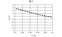
- FIG. 3 is a diagram showing an example of the correspondence between electrode finger pitch (p) and T (thickness of a piezoelectric layer) obtained by the inventor.
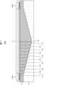
- FIG. 3 is a diagram illustrating an example of the correspondence between T, frequency, and phase obtained by the inventor. It is a figure showing an outline about simulation model SIM1 of an elastic wave device.
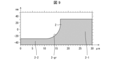
- FIG. 3 is a diagram schematically showing an AFM image of an actually manufactured piezoelectric layer.
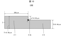
- FIG. 2 is a diagram showing an outline of a simulation model SIM2 of a piezoelectric layer.
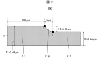
- FIG. 3 is a diagram showing an outline of a simulation model SIM3 of a piezoelectric layer.
- 7 is a diagram illustrating still another configuration example of the elastic wave device in Embodiment 1.
- FIG. 7 is a diagram illustrating still another configuration example of the elastic wave device in Embodiment 1.
- FIG. 7 is a diagram showing an example of the configuration of an elastic wave device in Embodiment 2.
- FIG. 12 is a diagram illustrating a schematic configuration of a communication device in Embodiment 3.
- Embodiment 1 Each elastic wave device according to Embodiment 1 will be described below.
- components having the same functions as the components (components) described in Embodiment 1 are given the same reference numerals in each of the subsequent embodiments, and the description thereof will not be repeated.
- descriptions of known technical matters will be omitted as appropriate.
- Each component, each material, and each numerical value described in this specification is merely an example unless there is a contradiction. Therefore, for example, unless there is a particular contradiction, the positional relationship of each component is not limited to the example shown in each figure. Further, the illustration of each component is not necessarily to scale.
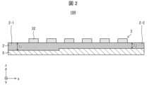
- FIG. 1 is a diagram showing a configuration example of an elastic wave device 100 in the first embodiment.
- FIG. 1 schematically shows a laminated structure of an elastic wave device 100.
- the x direction in the example of the first embodiment is the propagation direction of the elastic wave propagating within the piezoelectric layer 2 of the elastic wave device 100.
- the y direction is an example of a direction intersecting the x direction.
- the z direction is the thickness direction of each member of the elastic wave device 100.
- the positive direction in the z direction is assumed to be an upward direction. Therefore, the negative direction in the z direction is downward.
- the elastic wave device 100 may include at least one resonator 1.
- the elastic wave device 100 includes (i) a support substrate 5, (ii) a piezoelectric layer 2 located on the support substrate 5, and (iii) at least one piezoelectric layer 2 located on the piezoelectric layer 2. It may have an IDT (Interdigital Transducer) electrode 3.
- the IDT electrode 3 is also called an excitation electrode.
- Each of the at least one resonator 1 may share the support substrate 5 and the piezoelectric layer 2.
- each of the at least one resonator 1 may have an individual IDT electrode 3 .
- the elastic wave device 100 may include a pair of reflectors 4a and 4b corresponding to the IDT electrodes 3.
- the reflectors 4a and 4b are also generically referred to as reflectors 4.
- the reflector 4 may be positioned to sandwich the IDT electrode 3 in the x direction.
- any one of the at least one resonator 1 is referred to as a resonator of interest 1A.
- the IDT electrode 3 of the resonator of interest 1A is shown.
- any one of the at least one IDT electrode 3 is referred to as an IDT electrode of interest.
- Embodiment 1 will be described assuming that the IDT electrode 3 of the resonator of interest 1A is the IDT electrode of interest. Therefore, each description of the elastic wave device 100 in Embodiment 1 may be read as a description of the resonator of interest 1A unless there is a particular contradiction.
- the support substrate 5 supports each part of the acoustic wave device 100. Therefore, the support substrate 5 may be located below the piezoelectric layer 2 . As an example, the support substrate 5 may be a Si substrate.
- the piezoelectric layer 2 may be made of a single crystal material having piezoelectricity.
- the material of the piezoelectric layer 2 may be lithium tantalate (also referred to as LiTaO 3 :LT) or lithium niobate (also referred to as LiNbO 3 :LN).
- the piezoelectric layer 2 may be an LT layer.
- the IDT electrode 3 may include, for example, a conductive layer made of metal.
- the metal may be Al.
- the IDT electrode 3 may further include a protective layer covering the conductive layer.
- the material of the protective layer may be TEOS.
- the IDT electrode 3 may have a first bus bar and a second bus bar (not shown in FIG. 1) facing each other in the y direction.
- the IDT electrode 3 includes (i) a plurality of first electrode fingers 32a connected to the first bus bar, and (ii) a plurality of second electrode fingers 32b connected to the second bus bar. good.
- the first electrode finger 32a may extend from the first bus bar toward the second bus bar in the y direction.
- the second electrode finger 32b may extend from the second bus bar toward the first bus bar in the y direction. Therefore, the second electrode finger 32b may be inserted into each of the plurality of first electrode fingers 32a in the y direction (see also FIG. 14, which will be described later).
- the first electrode fingers 32a and the second electrode fingers 32b may be alternately and repeatedly positioned on the piezoelectric layer 2 at approximately constant intervals in the x direction.
- the first electrode finger 32a and the second electrode finger 32b are also generically referred to as electrode fingers 32.
- the electrode finger pitch of the IDT electrode 3 is expressed as p.
- p may be, for example, the pitch (repetition interval) between the centers of two adjacent electrode fingers 32 in the x direction.
- p may be set equal to the half value ( ⁇ /2) of the wavelength ⁇ of the elastic wave excited by the IDT electrode 3.
- the length of the electrode finger 32 in the x direction is referred to as the width w of the electrode finger 32.
- w may be set as appropriate, for example, depending on the electrical characteristics required of the elastic wave device 100.
- w may be set according to p.
- the ratio (w/p) of the width of the electrode finger to the pitch of the electrode finger is referred to as the duty of the electrode finger. By changing the Duty, the frequency characteristics of the elastic wave device 100 can be controlled.
- the maximum thickness of the piezoelectric layer 2 is expressed as Tmax.
- Tmax in Embodiment 1 may be less than or equal to ⁇ .
- the IDT electrode 3 can excite plate waves (Lamb waves) as elastic waves.
- the IDT electrode 3 can excite an A1 mode ram wave as a plate wave. Therefore, in the first embodiment, a case where a plate wave (eg, A1 mode ram wave) propagates within the piezoelectric layer 2 will be exemplified.
- the IDT electrode 3 may excite a bulk wave (thickness shear mode) as an elastic wave.
- the piezoelectric layer 2 includes (i) a first region 2-1 having a first thickness T1, (i) a second region 2-2 having a second thickness T2 smaller than T1, may have.
- T1 is equal to Tmax
- T2 in the first embodiment is smaller than Tmax.
- the thickness of each region of the piezoelectric layer 2 will also be generically referred to as T.
- both the first region 2-1 and the second region 2-2 may be located below the IDT electrode 3 (the IDT electrode of interest). In this way, within one resonator 1, both the first region 2-1 and the second region 2-2 may be located below one IDT electrode 3.
- the height position of the lower surface of the first region 2-1 may match the height position of the lower surface of the second region 2-2.
- the first region 2-1 may protrude upward compared to the second region 2-2.
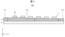
- FIG. 2 and 3 are diagrams each showing another configuration example of the elastic wave device 100.
- the height position of the top surface of the first region 2-1 may match the height position of the top surface of the second region 2-2.
- the first region 2-1 may protrude downward compared to the second region 2-2.
- the piezoelectric layer 2 may further include a third region 2-3 having a third thickness T3 smaller than the second thickness T2.
- the height positions of the lower surfaces of the first area 2-1 to the third area 2-3 may be the same as each other.
- the second region 2-2 may protrude upward compared to the third region 2-3.
- the acoustic wave device may include a piezoelectric layer having a stepped thickness (for convenience, referred to as a "graded piezoelectric layer").
- Piezoelectric layer 2 is an example of a graded piezoelectric layer.
- the main resonance frequency in the elastic wave device 100 may depend on T. Therefore, for example, the main resonant frequency of the plate wave propagating within the first region 2-1 may be different from the main resonant frequency of the plate wave propagating within the second region 2-2.
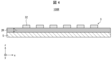
- FIG. 4 is a diagram showing a configuration example of an elastic wave device 100R as a comparative example.
- the elastic wave device 100R is an elastic wave device in which the piezoelectric layer 2 in the elastic wave device according to one aspect of the present disclosure (e.g., the elastic wave device 100 in FIG. 1) is replaced with a piezoelectric layer 2R shown in FIG. 4. .
- the elastic wave device 100R may be referred to as an alternative elastic wave device.
- the piezoelectric layer 2R may be referred to as an alternative piezoelectric layer.
- the piezoelectric layer 2R may have either T1 or T2 having a single thickness T. In the example of FIG. 4, the piezoelectric layer 2R has a single thickness T1.
- the spurious in the elastic wave device (eg, elastic wave device 100) according to one aspect of the present disclosure can be smaller than the spurious in the alternative elastic wave device.
- the elastic wave device according to one aspect of the present disclosure has a graded piezoelectric layer, unlike alternative acoustic wave devices.
- an elastic wave device according to an aspect of the present disclosure may have a smaller number of spurious waves than an alternative elastic wave device.
- the spurious phase (eg, maximum phase value) may be smaller than that in an alternative elastic wave device.
- the spurious in the elastic wave device may be a second harmonic, a third harmonic, and a spurious caused by excitation other than the main resonance. This is because, as described later, the stepped piezoelectric layers can reduce spurious waves caused by excitation of second harmonic waves, third harmonic waves, and main resonance.
- the frequency characteristics of a general elastic wave device may also depend on T. From this, for example, it is expected that the desired frequency characteristics of the elastic wave device can be achieved by controlling T while maintaining the duty constant.
- the main resonant frequency fr of an elastic wave device may depend on p and T. Therefore, as a first preliminary study, the inventor of the present application (hereinafter simply referred to as the "inventor") conducted a simulation and created a plurality of pairs of p and T such that fr in the elastic wave device 100R is 4700 MHz. I explored.
- phase of the impedance of the elastic wave device may also depend on p and T.
- T the phase of the impedance of the elastic wave device
- the inventor determined p corresponding to one predetermined T in the elastic wave device 100R using the above equation (1). Then, the inventor derived phases corresponding to various T's by performing a simulation on the elastic wave device 100R using T and p set as described above.
- FIG. 6 is a contour diagram showing an example of the correspondence between T, frequency, and phase obtained by the inventor.
- the horizontal axis (first axis) in FIG. 6 represents T, and the vertical axis (second axis) represents frequency.
- the height axis (third axis) in FIG. 6 represents phase (degree).
- a phase of ⁇ 90° means that neither resonance nor spurious is present in the phase characteristics of the elastic wave device 100R.
- the phase is sufficiently larger than -90°, it means that a resonance peak or spurious is present in the phase characteristic.
- T 0.44 ⁇ m
- FIG. 7 is a diagram showing an overview of the SIM1. As shown in FIG. 7, SIM1 is symmetrical in the x direction about the line of symmetry SL.
- the piezoelectric layer 2 in the SIM 1 has a first region 2-1 to an eleventh region 2-11. That is, the piezoelectric layer 2 in the SIM 1 has a first thickness T1 to an eleventh thickness T11.
- air layers 9 are located above and below the piezoelectric layer 2, respectively.
- the air layer 9 located below the piezoelectric layer 2 will be referred to as a lower air layer.
- the support substrate 5 located below the lower air layer is omitted.
- the support substrate 5 may be located below the lower air layer. Therefore, for example, the acoustic wave device according to one aspect of the present disclosure may include a membrane structure having a hollow portion surrounded by the support substrate 5 and the piezoelectric layer 2.
- a pair of reflectors 4a and 4b are positioned to sandwich the IDT electrode 3 in the x direction.
- the inventor set the number of electrode fingers of each of the reflectors 4a and 4b to 20 in SIM1.
- p1 represents p in the electrode finger 32 located above the first region 2-1.
- the inventor constructed a simulation model (comparative model) according to a comparative example for comparison with SIM1.
- the comparison model corresponds to the above-described elastic wave device 100R.
- the inventor set the single thickness (Tmax) of the piezoelectric layer 2R in the comparative model to T7 (0.44 ⁇ m).
- the inventor then set p in the comparison model to a single value p7 (1.275 ⁇ m).
- Other conditions in the comparison model are equivalent to SIM1.
- Tmax ⁇ the numerical values for SIM1, also in SIM1, Tmax ⁇ .
- FIG. 8 is a graph showing an example of the phase characteristics of SIM1 and the comparison model derived by simulation.
- the horizontal axis represents frequency
- the vertical axis represents phase.
- both the main resonance frequency and the spurious frequency in the elastic wave device 100 can be controlled.
- the elastic wave device 100 for example, by using a stepped piezoelectric layer, the main resonance frequency and spurious frequency can be controlled while maintaining the pitch and duty of the IDT electrodes 3.
- the pitch and duty of the IDT electrode 3 can be maintained, both the main resonance frequency and the spurious frequency can be appropriately controlled.
- the pitch of the IDT electrode 3 may be controlled as well as the thickness of the piezoelectric layer 2.
- the duty of the IDT electrode 3 may be controlled as well as the thickness of the piezoelectric layer 2.
- FIG. 9 is a diagram schematically showing an AFM image of the manufactured piezoelectric layer 2. As shown in FIG. 9, the manufactured piezoelectric layer 2 is located between the first region 2-1 and the second region 2-2, and the piezoelectric layer 2 is located between the first region 2-1 and the second region 2-2. It has been found that it is possible to have an inclined region 2-gr whose thickness increases toward the 2-1 side.
- SIM2 in FIG. 10 is a first simulation model for the piezoelectric layer 2.
- the piezoelectric layer 2 in the SIM 2 (i) connects the first region 2-1 and the second region 2-2, and (ii) is orthogonal to the first region 2-1 and the second region 2-2. It has a stepped portion 2-ds.
- the piezoelectric layer 2 in the SIM 2 does not have the inclined region 2-gr. Therefore, when moving along the x direction from one of the first region 2-1 and the second region 2-2 to the other, T discontinuously (abruptly) with the stepped portion 2-ds as the boundary. )Change.
- the inventor performed a simulation on SIM2 and derived the stress (more specifically, the maximum principal stress) at point D (lower end position of step portion 2-ds) in FIG. As a result, the stress at point D was 18 MPa.
- SIM3 in FIG. 11 is a second simulation model for the piezoelectric layer 2.
- the piezoelectric layer 2 in the SIM3 has a sloped region 2-gr instead of the stepped portion 2-ds in the SIM2.
- the length of the inclined region 2-gr in the x direction is 5 ⁇ m.
- the inclined region 2-gr in the SIM 3 smoothly connects the first region 2-1 and the second region 2-2 in the z direction (thickness direction, height direction). Therefore, when moving along the x direction from one of the first region 2-1 and the second region 2-2 to the other, T changes continuously (gently) in the inclined region 2-gr. .
- the inventor performed a simulation on SIM3 and derived the stress at point E (upper end position of inclined region 2-gr) and point F (lower end position of inclined region 2-gr) in FIG. As a result, the stress at point E was 7.5 MPa, and the stress at point F was 8 MPa. As described above, the inventor has shown that by providing the sloped region 2-gr in the piezoelectric layer 2, the stress can be reduced to about 40% compared to the case where the sloped region 2-gr is not provided. A new discovery was made through simulation.
- the piezoelectric layer 2 may have a sloped region 2-gr.
- the stress generated at and around the boundary described above can be alleviated. Therefore, it is possible to reduce the possibility that the piezoelectric layer 2 will be damaged due to stress.
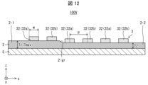
- FIG. 12 is a diagram showing a configuration example of the elastic wave device 100V.
- the elastic wave device 100V is an example of an elastic wave device created based on the above-mentioned knowledge regarding the slope region.
- the elastic wave device 100V is another configuration example of the elastic wave device 100.
- the piezoelectric layer 2 in the acoustic wave device 100V is located between the first region 2-1 and the second region 2-2, and It may have an inclined region 2-gr whose thickness increases toward the 1 region 2-1 side.
- the inclined region 2-gr in the acoustic wave device 100V may have an inclined surface above the piezoelectric layer 2 (that is, on the IDT electrode 3 side). As shown in FIG. 12, the slope may be a downward slope that descends from the first region 2-1 to the second region 2-2.
- the acoustic wave device 100V by having the stepwise piezoelectric layer (the piezoelectric layer 2 having the first region 2-1 and the second region 2-2), spurious is reduced.
- the piezoelectric layer 2 since the piezoelectric layer 2 further includes the inclined region 2-gr, the stress generated in the piezoelectric layer 2 is also alleviated. In this way, according to the acoustic wave device 100V, it is possible to reduce the stress in the piezoelectric layer 2 in addition to reducing spurious waves.
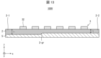
- FIG. 13 is a diagram showing another configuration example of the elastic wave device 100V.
- the inclined region 2-gr in the acoustic wave device 100V may have an inclined surface on the lower side of the piezoelectric layer 2 (ie, on the support substrate 5 side).
- the slope may be an upward slope that rises from the first region 2-1 to the second region 2-2.
- the elastic wave device 100V includes (i) a low acoustic impedance layer having an acoustic impedance lower than that of the piezoelectric layer 2, and (ii) a high acoustic impedance layer having an acoustic impedance higher than that of the piezoelectric layer 2, which are alternately laminated. It may further include a multilayer reflective film.
- the multilayer reflective film may be located between the piezoelectric layer 2 and the support substrate 5.
- the multilayer reflective film may include one or more laminated units formed by laminating one low acoustic impedance layer and one high acoustic impedance layer.
- the multilayer reflective film may include four stacked units. Examples of the material for the low acoustic impedance layer include SiO 2 and the like. Examples of the material for the high acoustic impedance layer include HfO 2 and the like.
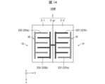
- FIG. 14 is a diagram showing a configuration example of an elastic wave device 100W according to the second embodiment.
- the elastic wave device 100W may include, as the resonator 1, a first resonator 1X and a second resonator 1Y.
- the elastic wave device 100W includes, as the IDT electrodes 3, (i) a first IDT electrode 3X located on the first region 2-1, and (ii) a first IDT electrode 3X located on the second region 2-2. 2IDT electrode 3Y.
- the first resonator 1X may be located on the first region 2-1. Therefore, for example, the first IDT electrode 3X may be the IDT electrode 3 of the first resonator 1X.
- the first IDT electrode 3X may have a plurality of first electrode fingers 32Xa and a plurality of second electrode fingers 32Xb.
- the first electrode finger 32Xa and the second electrode finger 32Xb are also generically referred to as the electrode finger 32X.
- the second resonator 1Y may be located on the second region 2-2. Therefore, for example, the second IDT electrode 3Y may be the IDT electrode 3 of the second resonator 1Y.
- the second IDT electrode 3Y may have a plurality of first electrode fingers 32Ya and a plurality of second electrode fingers 32Yb.
- the first electrode finger 32Ya and the second electrode finger 32Yb are also generically referred to as the electrode finger 32Y.
- the first region 2-1 is located below one resonator (e.g., the first resonator 1X having the first IDT electrode 3X), And (ii) the second region 2-2 may be located below another resonator (eg, the second resonator 1Y having the second IDT electrode 3Y).
- the inclined region 2-gr may be located between the first IDT electrode 3X and the second IDT electrode 3Y in the y direction. In other words, the inclined region 2-gr can be located between the first resonator 1X and the second resonator 1Y in the y direction.
- the elastic wave device 100W may be a ladder filter including a plurality of resonators 1.
- the elastic wave device 100W may include at least one series resonator and at least one parallel resonator as the plurality of resonators 1.
- one of the first resonator 1X or the second resonator 1Y may be a series resonator, and the other may be a parallel resonator.
- both the first resonator 1X and the second resonator 1Y may be series resonators.
- both the first resonator 1X and the second resonator 1Y may be parallel resonators.
- the piezoelectric layer in the acoustic wave device may have N different regions from the first region to the Nth region. .
- N is a natural number of 2 or more.
- the i-th region may have an i-th thickness.
- the i-th thickness will also be referred to as T(i).
- i is a natural number greater than or equal to 1 and less than or equal to N.
- T1 and T2 in FIG. 1 correspond to T(1) and T(2), respectively.
- the alternative piezoelectric layer described above may have any one of N different thicknesses from the first thickness to the Nth thickness as a single thickness.
- the piezoelectric layer has an inclined region located between the i-th region and the (i+1)-th region, and whose thickness increases from the (i+1)-th region toward the i-th region. You may do so. Therefore, the piezoelectric layer may have at most (N-1) different slope regions.
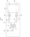
- FIG. 15 is a diagram illustrating a schematic configuration of a communication device 151 in the third embodiment.
- the communication device 151 is an application example of an elastic wave device according to one aspect of the present disclosure, and performs wireless communication using radio waves.
- the communication device 151 may include one duplexer 101 as a transmission filter 109 and another duplexer 101 as a reception filter 111.
- Each of the two duplexers 101 may include an elastic wave device (eg, elastic wave device 100, 100V, or 100W) according to one aspect of the present disclosure.
- the communication device 151 may include an elastic wave device according to one aspect of the present disclosure.
- a transmission information signal TIS containing information to be transmitted is modulated and frequency-increased (converted to a high-frequency signal having a carrier frequency) by an RF-IC (Radio Frequency-Integrated Circuit) 153, and the transmission information signal TIS is converted into a transmission signal. It may be converted to TS.
- the bandpass filter 155 may remove unnecessary components other than the transmission passband for the TS.
- the TS after removing unnecessary components may be amplified by the amplifier 157 and input to the transmission filter 109.
- the transmission filter 109 may remove unnecessary components outside the transmission passband from the input transmission signal TS.
- the transmission filter 109 may output the TS from which unnecessary components have been removed to the antenna 159 via an antenna terminal (eg, TCin described above).
- the antenna 159 may convert the TS, which is an electrical signal input to itself, into a radio wave as a wireless signal, and transmit the radio wave to the outside of the communication device 151.
- the antenna 159 may convert the received radio waves from the outside into a reception signal RS, which is an electrical signal, and input the RS to the reception filter 111 via the antenna terminal.
- the reception filter 111 may remove unnecessary components other than the reception passband from the input RS.
- the reception filter 111 may output the reception signal RS from which unnecessary components have been removed to the amplifier 161.
- the output RS may be amplified by the amplifier 161.
- the bandpass filter 163 may remove unnecessary components other than the receiving passband from the amplified RS.
- the frequency of the RS after unnecessary component removal is lowered and demodulated by the RF-IC 153, and may be converted into a received information signal RIS.
- the TIS and RIS may be low frequency signals (baseband signals) containing appropriate information.
- TIS and RIS may be analog audio signals or digitized audio signals.
- the passband of the wireless signal may be set as appropriate and may conform to various known standards.
- An acoustic wave device includes a support substrate, a piezoelectric layer located on the support substrate, and at least one IDT electrode located on the piezoelectric layer.
- the wavelength ⁇ of the elastic wave excited by the IDT electrode is defined as twice the electrode finger pitch of the IDT electrode, the maximum thickness of the piezoelectric layer is not more than ⁇
- the IDT electrode excites a plate wave or a bulk wave as the elastic wave, and the piezoelectric layer has a first region having a first thickness and a second region having a second thickness smaller than the first thickness. , a sloped region located between the first region and the second region, and whose thickness increases from the second region side toward the first region side. .
- the IDT electrode may excite a plate wave as the elastic wave, and the plate wave may be an A1 mode ram wave.
- the IDT electrode may excite a bulk wave as the elastic wave.
- the main resonance frequency of the plate wave propagating in the first region is the main resonance frequency of the plate wave propagating in the second region. It may be different from the frequency.
- the elastic wave device according to aspect 5 of the present disclosure in any one of aspects 1 to 4, the elastic wave device in which the piezoelectric layer in the acoustic wave device is replaced with an alternative piezoelectric layer is replaced with an alternative elastic wave device.
- the alternative piezoelectric layer has one of the first thickness and the second thickness as a single thickness, and the spurious in the elastic wave device is greater than the spurious in the alternative acoustic wave device. Small is good.
- the spurious in the elastic wave device may be a second harmonic, a third harmonic, and a spurious caused by excitation other than the main resonance.
- the elastic wave device is provided in any one of aspects 1 to 6, wherein at least one of the IDT electrodes includes a first IDT electrode located on the first region, and a second IDT electrode located on the first region. a second IDT electrode located over the region.
- any one of the at least one IDT electrode is referred to as a noted IDT electrode, and the first region and the Both the second region and the second region may be located below the IDT electrode of interest.
- the inclined region may have an inclined surface on the IDT electrode side of the piezoelectric layer.
- the inclined region may have an inclined surface on the support substrate side of the piezoelectric layer.
- the piezoelectric layer further includes a third region having a third thickness smaller than the second thickness. It's fine.
- the acoustic wave device may include a membrane structure having a hollow portion surrounded by the support substrate and the piezoelectric layer in any one of aspects 1 to 11.
- An acoustic wave device includes, in any one of aspects 1 to 12, (i) a low acoustic impedance layer having an acoustic impedance lower than the piezoelectric layer; (ii) the piezoelectric layer It may further include a multilayer reflective film in which high acoustic impedance layers having a higher acoustic impedance than the other layers are alternately laminated.
- the elastic wave device according to aspect 14 of the present disclosure may include the elastic wave device according to any one of aspects 1 to 13 above.
Landscapes
- Physics & Mathematics (AREA)
- Acoustics & Sound (AREA)
- Chemical & Material Sciences (AREA)
- Engineering & Computer Science (AREA)
- Materials Engineering (AREA)
- Surface Acoustic Wave Elements And Circuit Networks Thereof (AREA)
Priority Applications (2)
| Application Number | Priority Date | Filing Date | Title |
|---|---|---|---|
| US18/857,540 US20250279762A1 (en) | 2022-04-22 | 2023-04-18 | Elastic wave device and communication apparatus |
| JP2024516267A JPWO2023204206A1 (cg-RX-API-DMAC7.html) | 2022-04-22 | 2023-04-18 |
Applications Claiming Priority (2)
| Application Number | Priority Date | Filing Date | Title |
|---|---|---|---|
| JP2022-070800 | 2022-04-22 | ||
| JP2022070800 | 2022-04-22 |
Publications (1)
| Publication Number | Publication Date |
|---|---|
| WO2023204206A1 true WO2023204206A1 (ja) | 2023-10-26 |
Family
ID=88419867
Family Applications (1)
| Application Number | Title | Priority Date | Filing Date |
|---|---|---|---|
| PCT/JP2023/015446 Ceased WO2023204206A1 (ja) | 2022-04-22 | 2023-04-18 | 弾性波装置および通信装置 |
Country Status (3)
| Country | Link |
|---|---|
| US (1) | US20250279762A1 (cg-RX-API-DMAC7.html) |
| JP (1) | JPWO2023204206A1 (cg-RX-API-DMAC7.html) |
| WO (1) | WO2023204206A1 (cg-RX-API-DMAC7.html) |
Cited By (1)
| Publication number | Priority date | Publication date | Assignee | Title |
|---|---|---|---|---|
| WO2026049054A1 (ja) * | 2024-09-02 | 2026-03-05 | 株式会社村田製作所 | 弾性波装置 |
Citations (2)
| Publication number | Priority date | Publication date | Assignee | Title |
|---|---|---|---|---|
| WO2010004741A1 (ja) * | 2008-07-11 | 2010-01-14 | パナソニック株式会社 | 板波素子と、これを用いた電子機器 |
| JP2016072808A (ja) * | 2014-09-30 | 2016-05-09 | 株式会社村田製作所 | デュプレクサ及びその製造方法 |
-
2023
- 2023-04-18 JP JP2024516267A patent/JPWO2023204206A1/ja active Pending
- 2023-04-18 US US18/857,540 patent/US20250279762A1/en active Pending
- 2023-04-18 WO PCT/JP2023/015446 patent/WO2023204206A1/ja not_active Ceased
Patent Citations (2)
| Publication number | Priority date | Publication date | Assignee | Title |
|---|---|---|---|---|
| WO2010004741A1 (ja) * | 2008-07-11 | 2010-01-14 | パナソニック株式会社 | 板波素子と、これを用いた電子機器 |
| JP2016072808A (ja) * | 2014-09-30 | 2016-05-09 | 株式会社村田製作所 | デュプレクサ及びその製造方法 |
Cited By (1)
| Publication number | Priority date | Publication date | Assignee | Title |
|---|---|---|---|---|
| WO2026049054A1 (ja) * | 2024-09-02 | 2026-03-05 | 株式会社村田製作所 | 弾性波装置 |
Also Published As
| Publication number | Publication date |
|---|---|
| US20250279762A1 (en) | 2025-09-04 |
| JPWO2023204206A1 (cg-RX-API-DMAC7.html) | 2023-10-26 |
Similar Documents
| Publication | Publication Date | Title |
|---|---|---|
| US11962283B2 (en) | Piston mode lamb wave resonators | |
| Lu et al. | Enabling higher order Lamb wave acoustic devices with complementarily oriented piezoelectric thin films | |
| US11128279B2 (en) | Acoustic wave resonator, acoustic wave filter, multiplexer, communication apparatus, and method designing acoustic wave resonator | |
| EP1892832B1 (en) | Multi-mode thin film elastic wave resonator filter | |
| JP6530494B2 (ja) | 弾性表面波素子 | |
| KR20180012787A (ko) | 탄성파 필터, 멀티플렉서, 듀플렉서, 고주파 프론트 엔드 회로, 및 통신장치 | |
| JP2003332874A (ja) | 弾性表面波フィルタ,平衡型回路,および通信装置 | |
| US20230396233A1 (en) | Surface acoustic wave devices having reduced size | |
| JP7793060B2 (ja) | 弾性波共振子、弾性波フィルタおよび通信装置 | |
| JP2025518169A (ja) | 高速高次モードを有する弾性表面波デバイス | |
| JP2024153900A (ja) | 弾性波共振子、弾性波フィルタ、分波器、通信装置 | |
| US20250279762A1 (en) | Elastic wave device and communication apparatus | |
| US20240356522A1 (en) | Elastic wave element, demultiplexer, and communication device | |
| US20250105822A1 (en) | Filter device, splitter, and communication device | |
| JP7791994B2 (ja) | 弾性波装置および通信装置 | |
| US20250192753A1 (en) | Elastic wave filter, demultiplexer, and communication apparatus | |
| JP3733020B2 (ja) | 圧電素子およびそれを用いた移動体通信装置 | |
| JP7797713B2 (ja) | 弾性波フィルタおよび通信装置 | |
| JP7801372B2 (ja) | 弾性波フィルタおよび通信装置 | |
| WO2025053101A1 (ja) | 弾性波装置および通信装置 | |
| JP2025179286A (ja) | 弾性波共振子および通信装置 | |
| JP2024163800A (ja) | フィルタおよび通信装置 | |
| WO2024190677A1 (ja) | 弾性波共振子および通信装置 | |
| JP2025038691A (ja) | フィルタおよび通信装置 | |
| WO2025063205A1 (ja) | 弾性波装置、および通信装置 |
Legal Events
| Date | Code | Title | Description |
|---|---|---|---|
| 121 | Ep: the epo has been informed by wipo that ep was designated in this application |
Ref document number: 23791854 Country of ref document: EP Kind code of ref document: A1 |
|
| WWE | Wipo information: entry into national phase |
Ref document number: 2024516267 Country of ref document: JP |
|
| NENP | Non-entry into the national phase |
Ref country code: DE |
|
| 122 | Ep: pct application non-entry in european phase |
Ref document number: 23791854 Country of ref document: EP Kind code of ref document: A1 |
|
| WWP | Wipo information: published in national office |
Ref document number: 18857540 Country of ref document: US |