WO2023199860A1 - 高周波モジュール、通信装置及びフィルタ - Google Patents
高周波モジュール、通信装置及びフィルタ Download PDFInfo
- Publication number
- WO2023199860A1 WO2023199860A1 PCT/JP2023/014386 JP2023014386W WO2023199860A1 WO 2023199860 A1 WO2023199860 A1 WO 2023199860A1 JP 2023014386 W JP2023014386 W JP 2023014386W WO 2023199860 A1 WO2023199860 A1 WO 2023199860A1
- Authority
- WO
- WIPO (PCT)
- Prior art keywords
- resonator
- chip
- conductor
- substrate
- input
- Prior art date
- Legal status (The legal status is an assumption and is not a legal conclusion. Google has not performed a legal analysis and makes no representation as to the accuracy of the status listed.)
- Ceased
Links
Images












Classifications
-
- H—ELECTRICITY
- H03—ELECTRONIC CIRCUITRY
- H03H—IMPEDANCE NETWORKS, e.g. RESONANT CIRCUITS; RESONATORS
- H03H9/00—Networks comprising electromechanical or electro-acoustic elements; Electromechanical resonators
- H03H9/46—Filters
- H03H9/54—Filters comprising resonators of piezoelectric or electrostrictive material
- H03H9/56—Monolithic crystal filters
- H03H9/566—Electric coupling means therefor
- H03H9/568—Electric coupling means therefor consisting of a ladder configuration
-
- H—ELECTRICITY
- H03—ELECTRONIC CIRCUITRY
- H03H—IMPEDANCE NETWORKS, e.g. RESONANT CIRCUITS; RESONATORS
- H03H9/00—Networks comprising electromechanical or electro-acoustic elements; Electromechanical resonators
- H03H9/02—Details
- H03H9/125—Driving means, e.g. electrodes, coils
- H03H9/145—Driving means, e.g. electrodes, coils for networks using surface acoustic waves
-
- H—ELECTRICITY
- H03—ELECTRONIC CIRCUITRY
- H03H—IMPEDANCE NETWORKS, e.g. RESONANT CIRCUITS; RESONATORS
- H03H9/00—Networks comprising electromechanical or electro-acoustic elements; Electromechanical resonators
- H03H9/25—Constructional features of resonators using surface acoustic waves
-
- H—ELECTRICITY
- H03—ELECTRONIC CIRCUITRY
- H03H—IMPEDANCE NETWORKS, e.g. RESONANT CIRCUITS; RESONATORS
- H03H9/00—Networks comprising electromechanical or electro-acoustic elements; Electromechanical resonators
- H03H9/46—Filters
- H03H9/64—Filters using surface acoustic waves
-
- H—ELECTRICITY
- H03—ELECTRONIC CIRCUITRY
- H03H—IMPEDANCE NETWORKS, e.g. RESONANT CIRCUITS; RESONATORS
- H03H9/00—Networks comprising electromechanical or electro-acoustic elements; Electromechanical resonators
- H03H9/46—Filters
- H03H9/64—Filters using surface acoustic waves
- H03H9/6423—Means for obtaining a particular transfer characteristic
- H03H9/6433—Coupled resonator filters
- H03H9/6483—Ladder SAW filters
-
- H—ELECTRICITY
- H03—ELECTRONIC CIRCUITRY
- H03H—IMPEDANCE NETWORKS, e.g. RESONANT CIRCUITS; RESONATORS
- H03H9/00—Networks comprising electromechanical or electro-acoustic elements; Electromechanical resonators
- H03H9/70—Multiple-port networks for connecting several sources or loads, working on different frequencies or frequency bands, to a common load or source
- H03H9/72—Networks using surface acoustic waves
- H03H9/725—Duplexers
-
- H—ELECTRICITY
- H04—ELECTRIC COMMUNICATION TECHNIQUE
- H04B—TRANSMISSION
- H04B1/00—Details of transmission systems, not covered by a single one of groups H04B3/00 - H04B13/00; Details of transmission systems not characterised by the medium used for transmission
- H04B1/38—Transceivers, i.e. devices in which transmitter and receiver form a structural unit and in which at least one part is used for functions of transmitting and receiving
-
- H—ELECTRICITY
- H05—ELECTRIC TECHNIQUES NOT OTHERWISE PROVIDED FOR
- H05K—PRINTED CIRCUITS; CASINGS OR CONSTRUCTIONAL DETAILS OF ELECTRIC APPARATUS; MANUFACTURE OF ASSEMBLAGES OF ELECTRICAL COMPONENTS
- H05K1/00—Printed circuits
- H05K1/02—Details
- H05K1/0213—Electrical arrangements not otherwise provided for
- H05K1/0237—High frequency adaptations
- H05K1/0243—Printed circuits associated with mounted high frequency components
-
- H—ELECTRICITY
- H05—ELECTRIC TECHNIQUES NOT OTHERWISE PROVIDED FOR
- H05K—PRINTED CIRCUITS; CASINGS OR CONSTRUCTIONAL DETAILS OF ELECTRIC APPARATUS; MANUFACTURE OF ASSEMBLAGES OF ELECTRICAL COMPONENTS
- H05K1/00—Printed circuits
- H05K1/02—Details
- H05K1/11—Printed elements for providing electric connections to or between printed circuits
- H05K1/115—Via connections; Lands around holes or via connections
-
- H—ELECTRICITY
- H05—ELECTRIC TECHNIQUES NOT OTHERWISE PROVIDED FOR
- H05K—PRINTED CIRCUITS; CASINGS OR CONSTRUCTIONAL DETAILS OF ELECTRIC APPARATUS; MANUFACTURE OF ASSEMBLAGES OF ELECTRICAL COMPONENTS
- H05K2201/00—Indexing scheme relating to printed circuits covered by H05K1/00
- H05K2201/10—Details of components or other objects attached to or integrated in a printed circuit board
- H05K2201/10007—Types of components
- H05K2201/1006—Non-printed filter
Definitions
- the present invention generally relates to a high frequency module, a communication device, and a filter, and more particularly relates to a high frequency module including a filter, a communication device including the same, and a filter.
- Patent Document 1 discloses a series resonator, a first wafer on which the series resonator is arranged, a parallel resonator connected between the series resonator and the ground, and a second wafer on which the parallel resonator is arranged.
- a filter circuit includes: a plurality of solder balls connecting a second wafer and a substrate (mounted substrate); and a plurality of wafer vias arranged on the second wafer and connected to the plurality of solder balls.
- One of the wafer vias arranged on both sides of the second wafer is connected to an input terminal, and the other is connected to an output terminal.
- inductive coupling occurs between the path between the mounting board and the series arm resonator of the filter, and the path between the filter's parallel arm resonator and the mounting board. properties may deteriorate.
- An object of the present invention is to provide a high frequency module, a communication device, and a filter that can suppress deterioration of filter characteristics.
- a high frequency module includes a mounting board and a filter.
- the mounting board has a first conductor part, a second conductor part, and a ground conductor part.
- the filter is arranged on the mounting board.
- the filter includes a first input/output terminal, a second input/output terminal, a ground terminal, a series arm resonator, and a parallel arm resonator.
- the first input/output terminal, the second input/output terminal, and the ground terminal are connected to the first conductor section, the second conductor section, and the ground conductor section, respectively.
- the series arm resonator is provided in a signal path between the first input/output terminal and the second input/output terminal, and is closest to the first input/output terminal or the second input/output terminal.
- the parallel arm resonator is connected between the signal path and the ground conductor, and is closest to the series arm resonator.
- a first chip is placed on the mounting board, and a second chip is placed on the first chip.
- the first chip includes a first resonator that is one of the series arm resonator and the parallel arm resonator.
- the second chip includes a second resonator that is the remaining of the series arm resonator and the parallel arm resonator.
- the filter has a first connecting conductor part and a second connecting conductor part.
- the first connection conductor part and the second connection conductor part are interposed between the first chip and the second chip in the thickness direction of the mounting board.
- the first chip includes a first through-via conductor, a second through-via conductor, a first wiring section, and a second wiring section.
- the first through-via conductor is interposed between the first terminal and the first connection conductor.
- the first terminal is one of the first input/output terminal and the second input/output terminal that is closest to the series arm resonator, and the ground terminal.
- the second through-via conductor is connected to a second terminal.
- the second terminal is the remaining one of the first input/output terminal and the second input/output terminal that is closest to the series arm resonator and the ground terminal.
- the first wiring section connects the second connection conductor section and the first resonator.
- the second wiring section connects the first resonator and the second through via conductor.
- the second chip includes a third wiring section and a fourth wiring section.
- the third wiring section connects the first connection conductor section and the second resonator.
- the fourth wiring section connects the second resonator and the second connection conductor section.
- a distance between the second through-via conductor and the first through-via conductor is shorter than a distance between the first wiring section and the first through-via conductor.
- a high frequency module includes a mounting board and a filter.
- the mounting board has a first conductor part, a second conductor part, and a ground conductor part.
- the filter is arranged on the mounting board.
- the filter includes a first input/output terminal, a second input/output terminal, a ground terminal, a series arm resonator, and a parallel arm resonator.
- the first input/output terminal, the second input/output terminal, and the ground terminal are connected to the first conductor section, the second conductor section, and the ground conductor section, respectively.
- the series arm resonator is provided in a signal path between the first input/output terminal and the second input/output terminal, and is closest to the first input/output terminal or the second input/output terminal.
- the parallel arm resonator is connected between the signal path and the ground conductor, and is closest to the series arm resonator.
- a first chip is placed on the mounting board, and a second chip is placed on the first chip.
- the first chip includes a first resonator that is one of the series arm resonator and the parallel arm resonator.
- the second chip includes a second resonator that is the remaining of the series arm resonator and the parallel arm resonator.
- the filter has a first connecting conductor part and a second connecting conductor part.
- the first connection conductor part and the second connection conductor part are interposed between the first chip and the second chip in the thickness direction of the mounting board.
- the first chip includes a first through-via conductor, a second through-via conductor, a first wiring section, and a second wiring section.
- the first through-via conductor is interposed between the first terminal and the first connection conductor.
- the first terminal is one of the first input/output terminal and the second input/output terminal that is closest to the series arm resonator, and the ground terminal.
- the second through-via conductor is connected to a second terminal.
- the second terminal is the remaining one of the first input/output terminal and the second input/output terminal that is closest to the series arm resonator and the ground terminal.
- the first wiring section connects the second connection conductor section and the first resonator.
- the second wiring section connects the first resonator and the second through via conductor.
- the second chip includes a third wiring section and a fourth wiring section.
- the third wiring section connects the first connection conductor section and the second resonator.
- the fourth wiring section connects the second resonator and the second connection conductor section.
- a communication device includes the above-mentioned high frequency module and a signal processing circuit.
- the signal processing circuit is connected to the high frequency module.
- a filter according to one aspect of the present invention is a filter placed on a mounting board.
- the filter includes a first input/output terminal, a second input/output terminal, a ground terminal, a series arm resonator, and a parallel arm resonator.
- the first input/output terminal, the second input/output terminal, and the ground terminal are respectively connected to a first conductor part, a second conductor part, and a ground conductor part included in the mounting board.
- the series arm resonator is provided in a signal path between the first input/output terminal and the second input/output terminal, and is closest to the first input/output terminal or the second input/output terminal.
- the parallel arm resonator is connected between the signal path and the ground conductor, and is closest to the series arm resonator.
- a first chip and a second chip are stacked.
- the first chip includes a first resonator that is one of the series arm resonator and the parallel arm resonator.
- the second chip includes a second resonator that is the remaining of the series arm resonator and the parallel arm resonator.
- the first resonator and the second resonator face each other in the thickness direction of the first chip.
- the filter has a first connecting conductor part and a second connecting conductor part. The first connecting conductor part and the second connecting conductor part are interposed between the first chip and the second chip in the thickness direction of the first chip.
- the first chip includes a first through-via conductor, a second through-via conductor, a first wiring section, and a second wiring section.
- the first through-via conductor is interposed between the first terminal and the first connection conductor.
- the first terminal is one of the first input/output terminal and the second input/output terminal that is closest to the series arm resonator, and the ground terminal.
- the second through-via conductor is connected to a second terminal.
- the second terminal is the remaining one of the first input/output terminal and the second input/output terminal that is closest to the series arm resonator and the ground terminal.
- the first wiring section connects the second connection conductor section and the first resonator.
- the second wiring section connects the first resonator and the second through via conductor.
- the second chip includes a third wiring section and a fourth wiring section.
- the third wiring section connects the first connection conductor section and the second resonator.
- the fourth wiring section connects the second resonator and the second connection conductor section. A distance between the second through-via conductor and the first through-via conductor is shorter than a distance between the first wiring section and the first through-via conductor.
- the high frequency module, communication device, and filter according to the above aspects of the present invention can suppress deterioration of filter characteristics.
- FIG. 1 is a sectional view of a high frequency module according to a first embodiment.
- FIG. 2 is an explanatory diagram of a current loop path in the high frequency module same as above.
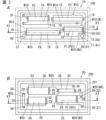
- FIG. 3A is a perspective view of the top surface of the first chip in the same high-frequency module as seen from the bottom surface side of the first chip.
- FIG. 3B is a bottom view of the second chip in the high frequency module same as above.
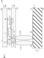
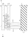
- FIG. 4 is a schematic cross-sectional view corresponding to the cross section taken along the line X1-X1 in FIGS. 3A and 3B regarding the filter in the high-frequency module.
- FIG. 5 is a circuit diagram of a filter in the high frequency module same as above.
- FIG. 5 is a circuit diagram of a filter in the high frequency module same as above.
- FIG. 6 is a circuit explanatory diagram of a filter in the high frequency module same as above.
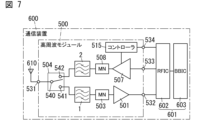
- FIG. 7 is a circuit configuration diagram of a communication device including the same high frequency module as above.
- FIG. 8 is a sectional view of a high frequency module according to Modification 1 of Embodiment 1.
- FIG. 9 is a sectional view of a high frequency module according to a second modification of the first embodiment.
- FIG. 10 is a sectional view of a high frequency module according to a third modification of the first embodiment.
- FIG. 11 is a sectional view of a high frequency module according to a fourth modification of the first embodiment.
- FIG. 12 is a circuit diagram of a filter in a high frequency module according to a fifth modification of the first embodiment.
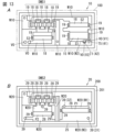
- FIG. 13A is a perspective view of the upper surface of the first chip in the same high-frequency module as seen from the lower surface side of the first chip.
- FIG. 13B is a bottom view of the second chip in the high frequency module same as above.
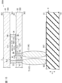
- FIG. 14 is a sectional view of the high frequency module according to the second embodiment.
- FIG. 15 is another cross-sectional view of the high frequency module same as above.
- FIG. 16 is a circuit diagram of a first filter and a second filter in the high frequency module same as above.
- FIG. 17 is an explanatory diagram of current loop paths of each of the first filter and the second filter in the high frequency module same as above.
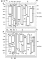
- FIG. 18A is a perspective view of the top surfaces of the first chip and the third chip in the high frequency module according to Modification 1 of Embodiment 2, seen from below.
- FIG. 18B is a bottom view of the second chip and the fourth chip in the high frequency module same as above.
- FIG. 19A is a perspective view of the upper surfaces of the first chip and the third chip in the high frequency module according to Modification Example 2 of Embodiment 2, seen from the lower surface side.
- FIG. 19B is a bottom view of the second chip and the fourth chip in the high frequency module same as above.
- FIG. 20 is a circuit diagram of a first filter and a second filter of a high frequency module according to a third modification of the second embodiment.
- FIG. 21A is a perspective view of the upper surfaces of the first chip and the third chip in the high-frequency module same as above, seen from the lower surface side.
- FIG. 21B is a bottom view of the second chip and the fourth chip in the high frequency module same as above.
- FIG. 22A is a perspective view of the top surface of the first chip in the high-frequency module according to Embodiment 3, seen from the bottom surface side of the first chip.
- FIG. 22B is a bottom view of the second chip in the high frequency module same as above.
- the high frequency module 500 includes a mounting board 9 and a filter 1, as shown in FIG.
- the filter 1 includes, for example, a plurality of (for example, eight) elastic wave resonators.
- the plurality of elastic wave resonators include, for example, as shown in FIG. 5, four series arm resonators S1, S2, S3, and S4, and four parallel arm resonators P1, P2, P3, and P4.
- each of the three series arm resonators S1, S3, and S4 among the four series arm resonators S1, S2, S3, and S4 is formed by a plurality of (for example, two) split resonators. configured, but not limited to this.
- a plurality of split resonators is a resonator in which one elastic wave resonator is split, and there is no intervening other elastic wave resonators between the split resonators, and other elastic wave resonators are not interposed between the split resonators. They are connected in series with the included paths without any connection nodes.
- the mounting board 9 has a first conductor part 901, a second conductor part (not shown), and a ground conductor part 905.
- Filter 1 is placed on mounting board 9 .
- the filter 1 includes a first input/output terminal T1, a second input/output terminal T2 (see FIGS. 3A and 5), a ground terminal T5, a series arm resonator S01, and a parallel arm resonator P01.
- the first input/output terminal T1, the second input/output terminal T2, and the ground terminal T5 are connected to the first conductor section 901, the second conductor section (not shown), and the ground conductor section 905, respectively.
- the series arm resonator S01 is provided in the signal path Ru1 (see FIG.
- the parallel arm resonator P01 is connected between the signal path Ru1 and the ground conductor section 905, and is the parallel arm closest to the series arm resonator S01 among the plurality of parallel arm resonators P1, P2, P3, and P4. This is the resonator P1 (see FIG. 5).
- the first chip 10 is placed on the mounting board 9, and the second chip 20 is placed on the first chip 10.
- the first chip 10 has a first resonator 11 that is one of a series arm resonator S01 and a parallel arm resonator P01.
- the second chip 20 has the second resonator 12 that is the remaining of the series arm resonator S01 and the parallel arm resonator P01.
- the first resonator 11 and the second resonator 12 face each other in the thickness direction D1 of the mounting board 9.
- the filter 1 has a first connecting conductor part 31 and a second connecting conductor part 32.
- the first connecting conductor part 31 and the second connecting conductor part 32 are interposed between the first chip 10 and the second chip 20 in the thickness direction D1 of the mounting board 9.
- the first chip 10 includes a first through-via conductor V1, a second through-via conductor V2, a first wiring section W1, and a second wiring section W2.
- the first through via conductor V1 is interposed between the first terminal 41 and the first connection conductor portion 31 in the thickness direction D1 of the mounting board 9.
- the first through via conductor V1 and the first terminal 41 only need to be electrically connected to each other in the first chip 10, and the first through via conductor V1 and the first terminal 41 need only be electrically connected to each other in the first chip 10. It is not essential that they overlap.
- the first terminal 41 is the first input/output terminal T1.
- the second through via conductor V2 overlaps the second terminal 42 in the thickness direction D1 of the mounting board 9.
- the second through via conductor V2 only needs to be electrically connected to the second terminal 42 in the first chip 10, and the second through via conductor V2 and the second terminal 42 are connected in the thickness direction D1 of the mounting board 9. It is not essential that they overlap.
- the second terminal 42 is a ground terminal T5.
- the first wiring section W1 connects the second connection conductor section 32 and the first resonator 11.
- the second wiring portion W2 connects the first resonator 11 and the second through via conductor V2.
- the second chip 20 includes a third wiring section W3 and a fourth wiring section W4.
- the third wiring section W3 connects the first connection conductor section 31 and the second resonator 12.
- the fourth wiring portion W4 connects the second resonator 12 and the second connection conductor portion 32.
- the distance Le2 between the second through-via conductor V2 and the first through-via conductor V1 is shorter than the distance Le1 between the first wiring portion W1 and the first through-via conductor V1.
- a current loop path Ro1 is formed as indicated by a thick arrow in FIG.
- the current loop path Ro1 is the first conductor section 901-first terminal 41-first through via conductor V1-first connection conductor section 31-third wiring section W3-second resonator 12-fourth wiring section W4-first 2-connection conductor section 32 - first wiring section W1 - first resonator 11 - second wiring section W2 - second through via conductor V2 - second terminal 42 - ground conductor section 905.
- the first conductor section 901 and the ground conductor section 905 are separated, since there is a potential difference between the first conductor section 901 and the ground conductor section 905, a part of the current loop path Ro1 is connected to the ground conductor section 905. - includes the path of the first conductor section 901;
- the distance H2 between the second wiring part W2 and the ground conductor part 905 is the same as the distance H1 between the first wiring part W1 and the fourth wiring part W4. longer than
- the high frequency module 500 is used, for example, in a communication device 600, as shown in FIG.
- the communication device 600 is, for example, a mobile phone (for example, a smartphone), but is not limited thereto, and may be, for example, a wearable terminal (for example, a smart watch).
- the high frequency module 500 is a module that is compatible with, for example, the 4G (fourth generation mobile communication) standard, the 5G (fifth generation mobile communication) standard, and the like.
- the 4G standard is, for example, the 3GPP (registered trademark, Third Generation Partnership Project) and LTE (registered trademark, Long Term Evolution) standard.
- the 5G standard is, for example, 5G NR (New Radio).
- the communication device 600 includes a high frequency module 500 and a signal processing circuit 601. Communication device 600 further includes an antenna 610.
- the communication device 600 further includes a circuit board (not shown) on which the high frequency module 500 is mounted.
- the circuit board is, for example, a printed wiring board.
- the circuit board has a ground electrode to which a ground potential is applied.
- the high frequency module 500 is configured to be able to amplify a received signal input from an antenna 610 and output it to the signal processing circuit 601, for example. Furthermore, the high frequency module 500 is configured to be able to amplify a transmission signal input from the signal processing circuit 601 and output the amplified signal to the antenna 610, for example.
- the signal processing circuit 601 is not a component of the high frequency module 500 but a component of the communication device 600 including the high frequency module 500.
- the high frequency module 500 is controlled by, for example, a signal processing circuit 601 included in the communication device 600.
- the high frequency module 500 includes a filter 1 (hereinafter also referred to as first filter 1), a second filter 2, a low noise amplifier 501, an input matching circuit 503, a power amplifier 507, and an output matching circuit 503. It includes a circuit 508, a controller 515, and a switch 504.
- the first filter 1 constitutes a reception filter.
- the second filter 2 constitutes a transmission filter.
- the high frequency module 500 includes a plurality of external connection terminals.
- the plurality of external connection terminals include an antenna terminal 531, a signal output terminal 532, a signal input terminal 533, a plurality of control terminals 534 (only one is shown in Fig. 7), and a plurality of external ground terminals (Fig. (not shown).
- the plurality of external ground terminals are terminals to which a ground potential is applied.
- the first filter 1 is, for example, a filter whose passband is the reception band of the first communication band.
- the first communication band is, for example, a communication band of the 3GPP LTE standard or a communication band of the 5G NR standard.
- the first communication band is, for example, Band 25 of the 3GPP LTE standard or n25 of the 5G NR standard.
- the first communication band is a communication band used for communication compatible with FDD (Frequency Division Duplex) as a communication method, but is not limited to this, a communication band used for communication compatible with TDD (Time Division Duplex). It may be.
- the second filter 2 is, for example, a filter whose passband is the transmission band of the second communication band.
- the second communication band is, for example, Band 25 of the 3GPP LTE standard or n25 of the 5G NR standard.
- the second communication band is a communication band used for communication compatible with FDD as a communication method, but is not limited to this, and may be a communication band used for communication compatible with TDD.
- the second communication band is the same communication band as the first communication band, which is Band 25 of the 3GPP LTE standard or n25 of the 5G NR standard, but a communication band different from the first communication band. It may be a band.
- the low noise amplifier 501 has an input terminal and an output terminal.
- the low noise amplifier 501 amplifies a received signal input to an input terminal and outputs the amplified signal from an output terminal.
- the output terminal of low noise amplifier 501 is connected to signal output terminal 532.
- the output terminal of the low noise amplifier 501 is connected to the signal processing circuit 601 via a signal output terminal 532, for example.
- the signal output terminal 532 is a terminal for outputting a high frequency signal (received signal) from the low noise amplifier 501 to an external circuit (for example, the signal processing circuit 601).
- the input matching circuit 503 is provided in the signal path between the first filter 1 and the input terminal of the low noise amplifier 501.
- the input matching circuit 503 is a circuit for impedance matching between the first filter 1 and the low noise amplifier 501, and includes, for example, one inductor.
- Input matching circuit 503 is not limited to including one inductor, and may include, for example, multiple inductors and multiple capacitors.
- the power amplifier 507 has an input terminal and an output terminal. Power amplifier 507 amplifies the transmission signal input to the input terminal and outputs the amplified signal from the output terminal.
- An input terminal of power amplifier 507 is connected to signal input terminal 533.
- An input terminal of power amplifier 507 is connected to signal processing circuit 601 of communication device 600 via signal input terminal 533.
- the signal input terminal 533 is a terminal for inputting a high frequency signal (transmission signal) from an external circuit (for example, the signal processing circuit 601) to the high frequency module 500.
- the output terminal of the power amplifier 507 is connected to the switch 504 via the output matching circuit 508 and the second filter 2.
- the output matching circuit 508 is provided in the signal path between the output terminal of the power amplifier 507 and the second filter 2.
- the output matching circuit 508 is a circuit for impedance matching between the power amplifier 507 and the second filter 2, and includes, for example, a plurality of inductors and a plurality of capacitors.
- the controller 515 controls the power amplifier 507. Controller 515 controls power amplifier 507 according to a control signal from signal processing circuit 601, for example.
- the controller 515 is connected to the signal processing circuit 601 via a plurality of (for example, four) control terminals 534.
- the number of control terminals 534 is, for example, four, but only one is shown in FIG.
- the plurality of control terminals 534 are terminals for inputting control signals from an external circuit (for example, the signal processing circuit 601) to the controller 515.
- Controller 515 controls power amplifier 507 based on control signals acquired from signal processing circuit 601 via a plurality of control terminals 534.
- the control signal acquired by controller 515 is a digital signal.
- the switch 504 has a common terminal 540 and a plurality of (for example, two) selection terminals 541 and 542.
- common terminal 540 is connected to antenna terminal 531.
- the selection terminal 541 is connected to the first filter 1 .
- the selection terminal 542 is connected to the second filter 2.
- the switch 504 is, for example, a switch that can connect one or more of the plurality of selection terminals 541 and 542 to the common terminal 540.
- the switch 504 is, for example, a switch capable of one-to-one and one-to-many connections. Switch 504 is controlled by signal processing circuit 601, for example.
- the switch 504 switches the connection state between the common terminal 540 and the plurality of selection terminals 541 and 542 according to a control signal from the RF signal processing circuit 602 of the signal processing circuit 601.
- the switch 504 is, for example, a switch IC (Integrated Circuit).
- the first filter 1 includes an elastic wave filter having a plurality of elastic wave resonators.
- the elastic wave filter included in the first filter 1 is, for example, a ladder type filter.
- the plurality of elastic wave resonators include, for example, as shown in FIG. 5, four series arm resonators S1, S2, S3, and S4, and four parallel arm resonators P1, P2, P3, and P4.
- the four series arm resonators S1, S2, S3, and S4 are provided on a first signal path Ru1 (hereinafter also referred to as series arm path Ru1) between the first input/output terminal T1 and the second input/output terminal T2.
- the four series arm resonators S1, S2, S3, and S4 are connected in series on the series arm path Ru1.
- the series arm resonator S1, the series arm resonator S2, the series arm resonator S3, and the series arm resonator S4 are connected to the series arm resonator from the first input/output terminal T1 side.
- S1, series arm resonator S2, series arm resonator S3, and series arm resonator S4 are arranged in this order.
- the parallel arm resonator P1 is provided on a path Ru11 (hereinafter also referred to as parallel arm path Ru11) between the path between the series arm resonator S1 and the series arm resonator S2 in the series arm path Ru1 and the ground. ing.
- the parallel arm resonator P2 is provided on a route Ru12 (hereinafter also referred to as parallel arm route Ru12) between the series arm resonator S2 and the series arm resonator S3 in the series arm route Ru1 and the ground. There is.
- the parallel arm resonator P3 is provided on a path Ru13 (hereinafter also referred to as parallel arm path Ru13) between the path between the series arm resonator S3 and the series arm resonator S4 in the series arm path Ru1 and the ground. ing.
- the parallel arm resonator P4 is connected to a path Ru14 (hereinafter also referred to as parallel arm path Ru14) between the series arm resonator S4 and the second input/output terminal T2 in the series arm path Ru1 and the ground. It is set in.
- the series arm resonator S1 is provided in the signal path Ru1 between the first input/output terminal T1 and the second input/output terminal T2, and is connected to the first input/output terminal T1 or the second input/output terminal. It constitutes the closest series arm resonator S01 (hereinafter also referred to as first series arm resonator S01).
- the first series arm resonator S01 is the series arm resonator closest to the first input/output terminal T1 among the plurality of series arm resonators S1, S2, S3, and S4. .
- the series arm resonator S01 closest to the first input/output terminal T1 is a series arm resonator connected to the first input/output terminal T1 without going through another series arm resonator.
- the series arm resonator S01 closest to the first input/output terminal T1 is the series arm resonator electrically closest to the first input/output terminal T1 regardless of physical distance.
- the parallel arm resonator P1 is connected between the signal path Ru1 and the ground conductor section 905 (see FIG. 1).
- the ground conductor portion 905 is connected to the external ground terminal of the mounting board 9. In the high frequency module 500, as shown in FIG.
- the parallel arm resonator P01 constitutes the parallel arm resonator P01 (hereinafter also referred to as the first parallel arm resonator P01) closest to the series arm resonator S01. .
- the ground conductor portion 905 is connected to the external ground terminal of the mounting board 9.
- "Parallel arm resonator P01 closest to series arm resonator S01” is a parallel arm resonator that is connected to series arm resonator S01 without going through another series arm resonator or another parallel arm resonator. .
- parallel arm resonator P01 closest to series arm resonator S01 is the parallel arm resonator electrically closest to series arm resonator S01 regardless of physical distance.
- the communication device 600 includes a high frequency module 500 and a signal processing circuit 601. Signal processing circuit 601 is connected to high frequency module 500. Communication device 600 further includes an antenna 610. Communication device 600 further includes a circuit board on which high frequency module 500 is mounted.
- the circuit board is, for example, a printed wiring board.
- the circuit board has a ground electrode to which a ground potential is applied.
- the signal processing circuit 601 includes, for example, an RF signal processing circuit 602 and a baseband signal processing circuit 603.
- the RF signal processing circuit 602 is, for example, an RFIC (Radio Frequency Integrated Circuit), and performs signal processing on high frequency signals.
- the RF signal processing circuit 602 performs signal processing such as up-conversion on the high frequency signal (transmission signal) output from the baseband signal processing circuit 603, and outputs the high frequency signal subjected to the signal processing. Further, the RF signal processing circuit 602 performs signal processing such as down-conversion on the high frequency signal (received signal) output from the high frequency module 500, and transfers the high frequency signal subjected to signal processing to the baseband signal processing circuit. 603.
- the baseband signal processing circuit 603 is, for example, a BBIC (Baseband Integrated Circuit).
- the baseband signal processing circuit 603 generates an I-phase signal and a Q-phase signal from the baseband signal.
- the baseband signal is, for example, an audio signal, an image signal, etc. input from the outside.
- the baseband signal processing circuit 603 performs IQ modulation processing by combining the I-phase signal and the Q-phase signal, and outputs a transmission signal.
- the transmission signal is generated as a modulation signal (IQ signal) obtained by amplitude modulating a carrier signal of a predetermined frequency with a period longer than the period of the carrier signal.
- IQ signal modulation signal
- the received signal processed by the baseband signal processing circuit 603 is used, for example, as an image signal for displaying an image, or as an audio signal for a call by the user of the communication device 600.
- the high frequency module 500 transmits high frequency signals (received signals, transmitted signals) between the antenna 610 and the RF signal processing circuit 602 of the signal processing circuit 601.
- the high frequency module 500 includes a mounting board 9 and a first filter 1, as shown in FIG.
- the high frequency module 500 also includes a second filter 2, a low noise amplifier 501, a power amplifier 507, an input matching circuit 503, an output matching circuit 508, and a switch 504 (see FIG. 7).
- the high frequency module 500 includes a plurality of external connection terminals. As shown in FIG. 7, the plurality of external connection terminals include an antenna terminal 531, a signal output terminal 532, a signal input terminal 533, a plurality of control terminals 534, and a plurality of external ground terminals (not shown). including.
- the high frequency module 500 includes a resin layer (hereinafter also referred to as a first resin layer), a metal electrode layer, and a second resin layer. Note that, in FIG. 1, illustration of a plurality of external connection terminals, a first resin layer, a metal electrode layer, and a second resin layer is omitted.
- the mounting board 9 has a first main surface 91 and a second main surface 92 that face each other in the thickness direction D1 of the mounting board 9. Moreover, the mounting board 9 has an outer peripheral surface.
- the outer peripheral surface of the mounting board 9 includes, for example, four side surfaces connecting the outer edge of the first main surface 91 and the outer edge of the second main surface 92 of the mounting board 9, and includes the first main surface 91 and the second main surface. Does not include 92.
- the mounting board 9 is, for example, a multilayer board including a plurality of dielectric layers and a plurality of conductive layers. The plurality of dielectric layers and the plurality of conductive layers are laminated in the thickness direction D1 of the mounting board 9.
- the plurality of conductive layers are formed in a predetermined pattern for each layer.
- Each of the plurality of conductive layers includes one or more conductor portions in one plane perpendicular to the thickness direction D1 of the mounting board 9.
- the material of each conductive layer is, for example, copper.
- the plurality of conductive layers include a ground layer. In the high frequency module 500, the plurality of ground terminals T5 and the ground layer are electrically connected via via conductors included in the mounting board 9.
- the mounting board 9 is, for example, an LTCC (Low Temperature Co-fired Ceramics) board.
- the mounting board 9 is not limited to an LTCC board, and may be, for example, a printed wiring board, an HTCC (High Temperature Co-fired Ceramics) board, or a resin multilayer board.
- the outer edge of the mounting board 9 has a rectangular shape.
- the mounting board 9 is not limited to an LTCC board, and may be, for example, a wiring structure.
- the wiring structure is, for example, a multilayer structure.
- the multilayer structure includes at least one insulating layer and at least one conductive layer.
- the insulating layer is formed in a predetermined pattern. When there are a plurality of insulating layers, the plurality of insulating layers are formed in a predetermined pattern determined for each layer.
- the conductive layer is formed in a predetermined pattern different from the predetermined pattern of the insulating layer. When there are a plurality of conductive layers, the plurality of conductive layers are formed in a predetermined pattern determined for each layer.
- the conductive layer may include one or more redistributions.
- the first surface of two surfaces facing each other in the thickness direction of the multilayer structure is the first main surface 91 of the mounting board 9, and the second surface is the second main surface 92 of the mounting board 9. It is.
- the wiring structure may be, for example, an interposer.
- the interposer may be an interposer using a silicon substrate, or may be a multilayer substrate.
- the first main surface 91 and the second main surface 92 of the mounting board 9 are separated in the thickness direction D1 of the mounting board 9, and intersect with the thickness direction D1 of the mounting board 9.
- the first main surface 91 of the mounting board 9 is, for example, orthogonal to the thickness direction D1 of the mounting board 9, but may include, for example, a side surface of the conductor portion as a surface that is not orthogonal to the thickness direction D1.
- the second main surface 92 of the mounting board 9 is, for example, orthogonal to the thickness direction D1 of the mounting board 9, but includes, for example, the side surface of the conductor portion, etc. as a surface that is not orthogonal to the thickness direction D1. You can stay there.
- first main surface 91 and the second main surface 92 of the mounting board 9 may have minute irregularities, recesses, or projections formed therein.
- first main surface 91 and the second main surface 92 of the mounting board 9 may have minute irregularities, recesses, or projections formed therein.
- the inner surface of the recess is included in the first main surface 91.
- a plurality of first electronic components are mounted on the first main surface 91 of the mounting board 9.
- the first electronic component is mounted on the first main surface 91 of the mounting board 9
- the first electronic component is arranged on the first main surface 91 of the mounting board 9 (mechanically connected
- the first electronic component is electrically connected to (an appropriate conductor portion thereof) the mounting board 9.
- the outer edge of each of the plurality of first electronic components has, for example, a square shape.
- the plurality of first electronic components include a first filter 1, a second filter 2 (see FIG. 7), a power amplifier 507 (see FIG. 7), and a controller 515 (see FIG. 7).
- the plurality of first electronic components include a circuit element (for example, an inductor) of the input matching circuit 503 (see FIG. 7) and a plurality of circuit elements (a plurality of inductors and a plurality of inductors) of the output matching circuit 508 (see FIG. 7). capacitor). Note that some of the circuit elements of the output matching circuit 508 may be built into the mounting board 9. Furthermore, in the high frequency module 500, a plurality of second electronic components are mounted on the second main surface 92 of the mounting board 9.
- the plurality of second electronic components include, for example, an IC chip including a low noise amplifier and a switch 504.
- the first filter 1 includes a first chip 10, a second chip 20, and a frame-shaped spacer portion 130 interposed between the first chip 10 and the second chip 20.
- the first filter 1 has a hollow space 131 surrounded by the first chip 10, the second chip 20, and a spacer section 130.
- the thickness direction of the first chip 10 and the thickness direction D1 of the mounting board 9 are parallel.
- the thickness direction of the first chip 10 and the thickness direction D1 of the mounting board 9 are parallel, but the thickness direction of the first chip 10 and the thickness direction of the mounting board 9 are not necessarily strictly parallel. It is sufficient that the angle formed with the direction D1 is 10 degrees or less.
- the second filter 2 includes an elastic wave filter having a plurality of elastic wave resonators.
- An IC chip including a low noise amplifier 501 (see FIG. 7) is mounted on the second main surface 92 of the mounting board 9.
- the outer edge of the IC chip including the low-noise amplifier 501 has a rectangular shape.
- the power amplifier 507 (see FIG. 7) is a power amplification IC chip.
- the power amplification IC chip is, for example, a GaAs-based IC chip when the amplification transistor is an HBT (Heterojunction Bipolar Transistor). Further, the power amplification IC chip is, for example, a Si-based IC chip when the amplification transistor is a bipolar transistor or an FET (Field Effect Transistor).
- the controller 515 (see FIG. 7) is an IC chip that has a function of controlling the power amplifier 507.
- This IC chip is a Si-based IC chip.
- the switch 504 (see FIG. 7) is, for example, a Si-based IC chip including a switch IC.
- the plurality of external connection terminals are arranged on the second main surface 92 of the mounting board 9 (see FIG. 1).
- the external connection terminal is arranged on the second main surface 92 of the mounting board 9" means that the external connection terminal is mechanically connected to the second main surface 92 of the mounting board 9, and that the external connection terminal is electrically connected to (an appropriate conductor portion of) the mounting board 9.
- the plurality of external connection terminals include the antenna terminal 531, the signal output terminal 532, the signal input terminal 533, the plurality of control terminals 534, and the plurality of external ground terminals.
- the plurality of external ground terminals are electrically connected to the ground layer of the mounting board 9.
- the ground layer is a circuit ground of the high frequency module 500, and the plurality of first electronic components of the high frequency module 500 include electronic components that are electrically connected to the ground layer. Further, the plurality of second electronic components of the high frequency module 500 include electronic components electrically connected to the ground layer.
- the first resin layer is arranged on the first main surface 91 of the mounting board 9.
- the first resin layer contains resin (eg, epoxy resin).
- the first resin layer may contain filler in addition to resin.
- the first resin layer has electrical insulation properties.
- the first resin layer covers at least a portion of each of the plurality of first electronic components arranged on the first main surface 91 of the mounting board 9.
- the second resin layer is arranged on the second main surface 92 of the mounting board 9.
- the second resin layer covers at least a portion of each of the plurality of second electronic components mounted on the second main surface 92 of the mounting board 9 and the side surfaces of each of the plurality of external connection terminals.
- the second resin layer contains resin (eg, epoxy resin).
- the second resin layer may contain a filler in addition to the resin.
- the material of the second resin layer may be the same as the material of the first resin layer, or may be a different material.
- the metal electrode layer covers at least a portion of the first resin layer.
- the metal electrode layer has conductivity.
- the metal electrode layer is a shield layer provided for the purpose of electromagnetic shielding inside and outside the high frequency module 500.
- the metal electrode layer is in contact with at least a portion of the outer peripheral surface of the ground layer of the mounting board 9. Thereby, the potential of the metal electrode layer can be made the same as the potential of the ground layer.
- the metal electrode layer has a multilayer structure in which a plurality of metal layers are laminated, the metal electrode layer is not limited thereto, and may be a single metal layer.
- the metal layer includes one or more metals.
- the metal electrode layer has a multilayer structure in which a plurality of metal layers are laminated, for example, a first metal layer (e.g., a first stainless steel layer) and a second metal layer (e.g., a Cu layer) on the first metal layer. ) and a third metal layer (eg, a second stainless steel layer) on the second metal layer.
- the material of each of the first stainless steel layer and the second stainless steel layer is an alloy containing Fe, Ni, and Cr.
- the metal electrode layer is, for example, a Cu layer.
- stack structure ST1 having the first chip 10 and the second chip 20 will be described with reference to FIGS. 1, 2, 3A, 3B, and 4.
- the filter 1 includes a first input/output terminal T1, a second input/output terminal T2 (see FIG. 6), a ground terminal T5, a first series arm resonator S01, and a first parallel arm resonator P01.
- the first input/output terminal T1, the second input/output terminal T2, and the ground terminal T5 are connected to the first conductor part 901, the second conductor part (not shown), and the ground conductor part 905 of the mounting board 9, respectively. .
- the first chip 10 is placed on the mounting board 9, and the second chip 20 is placed on the first chip 10.
- the first chip 10 has a first resonator 11 that is one of a series arm resonator S01 and a parallel arm resonator P01.
- the second chip 20 has the second resonator 12 that is the remaining of the series arm resonator S01 and the parallel arm resonator P01.
- the first resonator 11 and the second resonator 12 face each other in the thickness direction D1 of the mounting board 9.
- the filter 1 has a first connecting conductor part 31 and a second connecting conductor part 32.
- the filter 1 further includes a spacer portion 130 interposed between the first chip 10 and the second chip 20 in the thickness direction D1 of the mounting board 9.
- the spacer portion 130 has a frame shape.
- the stack structure ST1 has a hollow space 131 surrounded by the first chip 10, the second chip 20, and the spacer section 130.
- the material of the spacer portion 130 includes, for example, at least one of metal and solder.
- the first chip 10 has a first resonator 11 that is one of a first series arm resonator S01 and a first parallel arm resonator P01.
- the first resonator 11 is the first parallel arm resonator P01.
- the first chip 10 has four parallel arm resonators P1, P2, P3, and P4, as shown in FIG. 3A.
- the parallel arm resonator P1 constitutes a first parallel arm resonator P01.
- the first chip 10 includes a first substrate 100 and a plurality of functional electrodes 18 forming part of each of the four parallel arm resonators P1 to P4.
- the filter 1 is an acoustic wave filter that uses surface acoustic waves
- each of the plurality of functional electrodes 18 is an IDT (Interdigital Transducer) electrode. Therefore, each of the four parallel arm resonators P1 to P4 is a SAW (Surface Acoustic Wave) resonator.
- SAW Surface Acoustic Wave
- the first substrate 100 has a first main surface 101 on the opposite side to the mounting board 9 side and a second main surface 102 on the mounting board 9 side.
- the first substrate 100 includes a piezoelectric layer 123 (hereinafter also referred to as the first piezoelectric layer 123) and a high sonic velocity member 121 (hereinafter also referred to as the first high sonic velocity member 121). ,including.
- the high sound velocity member 121 is a high sound velocity support substrate located on the opposite side of the functional electrode 18 with the piezoelectric layer 123 in between.
- the sound velocity of the bulk wave propagating through the high sonic velocity member 121 is faster than the sound velocity of the elastic wave propagating through the piezoelectric layer 123.
- the bulk wave propagating through the high sonic speed member 121 is the bulk wave having the lowest sonic speed among the plurality of bulk waves propagating through the high sonic speed member 121.
- the first substrate 100 further includes a low sonic velocity film 122 (hereinafter also referred to as the first low sonic velocity film 122) interposed between the high sonic velocity member 121 and the piezoelectric layer 123.
- the low sound speed film 122 is a film in which the sound speed of the bulk wave propagating through the low sound speed film 122 is lower than the sound speed of the bulk wave propagating through the piezoelectric layer 123 .
- the material of the first piezoelectric layer 123 includes, for example, lithium tantalate or lithium niobate.
- the material of the first high sonic velocity member 121 includes silicon, for example.
- the material of the first high-sonic member 121 is, for example, silicon, aluminum nitride, aluminum oxide, silicon carbide, silicon nitride, sapphire, lithium tantalate, lithium niobate, crystal, alumina, zirconia, cordierite, mullite, steatite, It is sufficient that it contains at least one material selected from the group consisting of forsterite, magnesia, and diamond.
- the material of the first low sound velocity film 122 includes, for example, silicon oxide.
- the material of the first low sound velocity film 122 is not limited to silicon oxide.
- the material of the first low sound velocity film 122 is, for example, silicon oxide, glass, silicon oxynitride, tantalum oxide, a compound obtained by adding fluorine, carbon, or boron to silicon oxide, or a material whose main component is each of the above materials. There may be.
- the plurality of functional electrodes 18 are arranged on the first main surface 101 of the first substrate 100. As mentioned above, each of the plurality of functional electrodes 18 is an IDT electrode.
- the functional electrode 18 corresponding to the first parallel arm resonator P01 among the plurality of functional electrodes 18 constitutes the first functional electrode E11 (see FIG. 1).
- the first functional electrode E11 constitutes a part of the first resonator 11 (see FIG. 1).
- the first chip 10 also includes a plurality of (eight in the illustrated example) reflectors 19 arranged on the first main surface 101 of the first substrate 100, as shown in FIGS. 3A and 4.
- the plurality of reflectors 19 include two reflectors 19 arranged adjacent to the IDT electrodes for each of the plurality of IDT electrodes.
- the two reflectors 19 reflect elastic waves whose elastic wave propagation direction is the direction in which the plurality of electrode fingers of adjacent IDT electrodes are lined up.
- the first chip 10 includes a plurality of wiring portions W10 arranged on the first main surface 101 of the first substrate 100, as shown in FIG. 3A.
- Each of the plurality of wiring portions W10 constitutes a part of the signal path Ru1 and at least one of the four parallel arm paths Ru11 to Ru14 shown in FIG.
- the plurality of wiring parts W10 include the above-described first wiring part W1 (see FIGS. 1 and 3A) and second wiring part W2 (see FIGS. 1 and 3A).
- the first chip 10 also includes a first metal part 15 disposed on the first main surface 101 of the first substrate 100, as shown in FIGS. 3A and 4.
- the first metal portion 15 has a rectangular frame shape along the outer edge of the first substrate 100 when viewed from the thickness direction D1 of the mounting substrate 9 (see FIG. 1).
- the first metal part 15 surrounds the plurality of functional electrodes 18, the plurality of reflectors 19, and the plurality of wiring parts W10.
- the first chip 10 also includes a plurality of through via conductors V0 that penetrate the first substrate 100 in the thickness direction D1 of the mounting substrate 9 (see FIG. 1).
- the plurality of through via conductors V0 include a first through via conductor V1 and a second through via conductor V2.
- the first through via conductor V1 overlaps the first input/output terminal T1 (first terminal 41).
- the first through via conductor V1 is connected to the first input/output terminal T1.
- the second through via conductor V2 overlaps the ground terminal T5 (second terminal 42).
- an electrical insulating film is interposed between the plurality of through via conductors V0 and the high sonic velocity member 121, for example.
- the material of the electrical insulating film includes, for example, silicon oxide.
- the first chip 10 has a plurality of external terminals arranged on the second main surface 102 of the first substrate 100.
- the plurality of external terminals include the above-described first input/output terminal T1, second input/output terminal T2, and ground terminal T5.
- Each of the plurality of external terminals includes a conductive bump.
- the second chip 20 has a second resonator 12 that is the remaining of the first series arm resonator S01 and the first parallel arm resonator P01.
- the second resonator 12 is the first series arm resonator S01.
- the second chip 20 has four series arm resonators S1, S2, S3, and S4, as shown in FIG. 3B.
- the series arm resonator S1 constitutes the first series arm resonator S01.
- the second chip 20 includes a second substrate 200 and a plurality of functional electrodes 28 forming part of each of the four series arm resonators S1 to S4.
- Each of the plurality of functional electrodes 28 is an IDT electrode. Therefore, each of the four series arm resonators S1 to S4 is a SAW resonator.
- the second substrate 200 has a third main surface 201 on the first chip 10 side and a fourth main surface 202 on the opposite side to the first chip 10 side.
- the second substrate 200 includes a piezoelectric layer 223 (hereinafter also referred to as a second piezoelectric layer 223) and a high sonic velocity member 221 (hereinafter also referred to as a second high sonic velocity member 221). ,including.
- the high sound velocity member 221 is a high sound velocity support substrate located on the opposite side of the functional electrode 28 with the piezoelectric layer 223 in between.
- the sound speed of the bulk wave propagating through the high-sonic speed member 221 is faster than the sound speed of the elastic wave propagating through the piezoelectric layer 223.
- the bulk wave propagating through the high sonic speed member 221 is the bulk wave having the lowest sonic speed among the plurality of bulk waves propagating through the high sonic speed member 221 .
- the second substrate 200 further includes a low sound speed film 222 (hereinafter also referred to as a second low sound speed film 222) interposed between the high sound speed member 221 and the piezoelectric layer 223.
- the low sound speed film 222 is a film in which the sound speed of the bulk wave propagating through the low sound speed film 222 is lower than the sound speed of the bulk wave propagating through the piezoelectric layer 223 .
- the material of the second piezoelectric layer 223 includes, for example, lithium tantalate or lithium niobate.
- the material of the second high sonic velocity member 221 includes silicon, for example.
- the material of the second high sonic velocity member 221 is, for example, silicon, aluminum nitride, aluminum oxide, silicon carbide, silicon nitride, sapphire, lithium tantalate, lithium niobate, crystal, alumina, zirconia, cordierite, mullite, steatite, It is sufficient that it contains at least one material selected from the group consisting of forsterite, magnesia, and diamond.
- the material of the second low sound velocity film 222 includes, for example, silicon oxide.
- the material of the second low sound velocity film 222 is not limited to silicon oxide.
- the material of the second low sound velocity film 222 is, for example, silicon oxide, glass, silicon oxynitride, tantalum oxide, a compound obtained by adding fluorine, carbon, or boron to silicon oxide, or a material whose main component is each of the above materials. There may be.
- the plurality of functional electrodes 28 are arranged on the third main surface 201 of the second substrate 200. As mentioned above, each of the plurality of functional electrodes 28 is an IDT electrode.
- the functional electrode 28 corresponding to the first series arm resonator S01 among the plurality of functional electrodes 28 constitutes the second functional electrode E12 (see FIG. 1).
- the second functional electrode E12 constitutes a part of the second resonator 12 (see FIG. 1).
- the second chip 20 includes a plurality of (eight in the illustrated example) reflectors 29 arranged on the third main surface 201 of the second substrate 200, as shown in FIGS. 3B and 4.
- the plurality of reflectors 29 include two reflectors 29 arranged adjacent to the IDT electrodes for each of the plurality of IDT electrodes.
- the two reflectors 29 reflect elastic waves whose elastic wave propagation direction is the direction in which the plurality of electrode fingers of adjacent IDT electrodes are lined up.
- the second chip 20 includes a plurality of wiring portions W20 arranged on the third main surface 201 of the second substrate 200, as shown in FIG. 3B.
- Each of the plurality of wiring portions W20 constitutes a part of the signal path Ru1 and at least one of the four parallel arm paths Ru11 to Ru14 shown in FIG.
- the plurality of wiring parts W20 include the above-described third wiring part W3 (see FIGS. 1 and 3B) and fourth wiring part W4 (see FIGS. 1 and 3B).
- the second chip 20 includes a second metal portion 25 disposed on the third main surface 201 of the second substrate 200.
- the second metal portion 25 has a rectangular frame shape along the outer edge of the second substrate 200 when viewed from the thickness direction D1 of the mounting substrate 9 (see FIG. 1).
- the second metal portion 25 surrounds the plurality of functional electrodes 28, the plurality of reflectors 29, and the plurality of wiring portions W20.
- the second metal portion 25 overlaps the first metal portion 15 of the first chip 10 in a plan view of the mounting board 9 in the thickness direction D1.
- the first metal part 15 of the first chip 10 and the second metal part 25 of the second chip 20 are joined via the spacer part 130 (in other words, the spacer part 130 is connected to the first chip 20). 10 and the second chip 20).
- the first resonator 11 is located closer to the second chip 20 than the first substrate 100
- the second resonator 12 is located closer to the first chip 10.
- the first resonator 11 in a plan view from the thickness direction D1 of the mounting board 9
- the first resonator 11 (first parallel arm resonator P01) and the second resonator 12 (first series arm resonator S01) overlap each other.
- a part of the first resonator 11 and a part of the second resonator 12 overlap in a plan view from the thickness direction D1 of the mounting board 9, but the present invention is not limited to this.
- Part of the child 11 may overlap with the whole of the second resonator 12, the whole of the first resonator 11 may overlap with a part of the second resonator 12, or the whole of the first resonator 11 may overlap with the whole of the second resonator 12. may overlap the entire second resonator 12.
- the parallel arm resonator P1 forming the first parallel arm resonator P01 and the series arm resonator forming the first series arm resonator S01 Not only does S1 overlap, but also parallel arm resonator P2 (see FIG. 3A) and series arm resonator S2 (see FIG. 3B) overlap.
- the parallel arm resonator P3 (see FIG. 3A) and the series arm resonator S3 (see FIG. 3B) overlap in plan view from the thickness direction D1 of the mounting board 9.
- the parallel arm resonator P4 (see FIG. 3A) and the series arm resonator S4 (see FIG. 3B) overlap in plan view from the thickness direction D1 of the mounting board 9.
- the first metal part 15 and the second metal part 25 may be directly joined without using the spacer part 130.
- the first filter 1 has a plurality of connection conductor parts 39 (see FIG. 3B) that connect the first chip 10 and the second chip 20.
- Each of the plurality of connection conductor sections 39 constitutes a part of the signal path Ru1 and at least one of the four parallel arm paths Ru11 to Ru14 shown in FIG.
- the plurality of connection conductor parts 39 include the above-described first connection conductor part 31 (see FIGS. 1 and 3B) and second connection conductor part 32 (see FIGS. 1 and 3B).
- Each of the plurality of connection conductor parts 39 includes, for example, a conductive bump.
- the plurality of connection conductor parts 39 are not components of the second chip 20, they are shown in FIG. 3B to make the positional relationship with the second chip 20 easier to understand.
- the plurality of connection conductor parts 39 may be a component of the second chip 20.
- the distance Le2 between the second through-via conductor V2 and the first through-via conductor V1 is the distance between the first wiring portion W1 and the first through-via conductor V1. It is shorter than Le1.
- the distance Le3 between the first resonator 11 (parallel arm resonator P01) and the first through via conductor V1 is equal to the distance Le3 between the first wiring portion W1 and the first through via conductor V1. It is shorter than the distance Le1.
- the distance H2 (see FIG. 2) between the second wiring part W2 and the ground conductor part 905 is the same as that between the first wiring part W1 and the fourth wiring part W4. It is longer than the distance H1 (see FIG. 2) between them.
- the current loop path Ro1 is the first conductor section 901-first terminal 41-first through via conductor V1-first connection conductor section 31-third wiring section W3-second resonator 12-fourth wiring section W4-first 2-connection conductor section 32 - first wiring section W1 - first resonator 11 - second wiring section W2 - second through via conductor V2 - second terminal 42 - ground conductor section 905.
- current loop path Ro1 includes a path from first input/output terminal T1 to series arm resonator S1 to parallel arm resonator P1 to ground (ground terminal T5).
- the current loop path Ro1 is not limited to this example, and may be formed to include a path from the second input/output terminal T2 to the series arm resonator S4 to the parallel arm resonator P3 to the ground in the circuit diagram of FIG. .
- the communication device 600 includes a high frequency module 500 and a signal processing circuit 601, as shown in FIG. 7 described above.
- the plurality of electronic components constituting the signal processing circuit 601 may be mounted, for example, on the above-mentioned circuit board, or on a circuit board (first circuit board) different from the circuit board (first circuit board) on which the high frequency module 500 is mounted. (second circuit board).
- the high frequency module 500 includes a mounting board 9 and a filter 1.
- the mounting board 9 has a first conductor section 901, a second conductor section, and a ground conductor section 905.
- Filter 1 is placed on mounting board 9 .
- the filter 1 includes a first input/output terminal T1, a second input/output terminal T2, a ground terminal T5, a series arm resonator S01, and a parallel arm resonator P01.
- the first input/output terminal T1, the second input/output terminal T2, and the ground terminal T5 are connected to the first conductor section 901, the second conductor section, and the ground conductor section 905, respectively.
- the series arm resonator S01 is provided on the signal path Ru1 between the first input/output terminal T1 and the second input/output terminal T2, and is closest to the first input/output terminal T1.
- the parallel arm resonator P01 is connected between the signal path Ru1 and the ground conductor section 905, and is closest to the series arm resonator S01.
- the first chip 10 is placed on the mounting board 9, and the second chip 20 is placed on the first chip 10.
- the first chip 10 has a first resonator 11 that is one of a series arm resonator S01 and a parallel arm resonator P01.
- the second chip 20 has the second resonator 12 that is the remaining of the series arm resonator S01 and the parallel arm resonator P01.
- the filter 1 has a first connecting conductor part 31 and a second connecting conductor part 32.
- the first connecting conductor part 31 and the second connecting conductor part 32 are interposed between the first chip 10 and the second chip 20 in the thickness direction D1 of the mounting board 9.
- the first chip 10 includes a first through-via conductor V1, a second through-via conductor V2, a first wiring section W1, and a second wiring section W2.
- the first through via conductor V1 is interposed between the first terminal 41 and the first connection conductor portion 31.
- the first terminal 41 is the first input/output terminal T1.
- the second through via conductor V2 is connected to the second terminal 42 in the thickness direction D1 of the mounting board 9.
- the second terminal 42 is a ground terminal T5.
- the first wiring section W1 connects the second connection conductor section 32 and the first resonator 11.
- the second wiring portion W2 connects the first resonator 11 and the second through via conductor V2.
- the second chip 20 includes a third wiring section W3 and a fourth wiring section W4.
- the third wiring section W3 connects the first connection conductor section 31 and the second resonator 12.
- the fourth wiring portion W4 connects the second resonator 12 and the second connection conductor portion 32.
- the distance Le2 between the second through-via conductor V2 and the first through-via conductor V1 is shorter than the distance Le1 between the first wiring portion W1 and the first through-via conductor V1.
- the high frequency module 500 it is possible to suppress the deterioration of the characteristics of the filter 1. More specifically, in the high-frequency module 500 according to the first embodiment, the distance Le2 between the second through-via conductor V2 and the first through-via conductor V1 is equal to the distance Le2 between the first wiring portion W1 and the first through-via conductor V1.
- the loop area of the current loop path Ro1 (see FIG. 2) including the first through-via conductor V1 and the second through-via conductor V2 is shorter than the distance Le1 between them, compared to the case where the distance Le2 is longer than the distance Le1. can be made smaller.
- the high frequency module 500 according to the first embodiment can suppress the deterioration of the attenuation characteristics of the filter 1, and can suppress the deterioration of the characteristics of the filter 1.
- the high frequency module 500 when viewed in plan from the thickness direction D1 of the mounting board 9, the directions of the high frequency signal passing through the first resonator 11 and the high frequency signal passing through the second resonator 12 are opposite.
- the first resonator 11 is a parallel arm resonator P0
- the high frequency signal passing through the first resonator 11 is a high frequency signal outside the pass band of the filter 1.
- the distance Le3 between the first resonator 11 and the first through via conductor V1 is the distance Le1 between the first wiring portion W1 and the first through via conductor V1. shorter than Thereby, the high frequency module 500 according to the first embodiment can further suppress the deterioration of the characteristics of the filter 1.
- the first chip 10 includes a plurality of parallel arm resonators P1 to P4 including the parallel arm resonator P01.
- the second chip 20 includes a plurality of series arm resonators S1 to S4 including a series arm resonator S01.
- the plurality of parallel arm resonators P1 to P4 and the plurality of series arm resonators S1 to S4 are in one-to-one correspondence.
- the plurality of parallel arm resonators P1 to P4 and the plurality of series arm resonators S1 to S4 are such that the parallel arm resonators and series arm resonators corresponding to each other are Overlap.
- the distance between the parallel arm resonators and the series arm resonators that correspond to each other is greater than when the parallel arm resonators and series arm resonators that correspond to each other resonate and do not overlap each other. It becomes possible to suppress variations in parasitic capacitance due to variations in .
- the high frequency module 500 can suppress variations in each of the plurality of parasitic capacitances C1, C2, C3, and C4 in the circuit diagram shown in FIG.
- the parasitic capacitance C1 is a parasitic capacitance connected in parallel to the series circuit of the series arm resonator S1 and the parallel arm resonator P1.
- the parasitic capacitance C2 is a parasitic capacitance connected in parallel to the series circuit of the series arm resonator S2 and the parallel arm resonator P2.
- the parasitic capacitance C3 is a parasitic capacitance connected in parallel to the series circuit of the series arm resonator S3 and the parallel arm resonator P3.
- the parasitic capacitance C4 is a parasitic capacitance connected in parallel to the series circuit of the series arm resonator S4 and the parallel arm resonator P4.
- the communication device 600 includes a high frequency module 500 and a signal processing circuit 601. Signal processing circuit 601 is connected to high frequency module 500.
- the communication device 600 it is possible to suppress the deterioration of the characteristics of the filter 1.
- the circuit configuration of the high frequency module 500 according to the first modification is the same as the circuit configuration of the high frequency module 500 according to the first embodiment shown in FIG. Further, the circuit configuration of the filter 1 is the same as the circuit configuration of the filter 1 shown in FIG.
- the high-frequency module 500 according to the first modification is such that the first resonator 11 is further away from the first through-via conductor V1 than the second resonator 12 in a plan view from the thickness direction D1 of the mounting board 9. , is different from the high frequency module 500 according to the first embodiment.
- the distance Le2 between the second through via conductor V2 and the first through via conductor V1 is the same as the distance Le2 between the first wiring portion W1 and the first through conductor V1. Since the relationship is shorter than the distance Le1 with the through-via conductor V1, it is possible to suppress the deterioration of the characteristics of the filter 1.
- the circuit configuration of the high frequency module 500 according to the second modification is the same as the circuit configuration of the high frequency module 500 according to the first embodiment shown in FIG. Further, the circuit configuration of the filter 1 is the same as the circuit configuration of the filter 1 shown in FIG.
- the high frequency module 500 according to the second modification includes a series arm resonator S01 that is the series arm resonator S4 closest to the second input/output terminal T2 in the signal path Ru1, and a parallel arm resonator P01.
- the high frequency module 500 according to the first embodiment is configured with a parallel arm resonator P3.
- the high frequency module 500 according to the second modification differs from the high frequency module 500 according to the first embodiment in that the first terminal 41 is the second input/output terminal T2, and the second terminal 42 is the ground terminal T6.
- the mounting board 9 has a ground conductor portion 906 to which the ground terminal T6 is connected.
- the distance Le2 between the second through via conductor V2 and the first through via conductor V1 is the same as the distance Le2 between the first wiring portion W1 and the first through conductor V1. Since the relationship is shorter than the distance Le1 with the through-via conductor V1, it is possible to suppress the deterioration of the characteristics of the filter 1.
- the circuit configuration of the high frequency module 500 according to the third modification is the same as the circuit configuration of the high frequency module 500 according to the first embodiment shown in FIG. Further, the circuit configuration of the filter 1 is the same as the circuit configuration of the filter 1 shown in FIG.
- the second chip 20 has four parallel arm resonators P1 to P4 (see FIG. 6), and the first chip 10 has four series arm resonators S1 to S4. This is different from the high frequency module 500 according to the first embodiment.
- the first series arm resonator S01 (series arm resonator S1) constitutes the first resonator 11
- the first parallel arm resonator P01 parallel arm resonator P1
- the high frequency module 500 according to the third modification is the high frequency module according to the first embodiment in that the ground terminal T5 constitutes the first terminal 41 and the first input/output terminal T1 constitutes the second terminal 42. It is different from 500.
- the second chip 20 has a plurality of parallel arm resonators P1 to P4 including a parallel arm resonator P01.
- the first chip 10 has a plurality of series arm resonators S1 to S4 including a series arm resonator S01.
- the plurality of parallel arm resonators P1 to P4 and the plurality of series arm resonators S1 to S4 are in one-to-one correspondence.
- the plurality of parallel arm resonators P1 to P4 and the plurality of series arm resonators S1 to S4 are such that the parallel arm resonators and series arm resonators corresponding to each other are Overlap.
- the distance Le2 between the second through via conductor V2 and the first through via conductor V1 is the same as the distance Le2 between the first wiring part W1 and the first through conductor V1. Since the relationship is shorter than the distance Le1 with the through-via conductor V1, it is possible to suppress the deterioration of the characteristics of the filter 1.
- the circuit configuration of the high frequency module 500 according to the fourth modification is the same as the circuit configuration of the high frequency module 500 according to the first embodiment shown in FIG. Further, the circuit configuration of the filter 1 is the same as the circuit configuration of the filter 1 shown in FIG.
- the series arm resonator S01 is configured with the series arm resonator S4 (see FIG. 5) closest to the second input/output terminal T2 in the signal path Ru1,
- the parallel arm resonator P01 is configured with the parallel arm resonator P3.
- the high frequency module 500 according to the fourth modification differs from the high frequency module 500 according to the third modification in that the second terminal 42 is the second input/output terminal T2, and the first terminal 41 is the ground terminal T6.
- the mounting board 9 has a second conductor portion 902 to which the second input/output terminal T2 is connected, and a ground conductor portion 906 to which the ground terminal T6 is connected.
- the distance Le2 between the second through via conductor V2 and the first through via conductor V1 is the same as the distance Le2 between the first wiring portion W1 and the first through conductor V1. Since the relationship is shorter than the distance Le1 with the through-via conductor V1, it is possible to suppress the deterioration of the characteristics of the filter 1.
- the first filter 1 includes three series arm resonators S1, S2, and S3 and two longitudinally coupled resonators DMS1 and DMS2, as shown in FIG.
- the high frequency module 500 is different from the high frequency module 500 according to the first embodiment in that it includes two parallel arm resonators P1 and P2.
- the series arm resonator S1 constitutes the series arm resonator S01
- the parallel arm resonator P1 constitutes the parallel arm resonator P01.
- a parallel circuit of two longitudinally coupled resonators DMS1 and DMS2 is connected between the series arm resonator S2 and the series arm resonator S3.
- a parallel circuit of three series arm resonators S1 to S3 and two longitudinally coupled resonators DMS1 and DMS2 is provided on a signal path Ru1 between the first input/output terminal T1 and the second input/output terminal T2.
- the first chip 10 has three series arm resonators S1 to S3 and a longitudinally coupled resonator DMS1, and the second chip 20 has two parallel arm resonators. It has P1, P2 and a longitudinally coupled resonator DMS2.
- the longitudinally coupled resonator DMS1 includes two reflectors 19 and five functional electrodes 18 arranged between the two reflectors 19. Each of the five functional electrodes 18 in the longitudinally coupled resonator DMS1 is an IDT electrode.
- the longitudinally coupled resonator DMS2 includes two reflectors 29 and five functional electrodes 28 arranged between the two reflectors 29. Each of the five functional electrodes 28 in the longitudinally coupled resonator DMS2 is an IDT electrode.
- the distance Le2 between the second through via conductor V2 and the first through via conductor V1 is the same as that between the first wiring portion W1 and the first through via conductor V1. Since the relationship is shorter than the distance Le1 between them, it is possible to suppress the deterioration of the characteristics of the filter 1.
- the first substrate 100 in the first chip 10 includes, for example, a first support substrate, a first support substrate and a first low-speed member instead of the first high-sonic member 121.
- a configuration including a first high-sonic membrane interposed between the sonic membrane 122 and the sonic membrane 122 may also be used.
- the first high-sonic film is a film in which the sound speed of the bulk wave propagating through the first high-sonic film is higher than the sound speed of the elastic wave propagating through the first piezoelectric layer 123 .
- the second substrate 200 in the second chip 20 includes, for example, a second support substrate instead of the second high-sonic velocity member 221 and a second low-sonic velocity film 222 interposed between the second support substrate and the second low-sonic velocity film 222.
- the structure may include a high sonic velocity membrane.
- the second high-sonic film is a film in which the sound speed of the bulk wave propagating through the second high-sonic film is higher than the sound speed of the elastic wave propagating through the second piezoelectric layer 223 .
- each of the first high-sonic film and the second high-sonic film is, for example, silicon nitride, but is not limited to silicon nitride, and includes diamond-like carbon, aluminum nitride, silicon carbide, silicon oxynitride, silicon, sapphire, It may be at least one material selected from the group consisting of lithium tantalate, lithium niobate, quartz, zirconia, cordierite, mullite, steatite, forsterite, magnesia, and diamond.
- the first substrate 100 may include, for example, a first adhesive layer interposed between the first low sound velocity film 122 and the first piezoelectric layer 123.
- the first adhesive layer is made of resin (epoxy resin, polyimide resin), for example.
- the first substrate 100 also includes a first dielectric film between the first low sound speed film 122 and the first piezoelectric layer 123, on the first piezoelectric layer 123, or under the first low sound speed film 122. may be provided.
- the second substrate 200 may include, for example, a second adhesion layer interposed between the second low sound velocity film 222 and the second piezoelectric layer 223.
- the second adhesive layer is made of resin (epoxy resin, polyimide resin), for example.
- the second substrate 200 also includes a second dielectric film between the second low sonic film 222 and the second piezoelectric layer 223, on the second piezoelectric layer 223, or under the second low sonic film 222.
- the first chip 10 may further include a first protective film provided on the first piezoelectric layer 123 and covering the plurality of functional electrodes 18 and the plurality of reflectors 19.
- the material of the first protective film is, for example, silicon oxide.
- the second chip 20 may further include a second protective film provided on the second piezoelectric layer 223 and covering the plurality of functional electrodes 28 and the plurality of reflectors 29.
- the material of the second protective film is, for example, silicon oxide.
- the first substrate 100 constitutes the first piezoelectric substrate, and the first piezoelectric substrate includes the first high sound velocity member 121, the first low sound velocity film 122, and the first piezoelectric material.
- the substrate is not limited to a laminated substrate including the layer 123, and may be, for example, a first piezoelectric substrate.
- the first piezoelectric substrate is, for example, a lithium tantalate substrate or a lithium niobate substrate.
- the second substrate 200 constitutes a second piezoelectric substrate
- the second piezoelectric substrate includes a second high sound velocity member 221, a second low sound velocity film 222, and a second piezoelectric material.
- the present invention is not limited to a laminated substrate including the layer 223, and may be, for example, a second piezoelectric substrate.
- the second piezoelectric substrate is, for example, a lithium tantalate substrate or a lithium niobate substrate.
- FIGS. 14 to 17 A high frequency module 500A according to the second embodiment will be described with reference to FIGS. 14 to 17.
- the same components as those of the high frequency module 500 according to the first embodiment are designated by the same reference numerals, and the description thereof will be omitted.
- the mounting board 9 includes a first conductor section 901, a second conductor section (not shown), a ground conductor section 905 (hereinafter also referred to as the first ground conductor section 905), and a third conductor section. 903 (see FIG. 15), and a ground conductor section 907 (see FIG. 15) that is different from the first ground conductor section 905.
- the mounting board 9 in FIG. 14 and the mounting board 9 in FIG. 15 are one mounting board 9.
- the configuration of the first filter 1 is the same as the first filter 1 in the high frequency module 500 according to the first embodiment.
- the second filter 2 has a plurality of elastic wave resonators.
- the plurality of elastic wave resonators include seven series arm resonators S11, S12, S131, S132, S133, S14, and S15, and four parallel arm resonators P11, P12, P13, P14.
- the seven series arm resonators S11, S12, S131, S132, S133, S14, and S15 are connected to a second signal path Ru2 (hereinafter referred to as a series arm path Ru2) between the third input/output terminal T3 and the first input/output terminal T1.
- the parallel arm resonator P11 is provided on a path Ru21 (parallel arm path Ru21) between the path between the series arm resonator S11 and the series arm resonator S12 in the series arm path Ru2 and the ground.
- the parallel arm resonator P12 is connected to a route Ru22 (parallel arm route Ru22) between the series arm resonator S12 and the parallel circuit of the two series arm resonators S131 and S132 in the series arm route Ru2, and the ground. It is set in.
- the parallel arm resonator P13 is provided on a path Ru23 (parallel arm path Ru23) between the ground and the path between the series arm resonator S133 and the series arm resonator S14 in the series arm path Ru2.
- the parallel arm resonator P14 is provided on a route Ru24 (parallel arm route Ru24) between the ground and the route between the series arm resonator S14 and the series arm resonator S15 in the series arm route Ru2.
- a route Ru24 parallel arm route Ru24
- each of the three series arm resonators S11, S12, and S15 among the seven series arm resonators S11, S12, S131, S132, S133, S14, and S15 has a plurality of (for example, two) series arm resonators S11, S12, and S15. Although it is composed of split resonators, it is not limited thereto. Further, in the second filter 2, a series arm resonator S131 and a series arm resonator S132 are connected in parallel. Note that each of the plurality of paths indicated by arrows in FIG. 17 is a part of a current loop path formed similarly to the current loop path Ro1 described in the first embodiment.
- the second filter 2 includes a third input/output terminal T3, a ground terminal T7, a series arm resonator S03, and a parallel arm resonator P03.
- the third input/output terminal T3 is connected to the third conductor section 903.
- the ground terminal T7 is connected to the ground conductor portion 907, unlike the first ground terminal T5, which is the ground terminal T5.
- the series arm resonator S03 is provided in a second signal path Ru2 between the first input/output terminal T1 and the third input/output terminal T3, which is different from the first signal path Ru1, which is the signal path Ru1.
- Series arm resonator S03 is closest to third input/output terminal T3.
- the parallel arm resonator P03 is connected to the second signal path Ru2 and the ground conductor section 907, and is closest to the series arm resonator S03.
- the third chip 30 is placed on the mounting board 9, and the fourth chip 40 is placed on the third chip 30.
- the third chip 30 has a third resonator 13 that is one of a series arm resonator S03 and a parallel arm resonator P03.
- the fourth chip 40 has a fourth resonator 14 that is the remainder of the series arm resonator S03 and the parallel arm resonator P03.
- the series arm resonator S03 and the parallel arm resonator P03 face each other in the thickness direction D1 of the mounting board 9.
- the second filter 2 has a third connecting conductor part 33 and a fourth connecting conductor part 34.
- the third connecting conductor part 33 and the fourth connecting conductor part 34 are interposed between the third chip 30 and the fourth chip 40 in the thickness direction D1 of the mounting board 9.
- the third chip 30 includes a third through-via conductor V3, a fourth through-via conductor V4, a fifth wiring section W5, and a sixth wiring section W6.
- the third through via conductor V3 is located between the third terminal 43, which is one of the third input/output terminal T3 and the second ground terminal T6, and the third connecting conductor portion 33 in the thickness direction D1 of the mounting board 9. is intervening.
- the third through via conductor V3 and the third terminal 43 only need to be electrically connected to each other in the third chip 30, and the third through via conductor V3 and the third terminal 43 need only be electrically connected to each other in the third chip 30. It is not essential that they overlap.
- the fourth through via conductor V4 overlaps the fourth terminal 44, which is the remaining third input/output terminal T3 and second ground terminal T6, in the thickness direction D1 of the mounting board 9. It is sufficient that the fourth through via conductor V4 is electrically connected to the fourth terminal 44 in the third chip 30, and the fourth through via conductor V4 and the fourth terminal 44 are connected in the thickness direction D1 of the mounting board 9. It is not essential that they overlap.
- the fifth wiring portion W5 connects the fourth connecting conductor portion 34 and the third resonator 13.
- the sixth wiring portion W6 connects the third resonator 13 and the fourth through via conductor V4.
- the fourth chip 40 includes a seventh wiring section W7 and an eighth wiring section W8.
- the seventh wiring portion W7 connects the third connection conductor portion 33 and the fourth resonator 14.
- the eighth wiring portion W8 connects the fourth resonator 14 and the fourth connection conductor portion 34.
- the distance Le5 between the fourth through-via conductor V4 and the third through-via conductor V3 is shorter than the distance Le4 between the fifth wiring portion W5 and the third through-via conductor V3.
- the third chip 30 includes a third substrate 300 and a third functional electrode E13.
- the third board 300 has a fifth main surface 301 on the opposite side to the mounting board 9 side and a sixth main surface 302 on the mounting board 9 side.
- the third substrate 300 is a third piezoelectric substrate, and is a laminated substrate similar to the first piezoelectric substrate constituting the first substrate 100, but is not limited to this, and is a piezoelectric substrate similar to the first piezoelectric substrate. It may be.
- the third functional electrode E13 is a functional electrode of the parallel arm resonator P03 (parallel arm resonator P11) among the plurality of functional electrodes (IDT electrodes) provided on the fifth principal surface 301 of the third substrate 300.
- the third functional electrode E13 constitutes a part of the third resonator 13.
- the fifth wiring portion W5 and the sixth wiring portion W6 are arranged on the fifth main surface 301 of the third substrate 300.
- the fourth chip 40 includes a fourth substrate 400 and a fourth functional electrode E14.
- the fourth substrate 400 has a seventh main surface 401 on the third chip 30 side and an eighth main surface 402 on the opposite side to the third chip 30 side.
- the fourth substrate 400 is a fourth piezoelectric substrate, and is a laminated substrate similar to the second piezoelectric substrate constituting the second substrate 200, but is not limited to this, and is a piezoelectric substrate similar to the second piezoelectric substrate. It may be.
- the fourth functional electrode E14 is the functional electrode of the series arm resonator S03 (series arm resonator S11) among the plurality of functional electrodes (IDT electrodes) provided on the seventh main surface 401 of the fourth substrate 400. It is.
- the fourth functional electrode E14 constitutes a part of the fourth resonator 14.
- the seventh wiring portion W7 and the eighth wiring portion W8 are arranged on the seventh main surface 401 of the fourth substrate 400.
- the distance Le5 between the fourth through-via conductor V4 and the third through-via conductor V3 is smaller than the distance Le6 between the third resonator 13 and the third through-via conductor V3. It's also short. Thereby, according to the high frequency module 500A according to the second embodiment, it is possible to suppress the deterioration of the characteristics of the second filter 2.
- the high frequency module 500A according to the second embodiment it is possible to suppress a decrease in the filter characteristics of each of the first filter 1 and the second filter 2. More specifically, in the high frequency module 500A according to the second embodiment, it is possible to suppress deterioration of the attenuation characteristics on the low frequency side and the high frequency side of the pass band (corresponding to the reception band of Band 25) of the first filter, and the second filter 2 It is possible to suppress the deterioration of the attenuation characteristics on the low frequency side and the high frequency side of the pass band (corresponding to the transmission band of Band 25).
- the first substrate 100 and the third substrate 300 are common, and as shown in FIG. 18B, the second substrate 200 and the fourth substrate 400 are common. It is. In modification 1, it is possible to downsize the high frequency module 500A.
- a plurality of functional electrodes 38 are provided on the fifth main surface 301 (see FIG. 15) of the third substrate 300, and one functional electrode 38 among the plurality of functional electrodes 38 is the third functional electrode 38 described above. It constitutes E13.
- a plurality of functional electrodes 48 are provided on the seventh main surface 401 (see FIG.
- the portion corresponding to the first chip 10 including the first substrate 100 is The first filter 1 has four series arm resonators S1 to S4, and a portion corresponding to the second chip 20 including the second substrate 200 has four parallel arm resonators P1 to P4.
- the portion corresponding to the third chip 30 including the third substrate 300 is the four series arm resonators S11, S12, S14, S15 and one parallel arm of the second filter 2.
- the part corresponding to the fourth chip 40 having the resonator P12 and including the fourth substrate 400 has two series arm resonators S131, S132 and three parallel arm resonators P11, P13, P14 of the second filter 2. have.
- the portion corresponding to the first chip 10 including the first substrate 100 has four parallel arm resonators P1 to P4 of the first filter 1.
- Modification 1 of the high frequency module 500A in that the portion corresponding to the second chip 20 including the second substrate 200 has four series arm resonators S1 to S4 of the first filter 1. .
- the first filter 1 includes three series arm resonators S1, S2, S3 and two This is different from the first modification of the high frequency module 500A of the second embodiment in that it includes two longitudinally coupled resonators DMS1 and DMS2 and two parallel arm resonators P1 and P2. Further, in the third modification of the high frequency module 500A, the portion corresponding to the first chip 10 including the first substrate 100 includes three series arm resonators S1 to S3 of the first filter 1 and one longitudinally coupled resonator DMS1.
- the part corresponding to the second chip 20 including the second substrate 200 has two parallel arm resonators P1 and P2 of the first filter 1 and one longitudinally coupled resonator DMS2. Furthermore, in the third modification of the high frequency module 500A, the portion corresponding to the third chip 30 including the third substrate 300 includes two series arm resonators S131, 132 and three parallel arm resonators P11 of the second filter 2; A portion having P13 and P14 and corresponding to the fourth chip 40 including the fourth substrate 400 includes four series arm resonators S11, S12, S14, S15 and one parallel arm resonator P12 of the second filter 2. have.
- the high frequency module 500 according to the third embodiment will be described below with reference to FIGS. 1, 22A, and 22B.
- the same components as those of the high frequency module 500 according to the first embodiment are denoted by the same reference numerals, and the description thereof will be omitted.
- the first chip 10 includes a first metal portion 15 disposed on the first main surface 101 of the first substrate 100 and a plane in the thickness direction D1 of the mounting substrate 9. It further includes a plurality of through via conductors V0 that overlap the first metal portion 15 in view.
- the first metal portion 15 has a shape (here, a rectangular frame shape) along the outer edge of the first substrate 100 when viewed from the thickness direction D1 of the mounting substrate 9 (see FIG. 1).
- the plurality of through via conductors V0 overlapping the first metal part 15 penetrate the first substrate 100.
- the second through via conductor V2 is connected to the ground terminal T5 and the first metal portion 15 connected to the ground.
- the high frequency module 500 of the third embodiment since the first chip 10 includes the plurality of through via conductors V0 connected to the first metal part 15 connected to the ground, fluctuations in the potential of the ground terminal T5 can be suppressed. It can be suppressed. As a result, according to the high frequency module 500 according to the third embodiment, unnecessary connections between the current loop path Ro1 (see FIG. 2) including the first through-via conductor V1 and the second through-via conductor V2 and other current loop paths are eliminated. Inductive coupling can be suppressed, and deterioration of the attenuation characteristics of the filter 1 can be suppressed.
- the first chip 10 includes a plurality of through via conductors V0 overlapping the first metal part 15, and the second through via conductor V2 is connected to the ground terminal T5 and the first metal part 15 connected to the ground.
- the configuration is not limited to Embodiment 3, and for example, the configuration of FIG. 18A, FIG. 19A, or FIG. 21A may be adopted.
- Embodiments 1 to 3 described above are only one of various embodiments of the present invention.
- the above embodiments 1, 2, etc. can be modified in various ways depending on the design, etc., as long as the object of the present invention can be achieved, and different components of different embodiments may be combined as appropriate.
- the first filter 1 may have a configuration that combines the first embodiment and the fourth modification of the first embodiment.
- the second chip 20 further includes a second series arm resonator (series arm resonator S4) in addition to the first series arm resonator S01, which is the series arm resonator S01 (series arm resonator S1). include.
- the first chip 10 includes a second parallel arm resonator (parallel arm resonator P3) in addition to the first parallel arm resonator P01, which is the parallel arm resonator P01 (parallel arm resonator P1). further including.
- the second parallel arm resonator is connected to the second series arm resonator and the second ground conductor section 906. Furthermore, in this configuration, the second series arm resonator and the second parallel arm resonator do not overlap each other when viewed from above in the thickness direction D1 of the mounting board 9. Further, in a modified example of the configuration that combines Embodiment 1 and Modified Example 4 of Embodiment 1, the first chip 10 is a first series arm resonator S01 (series arm resonator S1).
- first parallel arm resonator P01 which further includes a second series arm resonator (series arm resonator S4)
- second chip 20 is a parallel arm resonator P01 (parallel arm resonator P1)
- P01 parallel arm resonator P1
- P3 parallel arm resonator
- the first filter 1 has a pass band corresponding to the first communication band of the TDD method
- the second filter 2 has a pass band corresponding to the second communication band of the TDD method.
- the first communication band and the second communication band may be capable of asynchronous communication.
- the first communication band is Band 39 of the 3GPP LTE standard
- the second communication band is Band 41 of the 3GPP LTE standard.
- each of the first filter 1 and the second filter 2 is not limited to being a surface acoustic wave filter, but may be a bulk acoustic wave filter.
- each of the plurality of elastic wave resonators is a BAW resonator.
- the BAW resonator is an FBAR (Film Bulk Acoustic Resonator) or an SMR (Solidly Mounted Resonator).
- each of the first substrate 100 and the second substrate 200 includes, for example, a silicon substrate or a spinel substrate.
- the second filter 2 includes, for example, a silicon substrate or a spinel substrate as each of the third substrate 300 and the fourth substrate 400.
- the high frequency modules 500 and 500A have a configuration in which the plurality of second electronic components are mounted on the first main surface 91 of the mounting board 9 instead of the second main surface 92, and do not have a second resin layer. There may be.
- the series arm resonator S01 closest to the first input/output terminal T1 or the second input/output terminal T2 is one of the series arm resonators included in the first filter 1. It is a series arm resonator.
- the parallel arm resonator P01 closest to the series arm resonator S01 is the one parallel arm resonator included in the first filter 1.
- the third series arm resonator S03 closest to the first input/output terminal T1 or the third input/output terminal T3 is included in the second filter 2. It is one series arm resonator.
- the third series arm resonator S03 is the third parallel arm resonator P03, which is one parallel arm resonator included in the second filter 2. be.
- each of the first filter 1 and the second filter 2 is not limited to a ladder type filter, and may be a T-type filter, for example.
- each of the first filter 1 and the second filter 2 may be an elastic wave filter that uses boundary acoustic waves, plate waves, etc., for example.
- the circuit configuration of the high frequency modules 500 and 500A is not limited to the example shown in FIG. 7 described above.
- the high frequency modules 500 and 500A may have a high frequency front end circuit that can support carrier aggregation and dual connectivity, for example.
- the high frequency modules 500 and 500A may include, for example, a high frequency front end circuit that supports MIMO (Multi Input Multi Output).
- MIMO Multi Input Multi Output
- the high frequency module (500; 500A) includes a mounting board (9) and a filter (1).
- the mounting board (9) has a first conductor part (901), a second conductor part (902), and a ground conductor part (905).
- the filter (1) is arranged on a mounting board (9).
- the filter (1) includes a first input/output terminal (T1), a second input/output terminal (T2), a ground terminal (T5), a series arm resonator (S01), and a parallel arm resonator (P01). include.
- the first input/output terminal (T1), the second input/output terminal (T2), and the ground terminal (T5) are connected to the first conductor part (901), the second conductor part (902), and the ground conductor part (905), respectively. It is connected.
- the series arm resonator (S01) is provided in the signal path (Ru1) between the first input/output terminal (T1) and the second input/output terminal (T2). 2 closest to the input/output terminal (T2).
- the parallel arm resonator (P01) is connected between the signal path (Ru1) and the ground conductor (905), and is closest to the series arm resonator (S01).
- the first chip (10) is placed on the mounting board (9), and the second chip (20) is placed on the first chip (10).
- the first chip (10) has a first resonator (11) that is one of a series arm resonator (S01) and a parallel arm resonator (P01).
- the second chip (20) has a second resonator (12) that is the remaining of the series arm resonator (S01) and the parallel arm resonator (P01).
- the first resonator (11) and the second resonator (12) face each other in the thickness direction (D1) of the mounting board (9).
- the filter (1) has a first connecting conductor part (31) and a second connecting conductor part (32).
- the first connecting conductor part (31) and the second connecting conductor part (32) are interposed between the first chip (10) and the second chip (20) in the thickness direction (D1) of the mounting board (9). are doing.
- the first chip (10) includes a first through-via conductor (V1), a second through-via conductor (V2), a first wiring section (W1), and a second wiring section (W2).
- the first through via conductor (V1) is interposed between the first terminal (41) and the first connection conductor portion (31).
- the first terminal (41) is one of the input/output terminal closest to the series arm resonator (S01) among the first input/output terminal (T1) and the second input/output terminal (T2) and the ground terminal (T5). be.
- the second through via conductor (V2) is connected to the second terminal (42).
- the second terminal (42) is the input/output terminal closest to the series arm resonator (S01) among the first input/output terminal (T1) and the second input/output terminal (T2), and the ground terminal (T5). That's the rest.
- the first wiring section (W1) connects the second connection conductor section (32) and the first resonator (11).
- the second wiring portion (W2) connects the first resonator (11) and the second through via conductor (V2).
- the second chip (20) has a third wiring part (W3) and a fourth wiring part (W4).
- the third wiring section (W3) connects the first connection conductor section (31) and the second resonator (12).
- the fourth wiring section (W4) connects the second resonator (12) and the second connection conductor section (32).
- the distance (Le2) between the second through-via conductor (V2) and the first through-via conductor (V1) is the distance (Le1) between the first wiring portion (W1) and the first through-via conductor (V1). ) is shorter than
- the high frequency module (500; 500A) according to the first aspect, it is possible to suppress deterioration of the characteristics of the filter (1).
- the first chip (10) includes a first substrate (100) and a first functional electrode (E11).
- the first substrate (100) has a first main surface (101) on the side opposite to the mounting board (9) and a second main surface (102) on the mounting board (9) side.
- the first functional electrode (E11) is provided on the first main surface (101) of the first substrate (100).
- the first functional electrode (E11) constitutes a part of the first resonator (11).
- the first through via conductor (V1) passes through the first substrate (100).
- the first input/output terminal (T1), the second input/output terminal (T2), and the ground terminal (T5) are arranged on the second main surface (102) side of the first substrate (100).
- the first wiring part (W1) and the second wiring part (W2) are arranged on the first main surface (101) of the first substrate (100).
- the second chip (20) includes a second substrate (200) and a second functional electrode (E12).
- the second substrate (200) has a third main surface (201) on the first chip (10) side and a fourth main surface (202) on the opposite side to the first chip (10).
- the second functional electrode (E12) is provided on the third main surface (201) of the second substrate (200).
- the second functional electrode (E12) constitutes a part of the second resonator (12).
- the second through via conductor (V2) passes through the second substrate (200).
- the third wiring part (W3) and the fourth wiring part (W4) are arranged on the third main surface (201) of the second substrate (200).
- the distance (Le3) between the first resonator (11) and the first through via conductor (V1) is It is shorter than the distance (Le1) between the portion (W1) and the first through-via conductor (V1).
- the high frequency module (500; 500A) according to the third aspect, it is possible to further suppress the deterioration of the characteristics of the filter (1).
- the mounting board (9) is separated from the first ground conductor part (905) which is the ground conductor part (905). It further includes a second ground conductor portion (906).
- One of the second chip (20) and the first chip (10) is a second series arm resonator (series arm resonator), apart from a first series arm resonator (S01) which is a series arm resonator (S01). It further includes a resonator S4).
- the second series arm resonator (series arm resonator S4) is provided in the signal path (Ru1).
- the remainder of the second chip (20) and the first chip (10) is a second parallel arm resonator (parallel arm resonator) apart from the first parallel arm resonator (P01) which is a parallel arm resonator (P01). It further includes a resonator P3).
- the second parallel arm resonator (parallel arm resonator P3) is connected to the second series arm resonator (series arm resonator S4) and the second ground conductor (906).
- the second series arm resonator (series arm resonator S4) and the second parallel arm resonator (parallel arm resonator P3) do not overlap with each other. .
- one of the second chip (20) and the first chip (10) includes a series arm resonator (S01).
- a plurality of series arm resonators (S1 to S4) are included.
- the remainder of the second chip (20) and the first chip (10) includes a plurality of parallel arm resonators (P1 to P4) including a parallel arm resonator (P01).
- the plurality of parallel arm resonators (P1 to P4) and the plurality of series arm resonators (S1 to S4) are in one-to-one correspondence.
- the plurality of parallel arm resonators (P1 to P4) and the plurality of series arm resonators (S1 to S4) have mutually corresponding parallel arm resonances.
- the child and series arm resonators overlap each other.
- the high frequency module (500; 500A) it is possible to suppress variations in parasitic capacitance due to variations in distance between parallel arm resonators and series arm resonators that correspond to each other.
- At least one of the plurality of series arm resonators (S1 to S4) is a longitudinally coupled resonator.
- capacitive coupling can be suppressed, and deterioration of the characteristics of the filter (1) can be suppressed.
- the high frequency module (500A) according to the seventh aspect further includes a second filter (2) different from the first filter (1), which is the filter (1), in any one of the second to sixth aspects. Be prepared.
- the second filter (2) is placed on the mounting board (9).
- the mounting board (9) includes a third conductor part (903) and a third ground conductor part (ground conductor part 907) which is different from the first ground conductor part (905) which is a ground conductor part (905). Furthermore, it has The second filter (2) has a third input/output terminal (T3), a third ground terminal (ground terminal T7), a third series arm resonator (S03), and a third parallel arm resonator (P03). ,including.
- the third input/output terminal (T3) is connected to the third conductor section (903).
- the third ground terminal (ground terminal T7) is different from the first ground terminal (T5), which is the ground terminal (T5), and is connected to the third ground conductor section (ground conductor section 907).
- the third series arm resonator (S03) is connected between the first input/output terminal (T1) and the third input/output terminal (T3), which is different from the first signal path (Ru1) which is the signal path (Ru1).
- the second signal path (Ru2) is provided in the second signal path (Ru2).
- the third series arm resonator (S03) is closest to the first input/output terminal (T1) or the third input/output terminal (T3).
- the third parallel arm resonator (P03) is connected to the second signal path (Ru2) and the third ground conductor section (ground conductor section 907), and is closest to the third series arm resonator (S03).
- the third chip (30) is placed on the mounting board (9), and the fourth chip (40) is placed on the third chip (30).
- the third chip (30) has a third resonator (13) that is one of a third series arm resonator (S03) and a third parallel arm resonator (P03).
- the fourth chip (40) has a fourth resonator (14) that is the remainder of the third series arm resonator (S03) and the third parallel arm resonator (P03).
- the third resonator (the third series arm resonator S03 or the third parallel arm resonator P03) and the fourth resonator (the third parallel arm resonator P03) are arranged in the thickness direction (D1) of the mounting board (9).
- the second filter (2) has a third connecting conductor part (33) and a fourth connecting conductor part (34).
- the third connecting conductor part (33) and the fourth connecting conductor part (34) are interposed between the third chip (30) and the fourth chip (40) in the thickness direction (D1) of the mounting board (9). are doing.
- the third chip (30) includes a third through-via conductor (V3), a fourth through-via conductor (V4), a fifth wiring section (W5), and a sixth wiring section (W6).
- the third through via conductor (V3) is between the third terminal (43), which is one of the third input/output terminal (T3) and the second ground terminal (T6), and the third connection conductor portion (33). is intervening.
- the fourth through via conductor (V4) is connected to the fourth terminal (44), which is the remaining of the third input/output terminal (T3) and the second ground terminal (T6).
- the fifth wiring section (W5) connects the fourth connection conductor section (34) and the third resonator (13).
- the sixth wiring portion (W6) connects the third resonator (13) and the fourth through via conductor (V4).
- the fourth chip (40) has a seventh wiring part (W7) and an eighth wiring part (W8).
- the seventh wiring section (W7) connects the third connection conductor section (33) and the fourth resonator (14).
- the eighth wiring section (W8) connects the fourth resonator (14) and the fourth connection conductor section (34).
- the distance (Le5) between the fourth through-via conductor (V4) and the third through-via conductor (V3) is the distance (Le4) between the fifth wiring part (W5) and the third through-via conductor (V3). ) is shorter than
- the high frequency module (500A) according to the seventh aspect, it is possible to suppress the deterioration of the characteristics of the second filter (2).
- the third chip (30) includes a third substrate (300) and a third functional electrode (E13).
- the third board (300) has a fifth main surface (301) on the opposite side to the mounting board (9) side and a sixth main surface (302) on the mounting board (9) side.
- the third functional electrode (E13) is provided on the fifth main surface (301) of the third substrate (300), and constitutes a part of the third resonator (13).
- the third through via conductor (V3) passes through the third substrate (300).
- the fifth wiring part (W5) and the sixth wiring part (W6) are arranged on the fifth main surface (301) of the third substrate (300).
- the fourth chip (40) includes a fourth substrate (400) and a fourth functional electrode (E14).
- the fourth substrate (400) has a seventh main surface (401) on the third chip (30) side and an eighth main surface (402) on the opposite side to the third chip (30) side.
- the fourth functional electrode (E14) is provided on the seventh main surface (401) of the fourth substrate (400), and constitutes a part of the fourth resonator (14).
- the fourth through via conductor (V4) penetrates the fourth substrate (400).
- the seventh wiring part (W7) and the eighth wiring part (W8) are arranged on the seventh main surface (401) of the fourth substrate (400).
- the distance (Le5) between the fourth through via conductor (V4) and the third through via conductor (V3) is (13) and the third through via conductor (V3) (Le6).
- the high frequency module (500A) according to the ninth aspect, it is possible to suppress the deterioration of the characteristics of the second filter (2).
- the first substrate (100) includes a first piezoelectric substrate
- the second substrate (200) includes a second piezoelectric substrate
- the third substrate (300) includes a third piezoelectric substrate
- the fourth substrate (400) includes a fourth piezoelectric substrate.
- the first substrate (100) and the third substrate (300) are common, and the second substrate (200) and the fourth substrate (400 ) are common.
- the high frequency module (500A) according to the eleventh aspect, it is possible to downsize the high frequency module (500A).
- the first filter (1) has a pass band corresponding to the first communication band of the TDD system
- the second filter (2) has a passband corresponding to the second communication band of the TDD system. Asynchronous communication is possible between the first communication band and the second communication band.
- the first communication band is Band 39 of the 3GPP LTE standard
- the second communication band is Band 41 of the 3GPP LTE standard.
- the first chip (10) includes the first metal part (15) and the plurality of through via conductors (V0 ).
- the first metal part (15) is disposed on the first main surface (101) of the first substrate (100), and the first metal part (15) is arranged on the first main surface (101) of the first substrate (100), and is 100) along the outer edge.
- the plurality of through via conductors (V0) penetrate the first substrate (100) and overlap the first metal portion (15) when viewed from the thickness direction (D1) of the mounting substrate (9).
- the second chip (20) further includes a second metal part (25).
- the second metal part (25) is arranged on the third main surface (201) of the second substrate (200), and is joined to the first metal part (15).
- the first metal portion (15) and the second metal portion (25) overlap in plan view from the thickness direction (D1) of the mounting board (9).
- the second terminal (42) on which the second through-via conductor (V2) overlaps is the ground terminal (T5).
- the second through via conductor (V2) is connected to the ground terminal (T5) and the first metal part (15) connected to the ground.
- the first chip (10) includes a plurality of through via conductors (V0) connected to the first metal part (15) connected to the ground. Therefore, fluctuations in the potential of the ground terminal (T5) can be suppressed.
- the current loop path (Ro1) including the first through via conductor (V1) and the second through via conductor (V2) and the other current loop path It is possible to suppress unnecessary inductive coupling with the filter (1), and it is possible to suppress deterioration of the attenuation characteristics of the filter (1).
- the high frequency module (500; 500A) includes a mounting board (9) and a filter (1).
- the mounting board (9) has a first conductor part (901), a second conductor part (902), and a ground conductor part (905).
- the filter (1) is arranged on a mounting board (9).
- the filter (1) includes a first input/output terminal (T1), a second input/output terminal (T2), a ground terminal (T5), a series arm resonator (S01), and a parallel arm resonator (P01). include.
- the first input/output terminal (T1), the second input/output terminal (T2), and the ground terminal (T5) are connected to the first conductor part (901), the second conductor part (902), and the ground conductor part (905), respectively. It is connected.
- the series arm resonator (S01) is provided in the signal path (Ru1) between the first input/output terminal (T1) and the second input/output terminal (T2). 2 closest to the input/output terminal (T2).
- the parallel arm resonator (P01) is connected between the signal path (Ru1) and the ground conductor (905), and is closest to the series arm resonator (S01).
- the first chip (10) is placed on the mounting board (9), and the second chip (20) is placed on the first chip (10).
- the first chip (10) has a first resonator (11) that is one of a series arm resonator (S01) and a parallel arm resonator (P01).
- the second chip (20) has a second resonator (12) that is the remaining of the series arm resonator (S01) and the parallel arm resonator (P01).
- the first resonator (11) and the second resonator (12) face each other in the thickness direction (D1) of the mounting board (9).
- the filter (1) has a first connecting conductor part (31) and a second connecting conductor part (32).
- the first connecting conductor part (31) and the second connecting conductor part (32) are interposed between the first chip (10) and the second chip (20) in the thickness direction (D1) of the mounting board (9). are doing.
- the first chip (10) includes a first through-via conductor (V1), a second through-via conductor (V2), a first wiring section (W1), and a second wiring section (W2).
- the first through via conductor (V1) is interposed between the first terminal (41) and the first connection conductor portion (31).
- the first terminal (41) is one of the input/output terminal closest to the series arm resonator (S01) among the first input/output terminal (T1) and the second input/output terminal (T2) and the ground terminal (T5). be.
- the second through via conductor (V2) is connected to the second terminal (42).
- the second terminal (42) is the input/output terminal closest to the series arm resonator (S01) among the first input/output terminal (T1) and the second input/output terminal (T2), and the ground terminal (T5). That's the rest.
- the first wiring section (W1) connects the second connection conductor section (32) and the first resonator (11).
- the second wiring portion (W2) connects the first resonator (11) and the second through via conductor (V2).
- the second chip (20) has a third wiring part (W3) and a fourth wiring part (W4).
- the third wiring section (W3) connects the first connection conductor section (31) and the second resonator (12).
- the fourth wiring section (W4) connects the second resonator (12) and the second connection conductor section (32).
- a high-frequency signal passes through the first resonator (11) and a second resonator (12). The direction is opposite to that of the high frequency signal.
- the high frequency module (500; 500A) according to the fifteenth aspect, it is possible to suppress deterioration of the characteristics of the filter (1).
- a communication device (600) includes the high frequency module (500; 500A) according to any one of the first to fifteenth aspects and a signal processing circuit (601).
- the signal processing circuit (601) is connected to the high frequency module (500; 500A).
- the communication device (600) according to the 16th aspect can suppress deterioration of the characteristics of the filter (1).
- a filter (1) is a filter (1) placed on a mounting board (9).
- the filter (1) includes a first input/output terminal (T1), a second input/output terminal (T2), a ground terminal (T5), a series arm resonator (S01), and a parallel arm resonator (P01). include.
- the first input/output terminal (T1), the second input/output terminal (T2), and the ground terminal (T5) are connected to the first conductor part (901), the second conductor part (902), and the ground included in the mounting board (9). Each is connected to a conductor portion (905).
- the series arm resonator (S01) is provided in the signal path (Ru1) between the first input/output terminal (T1) and the second input/output terminal (T2). 2 closest to the input/output terminal (T2).
- the parallel arm resonator (P01) is connected between the signal path (Ru1) and the ground conductor (905), and is closest to the series arm resonator (S01).
- a first chip (10) and a second chip (20) are stacked.
- the first chip (10) has a first resonator (11) that is one of a series arm resonator (S01) and a parallel arm resonator (P01).
- the second chip (20) has a second resonator (12) that is the remaining of the series arm resonator (S01) and the parallel arm resonator (P01).
- the first resonator (11) and the second resonator (12) face each other in the thickness direction of the first chip (10).
- the filter (1) has a first connecting conductor part (31) and a second connecting conductor part (32).
- the first connecting conductor part (31) and the second connecting conductor part (32) are interposed between the first chip (10) and the second chip (20) in the thickness direction of the first chip (10). There is.
- the first chip (10) includes a first through-via conductor (V1), a second through-via conductor (V2), a first wiring section (W1), and a second wiring section (W2).
- the first through via conductor (V1) is interposed between the first terminal (41) and the first connection conductor portion (31).
- the first terminal (41) is one of the input/output terminal closest to the series arm resonator (S01) among the first input/output terminal (T1) and the second input/output terminal (T2) and the ground terminal (T5). be.
- the second through via conductor (V2) is connected to the second terminal (42).
- the second terminal (42) is the input/output terminal closest to the series arm resonator (S01) among the first input/output terminal (T1) and the second input/output terminal (T2), and the ground terminal (T5). That's the rest.
- the first wiring section (W1) connects the second connection conductor section (32) and the first resonator (11).
- the second wiring portion (W2) connects the first resonator (11) and the second through via conductor (V2).
- the second chip (20) has a third wiring part (W3) and a fourth wiring part (W4).
- the third wiring section (W3) connects the first connection conductor section (31) and the second resonator (12).
- the fourth wiring section (W4) connects the second resonator (12) and the second connection conductor section (32).
- the distance (Le2) between the second through-via conductor (V2) and the first through-via conductor (V1) is the distance (Le1) between the first wiring portion (W1) and the first through-via conductor (V
- the filter (1) according to the seventeenth aspect it is possible to suppress deterioration of the characteristics of the filter (1).
- the first chip (10) includes a first substrate (100) and a first functional electrode (E11).
- the first substrate (100) has a first main surface (101) on the second chip (20) side and a second main surface (102) on the opposite side to the second chip (20).
- the first functional electrode (E11) is provided on the first main surface (101) of the first substrate (100).
- the first functional electrode (E11) constitutes a part of the first resonator (11).
- the first through via conductor (V1) passes through the first substrate (100).
- the first input/output terminal (T1), the second input/output terminal (T2), and the ground terminal (T5) are arranged on the second main surface (102) side of the first substrate (100).
- the first wiring part (W1) and the second wiring part (W2) are arranged on the first main surface (101) of the first substrate (100).
- the second chip (20) includes a second substrate (200) and a second functional electrode (E12).
- the second substrate (200) has a third main surface (201) on the first chip (10) side and a fourth main surface (202) on the opposite side to the first chip (10).
- the second functional electrode (E12) is provided on the third main surface (201) of the second substrate (200).
- the second functional electrode (E12) constitutes a part of the second resonator (12).
- the second through via conductor (V2) passes through the second substrate (200).
- the third wiring part (W3) and the fourth wiring part (W4) are arranged on the third main surface (201) of the second substrate (200).
- the first chip (10) further includes a first metal part (15) and a plurality of through via conductors (V0).
- the first metal part (15) is arranged on the first main surface (101) of the first substrate (100), and is arranged on the first substrate (100) in a plan view from the thickness direction of the first chip (10). It has a shape along the outer edge of.
- the plurality of through via conductors (V0) penetrate the first substrate (100) and overlap the first metal portion (15) when viewed from the thickness direction (D1) of the first chip (10).
- the second chip (20) further includes a second metal part (25).
- the second metal part (25) is arranged on the third main surface (201) of the second substrate (200), and is joined to the first metal part (15).
- the first metal portion (15) and the second metal portion (25) overlap in plan view from the thickness direction of the first chip (10).
- the second terminal (42) on which the second through-via conductor (V2) overlaps is the ground terminal (T5).
- the second through via conductor (V2) is connected to the ground terminal (T5) and the first metal part (15) connected to the ground.
- the first chip (10) includes a plurality of through via conductors (V0) connected to the first metal part (15) connected to the ground. , fluctuations in the potential of the ground terminal (T5) can be suppressed.
- the current loop path (Ro1) including the first through-via conductor (V1) and the second through-via conductor (V2) and the other current loop path It is possible to suppress unnecessary inductive coupling of the filter (1), and to suppress deterioration of the attenuation characteristics of the filter (1).
- the second through via conductor (V2) overlaps the second terminal (42) in the thickness direction of the first chip (10). .
- the loop area can be further reduced, inductive coupling can be suppressed, and deterioration of the attenuation characteristics of the filter can be suppressed.
- First chip 100 First substrate 101 First main surface 102 Second main surface 130 Spacer section 131 Hollow space 11 First resonator 12 Second resonator 13 Third resonator 14 Fourth resonator 15 First metal section 18 Functional electrode 19 Reflector 20 Second chip 200 Second substrate 201 Third main surface 202 Fourth main surface 25 Second metal part 28 Functional electrode 29 Reflector 30 Third chip 300 Third substrate 301 Fifth main surface 302 Sixth Main surface 40 Fourth chip 400 Fourth substrate 401 Seventh main surface 402 Eighth main surface 31 First connection conductor section 32 Second connection conductor section 33 Third connection conductor section 34 Fourth connection conductor section 38 Functional electrode 39 Connection conductor Section 41 First terminal 42 Second terminal 43 Third terminal 44 Fourth terminal 48 Functional electrode 500, 500A High frequency module 501 Low
Landscapes
- Physics & Mathematics (AREA)
- Acoustics & Sound (AREA)
- Engineering & Computer Science (AREA)
- Microelectronics & Electronic Packaging (AREA)
- Chemical & Material Sciences (AREA)
- Crystallography & Structural Chemistry (AREA)
- Computer Networks & Wireless Communication (AREA)
- Signal Processing (AREA)
- Control Of Motors That Do Not Use Commutators (AREA)
- Piezo-Electric Or Mechanical Vibrators, Or Delay Or Filter Circuits (AREA)
Abstract
フィルタの特性の低下を抑制する。高周波モジュール(500)のフィルタ(1)では、第1チップ(10)が実装基板(9)上に配置されており、第2チップ(20)が第1チップ(10)上に配置されている。第1チップ(10)は、第1共振子(11)を有する。第2チップ(20)は、第2共振子(12)を有する。フィルタ(1)では、実装基板(9)の厚さ方向(D1)において、第1共振子(11)と第2共振子(12)とが互いに向かい合っている。第1チップ(10)は、第1貫通ビア導体(V1)と、第2貫通ビア導体(V2)と、第1配線部(W1)と、第2配線部(W2)と、を有する。第1貫通ビア導体(V1)は、第1端子(41)と第1接続導体部(31)との間に介在している。第2貫通ビア導体(V2)と第1貫通ビア導体(V1)との間の距離(Le2)は、第1配線部(W1)と第1貫通ビア導体(V1)との間の距離(Le1)よりも短い。
Description
本発明は、一般に高周波モジュール、通信装置及びフィルタに関し、より詳細には、フィルタを備える高周波モジュール、及び、それを備える通信装置、及びフィルタに関する。
特許文献1には、直列共振器と、直列共振器が配置された第1ウェハと、直列共振器とグランドとの間に接続される並列共振器と、並列共振器が配置された第2ウェハと、第2ウェハと基板(実装基板)とを接続している複数のはんだボールと、第2ウェハに配置されており複数のはんだボールに接続されている複数のウェハビアと、を備えるフィルタ回路が開示されている。
第2ウェハの両側に配置されたウェハビアの一方は入力端子に接続されており、他方は出力端子に接続されている。
従来の高周波モジュールは、例えば、実装基板とフィルタの直列腕共振子との間の経路と、フィルタの並列腕共振子と実装基板との間の経路と、の間で誘導結合が発生してフィルタの特性が低下することがある。
本発明の目的は、フィルタの特性の低下を抑制可能な高周波モジュール、通信装置及びフィルタを提供することにある。
本発明の一態様に係る高周波モジュールは、実装基板と、フィルタと、を備える。前記実装基板は、第1導体部、第2導体部及びグランド導体部を有する。前記フィルタは、前記実装基板上に配置されている。前記フィルタは、第1入出力端子、第2入出力端子及びグランド端子と、直列腕共振子と、並列腕共振子と、を含む。前記第1入出力端子、前記第2入出力端子及び前記グランド端子は、前記第1導体部、前記第2導体部及び前記グランド導体部に、それぞれ接続されている。前記直列腕共振子は、前記第1入出力端子と前記第2入出力端子との間の信号経路に設けられており前記第1入出力端子又は前記第2入出力端子に最も近い。前記並列腕共振子は、前記信号経路と前記グランド導体部との間に接続されており、前記直列腕共振子に最も近い。前記フィルタでは、第1チップが前記実装基板上に配置されており、第2チップが前記第1チップ上に配置されている。前記第1チップは、前記直列腕共振子及び前記並列腕共振子のうちの一方である第1共振子を有する。前記第2チップは、前記直列腕共振子及び前記並列腕共振子のうちの残りである第2共振子を有する。前記フィルタでは、前記実装基板の厚さ方向において、前記第1共振子と前記第2共振子とが互いに向かい合っている。前記フィルタは、第1接続導体部及び第2接続導体部を有する。前記第1接続導体部及び前記第2接続導体部は、前記実装基板の前記厚さ方向において前記第1チップと前記第2チップとの間に介在している。前記第1チップは、第1貫通ビア導体と、第2貫通ビア導体と、第1配線部と、第2配線部と、を有する。前記第1貫通ビア導体は、第1端子と前記第1接続導体部との間に介在している。前記第1端子は、前記第1入出力端子及び前記第2入出力端子のうち前記直列腕共振子に最も近い入出力端子と前記グランド端子との一方である。前記第2貫通ビア導体は、第2端子に接続されている。前記第2端子は、前記第1入出力端子及び前記第2入出力端子のうち前記直列腕共振子に最も近い前記入出力端子と前記グランド端子とのうちの残りである。前記第1配線部は、前記第2接続導体部と前記第1共振子とを接続している。前記第2配線部は、前記第1共振子と前記第2貫通ビア導体とを接続している。前記第2チップは、第3配線部と、第4配線部と、を有する。前記第3配線部は、前記第1接続導体部と前記第2共振子とを接続している。前記第4配線部は、前記第2共振子と前記第2接続導体部とを接続している。前記第2貫通ビア導体と前記第1貫通ビア導体との間の距離は、前記第1配線部と前記第1貫通ビア導体との間の距離よりも短い。
本発明の一態様に係る高周波モジュールは、実装基板と、フィルタと、を備える。前記実装基板は、第1導体部、第2導体部及びグランド導体部を有する。前記フィルタは、前記実装基板上に配置されている。前記フィルタは、第1入出力端子、第2入出力端子及びグランド端子と、直列腕共振子と、並列腕共振子と、を含む。前記第1入出力端子、前記第2入出力端子及び前記グランド端子は、前記第1導体部、前記第2導体部及び前記グランド導体部に、それぞれ接続されている。前記直列腕共振子は、前記第1入出力端子と前記第2入出力端子との間の信号経路に設けられており前記第1入出力端子又は前記第2入出力端子に最も近い。前記並列腕共振子は、前記信号経路と前記グランド導体部との間に接続されており、前記直列腕共振子に最も近い。前記フィルタでは、第1チップが前記実装基板上に配置されており、第2チップが前記第1チップ上に配置されている。前記第1チップは、前記直列腕共振子及び前記並列腕共振子のうちの一方である第1共振子を有する。前記第2チップは、前記直列腕共振子及び前記並列腕共振子のうちの残りである第2共振子を有する。前記フィルタでは、前記実装基板の厚さ方向において、前記第1共振子と前記第2共振子とが互いに向かい合っている。前記フィルタは、第1接続導体部及び第2接続導体部を有する。前記第1接続導体部及び前記第2接続導体部は、前記実装基板の前記厚さ方向において前記第1チップと前記第2チップとの間に介在している。前記第1チップは、第1貫通ビア導体と、第2貫通ビア導体と、第1配線部と、第2配線部と、を有する。前記第1貫通ビア導体は、第1端子と前記第1接続導体部との間に介在している。前記第1端子は、前記第1入出力端子及び前記第2入出力端子のうち前記直列腕共振子に最も近い入出力端子と前記グランド端子との一方である。前記第2貫通ビア導体は、第2端子に接続されている。前記第2端子は、前記第1入出力端子及び前記第2入出力端子のうち前記直列腕共振子に最も近い前記入出力端子と前記グランド端子とのうちの残りである。前記第1配線部は、前記第2接続導体部と前記第1共振子とを接続している。前記第2配線部は、前記第1共振子と前記第2貫通ビア導体とを接続している。前記第2チップは、第3配線部と、第4配線部と、を有する。前記第3配線部は、前記第1接続導体部と前記第2共振子とを接続している。前記第4配線部は、前記第2共振子と前記第2接続導体部とを接続している。前記実装基板の前記厚さ方向からの平面視で、前記第1共振子を通過する高周波信号と前記第2共振子を通過する高周波信号との向きが逆である。
本発明の一態様に係る通信装置は、上記高周波モジュールと、信号処理回路と、を備える。前記信号処理回路は、前記高周波モジュールに接続されている。
本発明の一態様に係るフィルタは、実装基板上に配置されるフィルタである。前記フィルタは、第1入出力端子、第2入出力端子及びグランド端子と、直列腕共振子と、並列腕共振子と、を含む。前記第1入出力端子、前記第2入出力端子及び前記グランド端子は、前記実装基板に含まれる第1導体部、第2導体部及びグランド導体部に、それぞれ接続される。前記直列腕共振子は、前記第1入出力端子と前記第2入出力端子との間の信号経路に設けられており前記第1入出力端子又は前記第2入出力端子に最も近い。前記並列腕共振子は、前記信号経路と前記グランド導体部との間に接続されており、前記直列腕共振子に最も近い。前記フィルタでは、第1チップと第2チップとがスタックされている。前記第1チップは、前記直列腕共振子及び前記並列腕共振子のうちの一方である第1共振子を有する。前記第2チップは、前記直列腕共振子及び前記並列腕共振子のうちの残りである第2共振子を有する。前記フィルタでは、前記第1チップの厚さ方向において、前記第1共振子と前記第2共振子とが互いに向かい合っている。前記フィルタは、第1接続導体部及び第2接続導体部を有する。前記第1接続導体部及び前記第2接続導体部は、前記第1チップの前記厚さ方向において前記第1チップと前記第2チップとの間に介在している。前記第1チップは、第1貫通ビア導体と、第2貫通ビア導体と、第1配線部と、第2配線部と、を有する。前記第1貫通ビア導体は、第1端子と前記第1接続導体部との間に介在している。前記第1端子は、前記第1入出力端子及び前記第2入出力端子のうち前記直列腕共振子に最も近い入出力端子と前記グランド端子との一方である。前記第2貫通ビア導体は、第2端子に接続されている。前記第2端子は、前記第1入出力端子及び前記第2入出力端子のうち前記直列腕共振子に最も近い前記入出力端子と前記グランド端子とのうちの残りである。前記第1配線部は、前記第2接続導体部と前記第1共振子とを接続している。前記第2配線部は、前記第1共振子と前記第2貫通ビア導体とを接続している。前記第2チップは、第3配線部と、第4配線部と、を有する。前記第3配線部は、前記第1接続導体部と前記第2共振子とを接続している。前記第4配線部は、前記第2共振子と前記第2接続導体部とを接続している。前記第2貫通ビア導体と前記第1貫通ビア導体との間の距離は、前記第1配線部と前記第1貫通ビア導体との間の距離よりも短い。
本発明の上記態様に係る高周波モジュール、通信装置及びフィルタは、フィルタの特性の低下を抑制することが可能となる。
以下の実施形態1~3等において参照する各図は、いずれも模式的な図であり、図中の各構成要素の大きさや厚さそれぞれの比が、必ずしも実際の寸法比を反映しているとは限らない。
(実施形態1)
以下、実施形態1に係る高周波モジュール500及び通信装置600について、図1~7に基づいて説明する。
以下、実施形態1に係る高周波モジュール500及び通信装置600について、図1~7に基づいて説明する。
(1)概要
実施形態1に係る高周波モジュール500は、図1に示すように、実装基板9と、フィルタ1と、を備える。フィルタ1は、例えば、複数(例えば、8つ)の弾性波共振子を有する。複数の弾性波共振子は、例えば、図5に示すように、4つの直列腕共振子S1、S2、S3、S4と、4つの並列腕共振子P1、P2、P3、P4と、を含む。なお、図5の例では、4つの直列腕共振子S1、S2、S3、S4のうち3つの直列腕共振子S1、S3、S4の各々は、複数(例えば、2つ)の分割共振子により構成されているが、これに限らない。複数の分割共振子は、1つの弾性波共振子が分割された共振子であり、分割された共振子の間に他の弾性波共振子を介することなく、かつ、他の弾性波共振子を含む経路との接続ノードを介することなく、直列に接続されている。
実施形態1に係る高周波モジュール500は、図1に示すように、実装基板9と、フィルタ1と、を備える。フィルタ1は、例えば、複数(例えば、8つ)の弾性波共振子を有する。複数の弾性波共振子は、例えば、図5に示すように、4つの直列腕共振子S1、S2、S3、S4と、4つの並列腕共振子P1、P2、P3、P4と、を含む。なお、図5の例では、4つの直列腕共振子S1、S2、S3、S4のうち3つの直列腕共振子S1、S3、S4の各々は、複数(例えば、2つ)の分割共振子により構成されているが、これに限らない。複数の分割共振子は、1つの弾性波共振子が分割された共振子であり、分割された共振子の間に他の弾性波共振子を介することなく、かつ、他の弾性波共振子を含む経路との接続ノードを介することなく、直列に接続されている。
実装基板9は、図1に示すように、第1導体部901、第2導体部(図示せず)及びグランド導体部905を有する。フィルタ1は、実装基板9上に配置されている。フィルタ1は、第1入出力端子T1、第2入出力端子T2(図3A及び5参照)及びグランド端子T5と、直列腕共振子S01と、並列腕共振子P01と、を含む。第1入出力端子T1、第2入出力端子T2及びグランド端子T5は、第1導体部901、第2導体部(図示せず)及びグランド導体部905に、それぞれ接続されている。直列腕共振子S01は、第1入出力端子T1と第2入出力端子T2との間の信号経路Ru1(図5参照)に設けられており、複数の直列腕共振子S1、S2、S3、S4の中で第1入出力端子T1に最も近い直列腕共振子S1である(図5参照)。並列腕共振子P01は、信号経路Ru1とグランド導体部905との間に接続されており、複数の並列腕共振子P1、P2、P3、P4の中で直列腕共振子S01に最も近い並列腕共振子P1である(図5参照)。フィルタ1では、第1チップ10が実装基板9上に配置されており、第2チップ20が第1チップ10上に配置されている。第1チップ10は、直列腕共振子S01及び並列腕共振子P01のうちの一方である第1共振子11を有する。第2チップ20は、直列腕共振子S01及び並列腕共振子P01のうちの残りである第2共振子12を有する。フィルタ1では、実装基板9の厚さ方向D1において、第1共振子11と第2共振子12とが互いに向かい合っている。フィルタ1は、第1接続導体部31及び第2接続導体部32を有する。第1接続導体部31及び第2接続導体部32は、実装基板9の厚さ方向D1において第1チップ10と第2チップ20との間に介在している。第1チップ10は、第1貫通ビア導体V1と、第2貫通ビア導体V2と、第1配線部W1と、第2配線部W2と、を有する。第1貫通ビア導体V1は、実装基板9の厚さ方向D1において、第1端子41と第1接続導体部31との間に介在している。第1貫通ビア導体V1と第1端子41とは、第1チップ10において互いに電気的に接続されていればよく、実装基板9の厚さ方向D1において第1貫通ビア導体V1と第1端子41とが重なることは必須ではない。第1端子41は、第1入出力端子T1である。第2貫通ビア導体V2は、実装基板9の厚さ方向D1において、第2端子42に重なる。第2貫通ビア導体V2は、第1チップ10において、第2端子42に電気的に接続されていればよく、実装基板9の厚さ方向D1において第2貫通ビア導体V2と第2端子42とが重なることは必須ではない。第2端子42は、グランド端子T5である。第1配線部W1は、第2接続導体部32と第1共振子11とを接続している。第2配線部W2は、第1共振子11と第2貫通ビア導体V2とを接続している。第2チップ20は、第3配線部W3と、第4配線部W4と、を有する。第3配線部W3は、第1接続導体部31と第2共振子12とを接続している。第4配線部W4は、第2共振子12と第2接続導体部32とを接続している。第2貫通ビア導体V2と第1貫通ビア導体V1との間の距離Le2は、第1配線部W1と第1貫通ビア導体V1との間の距離Le1よりも短い。
高周波モジュール500では、図2に太線の矢印で示す電流ループ経路Ro1が形成される。電流ループ経路Ro1は、第1導体部901-第1端子41-第1貫通ビア導体V1-第1接続導体部31-第3配線部W3-第2共振子12-第4配線部W4-第2接続導体部32-第1配線部W1-第1共振子11-第2配線部W2-第2貫通ビア導体V2-第2端子42-グランド導体部905の経路を含む。ここにおいて、第1導体部901とグランド導体部905とは離れているが、第1導体部901とグランド導体部905とは電位差があるので、電流ループ経路Ro1の一部は、グランド導体部905-第1導体部901の経路を含む。高周波モジュール500では、実装基板9の厚さ方向D1において、第2配線部W2とグランド導体部905との間の距離H2が、第1配線部W1と第4配線部W4との間の距離H1よりも長い。
高周波モジュール500は、例えば、図7に示すように、通信装置600に用いられる。通信装置600は、例えば、携帯電話(例えば、スマートフォン)であるが、これに限らず、例えば、ウェアラブル端末(例えば、スマートウォッチ)であってもよい。高周波モジュール500は、例えば、4G(第4世代移動通信)規格、5G(第5世代移動通信)規格等に対応可能なモジュールである。4G規格は、例えば、3GPP(登録商標、Third Generation Partnership Project) LTE(登録商標、Long Term Evolution)規格である。5G規格は、例えば、5G NR(New Radio)である。
通信装置600は、高周波モジュール500と、信号処理回路601と、を備える。通信装置600は、アンテナ610を更に備える。通信装置600は、高周波モジュール500が実装された回路基板(図示せず)を更に備える。回路基板は、例えば、プリント配線板である。回路基板は、グランド電位が与えられるグランド電極を有する。
(2)詳細
以下、高周波モジュール500及び通信装置600の回路構成について説明した後で、高周波モジュール500の構造について、より詳細に説明する。
以下、高周波モジュール500及び通信装置600の回路構成について説明した後で、高周波モジュール500の構造について、より詳細に説明する。
(2.1)高周波モジュールの回路構成
実施形態1に係る高周波モジュール500の回路構成について、図7を参照して説明する。
実施形態1に係る高周波モジュール500の回路構成について、図7を参照して説明する。
高周波モジュール500は、例えば、アンテナ610から入力された受信信号を増幅して信号処理回路601に出力できるように構成されている。また、高周波モジュール500は、例えば、信号処理回路601から入力された送信信号を増幅してアンテナ610に出力できるように構成されている。信号処理回路601は、高周波モジュール500の構成要素ではなく、高周波モジュール500を備える通信装置600の構成要素である。高周波モジュール500は、例えば、通信装置600の備える信号処理回路601によって制御される。
高周波モジュール500は、図7に示すように、フィルタ1(以下、第1フィルタ1ともいう)と、第2フィルタ2と、ローノイズアンプ501と、入力整合回路503と、パワーアンプ507と、出力整合回路508と、コントローラ515と、スイッチ504と、を備える。高周波モジュール500では、例えば、第1フィルタ1が、受信フィルタを構成している。また、高周波モジュール500では、例えば、第2フィルタ2が、送信フィルタを構成している。また、高周波モジュール500は、複数の外部接続端子を備える。複数の外部接続端子は、アンテナ端子531と、信号出力端子532と、信号入力端子533と、複数の制御端子534(図7では1つのみ図示してある)と、複数の外部グランド端子(図示せず)と、を含む。複数の外部グランド端子は、グランド電位が与えられる端子である。
第1フィルタ1は、例えば、第1通信バンドの受信帯域を通過帯域とするフィルタである。第1通信バンドは、例えば、3GPP LTE規格の通信バンド又は5G NR規格の通信バンドである。第1通信バンドは、例えば、3GPP LTE規格のBand25又は5G NR規格のn25である。第1通信バンドは、通信方式としてFDD(Frequency Division Duplex)に対応した通信に利用される通信バンドであるが、これに限らず、TDD(Time Division Duplex)に対応した通信に利用される通信バンドであってもよい。
第2フィルタ2は、例えば、第2通信バンドの送信帯域を通過帯域とするフィルタである。第2通信バンドは、例えば、3GPP LTE規格のBand25又は5G NR規格のn25である。第2通信バンドは、通信方式としてFDDに対応した通信に利用される通信バンドであるが、これに限らず、TDDに対応した通信に利用される通信バンドであってもよい。実施形態1に係る高周波モジュール500では、第2通信バンドは、第1通信バンドと同じ通信バンドであり、3GPP LTE規格のBand25又は5G NR規格のn25であるが、第1通信バンドとは異なる通信バンドであってもよい。
ローノイズアンプ501は、入力端子及び出力端子を有する。ローノイズアンプ501は、入力端子に入力された受信信号を増幅して出力端子から出力する。ローノイズアンプ501の出力端子は、信号出力端子532に接続されている。ローノイズアンプ501の出力端子は、例えば、信号出力端子532を介して信号処理回路601に接続される。信号出力端子532は、ローノイズアンプ501からの高周波信号(受信信号)を外部回路(例えば、信号処理回路601)へ出力するための端子である。
入力整合回路503は、第1フィルタ1とローノイズアンプ501の入力端子との間の信号経路に設けられている。入力整合回路503は、第1フィルタ1とローノイズアンプ501とのインピーダンス整合をとるための回路であり、例えば、1つのインダクタを含む。入力整合回路503は、1つのインダクタを含む場合に限らず、例えば、複数のインダクタ及び複数のキャパシタを含んでもよい。
パワーアンプ507は、入力端子及び出力端子を有する。パワーアンプ507は、入力端子に入力された送信信号を増幅して出力端子から出力する。パワーアンプ507の入力端子は、信号入力端子533に接続されている。パワーアンプ507の入力端子は、信号入力端子533を介して通信装置600の信号処理回路601に接続される。信号入力端子533は、外部回路(例えば、信号処理回路601)からの高周波信号(送信信号)を高周波モジュール500に入力するための端子である。パワーアンプ507の出力端子は、出力整合回路508及び第2フィルタ2を介してスイッチ504に接続されている。
出力整合回路508は、パワーアンプ507の出力端子と第2フィルタ2との間の信号経路に設けられている。出力整合回路508は、パワーアンプ507と第2フィルタ2とのインピーダンス整合をとるための回路であり、例えば、複数のインダクタ及び複数のキャパシタを含む。
コントローラ515は、パワーアンプ507を制御する。コントローラ515は、例えば、信号処理回路601からの制御信号に従ってパワーアンプ507を制御する。コントローラ515は、複数(例えば、4つ)の制御端子534を介して信号処理回路601に接続される。制御端子534の数は、例えば、4つであるが、図7には1つのみ図示してある。複数の制御端子534は、外部回路(例えば、信号処理回路601)からの制御信号をコントローラ515に入力するための端子である。コントローラ515は、信号処理回路601から複数の制御端子534を介して取得した制御信号に基づいてパワーアンプ507を制御する。コントローラ515が取得する制御信号は、デジタル信号である。
スイッチ504は、共通端子540と、複数(例えば、2つ)の選択端子541、542と、を有する。スイッチ504では、共通端子540が、アンテナ端子531に接続されている。選択端子541は、第1フィルタ1に接続されている。選択端子542は、第2フィルタ2に接続されている。スイッチ504は、例えば、共通端子540に複数の選択端子541、542のうち1つ以上を接続可能なスイッチである。ここで、スイッチ504は、例えば、一対一及び一対多の接続が可能なスイッチである。スイッチ504は、例えば、信号処理回路601によって制御される。スイッチ504は、信号処理回路601のRF信号処理回路602からの制御信号に従って、共通端子540と複数の選択端子541、542との接続状態を切り替える。スイッチ504は、例えば、スイッチIC(Integrated Circuit)である。
(2.2)第1フィルタの回路構成
第1フィルタ1は、複数の弾性波共振子を有する弾性波フィルタを含む。第1フィルタ1に含まれる弾性波フィルタは、例えば、ラダー型フィルタである。複数の弾性波共振子は、例えば、図5に示すように、4つの直列腕共振子S1、S2、S3、S4と、4つの並列腕共振子P1、P2、P3、P4と、を含む。4つの直列腕共振子S1、S2、S3、S4は、第1入出力端子T1と第2入出力端子T2との間の第1信号経路Ru1(以下、直列腕経路Ru1ともいう)上に設けられている。4つの直列腕共振子S1、S2、S3、S4は、直列腕経路Ru1上において、直列に接続されている。弾性波フィルタでは、直列腕経路Ru1上において、直列腕共振子S1、直列腕共振子S2、直列腕共振子S3及び直列腕共振子S4が、第1入出力端子T1側から、直列腕共振子S1、直列腕共振子S2、直列腕共振子S3及び直列腕共振子S4の順に並んでいる。並列腕共振子P1は、直列腕経路Ru1における直列腕共振子S1及び直列腕共振子S2間の経路と、グランドと、の間の経路Ru11(以下、並列腕経路Ru11ともいう)上に設けられている。並列腕共振子P2は、直列腕経路Ru1における直列腕共振子S2及び直列腕共振子S3間の経路と、グランドとの間の経路Ru12(以下、並列腕経路Ru12ともいう)上に設けられている。並列腕共振子P3は、直列腕経路Ru1における直列腕共振子S3及び直列腕共振子S4間の経路と、グランドと、の間の経路Ru13(以下、並列腕経路Ru13ともいう)上に設けられている。並列腕共振子P4は、直列腕経路Ru1における直列腕共振子S4と第2入出力端子T2との間の経路と、グランドと、の間の経路Ru14(以下、並列腕経路Ru14ともいう)上に設けられている。
第1フィルタ1は、複数の弾性波共振子を有する弾性波フィルタを含む。第1フィルタ1に含まれる弾性波フィルタは、例えば、ラダー型フィルタである。複数の弾性波共振子は、例えば、図5に示すように、4つの直列腕共振子S1、S2、S3、S4と、4つの並列腕共振子P1、P2、P3、P4と、を含む。4つの直列腕共振子S1、S2、S3、S4は、第1入出力端子T1と第2入出力端子T2との間の第1信号経路Ru1(以下、直列腕経路Ru1ともいう)上に設けられている。4つの直列腕共振子S1、S2、S3、S4は、直列腕経路Ru1上において、直列に接続されている。弾性波フィルタでは、直列腕経路Ru1上において、直列腕共振子S1、直列腕共振子S2、直列腕共振子S3及び直列腕共振子S4が、第1入出力端子T1側から、直列腕共振子S1、直列腕共振子S2、直列腕共振子S3及び直列腕共振子S4の順に並んでいる。並列腕共振子P1は、直列腕経路Ru1における直列腕共振子S1及び直列腕共振子S2間の経路と、グランドと、の間の経路Ru11(以下、並列腕経路Ru11ともいう)上に設けられている。並列腕共振子P2は、直列腕経路Ru1における直列腕共振子S2及び直列腕共振子S3間の経路と、グランドとの間の経路Ru12(以下、並列腕経路Ru12ともいう)上に設けられている。並列腕共振子P3は、直列腕経路Ru1における直列腕共振子S3及び直列腕共振子S4間の経路と、グランドと、の間の経路Ru13(以下、並列腕経路Ru13ともいう)上に設けられている。並列腕共振子P4は、直列腕経路Ru1における直列腕共振子S4と第2入出力端子T2との間の経路と、グランドと、の間の経路Ru14(以下、並列腕経路Ru14ともいう)上に設けられている。
高周波モジュール500では、直列腕共振子S1が、第1入出力端子T1と第2入出力端子T2との間の信号経路Ru1に設けられており第1入出力端子T1又は第2入出力端子に最も近い直列腕共振子S01(以下、第1直列腕共振子S01ともいう)を構成している。実施形態1に係る高周波モジュール500では、第1直列腕共振子S01は、複数の直列腕共振子S1、S2、S3、S4のうち、第1入出力端子T1に最も近い直列腕共振子である。「第1入出力端子T1に最も近い直列腕共振子S01」とは、他の直列腕共振子を介さずに第1入出力端子T1に接続される直列腕共振子である。言い換えれば、「第1入出力端子T1に最も近い直列腕共振子S01」とは、物理的な距離に関わらず電気的に第1入出力端子T1に最も近い直列腕共振子である。また、高周波モジュール500では、並列腕共振子P1が、信号経路Ru1とグランド導体部905(図1参照)との間に接続されている。グランド導体部905は、実装基板9の外部グランド端子に接続される。高周波モジュール500では、図5に示すように、並列腕共振子P01が、直列腕共振子S01に最も近い並列腕共振子P01(以下、第1並列腕共振子P01ともいう)を構成している。グランド導体部905は、実装基板9の外部グランド端子に接続される。「直列腕共振子S01に最も近い並列腕共振子P01」とは、他の直列腕共振子及び他の並列腕共振子を介さずに直列腕共振子S01に接続される並列腕共振子である。言い換えれば、「直列腕共振子S01に最も近い並列腕共振子P01」とは、物理的な距離に関わらず電気的に直列腕共振子S01に最も近い並列腕共振子である。
(2.3)通信装置の回路構成
図7に示すように、通信装置600は、高周波モジュール500と、信号処理回路601と、を備える。信号処理回路601は、高周波モジュール500に接続されている。通信装置600は、アンテナ610を更に備える。通信装置600は、高周波モジュール500が実装された回路基板を更に備える。回路基板は、例えば、プリント配線板である。回路基板は、グランド電位が与えられるグランド電極を有する。
図7に示すように、通信装置600は、高周波モジュール500と、信号処理回路601と、を備える。信号処理回路601は、高周波モジュール500に接続されている。通信装置600は、アンテナ610を更に備える。通信装置600は、高周波モジュール500が実装された回路基板を更に備える。回路基板は、例えば、プリント配線板である。回路基板は、グランド電位が与えられるグランド電極を有する。
信号処理回路601は、例えば、RF信号処理回路602と、ベースバンド信号処理回路603と、を含む。RF信号処理回路602は、例えばRFIC(Radio Frequency Integrated Circuit)であり、高周波信号に対する信号処理を行う。RF信号処理回路602は、例えば、ベースバンド信号処理回路603から出力された高周波信号(送信信号)に対してアップコンバート等の信号処理を行い、信号処理が行われた高周波信号を出力する。また、RF信号処理回路602は、例えば、高周波モジュール500から出力された高周波信号(受信信号)に対してダウンコンバート等の信号処理を行い、信号処理が行われた高周波信号をベースバンド信号処理回路603へ出力する。ベースバンド信号処理回路603は、例えばBBIC(Baseband Integrated Circuit)である。ベースバンド信号処理回路603は、ベースバンド信号からI相信号及びQ相信号を生成する。ベースバンド信号は、例えば、外部から入力される音声信号、画像信号等である。ベースバンド信号処理回路603は、I相信号とQ相信号とを合成することでIQ変調処理を行って、送信信号を出力する。この際、送信信号は、所定周波数の搬送波信号を、当該搬送波信号の周期よりも長い周期で振幅変調した変調信号(IQ信号)として生成される。ベースバンド信号処理回路603で処理された受信信号は、例えば、画像信号として画像表示のために、又は、音声信号として通信装置600のユーザの通話のために使用される。高周波モジュール500は、アンテナ610と信号処理回路601のRF信号処理回路602との間で高周波信号(受信信号、送信信号)を伝達する。
(2.4)高周波モジュールの構造
高周波モジュール500は、図1に示すように、実装基板9と、第1フィルタ1と、を備える。また、高周波モジュール500は、第2フィルタ2、ローノイズアンプ501と、パワーアンプ507と、入力整合回路503と、出力整合回路508と、スイッチ504と、を備える(図7参照)。また、高周波モジュール500は、複数の外部接続端子を備える。複数の外部接続端子は、図7に示すように、アンテナ端子531と、信号出力端子532と、信号入力端子533と、複数の制御端子534と、複数の外部グランド端子(図示せず)と、を含む。また、高周波モジュール500は、樹脂層(以下、第1樹脂層ともいう)と、金属電極層と、第2樹脂層と、を備える。なお、図1では、複数の外部接続端子、第1樹脂層、金属電極層及び第2樹脂層の図示を省略してある。
高周波モジュール500は、図1に示すように、実装基板9と、第1フィルタ1と、を備える。また、高周波モジュール500は、第2フィルタ2、ローノイズアンプ501と、パワーアンプ507と、入力整合回路503と、出力整合回路508と、スイッチ504と、を備える(図7参照)。また、高周波モジュール500は、複数の外部接続端子を備える。複数の外部接続端子は、図7に示すように、アンテナ端子531と、信号出力端子532と、信号入力端子533と、複数の制御端子534と、複数の外部グランド端子(図示せず)と、を含む。また、高周波モジュール500は、樹脂層(以下、第1樹脂層ともいう)と、金属電極層と、第2樹脂層と、を備える。なお、図1では、複数の外部接続端子、第1樹脂層、金属電極層及び第2樹脂層の図示を省略してある。
図1に示すように、実装基板9は、実装基板9の厚さ方向D1において互いに対向する第1主面91及び第2主面92を有する。また、実装基板9は、外周面を有する。実装基板9の外周面は、例えば、実装基板9の第1主面91の外縁と第2主面92の外縁とをつないでいる4つの側面を含み、第1主面91及び第2主面92を含まない。実装基板9は、例えば、複数の誘電体層及び複数の導電層を含む多層基板である。複数の誘電体層及び複数の導電層は、実装基板9の厚さ方向D1において積層されている。複数の導電層は、層ごとに定められた所定パターンに形成されている。複数の導電層の各々は、実装基板9の厚さ方向D1に直交する一平面内において1つ又は複数の導体部を含む。各導電層の材料は、例えば、銅である。複数の導電層は、グランド層を含む。高周波モジュール500では、複数のグランド端子T5とグランド層とが、実装基板9の有するビア導体等を介して電気的に接続されている。実装基板9は、例えば、LTCC(Low Temperature Co-fired Ceramics)基板である。実装基板9は、LTCC基板に限らず、例えば、プリント配線板、HTCC(High Temperature Co-fired Ceramics)基板、樹脂多層基板であってもよい。実装基板9の厚さ方向D1からの平面視で、実装基板9の外縁は、四角形状である。
また、実装基板9は、LTCC基板に限らず、例えば、配線構造体であってもよい。配線構造体は、例えば、多層構造体である。多層構造体は、少なくとも1つの絶縁層と、少なくとも1つの導電層とを含む。絶縁層は、所定パターンに形成されている。絶縁層が複数の場合は、複数の絶縁層は、層ごとに定められた所定パターンに形成されている。導電層は、絶縁層の所定パターンとは異なる所定パターンに形成されている。導電層が複数の場合は、複数の導電層は、層ごとに定められた所定パターンに形成されている。導電層は、1つ又は複数の再配線部を含んでもよい。配線構造体では、多層構造体の厚さ方向において互いに対向する2つの面のうち第1面が実装基板9の第1主面91であり、第2面が実装基板9の第2主面92である。配線構造体は、例えば、インタポーザであってもよい。インタポーザは、シリコン基板を用いたインタポーザであってもよいし、多層で構成された基板であってもよい。
実装基板9の第1主面91及び第2主面92は、実装基板9の厚さ方向D1において離れており、実装基板9の厚さ方向D1に交差する。実装基板9における第1主面91は、例えば、実装基板9の厚さ方向D1に直交しているが、例えば、厚さ方向D1に直交しない面として導体部の側面等を含んでいてもよい。また、実装基板9における第2主面92は、例えば、実装基板9の厚さ方向D1に直交しているが、例えば、厚さ方向D1に直交しない面として、導体部の側面等を含んでいてもよい。また、実装基板9の第1主面91及び第2主面92は、微細な凹凸又は凹部又は凸部が形成されていてもよい。例えば、実装基板9の第1主面91に凹部が形成されている場合、凹部の内面は、第1主面91に含まれる。
高周波モジュール500では、複数の第1電子部品が、実装基板9の第1主面91に実装されている。「第1電子部品が、実装基板9の第1主面91に実装されている」とは、第1電子部品が実装基板9の第1主面91に配置されていること(機械的に接続されていること)と、第1電子部品が実装基板9(の適宜の導体部)と電気的に接続されていることと、を含む。実装基板9の厚さ方向D1からの平面視で、複数の第1電子部品の各々の外縁は、例えば、四角形状である。複数の第1電子部品は、第1フィルタ1と、第2フィルタ2(図7参照)と、パワーアンプ507(図7参照)と、コントローラ515(図7参照)と、を含む。また、複数の第1電子部品は、入力整合回路503(図7参照)の回路素子(例えば、インダクタ)と、出力整合回路508(図7参照)の複数の回路素子(複数のインダクタ及び複数のキャパシタ)と、を含む。なお、出力整合回路508の複数の回路素子のうち一部の回路素子は、実装基板9に内蔵されていてもよい。また、高周波モジュール500では、複数の第2電子部品が、実装基板9の第2主面92に実装されている。「第2電子部品が、実装基板9の第2主面92に実装されている」とは、第2電子部品が実装基板9の第2主面92に配置されていること(機械的に接続されていること)と、第2電子部品が実装基板9(の適宜の導体部)と電気的に接続されていることと、を含む。複数の第2電子部品は、例えば、ローノイズアンプを含むICチップと、スイッチ504と、を含む。
第1フィルタ1は、図4に示すように、第1チップ10と、第2チップ20と、第1チップ10と第2チップ20との間に介在する枠状のスペーサ部130と、を有するスタック構造体ST1を含む。第1フィルタ1は、第1チップ10と第2チップ20とスペーサ部130とで囲まれた中空空間131を有する。高周波モジュール500では、第1チップ10の厚さ方向と実装基板9の厚さ方向D1とが平行である。第1チップ10の厚さ方向と実装基板9の厚さ方向D1とは、平行であるが、厳密に平行である場合に限らず、第1チップ10の厚さ方向と実装基板9の厚さ方向D1とのなす角度が10°以下であればよい。
第2フィルタ2は、複数の弾性波共振子を有する弾性波フィルタを含む。
ローノイズアンプ501(図7参照)を含むICチップは、実装基板9の第2主面92に実装されている。実装基板9の厚さ方向D1からの平面視で、ローノイズアンプ501を含むICチップの外縁は、四角形状である。
パワーアンプ507(図7参照)は、電力増幅用ICチップである。電力増幅用ICチップは、増幅用トランジスタがHBT(Heterojunction Bipolar Transistor)の場合、例えばGaAs系ICチップである。また、電力増幅用ICチップは、例えば、増幅用トランジスタがバイポーラトランジスタ又はFET(Field Effect Transistor)の場合、例えば、Si系ICチップである。
コントローラ515(図7参照)は、パワーアンプ507を制御する機能を有するICチップである。このICチップは、Si系ICチップである。
スイッチ504(図7参照)は、例えば、スイッチICを含むSi系ICチップである。
複数の外部接続端子は、実装基板9(図1参照)の第2主面92に配置されている。「外部接続端子が実装基板9の第2主面92に配置されている」とは、外部接続端子が実装基板9の第2主面92に機械的に接続されていることと、外部接続端子が実装基板9(の適宜の導体部)と電気的に接続されていることと、を含む。複数の外部接続端子は、上述のように、アンテナ端子531と、信号出力端子532と、信号入力端子533と、複数の制御端子534と、複数の外部グランド端子と、を含んでいる。複数の外部グランド端子は、実装基板9のグランド層と電気的に接続されている。グランド層は高周波モジュール500の回路グランドであり、高周波モジュール500の複数の第1電子部品は、グランド層と電気的に接続されている電子部品を含む。また、高周波モジュール500の複数の第2電子部品は、グランド層と電気的に接続されている電子部品を含む。
第1樹脂層は、実装基板9の第1主面91に配置されている。第1樹脂層は、樹脂(例えば、エポキシ樹脂)を含む。第1樹脂層は、樹脂の他にフィラーを含んでいてもよい。第1樹脂層は、電気絶縁性を有する。第1樹脂層は、実装基板9の第1主面91に配置されている複数の第1電子部品の各々の少なくとも一部を覆っている。
第2樹脂層は、実装基板9の第2主面92に配置されている。第2樹脂層は、実装基板9の第2主面92に実装されている複数の第2電子部品の各々の少なくとも一部と、複数の外部接続端子それぞれの側面と、を覆っている。第2樹脂層は、樹脂(例えば、エポキシ樹脂)を含む。第2樹脂層は、樹脂の他にフィラーを含んでいてもよい。第2樹脂層の材料は、第1樹脂層の材料と同じ材料であってもよいし、異なる材料であってもよい。
金属電極層は、第1樹脂層の少なくとも一部を覆っている。金属電極層は、導電性を有する。高周波モジュール500では、金属電極層は、高周波モジュール500の内外の電磁シールドを目的として設けられているシールド層である。金属電極層は、実装基板9の有するグランド層の外周面の少なくとも一部と接触している。これにより、金属電極層の電位をグランド層の電位と同じにすることができる。金属電極層は、複数の金属層を積層した多層構造を有しているが、これに限らず、1つの金属層であってもよい。金属層は、1又は複数種の金属を含む。金属電極層は、複数の金属層を積層した多層構造を有する場合、例えば、第1金属層(例えば、第1ステンレス鋼層)と、第1金属層上の第2金属層(例えば、Cu層)と、第2金属層上の第3金属層(例えば、第2ステンレス鋼層)と、を含む。第1ステンレス鋼層及び第2ステンレス鋼層の各々の材料は、FeとNiとCrとを含む合金である。また、金属電極層は、1つの金属層の場合、例えば、Cu層である。
以下、第1チップ10と第2チップ20とを有するスタック構造体ST1について、図1、2、3A、3B及び4を参照しながら説明する。
フィルタ1は、第1入出力端子T1、第2入出力端子T2(図6参照)及びグランド端子T5と、第1直列腕共振子S01と、第1並列腕共振子P01と、を含む。第1入出力端子T1、第2入出力端子T2及びグランド端子T5は、実装基板9の第1導体部901、第2導体部(図示せず)及びグランド導体部905に、それぞれ接続されている。
フィルタ1では、図1に示すように、第1チップ10が実装基板9上に配置されており、第2チップ20が第1チップ10上に配置されている。第1チップ10は、直列腕共振子S01及び並列腕共振子P01のうちの一方である第1共振子11を有する。第2チップ20は、直列腕共振子S01及び並列腕共振子P01のうちの残りである第2共振子12を有する。フィルタ1では、実装基板9の厚さ方向D1において、第1共振子11と第2共振子12とが互いに向かい合っている。フィルタ1は、第1接続導体部31及び第2接続導体部32を有する。第1接続導体部31及び第2接続導体部32は、実装基板9の厚さ方向D1において第1チップ10と第2チップ20との間に介在している。フィルタ1は、実装基板9の厚さ方向D1において第1チップ10と第2チップ20との間に介在しているスペーサ部130を更に有する。スペーサ部130は、枠状である。スタック構造体ST1は、第1チップ10と第2チップ20とスペーサ部130とで囲まれた中空空間131を有する。スペーサ部130の材料は、例えば、金属及びはんだの少なくとも一方を含む。
第1チップ10は、図1に示すように、第1直列腕共振子S01及び第1並列腕共振子P01のうちの一方である第1共振子11を有する。実施形態1に係る高周波モジュール500では、第1共振子11は、第1並列腕共振子P01である。第1チップ10は、図3Aに示すように、4つの並列腕共振子P1、P2、P3、P4を有している。第1チップ10では、並列腕共振子P1が、第1並列腕共振子P01を構成している。
第1チップ10は、図3Aに示すように、第1基板100と、4つの並列腕共振子P1~P4それぞれの一部を構成する複数の機能電極18と、を含む。高周波モジュール500では、フィルタ1が表面弾性波を利用する弾性波フィルタであり、複数の機能電極18の各々は、IDT(Interdigital Transducer)電極である。したがって、4つの並列腕共振子P1~P4の各々は、SAW(Surface Acoustic Wave)共振子である。
第1基板100は、図1に示すように、実装基板9側とは反対側の第1主面101及び実装基板9側の第2主面102を有する。第1基板100は、図4に示すように、圧電体層123(以下では、第1圧電体層123とも称する)と、高音速部材121(以下では、第1高音速部材121とも称する)と、を含む。高音速部材121は、圧電体層123を挟んで機能電極18とは反対側に位置している高音速支持基板である。高音速部材121では、圧電体層123を伝搬する弾性波の音速よりも、高音速部材121を伝搬するバルク波の音速が高速である。ここにおいて、高音速部材121を伝搬するバルク波は、高音速部材121を伝搬する複数のバルク波のうち最も低音速なバルク波である。また、第1基板100は、高音速部材121と圧電体層123との間に介在している低音速膜122(以下では、第1低音速膜122ともいう)を更に含む。低音速膜122は、圧電体層123を伝搬するバルク波の音速よりも、低音速膜122を伝搬するバルク波の音速が低速となる膜である。
第1圧電体層123の材料は、例えば、リチウムタンタレート又はリチウムニオベイトを含む。
第1高音速部材121の材料は、例えば、シリコンを含む。第1高音速部材121の材料は、例えば、シリコン、窒化アルミニウム、酸化アルミニウム、炭化ケイ素、窒化ケイ素、サファイア、リチウムタンタレート、リチウムニオベイト、水晶、アルミナ、ジルコニア、コージライト、ムライト、ステアタイト、フォルステライト、マグネシア、及びダイヤモンドからなる群から選択される少なくとも1種の材料を含んでいればよい。
第1低音速膜122の材料は、例えば、酸化ケイ素を含む。第1低音速膜122の材料は、酸化ケイ素に限定されない。第1低音速膜122の材料は、例えば、酸化ケイ素、ガラス、酸窒化ケイ素、酸化タンタル、酸化ケイ素にフッ素、炭素、若しくはホウ素を加えた化合物、又は、上記各材料を主成分とする材料であってもよい。
複数の機能電極18は、第1基板100の第1主面101に配置されている。上述のように、複数の機能電極18の各々は、IDT電極である。実施形態1に係る高周波モジュール500では、複数の機能電極18のうち第1並列腕共振子P01に対応する機能電極18が、第1機能電極E11(図1参照)を構成する。第1機能電極E11は、第1共振子11(図1参照)の一部を構成する。
また、第1チップ10は、図3A及び4に示すように、第1基板100の第1主面101に配置された複数(図示例では8つ)の反射器19を含む。複数の反射器19は、複数のIDT電極ごとにIDT電極に隣り合うように配置されている2つの反射器19を含む。2つの反射器19は、隣り合うIDT電極の有する複数の電極指の並んでいる方向を弾性波伝搬方向とする弾性波を反射する。
また、第1チップ10は、図3Aに示すように、第1基板100の第1主面101に配置された複数の配線部W10を含む。複数の配線部W10の各々は、図5に示した信号経路Ru1及び4つの並列腕経路Ru11~Ru14の少なくとも1つの一部を構成する。複数の配線部W10は、上述の第1配線部W1(図1及び3A参照)及び第2配線部W2(図1及び3A参照)を含む。
また、第1チップ10は、図3A及び4に示すように、第1基板100の第1主面101に配置された第1金属部15を含む。第1金属部15は、実装基板9(図1参照)の厚さ方向D1からの平面視で、第1基板100の外縁に沿った矩形枠状である。実装基板9の厚さ方向D1からの平面視で、第1金属部15は、複数の機能電極18、複数の反射器19及び複数の配線部W10を囲んでいる。
また、第1チップ10は、実装基板9(図1参照)の厚さ方向D1において第1基板100を貫通している複数の貫通ビア導体V0を含む。複数の貫通ビア導体V0は、第1貫通ビア導体V1及び第2貫通ビア導体V2を含む。実装基板9の厚さ方向D1からの平面視で、第1貫通ビア導体V1は、第1入出力端子T1(第1端子41)に重なる。第1貫通ビア導体V1は、第1入出力端子T1に接続されている。実装基板9の厚さ方向D1からの平面視で、第2貫通ビア導体V2は、グランド端子T5(第2端子42)に重なる。第1基板100の高音速部材121がシリコン基板の場合、例えば、複数の貫通ビア導体V0と高音速部材121との間には、電気絶縁膜が介在している。電気絶縁膜の材料は、例えば、酸化ケイ素を含む。
また、第1チップ10は、第1基板100の第2主面102に配置された複数の外部端子を有する。複数の外部端子は、上述の第1入出力端子T1、第2入出力端子T2及びグランド端子T5を含む。複数の外部端子の各々は、導電性バンプを含む。
第2チップ20は、図1に示すように、第1直列腕共振子S01及び第1並列腕共振子P01のうちの残りである第2共振子12を有する。実施形態1に係る高周波モジュール500では、第2共振子12は、第1直列腕共振子S01である。第2チップ20は、図3Bに示すように、4つの直列腕共振子S1、S2、S3、S4を有している。第2チップ20では、直列腕共振子S1が、第1直列腕共振子S01を構成している。
第2チップ20は、図3Bに示すように、第2基板200と、4つの直列腕共振子S1~S4それぞれの一部を構成する複数の機能電極28と、を含む。複数の機能電極28の各々は、IDT電極である。したがって、4つの直列腕共振子S1~S4の各々は、SAW共振子である。
第2基板200は、図1に示すように、第1チップ10側の第3主面201及び第1チップ10側とは反対側の第4主面202を有する。第2基板200は、図4に示すように、圧電体層223(以下では、第2圧電体層223とも称する)と、高音速部材221(以下では、第2高音速部材221とも称する)と、を含む。高音速部材221は、圧電体層223を挟んで機能電極28とは反対側に位置している高音速支持基板である。高音速部材221では、圧電体層223を伝搬する弾性波の音速よりも、高音速部材221を伝搬するバルク波の音速が高速である。ここにおいて、高音速部材221を伝搬するバルク波は、高音速部材221を伝搬する複数のバルク波のうち最も低音速なバルク波である。また、第2基板200は、高音速部材221と圧電体層223との間に介在している低音速膜222(以下では、第2低音速膜222ともいう)を更に含む。低音速膜222は、圧電体層223を伝搬するバルク波の音速よりも、低音速膜222を伝搬するバルク波の音速が低速となる膜である。
第2圧電体層223の材料は、例えば、リチウムタンタレート又はリチウムニオベイトを含む。
第2高音速部材221の材料は、例えば、シリコンを含む。第2高音速部材221の材料は、例えば、シリコン、窒化アルミニウム、酸化アルミニウム、炭化ケイ素、窒化ケイ素、サファイア、リチウムタンタレート、リチウムニオベイト、水晶、アルミナ、ジルコニア、コージライト、ムライト、ステアタイト、フォルステライト、マグネシア、及びダイヤモンドからなる群から選択される少なくとも1種の材料を含んでいればよい。
第2低音速膜222の材料は、例えば、酸化ケイ素を含む。第2低音速膜222の材料は、酸化ケイ素に限定されない。第2低音速膜222の材料は、例えば、酸化ケイ素、ガラス、酸窒化ケイ素、酸化タンタル、酸化ケイ素にフッ素、炭素、若しくはホウ素を加えた化合物、又は、上記各材料を主成分とする材料であってもよい。
複数の機能電極28は、第2基板200の第3主面201に配置されている。上述のように、複数の機能電極28の各々は、IDT電極である。実施形態1に係る高周波モジュール500では、複数の機能電極28のうち第1直列腕共振子S01に対応する機能電極28が、第2機能電極E12(図1参照)を構成する。第2機能電極E12は、第2共振子12(図1参照)の一部を構成する。
また、第2チップ20は、図3B及び4に示すように、第2基板200の第3主面201に配置された複数(図示例では8つ)の反射器29を含む。複数の反射器29は、複数のIDT電極ごとにIDT電極に隣り合うように配置されている2つの反射器29を含む。2つの反射器29は、隣り合うIDT電極の有する複数の電極指の並んでいる方向を弾性波伝搬方向とする弾性波を反射する。
また、第2チップ20は、図3Bに示すように、第2基板200の第3主面201に配置された複数の配線部W20を含む。複数の配線部W20の各々は、図5に示した信号経路Ru1及び4つの並列腕経路Ru11~Ru14の少なくとも1つの一部を構成する。複数の配線部W20は、上述の第3配線部W3(図1及び3B参照)及び第4配線部W4(図1及び3B参照)を含む。
また、第2チップ20は、第2基板200の第3主面201に配置された第2金属部25を含む。第2金属部25は、実装基板9(図1参照)の厚さ方向D1からの平面視で、第2基板200の外縁に沿った矩形枠状である。実装基板9の厚さ方向D1からの平面視で、第2金属部25は、複数の機能電極28、複数の反射器29及び複数の配線部W20を囲んでいる。実装基板9の厚さ方向D1からの平面視で、第2金属部25は、第1チップ10の第1金属部15に重なる。第1フィルタ1では、第1チップ10の第1金属部15と第2チップ20の第2金属部25とがスペーサ部130を介して接合されている(言い換えれば、スペーサ部130が第1チップ10と第2チップ20とを接合する接合部を構成している)。第1フィルタ1では、図1に示すように、第1基板100と第1共振子11とのうち第1共振子11のほうが第1基板100よりも第2チップ20側に位置し、第2基板200と第2共振子12とのうち第2共振子12のほうが第1チップ10側に位置している。第1フィルタ1では、実装基板9の厚さ方向D1からの平面視で、第1共振子11(第1並列腕共振子P01)と第2共振子12(第1直列腕共振子S01)とが互いに重なる。第1フィルタ1では、実装基板9の厚さ方向D1からの平面視で、第1共振子11の一部と第2共振子12の一部とが重なるが、これに限らず、第1共振子11の一部が第2共振子12の全部に重なってもよいし、第1共振子11の全部が第2共振子12の一部に重なってもよいし、第1共振子11の全部が第2共振子12の全部に重なってもよい。第1フィルタ1では、実装基板9の厚さ方向D1からの平面視で、第1並列腕共振子P01を構成する並列腕共振子P1と第1直列腕共振子S01を構成する直列腕共振子S1とが重なるだけでなく、並列腕共振子P2(図3A参照)と直列腕共振子S2(図3B参照)とが重なる。また、第1フィルタ1では、実装基板9の厚さ方向D1からの平面視で、並列腕共振子P3(図3A参照)と直列腕共振子S3(図3B参照)とが重なる。また、第1フィルタ1では、実装基板9の厚さ方向D1からの平面視で、並列腕共振子P4(図3A参照)と直列腕共振子S4(図3B参照)とが重なる。第1フィルタ1では、第1金属部15と第2金属部25とがスペーサ部130を介さずに直接接合されていてもよい。
また、第1フィルタ1は、第1チップ10と第2チップ20とを接続する複数の接続導体部39(図3B参照)を有している。複数の接続導体部39の各々は、図5に示した信号経路Ru1及び4つの並列腕経路Ru11~Ru14の少なくとも1つの一部を構成する。複数の接続導体部39は、上述の第1接続導体部31(図1及び3B参照)及び第2接続導体部32(図1及び3B参照)を含む。複数の接続導体部39の各々は、例えば、導電性バンプを含む。なお、複数の接続導体部39は、第2チップ20の構成要素ではないが、第2チップ20との位置関係を分かりやすくするために、図3Bに図示してある。複数の接続導体部39は、第2チップ20の構成要素であってもよい。
高周波モジュール500では、図1に示すように、第2貫通ビア導体V2と第1貫通ビア導体V1との間の距離Le2は、第1配線部W1と第1貫通ビア導体V1との間の距離Le1よりも短い。
また、高周波モジュール500では、第1共振子11(並列腕共振子P01)と第1貫通ビア導体V1との間の距離Le3は、第1配線部W1と第1貫通ビア導体V1との間の距離Le1よりも短い。
高周波モジュール500では、実装基板9の厚さ方向D1において、第2配線部W2とグランド導体部905との間の距離H2(図2参照)が、第1配線部W1と第4配線部W4との間の距離H1(図2参照)よりも長い。
高周波モジュール500では、上述のように、図2に太線の矢印で示す電流ループ経路Ro1が形成される。電流ループ経路Ro1は、第1導体部901-第1端子41-第1貫通ビア導体V1-第1接続導体部31-第3配線部W3-第2共振子12-第4配線部W4-第2接続導体部32-第1配線部W1-第1共振子11-第2配線部W2-第2貫通ビア導体V2-第2端子42-グランド導体部905の経路を含む。電流ループ経路Ro1は、図5の回路図において、第1入出力端子T1-直列腕共振子S1-並列腕共振子P1-グランド(グランド端子T5)の経路を含む。電流ループ経路Ro1は、この例に限らず、図4の回路図において、第2入出力端子T2-直列腕共振子S4-並列腕共振子P3-グランドの経路を含むように形成されてもよい。
(2.5)通信装置の構造
通信装置600は、上述の図7に示すように、高周波モジュール500と、信号処理回路601と、を備える。信号処理回路601を構成する複数の電子部品は、例えば、上述の回路基板に実装されていてもよいし、高周波モジュール500が実装された回路基板(第1回路基板)とは別の回路基板(第2回路基板)に実装されていてもよい。
通信装置600は、上述の図7に示すように、高周波モジュール500と、信号処理回路601と、を備える。信号処理回路601を構成する複数の電子部品は、例えば、上述の回路基板に実装されていてもよいし、高周波モジュール500が実装された回路基板(第1回路基板)とは別の回路基板(第2回路基板)に実装されていてもよい。
(3)効果
(3.1)高周波モジュール
実施形態1に係る高周波モジュール500は、実装基板9と、フィルタ1と、を備える。実装基板9は、第1導体部901、第2導体部及びグランド導体部905を有する。フィルタ1は、実装基板9上に配置されている。フィルタ1は、第1入出力端子T1、第2入出力端子T2及びグランド端子T5と、直列腕共振子S01と、並列腕共振子P01と、を含む。第1入出力端子T1、第2入出力端子T2及びグランド端子T5は、第1導体部901、第2導体部及びグランド導体部905に、それぞれ接続されている。直列腕共振子S01は、第1入出力端子T1と第2入出力端子T2との間の信号経路Ru1に設けられており第1入出力端子T1に最も近い。並列腕共振子P01は、信号経路Ru1とグランド導体部905との間に接続されており、直列腕共振子S01に最も近い。フィルタ1では、第1チップ10が実装基板9上に配置されており、第2チップ20が第1チップ10上に配置されている。第1チップ10は、直列腕共振子S01及び並列腕共振子P01のうちの一方である第1共振子11を有する。第2チップ20は、直列腕共振子S01及び並列腕共振子P01のうちの残りである第2共振子12を有する。フィルタ1では、実装基板9の厚さ方向D1において、第1共振子11と第2共振子12とが互いに向かい合っている。フィルタ1は、第1接続導体部31及び第2接続導体部32を有する。第1接続導体部31及び第2接続導体部32は、実装基板9の厚さ方向D1において第1チップ10と第2チップ20との間に介在している。第1チップ10は、第1貫通ビア導体V1と、第2貫通ビア導体V2と、第1配線部W1と、第2配線部W2と、を有する。第1貫通ビア導体V1は、第1端子41と第1接続導体部31との間に介在している。第1端子41は、第1入出力端子T1である。第2貫通ビア導体V2は、実装基板9の厚さ方向D1において、第2端子42に接続されている。第2端子42は、グランド端子T5である。第1配線部W1は、第2接続導体部32と第1共振子11とを接続している。第2配線部W2は、第1共振子11と第2貫通ビア導体V2とを接続している。第2チップ20は、第3配線部W3と、第4配線部W4と、を有する。第3配線部W3は、第1接続導体部31と第2共振子12とを接続している。第4配線部W4は、第2共振子12と第2接続導体部32とを接続している。第2貫通ビア導体V2と第1貫通ビア導体V1との間の距離Le2は、第1配線部W1と第1貫通ビア導体V1との間の距離Le1よりも短い。
(3.1)高周波モジュール
実施形態1に係る高周波モジュール500は、実装基板9と、フィルタ1と、を備える。実装基板9は、第1導体部901、第2導体部及びグランド導体部905を有する。フィルタ1は、実装基板9上に配置されている。フィルタ1は、第1入出力端子T1、第2入出力端子T2及びグランド端子T5と、直列腕共振子S01と、並列腕共振子P01と、を含む。第1入出力端子T1、第2入出力端子T2及びグランド端子T5は、第1導体部901、第2導体部及びグランド導体部905に、それぞれ接続されている。直列腕共振子S01は、第1入出力端子T1と第2入出力端子T2との間の信号経路Ru1に設けられており第1入出力端子T1に最も近い。並列腕共振子P01は、信号経路Ru1とグランド導体部905との間に接続されており、直列腕共振子S01に最も近い。フィルタ1では、第1チップ10が実装基板9上に配置されており、第2チップ20が第1チップ10上に配置されている。第1チップ10は、直列腕共振子S01及び並列腕共振子P01のうちの一方である第1共振子11を有する。第2チップ20は、直列腕共振子S01及び並列腕共振子P01のうちの残りである第2共振子12を有する。フィルタ1では、実装基板9の厚さ方向D1において、第1共振子11と第2共振子12とが互いに向かい合っている。フィルタ1は、第1接続導体部31及び第2接続導体部32を有する。第1接続導体部31及び第2接続導体部32は、実装基板9の厚さ方向D1において第1チップ10と第2チップ20との間に介在している。第1チップ10は、第1貫通ビア導体V1と、第2貫通ビア導体V2と、第1配線部W1と、第2配線部W2と、を有する。第1貫通ビア導体V1は、第1端子41と第1接続導体部31との間に介在している。第1端子41は、第1入出力端子T1である。第2貫通ビア導体V2は、実装基板9の厚さ方向D1において、第2端子42に接続されている。第2端子42は、グランド端子T5である。第1配線部W1は、第2接続導体部32と第1共振子11とを接続している。第2配線部W2は、第1共振子11と第2貫通ビア導体V2とを接続している。第2チップ20は、第3配線部W3と、第4配線部W4と、を有する。第3配線部W3は、第1接続導体部31と第2共振子12とを接続している。第4配線部W4は、第2共振子12と第2接続導体部32とを接続している。第2貫通ビア導体V2と第1貫通ビア導体V1との間の距離Le2は、第1配線部W1と第1貫通ビア導体V1との間の距離Le1よりも短い。
実施形態1に係る高周波モジュール500によれば、フィルタ1の特性の低下を抑制することが可能となる。より詳細には、実施形態1に係る高周波モジュール500では、第2貫通ビア導体V2と第1貫通ビア導体V1との間の距離Le2が、第1配線部W1と第1貫通ビア導体V1との間の距離Le1よりも短いので、距離Le2が距離Le1よりも長い場合と比べて、第1貫通ビア導体V1と第2貫通ビア導体V2とを含む電流ループ経路Ro1(図2参照)のループ面積を小さくできる。これにより、実施形態1に係る高周波モジュール500では、電流ループ経路Ro1による磁界の発生範囲を狭くでき、電流ループ経路Ro1と他の電流ループ経路(例えば、第2フィルタ2と実装基板9とにわたって形成される電流ループ経路)との誘導結合を抑制することが可能となる。これにより、実施形態1に係る高周波モジュール500は、フィルタ1の減衰特性の劣化を抑制することが可能となり、フィルタ1の特性の低下を抑制することが可能となる。高周波モジュール500では、実装基板9の厚さ方向D1からの平面視で、第1共振子11を通過する高周波信号と第2共振子12を通過する高周波信号との向きが逆である。第1共振子11が並列腕共振子P0の場合、第1共振子11を通過する高周波信号は、フィルタ1の通過帯域外の高周波信号である。
また、実施形態1に係る高周波モジュール500では、第1共振子11と第1貫通ビア導体V1との間の距離Le3は、第1配線部W1と第1貫通ビア導体V1との間の距離Le1よりも短い。これにより、実施形態1に係る高周波モジュール500は、フィルタ1の特性の低下を、より抑制することが可能となる。
また、実施形態1に係る高周波モジュール500では、第1チップ10は、並列腕共振子P01を含む複数の並列腕共振子P1~P4を含む。第2チップ20は、直列腕共振子S01を含む複数の直列腕共振子S1~S4を含む。フィルタ1では、複数の並列腕共振子P1~P4と複数の直列腕共振子S1~S4とは一対一に対応している。実装基板9の厚さ方向D1からの平面視で、複数の並列腕共振子P1~P4と複数の直列腕共振子S1~S4とは、互いに対応する並列腕共振子及び直列腕共振子同士が重なる。これにより、実施形態1に係る高周波モジュール500は、互いに対応する並列腕共振子及び直列腕共振し同士が重なっていない場合に比べて、互いに対応する並列腕共振子及び直列腕共振子同士の距離のばらつきによる寄生容量のばらつきを抑制することが可能となる。より詳細には、高周波モジュール500は、図6に示す回路図における複数の寄生容量C1、C2、C3、C4それぞれのばらつきを抑制することが可能となる。寄生容量C1は、直列腕共振子S1と並列腕共振子P1との直列回路に並列接続される寄生容量である。寄生容量C2は、直列腕共振子S2と並列腕共振子P2との直列回路に並列接続される寄生容量である。寄生容量C3は、直列腕共振子S3と並列腕共振子P3との直列回路に並列接続される寄生容量である。寄生容量C4は、直列腕共振子S4と並列腕共振子P4との直列回路に並列接続される寄生容量である。
(3.2)通信装置
実施形態1に係る通信装置600は、高周波モジュール500と、信号処理回路601と、を備える。信号処理回路601は、高周波モジュール500に接続されている。
実施形態1に係る通信装置600は、高周波モジュール500と、信号処理回路601と、を備える。信号処理回路601は、高周波モジュール500に接続されている。
実施形態1に係る通信装置600によれば、フィルタ1の特性の低下を抑制することが可能となる。
(4)実施形態1の変形例
(4.1)変形例1
以下では、変形例1に係る高周波モジュール500について、図8を参照しながら説明する。
(4.1)変形例1
以下では、変形例1に係る高周波モジュール500について、図8を参照しながら説明する。
変形例1に係る高周波モジュール500の回路構成は、図7に示した実施形態1に係る高周波モジュール500の回路構成と同じである。また、フィルタ1の回路構成は、図5に示したフィルタ1の回路構成と同じである。
変形例1に係る高周波モジュール500は、実装基板9の厚さ方向D1からの平面視で、第1共振子11のほうが第2共振子12よりも第1貫通ビア導体V1から離れている点で、実施形態1に係る高周波モジュール500と相違する。
変形例1に係る高周波モジュール500は、実施形態1に係る高周波モジュール500と同様、第2貫通ビア導体V2と第1貫通ビア導体V1との間の距離Le2が、第1配線部W1と第1貫通ビア導体V1との間の距離Le1よりも短いという関係を満たすので、フィルタ1の特性の低下を抑制することが可能となる。
(4.2)変形例2
以下では、変形例2に係る高周波モジュール500について、図9を参照しながら説明する。
以下では、変形例2に係る高周波モジュール500について、図9を参照しながら説明する。
変形例2に係る高周波モジュール500の回路構成は、図7に示した実施形態1に係る高周波モジュール500の回路構成と同じである。また、フィルタ1の回路構成は、図5に示したフィルタ1の回路構成と同じである。
変形例2に係る高周波モジュール500は、図9に示すように、直列腕共振子S01が信号経路Ru1において第2入出力端子T2に最も近い直列腕共振子S4で構成され、並列腕共振子P01が並列腕共振子P3で構成されている点で、実施形態1に係る高周波モジュール500と相違する。また、変形例2に係る高周波モジュール500は、第1端子41が第2入出力端子T2であり、第2端子42がグランド端子T6である点で、実施形態1に係る高周波モジュール500と相違する。実装基板9は、グランド端子T6が接続されるグランド導体部906を有する。
変形例2に係る高周波モジュール500は、実施形態1に係る高周波モジュール500と同様、第2貫通ビア導体V2と第1貫通ビア導体V1との間の距離Le2が、第1配線部W1と第1貫通ビア導体V1との間の距離Le1よりも短いという関係を満たすので、フィルタ1の特性の低下を抑制することが可能となる。
(4.3)変形例3
以下では、変形例3に係る高周波モジュール500について、図10を参照しながら説明する。
以下では、変形例3に係る高周波モジュール500について、図10を参照しながら説明する。
変形例3に係る高周波モジュール500の回路構成は、図7に示した実施形態1に係る高周波モジュール500の回路構成と同じである。また、フィルタ1の回路構成は、図5に示したフィルタ1の回路構成と同じである。
変形例3に係る高周波モジュール500は、第2チップ20が4つの並列腕共振子P1~P4(図6参照)を有し、第1チップ10が4つの直列腕共振子S1~S4を有している点で、実施形態1に係る高周波モジュール500と相違する。変形例3に係る高周波モジュール500は、第1直列腕共振子S01(直列腕共振子S1)が第1共振子11を構成し、第1並列腕共振子P01(並列腕共振子P1)が第2共振子12を構成している点で、実施形態1に係る高周波モジュール500と相違する。また、変形例3に係る高周波モジュール500は、グランド端子T5が第1端子41を構成し、第1入出力端子T1が第2端子42を構成している点で、実施形態1に係る高周波モジュール500と相違する。変形例3に係る高周波モジュール500では、第2チップ20は、並列腕共振子P01を含む複数の並列腕共振子P1~P4を有する。第1チップ10は、直列腕共振子S01を含む複数の直列腕共振子S1~S4を有する。フィルタ1では、複数の並列腕共振子P1~P4と複数の直列腕共振子S1~S4とは一対一に対応している。実装基板9の厚さ方向D1からの平面視で、複数の並列腕共振子P1~P4と複数の直列腕共振子S1~S4とは、互いに対応する並列腕共振子及び直列腕共振子同士が重なる。
変形例3に係る高周波モジュール500は、実施形態1に係る高周波モジュール500と同様、第2貫通ビア導体V2と第1貫通ビア導体V1との間の距離Le2が、第1配線部W1と第1貫通ビア導体V1との間の距離Le1よりも短いという関係を満たすので、フィルタ1の特性の低下を抑制することが可能となる。
(4.4)変形例4
以下では、変形例4に係る高周波モジュール500について、図11を参照しながら説明する。
以下では、変形例4に係る高周波モジュール500について、図11を参照しながら説明する。
変形例4に係る高周波モジュール500の回路構成は、図7に示した実施形態1に係る高周波モジュール500の回路構成と同じである。また、フィルタ1の回路構成は、図5に示したフィルタ1の回路構成と同じである。
変形例4に係る高周波モジュール500は、図11に示すように、直列腕共振子S01が信号経路Ru1において第2入出力端子T2に最も近い直列腕共振子S4(図5参照)で構成され、並列腕共振子P01が並列腕共振子P3で構成されている点で、変形例3に係る高周波モジュール500と相違する。また、変形例4に係る高周波モジュール500は、第2端子42が第2入出力端子T2であり、第1端子41がグランド端子T6である点で、変形例3に係る高周波モジュール500と相違する。実装基板9は、第2入出力端子T2が接続される第2導体部902と、グランド端子T6が接続されるグランド導体部906と、を有する。
変形例4に係る高周波モジュール500は、実施形態1に係る高周波モジュール500と同様、第2貫通ビア導体V2と第1貫通ビア導体V1との間の距離Le2が、第1配線部W1と第1貫通ビア導体V1との間の距離Le1よりも短いという関係を満たすので、フィルタ1の特性の低下を抑制することが可能となる。
(4.5)変形例5
以下では、実施形態1に係る高周波モジュール500の変形例5について、図12、13A及び13Bを参照しながら説明する。なお、変形例5に関し、実施形態1に係る高周波モジュール500と同様の構成要素には同一の符号を付して説明を省略する。
以下では、実施形態1に係る高周波モジュール500の変形例5について、図12、13A及び13Bを参照しながら説明する。なお、変形例5に関し、実施形態1に係る高周波モジュール500と同様の構成要素には同一の符号を付して説明を省略する。
実施形態1に係る高周波モジュール500の変形例5では、第1フィルタ1が、図12に示すように、3つの直列腕共振子S1、S2、S3と、2つの縦結合型共振子DMS1、DMS2と、2つの並列腕共振子P1、P2と、を含む点で、実施形態1に係る高周波モジュール500と相違する。変形例5では、実施形態1と同様、直列腕共振子S1が直列腕共振子S01を構成し、並列腕共振子P1が並列腕共振子P01を構成している。また、変形例5では、直列腕共振子S2と直列腕共振子S3との間に、2つの縦結合型共振子DMS1、DMS2の並列回路が接続されている。
3つの直列腕共振子S1~S3及び2つの縦結合型共振子DMS1、DMS2の並列回路は、第1入出力端子T1と第2入出力端子T2との間の信号経路Ru1上に設けられている。
変形例5では、図13Aに示すように、第1チップ10が、3つの直列腕共振子S1~S3及び縦結合型共振子DMS1を有し、第2チップ20が、2つの並列腕共振子P1、P2及び縦結合型共振子DMS2を有している。縦結合型共振子DMS1は、2つの反射器19と、この2つの反射器19の間に配置されている5つの機能電極18と、を含む。縦結合型共振子DMS1における5つの機能電極18の各々は、IDT電極である。また、縦結合型共振子DMS2は、2つの反射器29と、この2つの反射器29の間に配置されている5つの機能電極28と、を含む。縦結合型共振子DMS2における5つの機能電極28の各々は、IDT電極である。
変形例5では、実施形態1に係る高周波モジュール500と同様、実装基板9(図1参照)の厚さ方向D1からの平面視で、直列腕共振子S01(直列腕共振子S1)と並列腕共振子P01(並列腕共振子P1)とが重なる。また、変形例5では、実装基板9の厚さ方向D1からの平面視で、直列腕共振子S3と並列腕共振子P2とが重なる。また、変形例5では、実装基板9の厚さ方向D1からの平面視で、縦結合型共振子DMS1と縦結合型共振子DMS2とが重なる。また、変形例5では、直列腕共振子S2は、2つの並列腕共振子P1、P2及び縦結合型共振子DMS2のいずれとも重ならない。
変形例5では、実施形態1に係る高周波モジュール500と同様、第2貫通ビア導体V2と第1貫通ビア導体V1との間の距離Le2が、第1配線部W1と第1貫通ビア導体V1との間の距離Le1よりも短いという関係を満たすので、フィルタ1の特性の低下を抑制することが可能となる。
(4.6)実施形態1のその他の変形例
第1チップ10における第1基板100は、例えば、第1高音速部材121の代わりに、第1支持基板と、第1支持基板と第1低音速膜122との間に介在する第1高音速膜と、を有する構成であってもよい。第1高音速膜は、第1圧電体層123を伝搬する弾性波の音速よりも、第1高音速膜を伝搬するバルク波の音速が高速となる膜である。また、第2チップ20における第2基板200は、例えば、第2高音速部材221の代わりに、第2支持基板と、第2支持基板と第2低音速膜222との間に介在する第2高音速膜と、を有する構成であってもよい。第2高音速膜は、第2圧電体層223を伝搬する弾性波の音速よりも、第2高音速膜を伝搬するバルク波の音速が高速となる膜である。第1高音速膜及び第2高音速膜の各々の材料は、例えば、窒化ケイ素であるが、窒化ケイ素に限定されず、ダイヤモンドライクカーボン、窒化アルミニウム、炭化ケイ素、酸窒化ケイ素、シリコン、サファイア、タンタル酸リチウム、ニオブ酸リチウム、水晶、ジルコニア、コージライト、ムライト、ステアタイト、フォルステライト、マグネシア及びダイヤモンドからなる群から選択される少なくとも1種の材料であってもよい。
第1チップ10における第1基板100は、例えば、第1高音速部材121の代わりに、第1支持基板と、第1支持基板と第1低音速膜122との間に介在する第1高音速膜と、を有する構成であってもよい。第1高音速膜は、第1圧電体層123を伝搬する弾性波の音速よりも、第1高音速膜を伝搬するバルク波の音速が高速となる膜である。また、第2チップ20における第2基板200は、例えば、第2高音速部材221の代わりに、第2支持基板と、第2支持基板と第2低音速膜222との間に介在する第2高音速膜と、を有する構成であってもよい。第2高音速膜は、第2圧電体層223を伝搬する弾性波の音速よりも、第2高音速膜を伝搬するバルク波の音速が高速となる膜である。第1高音速膜及び第2高音速膜の各々の材料は、例えば、窒化ケイ素であるが、窒化ケイ素に限定されず、ダイヤモンドライクカーボン、窒化アルミニウム、炭化ケイ素、酸窒化ケイ素、シリコン、サファイア、タンタル酸リチウム、ニオブ酸リチウム、水晶、ジルコニア、コージライト、ムライト、ステアタイト、フォルステライト、マグネシア及びダイヤモンドからなる群から選択される少なくとも1種の材料であってもよい。
また、第1基板100は、例えば、第1低音速膜122と第1圧電体層123との間に介在する第1密着層を含んでいてもよい。第1密着層は、例えば、樹脂(エポキシ樹脂、ポリイミド樹脂)からなる。また、第1基板100は、第1低音速膜122と第1圧電体層123との間、第1圧電体層123上、又は第1低音速膜122下のいずれかに第1誘電体膜を備えていてもよい。また、第2基板200は、例えば、第2低音速膜222と第2圧電体層223との間に介在する第2密着層を含んでいてもよい。第2密着層は、例えば、樹脂(エポキシ樹脂、ポリイミド樹脂)からなる。また、第2基板200は、第2低音速膜222と第2圧電体層223との間、第2圧電体層223上、又は第2低音速膜222下のいずれかに第2誘電体膜を備えていてもよい。また、第1チップ10は、第1圧電体層123上に設けられて複数の機能電極18及び複数の反射器19を覆っている第1保護膜を更に備えていてもよい。第1保護膜の材料は、例えば、酸化ケイ素である。また、第2チップ20は、第2圧電体層223上に設けられて複数の機能電極28及び複数の反射器29を覆っている第2保護膜を更に備えていてもよい。第2保護膜の材料は、例えば、酸化ケイ素である。
また、第1チップ10では、第1基板100が第1圧電性基板を構成しているが、第1圧電性基板は、第1高音速部材121と第1低音速膜122と第1圧電体層123とを含む積層型基板に限らず、例えば、第1圧電基板であってもよい。第1圧電基板は、例えば、リチウムタンタレート基板又はリチウムニオベイト基板である。
また、第2チップ20では、第2基板200が第2圧電性基板を構成しているが、第2圧電性基板は、第2高音速部材221と第2低音速膜222と第2圧電体層223とを含む積層型基板に限らず、例えば、第2圧電基板であってもよい。第2圧電基板は、例えば、リチウムタンタレート基板又はリチウムニオベイト基板である。
(実施形態2)
実施形態2に係る高周波モジュール500Aについて、図14~17を参照して説明する。実施形態2に係る高周波モジュール500Aに関し、実施形態1に係る高周波モジュール500と同様の構成要素については、同一の符号を付して説明を省略する。
実施形態2に係る高周波モジュール500Aについて、図14~17を参照して説明する。実施形態2に係る高周波モジュール500Aに関し、実施形態1に係る高周波モジュール500と同様の構成要素については、同一の符号を付して説明を省略する。
高周波モジュール500Aでは、実装基板9は、第1導体部901、第2導体部(図示せず)及びグランド導体部905(以下、第1グランド導体部905ともいう)の他に、第3導体部903(図15参照)と、第1グランド導体部905とは別のグランド導体部907(図15参照)と、を更に有する。なお、図14における実装基板9と図15における実装基板9とは1つの実装基板9である。
第1フィルタ1の構成は、実施形態1に係る高周波モジュール500における第1フィルタ1と同じである。
第2フィルタ2は、複数の弾性波共振子を有する。複数の弾性波共振子は、例えば、図16に示すように、7つの直列腕共振子S11、S12、S131、S132、S133、S14、S15と、4つの並列腕共振子P11、P12、P13、P14と、を含む。7つの直列腕共振子S11、S12、S131、S132、S133、S14、S15は、第3入出力端子T3と第1入出力端子T1との間の第2信号経路Ru2(以下、直列腕経路Ru2ともいう)上に設けられている。並列腕共振子P11は、直列腕経路Ru2における直列腕共振子S11及び直列腕共振子S12間の経路と、グランドと、の間の経路Ru21(並列腕経路Ru21)上に設けられている。並列腕共振子P12は、直列腕経路Ru2における直列腕共振子S12と2つの直列腕共振子S131、S132の並列回路と間の経路と、グランドとの間の経路Ru22(並列腕経路Ru22)上に設けられている。並列腕共振子P13は、直列腕経路Ru2における直列腕共振子S133及び直列腕共振子S14間の経路と、グランドと、の間の経路Ru23(並列腕経路Ru23)上に設けられている。並列腕共振子P14は、直列腕経路Ru2における直列腕共振子S14及び直列腕共振子S15間の経路と、グランドと、の間の経路Ru24(並列腕経路Ru24)上に設けられている。図16の例では、7つの直列腕共振子S11、S12、S131、S132、S133、S14、S15のうち3つの直列腕共振子S11、S12、S15の各々は、複数(例えば、2つ)の分割共振子により構成されているが、これに限らない。また、第2フィルタ2では、直列腕共振子S131と直列腕共振子S132とが並列接続されている。なお、図17中に矢印で示した複数の経路の各々は、実施形態1で説明した電流ループ経路Ro1と同様に形成される電流ループ経路の一部である。
第2フィルタ2は、図15に示すように、第3入出力端子T3と、グランド端子T7と、直列腕共振子S03と、並列腕共振子P03と、を含む。第3入出力端子T3は、第3導体部903に接続されている。グランド端子T7は、グランド端子T5である第1グランド端子T5とは異なり、グランド導体部907に接続されている。直列腕共振子S03は、信号経路Ru1である第1信号経路Ru1とは別の、第1入出力端子T1と第3入出力端子T3との間の第2信号経路Ru2に設けられている。直列腕共振子S03は、第3入出力端子T3に最も近い。並列腕共振子P03は、第2信号経路Ru2とグランド導体部907とに接続されており、直列腕共振子S03に最も近い。第2フィルタ2では、第3チップ30が実装基板9上に配置されており、第4チップ40が第3チップ30上に配置されている。
第3チップ30は、直列腕共振子S03及び並列腕共振子P03のうちの一方である第3共振子13を有する。第4チップ40は、直列腕共振子S03及び並列腕共振子P03の残りである第4共振子14を有する。第2フィルタ2では、実装基板9の厚さ方向D1において、直列腕共振子S03と並列腕共振子P03とが互いに向かい合っている。
第2フィルタ2は、第3接続導体部33及び第4接続導体部34を有する。第3接続導体部33及び第4接続導体部34は、実装基板9の厚さ方向D1において第3チップ30と第4チップ40との間に介在している。
第3チップ30は、第3貫通ビア導体V3と、第4貫通ビア導体V4と、第5配線部W5と、第6配線部W6と、を有する。第3貫通ビア導体V3は、実装基板9の厚さ方向D1において、第3入出力端子T3及び第2グランド端子T6のうちの一方である第3端子43と第3接続導体部33との間に介在している。第3貫通ビア導体V3と第3端子43とは、第3チップ30において互いに電気的に接続されていればよく、実装基板9の厚さ方向D1において第3貫通ビア導体V3と第3端子43とが重なることは必須ではない。第4貫通ビア導体V4は、実装基板9の厚さ方向D1において、第3入出力端子T3及び第2グランド端子T6のうちの残りである第4端子44に重なる。第4貫通ビア導体V4は、第3チップ30において、第4端子44に電気的に接続されていればよく、実装基板9の厚さ方向D1において第4貫通ビア導体V4と第4端子44とが重なることは必須ではない。
第5配線部W5は、第4接続導体部34と第3共振子13とを接続している。第6配線部W6は、第3共振子13と第4貫通ビア導体V4とを接続している。第4チップ40は、第7配線部W7と、第8配線部W8と、を有する。第7配線部W7は、第3接続導体部33と第4共振子14とを接続している。第8配線部W8は、第4共振子14と第4接続導体部34とを接続している。第4貫通ビア導体V4と第3貫通ビア導体V3との間の距離Le5は、第5配線部W5と第3貫通ビア導体V3との間の距離Le4よりも短い。
第3チップ30は、第3基板300と、第3機能電極E13と、を含む。第3基板300は、実装基板9側とは反対側の第5主面301及び実装基板9側の第6主面302を有する。第3基板300は、第3圧電性基板であり、第1基板100を構成する第1圧電性基板と同様の積層型基板であるが、これに限らず、第1圧電基板と同様の圧電基板であってもよい。第3機能電極E13は、第3基板300における第5主面301に設けられている複数の機能電極(IDT電極)のうち並列腕共振子P03(並列腕共振子P11)の機能電極である。第3機能電極E13は、第3共振子13の一部を構成する。
第3貫通ビア導体V3及び第4貫通ビア導体V4は、第3基板300を貫通している。第5配線部W5及び第6配線部W6は、第3基板300の第5主面301上に配置されている。
第4チップ40は、第4基板400と、第4機能電極E14と、を含む。第4基板400は、第3チップ30側の第7主面401及び第3チップ30側とは反対側の第8主面402を有する。第4基板400は、第4圧電性基板であり、第2基板200を構成する第2圧電性基板と同様の積層型基板であるが、これに限らず、第2圧電基板と同様の圧電基板であってもよい。第4機能電極E14は、第4基板400における第7主面401に設けられて設けられている複数の機能電極(IDT電極)のうち直列腕共振子S03(直列腕共振子S11)の機能電極である。第4機能電極E14は、第4共振子14の一部を構成する。
第7配線部W7及び第8配線部W8は、第4基板400の第7主面401上に配置されている。
実施形態2に係る高周波モジュール500Aでは、第4貫通ビア導体V4と第3貫通ビア導体V3との間の距離Le5は、第3共振子13と第3貫通ビア導体V3との間の距離Le6よりも短い。これにより、実施形態2に係る高周波モジュール500Aによれば、第2フィルタ2の特性の低下を抑制することが可能となる。
実施形態2に係る高周波モジュール500Aでは、第1フィルタ1及び第2フィルタ2それぞれのフィルタ特性の低下を抑制することが可能となる。より詳細には、実施形態2に係る高周波モジュール500Aでは、第1フィルタの通過帯域(Band25の受信帯域に対応)の低周波側及び高周波側それぞれの減衰特性の低下を抑制でき、第2フィルタ2の通過帯域(Band25の送信帯域に対応)の低周波側及び高周波側それぞれの減衰特性の低下を抑制できる。
高周波モジュール500Aの変形例1では、図18Aに示すように、第1基板100と第3基板300とが共通であり、図18Bに示すように、第2基板200と第4基板400とが共通である。変形例1では、高周波モジュール500Aの小型化を図ることが可能となる。図18Aでは、第3基板300の第5主面301(図15参照)に複数の機能電極38が設けられており、複数の機能電極38のうち1つの機能電極38が上述の第3機能電極E13を構成している。また、図18Bでは、第4基板400の第7主面401(図15参照)に複数の機能電極48が設けられており、複数の機能電極48のうち1つの機能電極48が上述の第4機能電極E14を構成している。高周波モジュール500Aの変形例1では、実施形態1の変形例3に係る高周波モジュール500(図10参照)と同様、第1基板100を含む第1チップ10に対応する部分が、第1フィルタ1の4つの直列腕共振子S1~S4を有し、第2基板200を含む第2チップ20に対応する部分が、第1フィルタ1の4つの並列腕共振子P1~P4を有している。また、高周波モジュール500Aの変形例1では、第3基板300を含む第3チップ30に対応する部分が、第2フィルタ2の4つの直列腕共振子S11、S12、S14、S15及び1つの並列腕共振子P12を有し、第4基板400を含む第4チップ40に対応する部分が、第2フィルタ2の2つの直列腕共振子S131、S132及び3つの並列腕共振子P11、P13、P14を有している。また、高周波モジュール500Aの変形例2は、図19Aに示すように、第1基板100を含む第1チップ10に対応する部分が、第1フィルタ1の4つの並列腕共振子P1~P4を有し、第2基板200を含む第2チップ20に対応する部分が、第1フィルタ1の4つの直列腕共振子S1~S4を有している点で、高周波モジュール500Aの変形例1と相違する。
高周波モジュール500Aの変形例1、2では、高周波モジュール500Aの小型化を図ることが可能となる。
高周波モジュール500Aの変形例3では、図20、21A及び21Bに示すように、第1フィルタ1が、実施形態1の変形例5と同様、3つの直列腕共振子S1、S2、S3と、2つの縦結合型共振子DMS1、DMS2と、2つの並列腕共振子P1、P2と、を含んでいる点で、実施形態2の高周波モジュール500Aの変形例1と相違する。また、高周波モジュール500Aの変形例3では、第1基板100を含む第1チップ10に対応する部分が、第1フィルタ1の3つの直列腕共振子S1~S3及び1つの縦結合型共振子DMS1を有し、第2基板200を含む第2チップ20に対応する部分が、第1フィルタ1の2つの並列腕共振子P1、P2及び1つの縦結合型共振子DMS2を有している。また、高周波モジュール500Aの変形例3では、第3基板300を含む第3チップ30に対応する部分が、第2フィルタ2の2つの直列腕共振子S131、132及び3つの並列腕共振子P11、P13、P14を有し、第4基板400を含む第4チップ40に対応する部分が、第2フィルタ2の4つの直列腕共振子S11、S12,S14、S15及び1つの並列腕共振子P12を有している。
(実施形態3)
以下では、実施形態3に係る高周波モジュール500について、図1、22A及び22Bを参照しながら説明する。なお、実施形態3に係る高周波モジュール500に関し、実施形態1に係る高周波モジュール500と同様の構成要素には同一の符号を付して説明を省略する。
以下では、実施形態3に係る高周波モジュール500について、図1、22A及び22Bを参照しながら説明する。なお、実施形態3に係る高周波モジュール500に関し、実施形態1に係る高周波モジュール500と同様の構成要素には同一の符号を付して説明を省略する。
実施形態3では、第1チップ10は、図22Aに示すように、第1基板100の第1主面101に配置された第1金属部15と、実装基板9の厚さ方向D1からの平面視で第1金属部15に重なる複数の貫通ビア導体V0を更に含む。第1金属部15は、実装基板9(図1参照)の厚さ方向D1からの平面視で、第1基板100の外縁に沿った形状(ここでは、矩形枠状)を有する。
高周波モジュール500では、第1金属部15に重なる複数の貫通ビア導体V0は、第1基板100を貫通している。第2貫通ビア導体V2は、グランド端子T5と、グランドに接続される第1金属部15とに接続されている。
実施形態3の高周波モジュール500によれば、第1チップ10が、グランドに接続される第1金属部15に接続されている複数の貫通ビア導体V0を含むので、グランド端子T5の電位の変動を抑制できる。これにより、実施形態3に係る高周波モジュール500によれば、第1貫通ビア導体V1と第2貫通ビア導体V2とを含む電流ループ経路Ro1(図2参照)と他の電流ループ経路との不要な誘導結合を抑制でき、フィルタ1の減衰特性の劣化を抑制することが可能となる。
第1チップ10が第1金属部15に重なる複数の貫通ビア導体V0を含み、第2貫通ビア導体V2が、グランド端子T5と、グランドに接続される第1金属部15とに接続されている構成は、実施形態3に限らず、例えば、図18A、図19A又は図21Aの構成において採用してもよい。
(その他の変形例)
上記の実施形態1~3等は、本発明の様々な実施形態の一つに過ぎない。上記の実施形態1、2等は、本発明の目的を達成できれば、設計等に応じて種々の変更が可能であり、互いに異なる実施形態の互いに異なる構成要素を適宜組み合わせてもよい。
上記の実施形態1~3等は、本発明の様々な実施形態の一つに過ぎない。上記の実施形態1、2等は、本発明の目的を達成できれば、設計等に応じて種々の変更が可能であり、互いに異なる実施形態の互いに異なる構成要素を適宜組み合わせてもよい。
例えば、高周波モジュール500、500Aでは、第1フィルタ1は、実施形態1と実施形態1の変形例4とを組み合わせた構成であってもよい。この構成では、第2チップ20は、直列腕共振子S01(直列腕共振子S1)である第1直列腕共振子S01とは別に、第2直列腕共振子(直列腕共振子S4)を更に含む。また、この構成では、第1チップ10は、並列腕共振子P01(並列腕共振子P1)である第1並列腕共振子P01とは別に、第2並列腕共振子(並列腕共振子P3)を更に含む。また、この構成では、第2並列腕共振子は、第2直列腕共振子と第2グランド導体部906とに接続されている。また、この構成では、実装基板9の厚さ方向D1からの平面視で、第2直列腕共振子及び第2並列腕共振子は、互いに重ならない。また、実施形態1と実施形態1の変形例4とを組み合わせた構成の変形例では、第1チップ10が直列腕共振子S01(直列腕共振子S1)である第1直列腕共振子S01とは別に、第2直列腕共振子(直列腕共振子S4)を更に含み、第2チップ20が並列腕共振子P01(並列腕共振子P1)である第1並列腕共振子P01とは別に、第2並列腕共振子(並列腕共振子P3)を更に含んでもよい。
また、高周波モジュール500、500Aでは、第1フィルタ1が、TDD方式の第1通信バンドに対応する通過帯域を有し、第2フィルタ2が、TDD方式の第2通信バンドに対応する通過帯域を有し、第1通信バンドと第2通信バンドとは非同期通信が可能であってもよい。この場合、例えば、第1通信バンドは、3GPP LTE規格のBand39であり、第2通信バンドは、3GPP LTE規格のBand41である。
また、第1フィルタ1及び第2フィルタ2の各々は、表面弾性波フィルタである場合に限らず、バルク弾性波フィルタであってもよい。バルク弾性波フィルタでは、複数の弾性波共振子の各々が、BAW共振子である。BAW共振子は、FBAR(Film Bulk Acoustic Resonator)又はSMR(Solidly Mounted Resonator)である。第1フィルタ1は、バルク弾性波フィルタの場合、第1基板100及び第2基板200の各々として、例えば、シリコン基板又はスピネル基板を含む。また、第2フィルタ2は、バルク弾性波フィルタの場合、第3基板300及び第4基板400の各々として、例えば、シリコン基板又はスピネル基板を含む。
また、高周波モジュール500、500Aは、複数の第2電子部品が実装基板9の第2主面92ではなく第1主面91に実装された構成であり、第2樹脂層を備えていない構成であってもよい。
また、第1フィルタ1が直列腕共振子を1つしか含まない場合、第1入出力端子T1又は第2入出力端子T2に最も近い直列腕共振子S01は、第1フィルタ1が含む1つの直列腕共振子である。また、第1フィルタ1が並列腕共振子を1つしか含まない場合、直列腕共振子S01に最も近い並列腕共振子P01は、第1フィルタ1が含む1つの並列腕共振子である。
また、第2フィルタ2が直列腕共振子を1つしか含まない場合、第1入出力端子T1又は第3入出力端子T3に最も近い第3直列腕共振子S03は、第2フィルタ2が含む1つの直列腕共振子である。また、第2フィルタ2が並列腕共振子を1つしか含まない場合、第3直列腕共振子S03に最も第3並列腕共振子P03は、第2フィルタ2が含む1つの並列腕共振子である。
また、第1フィルタ1及び第2フィルタ2の各々は、ラダー型フィルタに限らず、例えば、T型フィルタであってもよい。
また、第1フィルタ1及び第2フィルタ2の各々は、例えば、弾性境界波、板波等を利用する弾性波フィルタであってもよい。
また、高周波モジュール500、500Aの回路構成は、上述の図7の例に限らない。高周波モジュール500、500Aは、例えば、キャリアアグリゲーション及びデュアルコネクティビティに対応可能な高周波フロントエンド回路を有していてもよい。また、高周波モジュール500、500Aは、例えば、MIMO(Multi Input Multi Output)対応の高周波フロントエンド回路を有していてもよい。
(態様)
本明細書には、以下の態様が開示されている。
本明細書には、以下の態様が開示されている。
第1の態様に係る高周波モジュール(500;500A)は、実装基板(9)と、フィルタ(1)と、を備える。実装基板(9)は、第1導体部(901)、第2導体部(902)及びグランド導体部(905)を有する。フィルタ(1)は、実装基板(9)上に配置されている。フィルタ(1)は、第1入出力端子(T1)、第2入出力端子(T2)及びグランド端子(T5)と、直列腕共振子(S01)と、並列腕共振子(P01)と、を含む。第1入出力端子(T1)、第2入出力端子(T2)及びグランド端子(T5)は、第1導体部(901)、第2導体部(902)及びグランド導体部(905)に、それぞれ接続されている。直列腕共振子(S01)は、第1入出力端子(T1)と第2入出力端子(T2)との間の信号経路(Ru1)に設けられており第1入出力端子(T1)又は第2入出力端子(T2)に最も近い。並列腕共振子(P01)は、信号経路(Ru1)とグランド導体部(905)との間に接続されており、直列腕共振子(S01)に最も近い。フィルタ(1)では、第1チップ(10)が実装基板(9)上に配置されており、第2チップ(20)が第1チップ(10)上に配置されている。第1チップ(10)は、直列腕共振子(S01)及び並列腕共振子(P01)のうちの一方である第1共振子(11)を有する。第2チップ(20)は、直列腕共振子(S01)及び並列腕共振子(P01)のうちの残りである第2共振子(12)を有する。フィルタ(1)では、実装基板(9)の厚さ方向(D1)において、第1共振子(11)と第2共振子(12)とが互いに向かい合っている。フィルタ(1)は、第1接続導体部(31)及び第2接続導体部(32)を有する。第1接続導体部(31)及び第2接続導体部(32)は、実装基板(9)の厚さ方向(D1)において第1チップ(10)と第2チップ(20)との間に介在している。第1チップ(10)は、第1貫通ビア導体(V1)と、第2貫通ビア導体(V2)と、第1配線部(W1)と、第2配線部(W2)と、を有する。第1貫通ビア導体(V1)は、第1端子(41)と第1接続導体部(31)との間に介在している。第1端子(41)は、第1入出力端子(T1)及び第2入出力端子(T2)のうち直列腕共振子(S01)に最も近い入出力端子とグランド端子(T5)との一方である。第2貫通ビア導体(V2)は、第2端子(42)に接続されている。第2端子(42)は、第1入出力端子(T1)及び第2入出力端子(T2)のうち直列腕共振子(S01)に最も近い入出力端子とグランド端子(T5)とのうちの残りである。第1配線部(W1)は、第2接続導体部(32)と第1共振子(11)とを接続している。第2配線部(W2)は、第1共振子(11)と第2貫通ビア導体(V2)とを接続している。第2チップ(20)は、第3配線部(W3)と、第4配線部(W4)と、を有する。第3配線部(W3)は、第1接続導体部(31)と第2共振子(12)とを接続している。第4配線部(W4)は、第2共振子(12)と第2接続導体部(32)とを接続している。第2貫通ビア導体(V2)と第1貫通ビア導体(V1)との間の距離(Le2)は、第1配線部(W1)と第1貫通ビア導体(V1)との間の距離(Le1)よりも短い。
第1の態様に係る高周波モジュール(500;500A)によれば、フィルタ(1)の特性の低下を抑制することが可能となる。
第2の態様に係る高周波モジュール(500;500A)では、第1の態様において、第1チップ(10)は、第1基板(100)と、第1機能電極(E11)と、を含む。第1基板(100)は、実装基板(9)側とは反対側の第1主面(101)及び実装基板(9)側の第2主面(102)を有する。第1機能電極(E11)は、第1基板(100)における第1主面(101)に設けられている。第1機能電極(E11)は、第1共振子(11)の一部を構成する。第1貫通ビア導体(V1)は、第1基板(100)を貫通している。第1入出力端子(T1)、第2入出力端子(T2)及びグランド端子(T5)は、第1基板(100)の第2主面(102)側に配置されている。第1配線部(W1)及び第2配線部(W2)は、第1基板(100)の第1主面(101)に配置されている。第2チップ(20)は、第2基板(200)と、第2機能電極(E12)と、を含む。第2基板(200)は、第1チップ(10)側の第3主面(201)及び第1チップ(10)側とは反対側の第4主面(202)を有する。第2機能電極(E12)は、第2基板(200)における第3主面(201)に設けられている。第2機能電極(E12)は、第2共振子(12)の一部を構成する。第2貫通ビア導体(V2)は、第2基板(200)を貫通している。第3配線部(W3)及び第4配線部(W4)は、第2基板(200)の第3主面(201)に配置されている。
第3の態様に係る高周波モジュール(500;500A)では、第2の態様において、第1共振子(11)と第1貫通ビア導体(V1)との間の距離(Le3)は、第1配線部(W1)と第1貫通ビア導体(V1)との間の距離(Le1)よりも短い。
第3の態様に係る高周波モジュール(500;500A)によれば、フィルタ(1)の特性の低下を、より抑制することが可能となる。
第4の態様に係る高周波モジュール(500;500A)では、第2又は3の態様において、実装基板(9)は、グランド導体部(905)である第1グランド導体部(905)とは別の第2グランド導体部(906)を更に有する。第2チップ(20)及び第1チップ(10)のうちの一方は、直列腕共振子(S01)である第1直列腕共振子(S01)とは別に、第2直列腕共振子(直列腕共振子S4)を更に含む。第2直列腕共振子(直列腕共振子S4)は、信号経路(Ru1)に設けられている。第2チップ(20)及び第1チップ(10)のうちの残りは、並列腕共振子(P01)である第1並列腕共振子(P01)とは別に、第2並列腕共振子(並列腕共振子P3)を更に含む。第2並列腕共振子(並列腕共振子P3)は、第2直列腕共振子(直列腕共振子S4)と第2グランド導体部(906)とに接続されている。実装基板(9)の厚さ方向(D1)からの平面視で、第2直列腕共振子(直列腕共振子S4)及び第2並列腕共振子(並列腕共振子P3)は、互いに重ならない。
第5の態様に係る高周波モジュール(500;500A)では、第2又は3の態様において、第2チップ(20)及び第1チップ(10)のうちの一方は、直列腕共振子(S01)を含む複数の直列腕共振子(S1~S4)を含む。第2チップ(20)及び第1チップ(10)のうちの残りは、並列腕共振子(P01)を含む複数の並列腕共振子(P1~P4)を含む。フィルタ(1)では、複数の並列腕共振子(P1~P4)と複数の直列腕共振子(S1~S4)とは一対一に対応している。実装基板(9)の厚さ方向(D1)からの平面視で、複数の並列腕共振子(P1~P4)と複数の直列腕共振子(S1~S4)とは、互いに対応する並列腕共振子及び直列腕共振子同士が重なる。
第5の態様に係る高周波モジュール(500;500A)によれば、互いに対応する並列腕共振子及び直列腕共振子同士の距離のばらつきによる寄生容量のばらつきを抑制することが可能となる。
第6の態様に係る高周波モジュール(500;500A)では、第5の態様において、複数の直列腕共振子(S1~S4)のうち少なくとも1つは縦結合型共振子である。
第6の態様に係る高周波モジュール(500;500A)では、容量結合を抑制することができ、フィルタ(1)の特性の低下を抑制することが可能となる。
第7の態様に係る高周波モジュール(500A)は、第2~6の態様のいずれか一つにおいて、フィルタ(1)である第1フィルタ(1)とは別の第2フィルタ(2)を更に備える。第2フィルタ(2)は、実装基板(9)上に配置されている。実装基板(9)は、第3導体部(903)と、グランド導体部(905)である第1グランド導体部(905)とは別の第3グランド導体部(グランド導体部907)と、を更に有する。第2フィルタ(2)は、第3入出力端子(T3)と、第3グランド端子(グランド端子T7)と、第3直列腕共振子(S03)と、第3並列腕共振子(P03)と、を含む。第3入出力端子(T3)は、第3導体部(903)に接続されている。第3グランド端子(グランド端子T7)は、グランド端子(T5)である第1グランド端子(T5)とは異なり、第3グランド導体部(グランド導体部907)に接続されている。第3直列腕共振子(S03)は、信号経路(Ru1)である第1信号経路(Ru1)とは別の、第1入出力端子(T1)と第3入出力端子(T3)との間の第2信号経路(Ru2)に設けられている。第3直列腕共振子(S03)は、第1入出力端子(T1)又は第3入出力端子(T3)に最も近い。第3並列腕共振子(P03)は、第2信号経路(Ru2)と第3グランド導体部(グランド導体部907)とに接続されており、第3直列腕共振子(S03)に最も近い。第2フィルタ(2)では、第3チップ(30)が実装基板(9)上に配置されており、第4チップ(40)が第3チップ(30)上に配置されている。第3チップ(30)は、第3直列腕共振子(S03)及び第3並列腕共振子(P03)のうちの一方である第3共振子(13)を有する。第4チップ(40)は、第3直列腕共振子(S03)及び第3並列腕共振子(P03)の残りである第4共振子(14)を有する。第2フィルタ(2)では、実装基板(9)の厚さ方向(D1)において、第3共振子(第3直列腕共振子S03又は第3並列腕共振子P03)と第4共振子(第3並列腕共振子P03又は第3直列腕共振子S03)とが互いに向かい合っている。第2フィルタ(2)は、第3接続導体部(33)及び第4接続導体部(34)を有する。第3接続導体部(33)及び第4接続導体部(34)は、実装基板(9)の厚さ方向(D1)において第3チップ(30)と第4チップ(40)との間に介在している。第3チップ(30)は、第3貫通ビア導体(V3)と、第4貫通ビア導体(V4)と、第5配線部(W5)と、第6配線部(W6)と、を有する。第3貫通ビア導体(V3)は、第3入出力端子(T3)及び第2グランド端子(T6)のうちの一方である第3端子(43)と第3接続導体部(33)との間に介在している。第4貫通ビア導体(V4)は、第3入出力端子(T3)及び第2グランド端子(T6)のうちの残りである第4端子(44)に接続されている。第5配線部(W5)は、第4接続導体部(34)と第3共振子(13)とを接続している。第6配線部(W6)は、第3共振子(13)と第4貫通ビア導体(V4)とを接続している。第4チップ(40)は、第7配線部(W7)と、第8配線部(W8)と、を有する。第7配線部(W7)は、第3接続導体部(33)と第4共振子(14)とを接続している。第8配線部(W8)は、第4共振子(14)と第4接続導体部(34)とを接続している。第4貫通ビア導体(V4)と第3貫通ビア導体(V3)との間の距離(Le5)は、第5配線部(W5)と第3貫通ビア導体(V3)との間の距離(Le4)よりも短い。
第7の態様に係る高周波モジュール(500A)によれば、第2フィルタ(2)の特性の低下を抑制することが可能となる。
第8の態様に係る高周波モジュール(500A)では、第7の態様において、第3チップ(30)は、第3基板(300)と、第3機能電極(E13)と、を含む。第3基板(300)は、実装基板(9)側とは反対側の第5主面(301)及び実装基板(9)側の第6主面(302)を有する。第3機能電極(E13)は、第3基板(300)における第5主面(301)に設けられており、第3共振子(13)の一部を構成する。第3貫通ビア導体(V3)は、第3基板(300)を貫通している。第5配線部(W5)及び第6配線部(W6)は、第3基板(300)の第5主面(301)上に配置されている。第4チップ(40)は、第4基板(400)と、第4機能電極(E14)と、を含む。第4基板(400)は、第3チップ(30)側の第7主面(401)及び第3チップ(30)側とは反対側の第8主面(402)を有する。第4機能電極(E14)は、第4基板(400)における第7主面(401)に設けられており、第4共振子(14)の一部を構成する。第4貫通ビア導体(V4)は、第4基板(400)を貫通している。第7配線部(W7)及び第8配線部(W8)は、第4基板(400)の第7主面(401)上に配置されている。
第9の態様に係る高周波モジュール(500A)では、第8の態様において、第4貫通ビア導体(V4)と第3貫通ビア導体(V3)との間の距離(Le5)は、第3共振子(13)と第3貫通ビア導体(V3)との間の距離(Le6)よりも短い。
第9の態様に係る高周波モジュール(500A)によれば、第2フィルタ(2)の特性の低下を抑制することが可能となる。
第10の態様に係る高周波モジュール(500A)では、第8又は9の態様において、第1基板(100)は、第1圧電性基板を含み、第2基板(200)は、第2圧電性基板を含み、第3基板(300)は、第3圧電性基板を含み、第4基板(400)は、第4圧電性基板を含む。
第11の態様に係る高周波モジュール(500A)では、第10の態様において、第1基板(100)と第3基板(300)とは共通であり、第2基板(200)と第4基板(400)とは共通である。
第11の態様に係る高周波モジュール(500A)によれば、高周波モジュール(500A)の小型化を図ることが可能となる。
第12の態様に係る高周波モジュール(500A)は、第8~11の態様のいずれか一つにおいて、第1フィルタ(1)は、TDD方式の第1通信バンドに対応する通過帯域を有し、第2フィルタ(2)は、TDD方式の第2通信バンドに対応する通過帯域を有する。第1通信バンドと第2通信バンドとは非同期通信が可能である。
第13の態様に係る高周波モジュール(500A)では、第12の態様において、第1通信バンドは、3GPP LTE規格のBand39であり、第2通信バンドは、3GPP LTE規格のBand41である。
第14の態様に係る高周波モジュール(500)では、第2~13の態様のいずれか一つにおいて、第1チップ(10)は、第1金属部(15)と、複数の貫通ビア導体(V0)と、を更に含む。第1金属部(15)は、第1基板(100)の第1主面(101)に配置されており、実装基板(9)の厚さ方向(D1)からの平面視で第1基板(100)の外縁に沿った形状を有する。複数の貫通ビア導体(V0)は、第1基板(100)を貫通しており、実装基板(9)の厚さ方向(D1)からの平面視で第1金属部(15)に重なる。第2チップ(20)は、第2金属部(25)を更に含む。第2金属部(25)は、第2基板(200)の第3主面(201)に配置されており、第1金属部(15)に接合されている。実装基板(9)の厚さ方向(D1)からの平面視で第1金属部(15)と第2金属部(25)とが重なる。第2貫通ビア導体(V2)が重なる第2端子(42)がグランド端子(T5)である。第2貫通ビア導体(V2)は、グランド端子(T5)と、グランドに接続される第1金属部(15)とに接続されている。
第14の態様に係る高周波モジュール(500)によれば、第1チップ(10)が、グランドに接続される第1金属部(15)に接続されている複数の貫通ビア導体(V0)を含むので、グランド端子(T5)の電位の変動を抑制できる。これにより、第14の態様に係る高周波モジュール(500)によれば、第1貫通ビア導体(V1)と第2貫通ビア導体(V2)とを含む電流ループ経路(Ro1)と他の電流ループ経路との不要な誘導結合を抑制でき、フィルタ(1)の減衰特性の劣化を抑制することが可能となる。
第15の態様に係る高周波モジュール(500;500A)は、実装基板(9)と、フィルタ(1)と、を備える。実装基板(9)は、第1導体部(901)、第2導体部(902)及びグランド導体部(905)を有する。フィルタ(1)は、実装基板(9)上に配置されている。フィルタ(1)は、第1入出力端子(T1)、第2入出力端子(T2)及びグランド端子(T5)と、直列腕共振子(S01)と、並列腕共振子(P01)と、を含む。第1入出力端子(T1)、第2入出力端子(T2)及びグランド端子(T5)は、第1導体部(901)、第2導体部(902)及びグランド導体部(905)に、それぞれ接続されている。直列腕共振子(S01)は、第1入出力端子(T1)と第2入出力端子(T2)との間の信号経路(Ru1)に設けられており第1入出力端子(T1)又は第2入出力端子(T2)に最も近い。並列腕共振子(P01)は、信号経路(Ru1)とグランド導体部(905)との間に接続されており、直列腕共振子(S01)に最も近い。フィルタ(1)では、第1チップ(10)が実装基板(9)上に配置されており、第2チップ(20)が第1チップ(10)上に配置されている。第1チップ(10)は、直列腕共振子(S01)及び並列腕共振子(P01)のうちの一方である第1共振子(11)を有する。第2チップ(20)は、直列腕共振子(S01)及び並列腕共振子(P01)のうちの残りである第2共振子(12)を有する。フィルタ(1)では、実装基板(9)の厚さ方向(D1)において、第1共振子(11)と第2共振子(12)とが互いに向かい合っている。フィルタ(1)は、第1接続導体部(31)及び第2接続導体部(32)を有する。第1接続導体部(31)及び第2接続導体部(32)は、実装基板(9)の厚さ方向(D1)において第1チップ(10)と第2チップ(20)との間に介在している。第1チップ(10)は、第1貫通ビア導体(V1)と、第2貫通ビア導体(V2)と、第1配線部(W1)と、第2配線部(W2)と、を有する。第1貫通ビア導体(V1)は、第1端子(41)と第1接続導体部(31)との間に介在している。第1端子(41)は、第1入出力端子(T1)及び第2入出力端子(T2)のうち直列腕共振子(S01)に最も近い入出力端子とグランド端子(T5)との一方である。第2貫通ビア導体(V2)は、第2端子(42)に接続されている。第2端子(42)は、第1入出力端子(T1)及び第2入出力端子(T2)のうち直列腕共振子(S01)に最も近い入出力端子とグランド端子(T5)とのうちの残りである。第1配線部(W1)は、第2接続導体部(32)と第1共振子(11)とを接続している。第2配線部(W2)は、第1共振子(11)と第2貫通ビア導体(V2)とを接続している。第2チップ(20)は、第3配線部(W3)と、第4配線部(W4)と、を有する。第3配線部(W3)は、第1接続導体部(31)と第2共振子(12)とを接続している。第4配線部(W4)は、第2共振子(12)と第2接続導体部(32)とを接続している。高周波モジュール(500;500A)では、実装基板(9)の厚さ方向(D1)からの平面視で、第1共振子(11)を通過する高周波信号と第2共振子(12)を通過する高周波信号との向きが逆である。
第15の態様に係る高周波モジュール(500;500A)によれば、フィルタ(1)の特性の低下を抑制することが可能となる。
第16の態様に係る通信装置(600)は、第1~15の態様のいずれか一つの高周波モジュール(500;500A)と、信号処理回路(601)と、を備える。信号処理回路(601)は、高周波モジュール(500;500A)に接続されている。
第16の態様に係る通信装置(600)は、フィルタ(1)の特性の低下を抑制することが可能となる。
なお、第2~14の態様の構成は、第15の態様に係る高周波モジュール(500;500A)に適宜付加されてもよい。
第17の態様に係るフィルタ(1)は、実装基板(9)上に配置されるフィルタ(1)である。フィルタ(1)は、第1入出力端子(T1)、第2入出力端子(T2)及びグランド端子(T5)と、直列腕共振子(S01)と、並列腕共振子(P01)と、を含む。第1入出力端子(T1)、第2入出力端子(T2)及びグランド端子(T5)は、実装基板(9)に含まれる第1導体部(901)、第2導体部(902)及びグランド導体部(905)に、それぞれ接続される。直列腕共振子(S01)は、第1入出力端子(T1)と第2入出力端子(T2)との間の信号経路(Ru1)に設けられており第1入出力端子(T1)又は第2入出力端子(T2)に最も近い。並列腕共振子(P01)は、信号経路(Ru1)とグランド導体部(905)との間に接続されており、直列腕共振子(S01)に最も近い。フィルタ(1)では、第1チップ(10)と第2チップ(20)とがスタックされている。第1チップ(10)は、直列腕共振子(S01)及び並列腕共振子(P01)のうちの一方である第1共振子(11)を有する。第2チップ(20)は、直列腕共振子(S01)及び並列腕共振子(P01)のうちの残りである第2共振子(12)を有する。フィルタ(1)では、第1チップ(10)の厚さ方向において、第1共振子(11)と第2共振子(12)とが互いに向かい合っている。フィルタ(1)は、第1接続導体部(31)及び第2接続導体部(32)を有する。第1接続導体部(31)及び第2接続導体部(32)は、第1チップ(10)の厚さ方向において第1チップ(10)と第2チップ(20)との間に介在している。第1チップ(10)は、第1貫通ビア導体(V1)と、第2貫通ビア導体(V2)と、第1配線部(W1)と、第2配線部(W2)と、を有する。第1貫通ビア導体(V1)は、第1端子(41)と第1接続導体部(31)との間に介在している。第1端子(41)は、第1入出力端子(T1)及び第2入出力端子(T2)のうち直列腕共振子(S01)に最も近い入出力端子とグランド端子(T5)との一方である。第2貫通ビア導体(V2)は、第2端子(42)に接続されている。第2端子(42)は、第1入出力端子(T1)及び第2入出力端子(T2)のうち直列腕共振子(S01)に最も近い入出力端子とグランド端子(T5)とのうちの残りである。第1配線部(W1)は、第2接続導体部(32)と第1共振子(11)とを接続している。第2配線部(W2)は、第1共振子(11)と第2貫通ビア導体(V2)とを接続している。第2チップ(20)は、第3配線部(W3)と、第4配線部(W4)と、を有する。第3配線部(W3)は、第1接続導体部(31)と第2共振子(12)とを接続している。第4配線部(W4)は、第2共振子(12)と第2接続導体部(32)とを接続している。第2貫通ビア導体(V2)と第1貫通ビア導体(V1)との間の距離(Le2)は、第1配線部(W1)と第1貫通ビア導体(V1)との間の距離(Le1)よりも短い。
第17の態様に係るフィルタ(1)によれば、フィルタ(1)の特性の低下を抑制することが可能となる。
第18の態様に係るフィルタ(1)では、第17の態様において、第1チップ(10)は、第1基板(100)と、第1機能電極(E11)と、を含む。第1基板(100)は、第2チップ(20)側の第1主面(101)及び第2チップ(20)側とは反対側の第2主面(102)を有する。第1機能電極(E11)は、第1基板(100)における第1主面(101)に設けられている。第1機能電極(E11)は、第1共振子(11)の一部を構成する。第1貫通ビア導体(V1)は、第1基板(100)を貫通している。第1入出力端子(T1)、第2入出力端子(T2)及びグランド端子(T5)は、第1基板(100)の第2主面(102)側に配置されている。第1配線部(W1)及び第2配線部(W2)は、第1基板(100)の第1主面(101)に配置されている。第2チップ(20)は、第2基板(200)と、第2機能電極(E12)と、を含む。第2基板(200)は、第1チップ(10)側の第3主面(201)及び第1チップ(10)側とは反対側の第4主面(202)を有する。第2機能電極(E12)は、第2基板(200)における第3主面(201)に設けられている。第2機能電極(E12)は、第2共振子(12)の一部を構成する。第2貫通ビア導体(V2)は、第2基板(200)を貫通している。第3配線部(W3)及び第4配線部(W4)は、第2基板(200)の第3主面(201)に配置されている。
第19の態様に係るフィルタ(1)では、第18の態様において、第1チップ(10)は、第1金属部(15)と、複数の貫通ビア導体(V0)と、を更に含む。第1金属部(15)は、第1基板(100)の第1主面(101)に配置されており、第1チップ(10)の厚さ方向からの平面視で第1基板(100)の外縁に沿った形状を有する。複数の貫通ビア導体(V0)は、第1基板(100)を貫通しており、第1チップ(10)の厚さ方向(D1)からの平面視で第1金属部(15)に重なる。第2チップ(20)は、第2金属部(25)を更に含む。第2金属部(25)は、第2基板(200)の第3主面(201)に配置されており、第1金属部(15)に接合されている。第1チップ(10)の厚さ方向からの平面視で第1金属部(15)と第2金属部(25)とが重なる。第2貫通ビア導体(V2)が重なる第2端子(42)がグランド端子(T5)である。第2貫通ビア導体(V2)は、グランド端子(T5)と、グランドに接続される第1金属部(15)とに接続されている。
第19の態様に係るフィルタ(1)によれば、第1チップ(10)が、グランドに接続される第1金属部(15)に接続されている複数の貫通ビア導体(V0)を含むので、グランド端子(T5)の電位の変動を抑制できる。これにより、第19の態様に係るフィルタ(1)によれば、第1貫通ビア導体(V1)と第2貫通ビア導体(V2)とを含む電流ループ経路(Ro1)と他の電流ループ経路との不要な誘導結合を抑制でき、フィルタ(1)の減衰特性の劣化を抑制することが可能となる。
第20の態様に係るフィルタ(1)は、第17又は18の態様において、第2貫通ビア導体(V2)は、第1チップ(10)の厚さ方向において、第2端子(42)に重なる。
第20の態様に係るフィルタ(1)によれば、よりループ面積を小さくでき、さらに誘導結合を抑制し、フィルタの減衰特性の劣化を抑制できる。
1 フィルタ(第1フィルタ)
2 第2フィルタ
9 実装基板
91 第1主面
92 第2主面
901 第1導体部
902 第2導体部
903 第3導体部
905 グランド導体部(第1グランド導体部)
906 グランド導体部(第2グランド導体部)
907 グランド導体部(第3グランド導体部)
10 第1チップ
100 第1基板
101 第1主面
102 第2主面
130 スペーサ部
131 中空空間
11 第1共振子
12 第2共振子
13 第3共振子
14 第4共振子
15 第1金属部
18 機能電極
19 反射器
20 第2チップ
200 第2基板
201 第3主面
202 第4主面
25 第2金属部
28 機能電極
29 反射器
30 第3チップ
300 第3基板
301 第5主面
302 第6主面
40 第4チップ
400 第4基板
401 第7主面
402 第8主面
31 第1接続導体部
32 第2接続導体部
33 第3接続導体部
34 第4接続導体部
38 機能電極
39 接続導体部
41 第1端子
42 第2端子
43 第3端子
44 第4端子
48 機能電極
500、500A 高周波モジュール
501 ローノイズアンプ
503 入力整合回路
504 スイッチ
540 共通端子
541 選択端子
542 選択端子
507 パワーアンプ
508 出力整合回路
515 コントローラ
531 アンテナ端子
532 信号出力端子
533 信号入力端子
534 制御端子
600 通信装置
601 信号処理回路
602 RF信号処理回路
603 ベースバンド信号処理回路
610 アンテナ
D1 厚さ方向
DMS1 縦結合型共振子
DMS2 縦結合型共振子
E11 第1機能電極
E12 第2機能電極
E13 第3機能電極
E14 第4機能電極
H1、H2 距離
Le1、Le2、Le3、Le4、Le5、Le6 距離
P01 並列腕共振子(第1並列腕共振子)
P03 並列腕共振子
P1、P2、P3、P4 並列腕共振子
P11、P12、P13、P14 並列腕共振子
Ro1 電流ループ経路
Ru1 信号経路(直列腕経路、第1信号経路)
Ru11 経路(並列腕経路)
Ru12 経路(並列腕経路)
Ru13 経路(並列腕経路)
Ru14 経路(並列腕経路)
Ru2 信号経路(直列腕経路、第2信号経路)
Ru21 経路(並列腕経路)
Ru22 経路(並列腕経路)
Ru23 経路(並列腕経路)
Ru24 経路(並列腕経路)
S01 直列腕共振子(第1直列腕共振子)
S03 直列腕共振子
S1、S2、S3、S4 直列腕共振子
S11、S12、S14、S15 直列腕共振子
S131、S132、S133 直列腕共振子
T1 第1入出力端子
T2 第2入出力端子
T5 グランド端子
T6 グランド端子
V0 貫通ビア導体
V1 第1貫通ビア導体
V2 第2貫通ビア導体
V3 第3貫通ビア導体
V4 第4貫通ビア導体
W1 第1配線部
W2 第2配線部
W3 第3配線部
W4 第4配線部
W5 第5配線部
W6 第6配線部
W7 第7配線部
W8 第8配線部
W10 配線部
W20 配線部
2 第2フィルタ
9 実装基板
91 第1主面
92 第2主面
901 第1導体部
902 第2導体部
903 第3導体部
905 グランド導体部(第1グランド導体部)
906 グランド導体部(第2グランド導体部)
907 グランド導体部(第3グランド導体部)
10 第1チップ
100 第1基板
101 第1主面
102 第2主面
130 スペーサ部
131 中空空間
11 第1共振子
12 第2共振子
13 第3共振子
14 第4共振子
15 第1金属部
18 機能電極
19 反射器
20 第2チップ
200 第2基板
201 第3主面
202 第4主面
25 第2金属部
28 機能電極
29 反射器
30 第3チップ
300 第3基板
301 第5主面
302 第6主面
40 第4チップ
400 第4基板
401 第7主面
402 第8主面
31 第1接続導体部
32 第2接続導体部
33 第3接続導体部
34 第4接続導体部
38 機能電極
39 接続導体部
41 第1端子
42 第2端子
43 第3端子
44 第4端子
48 機能電極
500、500A 高周波モジュール
501 ローノイズアンプ
503 入力整合回路
504 スイッチ
540 共通端子
541 選択端子
542 選択端子
507 パワーアンプ
508 出力整合回路
515 コントローラ
531 アンテナ端子
532 信号出力端子
533 信号入力端子
534 制御端子
600 通信装置
601 信号処理回路
602 RF信号処理回路
603 ベースバンド信号処理回路
610 アンテナ
D1 厚さ方向
DMS1 縦結合型共振子
DMS2 縦結合型共振子
E11 第1機能電極
E12 第2機能電極
E13 第3機能電極
E14 第4機能電極
H1、H2 距離
Le1、Le2、Le3、Le4、Le5、Le6 距離
P01 並列腕共振子(第1並列腕共振子)
P03 並列腕共振子
P1、P2、P3、P4 並列腕共振子
P11、P12、P13、P14 並列腕共振子
Ro1 電流ループ経路
Ru1 信号経路(直列腕経路、第1信号経路)
Ru11 経路(並列腕経路)
Ru12 経路(並列腕経路)
Ru13 経路(並列腕経路)
Ru14 経路(並列腕経路)
Ru2 信号経路(直列腕経路、第2信号経路)
Ru21 経路(並列腕経路)
Ru22 経路(並列腕経路)
Ru23 経路(並列腕経路)
Ru24 経路(並列腕経路)
S01 直列腕共振子(第1直列腕共振子)
S03 直列腕共振子
S1、S2、S3、S4 直列腕共振子
S11、S12、S14、S15 直列腕共振子
S131、S132、S133 直列腕共振子
T1 第1入出力端子
T2 第2入出力端子
T5 グランド端子
T6 グランド端子
V0 貫通ビア導体
V1 第1貫通ビア導体
V2 第2貫通ビア導体
V3 第3貫通ビア導体
V4 第4貫通ビア導体
W1 第1配線部
W2 第2配線部
W3 第3配線部
W4 第4配線部
W5 第5配線部
W6 第6配線部
W7 第7配線部
W8 第8配線部
W10 配線部
W20 配線部
Claims (20)
- 第1導体部、第2導体部及びグランド導体部を有する実装基板と、
前記実装基板上に配置されているフィルタと、を備え、
前記フィルタは、
前記第1導体部、前記第2導体部及び前記グランド導体部に、それぞれ接続されている第1入出力端子、第2入出力端子及びグランド端子と、
前記第1入出力端子と前記第2入出力端子との間の信号経路に設けられており前記第1入出力端子又は前記第2入出力端子に最も近い直列腕共振子と、
前記信号経路と前記グランド導体部との間に接続されており、前記直列腕共振子に最も近い並列腕共振子と、を含み、
前記フィルタでは、
前記直列腕共振子及び前記並列腕共振子のうちの一方である第1共振子を有する第1チップが前記実装基板上に配置されており、
前記直列腕共振子及び前記並列腕共振子のうちの残りである第2共振子を有する第2チップが前記第1チップ上に配置されており、
前記実装基板の厚さ方向において、前記第1共振子と前記第2共振子とが互いに向かい合っており、
前記フィルタは、
前記実装基板の前記厚さ方向において前記第1チップと前記第2チップとの間に介在している第1接続導体部及び第2接続導体部を有し、
前記第1チップは、
前記第1入出力端子及び前記第2入出力端子のうち前記直列腕共振子に最も近い入出力端子と前記グランド端子との一方である第1端子と前記第1接続導体部との間に介在している第1貫通ビア導体と、
前記第1入出力端子及び前記第2入出力端子のうち前記直列腕共振子に最も近い前記入出力端子と前記グランド端子とのうちの残りである第2端子に接続されている第2貫通ビア導体と、
前記第2接続導体部と前記第1共振子とを接続している第1配線部と、
前記第1共振子と前記第2貫通ビア導体とを接続している第2配線部と、を有し、
前記第2チップは、
前記第1接続導体部と前記第2共振子とを接続している第3配線部と、
前記第2共振子と前記第2接続導体部とを接続している第4配線部と、を有し、
前記第2貫通ビア導体と前記第1貫通ビア導体との間の距離は、前記第1配線部と前記第1貫通ビア導体との間の距離よりも短い、
高周波モジュール。 - 前記第1チップは、
前記実装基板側とは反対側の第1主面及び前記実装基板側の第2主面を有する第1基板と、
前記第1基板における前記第1主面に設けられており、前記第1共振子の一部を構成する第1機能電極と、を含み、
前記第1貫通ビア導体は、前記第1基板を貫通しており、
前記第1入出力端子、前記第2入出力端子及び前記グランド端子は、前記第1基板の前記第2主面側に配置されており、
前記第1配線部及び前記第2配線部は、前記第1基板の前記第1主面に配置されており、
前記第2チップは、
前記第1チップ側の第3主面及び前記第1チップ側とは反対側の第4主面を有する第2基板と、
前記第2基板における前記第3主面に設けられており、前記第2共振子の一部を構成する第2機能電極と、を含み、
前記第2貫通ビア導体は、前記第2基板を貫通しており、
前記第3配線部及び前記第4配線部は、前記第2基板の前記第3主面に配置されている、
請求項1に記載の高周波モジュール。 - 前記第1共振子と前記第1貫通ビア導体との間の距離は、前記第1配線部と前記第1貫通ビア導体との間の距離よりも短い、
請求項2に記載の高周波モジュール。 - 前記実装基板は、
前記グランド導体部である第1グランド導体部とは別の第2グランド導体部を更に有し、
前記第2チップ及び前記第1チップのうちの一方は、
前記直列腕共振子である第1直列腕共振子とは別に、前記信号経路に設けられている第2直列腕共振子を更に含み、
前記第2チップ及び前記第1チップのうちの残りは、
前記並列腕共振子である第1並列腕共振子とは別に、前記第2直列腕共振子と前記第2グランド導体部とに接続されている第2並列腕共振子を更に含み、
前記実装基板の前記厚さ方向からの平面視で、前記第2直列腕共振子及び前記第2並列腕共振子は、互いに重ならない、
請求項2又は3に記載の高周波モジュール。 - 前記第2チップ及び前記第1チップのうちの前記一方は、前記直列腕共振子を含む複数の直列腕共振子を含み、
前記第2チップ及び前記第1チップのうちの前記残りは、前記並列腕共振子を含む複数の並列腕共振子を含み、
前記複数の並列腕共振子と前記複数の直列腕共振子とは一対一に対応しており、
前記実装基板の前記厚さ方向からの平面視で、前記複数の並列腕共振子と前記複数の直列腕共振子とは、互いに対応する並列腕共振子及び直列腕共振子同士が重なる、
請求項2又は3に記載の高周波モジュール。 - 前記複数の直列腕共振子のうち少なくとも1つは縦結合型共振子である、
請求項5に記載の高周波モジュール。 - 前記実装基板上に配置されており、前記フィルタである第1フィルタとは別の第2フィルタを更に備え、
前記実装基板は、
第3導体部と、
前記グランド導体部である第1グランド導体部とは別の第3グランド導体部と、を更に有し、
前記第2フィルタは、
前記第3導体部に接続されている第3入出力端子と、
前記グランド端子である第1グランド端子とは異なり、前記第3グランド導体部に接続されている第3グランド端子と、
前記信号経路である第1信号経路とは別の、前記第1入出力端子と前記第3入出力端子との間の第2信号経路に設けられており、前記第1入出力端子又は前記第3入出力端子に最も近い第3直列腕共振子と、
前記第2信号経路と前記第3グランド導体部とに接続されており、前記第3直列腕共振子に最も近い第3並列腕共振子と、を含み、
前記第2フィルタでは、
前記第3直列腕共振子及び前記第3並列腕共振子のうちの一方である第3共振子を有する第3チップが前記実装基板上に配置されており、
前記第3直列腕共振子及び前記第3並列腕共振子の残りである第4共振子を有する第4チップが前記第3チップ上に配置されており、
前記実装基板の前記厚さ方向において、前記第3共振子と前記第4共振子とが互いに向かい合っており、
前記第2フィルタは、
前記実装基板の前記厚さ方向において前記第3チップと前記第4チップとの間に介在している第3接続導体部及び第4接続導体部を有し、
前記第3チップは、
前記第3入出力端子及び前記第3グランド端子のうちの一方である第3端子と前記第3接続導体部との間に介在している第3貫通ビア導体と、
前記第3入出力端子及び前記第3グランド端子のうちの残りである第4端子に接続されている第4貫通ビア導体と、
前記第4接続導体部と前記第3共振子とを接続している第5配線部と、
前記第3共振子と前記第4貫通ビア導体とを接続している第6配線部と、を有し、
前記第4チップは、
前記第3接続導体部と前記第4共振子とを接続している第7配線部と、
前記第4共振子と前記第4接続導体部とを接続している第8配線部と、を有し、
前記第4貫通ビア導体と前記第3貫通ビア導体との間の距離は、前記第5配線部と前記第3貫通ビア導体との間の距離よりも短い、
請求項2~6のいずれか一項に記載の高周波モジュール。 - 前記第3チップは、
前記実装基板側とは反対側の第5主面及び前記実装基板側の第6主面を有する第3基板と、
前記第3基板における前記第5主面に設けられており、前記第3共振子の一部を構成する第3機能電極と、を含み、
前記第3貫通ビア導体は、前記第3基板を貫通しており、
前記第5配線部及び前記第6配線部は、前記第3基板の前記第5主面上に配置されており、
前記第4チップは、
前記第3チップ側の第7主面及び前記第3チップ側とは反対側の第8主面を有する第4基板と、
前記第4基板における前記第7主面に設けられており、前記第4共振子の一部を構成する第4機能電極と、を含み、
前記第4貫通ビア導体は、前記第4基板を貫通しており、
前記第7配線部及び前記第8配線部は、前記第4基板の前記第7主面上に配置されている、
請求項7に記載の高周波モジュール。 - 前記第4貫通ビア導体と前記第3貫通ビア導体との間の距離は、前記第3共振子と前記第3貫通ビア導体との間の距離よりも短い、
請求項8に記載の高周波モジュール。 - 前記第1基板は、第1圧電性基板を含み、
前記第2基板は、第2圧電性基板を含み、
前記第3基板は、第3圧電性基板を含み、
前記第4基板は、第4圧電性基板を含む、
請求項8又は9に記載の高周波モジュール。 - 前記第1基板と前記第3基板とは共通であり、
前記第2基板と前記第4基板とは共通である、
請求項10に記載の高周波モジュール。 - 前記第1フィルタは、TDD方式の第1通信バンドに対応する通過帯域を有し、
前記第2フィルタは、TDD方式の第2通信バンドに対応する通過帯域を有し、
前記第1通信バンドと前記第2通信バンドとは非同期通信が可能である、
請求項8~11のいずれか一項に記載の高周波モジュール。 - 前記第1通信バンドは、3GPP LTE規格のBand39であり、
前記第2通信バンドは、3GPP LTE規格のBand41である、
請求項12に記載の高周波モジュール。 - 前記第1チップは、
前記第1基板の前記第1主面に配置されており、前記実装基板の前記厚さ方向からの平面視で前記第1基板の外縁に沿った形状を有する第1金属部と、
前記第1基板を貫通しており、前記実装基板の前記厚さ方向からの平面視で前記第1金属部に重なる複数の貫通ビア導体と、を更に含み、
前記第2チップは、
前記第2基板の前記第3主面に配置されており、前記第1金属部に接合されている第2金属部を更に含み、
前記実装基板の前記厚さ方向からの平面視で前記第1金属部と前記第2金属部とが重なり、
前記第2貫通ビア導体が重なる前記第2端子が前記グランド端子であり、
前記第2貫通ビア導体は、前記グランド端子と、グランドに接続される前記第1金属部とに接続されている、
請求項2~13のいずれか一項に記載の高周波モジュール。 - 第1導体部、第2導体部及びグランド導体部を有する実装基板と、
前記実装基板上に配置されているフィルタと、を備え、
前記フィルタは、
前記第1導体部、前記第2導体部及び前記グランド導体部に、それぞれ接続されている第1入出力端子、第2入出力端子及びグランド端子と、
前記第1入出力端子と前記第2入出力端子との間の信号経路に設けられており前記第1入出力端子又は前記第2入出力端子に最も近い直列腕共振子と、
前記信号経路と前記グランド導体部との間に接続されており、前記直列腕共振子に最も近い並列腕共振子と、を含み、
前記フィルタでは、
前記直列腕共振子及び前記並列腕共振子のうちの一方である第1共振子を有する第1チップが前記実装基板上に配置されており、
前記直列腕共振子及び前記並列腕共振子のうちの残りである第2共振子を有する第2チップが前記第1チップ上に配置されており、
前記実装基板の厚さ方向において、前記第1共振子と前記第2共振子とが互いに向かい合っており、
前記フィルタは、
前記実装基板の前記厚さ方向において前記第1チップと前記第2チップとの間に介在している第1接続導体部及び第2接続導体部を有し、
前記第1チップは、
前記第1入出力端子及び前記第2入出力端子のうち前記直列腕共振子に最も近い入出力端子と前記グランド端子との一方である第1端子と前記第1接続導体部との間に介在している第1貫通ビア導体と、
前記第1入出力端子及び前記第2入出力端子のうち前記直列腕共振子に最も近い前記入出力端子と前記グランド端子とのうちの残りである第2端子に接続されている第2貫通ビア導体と、
前記第2接続導体部と前記第1共振子とを接続している第1配線部と、
前記第1共振子と前記第2貫通ビア導体とを接続している第2配線部と、を有し、
前記第2チップは、
前記第1接続導体部と前記第2共振子とを接続している第3配線部と、
前記第2共振子と前記第2接続導体部とを接続している第4配線部と、を有し、
前記実装基板の前記厚さ方向からの平面視で、前記第1共振子を通過する高周波信号と前記第2共振子を通過する高周波信号との向きが逆である、
高周波モジュール。 - 請求項1~15のいずれか一項に記載の高周波モジュールと、
前記高周波モジュールに接続されている信号処理回路と、を備える、
通信装置。 - 実装基板上に配置されるフィルタであって、
前記フィルタは、
前記実装基板に含まれる第1導体部、第2導体部及びグランド導体部に、それぞれ接続される第1入出力端子、第2入出力端子及びグランド端子と、
前記第1入出力端子と前記第2入出力端子との間の信号経路に設けられており前記第1入出力端子又は前記第2入出力端子に最も近い直列腕共振子と、
前記信号経路と前記グランド導体部との間に接続されており、前記直列腕共振子に最も近い並列腕共振子と、を含み、
前記フィルタでは、
第1チップと第2チップとがスタックされており、
前記第1チップは、前記直列腕共振子及び前記並列腕共振子のうちの一方である第1共振子を有し、
前記第2チップは、前記直列腕共振子及び前記並列腕共振子のうちの残りである第2共振子を有し、
前記フィルタでは、
前記第1チップの厚さ方向において、前記第1共振子と前記第2共振子とが互いに向かい合っており、
前記フィルタは、
前記第1チップの前記厚さ方向において前記第1チップと前記第2チップとの間に介在している第1接続導体部及び第2接続導体部を有し、
前記第1チップは、
前記第1入出力端子及び前記第2入出力端子のうち前記直列腕共振子に最も近い入出力端子と前記グランド端子との一方である第1端子と前記第1接続導体部との間に介在している第1貫通ビア導体と、
前記第1入出力端子及び前記第2入出力端子のうち前記直列腕共振子に最も近い前記入出力端子と前記グランド端子とのうちの残りである第2端子に接続されている第2貫通ビア導体と、
前記第2接続導体部と前記第1共振子とを接続している第1配線部と、
前記第1共振子と前記第2貫通ビア導体とを接続している第2配線部と、を有し、
前記第2チップは、
前記第1接続導体部と前記第2共振子とを接続している第3配線部と、
前記第2共振子と前記第2接続導体部とを接続している第4配線部と、を有し、
前記第2貫通ビア導体と前記第1貫通ビア導体との間の距離は、前記第1配線部と前記第1貫通ビア導体との間の距離よりも短い、
フィルタ。 - 前記第1チップは、
前記第2チップ側の第1主面及び前記第2チップ側とは反対側の第2主面を有する第1基板と、
前記第1基板における前記第1主面に設けられており、前記第1共振子の一部を構成する第1機能電極と、を含み、
前記第1貫通ビア導体は、前記第1基板を貫通しており、
前記第1入出力端子、前記第2入出力端子及び前記グランド端子は、前記第1基板の前記第2主面側に配置されており、
前記第1配線部及び前記第2配線部は、前記第1基板の前記第1主面に配置されており、
前記第2チップは、
前記第1チップ側の第3主面及び前記第1チップ側とは反対側の第4主面を有する第2基板と、
前記第2基板における前記第3主面に設けられており、前記第2共振子の一部を構成する第2機能電極と、を含み、
前記第2貫通ビア導体は、前記第2基板を貫通しており、
前記第3配線部及び前記第4配線部は、前記第2基板の前記第3主面に配置されている、
請求項17に記載のフィルタ。 - 前記第1チップは、
前記第1基板の前記第1主面に配置されており、前記第1チップの前記厚さ方向からの平面視で前記第1基板の外縁に沿った形状を有する第1金属部と、
前記第1基板を貫通しており、前記第1チップの前記厚さ方向からの平面視で前記第1金属部に重なる複数の貫通ビア導体と、を更に含み、
前記第2チップは、
前記第2基板の前記第3主面に配置されており、前記第1金属部に接合されている第2金属部を更に含み、
前記第1チップの前記厚さ方向からの平面視で前記第1金属部と前記第2金属部とが重なり、
前記第2貫通ビア導体が重なる前記第2端子が前記グランド端子であり、
前記第2貫通ビア導体は、前記グランド端子と、グランドに接続される前記第1金属部とに接続されている、
請求項18に記載のフィルタ。 - 前記第2貫通ビア導体は、前記第1チップの前記厚さ方向において、前記第2端子に重なる、
請求項17又は18に記載のフィルタ。
Priority Applications (2)
| Application Number | Priority Date | Filing Date | Title |
|---|---|---|---|
| CN202380024671.9A CN118830197A (zh) | 2022-04-12 | 2023-04-07 | 高频模块、通信装置以及滤波器 |
| US18/789,807 US20240389222A1 (en) | 2022-04-12 | 2024-07-31 | Radio frequency module, communication device, and filter |
Applications Claiming Priority (2)
| Application Number | Priority Date | Filing Date | Title |
|---|---|---|---|
| JP2022065870 | 2022-04-12 | ||
| JP2022-065870 | 2022-04-12 |
Related Child Applications (1)
| Application Number | Title | Priority Date | Filing Date |
|---|---|---|---|
| US18/789,807 Continuation US20240389222A1 (en) | 2022-04-12 | 2024-07-31 | Radio frequency module, communication device, and filter |
Publications (1)
| Publication Number | Publication Date |
|---|---|
| WO2023199860A1 true WO2023199860A1 (ja) | 2023-10-19 |
Family
ID=88329667
Family Applications (1)
| Application Number | Title | Priority Date | Filing Date |
|---|---|---|---|
| PCT/JP2023/014386 Ceased WO2023199860A1 (ja) | 2022-04-12 | 2023-04-07 | 高周波モジュール、通信装置及びフィルタ |
Country Status (3)
| Country | Link |
|---|---|
| US (1) | US20240389222A1 (ja) |
| CN (1) | CN118830197A (ja) |
| WO (1) | WO2023199860A1 (ja) |
Citations (4)
| Publication number | Priority date | Publication date | Assignee | Title |
|---|---|---|---|---|
| JP2007202130A (ja) * | 2006-01-25 | 2007-08-09 | Samsung Electronics Co Ltd | Rfモジュール、マルチrfモジュール、及びrfモジュールの製造方法 |
| JP2020043442A (ja) * | 2018-09-10 | 2020-03-19 | 太陽誘電株式会社 | 弾性波デバイス |
| CN111600565A (zh) * | 2020-01-03 | 2020-08-28 | 诺思(天津)微系统有限责任公司 | 一种滤波电路、信号处理设备及制造所述滤波电路的方法 |
| WO2021060444A1 (ja) * | 2019-09-27 | 2021-04-01 | 京セラ株式会社 | 弾性波フィルタ及び通信装置 |
Family Cites Families (3)
| Publication number | Priority date | Publication date | Assignee | Title |
|---|---|---|---|---|
| US12300912B2 (en) * | 2022-01-27 | 2025-05-13 | Skyworks Solutions, Inc. | Filter assembly operating at a wider passband with improved reflection coefficient |
| JP2023131363A (ja) * | 2022-03-09 | 2023-09-22 | ミツミ電機株式会社 | 高周波回路、及び、フィルタ回路 |
| US12489423B2 (en) * | 2022-03-23 | 2025-12-02 | Skyworks Solutions, Inc. | Ladder filter including additional resonator for higher attenuation |
-
2023
- 2023-04-07 WO PCT/JP2023/014386 patent/WO2023199860A1/ja not_active Ceased
- 2023-04-07 CN CN202380024671.9A patent/CN118830197A/zh active Pending
-
2024
- 2024-07-31 US US18/789,807 patent/US20240389222A1/en active Pending
Patent Citations (4)
| Publication number | Priority date | Publication date | Assignee | Title |
|---|---|---|---|---|
| JP2007202130A (ja) * | 2006-01-25 | 2007-08-09 | Samsung Electronics Co Ltd | Rfモジュール、マルチrfモジュール、及びrfモジュールの製造方法 |
| JP2020043442A (ja) * | 2018-09-10 | 2020-03-19 | 太陽誘電株式会社 | 弾性波デバイス |
| WO2021060444A1 (ja) * | 2019-09-27 | 2021-04-01 | 京セラ株式会社 | 弾性波フィルタ及び通信装置 |
| CN111600565A (zh) * | 2020-01-03 | 2020-08-28 | 诺思(天津)微系统有限责任公司 | 一种滤波电路、信号处理设备及制造所述滤波电路的方法 |
Also Published As
| Publication number | Publication date |
|---|---|
| US20240389222A1 (en) | 2024-11-21 |
| CN118830197A (zh) | 2024-10-22 |
Similar Documents
| Publication | Publication Date | Title |
|---|---|---|
| CN114144976B (zh) | 高频模块和通信装置 | |
| US11831299B2 (en) | High-frequency module and communication device | |
| CN114051695B (zh) | 高频模块和通信装置 | |
| CN113497637B (zh) | 高频模块、高频电路以及通信装置 | |
| CN114788181B (zh) | 高频模块以及通信装置 | |
| WO2021100246A1 (ja) | 高周波モジュール及び通信装置 | |
| CN113940008B (zh) | 高频模块以及通信装置 | |
| JP2021072583A (ja) | 高周波モジュール及び通信装置 | |
| WO2021002156A1 (ja) | 高周波モジュール及び通信装置 | |
| KR102737270B1 (ko) | 고주파 모듈 및 통신 장치 | |
| CN114614852B (zh) | 高频模块以及通信装置 | |
| WO2021006080A1 (ja) | 高周波モジュール及び通信装置 | |
| CN115733511A (zh) | 高频模块以及通信装置 | |
| US20250007496A1 (en) | Acoustic wave device, radio frequency module, and communication device | |
| US20250015782A1 (en) | Radio frequency module and communication device | |
| US20240113848A1 (en) | High frequency module and communication device | |
| US12574057B2 (en) | High frequency module, communication apparatus, and method for manufacturing high frequency module | |
| US12176881B2 (en) | Radio frequency module, communication device, and acoustic wave device | |
| WO2023199860A1 (ja) | 高周波モジュール、通信装置及びフィルタ | |
| CN115039345B (zh) | 高频模块以及通信装置 | |
| WO2023047957A1 (ja) | 高周波モジュール、及び、通信装置 | |
| WO2022270330A1 (ja) | 高周波モジュール及び通信装置 | |
| US12445111B2 (en) | High frequency module and communication device | |
| JP2021100213A (ja) | 高周波モジュール及び通信装置 | |
| CN116918256A (zh) | 高频模块以及通信装置 |
Legal Events
| Date | Code | Title | Description |
|---|---|---|---|
| 121 | Ep: the epo has been informed by wipo that ep was designated in this application |
Ref document number: 23788278 Country of ref document: EP Kind code of ref document: A1 |
|
| WWE | Wipo information: entry into national phase |
Ref document number: 202380024671.9 Country of ref document: CN |
|
| NENP | Non-entry into the national phase |
Ref country code: DE |
|
| 122 | Ep: pct application non-entry in european phase |
Ref document number: 23788278 Country of ref document: EP Kind code of ref document: A1 |
|
| NENP | Non-entry into the national phase |
Ref country code: JP |