WO2023199608A1 - Electronic apparatus - Google Patents
Electronic apparatus Download PDFInfo
- Publication number
- WO2023199608A1 WO2023199608A1 PCT/JP2023/006291 JP2023006291W WO2023199608A1 WO 2023199608 A1 WO2023199608 A1 WO 2023199608A1 JP 2023006291 W JP2023006291 W JP 2023006291W WO 2023199608 A1 WO2023199608 A1 WO 2023199608A1
- Authority
- WO
- WIPO (PCT)
- Prior art keywords
- circuit board
- base plate
- contact
- heat
- shield
- Prior art date
Links
- 230000017525 heat dissipation Effects 0.000 claims description 67
- 239000000463 material Substances 0.000 claims description 6
- XEEYBQQBJWHFJM-UHFFFAOYSA-N Iron Chemical compound [Fe] XEEYBQQBJWHFJM-UHFFFAOYSA-N 0.000 description 14
- 229910000679 solder Inorganic materials 0.000 description 14
- 229910052751 metal Inorganic materials 0.000 description 13
- 239000002184 metal Substances 0.000 description 13
- 229910052742 iron Inorganic materials 0.000 description 7
- 229910052782 aluminium Inorganic materials 0.000 description 6
- XAGFODPZIPBFFR-UHFFFAOYSA-N aluminium Chemical compound [Al] XAGFODPZIPBFFR-UHFFFAOYSA-N 0.000 description 6
- 239000004020 conductor Substances 0.000 description 5
- 230000015654 memory Effects 0.000 description 4
- 230000002093 peripheral effect Effects 0.000 description 3
- RYGMFSIKBFXOCR-UHFFFAOYSA-N Copper Chemical compound [Cu] RYGMFSIKBFXOCR-UHFFFAOYSA-N 0.000 description 2
- 229910052802 copper Inorganic materials 0.000 description 2
- 239000010949 copper Substances 0.000 description 2
- 230000006870 function Effects 0.000 description 2
- 150000002739 metals Chemical class 0.000 description 2
- 230000005855 radiation Effects 0.000 description 2
- 230000015572 biosynthetic process Effects 0.000 description 1
- 230000000903 blocking effect Effects 0.000 description 1
- 238000001816 cooling Methods 0.000 description 1
- 239000004519 grease Substances 0.000 description 1
- 229910001338 liquidmetal Inorganic materials 0.000 description 1
Images


Classifications
-
- H—ELECTRICITY
- H01—ELECTRIC ELEMENTS
- H01L—SEMICONDUCTOR DEVICES NOT COVERED BY CLASS H10
- H01L23/00—Details of semiconductor or other solid state devices
-
- H—ELECTRICITY
- H01—ELECTRIC ELEMENTS
- H01L—SEMICONDUCTOR DEVICES NOT COVERED BY CLASS H10
- H01L23/00—Details of semiconductor or other solid state devices
- H01L23/34—Arrangements for cooling, heating, ventilating or temperature compensation ; Temperature sensing arrangements
- H01L23/36—Selection of materials, or shaping, to facilitate cooling or heating, e.g. heatsinks
-
- H—ELECTRICITY
- H01—ELECTRIC ELEMENTS
- H01L—SEMICONDUCTOR DEVICES NOT COVERED BY CLASS H10
- H01L23/00—Details of semiconductor or other solid state devices
- H01L23/34—Arrangements for cooling, heating, ventilating or temperature compensation ; Temperature sensing arrangements
- H01L23/42—Fillings or auxiliary members in containers or encapsulations selected or arranged to facilitate heating or cooling
- H01L23/427—Cooling by change of state, e.g. use of heat pipes
-
- H—ELECTRICITY
- H05—ELECTRIC TECHNIQUES NOT OTHERWISE PROVIDED FOR
- H05K—PRINTED CIRCUITS; CASINGS OR CONSTRUCTIONAL DETAILS OF ELECTRIC APPARATUS; MANUFACTURE OF ASSEMBLAGES OF ELECTRICAL COMPONENTS
- H05K7/00—Constructional details common to different types of electric apparatus
- H05K7/20—Modifications to facilitate cooling, ventilating, or heating
-
- H—ELECTRICITY
- H05—ELECTRIC TECHNIQUES NOT OTHERWISE PROVIDED FOR
- H05K—PRINTED CIRCUITS; CASINGS OR CONSTRUCTIONAL DETAILS OF ELECTRIC APPARATUS; MANUFACTURE OF ASSEMBLAGES OF ELECTRICAL COMPONENTS
- H05K9/00—Screening of apparatus or components against electric or magnetic fields
Landscapes
- Engineering & Computer Science (AREA)
- Microelectronics & Electronic Packaging (AREA)
- Physics & Mathematics (AREA)
- Condensed Matter Physics & Semiconductors (AREA)
- General Physics & Mathematics (AREA)
- Computer Hardware Design (AREA)
- Power Engineering (AREA)
- Thermal Sciences (AREA)
- Chemical & Material Sciences (AREA)
- Materials Engineering (AREA)
- Shielding Devices Or Components To Electric Or Magnetic Fields (AREA)
Abstract
Provided is an electronic apparatus that can suppress leakage of noise from an opening of a circuit board shield. An IC chip (24c) is disposed in an opening (41) of a circuit board shield (40), and a plurality of fixing portions (122) formed in a shield plate (120) of a heat-dissipating device (100) are disposed to surround the IC chip. At least one contact protrusion portion (123) is formed between two of the fixing portions adjacent to each other. The heat-dissipating device and the circuit board shield are in contact with each other via the fixing portions and the contact protrusion portion.
Description
本開示は電子機器に関する。
The present disclosure relates to electronic equipment.
CPU(Central Processing Unit)や、メモリ、それらを統合したSoC(System on
a Chip)などのIC(integrated circuit)チップを利用する電子機器では、ICチップから出る電磁波などのノイズ(不要輻射ノイズ)を遮蔽するノイズ対策(EMI対策)が行われている。下記特許文献1に記載される電子機器では、回路基板の外周部に設けられているグラウンドパターンに、回路基板シールドの縁が接することにより、回路基板シールドの外にノイズが漏れることを抑制している。 CPU (Central Processing Unit), memory, and SoC (System on
In electronic devices that use IC (integrated circuit) chips such as A Chip, noise countermeasures (EMI countermeasures) are taken to shield noise (unnecessary radiation noise) such as electromagnetic waves emitted from the IC chips. In the electronic device described in Patent Document 1 below, the edge of the circuit board shield comes into contact with the ground pattern provided on the outer periphery of the circuit board, thereby suppressing noise from leaking outside the circuit board shield. There is.
ICチップを冷却するため、放熱装置(ヒートパイプやヒートシンク)が利用されている。回路基板シールドには開口が形成され、この開口を介して放熱装置の受熱面が集積回路チップに熱的に接続する。回路基板シールドの開口においても、ノイズ対策が必要である。
A heat dissipation device (heat pipe or heat sink) is used to cool the IC chip. An opening is formed in the circuit board shield, and a heat receiving surface of the heat dissipation device is thermally connected to the integrated circuit chip through the opening. Noise countermeasures are also required for openings in circuit board shields.
本開示の目的は、回路基板シールドの開口からノイズが漏れることを抑制できる電子機器を提供することにある。
An object of the present disclosure is to provide an electronic device that can suppress leakage of noise from an opening in a circuit board shield.
本開示に係る電子機器は、第1の方向に向いている表面を有している回路基板と、前記回路基板の前記表面に実装されているICチップと、前記回路基板の前記表面を覆っており、且つ前記ICチップの位置に、前記ICチップを露出させる開口を有している回路基板シールドと、前記開口に位置し前記ICチップに接する受熱面を有し、前記回路基板シールドに対して前記第1の方向に配置される放熱装置と、を有している。前記放熱装置は、前記ICチップを取り囲むように配置されている複数の固定部で前記回路基板シールドに固定されている。前記複数の固定部のうち隣り合う2つの固定部の間に、少なくとも1つの接触凸部が形成されている。前記放熱装置と前記回路基板シールドは、前記複数の固定部及び前記少なくとも1つの第1接触凸部を介して互いに接している。これによれば、回路基板シールドの開口からノイズが漏れることを抑制できる。
An electronic device according to the present disclosure includes a circuit board having a surface facing in a first direction, an IC chip mounted on the surface of the circuit board, and an IC chip that covers the surface of the circuit board. and a circuit board shield having an opening exposing the IC chip at the position of the IC chip, and a heat receiving surface located in the opening and in contact with the IC chip, and having a heat receiving surface located in the opening and in contact with the IC chip. and a heat dissipation device arranged in the first direction. The heat dissipation device is fixed to the circuit board shield with a plurality of fixing parts arranged so as to surround the IC chip. At least one contact convex portion is formed between two adjacent fixing portions among the plurality of fixing portions. The heat dissipation device and the circuit board shield are in contact with each other via the plurality of fixing parts and the at least one first contact protrusion. According to this, leakage of noise from the opening of the circuit board shield can be suppressed.
[1.第1の実施形態]
以下では、図1A~図7に基づいて、本開示の実施形態の一例である電子機器の内部に設けられる回路基板ユニットについて説明する。 [1. First embodiment]
Below, a circuit board unit provided inside an electronic device that is an example of an embodiment of the present disclosure will be described based on FIGS. 1A to 7.
以下では、図1A~図7に基づいて、本開示の実施形態の一例である電子機器の内部に設けられる回路基板ユニットについて説明する。 [1. First embodiment]
Below, a circuit board unit provided inside an electronic device that is an example of an embodiment of the present disclosure will be described based on FIGS. 1A to 7.
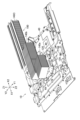
[1-1.回路基板ユニットの構成]
図1Aは、回路基板ユニット10の表側を示す斜視図である。図1Bは、回路基板ユニット10の裏側を示す底面図である。図2は、回路基板ユニット10の構成要素を示す分解斜視図である。 [1-1. Configuration of circuit board unit]
FIG. 1A is a perspective view showing the front side of thecircuit board unit 10. FIG. 1B is a bottom view showing the back side of the circuit board unit 10. FIG. 2 is an exploded perspective view showing the components of the circuit board unit 10.
図1Aは、回路基板ユニット10の表側を示す斜視図である。図1Bは、回路基板ユニット10の裏側を示す底面図である。図2は、回路基板ユニット10の構成要素を示す分解斜視図である。 [1-1. Configuration of circuit board unit]
FIG. 1A is a perspective view showing the front side of the
以下の説明では、図1Aなどに示すZ軸のZ1方向及びZ2方向を、それぞれ上方及び下方と称する。また、Z軸に対して垂直なY軸のY1方向及びY2方向を、それぞれ前方及び後方と称する。また、Z軸及びY軸に対して垂直なX軸のX1方向及びX2方向を、それぞれ左方向及び右方向と称する。ただし、これらの方向は、回路基板ユニット10の部品、部材、及び部分などの要素の形状や相対的な位置関係を説明するため規定されるものであり、電子機器における回路基板ユニット10の姿勢を限定するものではない。
In the following description, the Z1 direction and Z2 direction of the Z axis shown in FIG. 1A etc. are referred to as upper and lower, respectively. Further, the Y1 direction and the Y2 direction of the Y axis perpendicular to the Z axis are referred to as the front and the rear, respectively. Further, the X1 direction and the X2 direction of the X axis perpendicular to the Z axis and the Y axis are referred to as the left direction and the right direction, respectively. However, these directions are defined to explain the shapes and relative positional relationships of elements such as parts, members, and sections of the circuit board unit 10, and are not intended to describe the orientation of the circuit board unit 10 in electronic equipment. It is not limited.
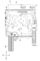
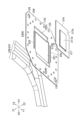
図2に示すように、回路基板ユニット10は、回路基板20と、回路基板シールド40と、放熱装置100とを有している。回路基板20は、上方(第1の方向、図2のZ1に示す方向)に向いている上面20U(図4を参照)と、下方(図2のZ2に示す方向)に向いている下面20Dを有している。図2に示すように、回路基板20の下面20Dには、複数のICチップ21a,21bが実装されている。また、回路基板20の上面20Uにも、ICチップ21c(図4を参照)などの複数の電子部品が実装されている。
As shown in FIG. 2, the circuit board unit 10 includes a circuit board 20, a circuit board shield 40, and a heat dissipation device 100. The circuit board 20 has an upper surface 20U (see FIG. 4) facing upward (a first direction, the direction indicated by Z1 in FIG. 2), and a lower surface 20D facing downward (the direction indicated by Z2 in FIG. 2). have. As shown in FIG. 2, a plurality of IC chips 21a and 21b are mounted on the lower surface 20D of the circuit board 20. Further, a plurality of electronic components such as an IC chip 21c (see FIG. 4) are also mounted on the upper surface 20U of the circuit board 20.
一例として、複数のICチップ21a,21bは、ROM(Read Only Memory)やRAM(Random Access Memory)などのメモリであり、ICチップ21cは、CPUやメモリなどを統合したSoCであるが、ICチップ21a,21b,21cの種類は、これに限定されない。ICチップ21a,21b,21cの少なくとも1つは、例えば、GPU(Graphics Processing Unit)であってもよい。図1B及び図2に示す例では、平面視において、1つのICチップ21cを複数のICチップ21a,21bが取り囲んでいる。複数のICチップ21aは、ICチップ21cの前側を囲み、複数のICチップ21bは、ICチップ21cの後側を囲んでいる。
As an example, the plurality of IC chips 21a and 21b are memories such as ROM (Read Only Memory) and RAM (Random Access Memory), and the IC chip 21c is an SoC that integrates a CPU, memory, etc. The types of 21a, 21b, and 21c are not limited to these. At least one of the IC chips 21a, 21b, and 21c may be, for example, a GPU (Graphics Processing Unit). In the example shown in FIGS. 1B and 2, one IC chip 21c is surrounded by a plurality of IC chips 21a and 21b in plan view. The plurality of IC chips 21a surround the front side of the IC chip 21c, and the plurality of IC chips 21b surround the rear side of the IC chip 21c.
回路基板シールド40は、導電性の材料によって形成され、例えば、鉄やアルミニウムなどの金属板に絞り加工などの板金加工を施すことで製造できる。回路基板シールド40は、複数の螺子やリベットなどにより回路基板20に固定される。回路基板シールド40は、回路基板20の上面20Uを覆っている。また、回路基板シールド40の外周部は、回路基板20のグラウンドパターンに接したり、回路基板20を挟んで回路基板シールド40とは反対側に配置されるシールドに接している。そして、回路基板シールド40の外周部は、回路基板20の上面20Uに実装されている複数の電子部品や配線を取り囲んでいる。これにより、回路基板20の上面20Uに実装されている複数の電子部品や配線などから発生するノイズ(不要輻射ノイズ)が回路基板ユニット10の外部に漏れることを抑制している。
The circuit board shield 40 is formed of a conductive material, and can be manufactured, for example, by performing sheet metal processing such as drawing on a metal plate such as iron or aluminum. The circuit board shield 40 is fixed to the circuit board 20 with a plurality of screws, rivets, or the like. The circuit board shield 40 covers the upper surface 20U of the circuit board 20. Further, the outer peripheral portion of the circuit board shield 40 is in contact with the ground pattern of the circuit board 20 or with a shield disposed on the opposite side of the circuit board shield 40 with the circuit board 20 interposed therebetween. The outer peripheral portion of the circuit board shield 40 surrounds a plurality of electronic components and wiring mounted on the upper surface 20U of the circuit board 20. This suppresses noise (unnecessary radiation noise) generated from a plurality of electronic components, wiring, etc. mounted on the upper surface 20U of the circuit board 20 from leaking to the outside of the circuit board unit 10.
図2に示すように、回路基板シールド40には、ICチップ21cの位置に、ICチップ21cを露出させる開口41が形成されている。この開口41の位置に、ICチップ21cを冷却するための放熱装置100が取り付けられている。放熱装置100は、回路基板シールド40に取り付けられ、回路基板シールド40に対して上方(図2のZ1に示す方向)に配置される。
As shown in FIG. 2, an opening 41 is formed in the circuit board shield 40 at the position of the IC chip 21c to expose the IC chip 21c. A heat dissipation device 100 for cooling the IC chip 21c is attached at the position of this opening 41. The heat dissipation device 100 is attached to the circuit board shield 40 and is arranged above the circuit board shield 40 (in the direction indicated by Z1 in FIG. 2).
[1-2.放熱装置の構成]
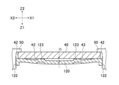
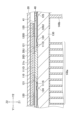
図1A及び図2に示すように、放熱装置100は、受熱ブロック110(図3及び図4を参照)と、ベースプレート120と、複数のヒートパイプ130(図1Aに示す例では6つのヒートパイプ130)と、ヒートシンク140a,140b,140cを有している。受熱ブロック110、複数のヒートパイプ130、及びヒートシンク140a,140b,140cは金属で形成され、SoCなどであるICチップ21cを冷却する。これらは、熱伝導率の高い金属(例えば、アルミニウムや、銅など)で形成されてよく、鉄で形成されてもよい。 [1-2. Configuration of heat dissipation device]
As shown in FIGS. 1A and 2, theheat dissipation device 100 includes a heat receiving block 110 (see FIGS. 3 and 4), a base plate 120, and a plurality of heat pipes 130 (six heat pipes 130 in the example shown in FIG. 1A). ) and heat sinks 140a, 140b, and 140c. The heat receiving block 110, the plurality of heat pipes 130, and the heat sinks 140a, 140b, and 140c are made of metal, and cool the IC chip 21c, which is an SoC or the like. These may be made of a metal with high thermal conductivity (eg, aluminum, copper, etc.), or may be made of iron.
図1A及び図2に示すように、放熱装置100は、受熱ブロック110(図3及び図4を参照)と、ベースプレート120と、複数のヒートパイプ130(図1Aに示す例では6つのヒートパイプ130)と、ヒートシンク140a,140b,140cを有している。受熱ブロック110、複数のヒートパイプ130、及びヒートシンク140a,140b,140cは金属で形成され、SoCなどであるICチップ21cを冷却する。これらは、熱伝導率の高い金属(例えば、アルミニウムや、銅など)で形成されてよく、鉄で形成されてもよい。 [1-2. Configuration of heat dissipation device]
As shown in FIGS. 1A and 2, the
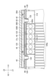
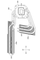
図3は、放熱装置100の底面図である。図4は、図3のIV-IV線を含む切断面における回路基板ユニット10の断面図である。図3及び図4に示すように、受熱ブロック110は、回路基板シールド40に形成されている開口41に対応した位置に設けられ、SoCなどであるICチップ21cに接している受熱面111Dを有している。受熱面111DとICチップ21cとの間には、グリスや液体金属など、熱伝導性材料が形成されてもよい。図4に示すように、受熱ブロック110には、階段状に下方(図4のZ2方向)に突出する凸部111が形成されている。この凸部111の頂部が、ICチップ21cの受熱面111Dと接触する。また、受熱ブロック110は、凸部111の位置から左側(X1側)と右側(X2側)とに延びている被固定部112を有している。後述するように、被固定部112はベースプレート120に固定される。被固定部112は、ヒートパイプ130が延伸する方向に交差する方向に延びている。
FIG. 3 is a bottom view of the heat dissipation device 100. FIG. 4 is a cross-sectional view of the circuit board unit 10 taken along the line IV--IV in FIG. As shown in FIGS. 3 and 4, the heat receiving block 110 is provided at a position corresponding to the opening 41 formed in the circuit board shield 40, and has a heat receiving surface 111D that is in contact with an IC chip 21c such as an SoC. are doing. A thermally conductive material such as grease or liquid metal may be formed between the heat receiving surface 111D and the IC chip 21c. As shown in FIG. 4, the heat receiving block 110 is formed with a convex portion 111 that protrudes downward (Z2 direction in FIG. 4) in a stepwise manner. The top of this convex portion 111 contacts the heat receiving surface 111D of the IC chip 21c. Further, the heat receiving block 110 has a fixed portion 112 extending from the position of the convex portion 111 to the left side (X1 side) and the right side (X2 side). As will be described later, the fixed portion 112 is fixed to the base plate 120. The fixed portion 112 extends in a direction intersecting the direction in which the heat pipe 130 extends.
ベースプレート120は導電性の材料によって形成される。例えば、ベースプレート120は、鉄やアルミニウムなどの金属板により形成されている。ベースプレート120は、回路基板シールド40に取り付けられる。図3及び図4に示すように、ベースプレート120は、ICチップ21cに対応する位置に開口121を有している。ベースプレート120には、受熱ブロック110が半田などの固定手段によって固定されており、ベースプレート120の開口121から、受熱ブロック110の受熱面111Dが露出している。回路基板シールド40の開口41ではICチップ21cが露出している。図4に示すように、回路基板シールド40の開口41にベースプレート120の開口121が配置されることにより、受熱ブロック110の受熱面111DがICチップ21cに接触する。ベースプレート120の下面120D(図4を参照、図4では上側を向いた面)には、受熱面111Dを取り囲み、受熱面111DとICチップ21cとの間に塗布される熱伝導性材料の広がりを抑えるシートやスポンジなどが貼り付けられてもよい。
The base plate 120 is made of a conductive material. For example, the base plate 120 is formed of a metal plate such as iron or aluminum. Base plate 120 is attached to circuit board shield 40 . As shown in FIGS. 3 and 4, the base plate 120 has an opening 121 at a position corresponding to the IC chip 21c. The heat receiving block 110 is fixed to the base plate 120 by fixing means such as solder, and the heat receiving surface 111D of the heat receiving block 110 is exposed through the opening 121 of the base plate 120. The IC chip 21c is exposed in the opening 41 of the circuit board shield 40. As shown in FIG. 4, the opening 121 of the base plate 120 is arranged in the opening 41 of the circuit board shield 40, so that the heat receiving surface 111D of the heat receiving block 110 comes into contact with the IC chip 21c. The lower surface 120D (see FIG. 4, the surface facing upward in FIG. 4) of the base plate 120 has a spread of thermally conductive material surrounding the heat receiving surface 111D and applied between the heat receiving surface 111D and the IC chip 21c. A suppressing sheet, sponge, etc. may be attached.
図3に示すように、ベースプレート120にはガイド穴129が成形されている。また、図1Aに示すように、回路基板シールド40には上方に突出するガイド凸部49が形成されている。回路基板シールド40のガイド凸部がベースプレート120のガイド穴129を通ることにより、回路基板シールド40におけるベースプレート120の位置決めを容易にできる。
As shown in FIG. 3, a guide hole 129 is formed in the base plate 120. Further, as shown in FIG. 1A, the circuit board shield 40 is formed with a guide convex portion 49 that projects upward. Since the guide convex portion of the circuit board shield 40 passes through the guide hole 129 of the base plate 120, the base plate 120 can be easily positioned on the circuit board shield 40.
図2及び図3に示すように、複数のヒートパイプ130及びヒートシンク140a,140b,140cは、ベースプレート120の一方の面を覆うように、ベースプレート120の上方(Z1方向、図2では下方)に位置している。受熱面111Dが設けられている受熱ブロック110は、複数のヒートパイプ130と接続し、ICチップ21cの熱をヒートパイプ130に伝える。ヒートパイプ130は、受熱ブロック110から受けたICチップ21cの熱をヒートシンク140a,140b,140cの少なくとも1つに伝える。ヒートシンク140a,140b,140cは、複数のヒートパイプ130のうちの少なくとも1つと接続し、ヒートパイプ130を介して伝わったICチップ21cの熱を放出する。図1Aに示すように、放熱装置100が回路基板シールド40に取り付けられている状態で、ヒートシンク140a,140b,140cは、回路基板シールド40の上方に位置する複数のフィンを有している。複数のフィンは、例えば、左右方向に並んでいる。ヒートシンク140aは、ベースプレート120の上方に位置し、ベースプレート120に形成されている開口121を覆っている。
As shown in FIGS. 2 and 3, the plurality of heat pipes 130 and heat sinks 140a, 140b, 140c are positioned above the base plate 120 (in the Z1 direction, downward in FIG. 2) so as to cover one surface of the base plate 120. are doing. The heat receiving block 110 provided with the heat receiving surface 111D is connected to a plurality of heat pipes 130 and transmits the heat of the IC chip 21c to the heat pipes 130. The heat pipe 130 transfers the heat of the IC chip 21c received from the heat receiving block 110 to at least one of the heat sinks 140a, 140b, and 140c. The heat sinks 140a, 140b, and 140c are connected to at least one of the plurality of heat pipes 130, and emit heat from the IC chip 21c transmitted via the heat pipe 130. As shown in FIG. 1A, when the heat dissipation device 100 is attached to the circuit board shield 40, the heat sinks 140a, 140b, 140c have a plurality of fins located above the circuit board shield 40. For example, the plurality of fins are arranged in the left-right direction. The heat sink 140a is located above the base plate 120 and covers the opening 121 formed in the base plate 120.
図4に示すように、複数のヒートパイプ130は連結部131を有しており、左右方向において隣り合う2つのヒートパイプ130は、連結部131において相互に連結されている。ヒートパイプ130の連結部131は、受熱ブロック110の上面110Uに設けられた凹部113の内側に収容されて、上下方向において、受熱ブロック110とヒートシンク140aの間に配置されている。
As shown in FIG. 4, the plurality of heat pipes 130 have a connecting portion 131, and two heat pipes 130 adjacent in the left-right direction are connected to each other at the connecting portion 131. The connecting portion 131 of the heat pipe 130 is accommodated inside the recess 113 provided in the upper surface 110U of the heat receiving block 110, and is arranged between the heat receiving block 110 and the heat sink 140a in the vertical direction.
[1-3.回路基板シールドの開口におけるノイズ対策]
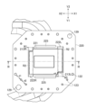
図2に示すように、回路基板シールド40は、複数の取付穴42を有している。複数の取付穴42は、回路基板シールド40の開口41を取り囲むように配置されている。また、図2及び図3に示すように、放熱装置100のベースプレート120も、複数の取付穴122を有している。複数の取付穴122は、ベースプレート120の開口121を取り囲むように配置されている。図3において、開口121を取り囲む複数の二重丸は、いずれも取付穴122を示している。回路基板シールド40に放熱装置100が取り付けられている状態で、回路基板シールド40に形成されている取付穴42の位置と、ベースプレート120に形成さている取付穴122の位置は一致している。 [1-3. Noise countermeasures for openings in circuit board shields]
As shown in FIG. 2,circuit board shield 40 has a plurality of mounting holes 42. As shown in FIG. The plurality of mounting holes 42 are arranged to surround the opening 41 of the circuit board shield 40. Further, as shown in FIGS. 2 and 3, the base plate 120 of the heat dissipation device 100 also has a plurality of attachment holes 122. The plurality of attachment holes 122 are arranged so as to surround the opening 121 of the base plate 120. In FIG. 3, a plurality of double circles surrounding the opening 121 all indicate attachment holes 122. When the heat dissipation device 100 is attached to the circuit board shield 40, the position of the mounting hole 42 formed in the circuit board shield 40 and the position of the mounting hole 122 formed in the base plate 120 match.
図2に示すように、回路基板シールド40は、複数の取付穴42を有している。複数の取付穴42は、回路基板シールド40の開口41を取り囲むように配置されている。また、図2及び図3に示すように、放熱装置100のベースプレート120も、複数の取付穴122を有している。複数の取付穴122は、ベースプレート120の開口121を取り囲むように配置されている。図3において、開口121を取り囲む複数の二重丸は、いずれも取付穴122を示している。回路基板シールド40に放熱装置100が取り付けられている状態で、回路基板シールド40に形成されている取付穴42の位置と、ベースプレート120に形成さている取付穴122の位置は一致している。 [1-3. Noise countermeasures for openings in circuit board shields]
As shown in FIG. 2,
図5は、図3のV-V線を含む切断面における回路基板ユニット10の断面図である。放熱装置100は、ICチップ21cを取り囲むように配置されている複数の取付穴42,122(固定部)で回路基板シールド40に固定されている。図5に示すように、回路基板シールド40に形成されている取付穴42と、放熱装置100のベースプレート120に形成されている取付穴122は、螺子やリベットなどの1つの固定具50が通されることによって締結されている。このように、回路基板シールド40に放熱装置100のベースプレート120を固定することにより、取付穴42,122の位置において回路基板シールド40とベースプレート120との接触の安定性が確保され、回路基板20上で発生したノイズが、回路基板シールド40の開口41と、回路基板シールド40とベースプレート120との間に生じる隙間とを通過して、回路基板シールド40の外部に漏れることを抑制できる。つまり、放熱装置100を取り付ける構造自体がノイズ対策のシールド構造を兼ねている。
FIG. 5 is a cross-sectional view of the circuit board unit 10 taken along the line VV in FIG. 3. The heat dissipation device 100 is fixed to the circuit board shield 40 through a plurality of mounting holes 42, 122 (fixing portions) arranged so as to surround the IC chip 21c. As shown in FIG. 5, the mounting hole 42 formed in the circuit board shield 40 and the mounting hole 122 formed in the base plate 120 of the heat dissipation device 100 allow a fixing device 50 such as a screw or a rivet to pass through. It is concluded by In this way, by fixing the base plate 120 of the heat dissipation device 100 to the circuit board shield 40, the stability of the contact between the circuit board shield 40 and the base plate 120 at the positions of the mounting holes 42, 122 is ensured, and the stability of the contact between the circuit board shield 40 and the base plate 120 is secured. The noise generated can be prevented from leaking to the outside of the circuit board shield 40 through the opening 41 of the circuit board shield 40 and the gap created between the circuit board shield 40 and the base plate 120. In other words, the structure itself to which the heat dissipation device 100 is attached also serves as a shield structure for noise countermeasures.
回路基板シールド40とベースプレート120のいずれか一方は、他方側に向けて突出している接触凸部123を有する。接触凸部123は、回路基板シールド40とベースプレート120の対向する部分に形成される。図3及び図5に示す例では、ベースプレート120が、回路基板シールド40に対向する面に回路基板シールド40側に向けて突出している(図5においては、下方(Z2方向)に突出している)複数の接触凸部123(第1接触凸部)を有している。図3において、開口121を取り囲むハッチングを施した複数の丸は、いずれも接触凸部123を示している。接触凸部123は、ベースプレート120に板金加工を施すことで形成されている。このように板金加工で形成することで、ベースプレート120における接触凸部123の形成が容易になる。
Either the circuit board shield 40 or the base plate 120 has a contact protrusion 123 that protrudes toward the other side. The contact convex portion 123 is formed on a portion of the circuit board shield 40 and the base plate 120 that face each other. In the examples shown in FIGS. 3 and 5, the base plate 120 protrudes toward the circuit board shield 40 on the surface facing the circuit board shield 40 (in FIG. 5, it protrudes downward (in the Z2 direction)). It has a plurality of contact protrusions 123 (first contact protrusions). In FIG. 3 , a plurality of hatched circles surrounding the opening 121 all indicate the contact convex portion 123 . The contact convex portion 123 is formed by subjecting the base plate 120 to sheet metal processing. Forming by sheet metal processing in this manner facilitates the formation of the contact protrusion 123 on the base plate 120.
接触凸部123が板金加工によって形成される場合、接触凸部123はベースプレート120の下面120D(Z2側に向いた面、図5において上側に向いた面)に形成される一方で、ベースプレート120の上面120∪(Z1側に向いた面、図5において下側に向いた面)は、接触凸部123の位置に凹部を有してよい。なお、接触凸部123は板金加工によって形成される部分でなくてもよい。例えば、ベースプレート120は、接触凸部123として、半田によって形成された凸部を有してもよい。
When the contact convex portion 123 is formed by sheet metal processing, the contact convex portion 123 is formed on the lower surface 120D of the base plate 120 (the surface facing the Z2 side, the surface facing upward in FIG. 5); The upper surface 120∪ (the surface facing the Z1 side, the surface facing downward in FIG. 5) may have a recess at the position of the contact convex portion 123. Note that the contact convex portion 123 does not have to be formed by sheet metal processing. For example, the base plate 120 may have a protrusion formed of solder as the contact protrusion 123.
図5に示すように、回路基板シールド40は、ベースプレート120の接触凸部123と接触している接触部43を有している。このように、ベースプレート120に接触凸部123を形成し、接触部43の位置において、回路基板シールド40とベースプレート120とが接触することにより、回路基板20上で発生したノイズが、回路基板シールド40の開口41と、回路基板シールド40とベースプレート120との間に生じる隙間とを通過して、回路基板シールド40の外部に漏れることを抑制できる。
As shown in FIG. 5, the circuit board shield 40 has a contact portion 43 that is in contact with the contact protrusion 123 of the base plate 120. In this way, by forming the contact convex portion 123 on the base plate 120 and making contact between the circuit board shield 40 and the base plate 120 at the position of the contact portion 43, noise generated on the circuit board 20 is transferred to the circuit board shield 40. It is possible to suppress leakage to the outside of the circuit board shield 40 through the opening 41 and the gap created between the circuit board shield 40 and the base plate 120.
図3に示すように、放熱装置100のベースプレート120において、複数の接触凸部123は、複数の取付穴122とともに開口121(ICチップ21c)を取り囲むように配置されている。ベースプレート120において、複数の取付穴122のうち、隣り合う2つの取付穴122の間に、少なくとも1つの接触凸部123が形成されている。そして、ベースプレート120と、回路基板シールド40は、複数の取付穴42,122及び複数の接触凸部123を介して互いに接触している。このように、ICチップ21cを取り囲む複数の位置でベースプレート120と回路基板シールド40とが接触しているため、回路基板20上で発生したノイズが、回路基板シールド40の開口41と、回路基板シールド40とベースプレート120との間に生じる隙間とを通過して、回路基板シールド40の外部(回路基板シールド40と回路基板20との間の空間の外部)に漏れることを効果的に抑制できる。
As shown in FIG. 3, in the base plate 120 of the heat dissipation device 100, the plurality of contact protrusions 123 are arranged to surround the opening 121 (IC chip 21c) together with the plurality of mounting holes 122. In the base plate 120, at least one contact protrusion 123 is formed between two adjacent mounting holes 122 among the plurality of mounting holes 122. The base plate 120 and the circuit board shield 40 are in contact with each other via the plurality of mounting holes 42 , 122 and the plurality of contact protrusions 123 . As described above, since the base plate 120 and the circuit board shield 40 are in contact with each other at multiple positions surrounding the IC chip 21c, noise generated on the circuit board 20 is transmitted to the opening 41 of the circuit board shield 40 and the circuit board shield. 40 and the base plate 120 and leakage to the outside of the circuit board shield 40 (outside the space between the circuit board shield 40 and the circuit board 20) can be effectively suppressed.
図6は、ベースプレート120において、取付穴122と接触凸部123とが並んでいる方向に沿った切断面で得られる回路基板ユニット10の模式的な断面図である。図6に示すように、ベースプレート120は、取付穴42の位置で回路基板シールド40に固定され、接触凸部123が接触部43に接触することにより、回路基板シールド40に対して撓む。このような撓みを生じさせるため、ベースプレート120は、回路基板シールド40よりも低い剛性を有してよい。ベースプレート120は、例えば、上下方向における厚さが回路基板シールド40より小さい部材であってよい。また、ベースプレート120は、回路基板シールド40の材料とは異なる材料であってもよい。ベースプレート120は、回路基板シールド40よりも軟らかい材料によって形成されてもよい。例えば、回路基板シールド40及びベースプレート120を同素材の鉄で構成し、それぞれ板厚の異なる板金を用いて形成されてもよい。その場合、ベースプレート120の板厚は回路基板シールド40の板厚よりも小さいと好ましい。また、回路基板シールド40及びベースプレート120は異素材で形成されてもよい。例えば、回路基板シールド40は鉄で形成され、ベースプレート120はアルミニウムで形成されてもよい。
FIG. 6 is a schematic cross-sectional view of the circuit board unit 10 taken along the direction in which the mounting holes 122 and the contact protrusions 123 are lined up in the base plate 120. As shown in FIG. 6, the base plate 120 is fixed to the circuit board shield 40 at the position of the mounting hole 42, and is bent with respect to the circuit board shield 40 when the contact convex portion 123 contacts the contact portion 43. To accommodate this deflection, base plate 120 may have a lower stiffness than circuit board shield 40. The base plate 120 may be a member having a thickness smaller in the vertical direction than the circuit board shield 40, for example. Additionally, the base plate 120 may be made of a different material than the material of the circuit board shield 40. Base plate 120 may be formed of a softer material than circuit board shield 40. For example, the circuit board shield 40 and the base plate 120 may be made of the same material of iron, and may be formed using sheet metals having different thicknesses. In that case, the thickness of the base plate 120 is preferably smaller than the thickness of the circuit board shield 40. Further, the circuit board shield 40 and the base plate 120 may be formed of different materials. For example, circuit board shield 40 may be formed of iron and base plate 120 may be formed of aluminum.
図6に示すように、ベースプレート120が回路基板シールド40に対して撓むことにより、2つの接触凸部123の間に隙間Cが形成される場合がある。ここで、ベースプレート120において、2つの取付穴122の間に形成される接触凸部123の数を3つにすると、これらの3つの接触凸部123のうちの真ん中の接触凸部123は、隙間Cの付近に配置される可能性がある。このため、ベースプレート120において、2つの取付穴122の間に配置される接触凸部123の数は、2つ以下とすることが望ましい。換言すると、回路基板シールド40において、2つの取付穴42の間に設けられる接触部43数は、2つ以下とすることが望ましい。このようにすることで、ベースプレート120と回路基板シールド40との接触の安定性が十分に確保され、回路基板20上で発生したノイズの遮断性能を向上できる。
As shown in FIG. 6, when the base plate 120 is bent with respect to the circuit board shield 40, a gap C may be formed between the two contact protrusions 123. Here, in the base plate 120, if the number of contact protrusions 123 formed between the two mounting holes 122 is three, the middle contact protrusion 123 among these three contact protrusions 123 will fill the gap. There is a possibility that it will be placed near C. For this reason, in the base plate 120, it is desirable that the number of contact protrusions 123 arranged between the two mounting holes 122 be two or less. In other words, in the circuit board shield 40, the number of contact portions 43 provided between the two mounting holes 42 is preferably two or less. By doing so, the stability of the contact between the base plate 120 and the circuit board shield 40 is sufficiently ensured, and the performance of blocking noise generated on the circuit board 20 can be improved.
ベースプレート120の取付穴122及び接触凸部123(回路基板シールド40の取付穴42及び接触部43)は、放熱装置100と回路基板シールド40との接点である。ここで、隣り合う2つの接点の距離(取付穴122と接触凸部123との距離d1(図3参照)、及び2つの接触凸部123の距離d2(図3参照))は、回路基板シールド40で遮蔽したいノイズの波長に基づいて決定することが望ましい。例えば、隣り合う2つの接点の距離は、いずれも、回路基板シールド40が遮蔽するノイズの波長の3分の1未満、より好ましくは、波長の4分の1未満に設定されてよい。また、隣り合う2つの接点の距離は、いずれも20mmであることが好ましい。これにより、無線通信などで使用される周波数帯のノイズの漏洩を効果的に抑制できる。隣り合う2つの接点の距離は、いずれも15mm以下であることが好ましい。隣り合う2つの接点の距離は、いずれも10mm以下であることが更に好ましい。
The mounting hole 122 and the contact convex portion 123 of the base plate 120 (the mounting hole 42 and the contact portion 43 of the circuit board shield 40) are the contact points between the heat dissipation device 100 and the circuit board shield 40. Here, the distance between two adjacent contacts (the distance d1 between the mounting hole 122 and the contact protrusion 123 (see Figure 3), and the distance d2 between the two contact protrusions 123 (see Figure 3)) is It is preferable to make the decision based on the wavelength of the noise that you want to block at 40. For example, the distance between two adjacent contacts may be set to be less than one-third of the wavelength of the noise that the circuit board shield 40 shields, and more preferably less than one-fourth of the wavelength of the noise that is shielded by the circuit board shield 40. Further, the distance between two adjacent contact points is preferably 20 mm. Thereby, it is possible to effectively suppress leakage of noise in the frequency band used in wireless communication and the like. The distance between two adjacent contact points is preferably 15 mm or less. More preferably, the distance between two adjacent contact points is 10 mm or less.
[1-4.シールドプレートの開口におけるノイズ対策]
回路基板シールド40の開口41の位置に、ベースプレート120の開口121が形成されている。図3及び図4に示すように、ベースプレート120の開口121は、ベースプレート120に取り付けられる受熱ブロック110によって塞がれている。図4に示すように、受熱ブロック110は、階段状に突出する凸部111を有している。受熱ブロック110の凸部111は、ベースプレート120の開口121を通過し、凸部111の外周縁111Sは、開口121の縁と接している。このようにすることで、ベースプレート120の開口121からノイズが漏れることを抑制できる。 [1-4. Noise countermeasures at the opening of the shield plate]
Anopening 121 in the base plate 120 is formed at the position of the opening 41 in the circuit board shield 40 . As shown in FIGS. 3 and 4, the opening 121 of the base plate 120 is closed by the heat receiving block 110 attached to the base plate 120. As shown in FIG. 4, the heat receiving block 110 has a convex portion 111 that protrudes stepwise. The protrusion 111 of the heat receiving block 110 passes through the opening 121 of the base plate 120, and the outer peripheral edge 111S of the protrusion 111 is in contact with the edge of the opening 121. By doing so, it is possible to suppress noise from leaking from the opening 121 of the base plate 120.
回路基板シールド40の開口41の位置に、ベースプレート120の開口121が形成されている。図3及び図4に示すように、ベースプレート120の開口121は、ベースプレート120に取り付けられる受熱ブロック110によって塞がれている。図4に示すように、受熱ブロック110は、階段状に突出する凸部111を有している。受熱ブロック110の凸部111は、ベースプレート120の開口121を通過し、凸部111の外周縁111Sは、開口121の縁と接している。このようにすることで、ベースプレート120の開口121からノイズが漏れることを抑制できる。 [1-4. Noise countermeasures at the opening of the shield plate]
An
ベースプレート120は、開口121を取り囲むシールド構造を有している。シールド構造は、ICチップ21cの熱を伝える受熱ブロック110又はヒートパイプ130と、ベースプレート120との間に形成されている。このシールド構造によると、回路基板20上で発生したノイズが、回路基板シールド40の開口41と、ベースプレート120の開口121と、ベースプレート120と受熱ブロック110との間に生じる隙間(又はベースプレート120とヒートパイプ130との間に生じる隙間)とを通過して、回路基板シールド40の外部に漏れることを効果的に抑制できる。シールド構造は、矩形の開口121の縁の向きに応じて異なる構成を有してもよい。ヒートパイプ130の連結部131においてヒートパイプ130が延伸する方向に沿った開口121の縁(前後方向に沿った縁)と、その縁と交差する方向に沿った開口121の縁(左右方向に沿った縁)とで異なる構造を有してもよい。
The base plate 120 has a shield structure surrounding the opening 121. The shield structure is formed between the base plate 120 and the heat receiving block 110 or heat pipe 130 that transfers the heat of the IC chip 21c. According to this shield structure, noise generated on the circuit board 20 is transmitted through the opening 41 of the circuit board shield 40, the opening 121 of the base plate 120, and the gap between the base plate 120 and the heat receiving block 110 (or the gap between the base plate 120 and the heat receiving block 110). It is possible to effectively suppress leakage to the outside of the circuit board shield 40 through the gap between the pipe 130 and the pipe 130 . The shield structure may have different configurations depending on the orientation of the edges of the rectangular opening 121. In the connecting portion 131 of the heat pipe 130, the edge of the opening 121 along the direction in which the heat pipe 130 extends (the edge along the front-rear direction), and the edge of the opening 121 along the direction intersecting the edge (along the left-right direction). The two edges may have different structures.
図3及び図4に示すように、放熱装置100は、ベースプレート120の開口121を取り囲うシールド構造として、例えば、ベースプレート120と受熱ブロック110とが相互に固定される固定領域R1を有している。固定領域R1の一部は、例えば、受熱ブロック110の被固定部112に設けられる。被固定部112は、受熱ブロック110の凸部111の位置から、ヒートパイプ130の連結部131におけるヒートパイプ130の延伸方向とは交差する方向(右方向及び左方向)において延びており、且つ、ヒートパイプ130の延伸方向(前後方向)に延びている。固定領域R1は、ベースプレート120の開口121の対向する2辺のそれぞれに沿って設けられている。ベースプレート120及び受熱ブロック110の被固定部112は、固定領域R1において、半田などの固定手段により相互に固定されている。図4に示すように、受熱ブロック110の被固定部112は、ベースプレート120の上面120U(図4では下側の面)に固定されてよい。この場合、半田は被固定部112の下面(図4において、Z2側に向いた面)の全域に塗布されてよい。このように、開口121に対して、連結部131におけるヒートパイプ130の延伸方向とは交差する方向(右方向及び左方向)の位置において、ベースプレート120及び受熱ブロック110が固定手段を介して接触することにより、回路基板20上で生じたノイズが、ベースプレート120と受熱ブロック110との間に生じる隙間を通過して、回路基板シールド40の外部に漏れることを効果的に抑制できる。
As shown in FIGS. 3 and 4, the heat dissipation device 100 has a fixing region R1 where the base plate 120 and the heat receiving block 110 are fixed to each other, for example, as a shield structure surrounding the opening 121 of the base plate 120. . A part of the fixing region R1 is provided, for example, in the fixed portion 112 of the heat receiving block 110. The fixed portion 112 extends from the position of the convex portion 111 of the heat receiving block 110 in a direction (rightward and leftward) that intersects the extending direction of the heat pipe 130 at the connecting portion 131 of the heat pipe 130, and It extends in the extending direction of the heat pipe 130 (front-back direction). The fixed region R1 is provided along each of two opposing sides of the opening 121 of the base plate 120. The base plate 120 and the fixed portion 112 of the heat receiving block 110 are fixed to each other in the fixing region R1 by fixing means such as solder. As shown in FIG. 4, the fixed portion 112 of the heat receiving block 110 may be fixed to the upper surface 120U (lower surface in FIG. 4) of the base plate 120. In this case, the solder may be applied to the entire lower surface of the fixed portion 112 (the surface facing the Z2 side in FIG. 4). In this way, the base plate 120 and the heat receiving block 110 come into contact with each other via the fixing means at the positions of the connecting portion 131 in the direction (rightward and leftward) that intersects the extending direction of the heat pipe 130 with respect to the opening 121. As a result, noise generated on the circuit board 20 can be effectively prevented from leaking to the outside of the circuit board shield 40 through the gap created between the base plate 120 and the heat receiving block 110.
図7は、図3のVII-VII線を含む切断面における回路基板ユニット10の断面図である。図3及び図7に示すように、ベースプレート120は、開口121を取り囲うシールド構造として、他にも例えば、ヒートパイプ130側に突出している(図7では、上方(Z1の方向)に突出している)接触凸部124(第2接触凸部)を有している。接触凸部124は、開口121に対して、ヒートパイプ130の連結部131におけるヒートパイプ130の延伸方向(前方及び後方)の位置に形成されている。図3に示すように、接触凸部124は、開口121の対向する2辺に沿って設けられており、左右方向に延びている。ベースプレート120と、ICチップ21cの熱を伝えるヒートパイプ130は、接触凸部124を介して互いに接触している。このように、開口121に対して、連結部131におけるヒートパイプ130の延伸方向(前方及び後方)の位置において、ベースプレート120及びヒートパイプ130が接触凸部124を介して接触することにより、回路基板20上で生じたノイズが、ベースプレート120とヒートパイプ130との間に生じる隙間を通過して、回路基板シールド40の外部に漏れることを効果的に抑制できる。
FIG. 7 is a cross-sectional view of the circuit board unit 10 taken along the line VII-VII in FIG. 3. As shown in FIGS. 3 and 7, the base plate 120 has a shield structure that surrounds the opening 121, and also projects toward the heat pipe 130 (in FIG. 7, it projects upward (in the Z1 direction)). It has a contact protrusion 124 (second contact protrusion). The contact convex portion 124 is formed at a position in the connecting portion 131 of the heat pipe 130 in the extending direction (front and rear) of the heat pipe 130 with respect to the opening 121 . As shown in FIG. 3, the contact protrusions 124 are provided along two opposing sides of the opening 121 and extend in the left-right direction. The base plate 120 and the heat pipe 130 that transfers the heat of the IC chip 21c are in contact with each other via the contact protrusion 124. In this way, the base plate 120 and the heat pipe 130 come into contact with the opening 121 via the contact convex part 124 at the position in the connecting part 131 in the extending direction (front and rear) of the heat pipe 130, thereby causing the circuit board Noise generated on the circuit board shield 20 can be effectively prevented from leaking to the outside of the circuit board shield 40 through the gap created between the base plate 120 and the heat pipe 130.
ヒートパイプ130は、半田などの固定手段によってベースプレート120の接触凸部124に固定されてもよい。これにより、接触凸部124の位置において、ベースプレート120とヒートパイプ130との接触の安定性が確保され、ベースプレート120とヒートパイプ130との間の隙間を通して回路基板20上で発生したノイズが回路基板シールド40の外部に漏れることを効果的に抑制できる。また、ベースプレート120は、図7で示すように、後側の接触凸部124の後方(Y2の方向)に、上方に突出する凸部125を有してよい。ヒートパイプ130は、半田などの固定手段によって凸部125に固定されてもよい。このようにすることで、ベースプレート120におけるヒートパイプ130の固定の安定性を確保できる。
The heat pipe 130 may be fixed to the contact protrusion 124 of the base plate 120 by a fixing means such as solder. As a result, the stability of the contact between the base plate 120 and the heat pipe 130 is ensured at the position of the contact protrusion 124, and the noise generated on the circuit board 20 passes through the gap between the base plate 120 and the heat pipe 130. Leakage to the outside of the shield 40 can be effectively suppressed. Further, as shown in FIG. 7, the base plate 120 may have a protrusion 125 that protrudes upward behind the contact protrusion 124 on the rear side (in the direction of Y2). The heat pipe 130 may be fixed to the protrusion 125 by a fixing means such as solder. By doing so, the stability of fixing the heat pipe 130 on the base plate 120 can be ensured.
図3に示すように、ベースプレート120の開口121に対し、ヒートパイプ130の連結部131におけるヒートパイプ130の延伸方向とは交差する方向(右方向及び左方向)の位置に設けられている固定領域R1は、ベースプレート120の上面120U(図4を参照、図4では下側の面)において、連結部131におけるヒートパイプ130の延伸方向(前後方向)に伸びている。また、ベースプレート120の開口121に対し、連結部131におけるヒートパイプ130の延伸方向(前方及び後方)の位置に設けられている接触凸部124は、ベースプレート120の上面120U(図7を参照、図7では下側の面)において、連結部131におけるヒートパイプ130の延伸方向とは交差する方向(右方向及び左方向)に伸びている。これにより、固定領域R1と接触凸部124とを含むシールド構造(固定領域R1及び接触凸部124)は、開口121を取り囲んでいる。これにより、回路基板20上で生じたノイズが、開口41,121、及び、回路基板シールド40とベースプレート120との間の隙間、ベースプレート120と受熱ブロック110との間の隙間、及びベースプレート120とヒートパイプ130との間の隙間)を通して、回路基板シールド40の外部に漏れることを抑制できる。つまり、放熱装置100全体が一体としてシールド構造を構成し、放熱装置100が回路基板シールド40に取り付けられることにより、回路基板シールド40の外部にノイズが漏れることを抑制できる。
As shown in FIG. 3, the fixing area is provided at a position in the connecting portion 131 of the heat pipe 130 in a direction (rightward and leftward) that intersects the extending direction of the heat pipe 130 with respect to the opening 121 of the base plate 120. R1 extends in the extending direction (front-back direction) of the heat pipe 130 in the connecting portion 131 on the upper surface 120U of the base plate 120 (see FIG. 4, the lower surface in FIG. 4). Further, the contact convex portion 124 provided in the connecting portion 131 in the extending direction (front and rear) of the heat pipe 130 with respect to the opening 121 of the base plate 120 is connected to the upper surface 120U of the base plate 120 (see FIG. 7, 7, the lower surface) extends in a direction (rightward and leftward) that intersects the extending direction of the heat pipe 130 in the connecting portion 131. As a result, the shield structure including the fixed region R1 and the contact convex portion 124 (fixed region R1 and the contact convex portion 124) surrounds the opening 121. As a result, the noise generated on the circuit board 20 is transmitted to the openings 41 and 121, the gap between the circuit board shield 40 and the base plate 120, the gap between the base plate 120 and the heat receiving block 110, and the gap between the base plate 120 and the heat receiving block 110. It is possible to suppress leakage to the outside of the circuit board shield 40 through the gap between the pipe 130 and the pipe 130. That is, the entire heat dissipation device 100 forms a shield structure as one piece, and by attaching the heat dissipation device 100 to the circuit board shield 40, it is possible to suppress leakage of noise to the outside of the circuit board shield 40.
受熱ブロック110の上面110Uには凹部113が形成されており、受熱ブロック110とベースプレート120との間に位置するヒートパイプ130の連結部131は、受熱ブロック110の凹部113の内側を通過するように前後方向に伸びている。このため、ヒートパイプ130の連結部131の延伸方向での位置に、ベースプレート120と受熱ブロック110とが直接接続する固定領域R1を設けることは難しい。そこで、ベースプレート120の開口121を取り囲むシールド構造は、開口121に対し、ヒートパイプ130の連結部131におけるヒートパイプ130の延伸方向(前方及び後方)の位置では、接触凸部124を介してヒートパイプ130に接している。一方で、開口121に対し、連結部131におけるヒートパイプ130の延伸方向とは交差する方向(右方向及び左方向)の位置では、固定領域R1を介して受熱ブロック110と接している。このように、開口121に対し、ヒートパイプ130の延伸方向での位置と、ヒートパイプ130の延伸方向とは交差する方向での位置とで、シールド構造が接する部材(ヒートパイプ130又は受熱ブロック110)を分けることによって、シールド構造は開口121を取り囲むことができる。これにより、回路基板シールド40の外部に漏れることを抑制できる。
A recess 113 is formed in the upper surface 110U of the heat receiving block 110, and the connecting portion 131 of the heat pipe 130 located between the heat receiving block 110 and the base plate 120 is configured to pass through the inside of the recess 113 of the heat receiving block 110. It extends in the front and back direction. Therefore, it is difficult to provide a fixed region R1 where the base plate 120 and the heat receiving block 110 are directly connected at a position in the extending direction of the connecting portion 131 of the heat pipe 130. Therefore, the shield structure that surrounds the opening 121 of the base plate 120 has a structure in which the heat pipe is connected to the opening 121 through the contact convex portion 124 at a position in the extending direction (front and rear) of the heat pipe 130 at the connecting portion 131 of the heat pipe 130. It is in contact with 130. On the other hand, with respect to the opening 121, the connecting portion 131 is in contact with the heat receiving block 110 via the fixing region R1 at positions in the direction (rightward and leftward) that intersect with the extending direction of the heat pipe 130. In this way, the members (heat pipes 130 or heat receiving blocks 110 ), the shield structure can surround the opening 121. Thereby, leakage to the outside of the circuit board shield 40 can be suppressed.
ベースプレート120に設けられている固定領域R1と接触凸部124との距離d3(図3を参照)は、ベースプレート120で遮蔽したいノイズの波長に基づいて決定することが望ましい。例えば、固定領域R1と接触凸部124との距離d3は、いずれも、ベースプレート120が遮蔽するノイズの波長の3分の1未満であるのが好ましい。距離d3は波長の4分の1未満に設定されるのが、更に好ましい。また、固定領域R1と接触凸部124との距離d3は、いずれも20mmであることが好ましい。これにより、無線通信などで使用される周波数帯のノイズの漏洩を効果的に抑制できる。距離d3は、いずれも15mm以下であることが好ましい。距離d3は、いずれも10mm以下であることが更に好ましい。
It is desirable that the distance d3 (see FIG. 3) between the fixed region R1 provided on the base plate 120 and the contact protrusion 124 be determined based on the wavelength of the noise that the base plate 120 wants to block. For example, it is preferable that the distance d3 between the fixed region R1 and the contact convex portion 124 is less than one third of the wavelength of noise that the base plate 120 blocks. More preferably, the distance d3 is set to less than one quarter of the wavelength. Moreover, it is preferable that the distance d3 between the fixed region R1 and the contact convex portion 124 is both 20 mm. Thereby, it is possible to effectively suppress leakage of noise in the frequency band used in wireless communication and the like. It is preferable that each distance d3 is 15 mm or less. It is further preferable that the distance d3 is 10 mm or less.
[1-5.まとめ]
以上のように、回路基板ユニット10において、放熱装置100は、回路基板シールド40の上に配置され、ベースプレート120に形成されている複数の取付穴122で回路基板シールド40に固定されている。回路基板シールド40の開口41には、ICチップ21cが配置され、複数の取付穴122は、ICチップ21cを取り囲むように配置されている。隣り合う2つの取付穴122の間には、少なくとも1つの接触凸部123が形成されている。回路基板シールド40の開口41を取り囲むシールド構造として、放熱装置100と回路基板シールド40は、複数の取付穴122及び少なくとも1つの接触凸部123を介して互いに接している。このようにすることで、放熱装置100がシールド構造として機能し、回路基板シールド40の開口41から回路基板シールド40の外部に電磁波などのノイズが漏れることを抑制できる。 [1-5. summary]
As described above, in thecircuit board unit 10, the heat dissipation device 100 is placed on the circuit board shield 40, and is fixed to the circuit board shield 40 through the plurality of attachment holes 122 formed in the base plate 120. The IC chip 21c is arranged in the opening 41 of the circuit board shield 40, and the plurality of mounting holes 122 are arranged so as to surround the IC chip 21c. At least one contact protrusion 123 is formed between two adjacent mounting holes 122. As a shield structure surrounding the opening 41 of the circuit board shield 40, the heat dissipation device 100 and the circuit board shield 40 are in contact with each other via a plurality of mounting holes 122 and at least one contact protrusion 123. By doing so, the heat dissipation device 100 functions as a shield structure, and it is possible to suppress noise such as electromagnetic waves from leaking from the opening 41 of the circuit board shield 40 to the outside of the circuit board shield 40.
以上のように、回路基板ユニット10において、放熱装置100は、回路基板シールド40の上に配置され、ベースプレート120に形成されている複数の取付穴122で回路基板シールド40に固定されている。回路基板シールド40の開口41には、ICチップ21cが配置され、複数の取付穴122は、ICチップ21cを取り囲むように配置されている。隣り合う2つの取付穴122の間には、少なくとも1つの接触凸部123が形成されている。回路基板シールド40の開口41を取り囲むシールド構造として、放熱装置100と回路基板シールド40は、複数の取付穴122及び少なくとも1つの接触凸部123を介して互いに接している。このようにすることで、放熱装置100がシールド構造として機能し、回路基板シールド40の開口41から回路基板シールド40の外部に電磁波などのノイズが漏れることを抑制できる。 [1-5. summary]
As described above, in the
また、放熱装置100において、複数の取付穴122が形成されているベースプレート120は、ベースプレート120の開口121を取り囲むシールド構造として、固定領域R1と、接触凸部124とを有している。固定領域R1では、半田などの固定手段が、ベースプレート120と、ICチップ21cの熱を受けてヒートパイプ130に伝える受熱ブロック110とを相互に固定している。また、ベースプレート120は、接触凸部124を介して、ICチップ21cの熱を伝えるヒートパイプ130と接触している。このようにすることで、回路基板20上で生じたノイズが、ベースプレート120の開口121から回路基板シールド40の外部に漏れることを抑制できる。
Furthermore, in the heat dissipation device 100, the base plate 120 in which the plurality of attachment holes 122 are formed has a fixing region R1 and a contact convex portion 124 as a shield structure surrounding the opening 121 of the base plate 120. In the fixing region R1, fixing means such as solder fixes the base plate 120 and the heat receiving block 110, which receives heat from the IC chip 21c and transmits it to the heat pipe 130, to each other. Furthermore, the base plate 120 is in contact with a heat pipe 130 that transfers heat from the IC chip 21c via a contact convex portion 124. By doing so, noise generated on the circuit board 20 can be suppressed from leaking to the outside of the circuit board shield 40 through the opening 121 of the base plate 120.
[2.第2の実施形態]
図8は、放熱装置200の底面図である。電子機器の内部に設けられる回路基板ユニットは、図2などに示した放熱装置100に代えて、図8に示す放熱装置200を有してもよい。 [2. Second embodiment]
FIG. 8 is a bottom view of theheat dissipation device 200. A circuit board unit provided inside an electronic device may include a heat dissipation device 200 shown in FIG. 8 instead of the heat dissipation device 100 shown in FIG. 2 and the like.
図8は、放熱装置200の底面図である。電子機器の内部に設けられる回路基板ユニットは、図2などに示した放熱装置100に代えて、図8に示す放熱装置200を有してもよい。 [2. Second embodiment]
FIG. 8 is a bottom view of the
図9は、放熱装置200の分解斜視図である。図8及び図9に示すように、放熱装置200は、図2などに示した放熱装置100と同様に、ベースプレート220と、複数のヒートパイプ230(5つのヒートパイプ230)と、ヒートシンク240a,240bとを含んでいる。また、放熱装置200は、図3及び図4に示した受熱ブロック110に代えて、平板状の受熱プレート210を含んでいる。受熱プレート210、複数のヒートパイプ230、及びヒートシンク240a,240bは金属で形成され、SoCなどであるICチップ21c(図2及び後述する図11を参照)を冷却する。これらは、熱伝導率の高い金属(例えば、アルミニウムや銅など)で形成されてよく、鉄で形成されてもよい。また、ベースプレート220は、鉄やアルミニウムなどの導電性の材料によって形成されてよい。
FIG. 9 is an exploded perspective view of the heat dissipation device 200. As shown in FIGS. 8 and 9, the heat dissipation device 200, like the heat dissipation device 100 shown in FIG. Contains. Furthermore, the heat radiating device 200 includes a flat heat receiving plate 210 instead of the heat receiving block 110 shown in FIGS. 3 and 4. The heat receiving plate 210, the plurality of heat pipes 230, and the heat sinks 240a and 240b are made of metal, and cool the IC chip 21c (see FIG. 2 and FIG. 11 described later), which is an SoC or the like. These may be formed from metals with high thermal conductivity (eg, aluminum, copper, etc.), and may also be formed from iron. Further, the base plate 220 may be formed of a conductive material such as iron or aluminum.
図9に示すように、ベースプレート220は、その中央部に開口221を有している。回路基板ユニットの平面視において、ベースプレート220の開口は、ICチップ21cの位置に形成されている。また、図9に示すように、受熱プレート210には、下方(図9のZ2方向)に突出する凸部211が形成されている。この凸部211の頂部が、ICチップ21cと接触する受熱面211Dである。図8及び図9に示すように、放熱装置200において、受熱プレート210の受熱面211Dが下方に露出している。
As shown in FIG. 9, the base plate 220 has an opening 221 in its center. In a plan view of the circuit board unit, the opening of the base plate 220 is formed at the position of the IC chip 21c. Further, as shown in FIG. 9, the heat receiving plate 210 is formed with a convex portion 211 that protrudes downward (Z2 direction in FIG. 9). The top of this convex portion 211 is a heat receiving surface 211D that comes into contact with the IC chip 21c. As shown in FIGS. 8 and 9, in the heat radiating device 200, the heat receiving surface 211D of the heat receiving plate 210 is exposed downward.
図10は、放熱装置200の底面図であり、ベースプレート220の部分を拡大した図である。図10において、開口221の位置を点線で示している。図11は、図10のXI-XI線を含む切断面における放熱装置200の断面図である。図11において、ICチップ21c及び回路基板シールド40の位置を2点鎖線で示している。
FIG. 10 is a bottom view of the heat dissipation device 200, and is an enlarged view of the base plate 220. In FIG. 10, the position of the opening 221 is indicated by a dotted line. FIG. 11 is a cross-sectional view of the heat dissipation device 200 taken along the line XI--XI in FIG. In FIG. 11, the positions of the IC chip 21c and the circuit board shield 40 are indicated by two-dot chain lines.
図11に示すように、受熱プレート210は、ベースプレート220の開口221において、複数のヒートパイプ230と接触している。図9及び図11に示すように、複数のヒートパイプ230は、左右方向において相互に連結している連結部231を有している。図11に示すように、受熱プレート210は、ヒートパイプ230の連結部231と接触している。複数のヒートパイプ230は、受熱プレート210の受熱面211Dで受けたICチップ21cの熱を、図8に示すヒートシンク240a又はヒートシンク240bに伝える。ヒートシンク240a,240bは、ヒートパイプ230を介して伝わったICチップ21cの熱を放出する。これにより、放熱装置200は、受熱面211Dと接触しているICチップ21cを冷却できる。
As shown in FIG. 11, the heat receiving plate 210 is in contact with a plurality of heat pipes 230 at the opening 221 of the base plate 220. As shown in FIGS. 9 and 11, the plurality of heat pipes 230 have connecting portions 231 that are interconnected in the left-right direction. As shown in FIG. 11, the heat receiving plate 210 is in contact with the connecting portion 231 of the heat pipe 230. The plurality of heat pipes 230 transfer the heat of the IC chip 21c received by the heat receiving surface 211D of the heat receiving plate 210 to the heat sink 240a or heat sink 240b shown in FIG. The heat sinks 240a and 240b radiate heat from the IC chip 21c transmitted via the heat pipe 230. Thereby, the heat dissipation device 200 can cool the IC chip 21c that is in contact with the heat receiving surface 211D.
受熱プレート210は、半田などの固定手段によってベースプレート220に固定されている。図11に示すように、受熱プレート210は、凸部211の左側(X1側、図11では右側)に位置する被固定部212Lと、凸部211の右側(X2側、図11では左側)に位置する被固定部212Rとを有している。被固定部212L,212Rは、受熱プレート210の上面210U(図11では下側の面)に設けられている。被固定部212L,212Rが、半田などの固定手段によってベースプレート220に固定されている。被固定部212L,212Rは、ヒートパイプ230の延伸方向とは交差する方向(左右方向)に延び、且つ、ヒートパイプ230の延伸方向(前後方向)に延びている。
The heat receiving plate 210 is fixed to the base plate 220 using fixing means such as solder. As shown in FIG. 11, the heat receiving plate 210 has a fixed part 212L located on the left side of the convex part 211 (X1 side, right side in FIG. 11) and a fixed part 212L located on the right side of the convex part 211 (X2 side, left side in FIG. 11). It has a fixed portion 212R located therein. The fixed parts 212L and 212R are provided on the upper surface 210U (lower surface in FIG. 11) of the heat receiving plate 210. The fixed parts 212L and 212R are fixed to the base plate 220 by fixing means such as solder. The fixed portions 212L and 212R extend in a direction (left-right direction) that intersects the extending direction of the heat pipe 230, and extend in the extending direction (front-rear direction) of the heat pipe 230.
また、図9及び図10に示すように、ベースプレート200には、開口221の左側と右側に、上方に凹んでいる凹部222L,222Rが形成されている。ベースプレート200において、凹部222L,222Rは開口221と繋がっている。凹部222L,222Rは、被固定部212L,212Rと同様に、ヒートパイプ230の延伸方向とは交差する方向(左右方向)延び、且つ、ヒートパイプ230の延伸方向(前後方向)に延びている。
Further, as shown in FIGS. 9 and 10, the base plate 200 has upwardly recessed recesses 222L and 222R formed on the left and right sides of the opening 221. In the base plate 200, the recesses 222L and 222R are connected to the opening 221. The recesses 222L and 222R, like the fixed parts 212L and 212R, extend in a direction (left-right direction) that intersects with the direction in which the heat pipe 230 extends, and in the direction in which the heat pipe 230 extends (front-back direction).
先述した放熱装置100では、図4に示したように、受熱ブロック110の被固定部112は、ベースプレート120の上面120U(図4では下側の面)に固定されている。これに対し、放熱装置200では、図11に示すように、受熱プレート210の被固定部212L,212Rは、ベースプレート220の下面220D(図11では上側の面)に対して上方(図11では下方)に凹んでいる凹部222L,222Rの内側に固定されている。図11に示すように、受熱プレート210の下面210D(図11では上側の面)とベースプレート220の下面220Dは、上下方向において同位置に配置される。
In the heat dissipation device 100 described above, as shown in FIG. 4, the fixed portion 112 of the heat receiving block 110 is fixed to the upper surface 120U (lower surface in FIG. 4) of the base plate 120. On the other hand, in the heat dissipation device 200, as shown in FIG. 11, the fixed parts 212L, 212R of the heat receiving plate 210 are arranged above (below in FIG. 11) with respect to the lower surface 220D (the upper surface in FIG. 11) of the base plate 220. ) is fixed inside the recesses 222L and 222R. As shown in FIG. 11, the lower surface 210D (upper surface in FIG. 11) of the heat receiving plate 210 and the lower surface 220D of the base plate 220 are arranged at the same position in the vertical direction.
図9及び図10に示すように、受熱プレート210において、左側(図9及び図10では、右側)の被固定部212Lの前端部(Y1側の端部)には、切り欠き213Lが形成されており、右側(図9及び図10では、左側)の被固定部212Rの後端部(Y2側の端部)には、切り欠き213Rが形成されている。また、開口221の左側に形成されている凹部222Lは、開口221に対して後方(Y2の方向)にずれており、開口221の右側に形成されている凹部222Rは、開口221に対して前方(Y1の方向)にずれている。また、受熱プレート210において、左側の切り欠き213Lの左右方向での幅は、右側の切り欠き213Rの左右方向での幅とは異なっている。左側の切り欠き213Lの左右方向での幅は、左側の凹部222Lの幅と一致しており、右側の切り欠き213Rの左右方向での幅は、右側の凹部222Rの幅と一致している。
As shown in FIGS. 9 and 10, in the heat receiving plate 210, a notch 213L is formed at the front end (Y1 side end) of the left side (right side in FIGS. 9 and 10) fixed portion 212L. A notch 213R is formed at the rear end (Y2 side end) of the right side (left side in FIGS. 9 and 10) fixed portion 212R. Further, the recess 222L formed on the left side of the opening 221 is shifted backward (in the Y2 direction) with respect to the opening 221, and the recess 222R formed on the right side of the opening 221 is shifted forward with respect to the opening 221. (Y1 direction). Further, in the heat receiving plate 210, the width of the left notch 213L in the left-right direction is different from the width of the right notch 213R in the left-right direction. The width of the left notch 213L in the left-right direction matches the width of the left-hand recess 222L, and the width of the right-hand notch 213R in the left-right direction matches the width of the right recess 222R.
図10に示す例において、受熱プレート210の右側の切り欠き213Rの左右方向での幅(右側の凹部222Rの幅)W1は、左側の切り欠き213Lの左右方向での幅(左側の凹部222Lの幅)W2よりも狭い。これにより、受熱プレート210の左右方向及び前後方向を反転させた状態でベースプレート220に取り付けようとした場合に、受熱プレート210をベースプレート220の内側に嵌め入れることができない。このため、受熱プレート210が左右方向及び前後方向を反転させた状態でベースプレート220に取り付けられることを防止でき、ベースプレート220の受熱面211Dの位置が予め設計されている位置からずれることを防止できる。なお、受熱プレート210の左側の切り欠き213Lの左右方向での幅(左側の凹部222Lの幅)W2が、右側の切り欠き213Rの幅(右側の凹部222Rの幅)より狭くてもよい。このようにすることでも、受熱プレート210が左右方向及び前後方向を反転させた状態でベースプレート220に取り付けられることを防止でき、受熱面211Dの位置が予め設計されている位置からずれることを防止できる。
In the example shown in FIG. 10, the width W1 in the left-right direction of the right-hand notch 213R of the heat receiving plate 210 (the width of the right-hand recess 222R) is the width W1 in the left-right direction of the left-hand notch 213L (the width of the left-hand recess 222L). Width) Narrower than W2. As a result, when attempting to attach the heat receiving plate 210 to the base plate 220 with the left-right direction and front-back direction reversed, the heat receiving plate 210 cannot be fitted inside the base plate 220. Therefore, it is possible to prevent the heat receiving plate 210 from being attached to the base plate 220 with the left-right and front-back directions reversed, and it is possible to prevent the position of the heat receiving surface 211D of the base plate 220 from shifting from a pre-designed position. Note that the width W2 of the left notch 213L of the heat receiving plate 210 in the left-right direction (the width of the left recess 222L) may be narrower than the width of the right notch 213R (the width of the right recess 222R). By doing so, it is possible to prevent the heat receiving plate 210 from being attached to the base plate 220 with the left-right and front-back directions reversed, and it is possible to prevent the position of the heat receiving surface 211D from shifting from the pre-designed position. .
先述した放熱装置100と同様に、放熱装置200のベースプレート220は、複数の取付穴122を有している。図10において、二重丸で取付穴122を示している。図10に示すように、複数の取付穴122は、ベースプレート220の開口221を取り囲むように配置されている。回路基板を収容している回路基板シールド40にも、複数の取付穴122と同じ位置に、複数の取付穴(例えば、図2に示した取付穴42)が形成されてよい。ベースプレート220は複数の取付穴122で、回路基板シールド40に固定されてよい。ベースプレート220は、例えば、螺子やリベットなどの固定具が取付穴122で締結されることによって、回路基板シールド40に固定されてよい。これにより、取付穴122の位置において回路基板シールド40とベースプレート220との接触の安定性が確保される。また、回路基板上で発生したノイズが、回路基板シールド40及び放熱装置200(ベースプレート220)の外部に漏れることを抑制できる。
Similar to the heat dissipation device 100 described above, the base plate 220 of the heat dissipation device 200 has a plurality of mounting holes 122. In FIG. 10, the mounting holes 122 are indicated by double circles. As shown in FIG. 10, the plurality of attachment holes 122 are arranged so as to surround the opening 221 of the base plate 220. The circuit board shield 40 housing the circuit board may also have a plurality of mounting holes (for example, the mounting holes 42 shown in FIG. 2) formed at the same positions as the plurality of mounting holes 122. Base plate 220 may be secured to circuit board shield 40 with a plurality of mounting holes 122. The base plate 220 may be fixed to the circuit board shield 40 by fastening fasteners such as screws or rivets through the mounting holes 122, for example. This ensures stable contact between the circuit board shield 40 and the base plate 220 at the position of the mounting hole 122. Further, noise generated on the circuit board can be suppressed from leaking to the outside of the circuit board shield 40 and the heat dissipation device 200 (base plate 220).
また、ベースプレート220は、回路基板シールドに向けて突出している接触凸部123を有している。図10において、受熱プレート210を取り囲むハッチングを施した複数の丸が、接触凸部123を示している。図11に示すように、複数の接触凸部123は、下方(Z2方向)に突出している。接触凸部123は、ベースプレート220に板金加工を施すことで形成されてよい。ベースプレート220に形成されている接触凸部123は、回路基板シールド40と接触してよい。回路基板シールド40は、ベースプレート220の接触凸部123と接触している接触部を有してよい。これにより、回路基板シールド40に収容されている回路基板(例えば、図2に示した回路基板20)上で発生したノイズが、回路基板シールド40及びベースプレート220の外部に漏れることを抑制できる。
Additionally, the base plate 220 has a contact protrusion 123 that protrudes toward the circuit board shield. In FIG. 10 , a plurality of hatched circles surrounding the heat receiving plate 210 indicate the contact convex portions 123 . As shown in FIG. 11, the plurality of contact convex portions 123 protrude downward (Z2 direction). The contact convex portion 123 may be formed by subjecting the base plate 220 to sheet metal processing. The contact convex portion 123 formed on the base plate 220 may contact the circuit board shield 40 . The circuit board shield 40 may have a contact portion that is in contact with the contact protrusion 123 of the base plate 220 . Thereby, noise generated on the circuit board (for example, the circuit board 20 shown in FIG. 2) housed in the circuit board shield 40 can be suppressed from leaking to the outside of the circuit board shield 40 and the base plate 220.
図9及び図10に示すように、ベースプレート220において、複数の接触凸部123は、複数の取付穴122とともに開口221を取り囲むように配置されている。ベースプレート220において、複数の取付穴122のうち、隣り合う2つの取付穴122の間に、少なくとも1つの接触凸部123が形成されている。このように、開口221を取り囲む複数の位置でベースプレート220と回路基板シールド40とが接触することで、回路基板上で発生したノイズが、回路基板シールド40及びベースプレート220の外部に漏れることを効果的に抑制できる。ベースプレート220において、隣り合う2つの接点(取付穴122と接触凸部123)の距離d1,d2は、遮蔽したいノイズの波長に基づいて決定することが望ましい。例えば、距離d1,d2は、いずれも、ノイズの波長の3分の1未満、より好ましくは、波長の4分の1未満に設定されてよい。また、距離d1,d2は、いずれも20mmであることが好ましい。これにより、無線通信などで使用される周波数帯のノイズの漏洩を効果的に抑制できる。距離d1,d2は、いずれも15mm以下であることが好ましい。距離d1,d2は、いずれも10mm以下であることが更に好ましい。
As shown in FIGS. 9 and 10, in the base plate 220, the plurality of contact protrusions 123 are arranged so as to surround the opening 221 together with the plurality of mounting holes 122. In the base plate 220, at least one contact protrusion 123 is formed between two adjacent mounting holes 122 among the plurality of mounting holes 122. In this way, the base plate 220 and the circuit board shield 40 are in contact with each other at a plurality of positions surrounding the opening 221, thereby effectively preventing noise generated on the circuit board from leaking to the outside of the circuit board shield 40 and the base plate 220. can be suppressed to In the base plate 220, the distances d1 and d2 between two adjacent contact points (the mounting hole 122 and the contact protrusion 123) are desirably determined based on the wavelength of the noise to be shielded. For example, both distances d1 and d2 may be set to less than one-third of the wavelength of the noise, more preferably less than one-fourth of the wavelength. Moreover, it is preferable that the distances d1 and d2 are both 20 mm. Thereby, it is possible to effectively suppress leakage of noise in the frequency band used in wireless communication and the like. It is preferable that the distances d1 and d2 are both 15 mm or less. It is further preferable that the distances d1 and d2 are both 10 mm or less.
先述した放熱装置100と同様に、放熱装置200のベースプレート220は、開口221を取り囲むシールド構造(例えば、後述する固定領域R2及び接触凸部225)を有している。シールド構造は、受熱プレート210又はヒートパイプ230と、ベースプレート220との間に形成されている。このシールド構造によると、回路基板上で発生したノイズが、受熱プレート210又はヒートパイプ230と、ベースプレート220との間の隙間から外部に漏れることを効果的に抑制できる。シールド構造は、ヒートパイプ230が延伸する方向に沿った開口221の縁(前後方向に沿った縁)と、その縁と交差する方向に沿った開口221の縁(左右方向に沿った縁)とで異なる構造を有してよい。
Similar to the heat dissipation device 100 described above, the base plate 220 of the heat dissipation device 200 has a shield structure surrounding the opening 221 (for example, a fixed region R2 and a contact convex portion 225, which will be described later). The shield structure is formed between the heat receiving plate 210 or the heat pipe 230 and the base plate 220. According to this shield structure, noise generated on the circuit board can be effectively suppressed from leaking to the outside through the gap between the heat receiving plate 210 or the heat pipe 230 and the base plate 220. The shield structure includes an edge of the opening 221 along the direction in which the heat pipe 230 extends (an edge along the front-back direction), and an edge of the opening 221 along a direction intersecting the edge (an edge along the left-right direction). may have different structures.
図10に示すように、放熱装置200は、ベースプレート220の開口221を取り囲うシールド構造として、例えば、ベースプレート220と受熱プレート210とが相互に固定される固定領域R2を有している。固定領域R2は、受熱プレート210の被固定部212L,212Rに設けられている。固定領域R2は、被固定部212L,212Rと同様に、ヒートパイプ230の延伸方向とは交差する方向(左右方向)に延びており、且つ、ヒートパイプ230の延伸方向(前後方向)に延びている。固定領域R2は、開口221の対向する2辺のそれぞれに沿って設けられている。固定領域R2において、半田などの固定手段によりベースプレート220及び受熱プレート210の被固定部212L,212Rが相互に固定されている。このように、開口221の右方向及び左方向の位置において、ベースプレート220及び受熱プレート210が半田などの固定手段を介して接触することにより、回路基板(例えば、図2に示した回路基板20)上で生じたノイズが、ベースプレート220と受熱プレート210との間の隙間を通過して放熱装置200の外部に漏れることを効果的に抑制できる。
As shown in FIG. 10, the heat dissipation device 200 has a fixing region R2 where the base plate 220 and the heat receiving plate 210 are fixed to each other, for example, as a shield structure surrounding the opening 221 of the base plate 220. The fixed region R2 is provided in the fixed portions 212L and 212R of the heat receiving plate 210. The fixing region R2, like the fixed parts 212L and 212R, extends in a direction (left-right direction) that intersects the extending direction of the heat pipe 230, and also extends in the extending direction (front-back direction) of the heat pipe 230. There is. The fixed region R2 is provided along each of two opposing sides of the opening 221. In the fixing region R2, the fixed parts 212L and 212R of the base plate 220 and the heat receiving plate 210 are fixed to each other by fixing means such as solder. In this way, the base plate 220 and the heat receiving plate 210 come into contact with each other via fixing means such as solder at the positions to the right and left of the opening 221, so that the circuit board (for example, the circuit board 20 shown in FIG. 2) The noise generated above can be effectively suppressed from leaking to the outside of the heat radiating device 200 through the gap between the base plate 220 and the heat receiving plate 210.
ベースプレート220は、開口221を取り囲うシールド構造として、例えば、ヒートパイプ230側(図9では、上方(Z1の方向))に突出している接触凸部225を有している。図10に示すように、接触凸部225は、開口221に対して、ヒートパイプ230の延伸方向(前方及び後方)の位置に形成されている。接触凸部225は、開口221の対向する2辺に沿って設けられている。
The base plate 220 has, as a shield structure surrounding the opening 221, a contact convex portion 225 that protrudes toward the heat pipe 230 side (in FIG. 9, upward (direction Z1)). As shown in FIG. 10, the contact convex portion 225 is formed at a position in the extending direction (front and rear) of the heat pipe 230 with respect to the opening 221. The contact protrusions 225 are provided along two opposing sides of the opening 221.
図7に示したベースプレート120の接触凸部124とヒートパイプ130と同様に、ベースプレート220の接触凸部225及びヒートパイプ230も互いに接触している。開口221に対して、ヒートパイプ230の延伸方向(前方及び後方)の位置において、ベースプレート220及びヒートパイプ230が接触凸部225を介して接触することにより、回路基板上で生じたノイズが、ベースプレート220とヒートパイプ230との間に生じる隙間を通過して放熱装置200の外部に漏れることを効果的に抑制できる。
Similar to the contact protrusion 124 of the base plate 120 and the heat pipe 130 shown in FIG. 7, the contact protrusion 225 of the base plate 220 and the heat pipe 230 are also in contact with each other. When the base plate 220 and the heat pipe 230 come into contact with each other through the contact protrusion 225 in the extending direction (front and rear) of the heat pipe 230 with respect to the opening 221, noise generated on the circuit board is transferred to the base plate. It is possible to effectively suppress leakage to the outside of the heat dissipation device 200 through the gap created between the heat pipe 220 and the heat pipe 230.
ヒートパイプ230は、半田などの固定手段によってベースプレート220の接触凸部225に固定されてもよい。これにより、接触凸部225の位置において、ベースプレート220とヒートパイプ230との接触の安定性が確保され、放熱装置200の外部にノイズが漏れることをより効果的に抑制できる。
The heat pipe 230 may be fixed to the contact protrusion 225 of the base plate 220 by a fixing means such as solder. Thereby, the stability of the contact between the base plate 220 and the heat pipe 230 is ensured at the position of the contact convex portion 225, and leakage of noise to the outside of the heat dissipation device 200 can be more effectively suppressed.
図10に示すように、ベースプレート220の開口221に対し、ヒートパイプ230の延伸方向とは交差する方向(右方向及び左方向)の位置に設けられている固定領域R2は、ヒートパイプ230の延伸方向(前後方向)に伸びている。また、開口221に対し、ヒートパイプ230の延伸方向(前方及び後方)の位置に設けられている接触凸部225は、ヒートパイプ230の延伸方向とは垂直に交差する方向(左右方向)に伸びている。固定領域R2と接触凸部225とを含むシールド構造は、開口221を取り囲んでいる。これにより、回路基板上で生じたノイズが、開口221の周縁の隙間(ベースプレート220と受熱プレート210との間の隙間、及びベースプレート200とヒートパイプ230との間の隙間)から放熱装置200の外部に漏れることを抑制できる。
As shown in FIG. 10, the fixing region R2 provided in the direction (rightward and leftward) that intersects the extending direction of the heat pipe 230 with respect to the opening 221 of the base plate 220 is It extends in the direction (back and forth). Further, the contact convex portion 225 provided at a position in the extending direction (front and rear) of the heat pipe 230 with respect to the opening 221 extends in a direction (horizontal direction) perpendicular to the extending direction of the heat pipe 230. ing. A shield structure including the fixed region R2 and the contact convex portion 225 surrounds the opening 221. As a result, noise generated on the circuit board is transferred from the gap around the periphery of the opening 221 (the gap between the base plate 220 and the heat receiving plate 210 and the gap between the base plate 200 and the heat pipe 230) to the outside of the heat dissipation device 200. leakage can be suppressed.
ベースプレート220に設けられている固定領域R2と接触凸部225との距離d4(図10を参照)も、ベースプレート220で遮蔽したいノイズの波長に基づいて決定することが望ましい。例えば、固定領域R2と接触凸部225との距離d4は、ベースプレート220が遮蔽するノイズの波長の3分の1未満であるのが好ましい。距離d4は波長の4分の1未満に設定されるのが更に好ましい。また、固定領域R2と接触凸部225との距離d4は20mmであることが好ましい。これにより、無線通信などで使用される周波数帯のノイズの漏洩を効果的に抑制できる。距離d4は15mm以下であることが更に好ましい。距離d4は10mm以下であることが更に好ましい。
It is desirable that the distance d4 (see FIG. 10) between the fixed region R2 provided on the base plate 220 and the contact protrusion 225 is also determined based on the wavelength of the noise that the base plate 220 wants to block. For example, the distance d4 between the fixed region R2 and the contact convex portion 225 is preferably less than one third of the wavelength of noise that the base plate 220 blocks. More preferably, the distance d4 is set to less than one quarter of the wavelength. Moreover, it is preferable that the distance d4 between the fixed region R2 and the contact convex portion 225 is 20 mm. Thereby, it is possible to effectively suppress leakage of noise in the frequency band used in wireless communication and the like. More preferably, the distance d4 is 15 mm or less. More preferably, the distance d4 is 10 mm or less.
以上のように、放熱装置200において、受熱プレート210(より具体的には、被固定部212L,212R)は、ベースプレート220の下側(図11Dでは上側、より具体的には、下面220Dに形成されている凹部222L,222Rの内側)に固定されている。ここで、放熱装置200も、先述した放熱装置100と同様に、ベースプレート220に形成されている複数の取付穴122で回路基板シールド40に固定されてよい。複数の取付穴122は、回路基板に実装されているICチップ21cを取り囲むように配置されている。隣り合う2つの取付穴122の間には、少なくとも1つの接触凸部123が形成されている。放熱装置200は、複数の取付穴122及び少なくとも1つの接触凸部123を介して回路基板シールド40に接触してよい。このようにすることで、放熱装置200の外部に電磁波などのノイズが漏れることを抑制できる。
As described above, in the heat dissipation device 200, the heat receiving plate 210 (more specifically, the fixed parts 212L, 212R) is formed on the lower side of the base plate 220 (the upper side in FIG. 11D, more specifically, the lower surface 220D). (inside the recesses 222L, 222R). Here, the heat dissipation device 200 may also be fixed to the circuit board shield 40 through the plurality of attachment holes 122 formed in the base plate 220, similarly to the heat dissipation device 100 described above. The plurality of mounting holes 122 are arranged so as to surround the IC chip 21c mounted on the circuit board. At least one contact protrusion 123 is formed between two adjacent mounting holes 122. The heat dissipation device 200 may contact the circuit board shield 40 through a plurality of mounting holes 122 and at least one contact protrusion 123 . By doing so, leakage of noise such as electromagnetic waves to the outside of the heat dissipation device 200 can be suppressed.
また、放熱装置200において、複数の取付穴122が形成されているベースプレート220は、ベースプレート220の開口221を取り囲むシールド構造として、固定領域R2と、接触凸部225とを有している。固定領域R2では、半田などの固定手段が、ICチップ21cの熱を受けてヒートパイプ230に伝える受熱プレート210と、ベースプレート220とを相互に固定している。また、ベースプレート220は、接触凸部225を介してヒートパイプ230と接触している。このようにすることで、ベースプレート220の開口221の周縁において、放熱装置200の外部にノイズが漏れることを抑制できる。
Furthermore, in the heat dissipation device 200, the base plate 220 in which the plurality of mounting holes 122 are formed has a fixing region R2 and a contact convex portion 225 as a shield structure surrounding the opening 221 of the base plate 220. In the fixing region R2, fixing means such as solder fixes the heat receiving plate 210, which receives heat from the IC chip 21c and transmits it to the heat pipe 230, and the base plate 220 to each other. Furthermore, the base plate 220 is in contact with the heat pipe 230 via the contact convex portion 225 . By doing so, it is possible to suppress noise from leaking to the outside of the heat dissipation device 200 at the periphery of the opening 221 of the base plate 220.
なお、本発明は、以上の実施形態に限定されるものではない。
Note that the present invention is not limited to the above embodiments.
(1)例えば、第1の実施形態では、ベースプレート120の開口121を取り囲むシールド構造である固定領域R1及び接触凸部124が、ICチップ21cの熱を伝える受熱ブロック110及びベースプレート120の間と、ベースプレート120及びヒートパイプ130の間に形成されている例を説明した。また、第2の実施形態では、固定領域R2及び接触凸部225が、ICチップ21cの熱を伝える受熱プレート210及びベースプレート220の間と、ベースプレート220及びヒートパイプ230の間に形成されている例を説明した。これに限らず、例えば、第1の実施形態において、ベースプレート120のシールド構造は、ICチップ21cの熱を放出するヒートシンク140aと、ベースプレート120との間に形成されてもよい。ベースプレート120は、例えば、ヒートシンク140aと接触する接触凸部を有してよいし、半田などの固定部材によってヒートシンク140aに固定される固定領域を有してもよい。このようにすることでも、ベースプレート120の開口121から放熱装置100の外部に、ノイズが漏れることを抑制できる。
(1) For example, in the first embodiment, the fixing region R1 and the contact protrusion 124, which are the shield structure surrounding the opening 121 of the base plate 120, are connected between the heat receiving block 110 and the base plate 120, which transmit the heat of the IC chip 21c, An example in which the heat pipe is formed between the base plate 120 and the heat pipe 130 has been described. Further, in the second embodiment, the fixing region R2 and the contact convex portion 225 are formed between the heat receiving plate 210 and the base plate 220, which transmit the heat of the IC chip 21c, and between the base plate 220 and the heat pipe 230. explained. However, the present invention is not limited to this, and for example, in the first embodiment, the shield structure of the base plate 120 may be formed between the base plate 120 and the heat sink 140a that radiates heat from the IC chip 21c. The base plate 120 may have, for example, a contact convex portion that contacts the heat sink 140a, or may have a fixing region that is fixed to the heat sink 140a with a fixing member such as solder. By doing so, it is also possible to suppress noise from leaking to the outside of the heat dissipation device 100 from the opening 121 of the base plate 120.
(2)また、第1及び第2の実施形態において、接触凸部124,225は、開口121,221の前側と後側とに形成され、左右方向に延びている凸部であった。これとは異なり、例えば、第1の実施形態において、開口121の前側と後側とには、左右方向で並んでいる複数の凸部が形成され、この複数の凸部が接触凸部として機能してもよい。この場合、隣り合う2つの接触凸部の距離は、ベースプレート120が遮蔽するノイズの波長の3分の1未満であるのが好ましい。より具体的には、この距離は波長の4分の1未満に設定されるのが、更に好ましい。また、隣り合う2つの接触凸部の距離は、20mmであることが好ましい。また、隣り合う2つの接触凸部の距離は、いずれも15mm以下であることが更に好ましい。隣り合う2つの接触凸部の距離は、いずれも10mm以下であることが更に好ましい。
(2) Furthermore, in the first and second embodiments, the contact convex portions 124, 225 were convex portions formed on the front and rear sides of the openings 121, 221 and extending in the left-right direction. Differently from this, for example, in the first embodiment, a plurality of protrusions are formed on the front side and the rear side of the opening 121 and are lined up in the left-right direction, and these plurality of protrusions function as contact protrusions. You may. In this case, the distance between two adjacent contact protrusions is preferably less than one third of the wavelength of the noise that the base plate 120 blocks. More specifically, it is even more preferable that this distance is set to less than one quarter of the wavelength. Moreover, it is preferable that the distance between two adjacent contact protrusions is 20 mm. Furthermore, it is more preferable that the distance between two adjacent contact protrusions is 15 mm or less. It is further preferable that the distance between two adjacent contact protrusions is 10 mm or less.
(2) Furthermore, in the first and second embodiments, the contact
Claims (14)
- 第1の方向に向いている表面を有している回路基板と、
前記回路基板の前記表面に実装されているICチップと、
前記回路基板の前記表面を覆っており、且つ前記ICチップの位置に、前記ICチップを露出させる開口を有している回路基板シールドと、
前記開口に位置し前記ICチップに接する受熱面を有し、前記回路基板シールドに対して前記第1の方向に配置される放熱装置と、を有し、
前記放熱装置は、前記ICチップを取り囲むように配置されている複数の固定部で前記回路基板シールドに固定され、
前記複数の固定部のうち隣り合う2つの固定部の間に少なくとも1つの接触凸部が形成され、
前記放熱装置と前記回路基板シールドは、前記複数の固定部及び前記少なくとも1つの第1接触凸部を介して互いに接している
電子機器。 a circuit board having a surface facing in a first direction;
an IC chip mounted on the surface of the circuit board;
a circuit board shield that covers the surface of the circuit board and has an opening at the position of the IC chip that exposes the IC chip;
a heat dissipation device having a heat receiving surface located in the opening and in contact with the IC chip, and arranged in the first direction with respect to the circuit board shield;
The heat dissipation device is fixed to the circuit board shield with a plurality of fixing parts arranged so as to surround the IC chip,
At least one contact convex portion is formed between two adjacent fixing portions among the plurality of fixing portions,
The heat dissipation device and the circuit board shield are in contact with each other via the plurality of fixing parts and the at least one first contact convex part. Electronic device. - 前記隣り合う2つの固定部の間には、前記少なくとも1つの第1接触凸部として、2つ以下の接触凸部が形成されている
請求項1に記載される電子機器。 The electronic device according to claim 1, wherein two or less contact protrusions are formed as the at least one first contact protrusion between the two adjacent fixing parts. - 前記複数の固定部及び前記少なくとも1つの第1接触凸部は、前記放熱装置と前記回路基板シールドとの接点であり、
隣り合う2つの接点の距離はいずれも、前記回路基板シールドが遮蔽するノイズの波長の3分の1未満である
請求項1に記載される電子機器。 The plurality of fixing parts and the at least one first contact protrusion are contact points between the heat dissipation device and the circuit board shield,
The electronic device according to claim 1, wherein the distance between two adjacent contacts is less than one third of the wavelength of noise shielded by the circuit board shield. - 前記複数の固定部及び前記少なくとも1つの第1接触凸部は、前記放熱装置と前記回路基板シールドとの接点であり、
隣り合う2つの接点の距離はいずれも20mm以下である
請求項1に記載される電子機器。 The plurality of fixing parts and the at least one first contact protrusion are contact points between the heat dissipation device and the circuit board shield,
The electronic device according to claim 1, wherein the distance between two adjacent contact points is 20 mm or less. - 前記放熱装置は、
前記ICチップの位置に開口を有しているベースプレートと、
前記ベースプレートに対して前記第1の方向に位置する部分を含み、前記ICチップの熱を放出する又は伝える部材と、
前記ベースプレートの前記開口を取り囲み、前記ベースプレートと前記部材との間に形成されているシールド構造と、を有している
請求項1に記載される電子機器。 The heat dissipation device is
a base plate having an opening at the position of the IC chip;
a member that includes a portion located in the first direction with respect to the base plate and that radiates or transmits heat from the IC chip;
The electronic device according to claim 1, further comprising a shield structure surrounding the opening of the base plate and formed between the base plate and the member. - 前記シールド構造は、前記ベースプレートと前記部材とが相互に固定される固定領域を含む
請求項5に記載される電子機器。 The electronic device according to claim 5, wherein the shield structure includes a fixing region where the base plate and the member are fixed to each other. - 前記部材は、前記ICチップの熱を伝える部材であり、前記ベースプレートに対して前記第1の方向とは逆の方向に突出し、前記ICチップと接する凸部を有している
請求項6に記載される電子機器 7. The member is a member that transmits heat of the IC chip, and has a convex portion that protrudes from the base plate in a direction opposite to the first direction and comes into contact with the IC chip. electronic equipment - 前記シールド構造は第2接触凸部を有し、
前記部材と前記ベースプレートは、前記第2接触凸部を介して互いに接している
請求項5に記載される電子機器。 The shield structure has a second contact protrusion,
The electronic device according to claim 5, wherein the member and the base plate are in contact with each other via the second contact protrusion. - 前記シールド構造は、前記ベースプレートに対して前記第1の方向に位置する部分を含み、前記ICチップの熱を放出する又は伝える部材を更に含み、前記ベースプレートと前記一方の部材とが相互に固定される固定領域と、前記他方の部材と前記ベースプレートとを接触させる第2接触凸部とを有している
請求項5に記載される電子機器。 The shield structure includes a portion located in the first direction with respect to the base plate, and further includes a member that radiates or transmits heat of the IC chip, and the base plate and the one member are fixed to each other. 6. The electronic device according to claim 5, further comprising a fixing region that contacts the other member and a second contact convex portion that brings the other member into contact with the base plate. - 前記固定領域と前記第2接触凸部との間の距離は、前記シールド構造が遮蔽するノイズの波長の3分の1未満である
請求項9に記載される電子機器。 The electronic device according to claim 9, wherein the distance between the fixed region and the second contact convex portion is less than one third of the wavelength of noise that is shielded by the shield structure. - 前記固定領域と前記第2接触凸部との間の距離は、20mm以下である
請求項9に記載される電子機器。 The electronic device according to claim 9, wherein a distance between the fixed region and the second contact protrusion is 20 mm or less. - 前記放熱装置は、前記複数の固定部で前記回路基板シールドに固定されるベースプレートを有し、
前記ベースプレートは前記回路基板シールドよりも低い剛性を有する
請求項1に記載される電子機器。 The heat dissipation device includes a base plate fixed to the circuit board shield by the plurality of fixing parts,
The electronic device according to claim 1, wherein the base plate has lower rigidity than the circuit board shield. - 前記ベースプレートの厚さは前記回路基板シールドよりも小さい
請求項12に記載される電子機器。 The electronic device according to claim 12, wherein the base plate has a thickness smaller than the circuit board shield. - 前記ベースプレートは前記回路基板シールドとは異なる材料で形成されている
請求項12に記載される電子機器。
The electronic device according to claim 12, wherein the base plate is made of a different material than the circuit board shield.
Applications Claiming Priority (2)
| Application Number | Priority Date | Filing Date | Title |
|---|---|---|---|
| JP2022-065379 | 2022-04-11 | ||
| JP2022065379 | 2022-04-11 |
Publications (1)
| Publication Number | Publication Date |
|---|---|
| WO2023199608A1 true WO2023199608A1 (en) | 2023-10-19 |
Family
ID=88329233
Family Applications (1)
| Application Number | Title | Priority Date | Filing Date |
|---|---|---|---|
| PCT/JP2023/006291 WO2023199608A1 (en) | 2022-04-11 | 2023-02-21 | Electronic apparatus |
Country Status (1)
| Country | Link |
|---|---|
| WO (1) | WO2023199608A1 (en) |
Citations (9)
| Publication number | Priority date | Publication date | Assignee | Title |
|---|---|---|---|---|
| JPH0563098U (en) * | 1992-01-31 | 1993-08-20 | 日本電気株式会社 | Communication device housing structure |
| JP2013038243A (en) * | 2011-08-09 | 2013-02-21 | Kyocera Corp | Shield structure and portable terminal |
| US20150201533A1 (en) * | 2013-01-15 | 2015-07-16 | Earl Anthony Daughtry, JR. | Heat-Dissipating EMI/RFI Shield |
| US20170112022A1 (en) * | 2015-10-19 | 2017-04-20 | Fujitsu Limited | Heat sink and electronic apparatus |
| JP2017135368A (en) * | 2015-12-22 | 2017-08-03 | トムソン ライセンシングThomson Licensing | Electronic circuit board shielding with open window heat transfer path |
| WO2021193879A1 (en) * | 2020-03-27 | 2021-09-30 | 株式会社ソニー・インタラクティブエンタテインメント | Electronic device |
| WO2021193882A1 (en) * | 2020-03-27 | 2021-09-30 | 株式会社ソニー・インタラクティブエンタテインメント | Electronic apparatus |
| WO2021193621A1 (en) * | 2020-03-27 | 2021-09-30 | 株式会社ソニー・インタラクティブエンタテインメント | Electronic device |
| US20210385982A1 (en) * | 2017-09-29 | 2021-12-09 | Interdigital Ce Patent Holdings | Apparatus for use in electronic equipment |
-
2023
- 2023-02-21 WO PCT/JP2023/006291 patent/WO2023199608A1/en unknown
Patent Citations (9)
| Publication number | Priority date | Publication date | Assignee | Title |
|---|---|---|---|---|
| JPH0563098U (en) * | 1992-01-31 | 1993-08-20 | 日本電気株式会社 | Communication device housing structure |
| JP2013038243A (en) * | 2011-08-09 | 2013-02-21 | Kyocera Corp | Shield structure and portable terminal |
| US20150201533A1 (en) * | 2013-01-15 | 2015-07-16 | Earl Anthony Daughtry, JR. | Heat-Dissipating EMI/RFI Shield |
| US20170112022A1 (en) * | 2015-10-19 | 2017-04-20 | Fujitsu Limited | Heat sink and electronic apparatus |
| JP2017135368A (en) * | 2015-12-22 | 2017-08-03 | トムソン ライセンシングThomson Licensing | Electronic circuit board shielding with open window heat transfer path |
| US20210385982A1 (en) * | 2017-09-29 | 2021-12-09 | Interdigital Ce Patent Holdings | Apparatus for use in electronic equipment |
| WO2021193879A1 (en) * | 2020-03-27 | 2021-09-30 | 株式会社ソニー・インタラクティブエンタテインメント | Electronic device |
| WO2021193882A1 (en) * | 2020-03-27 | 2021-09-30 | 株式会社ソニー・インタラクティブエンタテインメント | Electronic apparatus |
| WO2021193621A1 (en) * | 2020-03-27 | 2021-09-30 | 株式会社ソニー・インタラクティブエンタテインメント | Electronic device |
Similar Documents
| Publication | Publication Date | Title |
|---|---|---|
| JP6655824B2 (en) | Imaging device | |
| JP5698894B2 (en) | Heat dissipation structure for electronic components | |
| JP2011054640A (en) | Shield package substrate | |
| US9357676B2 (en) | Cooling device and electronic apparatus | |
| JP6741257B2 (en) | Electronic device heat dissipation structure and electronic device | |
| TWI495423B (en) | Thermal module and electronic device incorporating the same | |
| US6982481B1 (en) | System for dissipating heat and shielding electromagnetic radiation produced by an electronic device | |
| JP4770933B2 (en) | Wireless communication device | |
| EP1178594B1 (en) | Electronic apparatus provided with an electronic circuit substrate | |
| WO2016163135A1 (en) | Electronic module and electronic device | |
| WO2023199608A1 (en) | Electronic apparatus | |
| JP2002368481A (en) | Electronic apparatus | |
| CN108601299B (en) | Shielding case and shielding case assembly comprising same | |
| JP7470732B2 (en) | Electronics | |
| CN111278258A (en) | Case and electronic equipment | |
| JP5667373B2 (en) | CPU cooling structure in navigation device, navigation device | |
| WO2023199607A1 (en) | Electronic device | |
| JPH1013066A (en) | Cooling structure of electronic part | |
| JP2002289753A (en) | Attaching structure to substrate of radiation and shield plate | |
| WO2024062574A1 (en) | Electronic control device | |
| JP7280208B2 (en) | electronic controller | |
| JP7349027B2 (en) | electronic control unit | |
| JPH1117083A (en) | Radiator device with anti-emi function | |
| JP7283041B2 (en) | Heat dissipation components and electrical equipment | |
| JP6651725B2 (en) | Casing and electronic equipment |
Legal Events
| Date | Code | Title | Description |
|---|---|---|---|
| 121 | Ep: the epo has been informed by wipo that ep was designated in this application |
Ref document number: 23788031 Country of ref document: EP Kind code of ref document: A1 |