WO2023190029A1 - 光学フィルムおよび光学フィルムの製造方法 - Google Patents
光学フィルムおよび光学フィルムの製造方法 Download PDFInfo
- Publication number
- WO2023190029A1 WO2023190029A1 PCT/JP2023/011494 JP2023011494W WO2023190029A1 WO 2023190029 A1 WO2023190029 A1 WO 2023190029A1 JP 2023011494 W JP2023011494 W JP 2023011494W WO 2023190029 A1 WO2023190029 A1 WO 2023190029A1
- Authority
- WO
- WIPO (PCT)
- Prior art keywords
- liquid crystal
- polymer
- crystal compound
- optical film
- polymerizable liquid
- Prior art date
- Legal status (The legal status is an assumption and is not a legal conclusion. Google has not performed a legal analysis and makes no representation as to the accuracy of the status listed.)
- Ceased
Links
Images




Classifications
-
- G—PHYSICS
- G02—OPTICS
- G02F—OPTICAL DEVICES OR ARRANGEMENTS FOR THE CONTROL OF LIGHT BY MODIFICATION OF THE OPTICAL PROPERTIES OF THE MEDIA OF THE ELEMENTS INVOLVED THEREIN; NON-LINEAR OPTICS; FREQUENCY-CHANGING OF LIGHT; OPTICAL LOGIC ELEMENTS; OPTICAL ANALOGUE/DIGITAL CONVERTERS
- G02F1/00—Devices or arrangements for the control of the intensity, colour, phase, polarisation or direction of light arriving from an independent light source, e.g. switching, gating or modulating; Non-linear optics
- G02F1/01—Devices or arrangements for the control of the intensity, colour, phase, polarisation or direction of light arriving from an independent light source, e.g. switching, gating or modulating; Non-linear optics for the control of the intensity, phase, polarisation or colour
- G02F1/13—Devices or arrangements for the control of the intensity, colour, phase, polarisation or direction of light arriving from an independent light source, e.g. switching, gating or modulating; Non-linear optics for the control of the intensity, phase, polarisation or colour based on liquid crystals, e.g. single liquid crystal display cells
- G02F1/133—Constructional arrangements; Operation of liquid crystal cells; Circuit arrangements
- G02F1/1333—Constructional arrangements; Manufacturing methods
- G02F1/1337—Surface-induced orientation of the liquid crystal molecules, e.g. by alignment layers
- G02F1/13378—Surface-induced orientation of the liquid crystal molecules, e.g. by alignment layers by treatment of the surface, e.g. embossing, rubbing or light irradiation
- G02F1/133788—Surface-induced orientation of the liquid crystal molecules, e.g. by alignment layers by treatment of the surface, e.g. embossing, rubbing or light irradiation by light irradiation, e.g. linearly polarised light photo-polymerisation
-
- B—PERFORMING OPERATIONS; TRANSPORTING
- B05—SPRAYING OR ATOMISING IN GENERAL; APPLYING FLUENT MATERIALS TO SURFACES, IN GENERAL
- B05D—PROCESSES FOR APPLYING FLUENT MATERIALS TO SURFACES, IN GENERAL
- B05D3/00—Pretreatment of surfaces to which liquids or other fluent materials are to be applied; After-treatment of applied coatings, e.g. intermediate treating of an applied coating preparatory to subsequent applications of liquids or other fluent materials
- B05D3/14—Pretreatment of surfaces to which liquids or other fluent materials are to be applied; After-treatment of applied coatings, e.g. intermediate treating of an applied coating preparatory to subsequent applications of liquids or other fluent materials by electrical means
-
- B—PERFORMING OPERATIONS; TRANSPORTING
- B05—SPRAYING OR ATOMISING IN GENERAL; APPLYING FLUENT MATERIALS TO SURFACES, IN GENERAL
- B05D—PROCESSES FOR APPLYING FLUENT MATERIALS TO SURFACES, IN GENERAL
- B05D5/00—Processes for applying liquids or other fluent materials to surfaces to obtain special surface effects, finishes or structures
- B05D5/06—Processes for applying liquids or other fluent materials to surfaces to obtain special surface effects, finishes or structures to obtain multicolour or other optical effects
-
- B—PERFORMING OPERATIONS; TRANSPORTING
- B05—SPRAYING OR ATOMISING IN GENERAL; APPLYING FLUENT MATERIALS TO SURFACES, IN GENERAL
- B05D—PROCESSES FOR APPLYING FLUENT MATERIALS TO SURFACES, IN GENERAL
- B05D7/00—Processes, other than flocking, specially adapted for applying liquids or other fluent materials to particular surfaces or for applying particular liquids or other fluent materials
- B05D7/24—Processes, other than flocking, specially adapted for applying liquids or other fluent materials to particular surfaces or for applying particular liquids or other fluent materials for applying particular liquids or other fluent materials
-
- C—CHEMISTRY; METALLURGY
- C09—DYES; PAINTS; POLISHES; NATURAL RESINS; ADHESIVES; COMPOSITIONS NOT OTHERWISE PROVIDED FOR; APPLICATIONS OF MATERIALS NOT OTHERWISE PROVIDED FOR
- C09K—MATERIALS FOR MISCELLANEOUS APPLICATIONS, NOT PROVIDED FOR ELSEWHERE
- C09K19/00—Liquid crystal materials
- C09K19/52—Liquid crystal materials characterised by components which are not liquid crystals, e.g. additives with special physical aspect: solvents, solid particles
- C09K19/54—Additives having no specific mesophase characterised by their chemical composition
- C09K19/542—Macromolecular compounds
- C09K19/544—Macromolecular compounds as dispersing or encapsulating medium around the liquid crystal
-
- G—PHYSICS
- G02—OPTICS
- G02B—OPTICAL ELEMENTS, SYSTEMS OR APPARATUS
- G02B5/00—Optical elements other than lenses
- G02B5/02—Diffusing elements; Afocal elements
-
- G—PHYSICS
- G02—OPTICS
- G02F—OPTICAL DEVICES OR ARRANGEMENTS FOR THE CONTROL OF LIGHT BY MODIFICATION OF THE OPTICAL PROPERTIES OF THE MEDIA OF THE ELEMENTS INVOLVED THEREIN; NON-LINEAR OPTICS; FREQUENCY-CHANGING OF LIGHT; OPTICAL LOGIC ELEMENTS; OPTICAL ANALOGUE/DIGITAL CONVERTERS
- G02F1/00—Devices or arrangements for the control of the intensity, colour, phase, polarisation or direction of light arriving from an independent light source, e.g. switching, gating or modulating; Non-linear optics
- G02F1/01—Devices or arrangements for the control of the intensity, colour, phase, polarisation or direction of light arriving from an independent light source, e.g. switching, gating or modulating; Non-linear optics for the control of the intensity, phase, polarisation or colour
- G02F1/13—Devices or arrangements for the control of the intensity, colour, phase, polarisation or direction of light arriving from an independent light source, e.g. switching, gating or modulating; Non-linear optics for the control of the intensity, phase, polarisation or colour based on liquid crystals, e.g. single liquid crystal display cells
- G02F1/133—Constructional arrangements; Operation of liquid crystal cells; Circuit arrangements
- G02F1/1333—Constructional arrangements; Manufacturing methods
- G02F1/1334—Constructional arrangements; Manufacturing methods based on polymer dispersed liquid crystals, e.g. microencapsulated liquid crystals
-
- G—PHYSICS
- G02—OPTICS
- G02F—OPTICAL DEVICES OR ARRANGEMENTS FOR THE CONTROL OF LIGHT BY MODIFICATION OF THE OPTICAL PROPERTIES OF THE MEDIA OF THE ELEMENTS INVOLVED THEREIN; NON-LINEAR OPTICS; FREQUENCY-CHANGING OF LIGHT; OPTICAL LOGIC ELEMENTS; OPTICAL ANALOGUE/DIGITAL CONVERTERS
- G02F1/00—Devices or arrangements for the control of the intensity, colour, phase, polarisation or direction of light arriving from an independent light source, e.g. switching, gating or modulating; Non-linear optics
- G02F1/01—Devices or arrangements for the control of the intensity, colour, phase, polarisation or direction of light arriving from an independent light source, e.g. switching, gating or modulating; Non-linear optics for the control of the intensity, phase, polarisation or colour
- G02F1/13—Devices or arrangements for the control of the intensity, colour, phase, polarisation or direction of light arriving from an independent light source, e.g. switching, gating or modulating; Non-linear optics for the control of the intensity, phase, polarisation or colour based on liquid crystals, e.g. single liquid crystal display cells
- G02F1/133—Constructional arrangements; Operation of liquid crystal cells; Circuit arrangements
- G02F1/1333—Constructional arrangements; Manufacturing methods
- G02F1/1335—Structural association of cells with optical devices, e.g. polarisers or reflectors
-
- C—CHEMISTRY; METALLURGY
- C09—DYES; PAINTS; POLISHES; NATURAL RESINS; ADHESIVES; COMPOSITIONS NOT OTHERWISE PROVIDED FOR; APPLICATIONS OF MATERIALS NOT OTHERWISE PROVIDED FOR
- C09K—MATERIALS FOR MISCELLANEOUS APPLICATIONS, NOT PROVIDED FOR ELSEWHERE
- C09K2219/00—Aspects relating to the form of the liquid crystal [LC] material, or by the technical area in which LC material are used
- C09K2219/03—Aspects relating to the form of the liquid crystal [LC] material, or by the technical area in which LC material are used in the form of films, e.g. films after polymerisation of LC precursor
Definitions
- the present invention relates to an optical film having a diffusion layer and a method for manufacturing the optical film.
- a PDLC film which has a polymer dispersed liquid crystal (hereinafter sometimes referred to as "PDLC") layer between a pair of transparent electrode layers, is a type of light control film, and can be switched between a voltage applied state and an unapplied state. By switching between the applied state and the applied state, it is possible to switch between a state in which light is scattered (scattering state) and a state in which light is transmitted (non-scattering state or transparent state).
- the PDLC layer includes a polymer matrix and droplets of a liquid crystal compound dispersed in the polymer matrix (hereinafter sometimes referred to as "liquid crystal droplets”), and includes liquid crystal in the liquid crystal droplets. Due to the difference in refractive index between the compound and the polymer matrix, liquid crystal droplets can become scattering particles and cause light scattering.
- the PDLC film can be used as a diffusion plate.
- a PDLC film including regions with a high scattering degree and regions with a low scattering degree is produced by changing the intensity of ultraviolet irradiation depending on the location when producing a polymer matrix, and the PDLC film is used as a direct backlight. It has been proposed to use it as a diffuser for.
- Patent Document 1 it is difficult to form regions with a large degree of scattering and regions with a small degree of scattering in a fine pattern.
- the main object of the present invention is to provide an optical film having a diffusion layer, which has portions with different degrees of scattering in a desired pattern.
- the diffusion layer includes a polymer matrix and dispersed particles that are dispersed in the polymer matrix and include a liquid crystal polymer that is a polymer of a polymerizable liquid crystal compound;
- An optical film is provided in which the diffusion layer has a plurality of regions in which the alignment state of the liquid crystal polymer and/or the content ratio of the liquid crystal polymer are different.
- the plurality of regions are arranged in a predetermined pattern.
- the maximum value of the haze difference between the portions corresponding to the plurality of regions is 10% or more in plan view.
- the dispersed particles further include a liquid crystal compound.
- the content ratio of the liquid crystal polymer to the total content of the liquid crystal polymer and the liquid crystal compound is 5% by weight or more. In one embodiment, the total content of the liquid crystal polymer and the liquid crystal compound, if present, in the diffusion layer is 30% by weight to 70% by weight.
- a first transparent base material is arranged on the first main surface side of the diffusion layer. In one embodiment, a second transparent base material is arranged on the second main surface side of the diffusion layer. In one embodiment, the optical film does not have an electrode layer.
- the diffusion layer includes a polymer matrix and dispersed particles that are dispersed in the polymer matrix and include a liquid crystal polymer that is a polymer of a polymerizable liquid crystal compound; An optical film is provided that has a plurality of regions that exhibit different hazes depending on the alignment state of the liquid crystal polymer when viewed.
- the diffusion layer includes a polymer matrix and dispersed particles dispersed in the polymer matrix, and the diffusion layer includes a polymerizable liquid crystal compound.
- An optical film which has a region containing particles and a region containing dispersed particles containing a liquid crystal polymer that is a polymer of the polymerizable liquid crystal compound, and these regions exhibit different hazes from each other in plan view. Ru.
- a coating solution containing a polymer matrix-forming resin, a polymerizable liquid crystal compound, and a solvent is applied to a first base material to obtain a coating layer, and the coating drying the layer to obtain a polymer dispersed liquid crystal layer comprising a polymer matrix and droplets containing the polymerizable liquid crystal compound dispersed in the polymer matrix;
- a method for producing an optical film the method comprising polymerizing the polymerizable liquid crystal compound while applying a voltage such that regions with different electric field strengths are generated from the first main surface side and the second main surface side of the layer. be done.
- the application of the voltage is performed using a first electrode placed on the first main surface side and a second electrode placed on the second main surface side of the polymer dispersed liquid crystal layer.
- the distance between the first electrode and the second electrode is controlled so that regions with different electric field strengths are generated.
- a coating solution containing a polymer matrix-forming resin, a polymerizable liquid crystal compound, and a solvent is applied to a first base material to obtain a coating layer, and the coating drying the layer to obtain a polymer dispersed liquid crystal layer comprising a polymer matrix and droplets containing the polymerizable liquid crystal compound dispersed in the polymer matrix;
- a method for producing an optical film comprises irradiating a predetermined region with active energy rays while applying a voltage to the layer to polymerize the polymerizable liquid crystal compound.
- the coating liquid is an emulsion containing liquid crystal particles containing the polymerizable liquid crystal compound as a dispersoid.
- the coating liquid further contains a non-polymerizable liquid crystal compound.
- An optical film according to an embodiment of the present invention has a diffusion layer that includes a polymer matrix and dispersed particles that are dispersed in the polymer matrix and include a liquid crystal polymer that is a polymer of a polymerizable liquid crystal compound.
- the diffusion layer has a plurality of regions in which the alignment state of the liquid crystal polymer and/or the content ratio of the liquid crystal polymer differs. Dispersed particles can exhibit different scattering properties depending on the orientation state and/or content ratio of the liquid crystal polymer contained therein. Therefore, in an optical film having such a configuration, each of the plurality of regions has a liquid crystal polymer The degree of scattering can vary depending on the orientation state and/or content ratio of . Therefore, by adjusting the orientation state and/or content ratio of the liquid crystal polymer so as to form a desired pattern, an optical film having a desired pattern of regions with different degrees of scattering can be obtained.
- FIG. 1 is a schematic plan view of an example of an optical film according to one embodiment of the present invention
- (b) is a schematic cross-sectional view of the optical film shown in (a).
- 1 is a schematic cross-sectional view of an example of an optical film according to one embodiment of the present invention.
- 1 is a schematic cross-sectional view of an example of an optical film according to one embodiment of the present invention.
- FIG. 3 is a schematic cross-sectional view of an example of an optical film according to another embodiment of the present invention. It is a schematic diagram explaining process C of the manufacturing method of the optical film according to one embodiment of the present invention.
- FIG. 3 is a schematic cross-sectional view illustrating an electrode having a convex portion. It is a schematic diagram explaining process III of the manufacturing method of the optical film by another embodiment of this invention.
- ⁇ representing a numerical range includes the upper and lower numerical limits thereof.
- a diffusion layer including a polymer matrix and dispersed particles containing a liquid crystal polymer which is a polymer of a polymerizable liquid crystal compound and which is dispersed in the polymer matrix.
- a liquid crystal polymer which is a polymer of a polymerizable liquid crystal compound and which is dispersed in the polymer matrix.
- the dispersed particles can further include a liquid crystal compound. Within the dispersed particles, the liquid crystal compound may be oriented along the liquid crystal polymer.
- the dispersed particles can exhibit different scattering properties depending on the orientation state of the liquid crystal polymer contained therein, and an optical film having such a structure can exhibit different scattering properties depending on the orientation state of the liquid crystal polymer in the plurality of regions.
- the degree of scattering (haze) can be shown. Therefore, in the optical film of the first embodiment, when a plurality of regions with different degrees of scattering (haze) exist in the optical film (more specifically, the diffusion layer) in plan view, "the diffusion layer is It can be said that the liquid crystal polymer has a plurality of regions in which the alignment state of the liquid crystal polymer is different.
- the optical film of the first embodiment has a diffusion layer that includes a polymer matrix and dispersed particles that are dispersed in the polymer matrix and include a liquid crystal polymer that is a polymer of a polymerizable liquid crystal compound.
- the optical film may have a plurality of regions exhibiting different hazes depending on the alignment state of the liquid crystal polymer when viewed in plan.
- FIG. 1(a) is a schematic plan view of an example of the optical film according to the first embodiment
- FIG. 1(b) is a schematic sectional view of the optical film shown in FIG. 1(a).
- the optical film 100a is composed of a diffusion layer 10 that includes a polymer matrix 12 and dispersed particles 14 that are dispersed in the polymer matrix 12 and include a liquid crystal compound 14a and a liquid crystal polymer 14b.
- the diffusion layer 10 has five regions (A1, A2, B1, B2, and C).
- the orientation states of the liquid crystal polymer 14b in regions A1 and A2 are the same, the orientation states of the liquid crystal polymer 14b in regions B1 and B2 are the same, and the orientation states of the liquid crystal polymer 14b in regions A1 and A2 and regions B1 and B2 are the same.
- the liquid crystal polymer 14b in the dispersed particles 14 is oriented approximately perpendicularly to the main surface of the optical film 100a (diffusing layer 10) in areas A1 and A2, and is in a non-oriented state in area C. , regions B1 and B2 are in an intermediate orientation state. Further, since the liquid crystal compound 14a in the dispersed particles 14 is oriented along the liquid crystal polymer 14b, the liquid crystal compound 14a is in the same orientation state as that of the liquid crystal polymer 14b. Therefore, the dispersed particles in these multiple regions (A1, A2, B1, B2, C) can exhibit different scattering properties for each region due to the difference in the alignment state of the liquid crystal polymer and/or liquid crystal compound.
- the optical film 100a exhibits the minimum haze (degree of diffusion) in the portion corresponding to areas A1 and A2, the maximum haze in the portion corresponding to area C, and the maximum haze in the portion corresponding to area B1 and B2. Shows intermediate haze in the areas where it is applied.
- the optical film 100b shown in FIG. 2 has a first transparent base material 20 on the first main surface side of the diffusion layer 10.
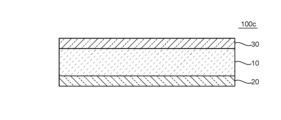
- the optical film 100c shown in FIG. 3 has a first transparent base material 20 on the first main surface side of the diffusion layer 10, and has a second transparent base material 30 on the second main surface side.
- the diffusion layer 10 and the first transparent base material 20 and/or the second transparent base material 30 may be laminated via an adhesive layer or a pressure-sensitive adhesive layer, or may be laminated directly without intervening therebetween. It's okay.
- the dispersed particles 14 include the liquid crystal compound 14a and the liquid crystal polymer 14b, but the dispersed particles 14 do not need to include the liquid crystal compound 14a. Furthermore, in the optical film according to the embodiment of the present invention, since the orientation of the liquid crystal compound in the dispersed particles can be controlled by the liquid crystal polymer, there is no need to control the orientation of the liquid crystal compound by applying a voltage. Therefore, the optical film according to the embodiment of the present invention does not need to have an electrode layer, regardless of whether the dispersed particles contain a liquid crystal compound.
- the orientation state of the liquid crystal polymer is not particularly limited as long as there are two or more orientation states.
- the orientation state of the liquid crystal polymer in a plurality of regions where the orientation state of the liquid crystal polymer is different is not limited, and can be independently determined as desired in each region.
- the orientation state may be as follows.
- the arrangement pattern of these regions is not limited and can be freely designed as a predetermined pattern. Therefore, the optical film can exhibit a desired haze in a desired pattern.
- the plurality of regions (A1, A2, B1, B2, C) in which the orientation states of the liquid crystal polymers in the dispersed particles are different each have a certain area, but each region has a predetermined area. It is not necessary to have an area larger than the value of .
- the orientation state of the liquid crystal polymer changes continuously in the in-plane direction, and a region in a particular orientation state cannot be identified as a region having a constant area in plan view.
- the diffusion layer is treated as having a plurality of regions in which the alignment states of the liquid crystal polymer are different.
- the orientation state of the liquid crystal polymer changes continuously in the in-plane direction. It can be seen as changing.
- the haze in the portions corresponding to the plurality of regions in which the orientation states of the liquid crystal polymers in the dispersed particles are different can be appropriately set depending on the use of the optical film.
- the difference between the maximum value and the minimum value of haze in the region corresponding to the plurality of regions is, for example, more than 0%, preferably 10% or more, more preferably 20% to 100%, and even more preferably can be between 30% and 100%.
- the maximum value of the haze may be, for example, 30% to 100%
- the minimum value of the haze may be, for example, 0% to 70%.
- the diffusion layer 10 includes a polymer matrix 12 and dispersed particles 14 that are dispersed in the polymer matrix 12 and include a liquid crystal polymer 14b that is a polymer of a polymerizable liquid crystal compound. It has a plurality of regions in which the orientation state of 14b is different.
- the dispersed particles 14 may further contain a liquid crystal compound 14a.
- the dispersed particles 14 include a liquid crystal compound 14a and a liquid crystal polymer 14b.
- the haze in each of the plurality of regions of the diffusion layer can be appropriately set depending on the use of the optical film, etc.
- the maximum value, the minimum value, and the difference between these haze values in the plurality of regions of the diffusion layer can be set so as to obtain the maximum value, the minimum value, and the difference between these values, which are desired for the optical film.
- the polymer matrix 12 may be composed of any suitable resin.
- the polymer matrix-forming resin can be appropriately selected depending on the light transmittance, the refractive index of the liquid crystal compound, the adhesive strength with the base material, and the like.
- water-soluble or water-dispersible resins such as urethane resins, polyvinyl alcohol resins, polyethylene resins, polypropylene resins, and acrylic resins can be preferably used.
- the polymer matrix-forming resins may be used alone or in combination.
- the content of the polymer matrix in the diffusion layer is, for example, 30% to 70% by weight, preferably 35% to 65% by weight, more preferably 40% to 60% by weight. If the content of the polymer matrix is within this range, effects such as good mechanical strength and prevention of liquid crystal leakage from the edges can be obtained.
- the liquid crystal polymer 14b is a polymer of polymerizable liquid crystal compounds and is non-liquid crystalline. That is, in a liquid crystal polymer, for example, transition to a liquid crystal phase, a glass phase, or a crystalline phase due to temperature change, which is characteristic of liquid crystal compounds, does not occur.
- the polymerizable liquid crystal compound constituting the liquid crystal polymer can be appropriately selected depending on light transmittance, compatibility with the non-polymerizable liquid crystal compound described below, and the like.
- the polymerizable liquid crystal compound may be a bifunctional or more crosslinked compound.
- Examples of polymerizable liquid crystal compounds include Japanese Patent Publication No. 2002-533742 (WO00/37585), EP358208 (US5211877), EP66137 (US4388453), WO93/22397, EP0261712, DE19504224, DE4408171, and G Polymerizable mesogenic compounds described in B2280445 etc. etc. can be used.
- a specific example of such a polymerizable mesogen compound is, for example, BASF's product name LC242.
- the polymerizable liquid crystal compound for example, a nematic liquid crystal monomer is preferable.
- any suitable non-polymerizable liquid crystal compound may be used as the liquid crystal compound 14a.
- the diffusion layer can be formed by performing a polymerization reaction while controlling the orientation of a polymerizable liquid crystal compound, but at that time, a non-polymerizable liquid crystal compound is combined with a polymerizable liquid crystal compound.
- the temperature range of the liquid crystal phase for example, nematic phase
- the alignment can be controlled more suitably.
- a non-polymerizable liquid crystal compound having a birefringence ⁇ n of 0.10 to 0.45 is used.
- the dielectric anisotropy of the non-polymerizable liquid crystal compound may be positive or negative.
- the non-polymerizable liquid crystal compound may be, for example, a nematic type, smectic type, or cholesteric type liquid crystal compound. It is preferable to use a nematic liquid crystal compound because it can achieve excellent transparency in a transparent state.
- Nematic liquid crystal compounds include biphenyl compounds, phenylbenzoate compounds, cyclohexylbenzene compounds, azoxybenzene compounds, azobenzene compounds, azomethine compounds, terphenyl compounds, biphenylbenzoate compounds, cyclohexylbiphenyl compounds, Examples include phenylpyridine compounds, cyclohexylpyrimidine compounds, cholesterol compounds, and fluorine compounds. These low molecular weight liquid crystal compounds may be used alone or in combination.
- the total content of the liquid crystal polymer and the liquid crystal compound if present in the diffusion layer is, for example, 30% to 70% by weight, preferably 35% to 65% by weight. , more preferably 40% to 60% by weight.
- the content ratio of the liquid crystal polymer to the total content of the liquid crystal polymer and the liquid crystal compound in the diffusion layer is, for example, 5% by weight or more, preferably 7% by weight or more, and more preferably 10% by weight. % or more, and for example, 100% by weight or less, preferably 80% by weight or less, more preferably 50% by weight or less.
- the total content of the polymer matrix, liquid crystal polymer, and liquid crystal compound when present in the diffusion layer may be, for example, 90% to 99.9% by weight, preferably 95% to 99.9% by weight. .
- the diffusion layer is a PDLC layer containing liquid crystal droplets containing a polymerizable liquid crystal compound and a non-polymerizable liquid crystal compound as an optional component. It can be formed by polymerizing the polymerizable liquid crystal compound while applying a voltage from the second principal surface side so that regions with different electric field strengths are generated. Therefore, the diffusion layer (more specifically, the dispersed particles) may further contain a polymerization initiator. The content ratio of the polymerization initiator is as described in Section B. Furthermore, unreacted polymerizable liquid crystal compounds may remain in the dispersed particles. The content of the unreacted polymerizable liquid crystal compound in the diffusion layer (more specifically, the dispersed particles) is, for example, 3% by weight or less, preferably 1% by weight or less.
- the average particle diameter of the dispersed particles may be, for example, 0.3 ⁇ m to 9 ⁇ m, preferably 0.4 ⁇ m to 8 ⁇ m. If the average particle diameter of the dispersed particles is too small, the dispersed particle size is smaller than the wavelength of light, so light passes through the dispersed particles without being scattered, resulting in the problem of not being able to obtain sufficient haze. may occur. Moreover, if the average particle diameter is too large, the dispersed particle size is too large than the wavelength of light, which may cause a problem that sufficient haze cannot be obtained. Note that the average particle diameter of the dispersed particles in the diffusion layer is the volume average particle diameter of the dispersed particles when viewed from a direction perpendicular to the main surface of the optical film.
- the thickness of the diffusion layer is typically 2 ⁇ m to 40 ⁇ m, preferably 3 ⁇ m to 35 ⁇ m, and more preferably 4 ⁇ m to 30 ⁇ m.
- the first transparent substrate 20 includes a first transparent film.
- the first transparent base material may have a hard coat layer on one side or both sides of the first transparent film, if necessary.
- the haze of the first transparent substrate is preferably 20% or less, more preferably 10% or less, and even more preferably 0.1% to 10%.
- the total light transmittance of the first transparent base material is preferably 30% or more, more preferably 60% or more, and still more preferably 80% or more. Total light transmittance can be measured according to JIS K 7361.
- the first transparent film may be formed using any suitable material. Specific examples include glass films and polymer films. Polymer films are preferred because they have excellent smoothness and can greatly improve productivity through continuous production using rolls.
- the polymer film is typically a polymer film whose main component is a thermoplastic resin.
- the thermoplastic resin include polyester resins; cycloolefin resins such as polynorbornene; acrylic resins; polycarbonate resins; cellulose resins, and the like. Among these, polyester resins, cycloolefin resins, and acrylic resins are preferred. These resins have excellent transparency, mechanical strength, thermal stability, moisture shielding properties, and the like.
- the above thermoplastic resins may be used alone or in combination of two or more.
- optical films such as those used in polarizing plates, such as low retardation base materials, high retardation base materials, retardation plates, absorption type polarizing films, polarized light selective reflection films, etc., as the first transparent base material. It is.
- the total light transmittance of the first transparent film is preferably 30% or more, more preferably 60% or more, and still more preferably 80% or more.
- the thickness of the first transparent film is preferably 200 ⁇ m or less, more preferably 3 ⁇ m to 150 ⁇ m, and even more preferably 5 ⁇ m to 100 ⁇ m.
- the second transparent base 30 includes a second transparent film.
- the second transparent base material may have a hard coat layer on one or both sides of the second transparent film, if necessary.
- the haze of the second transparent base material is preferably 20% or less, more preferably 10% or less, and even more preferably 0.1% to 10%.
- the total light transmittance of the second transparent base material is preferably 30% or more, more preferably 60% or more, and still more preferably 80% or more.
- the second transparent base material may have the same configuration as the first transparent base material, or may have a different configuration.
- the invention comprises a polymer matrix and dispersed particles that are dispersed in the polymer matrix and include a liquid crystal polymer that is a polymer of a polymerizable liquid crystal compound.
- a polymer film is provided that has a diffusion layer, and the diffusion layer has a plurality of regions having different content ratios of the liquid crystal polymer.
- the diffusion layer has a region containing dispersed particles containing a liquid crystal polymer and a region containing dispersed particles containing a polymerizable liquid crystal compound.
- the content ratio of the liquid crystal polymer in the region containing the dispersed particles containing the polymerizable liquid crystal compound is smaller than the content ratio of the liquid crystal polymer in the region containing the dispersed particles containing the liquid crystal polymer.
- the difference in the content ratio of the liquid crystal polymer is not limited as long as the effects of the present invention can be obtained.
- a region containing dispersed particles containing a polymerizable liquid crystal compound may be substantially free of liquid crystal polymer. In such a configuration, when the liquid crystal polymer and the polymerizable liquid crystal compound have different alignment states, these regions can exhibit different hazes.
- the haze in the portions corresponding to the plurality of regions having different content ratios of the liquid crystal polymer can be appropriately set depending on the use of the optical film, etc.
- the difference between the maximum value and the minimum value of haze in the region corresponding to the plurality of regions is, for example, more than 0%, preferably 10% or more, more preferably 20% to 100%, and even more preferably can be between 30% and 100%.
- the maximum value of the haze may be, for example, 30% to 100%
- the minimum value of the haze may be, for example, 0% to 70%.
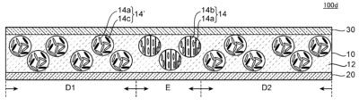
- FIG. 4 is a schematic cross-sectional view of an example of an optical film according to the second embodiment of the present invention.
- the optical film 100d includes a diffusion layer 10, a first transparent base material 20 disposed on the first main surface side of the diffusion layer 10, and a second transparent base material 30 disposed on the second main surface side.
- the diffusion layer 10 includes a region E including a polymer matrix 12 and first dispersed particles 14 that are dispersed in the polymer matrix 12 and include a non-polymerizable liquid crystal compound 14a and a liquid crystal polymer 14b; and regions D1 and D2 including second dispersed particles 14' which are dispersed in the polymer matrix 12 and include a non-polymerizable liquid crystal compound 14a and a polymerizable liquid crystal compound 14c.
- the second dispersed particles 14' may be droplets of liquid crystal compound.
- the non-polymerizable liquid crystal compound 14a and the liquid crystal polymer 14b are oriented substantially perpendicularly to the main surface.
- regions D1 and D2 the non-polymerizable liquid crystal compound 14a and the polymerizable liquid crystal compound 14c are in a non-aligned state. Therefore, regions D1 and D2 can exhibit higher haze than region E in plan view.
- the same explanation as in Section A-2 can be applied to the region containing the first dispersed particles 14.
- the region containing the second dispersed particles 14' the same explanation as in Section A-2 can be applied, except that the region contains the polymerizable liquid crystal compound 14c instead of the liquid crystal polymer 14b.
- the dispersed particles 14' may not contain the non-polymerizable liquid crystal compound 14a depending on the purpose.
- Sections A-3 and A-4 can be applied to the first transparent substrate 20 and the second transparent substrate 30, respectively. Depending on the purpose, either or both of the first transparent base material 20 and the second transparent base material 30 may be omitted.
- optical films according to embodiments of the present invention can exhibit a desired haze in a desired pattern. Therefore, specific examples of uses of optical films include diffusion films, decorative films, and the like.
- a preferred example of the diffusion film is a diffusion film for an image display device, more specifically, a diffusion film for an image display device equipped with a direct type backlight.
- a direct backlight with multiple LED light sources arranged at predetermined intervals, the haze in the area directly above the LED light source is high, and as the distance from the LED light source increases,
- an optical film patterned to reduce haze the in-plane luminance distribution can be suitably made uniform.
- a preferable example of the design film is a shielding film that shields wiring, etc. provided at the periphery of an image display area in an image display device such as a liquid crystal display device or an organic EL display device.
- wiring and the like are shielded by providing a frame-shaped printed layer on a front plate such as a cover glass or a cover film directly or via a base film.
- the interlayer adhesive cannot fully absorb the difference in thickness between the part where the printed layer is provided and the other parts, and air bubbles may be generated.
- the optical film according to the above since there is no difference in level between the shielding area (high haze area) and the display area (low haze area) and the area is smooth, the problem of bubbles can be solved.
- the method for manufacturing an optical film according to the first embodiment of the present invention includes: (Step A) Applying a coating liquid containing a polymer matrix-forming resin, a polymerizable liquid crystal compound, and a solvent to the first base material to obtain a coating layer; (Step B) Drying the coating layer to obtain a PDLC layer containing a polymer matrix and droplets containing the polymerizable liquid crystal compound dispersed in the polymer matrix, and (Step C) drying the coating layer. Polymerizing the polymerizable liquid crystal compound while applying a voltage so that regions with different electric field strengths are generated from the first main surface side and the second main surface side of the PDLC layer; including.
- the side of the PDLC layer or the diffusion layer is opposite to the side on which the first base material is provided. It may further include arranging a second substrate on the side (step D).
- the polymerizable liquid crystal compound polymerizes in different orientation states depending on the electric field strength in each region where the electric field strength is different, so that the orientation state of the liquid crystal polymer in the dispersed particles changes.
- a diffusion layer having different regions can be formed. Therefore, according to the method for manufacturing an optical film according to the first embodiment, the optical film described in Section A (specifically, the optical film of the first embodiment) can be suitably obtained.
- step A a coating liquid containing a polymer matrix-forming resin, a polymerizable liquid crystal compound, and a solvent is applied to the first base material to obtain a coating layer.
- the coating liquid may further contain a non-polymerizable liquid crystal compound.
- the above coating liquid is preferably an emulsion (hereinafter sometimes referred to as "emulsion coating liquid") containing liquid crystal particles containing a polymerizable liquid crystal compound and optionally a non-polymerizable liquid crystal compound as a dispersoid.
- the coating liquid is an emulsion coating liquid in which polymer matrix-forming resin particles, a polymerizable liquid crystal compound, and, optionally, liquid crystal particles containing a non-polymerizable liquid crystal compound are dispersed in a solvent.
- the emulsion coating liquid preferably further contains a polymerization initiator in the liquid crystal particles, and may further contain any suitable additive depending on the purpose.
- water or a mixed solvent of water and a water-miscible organic solvent can be preferably used.
- water-miscible organic solvents include C1-3 alcohol, acetone, DMSO, and the like.
- the polymerizable liquid crystal compound, non-polymerizable liquid crystal compound, and polymer matrix-forming resin are as described in Section A-2.
- Optional additives include dispersants, leveling agents, crosslinking agents, and the like.
- the content ratio of the liquid crystal compound in the solid content of the coating liquid is, for example, 30% to 70% by weight, preferably 35% by weight to It may be 65% by weight, more preferably 40% to 60% by weight.
- the weight ratio of the polymerizable liquid crystal compound to the non-polymerizable liquid crystal compound (polymerizable liquid crystal compound: non-polymerizable liquid crystal compound) in the coating liquid is, for example, 5:95 to 100:0, preferably 7:93 to 80: 20, more preferably 10:90 to 50:50.
- the content of the polymer matrix-forming resin in the solid content of the coating liquid may be, for example, 30% to 70% by weight, preferably 35% to 65% by weight, more preferably 40% to 60% by weight. .
- the matrix-forming resin may have a ratio of, for example, 30:70 to 70:30, preferably 35:65 to 65:35, more preferably 40:60 to 60:40.
- the total content of the polymer matrix-forming resin, the polymerizable liquid crystal compound, and the non-polymerizable liquid crystal compound when present in the solid content of the coating liquid is, for example, 90% to 99.9% by weight, preferably It can be from 95% to 99.9% by weight.
- the average particle diameter of the liquid crystal particles is preferably 0.3 ⁇ m or more, more preferably 0.4 ⁇ m or more. Further, the average particle diameter of the liquid crystal particles is preferably 9 ⁇ m or less, more preferably 8 ⁇ m or less. As long as the average particle diameter of the liquid crystal particles is within this range, the average particle diameter of the dispersed particles in the diffusion layer can be set within a desired range. Note that the average particle diameter of the liquid crystal particles is a volume average particle diameter.
- the average particle diameter of the liquid crystal particles preferably has a relatively narrow particle size distribution.
- the coefficient of variation (CV value) of the average particle diameter of the liquid crystal particles may be, for example, less than 0.40, preferably 0.35 or less, and more preferably 0.30 or less.
- the emulsion coating liquid is substantially free of liquid crystal particles having a particle size of less than 0.3 ⁇ m or more than 9 ⁇ m (e.g., the liquid crystal particles have a particle size of less than 0.3 ⁇ m or more than 9 ⁇ m based on the total volume of liquid crystal particles).
- An emulsion coating liquid in which the volume ratio of certain liquid crystal particles is 10% or less may be used.
- the average particle diameter of the resin particles for forming a polymer matrix is preferably 10 nm to 500 nm, more preferably 30 nm to 300 nm, and even more preferably 50 nm to 200 nm. Two or more types of resin particles having different resin types and/or different average particle sizes may be used.
- the average particle diameter of the resin particles for forming a polymer matrix means the volume average median diameter, and can be measured using a dynamic light scattering particle size distribution analyzer.
- any appropriate photopolymerization initiator or thermal polymerization initiator may be used depending on the purpose and desired properties, and a photopolymerization initiator is preferably used.
- Specific examples of photopolymerization initiators include 2,2-dimethoxy-2-phenylacetophenone, acetophenone, benzophenone, xanthone, 3-methylacetophenone, 4-chlorobenzophenone, 4,4'-dimethoxybenzophenone, benzoinpropyl ether, and benzyl.
- the polymerization initiators may be used alone or in combination of two or more.
- the content of the polymerization initiator is preferably 0.1 parts by weight to 10 parts by weight, more preferably 0.5 parts by weight to 5 parts by weight, based on 100 parts by weight of the polymerizable liquid crystal compound.
- dispersant examples include anionic surfactants, cationic surfactants, amphoteric surfactants, and nonionic surfactants.
- the content of the dispersant is preferably 0.05 parts by weight to 10 parts by weight, more preferably 0.1 parts by weight to 1 part by weight, based on 100 parts by weight of the emulsion coating liquid.
- leveling agent examples include acrylic leveling agents, fluorine leveling agents, silicone leveling agents, and the like.
- the content of the leveling agent is preferably 0.05 parts by weight to 10 parts by weight, more preferably 0.1 parts by weight to 1 part by weight, based on 100 parts by weight of the emulsion coating liquid.
- crosslinking agent examples include aziridine crosslinking agents, isocyanate crosslinking agents, and the like.
- the content of the crosslinking agent is preferably 0.5 parts by weight to 10 parts by weight, more preferably 0.8 parts by weight to 5 parts by weight, based on 100 parts by weight of the emulsion coating solution.
- the emulsion coating liquid includes, for example, a resin emulsion or resin particle dispersion containing resin particles for forming a polymer matrix, and a liquid crystal containing liquid crystal particles containing a polymerizable liquid crystal compound, a polymerization initiator, and optionally a non-polymerizable liquid crystal compound. It can be prepared by mixing the emulsion and any additives (eg, dispersant, leveling agent, crosslinking agent). If necessary, a solvent may be further added during mixing.
- additives eg, dispersant, leveling agent, crosslinking agent
- the emulsion coating solution can be prepared by adding a polymerizable liquid crystal compound, a polymer matrix-forming resin, a polymerization initiator, and optionally a non-polymerizable liquid crystal compound and additives to a solvent and mechanically dispersing the mixture. may also be prepared.
- the above resin emulsion and liquid crystal emulsion can be prepared by, for example, a mechanical emulsification method, a microchannel method, a membrane emulsification method, or the like.
- the liquid crystal emulsion is preferably prepared by a membrane emulsification method.
- the membrane emulsification method an emulsion with a uniform particle size distribution can be suitably obtained.
- the disclosures such as JP-A-4-355719 and JP-A-2015-40994 (these are incorporated herein by reference) can be referred to.
- the solid content concentration of the emulsion coating liquid may be, for example, 20% to 60% by weight, preferably 30% to 50% by weight.
- the viscosity of the emulsion coating liquid can be appropriately adjusted so that the coating on the first base material is suitably performed.
- the viscosity of the emulsion coating liquid during application is preferably 20 mPas to 400 mPas, more preferably 30 mPas to 300 mPas, even more preferably 40 mPas to 200 mPas.
- the viscosity is less than 20 mPas, convection of the solvent becomes significant when drying the solvent, and the thickness of the PDLC layer (as a result, the diffusion layer) may become unstable.
- the viscosity exceeds 400 mPas, there is a possibility that the beads of the emulsion coating liquid will not be stable.
- the viscosity of the emulsion coating liquid can be measured, for example, using a rheometer MCR302 manufactured by Anton Paar.
- the viscosity here uses the value of shear viscosity under the conditions of 20° C. and a shear rate of 1000 (1/s).
- any suitable base material may be used as the first base material.
- the first transparent base material described in Section A-3 as the first base material, an optical film having the first transparent base material and a diffusion layer can be suitably obtained.
- the first base material may be peeled off and removed from the diffusion layer after step C is completed.
- any suitable method can be adopted as the coating method. Examples include roll coating, spin coating, wire bar coating, dip coating, die coating, curtain coating, spray coating, knife coating (comma coating, etc.). Among these, the roll coating method is preferred. For example, regarding coating by a roll coating method using a slot die, reference can be made to the description in JP-A-2019-5698.
- the thickness of the coating layer is preferably 3 ⁇ m to 40 ⁇ m, more preferably 4 ⁇ m to 30 ⁇ m, and even more preferably 5 ⁇ m to 20 ⁇ m. Within this range, a PDLC layer (as a result, a diffusion layer) with excellent thickness uniformity can be obtained.
- step B the coating layer is dried to obtain a PDLC layer containing a polymer matrix and droplets containing a polymerizable liquid crystal compound and optionally a non-polymerizable liquid crystal compound dispersed in the polymer matrix.
- the solvent is removed from the coating layer by drying, and the polymer matrix-forming resin particles are fused to each other, thereby forming a PDLC layer having a structure in which liquid crystal droplets are dispersed in the polymer matrix.
- Drying of the coating layer may be performed by any suitable method. Specific examples of the drying method include natural drying, heat drying, hot air drying, and the like.
- the emulsion coating liquid contains a crosslinking agent, a crosslinked structure of the polymer matrix may be formed during drying.
- the drying temperature is preferably 20°C to 150°C, more preferably 25°C to 80°C.
- the drying time is preferably 1 minute to 100 minutes, more preferably 2 minutes to 10 minutes.
- step C the polymerizable liquid crystal compound is polymerized while applying voltage from the first main surface side and the second main surface side of the PDLC layer so that regions with different electric field strengths are generated.
- a diffusion layer is formed that includes a polymer matrix and dispersed particles that are dispersed in the polymer matrix and include a liquid crystal polymer that is a polymer of a polymerizable liquid crystal compound.
- the polymerization of the polymerizable liquid crystal compound is performed by active energy ray irradiation, heating, or a combination thereof, and preferably by active energy ray irradiation.
- active energy rays ultraviolet rays, infrared rays, X-rays, ⁇ -rays, ⁇ -rays, ⁇ -rays, electron beams, etc. are used. Among these, ultraviolet light is preferred. Moreover, it is preferable that the active energy ray is collimated light that travels straight from the irradiation source.
- the ultraviolet irradiation conditions can be appropriately set depending on the type of polymerizable liquid crystal compound, the transmittance of the base material, the absorption wavelength of the photopolymerization initiator, and the like.
- the irradiation intensity can be, for example, from 0.1 mW/cm 2 to 1000 mW/cm 2 , preferably from 1 mW/cm 2 to 100 mW/cm 2 .
- the irradiation amount may be, for example, 10 mJ/cm 2 to 10000 mJ/cm 2 , preferably 100 mJ/cm 2 to 5000 mJ/cm 2 .
- the irradiation temperature can be, for example, -20°C to 80°C, preferably -20°C to 60°C.
- the voltage is applied using a first electrode placed on the first main surface side of the PDLC layer and a second electrode placed on the second main surface side, and the first electrode and the second electrode are placed on the second main surface side.
- the distance from the second electrode regions with different electric field strengths are formed.
- process C will be explained with reference to FIG.
- Step D is performed before Step C, and the first transparent base material 20 as the first base material is arranged on the first main surface side of the PDLC layer 10a.
- a second transparent base material 30 serving as a second base material is disposed on the second main surface side.
- the first main surface and/or the second main surface of the PDLC layer may be exposed.
- FIG. 5(a) is a schematic cross-sectional view showing the PDLC layer obtained in step B in a state where no voltage is applied.
- the PDLC layer 10a includes a polymer matrix 12 and liquid crystal droplets 14' dispersed in the polymer matrix 12, and the liquid crystal droplets 14' include a non-polymerizable liquid crystal compound 14a and a polymerizable liquid crystal compound 14c.
- the first electrode 40 is arranged on the outside of the first transparent base material 20 (the side opposite to the side where the PDLC layer is arranged), and the first electrode 40 is arranged on the outside of the second transparent base material 30 (the side opposite to the side where the PDLC layer is arranged).
- a second electrode 50 that can transmit active energy rays is arranged on the side).
- the non-polymerizable liquid crystal compound 14a and the polymerizable liquid crystal compound 14c in the liquid crystal droplet 14' are non-polymerizable. Exists in an oriented state. Further, the first electrode 40 is formed so that the surface height on the PDLC layer 10a side differs depending on the region, thereby forming regions with different inter-electrode distances.
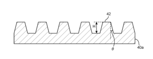
- the region where the distance between the electrodes is different can be freely designed by, for example, changing the surface shape of the first electrode and/or the second electrode on the PDLC layer side. Specifically, by providing unevenness, steps, slopes, etc. in any pattern on the surfaces of the first electrode and/or the second electrode, a desired distance between the electrodes can be achieved in a desired pattern. For example, as shown in FIG. 6, by providing a tapered convex portion 42 on the surface of the electrode 40a, the distance between the electrodes can be changed continuously, and as a result, the polymerizable liquid crystal compound in the liquid crystal droplet And the orientation state of the non-polymerizable liquid crystal compound can be changed continuously within the plane.
- the resulting optical film has a haze with an arbitrary slope.
- the height H and the inclination angle ⁇ can each be set to any appropriate value depending on the haze pattern desired for the optical film.
- FIG. 5(b) is a schematic diagram showing an embodiment in which the polymerizable liquid crystal compound 14c is polymerized by UV irradiation.
- UV irradiation is performed while a voltage is applied between the first electrode 40 and the second electrode 50 from the power source 60.
- a voltage is applied between the first electrode 40 and the second electrode 50 from the power source 60.
- an electric field with an intensity corresponding to the separation distance between the first electrode 40 and the second electrode 50 is generated, resulting in a plurality of regions having different electric field intensities.
- the non-polymerizable liquid crystal compound 14a and the polymerizable liquid crystal compound 14c in the liquid crystal droplet 14' are oriented according to the electric field strength.
- the non-polymerizable liquid crystal compound 14a and the polymerizable liquid crystal compound 14c are aligned approximately perpendicularly to the main surface of the PDLC layer 10a. , the degree of orientation becomes weaker as the separation distance increases.
- a diffusion layer 10 having a plurality of regions in which the orientation states of the liquid crystal polymer 14b in the dispersed particles 14 are different is formed. Ru.
- the voltage applied during polymerization is not limited as long as the polymerizable liquid crystal compound shows the desired orientation, and can be appropriately set depending on the desired haze of the optical film, the separation distance between the electrodes, etc.
- the voltage may be, for example, between 10V and 100kV, preferably between 100V and 10kV.
- step D a second base material is arranged on the side (first main surface side) of the PDLC layer or diffusion layer opposite to the side on which the first base material is provided (first main surface side).
- Any suitable base material can be used as the first base material, and the second transparent base material described in Section A-4 can be preferably used.
- the timing to perform step D may be before step C, that is, before polymerizing the polymerizable liquid crystal compound, or after step C, that is, after polymerizing the polymerizable liquid crystal compound. .
- the first transparent substrate described in section A-3 and the transparent substrate described in section A-4 are used as the first base material and the second base material, respectively.
- the second transparent base material By using the second transparent base material, an optical film having the first transparent base material, the second transparent base material, and a diffusion layer directly sandwiched between them can be obtained.
- the second base material is preferably laminated using a laminator at a lamination pressure of 0.006 MPa/m to 7 MPa/m, more preferably 0.06 MPa/m to 0.7 MPa/m. It is laminated on the second main surface side of the PDLC layer or diffusion layer while applying a laminating pressure of .
- the method for manufacturing an optical film according to the second embodiment of the present invention includes: (Step I) Applying a coating liquid containing a polymer matrix-forming resin, a polymerizable liquid crystal compound, and a solvent to the first base material to obtain a coating layer; (Step II) Drying the coating layer to obtain a polymer-dispersed liquid crystal layer containing a polymer matrix and droplets containing the polymerizable liquid crystal compound dispersed in the polymer matrix, and ( Step III) irradiating a predetermined region with active energy rays while applying a voltage to the polymer dispersed liquid crystal layer to polymerize the polymerizable liquid crystal compound; including.
- the side of the PDLC layer or the diffusion layer opposite to the first base material is provided. It may further include placing a second substrate on the side (step IV).
- a liquid crystal polymer with a fixed oriented state is produced.
- the polymerizable liquid crystal compound does not polymerize and becomes a non-aligned state when no voltage is applied.
- a diffusion layer is formed that has multiple regions with different proportions of liquid crystal polymer, and the haze of the area with a high content of liquid crystal polymer (irradiated area) is higher than the haze of the area with a small content of liquid crystal polymer (non-irradiated area). It gets lower.
- the optical film described in Section A (for example, the optical film of the second embodiment) can be suitably obtained.
- an optical film in which the boundary between the irradiated area and the non-irradiated area is clear and the haze contrast between these areas is high can be obtained.
- Step A, Step B, and Step D of the method for manufacturing an optical film according to the first embodiment can be applied to Step I, Step II, and Step IV, respectively.
- a photopolymerization initiator is used as the polymerization initiator.
- step III with a voltage applied to the PDLC layer, a predetermined region is irradiated with active energy rays to polymerize the polymerizable liquid crystal compound.
- active energy ray irradiation is performed through a photomask having openings in a predetermined pattern.
- active energy rays ultraviolet rays, infrared rays, X-rays, ⁇ -rays, ⁇ -rays, ⁇ -rays, electron beams, etc. are used. Among these, ultraviolet light is preferred. Moreover, it is preferable that the active energy ray is collimated light that travels straight from the irradiation source.
- the ultraviolet irradiation conditions may be the same as those described in the method for manufacturing an optical film according to the first embodiment.
- FIG. 7 is a schematic diagram illustrating one embodiment of step III.
- Step IV is performed before Step III, and the first transparent base material 20 as the first base material is arranged on the first main surface side of the PDLC layer 10a.
- a second transparent base material 30 serving as a second base material is disposed on the second main surface side.
- the first main surface and/or the second main surface of the PDLC layer may be exposed.
- the PDLC layer 10a includes a polymer matrix 12 and liquid crystal droplets 14' dispersed in the polymer matrix 12, and the liquid crystal droplets 14' include a non-polymerizable liquid crystal compound 14a and a polymerizable liquid crystal compound 14c.
- the first electrode 40 is arranged on the outside of the first transparent base material 20 (the side opposite to the side where the PDLC layer is arranged), and the first electrode 40 is arranged on the outside of the second transparent base material 30 (the side opposite to the side where the PDLC layer is arranged).
- a second electrode 50 that can transmit active energy rays is arranged on the side).
- a voltage is applied to the electrodes 40 and 50 from the power source 60, and an electric field is generated between them, so that the non-polymerizable liquid crystal compound 14a in the liquid crystal droplet 14'
- the liquid crystal compound 14c is oriented in a substantially vertical direction.
- the orientation state of the non-polymerizable liquid crystal compound 14a and the polymerizable liquid crystal compound 14c is uniform throughout the PDLC layer.
- active energy rays (ultraviolet rays in the illustrated example) are irradiated through a photomask 70 having openings in a predetermined pattern.
- the polymerizable liquid crystal compound 14c in the irradiated area is polymerized to produce a liquid crystal polymer 14b.
- the irradiated area of the diffusion layer 10 includes the first dispersed particles 14 containing the non-polymerizable liquid crystal compound 14a and the liquid crystal polymer 14b, and the non-irradiated area includes second dispersed particles (liquid crystal droplets) 14' containing a non-polymerizable liquid crystal compound 14a and a polymerizable liquid crystal compound 14c.
- the alignment state of the liquid crystal polymer 14b is fixed, and the non-polymerizable liquid crystal compound 14a is aligned along the liquid crystal polymer 14b.
- the illuminated area may exhibit a lower haze than the non-illuminated area.
- the voltage applied during polymerization is not limited as long as the polymerizable liquid crystal compound shows the desired orientation, and can be appropriately set depending on the desired haze of the optical film, the separation distance between the electrodes, etc.
- the voltage may be, for example, between 10V and 100kV, preferably between 100V and 10kV.
- the non-irradiated area may be irradiated with active energy rays in a state where no voltage is applied.
- the polymerizable liquid crystal compound contained in the non-irradiated area can be polymerized in a non-oriented state to produce a liquid crystal polymer.
- the polymerizable liquid crystal compound may be polymerized through a photomask with no voltage applied, and then the non-irradiated area may be irradiated with active energy rays with no voltage applied.
- the method for manufacturing an optical film according to the third embodiment of the present invention is as follows: (Step I) Applying a coating liquid containing a polymer matrix-forming resin, a polymerizable liquid crystal compound, and a solvent to the first base material to obtain a coating layer; (Step II) drying the coating layer to obtain a polymer-dispersed liquid crystal layer containing a polymer matrix and droplets containing the polymerizable liquid crystal compound dispersed in the polymer matrix; (Step III ⁇ ) irradiating a predetermined region with active energy rays to polymerize the polymerizable liquid crystal compound without applying a voltage to the polymer dispersed liquid crystal layer; (Step III ⁇ ) irradiating the remaining region with active energy rays while applying a voltage to the polymer dispersed liquid crystal layer to polymerize the polymerizable liquid crystal compound; including.
- the PDLC layer or the diffusion layer is placed on the opposite side of the first base material. It may further include placing a second substrate on the side (step IV). According to these methods, the optical film described in Section A (specifically, the optical film of the first embodiment) can be suitably obtained.
- Thickness Measured using a digital micrometer (manufactured by Anritsu Corporation, product name "KC-351C”).
- Volume average particle diameter of liquid crystal particles in liquid crystal emulsion 0.1% by weight of liquid crystal emulsion was added to 200 ml of an electrolyte aqueous solution (manufactured by Coulter, "Isoton II"), and the resulting mixed solution was used as a measurement sample using a multisizer.
- Example 1 (Preparation of emulsion coating liquid)
- a dispersant Noogen ET159, manufactured by Dai-ichi Kogyo Seiyaku Co., Ltd.
- leveling agent manufactured by DIC, product name "F-444
- emulsion coating liquid (Application and drying of emulsion coating liquid) The above emulsion coating liquid was applied to one side of a PET film (thickness: 125 ⁇ m) as a first transparent substrate to form a coating layer with a thickness of 20 ⁇ m. Coating was performed using a slot die, and the line speed was 6 m/min. Next, the coating layer was dried at 25° C. for 8 minutes to form a PDLC layer with a thickness of 8 ⁇ m.
- a PET film (thickness: 125 ⁇ m) as a second transparent base material was laminated on the PDLC layer while applying a lamination pressure of 0.4 MPa/m using a laminator. Thereby, a laminate having the configuration of [first transparent base material/PDLC layer/second transparent base material] was obtained. The obtained laminate exhibited uniform haze (haze: 90%) over the entire main surface.
- the first electrode As the first electrode, a flat metal electrode having a recess with a depth of 2 mm on the upper surface was used. The above laminate was placed so that the first transparent base material was in contact with the upper surface of the first electrode, and a glass substrate with ITO was placed thereon as a second electrode so that the ITO surface was in contact with the second transparent base material. . Next, while applying a voltage of 2 kV to these electrodes using a high-voltage power supply, a voltage of 10 mW/cm 2 was applied under a UV-LED lamp (manufactured by Hamamatsu Photonics, product name "C11924-101", peak wavelength 365 nm). The film was exposed to light at 25° C. for 10 minutes.
- a UV-LED lamp manufactured by Hamamatsu Photonics, product name "C11924-101", peak wavelength 365 nm
- the polymerizable liquid crystal compound was polymerized to obtain an optical film having the configuration of [first transparent base material/diffusion layer/second transparent base material].
- the inter-electrode distance in the region (region I) corresponding to the recess of the first electrode was about 2250 ⁇ m, and the electric field strength was 0.89 V/ ⁇ m.
- the inter-electrode distance in the region (region II) corresponding to the region other than the recessed portion of the first electrode was about 250 ⁇ m, and the electric field strength was 7.8 V/ ⁇ m.
- the haze in region I was 90%, and the haze in region II was 8%. From this, it can be seen that the orientation state of the liquid crystal polymer and liquid crystal compound in the dispersed particles in region I of the diffusion layer is different from the orientation state of the liquid crystal polymer and liquid crystal compound in the dispersed particles in region II. It can be seen that the degree of orientation of the liquid crystal polymer and liquid crystal compound in the dispersed particles in region I is lower than that in region II.
- optical film of the present invention can be suitably used in various applications such as a diffusion film and a decorative film.
- Optical film 100 Optical film 10 Diffusion layer 12 Polymer matrix 14 Dispersed particles 14' Liquid crystal droplets 14a Liquid crystal compound (non-polymerizable liquid crystal compound) 14b Liquid crystal polymer 14c Polymerizable liquid crystal compound 20 First transparent base material 30 Second transparent base material 40 First electrode 50 Second electrode 60 Power supply
Landscapes
- Physics & Mathematics (AREA)
- Chemical & Material Sciences (AREA)
- Nonlinear Science (AREA)
- Crystallography & Structural Chemistry (AREA)
- General Physics & Mathematics (AREA)
- Optics & Photonics (AREA)
- Mathematical Physics (AREA)
- Engineering & Computer Science (AREA)
- Dispersion Chemistry (AREA)
- Organic Chemistry (AREA)
- Materials Engineering (AREA)
- Spectroscopy & Molecular Physics (AREA)
- Life Sciences & Earth Sciences (AREA)
- Wood Science & Technology (AREA)
- Optical Elements Other Than Lenses (AREA)
Abstract
Description
1つの実施形態において、上記複数の領域が、所定のパターンで配列している。
1つの実施形態において、平面視において、上記複数の領域に対応する部位のヘイズの差の最大値が、10%以上である。
1つの実施形態において、上記分散粒子が、液晶化合物をさらに含む。
1つの実施形態において、上記液晶ポリマーと上記液晶化合物との合計含有量に対する上記液晶ポリマーの含有割合が、5重量%以上である。
1つの実施形態において、上記拡散層における上記液晶ポリマーおよび存在する場合の上記液晶化合物の合計含有割合が、30重量%~70重量%である。
1つの実施形態において、上記拡散層の第1主面側に第1の透明基材が配置されている。
1つの実施形態において、上記拡散層の第2主面側に第2の透明基材が配置されている。
1つの実施形態において、上記光学フィルムは、電極層を有さない。
本発明の別の局面によれば、高分子マトリクスと、該高分子マトリクス中に分散し、重合性液晶化合物の重合体である液晶ポリマーを含む分散粒子と、を含む拡散層を有し、平面視において、該液晶ポリマーの配向状態に応じて異なるヘイズを示す複数の領域を有する、光学フィルムが提供される。
本発明の別の局面によれば、高分子マトリクスと、該高分子マトリクス中に分散している分散粒子と、を含む、拡散層を有し、該拡散層が、重合性液晶化合物を含む分散粒子を含む領域と、該重合性液晶化合物の重合体である液晶ポリマーを含む分散粒子を含む領域と、を有し、平面視において、これらの領域が互いに異なるヘイズを示す、光学フィルムが提供される。
本発明の別の局面によれば、第1の基材に、高分子マトリクス形成用樹脂と重合性液晶化合物と溶媒とを含む塗工液を塗工して、塗布層を得ること、該塗布層を乾燥させて、高分子マトリクスと、該高分子マトリクス中に分散した該重合性液晶化合物を含む液滴と、を含む高分子分散型液晶層を得ること、および、該高分子分散型液晶層の第1主面側および第2主面側から、電界強度が異なる領域が生じるように電圧を印加しながら、該重合性液晶化合物を重合させること、を含む、光学フィルムの製造方法が提供される。
1つの実施形態において、上記電圧の印加が、上記高分子分散型液晶層の第1主面側に配置された第1電極と第2主面側に配置された第2電極とを用いて行われ、電界強度が異なる領域が生じるように、該第1電極と第2電極との離間距離を制御する。
本発明の別の局面によれば、第1の基材に、高分子マトリクス形成用樹脂と重合性液晶化合物と溶媒とを含む塗工液を塗工して、塗布層を得ること、該塗布層を乾燥させて、高分子マトリクスと、該高分子マトリクス中に分散した該重合性液晶化合物を含む液滴と、を含む高分子分散型液晶層を得ること、および、該高分子分散型液晶層に電圧を印加した状態で、所定の領域に活性エネルギー線を照射して該重合性液晶化合物を重合させること、を含む、光学フィルムの製造方法が提供される。
1つの実施形態において、上記塗工液が、上記重合性液晶化合物を含む液晶粒子を分散質として含むエマルションである。
1つの実施形態において、上記塗工液が、非重合性液晶化合物をさらに含む。
本発明の第1の実施形態によれば、高分子マトリクスと、該高分子マトリクス中に分散し、重合性液晶化合物の重合体である液晶ポリマーを含む分散粒子と、を含む拡散層を有し、該拡散層が、該液晶ポリマーの配向状態が異なる複数の領域を有する、光学フィルムが提供される。分散粒子は、液晶化合物をさらに含むことができる。分散粒子内で液晶化合物は液晶ポリマーに沿って配向し得る。よって、分散粒子は、その中に含まれる液晶ポリマーの配向状態に応じて異なる散乱性を示すことができ、このような構成を有する光学フィルムは、該複数の領域において液晶ポリマーの配向状態に応じた散乱度合い(ヘイズ)を示すことができる。よって、第1の実施形態の光学フィルムにおいては、平面視において、光学フィルム(より具体的には、拡散層)に散乱度合い(ヘイズ)が異なる複数の領域が存在する場合、「拡散層が、液晶ポリマーの配向状態が異なる複数の領域を有する」ということができる。さらにまた、第1の実施形態の光学フィルムは、高分子マトリクスと、該高分子マトリクス中に分散し、重合性液晶化合物の重合体である液晶ポリマーを含む分散粒子と、を含む拡散層を有し、平面視において、該液晶ポリマーの配向状態に応じて異なるヘイズを示す複数の領域を有する、光学フィルムであり得る。
図1(a)は、第1の実施形態による光学フィルムの一例の概略平面図であり、(b)は、(a)で示す光学フィルムの概略断面図である。光学フィルム100aは、高分子マトリクス12と、高分子マトリクス12中に分散し、液晶化合物14aと液晶ポリマー14bとを含む分散粒子14と、を含む拡散層10から構成されている。拡散層10は、5つの領域(A1、A2、B1、B2、C)を有する。これらの領域中、領域A1およびA2における液晶ポリマー14bの配向状態は互いに同じであり、領域B1およびB2における液晶ポリマー14bの配向状態は互いに同じであり、領域A1およびA2と、領域B1およびB2と、領域Cとにおける液晶ポリマー14bの配向状態は互いに異なっている(各領域の配向状態の関係:A1=A2≠B1=B2≠C)。
拡散層10は、高分子マトリクス12と、高分子マトリクス12中に分散し、重合性液晶化合物の重合体である液晶ポリマー14bを含む分散粒子14とを含み、分散粒子14中の液晶ポリマー14bの配向状態が異なる複数の領域を有する。分散粒子14は、液晶化合物14aをさらに含んでいてもよい。例えば、図1に示す実施形態では、分散粒子14は、液晶化合物14aと液晶ポリマー14bとを含んでいる。また、拡散層10は、領域A1、A2、B1、B2、およびCを有し、各領域の分散粒子14中の液晶ポリマー14bの配向状態は「A1=A2≠B1=B2≠C」の関係にある。すなわち、領域A1およびA2と、領域B1およびB2と、領域Cとにおける液晶ポリマー14bの配向状態は互いに異なっている。また、分散粒子14中の液晶化合物14aは、液晶ポリマー14bに沿って配向している。このような構成によれば、分散粒子14中の液晶ポリマー14bの配向状態が異なる領域は互いに異なるヘイズを示し得る。よって、拡散層10の各領域のヘイズは「A1=A2≠B1=B2≠C」の関係を満たし得る。
第1の透明基材20は、第1の透明フィルムを含む。第1の透明基材は、必要に応じて、第1の透明フィルムの片側または両側にハードコート層を有していてもよい。
第2の透明基材30は、第2の透明フィルムを含む。第2の透明基材は、必要に応じて、第2の透明フィルムの片側または両側にハードコート層を有していてもよい。
本発明の第2の実施形態によれば、高分子マトリクスと、該高分子マトリクス中に分散し、重合性液晶化合物の重合体である液晶ポリマーを含む分散粒子と、を含む拡散層を有し、該拡散層が、該液晶ポリマーの含有割合が異なる複数の領域を有する、高分子フィルムが提供される。代表的には、拡散層は、液晶ポリマーを含む分散粒子を含む領域と、重合性液晶化合物を含む分散粒子を含む領域とを有する。上記重合性液晶化合物を含む分散粒子を含む領域における液晶ポリマーの含有割合は、上記液晶ポリマーを含む分散粒子を含む領域における液晶ポリマーの含有割合よりも小さい。液晶ポリマーの含有割合の差は、本発明の効果が得られる限りにおいて制限されない。例えば、重合性液晶化合物を含む分散粒子を含む領域は、液晶ポリマーを実質的に含まなくてもよい。このような構成において、液晶ポリマーと重合性液晶化合物とが異なる配向状態をとることにより、これらの領域は互いに異なるヘイズを示すことができる。
本発明の実施形態による光学フィルムは、所望のパターンで所望のヘイズを示し得る。よって、光学フィルムの用途の具体例としては、拡散フィルム、意匠性フィルム等が挙げられる。
本発明の第1の実施形態による光学フィルムの製造方法は、
(工程A)第1の基材に、高分子マトリクス形成用樹脂と重合性液晶化合物と溶媒とを含む塗工液を塗工して、塗布層を得ること、
(工程B)該塗布層を乾燥させて、高分子マトリクスと、該高分子マトリクス中に分散した該重合性液晶化合物を含む液滴と、を含むPDLC層を得ること、および
(工程C)該PDLC層の第1主面側および第2主面側から、電界強度が異なる領域が生じるように電圧を印加しながら、該重合性液晶化合物を重合させること、
を含む。
第1の実施形態による光学フィルムの製造方法は、必要に応じて、重合性液晶化合物を重合させる前または重合させた後に、PDLC層または拡散層の第1の基材が設けられた側と反対側に第2の基材を配置すること(工程D)をさらに含み得る。第1の実施形態による光学フィルムの製造方法によれば、電界強度が異なる各領域において重合性液晶化合物が電界強度に応じた異なる配向状態で重合する結果、分散粒子中の液晶ポリマーの配向状態が異なる複数の領域を有する拡散層が形成され得る。よって、第1の実施形態による光学フィルムの製造方法によれば、A項に記載の光学フィルム(具体的には、第1の実施形態の光学フィルム)が好適に得られ得る。
工程Aにおいては、第1の基材に、高分子マトリクス形成用樹脂と重合性液晶化合物と溶媒とを含む塗工液を塗工して、塗布層を得る。塗工液は非重合性液晶化合物をさらに含み得る。
工程Bにおいては、塗布層を乾燥させて、高分子マトリクスと、該高分子マトリクス中に分散した重合性液晶化合物および任意に非重合性液晶化合物を含む液滴と、を含むPDLC層を得る。乾燥により塗布層から溶媒が除去されて、高分子マトリクス形成用樹脂粒子が互いに融着し合うことにより、高分子マトリクス中に液晶液滴が分散した構造を有するPDLC層が形成される。
工程Cにおいては、PDLC層の第1主面側および第2主面側から、電界強度が異なる領域が生じるように電圧を印加しながら、重合性液晶化合物を重合させる。これにより、高分子マトリクスと、該高分子マトリクス中に分散し、重合性液晶化合物の重合体である液晶ポリマーを含む分散粒子と、を含む拡散層が形成される。
工程Dにおいては、PDLC層または拡散層の第1の基材が設けられた側(第1主面側)と反対側(第2主面側)に第2の基材を配置する。第1の基材としては、任意の適切な基材が用いられ得、A-4項に記載の第2の透明基材が好ましく用いられ得る。工程Dを実施するタイミングは、工程Cの前、すなわち、重合性液晶化合物を重合させる前であってもよく、工程Cの後、すなわち、重合性液晶化合物を重合させた後であってもよい。
(工程I)第1の基材に、高分子マトリクス形成用樹脂と重合性液晶化合物と溶媒とを含む塗工液を塗工して、塗布層を得ること、
(工程II)該塗布層を乾燥させて、高分子マトリクスと、該高分子マトリクス中に分散した該重合性液晶化合物を含む液滴と、を含む高分子分散型液晶層を得ること、および
(工程III)該高分子分散型液晶層に電圧を印加した状態で、所定の領域に活性エネルギー線を照射して該重合性液晶化合物を重合させること、
を含む。
第2の実施形態による光学フィルムの製造方法は、必要に応じて、重合性液晶化合物を重合させる前または重合させた後に、PDLC層または拡散層の第1の基材が設けられた側と反対側に第2の基材を配置すること(工程IV)をさらに含み得る。第2の実施形態による光学フィルムの製造方法によれば、活性エネルギー線が照射された領域において重合性液晶化合物が配向状態で重合することから、配向状態が固定された液晶ポリマーが生成する。一方、活性エネルギー線が照射されなかった領域においては、重合性液晶化合物は重合せず、電圧が印加されていない状態では非配向状態になる。結果として、液晶ポリマーの含有割合が異なる複数の領域を有する拡散層が形成され、液晶ポリマーの含有割合が大きい領域(照射領域)のヘイズは含有割合が小さい領域(非照射領域)のヘイズよりも低くなる。第2の実施形態による光学フィルムの製造方法によれば、A項に記載の光学フィルム(例えば、第2の実施形態の光学フィルム)が好適に得られ得る。また、第2の実施形態による光学フィルムの製造方法によれば、照射領域と非照射領域と境界が明瞭であり、これらの領域のヘイズのコントラストが高い光学フィルムが好適に得られ得る。
あるいは、工程IIIにおいて、電圧無印加状態でフォトマスクを介した重合性液晶化合物の重合を行い、その後、電圧印加状態で非照射領域に活性エネルギー線照射を行ってもよい。すなわち、本発明の第3の実施形態の光学フィルムの製造方法は、
(工程I)第1の基材に、高分子マトリクス形成用樹脂と重合性液晶化合物と溶媒とを含む塗工液を塗工して、塗布層を得ること、
(工程II)該塗布層を乾燥させて、高分子マトリクスと、該高分子マトリクス中に分散した該重合性液晶化合物を含む液滴と、を含む高分子分散型液晶層を得ること、
(工程IIIα)該高分子分散型液晶層に電圧を印加しない状態で、所定の領域に活性エネルギー線を照射して該重合性液晶化合物を重合させること、
(工程IIIβ)該高分子分散型液晶層に電圧を印加した状態で、残りの領域に活性エネルギー線を照射して該重合性液晶化合物を重合させること、
を含む。
第3の実施形態による光学フィルムの製造方法は、必要に応じて、重合性液晶化合物を重合させる前または重合させた後に、PDLC層または拡散層の第1の基材が設けられた側と反対側に第2の基材を配置すること(工程IV)をさらに含み得る。
これらの方法によれば、A項に記載の光学フィルム(具体的には、第1の実施形態の光学フィルム)が好適に得られ得る。
デジタルマイクロメーター(アンリツ社製、製品名「KC-351C」)を用いて測定した。
(2)液晶エマルション中の液晶粒子の体積平均粒子径
電解質水溶液(コールター社製、「アイソトンII」)200mlに液晶エマルションを0.1重量%添加し、得られた混合液を測定試料としてマルチサイザー3(コールター社製、アパーチャーサイズ=20μm)を用いて、0.4μmから12μmまで対数基準で等間隔に256分割し離散化した粒子径ごとの体積の統計を取り、体積平均粒子径を算出した。なお、12μm以上の粒子が存在している場合は、アパーチャーサイズを30μmとし、0.6μmから18μmまで対数基準で等間隔に256分割し離散化した粒子径ごとの体積の統計を取ることで、体積平均粒子径を算出した。
(3)樹脂粒子の平均粒子径
100mLの水に樹脂分散体を数滴加えて測定試料を調製した。動的光散乱式粒子径分布測定装置(Microtrac社製、装置名「Nanotrac150」)を用いて、装置の測定ホルダに測定試料をセットし、測定可能な濃度であることを装置のモニタにて確認後に測定を行った。
(4)ヘイズ
日本電色社製 製品名「NDH4000」を用い、JIS K 7136に基づいて測定した。
(エマルション塗工液の作製)
非重合性液晶化合物(JNC社製、製品名「LX-153XX」、複屈折Δn=0.149(ne=1.651,no=1.502)、粘度=48.5mPa・s)53.7部、重合性液晶化合物(BASF社製、製品名「PALIOCOLOR LC-242」)5.9部、光重合開始剤(IGM社製、製品名「OMNIRAD651」)0.1部、純水39.8部、および分散剤(第一工業製薬社製、「ノイゲンET159」)0.5部を混合し、ホモジナイザーにて100rpmで10分攪拌することにより液晶エマルションを調製した。得られた液晶エマルション中の液晶粒子の平均粒子径は、3.4μmであった。
上記液晶エマルション38.4部、ポリエーテル系ポリウレタン樹脂水性分散体(DSM社製、商品名「NeoRez R967」、ポリマー平均粒子径:80nm、CV値=0.27、固形分:40wt%)19.1部、ポリエステル系ポリウレタン樹脂水性分散体(三洋化成社製、商品名「ユーコート C-102」、ポリマー平均粒子径:168nm、CV値=0.23、固形分:45wt%)17.0部、レベリング剤(DIC社製、製品名「F-444」)0.1部、および架橋剤(トリス〔3-(2-メチルアジリジン-1-イル)プロピオン酸〕=プロピリジントリメチル)1.1部、純水24.3部を混合することにより、エマルション塗工液(固形分濃度:40wt%)を得た。
上記エマルション塗工液を、第1の透明基材としてのPETフィルム(厚み125μm)の一方の面に塗布して厚み20μmの塗布層を形成した。塗布は、スロットダイを用いて行い、ライン速度は6m/minであった。次いで、該塗布層を25℃で8分乾燥させることにより、厚み8μmのPDLC層を形成した。
ラミネーターを用いて0.4MPa/mのラミネート圧を適用しながら、上記PDLC層の上に第2の透明基材としてのPETフィルム(厚み125μm)を積層した。これにより、[第1の透明基材/PDLC層/第2の透明基材]の構成を有する積層体を得た。得られた積層体は主面全体において均一なヘイズ(ヘイズ:90%)を示した。
第1電極として、上面に深さ2mmの凹部を有する平板状の金属電極を用いた。第1電極の上面に第1の透明基材が接するように上記積層体を配置し、その上に第2電極としてITO付ガラス基板をITO面が第2の透明基材と接するように配置した。次いで、高電圧電源を用いて、これらの電極に2kVの電圧を印加しながら、UV-LEDランプ(浜松ホトニクス社製、製品名「C11924-101」、ピーク波長365nm)の下で10mW/cm2で25℃、10分間露光処理した。これにより、重合性液晶化合物を重合させて、[第1の透明基材/拡散層/第2の透明基材]の構成を有する光学フィルムを得た。なお、第1電極の凹部に対応する領域(領域I)の電極間距離は約2250μmであり、電界強度は0.89V/μmであった。また、第1電極の凹部以外の部位に対応する領域(領域II)の電極間距離は約250μmであり、電界強度は7.8V/μmであった。
10 拡散層
12 高分子マトリクス
14 分散粒子
14’ 液晶液滴
14a 液晶化合物(非重合性液晶化合物)
14b 液晶ポリマー
14c 重合性液晶化合物
20 第1の透明基材
30 第2の透明基材
40 第1電極
50 第2電極
60 電源
Claims (16)
- 高分子マトリクスと、該高分子マトリクス中に分散し、重合性液晶化合物の重合体である液晶ポリマーを含む分散粒子と、を含む拡散層を有し、
該拡散層が、該液晶ポリマーの配向状態および/または該液晶ポリマーの含有割合が異なる複数の領域を有する、光学フィルム。 - 前記複数の領域が、所定のパターンで配列している、請求項1に記載の光学フィルム。
- 平面視において、前記複数の領域に対応する部位のヘイズの差の最大値が、10%以上である、請求項1または2に記載の光学フィルム。
- 前記分散粒子が、液晶化合物をさらに含む、請求項1から3のいずれか一項に記載の光学フィルム。
- 前記液晶ポリマーと前記液晶化合物との合計含有量に対する前記液晶ポリマーの含有割合が、5重量%以上である、請求項4に記載の光学フィルム。
- 前記拡散層における前記液晶ポリマーおよび存在する場合の前記液晶化合物の合計含有割合が、30重量%~70重量%である、請求項1から5のいずれか一項に記載の光学フィルム。
- 前記拡散層の第1主面側に第1の透明基材が配置されている、請求項1から6のいずれか一項に記載の光学フィルム。
- 前記拡散層の第2主面側に第2の透明基材が配置されている、請求項1から7のいずれか一項に記載の光学フィルム。
- 電極層を有さない、請求項1から8のいずれか一項に記載の光学フィルム。
- 高分子マトリクスと、該高分子マトリクス中に分散し、重合性液晶化合物の重合体である液晶ポリマーを含む分散粒子と、を含む拡散層を有し、
平面視において、該液晶ポリマーの配向状態に応じて異なるヘイズを示す複数の領域を有する、光学フィルム。 - 高分子マトリクスと、該高分子マトリクス中に分散している分散粒子と、を含む、拡散層を有し、
該拡散層が、重合性液晶化合物を含む分散粒子を含む領域と、該重合性液晶化合物の重合体である液晶ポリマーを含む分散粒子を含む領域と、を有し、
平面視において、これらの領域が互いに異なるヘイズを示す、光学フィルム。 - 第1の基材に、高分子マトリクス形成用樹脂と重合性液晶化合物と溶媒とを含む塗工液を塗工して、塗布層を得ること、
該塗布層を乾燥させて、高分子マトリクスと、該高分子マトリクス中に分散した該重合性液晶化合物を含む液滴と、を含む高分子分散型液晶層を得ること、および
該高分子分散型液晶層の第1主面側および第2主面側から、電界強度が異なる領域が生じるように電圧を印加しながら、該重合性液晶化合物を重合させること、
を含む、光学フィルムの製造方法。 - 前記電圧の印加が、前記高分子分散型液晶層の第1主面側に配置された第1電極と第2主面側に配置された第2電極とを用いて行われ、
電界強度が異なる領域が生じるように、該第1電極と第2電極との離間距離を制御する、請求項12に記載の光学フィルムの製造方法。 - 第1の基材に、高分子マトリクス形成用樹脂と重合性液晶化合物と溶媒とを含む塗工液を塗工して、塗布層を得ること、
該塗布層を乾燥させて、高分子マトリクスと、該高分子マトリクス中に分散した該重合性液晶化合物を含む液滴と、を含む高分子分散型液晶層を得ること、および
該高分子分散型液晶層に電圧を印加した状態で、所定の領域に活性エネルギー線を照射して該重合性液晶化合物を重合させること、
を含む、光学フィルムの製造方法。 - 前記塗工液が、前記重合性液晶化合物を含む液晶粒子を分散質として含むエマルションである、請求項12から14のいずれか一項に記載の光学フィルムの製造方法。
- 前記塗工液が、非重合性液晶化合物をさらに含む、請求項12から15のいずれか一項に記載の光学フィルムの製造方法。
Priority Applications (3)
| Application Number | Priority Date | Filing Date | Title |
|---|---|---|---|
| CN202380028349.3A CN118891547A (zh) | 2022-03-30 | 2023-03-23 | 光学膜及光学膜的制造方法 |
| JP2024512267A JPWO2023190029A1 (ja) | 2022-03-30 | 2023-03-23 | |
| US18/849,725 US20250199354A1 (en) | 2022-03-30 | 2023-03-23 | Optical film and method for producing optical film |
Applications Claiming Priority (2)
| Application Number | Priority Date | Filing Date | Title |
|---|---|---|---|
| JP2022-055567 | 2022-03-30 | ||
| JP2022055567 | 2022-03-30 |
Publications (1)
| Publication Number | Publication Date |
|---|---|
| WO2023190029A1 true WO2023190029A1 (ja) | 2023-10-05 |
Family
ID=88202047
Family Applications (1)
| Application Number | Title | Priority Date | Filing Date |
|---|---|---|---|
| PCT/JP2023/011494 Ceased WO2023190029A1 (ja) | 2022-03-30 | 2023-03-23 | 光学フィルムおよび光学フィルムの製造方法 |
Country Status (5)
| Country | Link |
|---|---|
| US (1) | US20250199354A1 (ja) |
| JP (1) | JPWO2023190029A1 (ja) |
| CN (1) | CN118891547A (ja) |
| TW (1) | TW202348439A (ja) |
| WO (1) | WO2023190029A1 (ja) |
Cited By (2)
| Publication number | Priority date | Publication date | Assignee | Title |
|---|---|---|---|---|
| WO2024203123A1 (ja) * | 2023-03-31 | 2024-10-03 | 日東電工株式会社 | 拡散フィルム、光拡散装置、および拡散フィルムの製造方法 |
| WO2025069526A1 (ja) * | 2023-09-29 | 2025-04-03 | 日東電工株式会社 | 拡散フィルムおよび光拡散装置 |
Citations (5)
| Publication number | Priority date | Publication date | Assignee | Title |
|---|---|---|---|---|
| JP2000214443A (ja) * | 1998-11-20 | 2000-08-04 | Matsushita Electric Ind Co Ltd | 液晶表示素子およびその製造方法 |
| JP2000352623A (ja) * | 1999-06-14 | 2000-12-19 | Nitto Denko Corp | 偏光導光板及び偏光面光源 |
| JP2002267812A (ja) * | 2001-03-13 | 2002-09-18 | Daicel Chem Ind Ltd | 光散乱フィルム及びそれを用いた液晶表示装置 |
| US20150123031A1 (en) * | 2013-11-07 | 2015-05-07 | Chunghwa Picture Tubes, Ltd. | Method of manufacturing polymer dispersed liquid crystal |
| JP2020109441A (ja) * | 2019-01-04 | 2020-07-16 | 凸版印刷株式会社 | 調光装置、および、調光シート |
Family Cites Families (6)
| Publication number | Priority date | Publication date | Assignee | Title |
|---|---|---|---|---|
| US6864951B1 (en) * | 2002-05-08 | 2005-03-08 | University Of Central Florida | Tunable electronic lens and prisms using inhomogeneous nano scale liquid crystal droplets |
| US10067370B2 (en) * | 2016-03-17 | 2018-09-04 | Polytronix, Inc. | Polymeric dispersed liquid crystal light shutter device and system and method for forming the same |
| US20210284766A1 (en) * | 2016-07-15 | 2021-09-16 | Dic Corporation | Retardation film, elliptically polarizing plate, and display device including the same |
| JP6531870B2 (ja) * | 2016-07-15 | 2019-06-19 | Dic株式会社 | 重合性組成物、及び、それを用いた光学異方体 |
| CN111936920B (zh) * | 2018-07-02 | 2023-09-01 | 惠普发展公司,有限责任合伙企业 | 具有交替的聚合物分散的液晶条带的屏幕防窥装置 |
| JP7010401B1 (ja) * | 2021-03-24 | 2022-01-26 | 凸版印刷株式会社 | 調光シート、調光シートの製造方法、および高分子分散型用液晶組成物 |
-
2023
- 2023-03-23 JP JP2024512267A patent/JPWO2023190029A1/ja active Pending
- 2023-03-23 CN CN202380028349.3A patent/CN118891547A/zh active Pending
- 2023-03-23 WO PCT/JP2023/011494 patent/WO2023190029A1/ja not_active Ceased
- 2023-03-23 US US18/849,725 patent/US20250199354A1/en active Pending
- 2023-03-29 TW TW112111877A patent/TW202348439A/zh unknown
Patent Citations (5)
| Publication number | Priority date | Publication date | Assignee | Title |
|---|---|---|---|---|
| JP2000214443A (ja) * | 1998-11-20 | 2000-08-04 | Matsushita Electric Ind Co Ltd | 液晶表示素子およびその製造方法 |
| JP2000352623A (ja) * | 1999-06-14 | 2000-12-19 | Nitto Denko Corp | 偏光導光板及び偏光面光源 |
| JP2002267812A (ja) * | 2001-03-13 | 2002-09-18 | Daicel Chem Ind Ltd | 光散乱フィルム及びそれを用いた液晶表示装置 |
| US20150123031A1 (en) * | 2013-11-07 | 2015-05-07 | Chunghwa Picture Tubes, Ltd. | Method of manufacturing polymer dispersed liquid crystal |
| JP2020109441A (ja) * | 2019-01-04 | 2020-07-16 | 凸版印刷株式会社 | 調光装置、および、調光シート |
Cited By (2)
| Publication number | Priority date | Publication date | Assignee | Title |
|---|---|---|---|---|
| WO2024203123A1 (ja) * | 2023-03-31 | 2024-10-03 | 日東電工株式会社 | 拡散フィルム、光拡散装置、および拡散フィルムの製造方法 |
| WO2025069526A1 (ja) * | 2023-09-29 | 2025-04-03 | 日東電工株式会社 | 拡散フィルムおよび光拡散装置 |
Also Published As
| Publication number | Publication date |
|---|---|
| JPWO2023190029A1 (ja) | 2023-10-05 |
| TW202348439A (zh) | 2023-12-16 |
| CN118891547A (zh) | 2024-11-01 |
| US20250199354A1 (en) | 2025-06-19 |
Similar Documents
| Publication | Publication Date | Title |
|---|---|---|
| JP7776281B2 (ja) | 高分子分散型液晶フィルムおよび高分子分散型液晶フィルムの製造方法 | |
| WO2023190029A1 (ja) | 光学フィルムおよび光学フィルムの製造方法 | |
| WO2018016378A1 (ja) | 調光積層体及び調光積層体用樹脂スペーサ | |
| WO2018025996A1 (ja) | 液晶デバイス用材料および液晶デバイス | |
| CN119013612A (zh) | 调光装置 | |
| WO2023189891A1 (ja) | 高分子分散型液晶フィルムおよび高分子分散型液晶フィルムの製造方法 | |
| JP2020129055A (ja) | 視野角制御フィルム、バックライトユニットおよび液晶表示装置 | |
| JP2018112703A (ja) | 調光デバイスの製造方法 | |
| TW202248024A (zh) | 高分子分散型液晶膜及其製造方法 | |
| WO2021200828A1 (ja) | 高分子分散型液晶フィルム、エマルションおよび高分子分散型液晶フィルムの製造方法 | |
| JP7260030B1 (ja) | 調光装置 | |
| JP7806599B2 (ja) | 調光装置 | |
| JP2025059712A (ja) | 拡散フィルムおよび光拡散装置 | |
| WO2024203644A1 (ja) | 拡散フィルム、光拡散装置、液晶表示装置、および拡散フィルムの製造方法 | |
| WO2023095747A1 (ja) | 着色樹脂粒子及び調光積層体 | |
| JPH11125808A (ja) | 液晶光学素子とその製造方法 | |
| KR20250139752A (ko) | 광학 필름 및 백라이트 장치 | |
| WO2024203123A1 (ja) | 拡散フィルム、光拡散装置、および拡散フィルムの製造方法 | |
| WO2025069525A1 (ja) | 高分子分散型液晶フィルム | |
| JP2024145373A (ja) | 光拡散装置、バックライト装置、および画像表示装置 | |
| JPH0455815A (ja) | 液晶表示素子及び液晶表示装置 | |
| TW202445230A (zh) | 高分子分散型液晶膜及其使用方法 | |
| WO2023095748A1 (ja) | 着色樹脂粒子及び調光積層体 |
Legal Events
| Date | Code | Title | Description |
|---|---|---|---|
| 121 | Ep: the epo has been informed by wipo that ep was designated in this application |
Ref document number: 23780040 Country of ref document: EP Kind code of ref document: A1 |
|
| ENP | Entry into the national phase |
Ref document number: 2024512267 Country of ref document: JP Kind code of ref document: A |
|
| WWE | Wipo information: entry into national phase |
Ref document number: 202380028349.3 Country of ref document: CN |
|
| WWE | Wipo information: entry into national phase |
Ref document number: 18849725 Country of ref document: US |
|
| NENP | Non-entry into the national phase |
Ref country code: DE |
|
| 122 | Ep: pct application non-entry in european phase |
Ref document number: 23780040 Country of ref document: EP Kind code of ref document: A1 |
|
| WWP | Wipo information: published in national office |
Ref document number: 18849725 Country of ref document: US |