WO2023189130A1 - 光検出装置及び電子機器 - Google Patents
光検出装置及び電子機器 Download PDFInfo
- Publication number
- WO2023189130A1 WO2023189130A1 PCT/JP2023/007510 JP2023007510W WO2023189130A1 WO 2023189130 A1 WO2023189130 A1 WO 2023189130A1 JP 2023007510 W JP2023007510 W JP 2023007510W WO 2023189130 A1 WO2023189130 A1 WO 2023189130A1
- Authority
- WO
- WIPO (PCT)
- Prior art keywords
- metal structure
- pixel
- uneven metal
- semiconductor layer
- protrusions
- Prior art date
- Legal status (The legal status is an assumption and is not a legal conclusion. Google has not performed a legal analysis and makes no representation as to the accuracy of the status listed.)
- Ceased
Links
Images
















Classifications
-
- G—PHYSICS
- G01—MEASURING; TESTING
- G01C—MEASURING DISTANCES, LEVELS OR BEARINGS; SURVEYING; NAVIGATION; GYROSCOPIC INSTRUMENTS; PHOTOGRAMMETRY OR VIDEOGRAMMETRY
- G01C3/00—Measuring distances in line of sight; Optical rangefinders
- G01C3/02—Details
- G01C3/06—Use of electric means to obtain final indication
- G01C3/08—Use of electric radiation detectors
-
- G—PHYSICS
- G02—OPTICS
- G02B—OPTICAL ELEMENTS, SYSTEMS OR APPARATUS
- G02B7/00—Mountings, adjusting means, or light-tight connections, for optical elements
- G02B7/28—Systems for automatic generation of focusing signals
- G02B7/34—Systems for automatic generation of focusing signals using different areas in a pupil plane
-
- H—ELECTRICITY
- H04—ELECTRIC COMMUNICATION TECHNIQUE
- H04N—PICTORIAL COMMUNICATION, e.g. TELEVISION
- H04N25/00—Circuitry of solid-state image sensors [SSIS]; Control thereof
- H04N25/60—Noise processing, e.g. detecting, correcting, reducing or removing noise
- H04N25/61—Noise processing, e.g. detecting, correcting, reducing or removing noise the noise originating only from the lens unit, e.g. flare, shading, vignetting or "cos4"
-
- H—ELECTRICITY
- H04—ELECTRIC COMMUNICATION TECHNIQUE
- H04N—PICTORIAL COMMUNICATION, e.g. TELEVISION
- H04N25/00—Circuitry of solid-state image sensors [SSIS]; Control thereof
- H04N25/70—SSIS architectures; Circuits associated therewith
-
- H—ELECTRICITY
- H10—SEMICONDUCTOR DEVICES; ELECTRIC SOLID-STATE DEVICES NOT OTHERWISE PROVIDED FOR
- H10F—INORGANIC SEMICONDUCTOR DEVICES SENSITIVE TO INFRARED RADIATION, LIGHT, ELECTROMAGNETIC RADIATION OF SHORTER WAVELENGTH OR CORPUSCULAR RADIATION
- H10F39/00—Integrated devices, or assemblies of multiple devices, comprising at least one element covered by group H10F30/00, e.g. radiation detectors comprising photodiode arrays
- H10F39/10—Integrated devices
- H10F39/12—Image sensors
Definitions
- the technology according to the present disclosure (present technology) relates to a photodetection device and an electronic device including the photodetection device.
- the photodetector has pixels that are a combination of photodiodes (photoelectric conversion elements) and transistors that perform photoelectric conversion, and images are generated based on pixel signals output from a plurality of pixels arranged in a plane. Constructed.
- a pixel signal corresponding to the amount of charge accumulated in the FD section is read out from the pixel, AD converted by an AD (Analog Digital) conversion circuit having a comparator, and output.
- AD Analog Digital
- image plane phase difference AF which is a technology that uses some of the pixels of a CMOS image sensor to detect the phase and improve AF (autofocus) speed.
- image plane phase difference AF a photodiode included in a pixel is divided into a plurality of parts, phase information is generated based on a pixel signal obtained by each divided photodiode, and distance measurement is performed based on the phase information.
- an inter-pixel wall is provided between a color filter of an adjacent first pixel and a color filter of a second pixel, and the inter-pixel wall extends to the inside of an interlayer film between the color filter and the photodiode.
- the technique disclosed in Patent Document 1 is a technique for preventing color mixture between adjacent pixels, and is not a technique for preventing color mixture between a plurality of divided photodiodes within one pixel.
- the present disclosure has been made in view of the above circumstances, and an object of the present disclosure is to provide a photodetection device and electronic equipment that can improve color mixture in a pixel having a plurality of photodiodes.
- One aspect of the present disclosure includes a semiconductor layer in which a plurality of pixels capable of generating electrical signals in response to light incident from the outside are arranged in a matrix, and a semiconductor layer that is formed in the semiconductor layer and insulates between the adjacent pixels.
- an inter-pixel separation section for blocking light
- an intra-pixel separation section formed in the semiconductor layer for separating the pixel into a plurality of parts
- the present invention is a photodetection device including an on-chip lens, and a concave-convex metal structure that is disposed between the intra-pixel separation section and the on-chip lens and has predetermined reflection characteristics or absorption characteristics with respect to visible light.
- Another aspect of the present disclosure includes a semiconductor layer in which a plurality of pixels capable of generating electrical signals in response to light incident from the outside are arranged in a matrix, and a semiconductor layer formed in the semiconductor layer to provide a connection between the adjacent pixels.
- an inter-pixel separation section that insulates and blocks light; an intra-pixel separation section that is formed in the semiconductor layer and separates the pixel into a plurality of parts; and an intra-pixel separation section that is arranged on the light incident surface side of the semiconductor layer and formed for each pixel.
- an on-chip lens and a concave-convex metal structure that is disposed between the intra-pixel separation section and the on-chip lens and has predetermined reflection characteristics or absorption characteristics with respect to visible light. , electronic equipment.
- FIG. 1 is a block diagram illustrating an example of a schematic configuration of a photodetection device according to a first embodiment of the present disclosure.
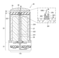
- FIG. 1 is a partial vertical cross-sectional view showing an example of a semiconductor structure of a photodetection device according to a first embodiment of the present disclosure.
- FIG. 2 is a diagram (part 1) showing an example of the manufacturing process of the uneven metal structure 26 according to the first embodiment.
- FIG. 2 is a diagram (Part 2) illustrating an example of the manufacturing process of the uneven metal structure 26 according to the first embodiment.
- FIG. 3 is a diagram (Part 3) illustrating an example of the manufacturing process of the uneven metal structure 26 according to the first embodiment.
- FIG. 1 is a block diagram illustrating an example of a schematic configuration of a photodetection device according to a first embodiment of the present disclosure.
- FIG. 1 is a partial vertical cross-sectional view showing an example of a semiconductor structure of a photodetection device according to a first embodiment of
- FIG. 4 is a diagram (part 4) illustrating an example of the manufacturing process of the uneven metal structure 26 according to the first embodiment.
- FIG. 5 is a diagram (Part 5) showing an example of the manufacturing process of the uneven metal structure 26 according to the first embodiment.
- FIG. 6 is a diagram (part 6) illustrating an example of the manufacturing process of the uneven metal structure 26 according to the first embodiment.
- FIG. 7 is a partial vertical cross-sectional view of a concavo-convex metal structure in a first modification of the first embodiment of the present disclosure.
- FIG. 7 is a partial vertical cross-sectional view of a concavo-convex metal structure in a second modification of the first embodiment of the present disclosure.
- FIG. 7 is a partial vertical cross-sectional view of a concavo-convex metal structure in a third modification of the first embodiment of the present disclosure.
- FIG. 7 is a partial vertical cross-sectional view of a concavo-convex metal structure in a fourth modification of the first embodiment of the present disclosure.
- FIG. 7 is a partial vertical cross-sectional view of the uneven metal structure in a fifth modification of the first embodiment of the present disclosure. It is a partial vertical cross-sectional view of the uneven metal structure in the 6th modification of the 1st embodiment of this indication.
- FIG. 7 is a plan view of a pixel in a photodetection device according to a second embodiment of the present disclosure.
- FIG. 7 is a plan view of a pixel in a photodetection device according to a third embodiment of the present disclosure.
- FIG. 7 is a plan view of a pixel in a photodetection device according to a fourth embodiment of the present disclosure.
- FIG. 7 is a plan view of a pixel in a photodetection device according to a fifth embodiment of the present disclosure.
- FIG. 7 is a plan view of a pixel in a photodetection device according to a sixth embodiment of the present disclosure.
- FIG. 7 is a plan view of a pixel in a photodetection device according to a seventh embodiment of the present disclosure.
- FIG. 7 is a plan view of a pixel in a photodetection device according to a seventh embodiment of the present disclosure.
- FIG. 7 is a plan view of a pixel in a photodetection device according to an eighth embodiment of the present disclosure.
- FIG. 7 is a characteristic diagram showing the absorption rate of each metal used in the uneven metal structure according to the ninth embodiment of the present disclosure.
- FIG. 9 is a characteristic diagram showing the wavelength dependence of the reflectance of rhodium used in the uneven metal structure according to the ninth embodiment of the present disclosure.
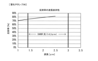
- FIG. 9 is a characteristic diagram showing the wavelength dependence of the reflectance of titanium nitride used in the uneven metal structure according to the ninth embodiment of the present disclosure. It is a partial vertical cross-sectional view of a photodetection device 1H according to a tenth embodiment of the present disclosure.
- FIG. 7 is a partial vertical cross-sectional view of a photodetection device according to a comparative example of the tenth embodiment.
- FIG. 7 is a plan view of an optical black pixel in a photodetection device according to a first modification of the tenth embodiment of the present disclosure.
- FIG. 7 is a plan view of an optical black pixel in a photodetection device according to a second modification of the tenth embodiment of the present disclosure.
- FIG. 1 is a block diagram illustrating a configuration example of an imaging device as an electronic device to which the present technology is applied.
- 1 is a block diagram illustrating a schematic configuration example of a vehicle control system, which is an example of a mobile body control system to which the technology according to the present disclosure can be applied.
- 26 is a diagram showing an example of the installation position of the imaging unit shown in FIG. 25.
- FIG. 25 is a diagram showing an example of the installation position of the imaging unit shown in FIG. 25.
- the "first conductivity type” is either p-type or n-type
- the “second conductivity type” means one of p-type or n-type, which is different from the “first conductivity type”.
- “+” and “-” appended to "n” and “p” refer to semiconductors with relatively high or low impurity density, respectively, compared to semiconductor regions without "+” and “-”. It means a territory. However, even if semiconductor regions are given the same "n” and "n”, this does not mean that the impurity density of each semiconductor region is strictly the same.
- FIG. 1 is a block diagram illustrating an example of a schematic configuration of a photodetection device according to a first embodiment of the present disclosure.
- the photodetector 1 uses a photoelectric conversion element such as a photodiode constituting each pixel to convert the amount of charge corresponding to the intensity of light imaged onto the pixel into an electrical signal, and outputs this as image data. It is a semiconductor device configured as a CMOS image sensor, for example.
- the photodetector 1 may be configured integrally as a system-on-chip (SoC) such as a CMOS LSI, but the following components may also be configured as separate LSIs, for example. .
- SoC system-on-chip
- the photodetection device 1 includes, for example, a pixel array section 11, a vertical drive section 12, a column processing section 13, a horizontal drive section 14, a system control section 15, and a signal processing section 16. , and includes components such as a data storage section 17.
- the pixel array section 11 includes a group of photoelectric conversion elements such as photodiodes that constitute the pixels 110 arranged in an array in the horizontal direction (row direction) and the vertical direction (column direction).
- the pixel array section 11 converts the amount of charge corresponding to the intensity of the incident light imaged onto each pixel 110 into an electrical signal, and outputs it as a pixel signal.
- the pixel array section 11 may include, for example, effective pixels arranged in a region that can receive actual light and dummy pixels arranged outside the region and shielded by metal or the like. Note that optical system elements such as a micro-on-chip lens and a color filter for condensing incident light are formed on each pixel 110 of the pixel array section 11 (not shown).
- the vertical drive section 12 includes a shift register, an address decoder, etc.
- the vertical drive section 12 drives each pixel 110 of the pixel array section 11, for example, simultaneously or in row units by supplying drive signals and the like to each pixel 110 via a plurality of pixel drive lines 18.
- the column processing section 13 reads out pixel signals from each pixel via the vertical signal line (VSL) 19 for each pixel row (column) of the pixel array section 11, and performs noise removal processing, correlated double sampling (CDS) processing, and A/D (Analog-to-Digital) conversion processing.
- the pixel signals processed by the column processing section 13 are output to the signal processing section 16.
- the horizontal drive section 14 includes a shift register, an address decoder, etc.
- the horizontal drive unit 14 sequentially selects pixels 110 corresponding to the pixel columns of the column processing unit 13. By this selective scanning by the horizontal driving section 14, pixel signals subjected to signal processing for each pixel 110 in the column processing section 13 are sequentially output to the signal processing section 16.
- the system control unit 15 includes a timing generator and the like that generate various timing signals.
- the system control unit 15 controls the vertical drive unit 12, the column processing unit 13, and the horizontal drive unit 14 based on a timing signal generated by a timing generator (not shown), for example.
- the signal processing unit 16 performs signal processing such as arithmetic processing on the pixel signals supplied from the column processing unit 13 while temporarily storing data in the data storage unit 17 as necessary, and adds data to each pixel signal. Outputs an image signal based on the Further, the signal processing unit 16 performs signal processing according to the flag output from the column processing unit 13.
- the photodetection device 1 to which the present technology is applied is not limited to the configuration described above.
- the data storage section 17 is arranged after the column processing section 13, and the pixel signal output from the column processing section 13 is supplied to the signal processing section 16 via the data storage section 17. It may be configured as follows.
- the photodetecting device 1 may be configured such that the column processing section 13, data storage section 17, and signal processing section 16 connected in series process each pixel signal in parallel.
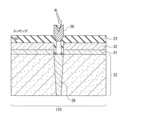
- FIG. 2 is a partial vertical cross-sectional view showing an example of the semiconductor structure of the photodetecting device 1 according to the first embodiment of the present disclosure.
- the semiconductor structure 20 schematically includes, for example, a wiring layer 21, a semiconductor layer 22, an interlayer film 23, a color filter 24, and an on-chip lens 25.
- the semiconductor structure 20 of the present disclosure also includes a textured metal structure 26 .
- Such a semiconductor structure 20 is constructed by, for example, integrally bonding a first silicon substrate including a wiring layer 21 and various logic circuits (not shown) and a second silicon substrate including a semiconductor layer 22. can be done.
- the on-chip lens 25 is an optical lens that efficiently condenses light that enters the photodetector 1 from the outside and forms an image on each pixel 110 of the semiconductor layer 22.
- On-chip lens 25 is typically arranged for each pixel 110.
- the on-chip lens 25 is formed of, for example, silicon oxide, silicon nitride, silicon oxynitride, organic SOG, polyimide resin, fluorine resin, or the like.
- the color filter 24 is an optical filter that selectively transmits light of a predetermined wavelength out of the light collected by the on-chip lens 25.
- four color filters 24 are used that selectively transmit wavelengths of red light, green light, blue light, and near-infrared light, but the present invention is not limited to this.
- a color filter 24 corresponding to any color (wavelength) is arranged in each pixel 110.
- the semiconductor layer 22 is a functional layer in which a group of pixel circuits including photoelectric conversion units 221 and 222 such as photodiodes that constitute each pixel 110 and electronic elements such as various transistors are formed.
- Each photoelectric conversion section 221, 222 of the semiconductor layer 22 generates an amount of charge according to the intensity of light incident through the on-chip lens 25 and color filter 24, converts this into an electric signal, and outputs it as a pixel signal. Output.
- Each photoelectric conversion section 221, 222 is an n-type region. Note that a part of the light (for example, near-infrared light, etc.) that has entered the incident surface of the semiconductor layer 22 can pass through the surface (that is, the front surface) opposite to the incident surface (that is, the back surface).
- the semiconductor layer 22 is manufactured on a silicon substrate by a semiconductor manufacturing process.
- the photoelectric conversion units 221 and 222 and various electronic elements are electrically connected to predetermined metal wiring in the wiring layer 21.
- an inter-pixel isolation section 27 that isolates each pixel 110 from each other may be formed in the semiconductor layer 22 .
- the inter-pixel isolation section 27 has a trench structure formed by etching, for example.
- the inter-pixel separation unit 27 prevents light incident on a pixel 110 from entering an adjacent pixel 110.
- an intra-pixel separation section 28 that separates the pixel 110 into two or more plurality may be formed in the semiconductor layer 22.
- the intra-pixel isolation section 28 has a trench structure formed by etching, for example, and prevents light incident on the pixel 110 from entering the adjacent photoelectric conversion sections 221 and 222.
- a p-type region 223 is formed between the photoelectric conversion section 221 and the inter-pixel isolation section 27 and the intra-pixel isolation section 28 .
- a p-type region 224 is formed between the photoelectric conversion section 222 and the inter-pixel isolation section 27 and the intra-pixel isolation section 28 .
- the wiring layer 21 is a layer in which a metal wiring pattern is formed for transmitting power and various drive signals to each pixel 110 in the semiconductor layer 22 and for transmitting pixel signals read out from each pixel 110.
- the wiring layer 21 may typically be configured by stacking a plurality of metal wiring pattern layers with an interlayer insulating film interposed therebetween. Furthermore, the laminated metal wiring patterns are electrically connected, for example, via vias, if necessary.
- the wiring layer 21 is formed of a metal such as aluminum (Al) or copper (Cu), for example.
- the interlayer insulating film is formed of silicon oxide or the like, for example.
- the uneven metal structure 26 is a structure that is disposed on the light incident surface (back surface) side of the intra-pixel separation section 28 in the interlayer film 23 and has predetermined reflection or absorption characteristics for visible light.
- the textured metal structure 26 is made of tungsten and reflects or absorbs light incident on the pixel 110 multiple times. Tungsten has a property of 50% absorption/50% reflection in visible light.
- the uneven metal structure 26 has a bottom portion 261 arranged parallel to the light incident surface of the semiconductor layer 22 and at least two protrusions 262 in a direction perpendicular to the extending direction of the bottom portion 261. , 100% of the light incident through the on-chip lens 25 is reflected or absorbed by the protrusion 262 to become 50% light, and reflected or absorbed by the bottom part 261 to become 25% light and reflected. .
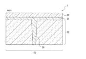
- FIGS. 3A to 3F are diagrams showing an example of the manufacturing process of the uneven metal structure 26 according to the first embodiment.
- an intra-pixel isolation section 28 is formed by digging into the semiconductor layer 22.
- FIG. A p-type pinning film 31 is laminated on the light incidence surface (back surface) side of the semiconductor layer 22, and a pinning film 31 is laminated on the light incidence surface (back surface) side of the p-type pinning film 31.
- Connected n-type layers 32 are stacked.
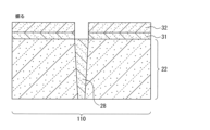
- FIG. 3B the light incident surface side of the intra-pixel separation section 28 is carved.
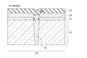
- an interlayer film 23 made of silicon oxide is formed on the light incident surface side of the n-type layer 32, and the dug portion of the intra-pixel isolation section 28 is backfilled with the interlayer film 23.
- a metal film 33 such as tungsten is formed on the light incident surface side of the interlayer film 23 by CVD growth, and in FIG. A resist film 34 is formed on the surface side, and in FIG. 3F, the resist film 34 is removed by etching to form an uneven metal structure 26 on the light incident surface side of the interlayer film 23.
- the uneven metal structure 26 is installed on the light incident surface side of the intra-pixel separation section 28, and the uneven metal structure 26 allows the light to enter through the on-chip lens 25. Suppresses unnecessary light by reflecting or absorbing light. In the uneven metal structure 26, by utilizing the characteristic of tungsten of 50% absorption/50% reflection in visible light, it is reflected or absorbed multiple times to cut unnecessary light components by 50% or more, thereby improving color mixture. Connect.
- FIG. 4 is a partial vertical cross-sectional view of the uneven metal structure 26A in a first modification of the first embodiment of the present disclosure.
- a plurality of protrusions 262 protrude from the bottom side 261 of the uneven metal structure 26A, and an acute angle portion 263 is formed at the tip of each of the plurality of protrusions 262.
- the acute angle portions 263 can guide light between the plurality of protrusions 262 and increase the number of reflections or absorptions, thereby improving color mixing.
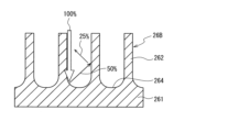
- FIG. 5 is a partial vertical cross-sectional view of the uneven metal structure 26B in a second modification of the first embodiment of the present disclosure.
- a rounded portion 264 is formed between a plurality of (only four are shown in FIG. 5) protrusions 262 on the bottom side 261 of the uneven metal structure 26B.
- the rounded portion 264 of the bottom portion 261 can increase the number of reflections or absorptions, thereby improving color mixing.
- FIG. 6 is a partial vertical cross-sectional view of a concavo-convex metal structure 26C in a third modification of the first embodiment of the present disclosure.
- An antireflection film 41 made of an insulator is coated on the bottom portion 261 and a plurality of (only four are shown in FIG. 6) protrusions 262 of the uneven metal structure 26C.
- the antireflection film 41 can reduce the reflectance of light and further improve color mixture.
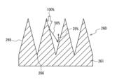
- FIG. 7 is a partial vertical cross-sectional view of an uneven metal structure 26D in a fourth modification of the first embodiment of the present disclosure.
- the same parts as those in FIG. 2 are given the same reference numerals and detailed explanations will be omitted.
- a plurality of (only four are shown in FIG. 7) protrusions 265 each having an acute angle are formed on the bottom side 261 of the uneven metal structure 26D.
- an acute angle portion 266 is formed between the plurality of protrusions 265.
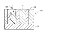
- FIG. 8 is a partial vertical cross-sectional view of an uneven metal structure 26E in a fifth modification of the first embodiment of the present disclosure.
- a low refractive material 42 is filled between the bottom portion 261 and each of the plurality of (three shown in FIG. 8) protrusions 262.
- the low refractive material 42 has a lower refractive index than the on-chip lens 25, for example. Therefore, by filling the spaces between the plurality of protrusions 262 with a low refractive material 42 having a refractive index lower than that of the incident region, light can be confined, thereby improving color mixture.
- FIG. 9 is a partial vertical cross-sectional view of a concavo-convex metal structure 26F in a sixth modification of the first embodiment of the present disclosure.
- the uneven metal structure 26F is arranged within the interlayer film 23.
- a high refractive material 43 is applied between the color filter 24 and the interlayer film 23 .
- High refractive material 43 has a higher refractive index than interlayer film 23. Therefore, by applying a high refractive material 43 having a higher refractive index than the interlayer film 23 on which the uneven metal structure 26F is arranged under the color filter 24, light can be confined in the self-pixel 110. This makes it possible to improve color mixture.
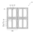
- FIG. 10 is a plan view of a pixel 110A in a photodetection device 1A according to a second embodiment of the present disclosure.
- the uneven metal structure 51 is arranged between the intra-pixel separation section 28 and the on-chip lens 25.
- a concavo-convex metal structure 52 is arranged between the inter-pixel separation section 27 and the on-chip lens 25.
- the uneven metal structure 51 is formed by a bottom side 511 and a plurality of protrusions 512 extending from the bottom side 511 toward the on-chip lens 25 .
- the plurality of protrusions 512 are rectangular in plan view (row direction or column direction). Further, the uneven metal structure 52 is formed of a bottom side 521 and a plurality of protrusions 522 in a direction from the bottom side 521 toward the on-chip lens 25 . The plurality of protrusions 522 are rectangular in plan view (row direction or column direction).
- FIG. 11 is a plan view of a pixel 110B in a photodetection device 1B according to a third embodiment of the present disclosure.
- the plurality of protrusions 513 of the uneven metal structure 51 in the third embodiment of the present disclosure are circular in plan view (row direction or column direction). Further, the plurality of protrusions 523 of the uneven metal structure 52 are round in plan view (row direction or column direction).
- FIG. 12 is a plan view of a pixel 110C in a photodetection device 1C according to the fourth embodiment of the present disclosure.
- the plurality of protrusions 514 of the uneven metal structure 51 in the fourth embodiment of the present disclosure are slits in plan view (row direction or column direction).
- the plurality of protrusions 524 of the uneven metal structure 52 are slits in plan view (row direction or column direction).
- FIG. 13 is a plan view of pixels 110D1 and 110D2 in photodetection device 1D according to the fifth embodiment of the present disclosure.
- the same parts as those in FIG. 10 are given the same reference numerals and detailed explanations will be omitted.
- Half of the pixel 110D1 is covered with the uneven metal structure 61.
- Half of the pixel 110D2 is covered with the uneven metal structure 62.
- a problem may occur in which light is reflected by a half-open metal and leaks to adjacent pixels.
- the pixel 110D2 a problem may occur in which light is reflected by a half-open metal and leaks to adjacent pixels. Therefore, in the fifth embodiment of the present disclosure, the uneven metal structures 61 and 62 are arranged in a half-open metal.
- FIG. 14 is a plan view of a pixel 110E in a photodetection device 1E according to a sixth embodiment of the present disclosure.
- the pixel 110E in the sixth embodiment of the present disclosure has two photoelectric conversion units 221 and 222 arranged in two rows and one column for the on-chip lens 25.
- An uneven metal structure 71 is arranged in the intra-pixel separation section 28, and an uneven metal structure 72 is arranged in the inter-pixel separation section 27.
- the uneven metal structure 71 is formed by a bottom side 711 and a plurality of protrusions 712 extending from the bottom side 711 toward the on-chip lens 25 .
- the plurality of protrusions 712 are circular in plan view (row direction or column direction).
- the uneven metal structure 72 is formed by a bottom side 721 and a plurality of protrusions 722 extending from the bottom side 721 toward the on-chip lens 25 .
- the plurality of protrusions 722 are circular in plan view (row direction or column direction).
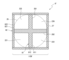
- FIG. 15 is a plan view of a pixel 110F in a photodetection device 1F according to a seventh embodiment of the present disclosure.
- the pixel 110F in the seventh embodiment of the present disclosure has four photoelectric conversion units 221, 222, 225, and 226 arranged in 2 rows and 2 columns for the on-chip lens 25.
- the four photoelectric conversion units 221, 222, 225, and 226 are separated by intra-pixel separation units 281 and 282.
- An uneven metal structure 81 is arranged in the intra-pixel separation parts 281 and 282, and an uneven metal structure 82 is arranged in the inter-pixel separation part 27.
- the uneven metal structure 81 is formed by a bottom side 811 and a plurality of protrusions 812 extending from the bottom side 811 toward the on-chip lens 25 .
- the plurality of protrusions 812 are circular in plan view (row direction or column direction).
- the uneven metal structure 82 is formed by a bottom side 821 and a plurality of protrusions 822 extending from the bottom side 821 toward the on-chip lens 25 .
- the plurality of protrusions 822 are circular in plan view (row direction or column direction).
- FIG. 16 is a plan view of a pixel 110G in a photodetection device 1G according to the eighth embodiment of the present disclosure.
- a concavo-convex metal structure 91 is arranged in the intra-pixel separation section 28, and a concave-convex metal structure 92 is arranged in the inter-pixel separation section 27.
- the uneven metal structure 91 is formed of a bottom side 911 and a plurality of protrusions 912 extending from the bottom side 911 toward the on-chip lens 25 .
- the plurality of protrusions 912 are circular in plan view (row direction or column direction).
- the uneven metal structure 92 is formed by a bottom side 921 and a plurality of protrusions 922 extending from the bottom side 921 toward the on-chip lens 25 .
- the plurality of protrusions 922 are circular in plan view (row direction or column direction).
- an uneven metal structure 93 is provided on the side wall of the inter-pixel separation section 27.
- FIG. 17 is a characteristic diagram showing the absorption rate of each metal used in the uneven metal structure in the ninth embodiment of the present disclosure.
- tungsten 101 has an absorption rate of 50% in the visible light region.
- Iron 102 has a certain percentage of absorption in the visible light region.
- Copper 103, aluminum 104, and silver 105 also have a certain rate of absorption in the visible light region. Therefore, iron 102, copper 103, aluminum 104, and silver 105 can be used as substitute materials for tungsten 101 in visible light.
- rhodium shown in FIG. 18 and titanium nitride shown in FIG. 19 are suitable materials.
- FIG. 20 is a partial vertical cross-sectional view of a photodetecting device 1H according to a tenth embodiment of the present disclosure.
- the photodetector 1H has a photoelectric conversion board section 200.
- the photoelectric conversion substrate section 200 includes a first compound semiconductor layer 201 and a second compound semiconductor layer 202 disposed on the light incident surface side of the first compound semiconductor layer 201.
- a recombination prevention layer 203 as a second compound semiconductor layer is provided on the light incident surface side of the second compound semiconductor layer 202.
- Each of the first compound semiconductor layer 201, the second compound semiconductor layer 202, and the recombination prevention layer 203 is provided in common to each optical black pixel 300.
- the above-described photoelectric conversion element 204 is provided for each optical black pixel 300.
- the recombination prevention layer 203 suppresses dark current generation.
- a transparent electrode 205 is arranged on the light incident surface side of the recombination prevention layer 203.
- the transparent electrode 205 is in contact with and electrically connected to the recombination prevention layer 203.
- a predetermined bias voltage is applied to the transparent electrode 205.
- a material that can transmit infrared light and visible light such as ITO (Indium Tin Oxide), can be used.
- the uneven metal structure 400 is arranged on the light incident surface side of the transparent electrode 205.
- a plurality of (only four are shown in FIG. 20) protrusions 402 protrude from a bottom side 401.
- FIG. 21 is a partial vertical cross-sectional view of a photodetector 1H1 according to a comparative example of the tenth embodiment.
- a passivation layer 206 is arranged on the light incident surface side of the transparent electrode 205.
- a material that can transmit infrared light and visible light such as silicon oxide (SiO2), silicon nitride (SiN), or aluminum oxide (Al2O3), can be used.
- a light-shielding metal 500 is placed on the light incident surface side of the passivation layer 206. Since the light-shielding metal 500 directly reflects the light incident through the on-chip lens 25, light reflected by other normal pixels may enter the light-shielding metal 500.
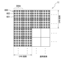
- FIG. 22 is a plan view of an optical black pixel 300A in a photodetector 1I according to a first modification of the tenth embodiment of the present disclosure.
- the uneven metal structure 600 is arranged between the optical black pixel 300A and the on-chip lens 25.
- the uneven metal structure 600 is formed by a bottom side 601 and a plurality of protrusions 602 extending from the bottom side 601 toward the on-chip lens 25 .
- the plurality of protrusions 602 are rectangular in plan view (row direction or column direction).
- FIG. 23 is a plan view of an optical black pixel 300B in a photodetector 1J according to a second modification of the tenth embodiment of the present disclosure.
- the uneven metal structure 700 is arranged between the optical black pixel 300B and the on-chip lens 25.
- the uneven metal structure 700 is formed by a bottom side 701 and a plurality of protrusions 702 extending from the bottom side 701 toward the on-chip lens 25 .
- the plurality of protrusions 702 are slits in plan view (row direction or column direction).
- the present technology is applicable to the first to tenth embodiments, the first to sixth modified examples of the first embodiment, the first modified example and the second modified example of the tenth embodiment.
- the discussion and drawings that form part of this disclosure should not be understood as limiting the present technology.
- the first to tenth embodiments, the first to sixth modifications of the first embodiment, and the first modification and second modification of the tenth embodiment are disclosed, respectively.
- the configurations can be combined as appropriate to the extent that no contradiction occurs. For example, configurations disclosed by a plurality of different embodiments may be combined, or configurations disclosed by a plurality of different modifications of the same embodiment may be combined.
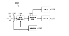
- FIG. 24 is a block diagram showing a configuration example of an imaging device as an electronic device to which the present technology is applied.
- the imaging device 2201 shown in FIG. 24 includes an optical system 2202, a shutter device 2203, a solid-state image sensor 2204 as a photodetector, a control circuit 2205, a signal processing circuit 2206, a monitor 2207, and two memories 2208. Capable of capturing still images and moving images.
- the optical system 2202 includes one or more lenses, guides light (incident light) from a subject to the solid-state image sensor 2204, and forms an image on the light-receiving surface of the solid-state image sensor 2204.
- the shutter device 2203 is disposed between the optical system 2202 and the solid-state image sensor 2204, and controls the light irradiation period and the light shielding period to the solid-state image sensor 2204 under the control of the control circuit 2205.
- the solid-state image sensor 2204 is configured by a package containing the above-described solid-state image sensor.
- the solid-state image sensor 2204 accumulates signal charges for a certain period of time according to the light that is imaged on the light receiving surface via the optical system 2202 and the shutter device 2203.
- the signal charge accumulated in the solid-state image sensor 2204 is transferred according to a drive signal (timing signal) supplied from the control circuit 2205.
- the control circuit 2205 outputs a drive signal that controls the transfer operation of the solid-state image sensor 2204 and the shutter operation of the shutter device 2203, and drives the solid-state image sensor 2204 and the shutter device 2203.
- the signal processing circuit 2206 performs various signal processing on the signal charges output from the solid-state image sensor 2204.
- An image (image data) obtained by signal processing by the signal processing circuit 2206 is supplied to a monitor 2207 and displayed, or supplied to a memory 2208 and stored (recorded).
- the photodetecting devices 1, 1A, 1B, 1C, 1D, 1E, 1F, 1G, 1H, 1I, 1J are applied instead of the solid-state imaging device 2204 described above. becomes possible.
- the technology according to the present disclosure (this technology) can be applied to various products.
- the technology according to the present disclosure may be realized as a device mounted on any type of moving body such as a car, electric vehicle, hybrid electric vehicle, motorcycle, bicycle, personal mobility, airplane, drone, ship, robot, etc. It's okay.
- FIG. 25 is a block diagram illustrating a schematic configuration example of a vehicle control system, which is an example of a mobile body control system to which the technology according to the present disclosure can be applied.
- Vehicle control system 12000 includes a plurality of electronic control units connected via communication network 12001.
- the vehicle control system 12000 includes a drive system control unit 12010, a body system control unit 12020, an outside vehicle information detection unit 12030, an inside vehicle information detection unit 12040, and an integrated control unit 12050.
- a microcomputer 12051, an audio/image output section 12052, and an in-vehicle network I/F (interface) 12053 are illustrated.
- the drive system control unit 12010 controls the operation of devices related to the drive system of the vehicle according to various programs.
- the drive system control unit 12010 includes a drive force generation device such as an internal combustion engine or a drive motor that generates drive force for the vehicle, a drive force transmission mechanism that transmits the drive force to wheels, and a drive force transmission mechanism that controls the steering angle of the vehicle. It functions as a control device for a steering mechanism to adjust and a braking device to generate braking force for the vehicle.
- the body system control unit 12020 controls the operations of various devices installed in the vehicle body according to various programs.
- the body system control unit 12020 functions as a keyless entry system, a smart key system, a power window device, or a control device for various lamps such as a headlamp, a back lamp, a brake lamp, a turn signal, or a fog lamp.
- radio waves transmitted from a portable device that replaces a key or signals from various switches may be input to the body control unit 12020.
- the body system control unit 12020 receives input of these radio waves or signals, and controls the door lock device, power window device, lamp, etc. of the vehicle.
- the external information detection unit 12030 detects information external to the vehicle in which the vehicle control system 12000 is mounted.
- an imaging section 12031 is connected to the outside-vehicle information detection unit 12030.
- the vehicle exterior information detection unit 12030 causes the imaging unit 12031 to capture an image of the exterior of the vehicle, and receives the captured image.
- the external information detection unit 12030 may perform object detection processing such as a person, car, obstacle, sign, or text on the road surface or distance detection processing based on the received image.
- the imaging unit 12031 is an optical sensor that receives light and outputs an electrical signal according to the amount of received light.
- the imaging unit 12031 can output the electrical signal as an image or as distance measurement information.
- the light received by the imaging unit 12031 may be visible light or non-visible light such as infrared rays.
- the in-vehicle information detection unit 12040 detects in-vehicle information.
- a driver condition detection section 12041 that detects the condition of the driver is connected to the in-vehicle information detection unit 12040.
- the driver condition detection unit 12041 includes, for example, a camera that images the driver, and the in-vehicle information detection unit 12040 detects the degree of fatigue or concentration of the driver based on the detection information input from the driver condition detection unit 12041. It may be calculated, or it may be determined whether the driver is falling asleep.
- the microcomputer 12051 calculates control target values for the driving force generation device, steering mechanism, or braking device based on the information inside and outside the vehicle acquired by the vehicle exterior information detection unit 12030 or the vehicle interior information detection unit 12040, Control commands can be output to 12010.
- the microcomputer 12051 realizes ADAS (Advanced Driver Assistance System) functions, including vehicle collision avoidance or impact mitigation, following distance based on vehicle distance, vehicle speed maintenance, vehicle collision warning, vehicle lane departure warning, etc. It is possible to perform cooperative control for the purpose of ADAS (Advanced Driver Assistance System) functions, including vehicle collision avoidance or impact mitigation, following distance based on vehicle distance, vehicle speed maintenance, vehicle collision warning, vehicle lane departure warning, etc. It is possible to perform cooperative control for the purpose of
- ADAS Advanced Driver Assistance System
- the microcomputer 12051 controls the driving force generating device, steering mechanism, braking device, etc. based on information about the surroundings of the vehicle acquired by the vehicle exterior information detection unit 12030 or the vehicle interior information detection unit 12040. It is possible to perform cooperative control for the purpose of autonomous driving, etc., which does not rely on operation.
- the microcomputer 12051 can output a control command to the body system control unit 12020 based on the information outside the vehicle acquired by the outside information detection unit 12030.
- the microcomputer 12051 controls the headlamps according to the position of the preceding vehicle or oncoming vehicle detected by the vehicle exterior information detection unit 12030, and performs cooperative control for the purpose of preventing glare, such as switching from high beam to low beam. It can be carried out.
- the audio and image output unit 12052 transmits an output signal of at least one of audio and images to an output device that can visually or audibly notify information to the occupants of the vehicle or to the outside of the vehicle.
- an audio speaker 12061, a display section 12062, and an instrument panel 12063 are illustrated as output devices.
- the display unit 12062 may include, for example, at least one of an on-board display and a head-up display.
- FIG. 26 is a diagram showing an example of the installation position of the imaging section 12031.
- vehicle 12100 includes imaging units 12101 , 12102 , 12103 , 12104 , and 12105 as imaging unit 12031 .
- the imaging units 12101, 12102, 12103, 12104, and 12105 are provided, for example, at positions such as the front nose, side mirrors, rear bumper, back door, and the top of the windshield inside the vehicle 12100.
- An imaging unit 12101 provided in the front nose and an imaging unit 12105 provided above the windshield inside the vehicle mainly acquire images in front of the vehicle 12100.
- Imaging units 12102 and 12103 provided in the side mirrors mainly capture images of the sides of the vehicle 12100.
- An imaging unit 12104 provided in the rear bumper or back door mainly captures images of the rear of the vehicle 12100.
- the images of the front acquired by the imaging units 12101 and 12105 are mainly used for detecting preceding vehicles, pedestrians, obstacles, traffic lights, traffic signs, lanes, and the like.
- FIG. 26 shows an example of the imaging range of the imaging units 12101 to 12104.
- An imaging range 12111 indicates the imaging range of the imaging unit 12101 provided on the front nose
- imaging ranges 12112 and 12113 indicate imaging ranges of the imaging units 12102 and 12103 provided on the side mirrors, respectively
- an imaging range 12114 shows the imaging range of the imaging unit 12101 provided on the front nose.
- the imaging range of the imaging unit 12104 provided in the rear bumper or back door is shown. For example, by overlapping the image data captured by the imaging units 12101 to 12104, an overhead image of the vehicle 12100 viewed from above can be obtained.
- At least one of the imaging units 12101 to 12104 may have a function of acquiring distance information.
- at least one of the imaging units 12101 to 12104 may be a stereo camera including a plurality of image sensors, or may be an image sensor having pixels for phase difference detection.
- the microcomputer 12051 determines the distance to each three-dimensional object within the imaging ranges 12111 to 12114 and the temporal change in this distance (relative speed with respect to the vehicle 12100) based on the distance information obtained from the imaging units 12101 to 12104. In particular, by determining the three-dimensional object that is closest to the vehicle 12100 on its path and that is traveling at a predetermined speed (for example, 0 km/h or more) in approximately the same direction as the vehicle 12100, it is possible to extract the three-dimensional object as the preceding vehicle. can.
- a predetermined speed for example, 0 km/h or more
- the microcomputer 12051 can set an inter-vehicle distance to be secured in advance in front of the preceding vehicle, and perform automatic brake control (including follow-up stop control), automatic acceleration control (including follow-up start control), and the like. In this way, it is possible to perform cooperative control for the purpose of autonomous driving, etc., in which the vehicle travels autonomously without depending on the driver's operation.
- the microcomputer 12051 transfers three-dimensional object data to other three-dimensional objects such as two-wheeled vehicles, regular vehicles, large vehicles, pedestrians, and utility poles based on the distance information obtained from the imaging units 12101 to 12104. It can be classified and extracted and used for automatic obstacle avoidance. For example, the microcomputer 12051 identifies obstacles around the vehicle 12100 into obstacles that are visible to the driver of the vehicle 12100 and obstacles that are difficult to see. Then, the microcomputer 12051 determines a collision risk indicating the degree of risk of collision with each obstacle, and when the collision risk exceeds a set value and there is a possibility of a collision, the microcomputer 12051 transmits information via the audio speaker 12061 and the display unit 12062. By outputting a warning to the driver via the vehicle control unit 12010 and performing forced deceleration and avoidance steering via the drive system control unit 12010, driving support for collision avoidance can be provided.
- the microcomputer 12051 determines a collision risk indicating the degree of risk of collision with each obstacle, and when the collision risk exceed
- At least one of the imaging units 12101 to 12104 may be an infrared camera that detects infrared rays.
- the microcomputer 12051 can recognize a pedestrian by determining whether the pedestrian is present in the images captured by the imaging units 12101 to 12104.
- pedestrian recognition involves, for example, a procedure for extracting feature points in images captured by the imaging units 12101 to 12104 as infrared cameras, and a pattern matching process is performed on a series of feature points indicating the outline of an object to determine whether it is a pedestrian or not.
- the audio image output unit 12052 creates a rectangular outline for emphasis on the recognized pedestrian.
- the display unit 12062 is controlled to display the .
- the audio image output unit 12052 may control the display unit 12062 to display an icon or the like indicating a pedestrian at a desired position.
- the present disclosure can also have the following configuration.
- a semiconductor layer in which a plurality of pixels capable of generating electrical signals in response to light incident from the outside are arranged in a matrix; an inter-pixel separation section formed in the semiconductor layer and insulating and blocking light between the adjacent pixels; an intra-pixel separation section formed in the semiconductor layer and separating the pixel into a plurality of parts; an on-chip lens disposed on the light incident surface side of the semiconductor layer and formed for each pixel;
- a photodetection device comprising: a concavo-convex metal structure disposed between the intra-pixel separation section and the on-chip lens, and having predetermined reflection characteristics or absorption characteristics with respect to visible light.
- the uneven metal structure has a bottom portion disposed parallel to the light incident surface of the semiconductor layer, and at least two or more protrusions in a direction perpendicular to the extending direction of the bottom portion, and has a plurality of protrusions.
- the photodetecting device according to (1) above which reflects or absorbs the light that has entered through the on-chip lens between the parts multiple times.
- the uneven metal structure includes a first refractive material filled between the bottom portion and each of the plurality of protrusions and having a lower refractive index than the material of the on-chip lens. Detection device.
- the uneven metal structure has a bottom portion arranged parallel to the light incident surface side of the inter-pixel separation portion and the intra-pixel separation portion, and at least two or more protrusions in a direction perpendicular to the extending direction of the bottom portion. and has a The photodetecting device according to (9) above, wherein the plurality of protrusions are round or rectangular in plan view.
- the uneven metal structure has a bottom portion arranged parallel to the light incident surface side of the inter-pixel separation portion and the intra-pixel separation portion, and at least two or more protrusions in a direction perpendicular to the extending direction of the bottom portion.
- the photodetection device according to (9) above has a The photodetection device according to (9) above, wherein the plurality of protrusions are slits in plan view.
- the photodetection device according to (1) above wherein at least a portion of the plurality of pixels covers half of the pixels with the uneven metal structure.
- the photodetection device according to (9) above, wherein at least some of the plurality of pixels have four photoelectric conversion units arranged in 2 rows and 2 columns with respect to the on-chip lens.
- the photodetecting device according to (1) above wherein the uneven metal structure is provided on a side wall of the inter-pixel separation section.
- the metal material of the uneven metal structure is selected from at least one of tungsten, iron, aluminum, copper, silver, rhodium, and titanium nitride.
- At least some of the plurality of pixels are optical black pixels, The photodetecting device according to (1) above, wherein the uneven metal structure is disposed on the light incident surface side of the optical black pixel.
- the uneven metal structure has a bottom portion arranged parallel to the light incident surface side of the optical black pixel, and at least two or more protruding portions in a direction perpendicular to the extending direction of the bottom portion, The photodetecting device according to (17) above, wherein the plurality of protrusions are round or rectangular in plan view.
- the uneven metal structure has a bottom portion arranged parallel to the light incident surface side of the optical black pixel, and at least two or more protruding portions in a direction perpendicular to the extending direction of the bottom portion, The photodetection device according to (17) above, wherein the plurality of protrusions are slits in plan view.
- a semiconductor layer in which a plurality of pixels capable of generating electrical signals in response to light incident from the outside are arranged in a matrix; an inter-pixel separation section formed in the semiconductor layer and insulating and blocking light between the adjacent pixels; an intra-pixel separation section formed in the semiconductor layer and separating the pixel into a plurality of parts; an on-chip lens disposed on the light incident surface side of the semiconductor layer and formed for each pixel;
- a photodetecting device comprising: a concave-convex metal structure disposed between the intra-pixel separation section and the on-chip lens and having predetermined reflection characteristics or absorption characteristics with respect to visible light; Electronics.
- Pixel array section 12 Vertical drive section 13 Column processing section 14 Horizontal drive section 15 System control section 16 Signal processing section 17 Data storage section 18 Pixel drive line 19 Vertical signal line (VSL) 20 Semiconductor structure 21 Wiring layer 22 Semiconductor layer 23 Interlayer film 24 Color filter 25 On-chip lens 26, 26A, 26B, 26C, 26D, 26E, 26F, 51, 52, 61, 62, 71, 72, 81, 82, 91 , 92, 93 Uneven metal structure 27 Inter-pixel isolation section 28, 281, 282 Intra-pixel isolation section 31 Pinning film 32 N-type layer 33 Metal film 34 Resist film 41 Anti-reflection film 42 Low refractive material 43 High refractive material 101 Tungsten 102 Iron 103 Copper 104 Aluminum 105 Silver 110, 110A, 110B, 110C, 110D1, 110D2, 110E, 110F, 110G Pixel 200
Landscapes
- Physics & Mathematics (AREA)
- Engineering & Computer Science (AREA)
- Multimedia (AREA)
- Signal Processing (AREA)
- General Physics & Mathematics (AREA)
- Electromagnetism (AREA)
- Radar, Positioning & Navigation (AREA)
- Remote Sensing (AREA)
- Optics & Photonics (AREA)
- Solid State Image Pick-Up Elements (AREA)
- Transforming Light Signals Into Electric Signals (AREA)
Abstract
複数のフォトダイオードを有する画素において、混色を改善することが可能な光検出装置を提供する。光検出装置は、半導体層と、画素間分離部と、画素内分離部と、オンチップレンズと、凹凸金属構造体とを備える。半導体層は、外部から入射した光に応じて電気信号を生成可能な複数の画素が行列状に配置される。画素間分離部は、半導体層に形成され、隣接する画素の間を絶縁して遮光する。画素内分離部は、半導体層に形成され、画素を複数に分離する。オンチップレンズは、半導体層の光入射面側に配置され、画素ごとに形成される。凹凸金属構造体は、画素内分離部とオンチップレンズとの間に配置され、可視光に対し所定の反射特性または吸収特性を有する。
Description
本開示に係る技術(本技術)は、光検出装置、及び光検出装置を備える電子機器に関する。
従来、デジタルスチルカメラやデジタルビデオカメラなどの撮像機能を備えた電子機器においては、光検出装置として、例えば、CCD(Charge Coupled Device)やCMOS(Complementary Metal Oxide Semiconductor)イメージセンサなどの固体撮像素子が使用されている。光検出装置は、光電変換を行うフォトダイオード(光電変換素子)とトランジスタとが組み合わされた画素を有しており、平面的に配置された複数の画素から出力される画素信号に基づいて画像が構築される。
例えば、固体撮像素子では、フォトダイオードに蓄積された電荷が、フォトダイオードと増幅トランジスタのゲート電極との接続部に設けられる所定の容量を有するFD(フローティングディフュージョン)部に転送される。そして、FD部に蓄積された電荷の量に応じた画素信号が画素から読み出され、コンパレータを有するAD(Analog Digital)変換回路によってAD変換されて出力される。
また、近年、CMOSイメージセンサの画素の一部を使用して位相を検出し、AF(オートフォーカス)速度を向上させる技術、いわゆる像面位相差AFが普及している。像面位相差AFでは、画素が有するフォトダイオードが複数に分割され、分割された各フォトダイオードにより得られる画素信号に基づいて位相情報が生成され、その位相情報に基づいて測距が行われる。
ところで、光が斜めに入射すると、画素に配置されたカラーフィルタが透過させる入射光とは異なる波長の入射光が混入し、混色が生じる場合がある。この場合、隣接するフォトダイオードの出力に差分が生じやすい。
下記特許文献1では、隣接する第1の画素のカラーフィルタと第2の画素のカラーフィルタとの間に画素間壁を設け、画素間壁をカラーフィルタとフォトダイオードとの間の層間膜内部まで延伸させ、画素間壁により混色を防ぐ撮像装置が提案されている。
下記特許文献1では、隣接する第1の画素のカラーフィルタと第2の画素のカラーフィルタとの間に画素間壁を設け、画素間壁をカラーフィルタとフォトダイオードとの間の層間膜内部まで延伸させ、画素間壁により混色を防ぐ撮像装置が提案されている。
ところで、上記特許文献1に開示される技術は、隣接する画素間で混色を防ぐ技術であり、1つの画素内で分割された複数のフォトダイオード間で混色を防ぐ技術ではない。
本開示はこのような事情に鑑みてなされたもので、複数のフォトダイオードを有する画素において、混色を改善することが可能な光検出装置及び電子機器を提供することを目的とする。
本開示の一態様は、外部から入射した光に応じて電気信号を生成可能な複数の画素が行列状に配置された半導体層と、前記半導体層に形成され、隣接する前記画素の間を絶縁して遮光する画素間分離部と、前記半導体層に形成され、前記画素を複数に分離する画素内分離部と、前記半導体層の前記光入射面側に配置され、前記画素ごとに形成されたオンチップレンズと、前記画素内分離部と前記オンチップレンズとの間に配置され、可視光に対し所定の反射特性または吸収特性を有する凹凸金属構造体と、を備える、光検出装置である。
本開示の他の態様は、外部から入射した光に応じて電気信号を生成可能な複数の画素が行列状に配置された半導体層と、前記半導体層に形成され、隣接する前記画素の間を絶縁して遮光する画素間分離部と、前記半導体層に形成され、前記画素を複数に分離する画素内分離部と、前記半導体層の前記光入射面側に配置され、前記画素ごとに形成されたオンチップレンズと、前記画素内分離部と前記オンチップレンズとの間に配置され、可視光に対し所定の反射特性または吸収特性を有する凹凸金属構造体と、を備える光検出装置を備えた、電子機器である。
以下において、図面を参照して本開示の実施形態を説明する。以下の説明で参照する図面の記載において、同一又は類似の部分には同一又は類似の符号を付し、重複する説明を省略する。但し、図面は模式的なものであり、厚みと平面寸法との関係、各装置や各部材の厚みの比率等は現実のものと異なることに留意すべきである。したがって、具体的な厚みや寸法は以下の説明を参酌して判定すべきものである。また、図面相互間においても互いの寸法の関係や比率が異なる部分が含まれていることは勿論である。
本明細書において、「第1導電型」はp型又はn型の一方であり、「第2導電型」はp型又はn型のうちの「第1導電型」とは異なる一方を意味する。また、「n」や「p」に付す「+」や「-」は、「+」及び「-」が付記されていない半導体領域に比して、それぞれ相対的に不純物密度が高い又は低い半導体領域であることを意味する。但し、同じ「n」と「n」とが付された半導体領域であっても、それぞれの半導体領域の不純物密度が厳密に同じであることを意味するものではない。
また、以下の説明における上下等の方向の定義は、単に説明の便宜上の定義であって、本開示の技術的思想を限定するものではない。例えば、対象を90°回転して観察すれば上下は左右に変換して読まれ、180°回転して観察すれば上下は反転して読まれることは勿論である。
なお、本明細書中に記載される効果はあくまで例示であって限定されるものでは無く、また他の効果があってもよい。
なお、本明細書中に記載される効果はあくまで例示であって限定されるものでは無く、また他の効果があってもよい。
<第1の実施形態>
(光検出装置の全体構成)
図1は、本開示の第1の実施形態に係る光検出装置の概略的構成の一例を示すブロック図である。光検出装置1は、各画素を構成するフォトダイオード等の光電変換素子を用いて、該画素上に結像した光の強弱に応じた電荷量を電気信号に変換し、これを画像データとして出力する半導体装置であり、例えばCMOSイメージセンサとして構成される。光検出装置1は、例えば、CMOS LSIのようなシステム・オン・チップ(SoC)として一体的に構成され得るが、例えば、以下に示すいくつかのコンポーネントが別体のLSIとして構成されても良い。
(光検出装置の全体構成)
図1は、本開示の第1の実施形態に係る光検出装置の概略的構成の一例を示すブロック図である。光検出装置1は、各画素を構成するフォトダイオード等の光電変換素子を用いて、該画素上に結像した光の強弱に応じた電荷量を電気信号に変換し、これを画像データとして出力する半導体装置であり、例えばCMOSイメージセンサとして構成される。光検出装置1は、例えば、CMOS LSIのようなシステム・オン・チップ(SoC)として一体的に構成され得るが、例えば、以下に示すいくつかのコンポーネントが別体のLSIとして構成されても良い。
同図に示すように、光検出装置1は、例えば、画素アレイ部11と、垂直駆動部12と、カラム処理部13と、水平駆動部14と、システム制御部15と、信号処理部16と、データ格納部17といったコンポーネントを含み構成される。
画素アレイ部11は、水平方向(行方向)及び垂直方向(列方向)にアレイ配列された画素110を構成するフォトダイオード等の光電変換素子群を含み構成される。画素アレイ部11は、各画素110上に結像した入射光の強さに応じた電荷量を電気信号に変換し、画素信号として出力する。画素アレイ部11は、例えば、実際の光を受光可能な領域に配置された有効画素と該領域の外側に配置されメタル等により遮蔽されたダミー画素とを含み得る。なお、画素アレイ部11の各画素110上には入射光を集光するマイクロオンチップレンズやカラーフィルタといった光学系素子が形成される(図示せず)。
垂直駆動部12は、シフトレジスタやアドレスデコーダ等を含み構成される。垂直駆動部12は、複数の画素駆動線18を介して各画素110に駆動信号等を供給することにより、画素アレイ部11の各画素110を例えば同時に又は行単位等で駆動する。
カラム処理部13は、画素アレイ部11の画素列(カラム)ごとに垂直信号線(VSL)19を介して各画素から画素信号を読み出して、ノイズ除去処理、相関二重サンプリング(CDS)処理、及びA/D(Analog-to-Digital)変換処理等を行う。カラム処理部13により処理された画素信号は、信号処理部16に出力される。
水平駆動部14は、シフトレジスタやアドレスデコーダ等を含み構成される。水平駆動部14は、カラム処理部13の画素列に対応する画素110を順番に選択する。この水平駆動部14による選択走査により、カラム処理部13において画素110ごとに信号処理された画素信号が順番に信号処理部16に出力される。
システム制御部15は、各種のタイミング信号を生成するタイミングジェネレータ等を含み構成される。システム制御部15は、例えば図示しないタイミングジェネレータにより生成されたタイミング信号に基づいて、垂直駆動部12、カラム処理部13、及び水平駆動部14の駆動制御を行なう。
信号処理部16は、必要に応じてデータ格納部17にデータを一時的に格納しながら、カラム処理部13から供給された画素信号に対して演算処理等の信号処理を行ない、各画素信号に基づく画像信号を出力する。また、信号処理部16は、カラム処理部13から出力されるフラグに従って、信号処理を行う。
なお、本技術が適用される光検出装置1は、上述したような構成に限られるものではない。例えば、光検出装置1は、データ格納部17がカラム処理部13の後段に配置され、カラム処理部13から出力される画素信号を、データ格納部17を経由して信号処理部16に供給するように構成されても良い。或いは、光検出装置1は、縦続的に接続されたカラム処理部13とデータ格納部17と信号処理部16とが各画素信号を並列的に処理するように構成されても良い。
図2は、本開示の第1の実施形態に係る光検出装置1の半導体構造の一例を示す部分縦断面図である。同図に示すように、半導体構造20は、概略的には、例えば、配線層21と、半導体層22と、層間膜23と、カラーフィルタ24と、オンチップレンズ25とを含み構成される。また、本開示の半導体構造20は、凹凸金属構造体26を含む。このような半導体構造20は、例えば、配線層21及び各種のロジック回路(図示せず)を含む第1シリコン基板と、半導体層22を含む第2シリコン基板とを一体的に接合することにより構成され得る。
オンチップレンズ25は、外部から光検出装置1に入射する光を、効率的に集光して半導体層22の各画素110に結像するための光学レンズである。オンチップレンズ25は、典型的には、画素110ごとに配置される。なお、オンチップレンズ25は、例えば、酸化シリコン、窒化シリコン、酸窒化シリコン、有機SOG、ポリイミド系樹脂、又はフッ素系樹脂等から形成される。
カラーフィルタ24は、オンチップレンズ25により集光された光のうち、所定の波長の光を選択的に透過する光学フィルタである。本例では、赤色光、緑色光、青色光、及び近赤外光の波長をそれぞれ選択的に透過する4つのカラーフィルタ24が用いられるが、これに限られない。各画素110には、いずれかの色(波長)に対応するカラーフィルタ24が配置される。
半導体層22は、各画素110を構成するフォトダイオード等の光電変換部221,222及び各種のトランジスタ等の電子素子を含む画素回路群が形成された機能層である。半導体層22の各光電変換部221,222は、オンチップレンズ25及びカラーフィルタ24を介して入射した光の強さに応じた電荷量を生成し、これを電気信号に変換し、画素信号として出力する。各光電変換部221,222は、n型領域である。なお、半導体層22の入射面に入射した光の一部(例えば近赤外光等)は、入射面(すなわち裏面)とは反対側の面(すなわち、おもて面)に通過し得る。半導体層22は、半導体製造プロセスによりシリコン基板に作製される。光電変換部221,222及び各種の電子素子は、配線層21における所定の金属配線に電気的に接続される。また、半導体層22には、各画素110どうしを分離する画素間分離部27が形成され得る。画素間分離部27は、例えばエッチング処理により形成されたトレンチ構造からなる。画素間分離部27は、画素110に入射した光が隣接する画素110へ入り込むことを防止する。さらに、半導体層22には、画素110を2以上の複数に分離する画素内分離部28が形成され得る。画素内分離部28は、例えばエッチング処理により形成されたトレンチ構造からなり、画素110に入射した光が隣接する光電変換部221,222へ入り込むことを防止する。光電変換部221と画素間分離部27及び画素内分離部28との間には、p型領域223が形成される。また、光電変換部222と画素間分離部27及び画素内分離部28との間には、p型領域224が形成される。
配線層21は、半導体層22における各画素110へ電力及び各種の駆動信号を伝達し、また、各画素110から読み出される画素信号を伝達するための金属配線パターンが形成された層である。配線層21は、典型的には、複数の金属配線パターンの層が層間絶縁膜を挟み積層されて構成され得る。また、積層された金属配線パターンは、必要に応じて例えばビアにより電気的に接続される。配線層21は、例えば、アルミニウム(Al)や銅(Cu)等の金属により形成される。一方、層間絶縁膜は、例えば、酸化シリコン等により形成される。
凹凸金属構造体26は、層間膜23内の画素内分離部28の光入射面(裏面)側に配置され、可視光に対し所定の反射特性または吸収特性を有する構造体である。一例として、凹凸金属構造体26は、タングステンが使用され、画素110に入射する光を複数回反射または吸収する。タングステンは、可視光において、吸収50%/反射50%という特性を有する。また、凹凸金属構造体26は、半導体層22の光入射面と平行に配置される底辺部261と、底辺部261の延伸方向に直交する方向において、少なくとも2以上の突出部262とを有し、オンチップレンズ25を介して入射した100%の光を、突出部262により反射または吸収することで50%の光にし、底辺部261により反射または吸収することで25%の光にして反射させる。
(凹凸金属構造体の製造方法)
図3Aから図3Fは、第1の実施形態に係る凹凸金属構造体26の製造工程の一例を示す図である。図3Aにおいて、半導体層22には、画素内分離部28が掘り込み形成されている。半導体層22の光入射面(裏面)側には、p型のピニング膜31が積層されており、さらにp型のピニング膜31の光入射面(裏面)側には、画素内分離部28に繋がるn型層32が積層される。
図3Aから図3Fは、第1の実施形態に係る凹凸金属構造体26の製造工程の一例を示す図である。図3Aにおいて、半導体層22には、画素内分離部28が掘り込み形成されている。半導体層22の光入射面(裏面)側には、p型のピニング膜31が積層されており、さらにp型のピニング膜31の光入射面(裏面)側には、画素内分離部28に繋がるn型層32が積層される。
図3Bにおいて、画素内分離部28の光入射面側が彫り込まれる。図3Cにおいて、n型層32の光入射面側に酸化シリコンからなる層間膜23を成膜し、層間膜23により画素内分離部28の掘り込み部が埋め戻される。図3Dにおいて、CVD成長により、層間膜23の光入射面側にタングステン等の金属膜33を成膜し、図3Eにおいて、金属膜33の光入射面側で、画素内分離部28の光入射面側にレジスト膜34を成膜し、図3Fにおいて、エッチングにより、レジスト膜34を除去し、層間膜23の光入射面側に凹凸金属構造体26を形成する。
<第1の実施形態による作用効果>
以上のように第1の実施形態によれば、画素内分離部28の光入射面側に、凹凸金属構造体26を設置し、凹凸金属構造体26で、オンチップレンズ25を介して入射した光を反射あるいは吸収させることで、余計な光を抑制する。凹凸金属構造体26において、可視光における吸収50%/反射50%というタングステンの特性を利用して、複数回反射あるいは吸収させることで、不要光成分を50%以上カットすることで、混色改善につながる。
以上のように第1の実施形態によれば、画素内分離部28の光入射面側に、凹凸金属構造体26を設置し、凹凸金属構造体26で、オンチップレンズ25を介して入射した光を反射あるいは吸収させることで、余計な光を抑制する。凹凸金属構造体26において、可視光における吸収50%/反射50%というタングステンの特性を利用して、複数回反射あるいは吸収させることで、不要光成分を50%以上カットすることで、混色改善につながる。
<第1の実施形態の第1の変形例>
図4は、本開示の第1の実施形態の第1の変形例における凹凸金属構造体26Aの部分縦断面図である。図4において、上記図2と同一部分には同一符号を付して詳細な説明を省略する。
凹凸金属構造体26Aの底辺部261から複数(図4では4つのみ図示)の突出部262が突出しており、複数の突出部262それぞれの先端に鋭角部263が形成されている。鋭角部263により、複数の突出部262の間に光を誘導でき、反射または吸収の回数を増加でき、これにより混色を改善できる。
図4は、本開示の第1の実施形態の第1の変形例における凹凸金属構造体26Aの部分縦断面図である。図4において、上記図2と同一部分には同一符号を付して詳細な説明を省略する。
凹凸金属構造体26Aの底辺部261から複数(図4では4つのみ図示)の突出部262が突出しており、複数の突出部262それぞれの先端に鋭角部263が形成されている。鋭角部263により、複数の突出部262の間に光を誘導でき、反射または吸収の回数を増加でき、これにより混色を改善できる。
<第1の実施形態の第2の変形例>
図5は、本開示の第1の実施形態の第2の変形例における凹凸金属構造体26Bの部分縦断面図である。図5において、上記図2と同一部分には同一符号を付して詳細な説明を省略する。
凹凸金属構造体26Bの底辺部261には、複数(図5では4つのみ図示)の突出部262の間に、丸み部264が形成されている。底辺部261の丸み部264により、反射または吸収の回数を増加でき、これにより混色を改善できる。
図5は、本開示の第1の実施形態の第2の変形例における凹凸金属構造体26Bの部分縦断面図である。図5において、上記図2と同一部分には同一符号を付して詳細な説明を省略する。
凹凸金属構造体26Bの底辺部261には、複数(図5では4つのみ図示)の突出部262の間に、丸み部264が形成されている。底辺部261の丸み部264により、反射または吸収の回数を増加でき、これにより混色を改善できる。
<第1の実施形態の第3の変形例>
図6は、本開示の第1の実施形態の第3の変形例における凹凸金属構造体26Cの部分縦断面図である。図6において、上記図2と同一部分には同一符号を付して詳細な説明を省略する。
凹凸金属構造体26Cの底辺部261及び複数(図6では4つのみ図示)の突出部262には、絶縁体からなる反射防止膜41が塗布される。反射防止膜41により光の反射率を低下でき、さらなる混色改善を図ることができる。
図6は、本開示の第1の実施形態の第3の変形例における凹凸金属構造体26Cの部分縦断面図である。図6において、上記図2と同一部分には同一符号を付して詳細な説明を省略する。
凹凸金属構造体26Cの底辺部261及び複数(図6では4つのみ図示)の突出部262には、絶縁体からなる反射防止膜41が塗布される。反射防止膜41により光の反射率を低下でき、さらなる混色改善を図ることができる。
<第1の実施形態の第4の変形例>
図7は、本開示の第1の実施形態の第4の変形例における凹凸金属構造体26Dの部分縦断面図である。図7において、上記図2と同一部分には同一符号を付して詳細な説明を省略する。
凹凸金属構造体26Dの底辺部261には、それぞれ鋭角となる複数(図7では4つのみ図示)の突出部265が形成されている。底辺部261において、複数の突出部265の間には、鋭角部266が形成されている。底辺部261に鋭角部266を形成することにより、反射または吸収の回数を増加でき、これにより混色を改善できる。
図7は、本開示の第1の実施形態の第4の変形例における凹凸金属構造体26Dの部分縦断面図である。図7において、上記図2と同一部分には同一符号を付して詳細な説明を省略する。
凹凸金属構造体26Dの底辺部261には、それぞれ鋭角となる複数(図7では4つのみ図示)の突出部265が形成されている。底辺部261において、複数の突出部265の間には、鋭角部266が形成されている。底辺部261に鋭角部266を形成することにより、反射または吸収の回数を増加でき、これにより混色を改善できる。
<第1の実施形態の第5の変形例>
図8は、本開示の第1の実施形態の第5の変形例における凹凸金属構造体26Eの部分縦断面図である。図8において、上記図2と同一部分には同一符号を付して詳細な説明を省略する。
凹凸金属構造体26Eは、底辺部261及び複数(図8では3つ図示)の突出部262それぞれの間には、低屈折材料42が充填される。低屈折材料42は、例えばオンチップレンズ25より低い屈折率を有する。従って、入射領域より低い屈折率を有する低屈折材料42で複数の突出部262の間を充填することにより、光を閉じ込めることができ、これにより混色改善を図ることができる。
図8は、本開示の第1の実施形態の第5の変形例における凹凸金属構造体26Eの部分縦断面図である。図8において、上記図2と同一部分には同一符号を付して詳細な説明を省略する。
凹凸金属構造体26Eは、底辺部261及び複数(図8では3つ図示)の突出部262それぞれの間には、低屈折材料42が充填される。低屈折材料42は、例えばオンチップレンズ25より低い屈折率を有する。従って、入射領域より低い屈折率を有する低屈折材料42で複数の突出部262の間を充填することにより、光を閉じ込めることができ、これにより混色改善を図ることができる。
<第1の実施形態の第6の変形例>
図9は、本開示の第1の実施形態の第6の変形例における凹凸金属構造体26Fの部分縦断面図である。図9において、上記図2と同一部分には同一符号を付して詳細な説明を省略する。
凹凸金属構造体26Fは、層間膜23内に配置される。カラーフィルタ24と層間膜23との間には、高屈折材料43が塗布される。高屈折材料43は、層間膜23よりも高い屈折率を有する。従って、カラーフィルタ24の下に、凹凸金属構造体26Fが配置される層間膜23よりも高い屈折率を有する高屈折材料43を塗布することで、光を自画素110に閉じ込めることができ、これにより混色改善を図ることができる。
図9は、本開示の第1の実施形態の第6の変形例における凹凸金属構造体26Fの部分縦断面図である。図9において、上記図2と同一部分には同一符号を付して詳細な説明を省略する。
凹凸金属構造体26Fは、層間膜23内に配置される。カラーフィルタ24と層間膜23との間には、高屈折材料43が塗布される。高屈折材料43は、層間膜23よりも高い屈折率を有する。従って、カラーフィルタ24の下に、凹凸金属構造体26Fが配置される層間膜23よりも高い屈折率を有する高屈折材料43を塗布することで、光を自画素110に閉じ込めることができ、これにより混色改善を図ることができる。
<第2の実施形態>
図10は、本開示の第2の実施形態に係る光検出装置1Aにおける画素110Aの平面図である。図10において、上記図2と同一部分には同一符号を付して詳細な説明を省略する。
凹凸金属構造体51は、画素内分離部28とオンチップレンズ25との間に配置される。さらに、本開示の第2の実施形態では、画素間分離部27とオンチップレンズ25との間に凹凸金属構造体52が配置される。凹凸金属構造体51は、底辺部511と、底辺部511からオンチップレンズ25に向かう方向に、複数の突出部512とにより形成される。複数の突出部512は、平面視(行方向または列方向)において、矩形である。また、凹凸金属構造体52は、底辺部521と、底辺部521からオンチップレンズ25に向かう方向に、複数の突出部522とにより形成される。複数の突出部522は、平面視(行方向または列方向)において、矩形である。
図10は、本開示の第2の実施形態に係る光検出装置1Aにおける画素110Aの平面図である。図10において、上記図2と同一部分には同一符号を付して詳細な説明を省略する。
凹凸金属構造体51は、画素内分離部28とオンチップレンズ25との間に配置される。さらに、本開示の第2の実施形態では、画素間分離部27とオンチップレンズ25との間に凹凸金属構造体52が配置される。凹凸金属構造体51は、底辺部511と、底辺部511からオンチップレンズ25に向かう方向に、複数の突出部512とにより形成される。複数の突出部512は、平面視(行方向または列方向)において、矩形である。また、凹凸金属構造体52は、底辺部521と、底辺部521からオンチップレンズ25に向かう方向に、複数の突出部522とにより形成される。複数の突出部522は、平面視(行方向または列方向)において、矩形である。
<第2の実施形態による作用効果>
以上のように第2の実施形態によれば、画素間分離部27に凹凸金属構造体52を配置するとともに、画素内分離部28に凹凸金属構造体51を配置することにより、凹凸金属構造体51,52で、オンチップレンズ25を介して入射した光を反射あるいは吸収させることで、余計な光を抑制できる。
以上のように第2の実施形態によれば、画素間分離部27に凹凸金属構造体52を配置するとともに、画素内分離部28に凹凸金属構造体51を配置することにより、凹凸金属構造体51,52で、オンチップレンズ25を介して入射した光を反射あるいは吸収させることで、余計な光を抑制できる。
<第3の実施形態>
図11は、本開示の第3の実施形態に係る光検出装置1Bにおける画素110Bの平面図である。図11において、上記図10と同一部分には同一符号を付して詳細な説明を省略する。
本開示の第3の実施形態における凹凸金属構造体51の複数の突出部513は、平面視(行方向または列方向)において、円形である。また、凹凸金属構造体52の複数の突出部523は、平面視(行方向または列方向)において、丸形である。
図11は、本開示の第3の実施形態に係る光検出装置1Bにおける画素110Bの平面図である。図11において、上記図10と同一部分には同一符号を付して詳細な説明を省略する。
本開示の第3の実施形態における凹凸金属構造体51の複数の突出部513は、平面視(行方向または列方向)において、円形である。また、凹凸金属構造体52の複数の突出部523は、平面視(行方向または列方向)において、丸形である。
<第3の実施形態による作用効果>
以上のように第3の実施形態にあっても、上記第2の実施形態と同様の作用効果が得られる。
以上のように第3の実施形態にあっても、上記第2の実施形態と同様の作用効果が得られる。
<第4の実施形態>
図12は、本開示の第4の実施形態に係る光検出装置1Cにおける画素110Cの平面図である。図12において、上記図10と同一部分には同一符号を付して詳細な説明を省略する。
本開示の第4の実施形態における凹凸金属構造体51の複数の突出部514は、平面視(行方向または列方向)において、スリットである。また、凹凸金属構造体52の複数の突出部524は、平面視(行方向または列方向)において、スリットである。
図12は、本開示の第4の実施形態に係る光検出装置1Cにおける画素110Cの平面図である。図12において、上記図10と同一部分には同一符号を付して詳細な説明を省略する。
本開示の第4の実施形態における凹凸金属構造体51の複数の突出部514は、平面視(行方向または列方向)において、スリットである。また、凹凸金属構造体52の複数の突出部524は、平面視(行方向または列方向)において、スリットである。
<第4の実施形態による作用効果>
以上のように第4の実施形態にあっても、上記第2の実施形態と同様の作用効果が得られる。凹凸金属構造体51,52がタングステンであれば、微細加工しやすく、線幅を細くできる。
以上のように第4の実施形態にあっても、上記第2の実施形態と同様の作用効果が得られる。凹凸金属構造体51,52がタングステンであれば、微細加工しやすく、線幅を細くできる。
<第5の実施形態>
図13は、本開示の第5の実施形態に係る光検出装置1Dにおける画素110D1、110D2の平面図である。図13において、上記図10と同一部分には同一符号を付して詳細な説明を省略する。
画素110D1は、半分が凹凸金属構造体61で覆われる。画素110D2は、半分が凹凸金属構造体62で覆われる。画素110D1では、半開口メタルで反射して隣接画素に光漏れする問題が起きることがある。同様に、画素110D2では、半開口メタルで反射して隣接画素に光漏れする問題が起きることがある。
そこで、本開示の第5の実施形態では、半開口メタルに凹凸金属構造体61,62を配置するようにしている。
図13は、本開示の第5の実施形態に係る光検出装置1Dにおける画素110D1、110D2の平面図である。図13において、上記図10と同一部分には同一符号を付して詳細な説明を省略する。
画素110D1は、半分が凹凸金属構造体61で覆われる。画素110D2は、半分が凹凸金属構造体62で覆われる。画素110D1では、半開口メタルで反射して隣接画素に光漏れする問題が起きることがある。同様に、画素110D2では、半開口メタルで反射して隣接画素に光漏れする問題が起きることがある。
そこで、本開示の第5の実施形態では、半開口メタルに凹凸金属構造体61,62を配置するようにしている。
<第5の実施形態による作用効果>
以上のように第5の実施形態によれば、半開口メタルに凹凸金属構造体61,62を配置することで反射率を低減させ、混色を改善することができる。
以上のように第5の実施形態によれば、半開口メタルに凹凸金属構造体61,62を配置することで反射率を低減させ、混色を改善することができる。
<第6の実施形態>
図14は、本開示の第6の実施形態に係る光検出装置1Eにおける画素110Eの平面図である。図14において、上記図10と同一部分には同一符号を付して詳細な説明を省略する。
本開示の第6の実施形態における画素110Eは、オンチップレンズ25に対し2行1列の2つの光電変換部221,222を有する。画素内分離部28には凹凸金属構造体71が配置され、画素間分離部27には凹凸金属構造体72が配置される。凹凸金属構造体71は、底辺部711と、底辺部711からオンチップレンズ25に向かう方向に、複数の突出部712とにより形成される。複数の突出部712は、平面視(行方向または列方向)において、円形である。凹凸金属構造体72は、底辺部721と、底辺部721からオンチップレンズ25に向かう方向に、複数の突出部722とにより形成される。複数の突出部722は、平面視(行方向または列方向)において、円形である。
図14は、本開示の第6の実施形態に係る光検出装置1Eにおける画素110Eの平面図である。図14において、上記図10と同一部分には同一符号を付して詳細な説明を省略する。
本開示の第6の実施形態における画素110Eは、オンチップレンズ25に対し2行1列の2つの光電変換部221,222を有する。画素内分離部28には凹凸金属構造体71が配置され、画素間分離部27には凹凸金属構造体72が配置される。凹凸金属構造体71は、底辺部711と、底辺部711からオンチップレンズ25に向かう方向に、複数の突出部712とにより形成される。複数の突出部712は、平面視(行方向または列方向)において、円形である。凹凸金属構造体72は、底辺部721と、底辺部721からオンチップレンズ25に向かう方向に、複数の突出部722とにより形成される。複数の突出部722は、平面視(行方向または列方向)において、円形である。
<第6の実施形態による作用効果>
以上のように第6の実施形態によれば、上記第2の実施形態と同様の作用効果が得られるとともに、2行1列の2つの光電変換部221,222が配置されていることから、行方向で、位相差検出の情報を得ることができる。
以上のように第6の実施形態によれば、上記第2の実施形態と同様の作用効果が得られるとともに、2行1列の2つの光電変換部221,222が配置されていることから、行方向で、位相差検出の情報を得ることができる。
<第7の実施形態>
図15は、本開示の第7の実施形態に係る光検出装置1Fにおける画素110Fの平面図である。図15において、上記図10と同一部分には同一符号を付して詳細な説明を省略する。
本開示の第7の実施形態における画素110Fは、オンチップレンズ25に対し2行2列の4つの光電変換部221,222,225,226を有する。4つの光電変換部221,222,225,226は、画素内分離部281,282により分離される。
図15は、本開示の第7の実施形態に係る光検出装置1Fにおける画素110Fの平面図である。図15において、上記図10と同一部分には同一符号を付して詳細な説明を省略する。
本開示の第7の実施形態における画素110Fは、オンチップレンズ25に対し2行2列の4つの光電変換部221,222,225,226を有する。4つの光電変換部221,222,225,226は、画素内分離部281,282により分離される。
画素内分離部281,282には凹凸金属構造体81が配置され、画素間分離部27には凹凸金属構造体82が配置される。凹凸金属構造体81は、底辺部811と、底辺部811からオンチップレンズ25に向かう方向に、複数の突出部812とにより形成される。複数の突出部812は、平面視(行方向または列方向)において、円形である。凹凸金属構造体82は、底辺部821と、底辺部821からオンチップレンズ25に向かう方向に、複数の突出部822とにより形成される。複数の突出部822は、平面視(行方向または列方向)において、円形である。
<第7の実施形態による作用効果>
以上のように第7の実施形態によれば、上記第2の実施形態と同様の作用効果が得られるとともに、2行2列の4つの光電変換部221,222,225,226が配置されていることから、行方向と列方向との両方の方向で、位相差検出の情報を得ることができる。
以上のように第7の実施形態によれば、上記第2の実施形態と同様の作用効果が得られるとともに、2行2列の4つの光電変換部221,222,225,226が配置されていることから、行方向と列方向との両方の方向で、位相差検出の情報を得ることができる。
<第8の実施形態>
図16は、本開示の第8の実施形態に係る光検出装置1Gにおける画素110Gの平面図である。図16において、上記図10と同一部分には同一符号を付して詳細な説明を省略する。
本開示の第8の実施形態において、画素内分離部28には凹凸金属構造体91が配置され、画素間分離部27には凹凸金属構造体92が配置される。凹凸金属構造体91は、底辺部911と、底辺部911からオンチップレンズ25に向かう方向に、複数の突出部912とにより形成される。複数の突出部912は、平面視(行方向または列方向)において、円形である。凹凸金属構造体92は、底辺部921と、底辺部921からオンチップレンズ25に向かう方向に、複数の突出部922とにより形成される。複数の突出部922は、平面視(行方向または列方向)において、円形である。
ところで、本開示の第8の実施形態では、画素間分離部27の側壁に凹凸金属構造体93を設けている。
図16は、本開示の第8の実施形態に係る光検出装置1Gにおける画素110Gの平面図である。図16において、上記図10と同一部分には同一符号を付して詳細な説明を省略する。
本開示の第8の実施形態において、画素内分離部28には凹凸金属構造体91が配置され、画素間分離部27には凹凸金属構造体92が配置される。凹凸金属構造体91は、底辺部911と、底辺部911からオンチップレンズ25に向かう方向に、複数の突出部912とにより形成される。複数の突出部912は、平面視(行方向または列方向)において、円形である。凹凸金属構造体92は、底辺部921と、底辺部921からオンチップレンズ25に向かう方向に、複数の突出部922とにより形成される。複数の突出部922は、平面視(行方向または列方向)において、円形である。
ところで、本開示の第8の実施形態では、画素間分離部27の側壁に凹凸金属構造体93を設けている。
<第8の実施形態による作用効果>
以上のように第8の実施形態によれば、画素間分離部27の側壁にも凹凸金属構造体93を追加することで、さらに反射あるいは吸収する面積を増やし、混色を改善することができる。
以上のように第8の実施形態によれば、画素間分離部27の側壁にも凹凸金属構造体93を追加することで、さらに反射あるいは吸収する面積を増やし、混色を改善することができる。
<第9の実施形態>
図17は、本開示の第9の実施形態における凹凸金属構造体に使用される各金属の吸収率を示す特性図である。凹凸金属構造体に使用される金属材料のうち、タングスタン101は可視光の領域において50%の吸収率を有する。鉄102は、可視光の領域において一定の割合の吸収率を有する。銅103、アルミニウム104、銀105についても、可視光の領域において一定の割合の吸収率を有する。
このため、可視光において、鉄102、銅103、アルミニウム104、銀105をタングスタン101の代替材料として使用することができる。可視光以外であっても、図18に示すロジウムや、図19に示す窒化チタンが適した材料である。
図17は、本開示の第9の実施形態における凹凸金属構造体に使用される各金属の吸収率を示す特性図である。凹凸金属構造体に使用される金属材料のうち、タングスタン101は可視光の領域において50%の吸収率を有する。鉄102は、可視光の領域において一定の割合の吸収率を有する。銅103、アルミニウム104、銀105についても、可視光の領域において一定の割合の吸収率を有する。
このため、可視光において、鉄102、銅103、アルミニウム104、銀105をタングスタン101の代替材料として使用することができる。可視光以外であっても、図18に示すロジウムや、図19に示す窒化チタンが適した材料である。
<第10の実施形態>
図20は、本開示の第10の実施形態に係る光検出装置1Hの部分縦断面図である。
光検出装置1Hは、光電変換基板部200を有する。光電変換基板部200は、第1化合物半導体層201と、この第1化合物半導体層201の光入射面側に配置された第2化合物半導体層202とを備えている。この第2化合物半導体層202の光入射面側に配置された第2化合物半導体層としての再結合防止層203とを備えている。これら第1化合物半導体層201、第2化合物半導体層202及び再結合防止層203の各々は、各オプティカルブラック画素300に共通して設けられている。そして、第1化合物半導体層201には、上述の光電変換素子204がオプティカルブラック画素300毎に設けられている。再結合防止層203は、暗電流発生を抑制する。
図20は、本開示の第10の実施形態に係る光検出装置1Hの部分縦断面図である。
光検出装置1Hは、光電変換基板部200を有する。光電変換基板部200は、第1化合物半導体層201と、この第1化合物半導体層201の光入射面側に配置された第2化合物半導体層202とを備えている。この第2化合物半導体層202の光入射面側に配置された第2化合物半導体層としての再結合防止層203とを備えている。これら第1化合物半導体層201、第2化合物半導体層202及び再結合防止層203の各々は、各オプティカルブラック画素300に共通して設けられている。そして、第1化合物半導体層201には、上述の光電変換素子204がオプティカルブラック画素300毎に設けられている。再結合防止層203は、暗電流発生を抑制する。
再結合防止層203の光入射面側には、透明電極205が配置される。透明電極205は、再結合防止層203と接して電気的に接続されている。透明電極205には、所定のバイアス電圧が印加される。透明電極205としては、赤外光及び可視光の透過可能な例えばITO(Indium Tin Oxide)などの材料を用いることができる。
透明電極205の光入射面側には、凹凸金属構造体400が配置される。凹凸金属構造体400は、底辺部401から複数(図20では4つのみ図示)の突出部402が突出している。
<第10の実施形態の比較例>
図21は、第10の実施形態の比較例に係る光検出装置1H1の部分縦断面図である。図21において、上記図20と同一部分には同一符号を付して詳細な説明を省略する。
透明電極205の光入射面側には、パッシベーション層206が配置される。パッシベーション層206としては、赤外光及び可視光の透過可能な例えば酸化シリコン(SiO2)、窒化シリコン(SiN)、酸化アルミニウム(Al2O3)などの材料を用いることができる。
図21は、第10の実施形態の比較例に係る光検出装置1H1の部分縦断面図である。図21において、上記図20と同一部分には同一符号を付して詳細な説明を省略する。
透明電極205の光入射面側には、パッシベーション層206が配置される。パッシベーション層206としては、赤外光及び可視光の透過可能な例えば酸化シリコン(SiO2)、窒化シリコン(SiN)、酸化アルミニウム(Al2O3)などの材料を用いることができる。
ところで、パッシベーション層206の光入射面側には、遮光メタル500が配置される。遮光メタル500では、オンチップレンズ25を介して入射した光をそのまま反射するため、他の通常画素に反射された光が入りこむ場合がある。
<第10の実施形態による解決手段>
本開示の第10の実施形態では、遮光メタル500に代えて、透明電極205の光入射面側には、凹凸金属構造体400を配置するようにしている。
本開示の第10の実施形態では、遮光メタル500に代えて、透明電極205の光入射面側には、凹凸金属構造体400を配置するようにしている。
<第10の実施形態による作用効果>
以上のように第10の実施形態によれば、オプティカルブラック画素300の領域の遮光メタル500に代えて、凹凸金属構造体400を配置することで、光を反射または吸収させてフレアになる不要光成分をカットできる。
以上のように第10の実施形態によれば、オプティカルブラック画素300の領域の遮光メタル500に代えて、凹凸金属構造体400を配置することで、光を反射または吸収させてフレアになる不要光成分をカットできる。
<第10の実施形態の第1の変形例>
図22は、本開示の第10の実施形態の第1の変形例に係る光検出装置1Iにおけるオプティカルブラック画素300Aの平面図である。図22において、上記図20と同一部分には同一符号を付して詳細な説明を省略する。
凹凸金属構造体600は、オプティカルブラック画素300Aとオンチップレンズ25との間に配置される。凹凸金属構造体600は、底辺部601と、底辺部601からオンチップレンズ25に向かう方向に、複数の突出部602とにより形成される。複数の突出部602は、平面視(行方向または列方向)において、矩形である。
図22は、本開示の第10の実施形態の第1の変形例に係る光検出装置1Iにおけるオプティカルブラック画素300Aの平面図である。図22において、上記図20と同一部分には同一符号を付して詳細な説明を省略する。
凹凸金属構造体600は、オプティカルブラック画素300Aとオンチップレンズ25との間に配置される。凹凸金属構造体600は、底辺部601と、底辺部601からオンチップレンズ25に向かう方向に、複数の突出部602とにより形成される。複数の突出部602は、平面視(行方向または列方向)において、矩形である。
<第10の実施形態の第1の変形例による作用効果>
以上のように第10の実施形態の第1の変形例によれば、上記第10の実施形態と同様の作用効果が得られる。
以上のように第10の実施形態の第1の変形例によれば、上記第10の実施形態と同様の作用効果が得られる。
<第10の実施形態の第2の変形例>
図23は、本開示の第10の実施形態の第2の変形例に係る光検出装置1Jにおけるオプティカルブラック画素300Bの平面図である。図23において、上記図20と同一部分には同一符号を付して詳細な説明を省略する。
凹凸金属構造体700は、オプティカルブラック画素300Bとオンチップレンズ25との間に配置される。凹凸金属構造体700は、底辺部701と、底辺部701からオンチップレンズ25に向かう方向に、複数の突出部702とにより形成される。複数の突出部702は、平面視(行方向または列方向)において、スリットである。
図23は、本開示の第10の実施形態の第2の変形例に係る光検出装置1Jにおけるオプティカルブラック画素300Bの平面図である。図23において、上記図20と同一部分には同一符号を付して詳細な説明を省略する。
凹凸金属構造体700は、オプティカルブラック画素300Bとオンチップレンズ25との間に配置される。凹凸金属構造体700は、底辺部701と、底辺部701からオンチップレンズ25に向かう方向に、複数の突出部702とにより形成される。複数の突出部702は、平面視(行方向または列方向)において、スリットである。
<第10の実施形態の第2の変形例による作用効果>
以上のように第10の実施形態の第2の変形例によれば、上記第10の実施形態と同様の作用効果が得られる。
以上のように第10の実施形態の第2の変形例によれば、上記第10の実施形態と同様の作用効果が得られる。
<その他の実施形態>
上記のように、本技術は第1から第10の実施形態及び第1の実施形態の第1の変形例から第6の変形例、第10の実施形態の第1の変形例及び第2の変形例によって記載したが、この開示の一部をなす論述及び図面は本技術を限定するものであると理解すべきではない。上記の第1から第10の実施形態が開示する技術内容の趣旨を理解すれば、当業者には様々な代替実施形態、実施例及び運用技術が本技術に含まれ得ることが明らかとなろう。また、第1から第10の実施形態及び第1の実施形態の第1の変形例から第6の変形例、第10の実施形態の第1の変形例及び第2の変形例がそれぞれ開示する構成を、矛盾の生じない範囲で適宜組み合わせることができる。例えば、複数の異なる実施形態がそれぞれ開示する構成を組み合わせてもよく、同一の実施形態の複数の異なる変形例がそれぞれ開示する構成を組み合わせてもよい。
上記のように、本技術は第1から第10の実施形態及び第1の実施形態の第1の変形例から第6の変形例、第10の実施形態の第1の変形例及び第2の変形例によって記載したが、この開示の一部をなす論述及び図面は本技術を限定するものであると理解すべきではない。上記の第1から第10の実施形態が開示する技術内容の趣旨を理解すれば、当業者には様々な代替実施形態、実施例及び運用技術が本技術に含まれ得ることが明らかとなろう。また、第1から第10の実施形態及び第1の実施形態の第1の変形例から第6の変形例、第10の実施形態の第1の変形例及び第2の変形例がそれぞれ開示する構成を、矛盾の生じない範囲で適宜組み合わせることができる。例えば、複数の異なる実施形態がそれぞれ開示する構成を組み合わせてもよく、同一の実施形態の複数の異なる変形例がそれぞれ開示する構成を組み合わせてもよい。
<電子機器への応用例>
上述した光検出装置は、例えば、デジタルスチルカメラやデジタルビデオカメラなどの撮像装置、撮像機能を備えた携帯電話機、または、撮像機能を備えた他の機器といった各種の電子機器に適用することができる。
図24は、本技術を適用した電子機器としての撮像装置の構成例を示すブロック図である。
上述した光検出装置は、例えば、デジタルスチルカメラやデジタルビデオカメラなどの撮像装置、撮像機能を備えた携帯電話機、または、撮像機能を備えた他の機器といった各種の電子機器に適用することができる。
図24は、本技術を適用した電子機器としての撮像装置の構成例を示すブロック図である。
図24に示される撮像装置2201は、光学系2202、シャッタ装置2203、光検出装置としての固体撮像素子2204、制御回路2205、信号処理回路2206、モニタ2207、および2メモリ2208を備えて構成され、静止画像および動画像を撮像可能である。
光学系2202は、1枚または複数枚のレンズを有して構成され、被写体からの光(入射光)を固体撮像素子2204に導き、固体撮像素子2204の受光面に結像させる。
シャッタ装置2203は、光学系2202および固体撮像素子2204の間に配置され、制御回路2205の制御に従って、固体撮像素子2204への光照射期間および遮光期間を制御する。
シャッタ装置2203は、光学系2202および固体撮像素子2204の間に配置され、制御回路2205の制御に従って、固体撮像素子2204への光照射期間および遮光期間を制御する。
固体撮像素子2204は、上述した固体撮像素子を含むパッケージにより構成される。固体撮像素子2204は、光学系2202およびシャッタ装置2203を介して受光面に結像される光に応じて、一定期間、信号電荷を蓄積する。固体撮像素子2204に蓄積された信号電荷は、制御回路2205から供給される駆動信号(タイミング信号)に従って転送される。
制御回路2205は、固体撮像素子2204の転送動作、および、シャッタ装置2203のシャッタ動作を制御する駆動信号を出力して、固体撮像素子2204およびシャッタ装置2203を駆動する。
信号処理回路2206は、固体撮像素子2204から出力された信号電荷に対して各種の信号処理を施す。信号処理回路2206が信号処理を施すことにより得られた画像(画像データ)は、モニタ2207に供給されて表示されたり、メモリ2208に供給されて記憶(記録)されたりする。
このように構成されている撮像装置2201においても、上述した固体撮像素子2204に代えて、光検出装置1,1A,1B,1C,1D,1E,1F,1G,1H,1I,1Jを適用することが可能となる。
このように構成されている撮像装置2201においても、上述した固体撮像素子2204に代えて、光検出装置1,1A,1B,1C,1D,1E,1F,1G,1H,1I,1Jを適用することが可能となる。
<移動体への応用例>
本開示に係る技術(本技術)は、様々な製品へ応用することができる。例えば、本開示に係る技術は、自動車、電気自動車、ハイブリッド電気自動車、自動二輪車、自転車、パーソナルモビリティ、飛行機、ドローン、船舶、ロボット等のいずれかの種類の移動体に搭載される装置として実現されてもよい。
本開示に係る技術(本技術)は、様々な製品へ応用することができる。例えば、本開示に係る技術は、自動車、電気自動車、ハイブリッド電気自動車、自動二輪車、自転車、パーソナルモビリティ、飛行機、ドローン、船舶、ロボット等のいずれかの種類の移動体に搭載される装置として実現されてもよい。
図25は、本開示に係る技術が適用され得る移動体制御システムの一例である車両制御システムの概略的な構成例を示すブロック図である。
車両制御システム12000は、通信ネットワーク12001を介して接続された複数の電子制御ユニットを備える。図33に示した例では、車両制御システム12000は、駆動系制御ユニット12010、ボディ系制御ユニット12020、車外情報検出ユニット12030、車内情報検出ユニット12040、及び統合制御ユニット12050を備える。また、統合制御ユニット12050の機能構成として、マイクロコンピュータ12051、音声画像出力部12052、及び車載ネットワークI/F(interface)12053が図示されている。
車両制御システム12000は、通信ネットワーク12001を介して接続された複数の電子制御ユニットを備える。図33に示した例では、車両制御システム12000は、駆動系制御ユニット12010、ボディ系制御ユニット12020、車外情報検出ユニット12030、車内情報検出ユニット12040、及び統合制御ユニット12050を備える。また、統合制御ユニット12050の機能構成として、マイクロコンピュータ12051、音声画像出力部12052、及び車載ネットワークI/F(interface)12053が図示されている。
駆動系制御ユニット12010は、各種プログラムにしたがって車両の駆動系に関連する装置の動作を制御する。例えば、駆動系制御ユニット12010は、内燃機関又は駆動用モータ等の車両の駆動力を発生させるための駆動力発生装置、駆動力を車輪に伝達するための駆動力伝達機構、車両の舵角を調節するステアリング機構、及び、車両の制動力を発生させる制動装置等の制御装置として機能する。
ボディ系制御ユニット12020は、各種プログラムにしたがって車体に装備された各種装置の動作を制御する。例えば、ボディ系制御ユニット12020は、キーレスエントリシステム、スマートキーシステム、パワーウィンドウ装置、あるいは、ヘッドランプ、バックランプ、ブレーキランプ、ウィンカー又はフォグランプ等の各種ランプの制御装置として機能する。この場合、ボディ系制御ユニット12020には、鍵を代替する携帯機から発信される電波又は各種スイッチの信号が入力され得る。ボディ系制御ユニット12020は、これらの電波又は信号の入力を受け付け、車両のドアロック装置、パワーウィンドウ装置、ランプ等を制御する。
車外情報検出ユニット12030は、車両制御システム12000を搭載した車両の外部の情報を検出する。例えば、車外情報検出ユニット12030には、撮像部12031が接続される。車外情報検出ユニット12030は、撮像部12031に車外の画像を撮像させるとともに、撮像された画像を受信する。車外情報検出ユニット12030は、受信した画像に基づいて、人、車、障害物、標識又は路面上の文字等の物体検出処理又は距離検出処理を行ってもよい。
撮像部12031は、光を受光し、その光の受光量に応じた電気信号を出力する光センサである。撮像部12031は、電気信号を画像として出力することもできるし、測距の情報として出力することもできる。また、撮像部12031が受光する光は、可視光であっても良いし、赤外線等の非可視光であっても良い。
車内情報検出ユニット12040は、車内の情報を検出する。車内情報検出ユニット12040には、例えば、運転者の状態を検出する運転者状態検出部12041が接続される。運転者状態検出部12041は、例えば運転者を撮像するカメラを含み、車内情報検出ユニット12040は、運転者状態検出部12041から入力される検出情報に基づいて、運転者の疲労度合い又は集中度合いを算出してもよいし、運転者が居眠りをしていないかを判別してもよい。
マイクロコンピュータ12051は、車外情報検出ユニット12030又は車内情報検出ユニット12040で取得される車内外の情報に基づいて、駆動力発生装置、ステアリング機構又は制動装置の制御目標値を演算し、駆動系制御ユニット12010に対して制御指令を出力することができる。例えば、マイクロコンピュータ12051は、車両の衝突回避あるいは衝撃緩和、車間距離に基づく追従走行、車速維持走行、車両の衝突警告、又は車両のレーン逸脱警告等を含むADAS(Advanced Driver Assistance System)の機能実現を目的とした協調制御を行うことができる。
また、マイクロコンピュータ12051は、車外情報検出ユニット12030又は車内情報検出ユニット12040で取得される車両の周囲の情報に基づいて駆動力発生装置、ステアリング機構又は制動装置等を制御することにより、運転者の操作に拠らずに自律的に走行する自動運転等を目的とした協調制御を行うことができる。
また、マイクロコンピュータ12051は、車外情報検出ユニット12030で取得される車外の情報に基づいて、ボディ系制御ユニット12020に対して制御指令を出力することができる。例えば、マイクロコンピュータ12051は、車外情報検出ユニット12030で検知した先行車又は対向車の位置に応じてヘッドランプを制御し、ハイビームをロービームに切り替える等の防眩を図ることを目的とした協調制御を行うことができる。
音声画像出力部12052は、車両の搭乗者又は車外に対して、視覚的又は聴覚的に情報を通知することが可能な出力装置へ音声及び画像のうちの少なくとも一方の出力信号を送信する。図33の例では、出力装置として、オーディオスピーカ12061、表示部12062及びインストルメントパネル12063が例示されている。表示部12062は、例えば、オンボードディスプレイ及びヘッドアップディスプレイの少なくとも一つを含んでいてもよい。
図26は、撮像部12031の設置位置の例を示す図である。
図26では、車両12100は、撮像部12031として、撮像部12101,12102,12103,12104,12105を有する。
図26では、車両12100は、撮像部12031として、撮像部12101,12102,12103,12104,12105を有する。
撮像部12101,12102,12103,12104,12105は、例えば、車両12100のフロントノーズ、サイドミラー、リアバンパ、バックドア及び車室内のフロントガラスの上部等の位置に設けられる。フロントノーズに備えられる撮像部12101及び車室内のフロントガラスの上部に備えられる撮像部12105は、主として車両12100の前方の画像を取得する。サイドミラーに備えられる撮像部12102,12103は、主として車両12100の側方の画像を取得する。リアバンパ又はバックドアに備えられる撮像部12104は、主として車両12100の後方の画像を取得する。撮像部12101及び12105で取得される前方の画像は、主として先行車両又は、歩行者、障害物、信号機、交通標識又は車線等の検出に用いられる。
なお、図26には、撮像部12101ないし12104の撮影範囲の一例が示されている。撮像範囲12111は、フロントノーズに設けられた撮像部12101の撮像範囲を示し、撮像範囲12112,12113は、それぞれサイドミラーに設けられた撮像部12102,12103の撮像範囲を示し、撮像範囲12114は、リアバンパ又はバックドアに設けられた撮像部12104の撮像範囲を示す。例えば、撮像部12101ないし12104で撮像された画像データが重ね合わせられることにより、車両12100を上方から見た俯瞰画像が得られる。
撮像部12101ないし12104の少なくとも1つは、距離情報を取得する機能を有していてもよい。例えば、撮像部12101ないし12104の少なくとも1つは、複数の撮像素子からなるステレオカメラであってもよいし、位相差検出用の画素を有する撮像素子であってもよい。
例えば、マイクロコンピュータ12051は、撮像部12101ないし12104から得られた距離情報を基に、撮像範囲12111ないし12114内における各立体物までの距離と、この距離の時間的変化(車両12100に対する相対速度)を求めることにより、特に車両12100の進行路上にある最も近い立体物で、車両12100と略同じ方向に所定の速度(例えば、0km/h以上)で走行する立体物を先行車として抽出することができる。さらに、マイクロコンピュータ12051は、先行車の手前に予め確保すべき車間距離を設定し、自動ブレーキ制御(追従停止制御も含む)や自動加速制御(追従発進制御も含む)等を行うことができる。このように運転者の操作に拠らずに自律的に走行する自動運転等を目的とした協調制御を行うことができる。
例えば、マイクロコンピュータ12051は、撮像部12101ないし12104から得られた距離情報を元に、立体物に関する立体物データを、2輪車、普通車両、大型車両、歩行者、電柱等その他の立体物に分類して抽出し、障害物の自動回避に用いることができる。例えば、マイクロコンピュータ12051は、車両12100の周辺の障害物を、車両12100のドライバが視認可能な障害物と視認困難な障害物とに識別する。そして、マイクロコンピュータ12051は、各障害物との衝突の危険度を示す衝突リスクを判断し、衝突リスクが設定値以上で衝突可能性がある状況であるときには、オーディオスピーカ12061や表示部12062を介してドライバに警報を出力することや、駆動系制御ユニット12010を介して強制減速や回避操舵を行うことで、衝突回避のための運転支援を行うことができる。
撮像部12101ないし12104の少なくとも1つは、赤外線を検出する赤外線カメラであってもよい。例えば、マイクロコンピュータ12051は、撮像部12101ないし12104の撮像画像中に歩行者が存在するか否かを判定することで歩行者を認識することができる。かかる歩行者の認識は、例えば赤外線カメラとしての撮像部12101ないし12104の撮像画像における特徴点を抽出する手順と、物体の輪郭を示す一連の特徴点にパターンマッチング処理を行って歩行者か否かを判別する手順によって行われる。マイクロコンピュータ12051が、撮像部12101ないし12104の撮像画像中に歩行者が存在すると判定し、歩行者を認識すると、音声画像出力部12052は、当該認識された歩行者に強調のための方形輪郭線を重畳表示するように、表示部12062を制御する。また、音声画像出力部12052は、歩行者を示すアイコン等を所望の位置に表示するように表示部12062を制御してもよい。
なお、本開示は以下のような構成も取ることができる。
(1)
外部から入射した光に応じて電気信号を生成可能な複数の画素が行列状に配置された半導体層と、
前記半導体層に形成され、隣接する前記画素の間を絶縁して遮光する画素間分離部と、
前記半導体層に形成され、前記画素を複数に分離する画素内分離部と、
前記半導体層の前記光入射面側に配置され、前記画素ごとに形成されたオンチップレンズと、
前記画素内分離部と前記オンチップレンズとの間に配置され、可視光に対し所定の反射特性または吸収特性を有する凹凸金属構造体と、を備える
光検出装置。
(2)
前記凹凸金属構造体は、前記半導体層の光入射面と平行に配置される底辺部と、前記底辺部の延伸方向に直交する方向において、少なくとも2以上の突出部とを有し、複数の突出部の間で前記オンチップレンズを介して入射した光を複数回反射または吸収する、上記(1)に記載の光検出装置。
(3)
前記凹凸金属構造体は、複数の突出部それぞれの先端を鋭角にする、上記(2)に記載の光検出装置。
(4)
前記凹凸金属構造体は、前記底辺部に丸みをつける、上記(2)に記載の光検出装置。
(5)
前記凹凸金属構造体は、前記底辺部及び複数の突出部それぞれに塗布される反射防止膜を有する、上記(2)に記載の光検出装置。
(6)
前記凹凸金属構造体は、前記底辺部を鋭角にする、上記(2)に記載の光検出装置。
(7)
前記凹凸金属構造体は、前記底辺部及び複数の突出部それぞれの間に充填され、前記オンチップレンズの材料より低い屈折率を有する第1の屈折材料を有する、上記(2)に記載の光検出装置。
(8)
前記オンチップレンズと前記凹凸金属構造体との間に、前記画素に対応して設けられたカラーフィルタをさらに備え、
前記カラーフィルタの前記凹凸金属構造体と対向する面に、前記凹凸金属構造体が配置される層間膜よりも高い屈折率を有する第2の屈折材料を塗布する、上記(1)に記載の光検出装置。
(9)
前記凹凸金属構造体は、前記画素間分離部及び前記画素内分離部のそれぞれと、前記オンチップレンズとの間に配置される、上記(1)に記載の光検出装置。
(10)
前記凹凸金属構造体は、前記画素間分離部及び前記画素内分離部の光入射面側と平行に配置される底辺部と、前記底辺部の延伸方向に直交する方向において、少なくとも2以上の突出部とを有し、
複数の前記突出部は、平面視において、丸形または矩形である、上記(9)に記載の光検出装置。
(11)
前記凹凸金属構造体は、前記画素間分離部及び前記画素内分離部の光入射面側と平行に配置される底辺部と、前記底辺部の延伸方向に直交する方向において、少なくとも2以上の突出部とを有し、
複数の前記突出部は、平面視において、スリットである、上記(9)に記載の光検出装置。
(12)
前記複数の画素の少なくとも一部は、前記画素の半分を前記凹凸金属構造体で覆う、上記(1)に記載の光検出装置。
(13)
前記複数の画素の少なくとも一部は、前記オンチップレンズに対し2行1列の2つの光電変換部を有する、上記(9)に記載の光検出装置。
(14)
前記複数の画素の少なくとも一部は、前記オンチップレンズに対し2行2列の4つの光電変換部を有する、上記(9)に記載の光検出装置。
(15)
前記凹凸金属構造体は、前記画素間分離部の側壁に設けられる、上記(1)に記載の光検出装置。
(16)
前記凹凸金属構造体の金属材料は、タングステン、鉄、アルミニウム、銅、銀、ロジウム、窒化チタンのうち少なくとも1つから選択される、上記(1)に記載の光検出装置。
(17)
前記複数の画素のうち少なくとも一部は、オプティカルブラック画素であり、
前記凹凸金属構造体は、前記オプティカルブラック画素の光入射面側に配置される、上記(1)に記載の光検出装置。
(18)
前記凹凸金属構造体は、前記オプティカルブラック画素の光入射面側と平行に配置される底辺部と、前記底辺部の延伸方向に直交する方向において、少なくとも2以上の突出部とを有し、
複数の前記突出部は、平面視において、丸形または矩形である、上記(17)に記載の光検出装置。
(19)
前記凹凸金属構造体は、前記オプティカルブラック画素の光入射面側と平行に配置される底辺部と、前記底辺部の延伸方向に直交する方向において、少なくとも2以上の突出部とを有し、
複数の前記突出部は、平面視において、スリットである、上記(17)に記載の光検出装置。
(20)
外部から入射した光に応じて電気信号を生成可能な複数の画素が行列状に配置された半導体層と、
前記半導体層に形成され、隣接する前記画素の間を絶縁して遮光する画素間分離部と、
前記半導体層に形成され、前記画素を複数に分離する画素内分離部と、
前記半導体層の前記光入射面側に配置され、前記画素ごとに形成されたオンチップレンズと、
前記画素内分離部と前記オンチップレンズとの間に配置され、可視光に対し所定の反射特性または吸収特性を有する凹凸金属構造体と、を備える光検出装置を備えた、
電子機器。
(1)
外部から入射した光に応じて電気信号を生成可能な複数の画素が行列状に配置された半導体層と、
前記半導体層に形成され、隣接する前記画素の間を絶縁して遮光する画素間分離部と、
前記半導体層に形成され、前記画素を複数に分離する画素内分離部と、
前記半導体層の前記光入射面側に配置され、前記画素ごとに形成されたオンチップレンズと、
前記画素内分離部と前記オンチップレンズとの間に配置され、可視光に対し所定の反射特性または吸収特性を有する凹凸金属構造体と、を備える
光検出装置。
(2)
前記凹凸金属構造体は、前記半導体層の光入射面と平行に配置される底辺部と、前記底辺部の延伸方向に直交する方向において、少なくとも2以上の突出部とを有し、複数の突出部の間で前記オンチップレンズを介して入射した光を複数回反射または吸収する、上記(1)に記載の光検出装置。
(3)
前記凹凸金属構造体は、複数の突出部それぞれの先端を鋭角にする、上記(2)に記載の光検出装置。
(4)
前記凹凸金属構造体は、前記底辺部に丸みをつける、上記(2)に記載の光検出装置。
(5)
前記凹凸金属構造体は、前記底辺部及び複数の突出部それぞれに塗布される反射防止膜を有する、上記(2)に記載の光検出装置。
(6)
前記凹凸金属構造体は、前記底辺部を鋭角にする、上記(2)に記載の光検出装置。
(7)
前記凹凸金属構造体は、前記底辺部及び複数の突出部それぞれの間に充填され、前記オンチップレンズの材料より低い屈折率を有する第1の屈折材料を有する、上記(2)に記載の光検出装置。
(8)
前記オンチップレンズと前記凹凸金属構造体との間に、前記画素に対応して設けられたカラーフィルタをさらに備え、
前記カラーフィルタの前記凹凸金属構造体と対向する面に、前記凹凸金属構造体が配置される層間膜よりも高い屈折率を有する第2の屈折材料を塗布する、上記(1)に記載の光検出装置。
(9)
前記凹凸金属構造体は、前記画素間分離部及び前記画素内分離部のそれぞれと、前記オンチップレンズとの間に配置される、上記(1)に記載の光検出装置。
(10)
前記凹凸金属構造体は、前記画素間分離部及び前記画素内分離部の光入射面側と平行に配置される底辺部と、前記底辺部の延伸方向に直交する方向において、少なくとも2以上の突出部とを有し、
複数の前記突出部は、平面視において、丸形または矩形である、上記(9)に記載の光検出装置。
(11)
前記凹凸金属構造体は、前記画素間分離部及び前記画素内分離部の光入射面側と平行に配置される底辺部と、前記底辺部の延伸方向に直交する方向において、少なくとも2以上の突出部とを有し、
複数の前記突出部は、平面視において、スリットである、上記(9)に記載の光検出装置。
(12)
前記複数の画素の少なくとも一部は、前記画素の半分を前記凹凸金属構造体で覆う、上記(1)に記載の光検出装置。
(13)
前記複数の画素の少なくとも一部は、前記オンチップレンズに対し2行1列の2つの光電変換部を有する、上記(9)に記載の光検出装置。
(14)
前記複数の画素の少なくとも一部は、前記オンチップレンズに対し2行2列の4つの光電変換部を有する、上記(9)に記載の光検出装置。
(15)
前記凹凸金属構造体は、前記画素間分離部の側壁に設けられる、上記(1)に記載の光検出装置。
(16)
前記凹凸金属構造体の金属材料は、タングステン、鉄、アルミニウム、銅、銀、ロジウム、窒化チタンのうち少なくとも1つから選択される、上記(1)に記載の光検出装置。
(17)
前記複数の画素のうち少なくとも一部は、オプティカルブラック画素であり、
前記凹凸金属構造体は、前記オプティカルブラック画素の光入射面側に配置される、上記(1)に記載の光検出装置。
(18)
前記凹凸金属構造体は、前記オプティカルブラック画素の光入射面側と平行に配置される底辺部と、前記底辺部の延伸方向に直交する方向において、少なくとも2以上の突出部とを有し、
複数の前記突出部は、平面視において、丸形または矩形である、上記(17)に記載の光検出装置。
(19)
前記凹凸金属構造体は、前記オプティカルブラック画素の光入射面側と平行に配置される底辺部と、前記底辺部の延伸方向に直交する方向において、少なくとも2以上の突出部とを有し、
複数の前記突出部は、平面視において、スリットである、上記(17)に記載の光検出装置。
(20)
外部から入射した光に応じて電気信号を生成可能な複数の画素が行列状に配置された半導体層と、
前記半導体層に形成され、隣接する前記画素の間を絶縁して遮光する画素間分離部と、
前記半導体層に形成され、前記画素を複数に分離する画素内分離部と、
前記半導体層の前記光入射面側に配置され、前記画素ごとに形成されたオンチップレンズと、
前記画素内分離部と前記オンチップレンズとの間に配置され、可視光に対し所定の反射特性または吸収特性を有する凹凸金属構造体と、を備える光検出装置を備えた、
電子機器。
1,1A,1B,1C,1D,1E,1F,1G、1H,1H1、1I,1J 光検出装置
11 画素アレイ部
12 垂直駆動部
13 カラム処理部
14 水平駆動部
15 システム制御部
16 信号処理部
17 データ格納部
18 画素駆動線
19 垂直信号線(VSL)
20 半導体構造
21 配線層
22 半導体層
23 層間膜
24 カラーフィルタ
25 オンチップレンズ
26,26A,26B,26C,26D,26E,26F,51,52,61,62,71,72,81,82,91,92,93 凹凸金属構造体
27 画素間分離部
28,281,282 画素内分離部
31 ピニング膜
32 n型層
33 金属膜
34 レジスト膜
41 反射防止膜
42 低屈折材料
43 高屈折材料
101 タングスタン
102 鉄
103 銅
104 アルミニウム
105 銀
110,110A,110B,110C,110D1,110D2,110E,110F,110G 画素
200 光電変換基板部
201 第1化合物半導体層
202 第2化合物半導体層
203 再結合防止層
204 光電変換素子
205 透明電極
206 パッシベーション層
221,222,225,226 光電変換部
223,224 p型領域
261 底辺部
262 突出部
263 鋭角部
264 丸み部
265 突出部
266 鋭角部
300,300A,300B オプティカルブラック画素
400,600,700 凹凸金属構造体
401 底辺部
402 突出部
500 遮光メタル
511 底辺部
512、513,514,522,523,524 突出部
521 底辺部
601,701,711,721,811,821,911,921 底辺部
602,702,712,722,812,822,912,922 突出部
2201 撮像装置
2202 光学系
2203 シャッタ装置
2204 固体撮像素子
2205 制御回路
2206 信号処理回路
2207 モニタ
2208 メモリ
12000 車両制御システム
12001 通信ネットワーク
12010 駆動系制御ユニット
12020 ボディ系制御ユニット
12030 車外情報検出ユニット
12031 撮像部
12040 車内情報検出ユニット
12041 運転者状態検出部
12050 統合制御ユニット
12051 マイクロコンピュータ
12052 音声画像出力部
12061 オーディオスピーカ
12062 表示部
12063 インストルメントパネル
12100 車両
12101~12105 撮像部
12111~12114 撮像範囲
11 画素アレイ部
12 垂直駆動部
13 カラム処理部
14 水平駆動部
15 システム制御部
16 信号処理部
17 データ格納部
18 画素駆動線
19 垂直信号線(VSL)
20 半導体構造
21 配線層
22 半導体層
23 層間膜
24 カラーフィルタ
25 オンチップレンズ
26,26A,26B,26C,26D,26E,26F,51,52,61,62,71,72,81,82,91,92,93 凹凸金属構造体
27 画素間分離部
28,281,282 画素内分離部
31 ピニング膜
32 n型層
33 金属膜
34 レジスト膜
41 反射防止膜
42 低屈折材料
43 高屈折材料
101 タングスタン
102 鉄
103 銅
104 アルミニウム
105 銀
110,110A,110B,110C,110D1,110D2,110E,110F,110G 画素
200 光電変換基板部
201 第1化合物半導体層
202 第2化合物半導体層
203 再結合防止層
204 光電変換素子
205 透明電極
206 パッシベーション層
221,222,225,226 光電変換部
223,224 p型領域
261 底辺部
262 突出部
263 鋭角部
264 丸み部
265 突出部
266 鋭角部
300,300A,300B オプティカルブラック画素
400,600,700 凹凸金属構造体
401 底辺部
402 突出部
500 遮光メタル
511 底辺部
512、513,514,522,523,524 突出部
521 底辺部
601,701,711,721,811,821,911,921 底辺部
602,702,712,722,812,822,912,922 突出部
2201 撮像装置
2202 光学系
2203 シャッタ装置
2204 固体撮像素子
2205 制御回路
2206 信号処理回路
2207 モニタ
2208 メモリ
12000 車両制御システム
12001 通信ネットワーク
12010 駆動系制御ユニット
12020 ボディ系制御ユニット
12030 車外情報検出ユニット
12031 撮像部
12040 車内情報検出ユニット
12041 運転者状態検出部
12050 統合制御ユニット
12051 マイクロコンピュータ
12052 音声画像出力部
12061 オーディオスピーカ
12062 表示部
12063 インストルメントパネル
12100 車両
12101~12105 撮像部
12111~12114 撮像範囲
Claims (20)
- 外部から入射した光に応じて電気信号を生成可能な複数の画素が行列状に配置された半導体層と、
前記半導体層に形成され、隣接する前記画素の間を絶縁して遮光する画素間分離部と、
前記半導体層に形成され、前記画素を複数に分離する画素内分離部と、
前記半導体層の前記光入射面側に配置され、前記画素ごとに形成されたオンチップレンズと、
前記画素内分離部と前記オンチップレンズとの間に配置され、可視光に対し所定の反射特性または吸収特性を有する凹凸金属構造体と、を備える
光検出装置。 - 前記凹凸金属構造体は、前記半導体層の光入射面と平行に配置される底辺部と、前記底辺部の延伸方向に直交する方向において、少なくとも2以上の突出部とを有し、複数の突出部の間で前記オンチップレンズを介して入射した光を複数回反射または吸収する、請求項1に記載の光検出装置。
- 前記凹凸金属構造体は、複数の突出部それぞれの先端を鋭角にする、請求項2に記載の光検出装置。
- 前記凹凸金属構造体は、前記底辺部に丸みをつける、請求項2に記載の光検出装置。
- 前記凹凸金属構造体は、前記底辺部及び複数の突出部それぞれに塗布される反射防止膜を有する、請求項2に記載の光検出装置。
- 前記凹凸金属構造体は、前記底辺部を鋭角にする、請求項2に記載の光検出装置。
- 前記凹凸金属構造体は、前記底辺部及び複数の突出部それぞれの間に充填され、前記オンチップレンズの材料より低い屈折率を有する第1の屈折材料を有する、請求項2に記載の光検出装置。
- 前記オンチップレンズと前記凹凸金属構造体との間に、前記画素に対応して設けられたカラーフィルタをさらに備え、
前記カラーフィルタの前記凹凸金属構造体と対向する面に、前記凹凸金属構造体が配置される層間膜よりも高い屈折率を有する第2の屈折材料を塗布する、請求項1に記載の光検出装置。 - 前記凹凸金属構造体は、前記画素間分離部及び前記画素内分離部のそれぞれと、前記オンチップレンズとの間に配置される、請求項1に記載の光検出装置。
- 前記凹凸金属構造体は、前記画素間分離部及び前記画素内分離部の光入射面側と平行に配置される底辺部と、前記底辺部の延伸方向に直交する方向において、少なくとも2以上の突出部とを有し、
複数の前記突出部は、平面視において、丸形または矩形である、請求項9に記載の光検出装置。 - 前記凹凸金属構造体は、前記画素間分離部及び前記画素内分離部の光入射面側と平行に配置される底辺部と、前記底辺部の延伸方向に直交する方向において、少なくとも2以上の突出部とを有し、
複数の前記突出部は、平面視において、スリットである、請求項9に記載の光検出装置。 - 前記複数の画素の少なくとも一部は、前記画素の半分を前記凹凸金属構造体で覆う、請求項1に記載の光検出装置。
- 前記複数の画素の少なくとも一部は、前記オンチップレンズに対し2行1列の2つの光電変換部を有する、請求項9に記載の光検出装置。
- 前記複数の画素の少なくとも一部は、前記オンチップレンズに対し2行2列の4つの光電変換部を有する、請求項9に記載の光検出装置。
- 前記凹凸金属構造体は、前記画素間分離部の側壁に設けられる、請求項1に記載の光検出装置。
- 前記凹凸金属構造体の金属材料は、タングステン、鉄、アルミニウム、銅、銀、ロジウム、窒化チタンのうち少なくとも1つから選択される、請求項1に記載の光検出装置。
- 前記複数の画素のうち少なくとも一部は、オプティカルブラック画素であり、
前記凹凸金属構造体は、前記オプティカルブラック画素の光入射面側に配置される、請求項1に記載の光検出装置。 - 前記凹凸金属構造体は、前記オプティカルブラック画素の光入射面側と平行に配置される底辺部と、前記底辺部の延伸方向に直交する方向において、少なくとも2以上の突出部とを有し、
複数の前記突出部は、平面視において、丸形または矩形である、請求項17に記載の光検出装置。 - 前記凹凸金属構造体は、前記オプティカルブラック画素の光入射面側と平行に配置される底辺部と、前記底辺部の延伸方向に直交する方向において、少なくとも2以上の突出部とを有し、
複数の前記突出部は、平面視において、スリットである、請求項17に記載の光検出装置。 - 外部から入射した光に応じて電気信号を生成可能な複数の画素が行列状に配置された半導体層と、
前記半導体層に形成され、隣接する前記画素の間を絶縁して遮光する画素間分離部と、
前記半導体層に形成され、前記画素を複数に分離する画素内分離部と、
前記半導体層の前記光入射面側に配置され、前記画素ごとに形成されたオンチップレンズと、
前記画素内分離部と前記オンチップレンズとの間に配置され、可視光に対し所定の反射特性または吸収特性を有する凹凸金属構造体と、を備える光検出装置を備えた、
電子機器。
Applications Claiming Priority (2)
| Application Number | Priority Date | Filing Date | Title |
|---|---|---|---|
| JP2022059259A JP2023150251A (ja) | 2022-03-31 | 2022-03-31 | 光検出装置及び電子機器 |
| JP2022-059259 | 2022-03-31 |
Publications (1)
| Publication Number | Publication Date |
|---|---|
| WO2023189130A1 true WO2023189130A1 (ja) | 2023-10-05 |
Family
ID=88201101
Family Applications (1)
| Application Number | Title | Priority Date | Filing Date |
|---|---|---|---|
| PCT/JP2023/007510 Ceased WO2023189130A1 (ja) | 2022-03-31 | 2023-03-01 | 光検出装置及び電子機器 |
Country Status (2)
| Country | Link |
|---|---|
| JP (1) | JP2023150251A (ja) |
| WO (1) | WO2023189130A1 (ja) |
Cited By (1)
| Publication number | Priority date | Publication date | Assignee | Title |
|---|---|---|---|---|
| WO2025197337A1 (ja) * | 2024-03-19 | 2025-09-25 | パナソニックIpマネジメント株式会社 | 距離測定装置 |
Families Citing this family (1)
| Publication number | Priority date | Publication date | Assignee | Title |
|---|---|---|---|---|
| US20250275271A1 (en) * | 2024-02-22 | 2025-08-28 | Taiwan Semiconductor Manufacturing Company, Ltd. | Pixel sensor arrays and methods of formation |
Citations (5)
| Publication number | Priority date | Publication date | Assignee | Title |
|---|---|---|---|---|
| JP2015015295A (ja) * | 2013-07-03 | 2015-01-22 | ソニー株式会社 | 固体撮像装置およびその製造方法、並びに電子機器 |
| WO2017073321A1 (ja) * | 2015-10-26 | 2017-05-04 | ソニー株式会社 | 固体撮像装置およびその製造方法、並びに電子機器 |
| JP2020145397A (ja) * | 2018-10-17 | 2020-09-10 | キヤノン株式会社 | 光電変換装置、および、それを含む機器 |
| JP2021040088A (ja) * | 2019-09-05 | 2021-03-11 | ソニーセミコンダクタソリューションズ株式会社 | 固体撮像装置及び電子機器 |
| JP2021082716A (ja) * | 2019-11-19 | 2021-05-27 | ソニーセミコンダクタソリューションズ株式会社 | 撮像素子および撮像装置 |
-
2022
- 2022-03-31 JP JP2022059259A patent/JP2023150251A/ja active Pending
-
2023
- 2023-03-01 WO PCT/JP2023/007510 patent/WO2023189130A1/ja not_active Ceased
Patent Citations (5)
| Publication number | Priority date | Publication date | Assignee | Title |
|---|---|---|---|---|
| JP2015015295A (ja) * | 2013-07-03 | 2015-01-22 | ソニー株式会社 | 固体撮像装置およびその製造方法、並びに電子機器 |
| WO2017073321A1 (ja) * | 2015-10-26 | 2017-05-04 | ソニー株式会社 | 固体撮像装置およびその製造方法、並びに電子機器 |
| JP2020145397A (ja) * | 2018-10-17 | 2020-09-10 | キヤノン株式会社 | 光電変換装置、および、それを含む機器 |
| JP2021040088A (ja) * | 2019-09-05 | 2021-03-11 | ソニーセミコンダクタソリューションズ株式会社 | 固体撮像装置及び電子機器 |
| JP2021082716A (ja) * | 2019-11-19 | 2021-05-27 | ソニーセミコンダクタソリューションズ株式会社 | 撮像素子および撮像装置 |
Cited By (1)
| Publication number | Priority date | Publication date | Assignee | Title |
|---|---|---|---|---|
| WO2025197337A1 (ja) * | 2024-03-19 | 2025-09-25 | パナソニックIpマネジメント株式会社 | 距離測定装置 |
Also Published As
| Publication number | Publication date |
|---|---|
| JP2023150251A (ja) | 2023-10-16 |
Similar Documents
| Publication | Publication Date | Title |
|---|---|---|
| JP7395650B2 (ja) | 撮像素子および電子機器 | |
| KR102444733B1 (ko) | 촬상 소자 및 전자기기 | |
| CN109997019B (zh) | 摄像元件和摄像装置 | |
| JP7802782B2 (ja) | 固体撮像素子、固体撮像素子の製造方法および電子機器 | |
| WO2023013554A1 (ja) | 光検出器及び電子機器 | |
| WO2023189130A1 (ja) | 光検出装置及び電子機器 | |
| US20250331326A1 (en) | Photodetection device and electronic device | |
| WO2024057739A1 (ja) | 光検出装置、光検出装置の製造方法、及び電子機器 | |
| WO2023248388A1 (ja) | 光検出装置及び電子機器 | |
| WO2024057724A1 (ja) | 撮像装置、及び電子機器 | |
| WO2023013493A1 (ja) | 撮像装置及び電子機器 | |
| WO2023203919A1 (ja) | 固体撮像装置 | |
| WO2023127512A1 (ja) | 撮像装置、電子機器 | |
| JP7261168B2 (ja) | 固体撮像装置及び電子機器 | |
| WO2023181657A1 (ja) | 光検出装置及び電子機器 | |
| JP7654571B2 (ja) | 固体撮像装置およびその製造方法 | |
| WO2023233873A1 (ja) | 光検出装置及び電子機器 | |
| WO2025263404A1 (ja) | 光検出装置 | |
| WO2025109888A1 (ja) | 光検出装置および電子機器 | |
| WO2025191673A1 (ja) | 光検出素子 | |
| WO2025134617A1 (ja) | 光検出装置、半導体装置及び光検出装置の製造方法 | |
| TW202527761A (zh) | 光檢測元件 | |
| KR20250123855A (ko) | 광 검출 디바이스 | |
| WO2026009709A1 (ja) | 光検出装置 | |
| TW202520927A (zh) | 攝像裝置及其製造方法、及電子機器 |
Legal Events
| Date | Code | Title | Description |
|---|---|---|---|
| 121 | Ep: the epo has been informed by wipo that ep was designated in this application |
Ref document number: 23779160 Country of ref document: EP Kind code of ref document: A1 |
|
| NENP | Non-entry into the national phase |
Ref country code: DE |
|
| 122 | Ep: pct application non-entry in european phase |
Ref document number: 23779160 Country of ref document: EP Kind code of ref document: A1 |