WO2023189060A1 - SiC半導体装置 - Google Patents
SiC半導体装置 Download PDFInfo
- Publication number
- WO2023189060A1 WO2023189060A1 PCT/JP2023/006639 JP2023006639W WO2023189060A1 WO 2023189060 A1 WO2023189060 A1 WO 2023189060A1 JP 2023006639 W JP2023006639 W JP 2023006639W WO 2023189060 A1 WO2023189060 A1 WO 2023189060A1
- Authority
- WO
- WIPO (PCT)
- Prior art keywords
- region
- semiconductor device
- axis direction
- impurity concentration
- sic semiconductor
- Prior art date
- Legal status (The legal status is an assumption and is not a legal conclusion. Google has not performed a legal analysis and makes no representation as to the accuracy of the status listed.)
- Ceased
Links
Images









Classifications
-
- H—ELECTRICITY
- H10—SEMICONDUCTOR DEVICES; ELECTRIC SOLID-STATE DEVICES NOT OTHERWISE PROVIDED FOR
- H10D—INORGANIC ELECTRIC SEMICONDUCTOR DEVICES
- H10D30/00—Field-effect transistors [FET]
- H10D30/60—Insulated-gate field-effect transistors [IGFET]
- H10D30/64—Double-diffused metal-oxide semiconductor [DMOS] FETs
- H10D30/66—Vertical DMOS [VDMOS] FETs
- H10D30/668—Vertical DMOS [VDMOS] FETs having trench gate electrodes, e.g. UMOS transistors
-
- H—ELECTRICITY
- H10—SEMICONDUCTOR DEVICES; ELECTRIC SOLID-STATE DEVICES NOT OTHERWISE PROVIDED FOR
- H10D—INORGANIC ELECTRIC SEMICONDUCTOR DEVICES
- H10D12/00—Bipolar devices controlled by the field effect, e.g. insulated-gate bipolar transistors [IGBT]
- H10D12/411—Insulated-gate bipolar transistors [IGBT]
- H10D12/415—Insulated-gate bipolar transistors [IGBT] having edge termination structures
-
- H—ELECTRICITY
- H10—SEMICONDUCTOR DEVICES; ELECTRIC SOLID-STATE DEVICES NOT OTHERWISE PROVIDED FOR
- H10D—INORGANIC ELECTRIC SEMICONDUCTOR DEVICES
- H10D12/00—Bipolar devices controlled by the field effect, e.g. insulated-gate bipolar transistors [IGBT]
- H10D12/411—Insulated-gate bipolar transistors [IGBT]
- H10D12/441—Vertical IGBTs
- H10D12/461—Vertical IGBTs having non-planar surfaces, e.g. having trenches, recesses or pillars in the surfaces of the emitter, base or collector regions
- H10D12/481—Vertical IGBTs having non-planar surfaces, e.g. having trenches, recesses or pillars in the surfaces of the emitter, base or collector regions having gate structures on slanted surfaces, on vertical surfaces, or in grooves, e.g. trench gate IGBTs
-
- H—ELECTRICITY
- H10—SEMICONDUCTOR DEVICES; ELECTRIC SOLID-STATE DEVICES NOT OTHERWISE PROVIDED FOR
- H10D—INORGANIC ELECTRIC SEMICONDUCTOR DEVICES
- H10D30/00—Field-effect transistors [FET]
- H10D30/60—Insulated-gate field-effect transistors [IGFET]
- H10D30/64—Double-diffused metal-oxide semiconductor [DMOS] FETs
- H10D30/66—Vertical DMOS [VDMOS] FETs
- H10D30/665—Vertical DMOS [VDMOS] FETs having edge termination structures
-
- H—ELECTRICITY
- H10—SEMICONDUCTOR DEVICES; ELECTRIC SOLID-STATE DEVICES NOT OTHERWISE PROVIDED FOR
- H10D—INORGANIC ELECTRIC SEMICONDUCTOR DEVICES
- H10D62/00—Semiconductor bodies, or regions thereof, of devices having potential barriers
- H10D62/10—Shapes, relative sizes or dispositions of the regions of the semiconductor bodies; Shapes of the semiconductor bodies
-
- H—ELECTRICITY
- H10—SEMICONDUCTOR DEVICES; ELECTRIC SOLID-STATE DEVICES NOT OTHERWISE PROVIDED FOR
- H10D—INORGANIC ELECTRIC SEMICONDUCTOR DEVICES
- H10D62/00—Semiconductor bodies, or regions thereof, of devices having potential barriers
- H10D62/10—Shapes, relative sizes or dispositions of the regions of the semiconductor bodies; Shapes of the semiconductor bodies
- H10D62/102—Constructional design considerations for preventing surface leakage or controlling electric field concentration
- H10D62/103—Constructional design considerations for preventing surface leakage or controlling electric field concentration for increasing or controlling the breakdown voltage of reverse-biased devices
- H10D62/105—Constructional design considerations for preventing surface leakage or controlling electric field concentration for increasing or controlling the breakdown voltage of reverse-biased devices by having particular doping profiles, shapes or arrangements of PN junctions; by having supplementary regions, e.g. junction termination extension [JTE]
- H10D62/106—Constructional design considerations for preventing surface leakage or controlling electric field concentration for increasing or controlling the breakdown voltage of reverse-biased devices by having particular doping profiles, shapes or arrangements of PN junctions; by having supplementary regions, e.g. junction termination extension [JTE] having supplementary regions doped oppositely to or in rectifying contact with regions of the semiconductor bodies, e.g. guard rings with PN or Schottky junctions
-
- H—ELECTRICITY
- H10—SEMICONDUCTOR DEVICES; ELECTRIC SOLID-STATE DEVICES NOT OTHERWISE PROVIDED FOR
- H10D—INORGANIC ELECTRIC SEMICONDUCTOR DEVICES
- H10D62/00—Semiconductor bodies, or regions thereof, of devices having potential barriers
- H10D62/10—Shapes, relative sizes or dispositions of the regions of the semiconductor bodies; Shapes of the semiconductor bodies
- H10D62/124—Shapes, relative sizes or dispositions of the regions of semiconductor bodies or of junctions between the regions
- H10D62/126—Top-view geometrical layouts of the regions or the junctions
- H10D62/127—Top-view geometrical layouts of the regions or the junctions of cellular field-effect devices, e.g. multicellular DMOS transistors or IGBTs
-
- H—ELECTRICITY
- H10—SEMICONDUCTOR DEVICES; ELECTRIC SOLID-STATE DEVICES NOT OTHERWISE PROVIDED FOR
- H10D—INORGANIC ELECTRIC SEMICONDUCTOR DEVICES
- H10D62/00—Semiconductor bodies, or regions thereof, of devices having potential barriers
- H10D62/10—Shapes, relative sizes or dispositions of the regions of the semiconductor bodies; Shapes of the semiconductor bodies
- H10D62/13—Semiconductor regions connected to electrodes carrying current to be rectified, amplified or switched, e.g. source or drain regions
- H10D62/149—Source or drain regions of field-effect devices
- H10D62/151—Source or drain regions of field-effect devices of IGFETs
- H10D62/152—Source regions of DMOS transistors
- H10D62/153—Impurity concentrations or distributions
-
- H—ELECTRICITY
- H10—SEMICONDUCTOR DEVICES; ELECTRIC SOLID-STATE DEVICES NOT OTHERWISE PROVIDED FOR
- H10D—INORGANIC ELECTRIC SEMICONDUCTOR DEVICES
- H10D62/00—Semiconductor bodies, or regions thereof, of devices having potential barriers
- H10D62/10—Shapes, relative sizes or dispositions of the regions of the semiconductor bodies; Shapes of the semiconductor bodies
- H10D62/17—Semiconductor regions connected to electrodes not carrying current to be rectified, amplified or switched, e.g. channel regions
- H10D62/393—Body regions of DMOS transistors or IGBTs
-
- H—ELECTRICITY
- H10—SEMICONDUCTOR DEVICES; ELECTRIC SOLID-STATE DEVICES NOT OTHERWISE PROVIDED FOR
- H10D—INORGANIC ELECTRIC SEMICONDUCTOR DEVICES
- H10D62/00—Semiconductor bodies, or regions thereof, of devices having potential barriers
- H10D62/80—Semiconductor bodies, or regions thereof, of devices having potential barriers characterised by the materials
-
- H—ELECTRICITY
- H10—SEMICONDUCTOR DEVICES; ELECTRIC SOLID-STATE DEVICES NOT OTHERWISE PROVIDED FOR
- H10D—INORGANIC ELECTRIC SEMICONDUCTOR DEVICES
- H10D64/00—Electrodes of devices having potential barriers
- H10D64/20—Electrodes characterised by their shapes, relative sizes or dispositions
- H10D64/23—Electrodes carrying the current to be rectified, amplified, oscillated or switched, e.g. sources, drains, anodes or cathodes
- H10D64/251—Source or drain electrodes for field-effect devices
- H10D64/252—Source or drain electrodes for field-effect devices for vertical or pseudo-vertical devices
- H10D64/2527—Source or drain electrodes for field-effect devices for vertical or pseudo-vertical devices for vertical devices wherein the source or drain electrodes are recessed in semiconductor bodies
-
- H—ELECTRICITY
- H10—SEMICONDUCTOR DEVICES; ELECTRIC SOLID-STATE DEVICES NOT OTHERWISE PROVIDED FOR
- H10D—INORGANIC ELECTRIC SEMICONDUCTOR DEVICES
- H10D64/00—Electrodes of devices having potential barriers
- H10D64/20—Electrodes characterised by their shapes, relative sizes or dispositions
- H10D64/27—Electrodes not carrying the current to be rectified, amplified, oscillated or switched, e.g. gates
- H10D64/311—Gate electrodes for field-effect devices
- H10D64/411—Gate electrodes for field-effect devices for FETs
- H10D64/511—Gate electrodes for field-effect devices for FETs for IGFETs
- H10D64/512—Disposition of the gate electrodes, e.g. buried gates
- H10D64/513—Disposition of the gate electrodes, e.g. buried gates within recesses in the substrate, e.g. trench gates, groove gates or buried gates
-
- H—ELECTRICITY
- H10—SEMICONDUCTOR DEVICES; ELECTRIC SOLID-STATE DEVICES NOT OTHERWISE PROVIDED FOR
- H10D—INORGANIC ELECTRIC SEMICONDUCTOR DEVICES
- H10D64/00—Electrodes of devices having potential barriers
- H10D64/20—Electrodes characterised by their shapes, relative sizes or dispositions
- H10D64/27—Electrodes not carrying the current to be rectified, amplified, oscillated or switched, e.g. gates
- H10D64/311—Gate electrodes for field-effect devices
- H10D64/411—Gate electrodes for field-effect devices for FETs
- H10D64/511—Gate electrodes for field-effect devices for FETs for IGFETs
- H10D64/517—Gate electrodes for field-effect devices for FETs for IGFETs characterised by the conducting layers
- H10D64/519—Gate electrodes for field-effect devices for FETs for IGFETs characterised by the conducting layers characterised by their top-view geometrical layouts
-
- H—ELECTRICITY
- H10—SEMICONDUCTOR DEVICES; ELECTRIC SOLID-STATE DEVICES NOT OTHERWISE PROVIDED FOR
- H10D—INORGANIC ELECTRIC SEMICONDUCTOR DEVICES
- H10D12/00—Bipolar devices controlled by the field effect, e.g. insulated-gate bipolar transistors [IGBT]
- H10D12/01—Manufacture or treatment
- H10D12/031—Manufacture or treatment of IGBTs
- H10D12/032—Manufacture or treatment of IGBTs of vertical IGBTs
- H10D12/038—Manufacture or treatment of IGBTs of vertical IGBTs having a recessed gate, e.g. trench-gate IGBTs
-
- H—ELECTRICITY
- H10—SEMICONDUCTOR DEVICES; ELECTRIC SOLID-STATE DEVICES NOT OTHERWISE PROVIDED FOR
- H10D—INORGANIC ELECTRIC SEMICONDUCTOR DEVICES
- H10D62/00—Semiconductor bodies, or regions thereof, of devices having potential barriers
- H10D62/10—Shapes, relative sizes or dispositions of the regions of the semiconductor bodies; Shapes of the semiconductor bodies
- H10D62/102—Constructional design considerations for preventing surface leakage or controlling electric field concentration
- H10D62/103—Constructional design considerations for preventing surface leakage or controlling electric field concentration for increasing or controlling the breakdown voltage of reverse-biased devices
- H10D62/104—Constructional design considerations for preventing surface leakage or controlling electric field concentration for increasing or controlling the breakdown voltage of reverse-biased devices having particular shapes of the bodies at or near reverse-biased junctions, e.g. having bevels or moats
-
- H—ELECTRICITY
- H10—SEMICONDUCTOR DEVICES; ELECTRIC SOLID-STATE DEVICES NOT OTHERWISE PROVIDED FOR
- H10D—INORGANIC ELECTRIC SEMICONDUCTOR DEVICES
- H10D62/00—Semiconductor bodies, or regions thereof, of devices having potential barriers
- H10D62/40—Crystalline structures
- H10D62/405—Orientations of crystalline planes
-
- H—ELECTRICITY
- H10—SEMICONDUCTOR DEVICES; ELECTRIC SOLID-STATE DEVICES NOT OTHERWISE PROVIDED FOR
- H10D—INORGANIC ELECTRIC SEMICONDUCTOR DEVICES
- H10D62/00—Semiconductor bodies, or regions thereof, of devices having potential barriers
- H10D62/80—Semiconductor bodies, or regions thereof, of devices having potential barriers characterised by the materials
- H10D62/83—Semiconductor bodies, or regions thereof, of devices having potential barriers characterised by the materials being Group IV materials, e.g. B-doped Si or undoped Ge
- H10D62/832—Semiconductor bodies, or regions thereof, of devices having potential barriers characterised by the materials being Group IV materials, e.g. B-doped Si or undoped Ge being Group IV materials comprising two or more elements, e.g. SiGe
- H10D62/8325—Silicon carbide
Definitions
- the present invention relates to a SiC semiconductor device.
- FIG. 8 of Patent Document 1 shows an n-type drift layer, a trench structure formed in the n-type drift layer, and a high concentration p base region formed in a region along the bottom wall of the trench structure in the n-type drift layer.
- a SiC vertical power MOSFET is disclosed.
- One embodiment provides a semiconductor device with improved electrical characteristics.
- One embodiment includes a chip including a SiC single crystal and having a main surface, a side wall and a bottom wall, and a trench structure formed in the main surface, and a region along the side wall in a surface layer part of the main surface.
- a first conductivity type contact region including a first region formed in the chip and a second region formed in a region along the bottom wall in the chip and having an impurity concentration lower than the impurity concentration of the first region;
- a SiC semiconductor device including the following.
- One embodiment includes a chip including a SiC single crystal and having a main surface, a semiconductor region of a first conductivity type formed in a surface layer part of the main surface, and a second conductivity type semiconductor region formed in a surface layer part of the semiconductor region.
- a trench source structure formed in the main surface to extend through the body region, the trench source structure having a body region of the mold, a sidewall and a bottom wall, and spaced apart from the trench source structure to extend through the body region; a trench gate structure formed on the main surface; a source region of a first conductivity type formed in a region along the trench gate structure in the surface layer of the body region; and a trench source region in the surface layer of the body region.
- a SiC semiconductor device including a first conductivity type contact region including a second region.
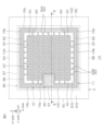
- FIG. 1 is a plan view showing a SiC semiconductor device according to a first embodiment.
- FIG. 2 is a plan view showing the layout of the first main surface.
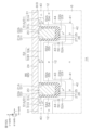
- FIG. 3 is a sectional view taken along the line III-III shown in FIG. 2.
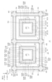
- FIG. 4 is an enlarged plan view showing a main part of the first main surface.
- FIG. 5 is an enlarged plan view showing other main parts of the first main surface.
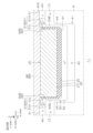
- FIG. 6 is a cross-sectional view taken along line VI-VI shown in FIG. 4.
- FIG. 7 is a sectional view taken along line VII-VII shown in FIG.
- FIG. 8 is an enlarged plan view showing a region including the second trench structure and the third trench structure.
- FIG. 9 is a sectional view taken along line IX-IX shown in FIG. 8.
- FIG. 8 is a sectional view taken along line IX-IX shown in FIG. 8.
- FIG. 10 is a cross-sectional view taken along the line XX shown in FIG. 8.
- FIG. 11 is a sectional view taken along the line XI-XI shown in FIG. 8.
- FIG. 12 is a sectional view taken along the line XII-XII shown in FIG. 8.
- FIG. 13 is a sectional view taken along the line XIII-XIII shown in FIG. 8.
- FIG. 14 is a sectional view taken along the line XIV-XIV shown in FIG. 8.
- FIG. 15 is a sectional view taken along the line XV-XV shown in FIG. 8.
- FIG. 16A is an enlarged cross-sectional view showing a configuration when a region including a second trench structure and a contact region is cut in the m-axis direction.
- FIG. 16B is an enlarged cross-sectional view showing the configuration when a region including the second trench structure and the contact region is cut in the a-axis direction.
- FIG. 17 is a cross-sectional view showing the peripheral edge of the chip.
- FIG. 18 is a plan view showing a SiC semiconductor device according to the second embodiment.
- FIG. 19 is a plan view showing a SiC semiconductor device according to a third embodiment.
- FIG. 20 is a plan view showing a SiC semiconductor device according to the fourth embodiment.
- FIG. 21 is a plan view showing a SiC semiconductor device according to the fifth embodiment.
- FIG. 22 is a plan view showing a SiC semiconductor device according to the sixth embodiment.
- FIG. 23 is a plan view showing a SiC semiconductor device according to a seventh embodiment.
- FIG. 18 is a plan view showing a SiC semiconductor device according to the second embodiment.
- FIG. 19 is a plan view showing a SiC semiconductor device according to a third embodiment.
- FIG. 20 is
- FIG. 24 is a plan view showing a SiC semiconductor device according to the eighth embodiment.
- FIG. 25 is a plan view showing a SiC semiconductor device according to the ninth embodiment.
- FIG. 26 is a sectional view taken along the line XXVI-XXVI shown in FIG. 25.
- FIG. 27 is a sectional view taken along the line XXVII-XXVII shown in FIG. 25.
- FIG. 28A is an enlarged cross-sectional view showing a configuration when a region including a second trench structure and a contact region is cut in the m-axis direction.
- FIG. 28B is an enlarged cross-sectional view showing the configuration when a region including the second trench structure and the contact region is cut in the a-axis direction.
- FIG. 28A is an enlarged cross-sectional view showing a configuration when a region including a second trench structure and a contact region is cut in the m-axis direction.
- FIG. 28B is an enlarged cross-sectional view showing the configuration
- FIG. 29 is a plan view showing a SiC semiconductor device according to the tenth embodiment.
- FIG. 30 is a plan view showing a SiC semiconductor device according to the eleventh embodiment.
- FIG. 31 is a plan view showing a SiC semiconductor device according to the twelfth embodiment.
- FIG. 32 is a plan view showing a SiC semiconductor device according to the thirteenth embodiment.
- FIG. 33 is a plan view showing a SiC semiconductor device according to the fourteenth embodiment.
- FIG. 34 is a plan view showing a SiC semiconductor device according to the fifteenth embodiment.
- FIG. 35 is a cross-sectional view showing a modification of the second trench structure.
- this phrase includes a numerical value (form) that is equal to the numerical value (form) of the comparison target; It also includes a numerical error (form error) in the range of ⁇ 10% based on (form).
- a numerical value that is equal to the numerical value (form) of the comparison target
- a numerical error form error in the range of ⁇ 10% based on (form).
- words such as “first”, “second”, “third”, etc. are used, but these are symbols attached to the name of each structure to clarify the order of explanation; It is not given for the purpose of limiting the name.
- FIG. 1 is a plan view showing a SiC semiconductor device 1A according to the first embodiment.
- FIG. 2 is a plan view showing the layout of the first main surface 3.
- FIG. 3 is a sectional view taken along the line III-III shown in FIG. 2.
- FIG. 4 is an enlarged plan view showing a main part of the first main surface 3.
- FIG. 5 is an enlarged plan view showing other main parts of the first main surface 3.
- FIG. 6 is a cross-sectional view taken along line VI-VI shown in FIG. 4.
- FIG. 7 is a sectional view taken along line VII-VII shown in FIG.
- FIG. 8 is an enlarged plan view showing a region including the second trench structure 20 and the third trench structure 30.
- FIG. 9 is a sectional view taken along line IX-IX shown in FIG. 8.
- FIG. 10 is a cross-sectional view taken along the line XX shown in FIG. 8.
- FIG. 11 is a sectional view taken along the line XI-XI shown in FIG. 8.
- FIG. 12 is a sectional view taken along the line XII-XII shown in FIG. 8.
- FIG. 13 is a sectional view taken along the line XIII-XIII shown in FIG. 8.
- FIG. 14 is a cross-sectional view taken along the line XIV-XIV shown in FIG. 8.
- FIG. 15 is a sectional view taken along the line XV-XV shown in FIG. 8.
- FIG. 16A is an enlarged cross-sectional view showing the configuration when a region including the second trench structure 20 and the contact region 50 is cut in the m-axis direction.
- FIG. 16B is an enlarged cross-sectional view showing the configuration when a region including the second trench structure 20 and the contact region 50 is cut in the a-axis direction.
- FIG. 17 is a cross-sectional view showing the peripheral edge of the chip 2. As shown in FIG.
- SiC semiconductor device 1A is a SiC semiconductor switching device including a SiC-MISFET (Metal Insulator Semiconductor Field Effect Transistor).
- the SiC semiconductor device 1A includes a hexagonal SiC single crystal and includes a chip 2 formed in a hexahedral shape (specifically, a rectangular parallelepiped shape).
- the hexagonal SiC single crystal has multiple types of polytypes including 2H (Hexagonal)-SiC single crystal, 4H-SiC single crystal, 6H-SiC single crystal, and the like.
- the chip 2 includes a 4H-SiC single crystal, but the chip 2 may include other polytypes.
- the chip 2 has a first main surface 3 on one side, a second main surface 4 on the other side, and first to fourth side surfaces 5A to 5D connecting the first main surface 3 and the second main surface 4.
- the first main surface 3 and the second main surface 4 are formed by a c-plane of a SiC single crystal.
- the first principal surface 3 is formed by the silicon plane ((0001) plane) of the SiC single crystal
- the second principal surface 4 is formed by the carbon plane ((000-1) plane) of the SiC single crystal. ing.
- the first main surface 3 and the second main surface 4 are formed into a quadrangular shape in a plan view (hereinafter simply referred to as "plan view") when viewed from the c-axis direction ([0001] direction) of the SiC single crystal. .
- the c-axis direction is the normal direction of the c-plane.
- the c-axis direction is also the thickness direction of the chip 2.
- the first main surface 3 and the second main surface 4 may have an off angle that is inclined at a predetermined angle in a predetermined off direction with respect to the c-plane.
- the off direction is preferably the a-axis direction ([11-20] direction) of the SiC single crystal.
- the off angle may be greater than 0° and less than or equal to 10°.
- the off angle is preferably 5° or less.
- the c-axis is inclined in the off direction by the off angle with respect to the normal to the first main surface 3 (second main surface 4).
- the c-axis extending along the normal to the first main surface 3 (second main surface 4) is illustrated.
- the second main surface 4 may be a ground surface having grinding marks, or may be a smooth surface having no grinding marks.
- the first side surface 5A and the second side surface 5B extend in the a-axis direction of the SiC single crystal and face the m-axis direction ([1-100] direction) of the SiC single crystal. That is, the first side surface 5A and the second side surface 5B are formed by the m-plane ((1-100) plane) of SiC single crystal.
- the third side surface 5C and the fourth side surface 5D extend in the m-axis direction of the SiC single crystal and are opposed to the a-axis direction of the SiC single crystal.
- the third side surface 5C and the fourth side surface 5D are formed by the a-plane ((11-20) plane) of the SiC single crystal.
- the first to fourth side surfaces 5A to 5D may be made of ground surfaces having grinding marks, or may be made of smooth surfaces having no grinding marks.
- the c-axis direction may be referred to as the "thickness direction”
- the a-axis direction may be referred to as the "first direction”
- the m-axis direction may be referred to as the "second direction.”
- the chip 2 may have a thickness of 5 ⁇ m or more and 350 ⁇ m or less.
- the thickness of the chip 2 is in any one of the following ranges: 5 ⁇ m to 50 ⁇ m, 50 ⁇ m to 100 ⁇ m, 100 ⁇ m to 150 ⁇ m, 150 ⁇ m to 200 ⁇ m, 200 ⁇ m to 250 ⁇ m, 250 ⁇ m to 300 ⁇ m, and 300 ⁇ m to 350 ⁇ m. It may be set to the value to which it belongs.
- the thickness of the chip 2 is preferably 150 ⁇ m or less.
- the first to fourth side surfaces 5A to 5D may have a length of 0.5 mm or more and 20 mm or less in plan view.
- the lengths of the first to fourth side surfaces 5A to 5D are set to values belonging to any one of the following ranges: 0.5 mm to 5 mm, 5 mm to 10 mm, 10 mm to 15 mm, and 15 mm to 20 mm. It's okay.
- the lengths of the first to fourth side surfaces 5A to 5D are preferably 5 mm or more.
- the SiC semiconductor device 1A includes an n-type first semiconductor region 6 formed in a region (surface layer portion) on the first main surface 3 side within the chip 2.
- the first semiconductor region 6 may have an n-type impurity concentration (maximum value) of 1.0 ⁇ 10 15 cm ⁇ 3 or more and 1.0 ⁇ 10 17 cm ⁇ 3 or less.
- the first semiconductor region 6 is formed in a layered shape extending along the first main surface 3, and is exposed from the first main surface 3 and the first to fourth side surfaces 5A to 5D.
- the first semiconductor region 6 is made of a SiC epitaxial layer.
- the first semiconductor region 6 may have a thickness of 1 ⁇ m or more and 50 ⁇ m or less.
- the thickness of the first semiconductor region 6 is preferably 5 ⁇ m or more and 30 ⁇ m or less. It is particularly preferable that the thickness of the first semiconductor region 6 is 25 ⁇ m or less.
- the SiC semiconductor device 1A includes an n-type second semiconductor region 7 formed in a region (surface layer portion) on the second main surface 4 side within the chip 2.
- the second semiconductor region 7 is formed in a layered shape extending along the second main surface 4, and is exposed from the second main surface 4 and the first to fourth side surfaces 5A to 5D.
- the second semiconductor region 7 has a higher n-type impurity concentration than the first semiconductor region 6 and is electrically connected to the first semiconductor region 6.
- the second semiconductor region 7 may have an n-type impurity concentration (maximum value) of 1.0 ⁇ 10 18 cm ⁇ 3 or more and 1.0 ⁇ 10 21 cm ⁇ 3 or less.
- the second semiconductor region 7 is made of a SiC substrate. That is, the chip 2 has a stacked structure including a SiC substrate and a SiC epitaxial layer.
- the second semiconductor region 7 may have a thickness of 1 ⁇ m or more and 350 ⁇ m or less.
- the thickness of the second semiconductor region 7 is preferably 5 ⁇ m or more and 50 ⁇ m or less. It is particularly preferable that the thickness of the second semiconductor region 7 is 5 ⁇ m or more and 20 ⁇ m or less.
- the thickness of the second semiconductor region 7 is preferably 10 ⁇ m or more.
- the thickness of the second semiconductor region 7 may exceed the thickness of the first semiconductor region 6.
- the thickness of the second semiconductor region 7 may be less than the thickness of the first semiconductor region 6.
- the SiC semiconductor device 1A includes an active surface 8 formed on the first main surface 3, an outer surface 9, and first to fourth connecting surfaces 10A to 10D.
- the active surface 8, the outer surface 9, and the first to fourth connection surfaces 10A to 10D define an active plateau 11 on the first main surface 3.
- the active surface 8 may be referred to as a "first surface”
- the outer surface 9 may be referred to as a "second surface”
- the first to fourth connection surfaces 10A to 10D may be referred to as "connection surfaces”.
- the active surface 8, the outer surface 9, and the first to fourth connection surfaces 10A to 10D (ie, the active plateau 11) may be considered as constituent elements of the chip 2 (first main surface 3).
- the active surface 8 is formed at a distance inward from the periphery of the first main surface 3 (first to fourth side surfaces 5A to 5D).
- the active surface 8 has a flat surface formed by a c-plane (Si-plane).
- the active surface 8 is formed into a rectangular shape having four sides parallel to the first to fourth side surfaces 5A to 5D in plan view.
- the outer surface 9 is located outside the active surface 8 and is recessed from the active surface 8 in the thickness direction of the chip 2 (toward the second main surface 4 side). Specifically, the outer surface 9 is recessed to a depth less than the thickness of the first semiconductor region 6 so as to expose the first semiconductor region 6.
- the outer surface 9 extends in a band shape along the active surface 8 in a plan view, and is formed into an annular shape (specifically, a square annular shape) surrounding the active surface 8.
- the outer surface 9 has a flat surface formed by a c-plane (Si-plane), and is formed substantially parallel to the active surface 8 .
- the outer surface 9 is continuous with the first to fourth side surfaces 5A to 5D.
- the first to fourth connection surfaces 10A to 10D extend in the c-axis direction and connect the active surface 8 and the outer surface 9.
- the first connection surface 10A is located on the first side surface 5A side
- the second connection surface 10B is located on the second side surface 5B side
- the third connection surface 10C is located on the third side surface 5C side
- the fourth connection surface 10D is located on the third side surface 5C side. is located on the fourth side surface 5D side.
- the first connection surface 10A and the second connection surface 10B extend in the a-axis direction and face each other in the m-axis direction in plan view. That is, the first side surface 5A and the second side surface 5B are formed by the m-plane.
- the third connection surface 10C and the fourth connection surface 10D extend in the m-axis direction and face each other in the a-axis direction in plan view. That is, the third side surface 5C and the fourth side surface 5D are formed by the a-plane.
- the first to fourth connection surfaces 10A to 10D may extend substantially perpendicularly between the active surface 8 and the outer surface 9 so that a quadrangular prism-shaped active plateau 11 is defined.
- the first to fourth connection surfaces 10A to 10D may be inclined downward from the active surface 8 toward the outer surface 9 so that a square pyramid-shaped active plateau 11 is defined.
- the SiC semiconductor device 1A includes an active plateau 11 that is partitioned into a projecting shape in the first semiconductor region 6 on the first main surface 3.
- the active plateau 11 is formed only in the first semiconductor region 6 and not in the second semiconductor region 7.
- SiC semiconductor device 1A includes a p-type body region 12 formed in the surface layer of active surface 8.
- Body region 12 may have a p-type impurity concentration (maximum value) of 1.0 ⁇ 10 16 cm ⁇ 3 or more and 1.0 ⁇ 10 19 cm ⁇ 3 or less.
- the body region 12 is formed in the surface layer of the first semiconductor region 6 at a distance from the bottom of the first semiconductor region 6 toward the active surface 8 side, and is connected to the second semiconductor region 7 with a part of the first semiconductor region 6 in between. is facing.
- the body region 12 is formed in a layer extending along the active surface 8 .
- the body region 12 may be exposed from the first to fourth connection surfaces 10A to 10D.
- the SiC semiconductor device 1A includes a first trench structure 15 formed in the active surface 8.
- a gate potential is applied to the first trench structure 15 .
- the first trench structure 15 may be referred to as a "trench gate wiring structure".
- the first trench structure 15 penetrates the body region 12 and reaches the first semiconductor region 6 .
- the first trench structure 15 is formed at a distance from the bottom of the first semiconductor region 6 toward the active surface 8 side, and faces the second semiconductor region 7 with a part of the first semiconductor region 6 interposed therebetween.
- the first trench structure 15 has a depth approximately equal to the depth of the outer surface 9.
- the first trench structure 15 is formed at the periphery of the active surface 8 at a distance from the periphery (first to fourth connection surfaces 10A to 10D) of the active surface 8, and surrounds the inner part of the active surface 8. It extends in a band shape.
- the first trench structure 15 is formed in an annular shape (specifically, a square annular shape) extending along the first to fourth connection surfaces 10A to 10D.
- the first trench structure 15 includes a pad portion 15a and a line portion 15b.
- the pad portion 15a is arranged at a peripheral portion of the active surface 8 at a distance from the center portion of the third connection surface 10C, and is formed in a rectangular shape in a plan view.
- the line portion 15b is drawn out from the pad portion 15a in a band shape and extends along the periphery of the active surface 8 so as to surround the inner portion of the active surface 8.
- the line portion 15b is formed narrower than the pad portion 15a.
- the first trench structure 15 includes a first trench 16, a first insulating film 17, and a first buried electrode 18.
- the first trench 16 may be called a "wiring trench”
- the first insulating film 17 may be called a “wiring insulating film”
- the first buried electrode 18 may be called a “wiring buried electrode.”
- the first trench 16 is formed in the active surface 8 and defines the walls of the first trench structure 15 .
- the first insulating film 17 covers the wall surface of the first trench 16 in the form of a film.
- the first insulating film 17 may include at least one of a silicon oxide film, a silicon nitride film, and a silicon oxynitride film.
- the first insulating film 17 has a single layer structure made of a silicon oxide film. It is particularly preferable that the first insulating film 17 includes a silicon oxide film made of an oxide of the chip 2 .
- the first buried electrode 18 is buried in the first trench 16 with the first insulating film 17 in between.
- the first buried electrode 18 may protrude above the first main surface 3.
- the first buried electrode 18 may have a portion drawn out from the first trench 16 onto the first main surface 3 .
- the first buried electrode 18 may include conductive polysilicon.
- the SiC semiconductor device 1A includes a plurality of second trench structures 20 formed on the active surface 8.
- a source potential is applied to the plurality of second trench structures 20 .
- the second trench structure 20 may be referred to as a "trench source structure.”
- a plurality of second trench structures 20 are formed inwardly of active surface 8 and spaced apart from first trench structures 15 .
- the plurality of second trench structures 20 penetrate the body region 12 and reach the first semiconductor region 6 .
- the plurality of second trench structures 20 are formed at intervals from the bottom of the first semiconductor region 6 toward the active surface 8 side, and face the second semiconductor region 7 with a part of the first semiconductor region 6 in between. .
- the plurality of second trench structures 20 have a depth approximately equal to the depth of the first trench structure 15.
- the plurality of second trench structures 20 have a depth approximately equal to the depth of the outer surface 9. It is preferable that the second trench structure 20 is formed narrower than the first trench structure 15 .
- the plurality of second trench structures 20 are arranged at intervals in the a-axis direction and the m-axis direction in plan view.
- the plurality of second trench structures 20 may be arranged in a matrix in a plan view.
- the SiC semiconductor device 1A includes a plurality of second trench structures 20 arranged at intervals so as to face each other in the a-axis direction and the m-axis direction.
- the plurality of second trench structures 20 may be arranged in a staggered manner in a plan view.
- the SiC semiconductor device 1A includes a plurality of second trench structures 20 arranged at intervals in a line in the a-axis direction, and a plurality of groups arranged at intervals in the m-axis direction. You can stay there.
- the plurality of second trench structures 20 belonging to one group are arranged in the a-axis direction so as to face a region (for example, an intermediate portion) between the plurality of second trench structures 20 belonging to the other group in the m-axis direction. It is placed off-center.
- the SiC semiconductor device 1A includes a plurality of second trench structures 20 arranged at intervals in a row in the m-axis direction, and a plurality of groups arranged at intervals in the a-axis direction.
- the plurality of second trench structures 20 belonging to one group are arranged in the m-axis direction so as to face a region (for example, an intermediate portion) between the plurality of second trench structures 20 belonging to the other group in the a-axis direction. It is placed off-center.
- the second trench structure 20 is formed into an annular shape (specifically, a square annular shape) extending in the a-axis direction and the m-axis direction in plan view.
- the second trench structure 20 includes an inner wall 21 , an outer wall 22 and a bottom wall 23 .
- the inner wall 21 forms the inner edge of the second trench structure 20 and is formed in a rectangular shape extending in the a-axis direction and the m-axis direction in plan view. Specifically, the inner wall 21 includes a pair of first inner walls 21A and a pair of second inner walls 21B.
- the pair of first inner walls 21A extend in the a-axis direction and face each other in the m-axis direction. That is, the pair of first inner walls 21A are partitioned by the m-plane.
- the pair of second inner walls 21B extend in the m-axis direction so as to be connected to the pair of first inner walls 21A, and face each other in the a-axis direction. That is, the pair of second inner walls 21B are partitioned by the a-plane.
- the inner wall 21 defines a square first mesa portion 24 on the active surface 8 .
- the outer wall 22 forms the outer edge of the second trench structure 20 and surrounds the inner wall 21 in plan view.
- the outer wall 22 is formed into a rectangular shape extending in the a-axis direction and the m-axis direction.
- the outer wall 22 includes a pair of first outer walls 22A and a pair of second outer walls 22B.
- the pair of first outer walls 22A extend in the a-axis direction and face each other in the m-axis direction. In other words, the pair of first outer walls 22A are partitioned by the m-plane.
- the pair of second outer walls 22B extend in the m-axis direction so as to be connected to the pair of first outer walls 22A, and face each other in the a-axis direction. In other words, the pair of second outer walls 22B are partitioned by the a-plane.
- the bottom wall 23 connects the inner wall 21 and the outer wall 22 and is formed into an annular shape (specifically, a square annular shape) extending in the a-axis direction and the m-axis direction in plan view.
- the bottom wall 23 includes a pair of first bottom walls 23A and a pair of second bottom walls 23B.
- the pair of first bottom walls 23A extend in a band shape in the a-axis direction.
- the pair of second bottom walls 23B extend in a band shape in the m-axis direction so as to be connected to the pair of first bottom walls 23A.
- the bottom wall 23 is formed by a c-plane.
- the active surface 8 first main surface 3
- the bottom wall 23 may have an off direction and an off angle.
- the second trench structure 20 includes a second trench 25, a second insulating film 26, and a second buried electrode 27.
- the second trench 25 may be called a "source trench”
- the second insulating film 26 may be called a “source insulating film”
- the second buried electrode 27 may be called a “source buried electrode.”
- the second trench 25 is formed in the active surface 8 and partitions the walls (inner wall 21, outer wall 22, and bottom wall 23) of the second trench structure 20.
- the second insulating film 26 covers the wall surface of the second trench 25 in the form of a film.
- the second insulating film 26 may include at least one of a silicon oxide film, a silicon nitride film, and a silicon oxynitride film.
- the second insulating film 26 has a single layer structure made of a silicon oxide film. It is particularly preferable that the second insulating film 26 includes a silicon oxide film made of an oxide of the chip 2 .
- the second buried electrode 27 is buried in the second trench 25 with the second insulating film 26 interposed therebetween.
- the second buried electrode 27 may include conductive polysilicon.
- the SiC semiconductor device 1A includes a third trench structure 30 formed on the active surface 8 at a distance from the plurality of second trench structures 20. A gate potential is applied to the third trench structure 30.
- the third trench structure 30 may be referred to as a "trench gate structure.” The third trench structure 30 penetrates the body region 12 and reaches the first semiconductor region 6.
- the third trench structure 30 is formed at a distance from the bottom of the first semiconductor region 6 toward the active surface 8 side, and faces the second semiconductor region 7 with a part of the first semiconductor region 6 in between. It is preferable that the third trench structure 30 has a depth substantially equal to the depth of the first trench structure 15 (second trench structure 20). Preferably, the third trench structure 30 has a depth approximately equal to the depth of the outer surface 9. It is preferable that the third trench structure 30 is formed narrower than the first trench structure 15. Preferably, the width of the third trench structure 30 is approximately equal to the width of the second trench structure 20.
- the third trench structure 30 is formed in a lattice shape extending in the a-axis direction and the m-axis direction in a region between the plurality of second trench structures 20 so as to surround the plurality of second trench structures 20 in a plan view.
- the third trench structure 30 is formed in a ring shape (specifically, a square ring shape) surrounding each second trench structure 20 in plan view.
- the third trench structure 30 defines a plurality of second mesa portions 31 extending in an annular shape (specifically, a square annular shape) between the third trench structure 30 and the outer wall 22 of the plurality of second trench structures 20 .
- the third trench structure 30 is electrically and mechanically connected to the first trench structure 15 at the periphery of the active surface 8 .
- the third trench structure 30 includes a plurality of third trench structures 30A extending in the a-axis direction and a plurality of third trench structures 30B extending in the m-axis direction.
- the plurality of third trench structures 30A are formed at intervals in the m-axis direction from the plurality of first outer walls 22A so as to face the plurality of first outer walls 22A in the m-axis direction, and are spaced from the plurality of first outer walls 22A in the m-axis direction.
- the area between 22A and 22A extends in a belt shape in the a-axis direction.
- the plurality of third trench structures 30A are electrically and mechanically connected to the first trench structure 15 at the periphery of the active surface 8.
- Each third trench structure 30A has a pair of first gate side walls 32 extending in the a-axis direction and a first gate bottom wall 33 extending in the a-axis direction.
- the pair of first gate side walls 32 are formed by the m-plane, and the first gate bottom wall 33 is formed by the c-plane.
- the active surface 8 first main surface 3
- the first gate bottom wall 33 Like the main surface 3), it may have an off direction and an off angle.
- the plurality of third trench structures 30B are formed at intervals in the a-axis direction from the plurality of second outer walls 22B so as to face the plurality of second outer walls 22B in the a-axis direction, and are spaced from the plurality of second outer walls 22B in the a-axis direction.
- the region between 22B and 22B extends in a belt shape in the m-axis direction.
- the plurality of third trench structures 30B intersect (specifically, perpendicularly intersect with) the plurality of third trench structures 30A in the inner part of the active surface 8, and form the plurality of trench intersections 34 together with the plurality of third trench structures 30A. is forming.
- the plurality of trench intersections 34 each form a crossroad in plan view.
- the plurality of second trench structures 20 are arranged in a staggered manner in plan view, the plurality of trench intersections 34 each form a T-junction in plan view.
- the plurality of third trench structures 30B are electrically and mechanically connected to the first trench structure 15 at the periphery of the active surface 8.
- Each third trench structure 30B has a pair of second gate side walls 35 extending in the m-axis direction and a second gate bottom wall 36 extending in the m-axis direction.
- the pair of second gate side walls 35 are formed by the a-plane
- the second gate bottom wall 36 is formed by the c-plane.
- the active surface 8 first main surface 3
- the second gate bottom wall 36 Like the main surface 3), it may have an off direction and an off angle.
- the trench intersection 34 is formed by the intersection of the first gate bottom wall 33 and the second gate bottom wall 36 .
- the third trench structure 30 includes a third trench 37, a third insulating film 38, and a third buried electrode 39.
- the third trench 37 may be called a "gate trench”
- the third insulating film 38 may be called a "gate insulating film”
- the third buried electrode 39 may be called a "gate buried electrode.”
- the third trench 37 is formed in the active surface 8 and defines the walls of the third trench structure 30.
- the third trench 37 communicates with the first trench 16 at the peripheral edge of the active surface 8 .
- the third insulating film 38 covers the wall surface of the third trench 37 in the form of a film.
- the third insulating film 38 is connected to the first insulating film 17 at a communication portion between the first trench 16 and the third trench 37 .
- the third insulating film 38 may include at least one of a silicon oxide film, a silicon nitride film, and a silicon oxynitride film.
- the third insulating film 38 has a single layer structure made of a silicon oxide film. It is particularly preferable that the third insulating film 38 includes a silicon oxide film made of the oxide of the chip 2.
- the third buried electrode 39 is buried in the third trench 37 with the third insulating film 38 in between.
- the third buried electrode 39 is electrically and mechanically connected to the first buried electrode 18 at a communication portion between the first trench 16 and the third trench 37 .
- Third buried electrode 39 may include conductive polysilicon.
- SiC semiconductor device 1A includes a plurality of n-type source regions 40 formed in a region along third trench structure 30 in the surface layer portion of body region 12. Specifically, the plurality of source regions 40 are formed in the surface layer portion of the body region 12 in the plurality of second mesa portions 31 . Each source region 40 has a higher n-type impurity concentration than the first semiconductor region 6. The n-type impurity concentration (maximum value) of the source region 40 may be 1.0 ⁇ 10 18 cm ⁇ 3 or more and 1.0 ⁇ 10 21 cm ⁇ 3 or less. The plurality of source regions 40 are formed at intervals from the bottom of the body region 12 toward the active surface 8 , and are formed in a layered shape extending along the active surface 8 .
- each source region 40 is formed in an annular shape (specifically, a rectangular annular shape) extending along the second mesa portion 31 so as to surround each second trench structure 20 in a plan view. and connected to the third trench structure 30.
- Each source region 40 is exposed from the first outer wall 22A and the second outer wall 22B of the second trench structure 20, and is exposed from the first gate side wall 32 and the second gate side wall 35 of the third trench structure 30.
- Each source region 40 forms a channel in the body region 12 together with the first semiconductor region 6 .
- SiC semiconductor device 1A includes a plurality of p-type well regions 41 formed in regions along each second trench structure 20 within chip 2.
- the plurality of well regions 41 have a higher p-type impurity concentration than the body region 12.
- the plurality of well regions 41 may have a lower p-type impurity concentration than the body region 12.
- the p-type impurity concentration (maximum value) of the well region 41 may be 1.0 ⁇ 10 16 cm ⁇ 3 or more and 1.0 ⁇ 10 19 cm ⁇ 3 or less.
- the well region 41 includes a well bottom wall 42, a first well sidewall 43, and a second well sidewall 44.
- the well bottom wall portion 42 is referred to as a “first well portion”
- the first well side wall portion 43 is referred to as a “second well portion”
- the second well side wall portion 44 is referred to as a “third well portion.” Good too.
- the well bottom wall portion 42 is formed in a region along the bottom wall 23 of the second trench structure 20. Specifically, the well bottom wall portion 42 is formed in a region along the pair of first bottom walls 23A and the pair of second bottom walls 23B.
- the well bottom wall portion 42 is formed in an annular shape (specifically, a square annular shape) extending along the bottom wall 23 of the second trench structure 20 in plan view, and covers the entire area of the bottom wall 23 of the second trench structure 20. ing.
- the well bottom wall portion 42 is formed at a distance from the bottom of the first semiconductor region 6 toward the active surface 8 side, and faces the second semiconductor region 7 with a part of the first semiconductor region 6 interposed therebetween.
- the first well side wall portion 43 is drawn out from the well bottom wall portion 42 toward the inner wall 21 side of the second trench structure 20 and is formed in a region along the inner wall 21 . Specifically, the first well side wall portion 43 is formed in a region within the first mesa portion 24 along the pair of first inner walls 21A and the pair of second inner walls 21B.
- the first well side wall portion 43 is formed in an annular shape (specifically, a square annular shape) extending along the inner wall 21 so as to surround the inner part of the body region 12 in a plan view.
- the first well side wall portion 43 is connected to the body region 12 at the surface layer portion of the first mesa portion 24 .
- the thickness of the first well side wall portion 43 with respect to the inner wall 21 is smaller than the thickness of the well bottom wall portion 42 with respect to the bottom wall 23.
- the second well side wall portion 44 is extended from the bottom wall 23 side of the second trench structure 20 to the outer wall 22 side of the second trench structure 20 and is formed in a region along the outer wall 22. Specifically, the second well side wall portion 44 is formed in a region of the second mesa portion 31 along the pair of first outer walls 22A and the pair of second outer walls 22B.
- the second well sidewall portion 44 is formed in an annular shape (specifically, a square annular shape) surrounding the second trench structure 20 at a distance from the third trench structure 30 in the second mesa portion 31 .
- the second well sidewall portion 44 is connected to the body region 12 at the surface layer portion of the second mesa portion 31 .
- the thickness of the second well side wall 44 based on the outer wall 22 is smaller than the thickness of the well bottom wall 42 based on the bottom wall 23.
- SiC semiconductor device 1A includes a plurality of p-type contact regions 50 formed in regions along each second trench structure 20 within chip 2. Specifically, the plurality of contact regions 50 are each formed in a region along the corresponding second trench structure 20 within the corresponding well region 41 .
- the plurality of contact regions 50 have a higher p-type impurity concentration than the body region 12.
- the plurality of contact regions 50 have a higher p-type impurity concentration than the well region 41.
- the p-type impurity concentration (maximum value) of the contact region 50 may be 1.0 ⁇ 10 17 cm ⁇ 3 or more and 1.0 ⁇ 10 21 cm ⁇ 3 or less.
- Contact region 50 preferably contains aluminum (Al) as a p-type impurity.
- the contact region 50 includes at least one (in this embodiment, a plurality of) first regions 51 formed in the surface layer portion of the active surface 8 in the second mesa portion 31 .
- the plurality of first regions 51 are formed in the surface layer portion of the body region 12 in the second mesa portion 31 .
- the plurality of first regions 51 are respectively formed in regions along the outer wall 22 of the second trench structure 20 .
- the plurality of first regions 51 are formed at intervals along the circumferential direction of the outer wall 22.
- the plurality of first regions 51 are formed in a pair of first regions 51A formed in a region along a pair of first outer walls 22A, and in a region along a pair of second outer walls 22B. It includes a pair of first regions 51B. It is preferable that the pair of first regions 51A be narrower than the first outer wall 22A in the a-axis direction. In this embodiment, the pair of first regions 51A are narrower than the first inner wall 21A in the a-axis direction.
- the pair of first regions 51A are formed along the pair of first outer walls 22A with an interval in the a-axis direction from the pair of second outer walls 22B. It is preferable that the pair of first regions 51A face each other in the m-axis direction. It is preferable that the pair of first regions 51A be formed in a region along the center of the pair of first outer walls 22A. Of course, the pair of first regions 51A may be shifted from each other in the a-axis direction so as not to face each other in the m-axis direction.
- each first region 51A in the a-axis direction is preferably 1/2 or less of the width of the first outer wall 22A in the a-axis direction. It is particularly preferable that the width of each first region 51A in the a-axis direction is 1/4 or less of the width of the first outer wall 22A in the a-axis direction. The width of each first region 51A in the a-axis direction may be 1/10 or more of the width of the first outer wall 22A in the a-axis direction.
- the pair of first regions 51B be formed narrower than the second outer wall 22B in the m-axis direction.
- the pair of first regions 51B are formed narrower than the second inner wall 21B in the m-axis direction.
- the pair of first regions 51B are formed in regions along the pair of second outer walls 22B at intervals in the m-axis direction from the pair of first outer walls 22A.
- the pair of first regions 51B face each other in the a-axis direction. It is preferable that the pair of first regions 51B be formed in a region along the center of the second outer wall 22B. Of course, the pair of first regions 51B may be shifted from each other in the m-axis direction so as not to face each other in the a-axis direction.
- each first region 51B in the m-axis direction is preferably 1/2 or less of the width of the second outer wall 22B in the m-axis direction. It is particularly preferable that the width of each first region 51B in the m-axis direction is 1/4 or less of the width of the second outer wall 22B in the m-axis direction. The width of each first region 51B in the m-axis direction may be 1/10 or more of the width of the second outer wall 22B in the m-axis direction.
- first region 51 is formed at a distance from the bottom of body region 12 toward active surface 8, and faces first semiconductor region 6 with a part of body region 12 in between. are doing. That is, the first region 51 has a bottom located within the body region 12.
- the first region 51 is formed at a distance from the third trench structure 30 toward the second trench structure 20 and is connected to the source region 40 .
- the first region 51 has a concentration gradient in which the p-type impurity concentration decreases from the active surface 8 side toward the bottom side.
- the first region 51 includes the first high concentration region 51H on the side of the active surface 8 and the first low concentration region 51L on the bottom side, and p It has a concentration gradient in which the type impurity concentration decreases.
- the first high concentration region 51H has the maximum p-type impurity concentration and the p-type impurity concentration is the region between the intermediate values of .
- the first low concentration region 51L is a region between the intermediate value of the p-type impurity concentration and the minimum value of the p-type impurity concentration.
- the maximum and minimum values of the p-type impurity concentration of the first high concentration region 51H are higher than the maximum value of the p-type impurity concentration of the body region 12.
- the maximum value of the p-type impurity concentration of the first high concentration region 51H may be 1.0 ⁇ 10 19 cm ⁇ 3 or more and 1.0 ⁇ 10 21 cm ⁇ 3 or less.
- the first high concentration region 51H extends in a layered manner along the active surface 8 and is connected to the second trench structure 20 and the source region 40.
- the maximum and minimum values of the p-type impurity concentration of the first low concentration region 51L are lower than the minimum value of the first high concentration region 51H and higher than the maximum value of the p-type impurity concentration of the body region 12.
- the minimum value of the p-type impurity concentration of the first low concentration region 51L is preferably 1/1000 or more and 1/2 or less of the maximum value of the p-type impurity concentration of the first high concentration region 51H.
- the minimum value of the p-type impurity concentration of the first low concentration region 51L may be 1.0 ⁇ 10 17 cm ⁇ 3 or more and 1.0 ⁇ 10 20 cm ⁇ 3 or less.
- the first low concentration region 51L extends in a layered manner along the first high concentration region 51H (active surface 8) and is connected to the second trench structure 20 and the source region 40.
- the first low concentration region 51L may have a thickness greater than or equal to the thickness of the first high concentration region 51H, or may have a thickness less than the thickness of the first high concentration region 51H. .
- the boundary between the first high concentration region 51H and the first low concentration region 51L may be located on the active surface 8 side with respect to the intermediate portion in the thickness direction of the first region 51, or It may be located on the bottom side of the area 51.
- the contact region 50 includes at least one (in this form, a plurality of) second regions 52 formed in a region along the bottom wall 23 of the second trench structure 20 in the chip 2 .
- the plurality of second regions 52 are formed within the well region 41 in regions along the bottom wall 23 of the second trench structure 20 at intervals from the bottom of the body region 12 . That is, the plurality of second regions 52 are formed within the well bottom wall portion 42.
- the plurality of second regions 52 are formed at intervals along the circumferential direction of the bottom wall 23.
- the plurality of second regions 52 are a pair of second regions 52A formed in a region along a pair of first bottom walls 23A, and a region along a pair of second bottom walls 23B. It includes a pair of second regions 52B.
- the pair of second regions 52A be narrower than the first outer wall 22A in the a-axis direction.
- the pair of second regions 52A are formed to be narrower than the first inner wall 21A in the a-axis direction.
- the pair of second regions 52A are formed in regions along the pair of first bottom walls 23A at intervals in the a-axis direction from the pair of second bottom walls 23B. It is preferable that the pair of second regions 52A face each other in the m-axis direction.
- the pair of second regions 52A are preferably formed in a region along the center of the pair of first bottom walls 23A.
- the pair of second regions 52A faces the pair of first regions 51A in the m-axis direction.
- the pair of second regions 52A may be shifted from each other in the a-axis direction so as not to face each other in the m-axis direction.
- one second region 52A preferably faces one adjacent first region 51A in the m-axis direction
- the other second region 52B faces the other adjacent first region 51A in the m-axis direction. It is preferable that they face each other.
- each second region 52A in the a-axis direction is preferably 1/2 or less of the width of the first bottom wall 23A in the a-axis direction. It is particularly preferable that the width of each second region 52A in the a-axis direction is 1/4 or less of the width of the first bottom wall 23A in the a-axis direction. The width of each second region 52A in the a-axis direction may be 1/10 or more of the width of the first bottom wall 23A in the a-axis direction. The width of each second region 52A in the a-axis direction is preferably approximately equal to the width of each first region 51A in the a-axis direction.
- the pair of second regions 52B be narrower than the second outer wall 22B in the m-axis direction.
- the pair of second regions 52B are formed narrower than the second inner wall 21B in the m-axis direction.
- the pair of second regions 52B are formed in regions along the pair of second bottom walls 23B at intervals in the m-axis direction from the pair of first bottom walls 23A. It is preferable that the pair of second regions 52B face each other in the a-axis direction.
- the pair of second regions 52B are preferably formed in a region along the center of the pair of second bottom walls 23B.
- the pair of second regions 52B face the pair of first regions 51B in the a-axis direction.
- the pair of second regions 52B may be shifted from each other in the m-axis direction so as not to face each other in the a-axis direction.
- one second region 52B preferably faces one adjacent first region 51B in the a-axis direction
- the other second region 52B faces the other adjacent first region 51B in the a-axis direction. It is preferable that they face each other.
- each second region 52B in the m-axis direction is preferably 1/2 or less of the width of the second bottom wall 23B in the m-axis direction. It is particularly preferable that the width of each second region 52B in the m-axis direction is 1/4 or less of the width of the second bottom wall 23B in the m-axis direction. The width of each second region 52B in the m-axis direction may be 1/10 or more of the width of the second bottom wall 23B in the m-axis direction. The width of each second region 52B in the m-axis direction is preferably approximately equal to the width of each first region 51B in the m-axis direction.
- second region 52 is formed at a distance from the bottom of well region 41 toward bottom wall 23 of second trench structure 20, with a part of well region 41 sandwiched therebetween. 1 semiconductor region 6 . That is, the second region 52 has a bottom located within the well region 41. The second region 52 extends in a layered manner along the bottom wall 23 and is connected to the bottom wall 23 of the second trench structure 20 .
- the second region 52 unlike the first region 51, does not include the first high concentration region 51H and the first low concentration region 51L.
- the maximum value of the p-type impurity concentration in the second region 52 is lower than the maximum value of the p-type impurity concentration in the first region 51.
- the second region 52 may have a substantially constant p-type impurity concentration in the thickness direction.
- the second region 52 may have a concentration gradient in which the p-type impurity concentration decreases from the bottom wall 23 toward the well region 41. In this case, the rate of decrease in the p-type impurity concentration in the second region 52 is less than the rate of decrease in the p-type impurity concentration in the first region 51.
- the maximum p-type impurity concentration of the second region 52 is lower than the maximum p-type impurity concentration of the first high concentration region 51H and higher than the maximum p-type impurity concentration of the well region 41.
- the maximum value of the p-type impurity concentration in the second region 52 is preferably equal to or less than the intermediate value of the p-type impurity concentration in the first region 51.
- the minimum value of the p-type impurity concentration in the second region 52 is preferably approximately equal to the minimum value of the p-type impurity concentration in the first low concentration region 51L.
- the maximum value of the p-type impurity concentration in the second region 52 is preferably 1/1000 or more and 1/2 or less of the maximum value of the p-type impurity concentration in the first high concentration region 51H.
- the maximum value of the p-type impurity concentration in the second region 52 may be 1.0 ⁇ 10 17 cm ⁇ 3 or more and 1.0 ⁇ 10 20 cm ⁇ 3 or less.
- the maximum value of the p-type impurity concentration of the second region 52 is the same as that of the first low-concentration region 51L.
- the p-type impurity concentration may be less than the maximum value.
- the second region 52 has a thickness greater than the thickness of the first high concentration region 51H. Further, the second region 52 has a thickness greater than the thickness of the first low concentration region 51L. The thickness of the second region 52 may be less than or equal to the thickness of the first region 51, or may be greater than the thickness of the first region 51. The thickness of the second region 52 is preferably approximately equal to the thickness of the first region 51.
- the contact region 50 includes at least one (one in this form) third region 53 formed in the surface layer portion of the active surface 8 in the first mesa portion 24 .
- the third region 53 is formed in the surface layer portion of the body region 12 in the first mesa portion 24 .
- the third region 53 is formed over the entire surface layer portion of the body region 12 in the first mesa portion 24 and is connected to the inner wall 21 of the second trench structure 20 .
- the third region 53 is connected to a pair of first inner walls 21A and a pair of second inner walls 21B.
- the third region 53 is formed at a distance from the bottom of the body region 12 toward the active surface 8 side, and faces the first semiconductor region 6 with a part of the body region 12 interposed therebetween. That is, the third region 53 has a bottom located within the body region 12.
- the third region 53 has a concentration gradient in which the p-type impurity concentration decreases from the active surface 8 side toward the bottom side.
- the third region 53 includes a second high concentration region 53H on the active surface 8 side and a second low concentration region 53L on the bottom side, and the third region 53 includes a second high concentration region 53H on the side of the active surface 8 and a second low concentration region 53L on the bottom side. It has a concentration gradient in which the type impurity concentration decreases.
- the second high concentration region 53H has the maximum p-type impurity concentration and the p-type impurity concentration is the region between the intermediate values of .
- the second low concentration region 53L is a region between the intermediate value of the p-type impurity concentration and the minimum value of the p-type impurity concentration.
- the maximum value and minimum value of the second high concentration region 53H are higher than the maximum value of the p-type impurity concentration of the body region 12.
- the maximum value of the p-type impurity concentration of the second high concentration region 53H may be 1.0 ⁇ 10 19 cm ⁇ 3 or more and 1.0 ⁇ 10 21 cm ⁇ 3 or less.
- the p-type impurity concentration of the second high concentration region 53H is approximately equal to the p-type impurity concentration of the first high concentration region 51H of the first region 51.
- the second high concentration region 53H extends in a layered manner along the active surface 8 and is connected to the inner wall 21 (the first inner wall 21A and the second inner wall 21B) of the second trench structure 20.
- the maximum and minimum values of the p-type impurity concentration of the second low concentration region 53L are lower than the minimum value of the second high concentration region 53H and higher than the maximum value of the p-type impurity concentration of the body region 12.
- the minimum value of the p-type impurity concentration of the second low concentration region 53L is preferably 1/1000 or more and 1/2 or less of the maximum value of the p-type impurity concentration of the second high concentration region 53H.
- the minimum value of the p-type impurity concentration of the second low concentration region 53L may be 1.0 ⁇ 10 17 cm ⁇ 3 or more and 1.0 ⁇ 10 20 cm ⁇ 3 or less.
- the p-type impurity concentration of the second low concentration region 53L is approximately equal to the p-type impurity concentration of the first low concentration region 51L of the first region 51.
- the second low concentration region 53L extends in a layered manner along the second high concentration region 53H (active surface 8) and is connected to the inner wall 21 (first inner wall 21A and second inner wall 21B) of the second trench structure 20. has been done.
- the second low concentration region 53L may have a thickness greater than or equal to the thickness of the second high concentration region 53H, or may have a thickness less than the thickness of the second high concentration region 53H. .
- the boundary between the second high concentration region 53H and the second low concentration region 53L may be located on the active surface 8 side with respect to the intermediate portion in the thickness direction of the third region 53, or It may be located on the bottom side of the area 53.
- the second high concentration region 53H thickly. That is, it is preferable that the second low concentration region 53L has a thickness less than the thickness of the second high concentration region 53H.
- the second high concentration region 53H has a thickness approximately equal to the thickness of the first high concentration region 51H
- the first high concentration region 51H has a thickness approximately equal to the thickness of the second high concentration region 53H.
- the relationship in p-type impurity concentration between the second high concentration region 53H and the second region 52 is almost the same as the relationship in the p-type impurity concentration between the first high concentration region 51H and the second region 52. be. Further, the relationship in p-type impurity concentration that holds true between the second low concentration region 53L and the second region 52 is approximately the same as the relationship in p-type impurity concentration that holds true between the first low concentration region 51L and the second region 52. It's the same.
- the contact region 50 includes at least one (in this embodiment, a plurality of) first connection regions 54 formed in a region along the outer wall 22 of the second trench structure 20 in the chip 2 .
- the plurality of first connection regions 54 are arranged along the outer wall 22 of the second trench structure 20 within the well region 41 so as to connect the first region 51 and the second region 52 that are adjacent to each other in the vertical direction. are formed in each area.
- the plurality of second regions 52 are formed within the second well side wall portion 44 .
- the plurality of first connection regions 54 include a pair of first connection regions 54A formed in a region along a pair of first outer walls 22A in the chip 2, and a pair of second connection regions 54A formed in a region along a pair of first outer walls 22A in the chip 2. It includes a pair of first connection regions 54B formed in regions along the outer wall 22B.
- the pair of first connection regions 54A are formed in regions along the corresponding first outer walls 22A so as to connect the first region 51A and the second region 52A that are close to each other in the vertical direction.
- the pair of first connection regions 54A be narrower than the first outer wall 22A in the a-axis direction.
- the pair of first connection regions 54A are formed narrower in width than the first inner wall 21A in the a-axis direction.
- the pair of first connection regions 54A are formed in regions along the pair of first outer walls 22A at intervals in the a-axis direction from the pair of second outer walls 22B.
- the pair of first connection regions 54A are preferably formed in a region along the center of the pair of first outer walls 22A. The formation locations of the pair of first connection regions 54A are adjusted according to the formation locations of the corresponding first region 51A and second region 52A.
- each first connection region 54A in the a-axis direction is preferably 1/2 or less of the width of the first outer wall 22A in the a-axis direction. It is particularly preferable that the width of each first connection region 54A in the a-axis direction is 1/4 or less of the width of the first outer wall 22A in the a-axis direction. The width of each first connection region 54A in the a-axis direction may be 1/10 or more of the width of the first outer wall 22A in the a-axis direction. The width of each first connection region 54A in the a-axis direction is preferably approximately equal to the width of each first region 51A in the a-axis direction and the width of each second region 52A in the a-axis direction.
- the pair of first connection regions 54B are formed in regions along the corresponding second outer walls 22B so as to connect the first region 51B and the second region 52B that are close to each other in the vertical direction. It is preferable that the pair of first connection regions 54B be narrower than the second outer wall 22B in the m-axis direction. In this embodiment, the pair of first connection regions 54B are formed narrower than the second inner wall 21B in the m-axis direction.
- the pair of first connection regions 54B are formed in regions along the pair of second outer walls 22B at intervals in the m-axis direction from the pair of first outer walls 22A.
- the pair of first connection regions 54A are preferably formed in a region along the center of the pair of second outer walls 22B.
- the formation locations of the pair of first connection regions 54B are adjusted according to the formation locations of the corresponding first region 51B and second region 52B.
- each first connection region 54B in the m-axis direction is preferably 1/2 or less of the width of the second outer wall 22B in the m-axis direction. It is particularly preferable that the width of each first connection region 54B in the m-axis direction is 1/4 or less of the width of the second outer wall 22B in the m-axis direction. The width of each first connection region 54B in the m-axis direction may be 1/10 or more of the width of the second outer wall 22B in the m-axis direction. The width of each first connection region 54B in the m-axis direction is preferably approximately equal to the width of each first region 51B in the m-axis direction and the width of each second region 52B in the m-axis direction.
- first connection region 54 is attached to outer wall 22 of second trench structure 20 so as to be drawn out from inside well region 41 (second well side wall portion 44) into body region 12. It is formed in a layered manner extending along the c-axis direction.
- the first connection region 54 is connected to the first region 51 on the surface layer side of the active surface 8 and to the second region 52 on the bottom wall 23 side of the second trench structure 20 .
- the first connection region 54 is connected to the first low concentration region 51L of the first region 51.
- the first connection region 54 faces the first semiconductor region 6 in the horizontal direction with a part of the well region 41 (second well side wall portion 44) interposed therebetween.
- the first connection region 54 unlike the first region 51, does not include the first high concentration region 51H and the first low concentration region 51L.
- the maximum value of the p-type impurity concentration in the first connection region 54 is lower than the maximum value of the p-type impurity concentration in the first region 51.
- the first connection region 54 may have a substantially constant p-type impurity concentration in the horizontal direction.
- the first connection region 54 may have a concentration gradient in which the p-type impurity concentration decreases in the horizontal direction from the outer wall 22 of the second trench structure 20. In this case, the rate of decrease in the p-type impurity concentration in the first connection region 54 is less than the rate of decrease in the p-type impurity concentration in the first region 51.
- the maximum and minimum values of the p-type impurity concentration of the first connection region 54 are lower than the maximum value of the p-type impurity concentration of the first high concentration region 51H, and are lower than the maximum value of the p-type impurity concentration of the well region 41. It's also expensive. It is preferable that the maximum value of the p-type impurity concentration of the first connection region 54 is equal to or lower than the intermediate value of the p-type impurity concentration of the first region 51.
- the minimum value of the p-type impurity concentration of the first connection region 54 is preferably approximately equal to the minimum value of the p-type impurity concentration of the first low concentration region 51L.
- the maximum value of the p-type impurity concentration of the first connection region 54 is preferably 1/1000 or more and 1/2 or less of the maximum value of the p-type impurity concentration of the first high concentration region 51H.
- the maximum value of the p-type impurity concentration of the first connection region 54 may be 1.0 ⁇ 10 17 cm ⁇ 3 or more and 1.0 ⁇ 10 20 cm ⁇ 3 or less.
- the maximum value of the p-type impurity concentration of the first connection region 54 is may be less than the maximum p-type impurity concentration.
- the thickness of the first connection region 54 with respect to the outer wall 22 is smaller than the thickness of the first region 51 with respect to the active surface 8.
- the thickness of the first connection region 54 with respect to the outer wall 22 is smaller than the thickness of the second region 52 with respect to the bottom wall 23 of the second trench structure 20 .
- the thickness of the first connection region 54 may be less than or equal to the thickness of the first high concentration region 51H, or may exceed the thickness of the first high concentration region 51H.
- the thickness of the first connection region 54 may be less than or equal to the thickness of the first low concentration region 51L, or may exceed the thickness of the first low concentration region 51L.
- the relationship in p-type impurity concentration and thickness between the first connection region 54 and the third region 53 is similar to the relationship in p-type impurity concentration and thickness between the first connection region 54 and the first region 51. Therefore, its explanation will be omitted.
- the contact region 50 includes at least one (in this embodiment, a plurality of) second connection regions 55 formed in a region along the inner wall 21 of the second trench structure 20 in the chip 2 .
- the plurality of second connection regions 55 are each formed in a region along the inner wall 21 of the second trench structure 20 in the well region 41 so as to connect the plurality of second regions 52 and third regions 53, respectively. It is formed. That is, the plurality of second regions 52 are formed within the first well side wall portion 43.
- the plurality of second connection regions 55 include a pair of second connection regions 55A formed in regions along the pair of first inner walls 21A within the chip 2, and a pair of second connection regions 55A formed within the chip 2 in regions along the pair of first inner walls 21A. It includes a pair of second connection regions 55B formed in regions along the inner wall 21B.
- the pair of second connection regions 55A are formed in regions along the corresponding first inner walls 21A so as to connect the pair of second regions 52A and third region 53.
- the pair of second connection regions 55A be formed narrower in the a-axis direction than the first inner wall 21A.
- the pair of second connection regions 55A are formed in regions along the pair of first inner walls 21A at intervals in the a-axis direction from the pair of second inner walls 21B.
- the pair of second connection regions 55A are preferably formed in a region along the center of the pair of first inner walls 21A. The formation locations of the pair of second connection regions 55A are adjusted according to the formation locations of the corresponding second regions 52A.
- each second connection region 55A in the a-axis direction is preferably 1/2 or less of the width of the first inner wall 21A in the a-axis direction. It is particularly preferable that the width of each second connection region 55A in the a-axis direction is 1/3 or less of the width of the first inner wall 21A in the a-axis direction. The width of each second connection region 55A in the a-axis direction may be 1/10 or more of the width of the first inner wall 21A in the a-axis direction. The width of each second connection region 55A in the a-axis direction is preferably approximately equal to the width of each second region 52A in the a-axis direction.
- the pair of second connection regions 55B are formed in regions along the corresponding second inner walls 21B so as to connect the pair of second regions 52B and third region 53. It is preferable that the pair of second connection regions 55B be narrower than the second inner wall 21B in the m-axis direction.
- the pair of second connection regions 55B are formed in regions along the pair of second inner walls 21B at intervals in the m-axis direction from the pair of first inner walls 21A.
- the pair of second connection regions 55B are preferably formed in a region along the center of the pair of second inner walls 21B. The formation locations of the pair of second connection regions 55B are adjusted according to the formation locations of the corresponding second regions 52B.
- each second connection region 55B in the m-axis direction is preferably 1/2 or less of the width of the second inner wall 21B in the m-axis direction. It is particularly preferable that the width of each second connection region 55B in the m-axis direction is 1/3 or less of the width of the second inner wall 21B in the m-axis direction. The width of each second connection region 55B in the m-axis direction may be 1/10 or more of the width of the second inner wall 21B in the m-axis direction. The width of each second connection region 55B in the m-axis direction is preferably approximately equal to the width of each second region 52B in the m-axis direction.
- second connection region 55 is attached to inner wall 21 of second trench structure 20 so as to be drawn out from well region 41 (first well side wall portion 43) into body region 12. It is formed in a layered manner extending along the c-axis direction.
- the second connection region 55 is connected to the second region 52 on the bottom wall 23 side of the second trench structure 20 and to the third region 53 on the surface layer side of the active surface 8 .
- the second connection region 55 is connected to the second low concentration region 53L of the third region 53.
- the second connection region 55 faces the first semiconductor region 6 in the horizontal direction with a part of the well region 41 (first well side wall portion 43) interposed therebetween.
- the second connection region 55 does not include the first high concentration region 51H and the first low concentration region 51L.
- the maximum value of the p-type impurity concentration in the second connection region 55 is lower than the maximum value of the p-type impurity concentration in the first region 51.
- the second connection region 55 may have a substantially constant p-type impurity concentration in the horizontal direction.
- the second connection region 55 may have a concentration gradient in which the p-type impurity concentration decreases in the horizontal direction from the inner wall 21 of the second trench structure 20. In this case, the rate of decrease in the p-type impurity concentration in the second connection region 55 is less than the rate of decrease in the p-type impurity concentration in the first region 51.
- the maximum and minimum values of the p-type impurity concentration of the second connection region 55 are lower than the maximum value of the p-type impurity concentration of the first high concentration region 51H and lower than the maximum value of the p-type impurity concentration of the well region 41. It's also expensive.
- the maximum value of the p-type impurity concentration in the second connection region 55 is preferably equal to or less than the intermediate value of the p-type impurity concentration in the first region 51.
- the minimum value of the p-type impurity concentration of the first connection region 54 is preferably approximately equal to the minimum value of the p-type impurity concentration of the first low concentration region 51L.
- the maximum value of the p-type impurity concentration of the second connection region 55 is preferably 1/1000 or more and 1/2 or less of the maximum value of the p-type impurity concentration of the first high concentration region 51H.
- the maximum value of the p-type impurity concentration of the second connection region 55 may be 1.0 ⁇ 10 17 cm ⁇ 3 or more and 1.0 ⁇ 10 20 cm ⁇ 3 or less.
- the maximum value of the p-type impurity concentration of the second connection region 55 is may be less than the maximum p-type impurity concentration.
- the thickness of the second connection region 55 with respect to the inner wall 21 is smaller than the thickness of the first region 51 with respect to the active surface 8.
- the thickness of the second connection region 55 with respect to the inner wall 21 is smaller than the thickness of the second region 52 with respect to the bottom wall 23 of the second trench structure 20 .
- the thickness of the second connection region 55 may be less than or equal to the thickness of the first high concentration region 51H, or may exceed the thickness of the first high concentration region 51H.
- the thickness of the second connection region 55 may be less than or equal to the thickness of the first low concentration region 51L, or may exceed the thickness of the first low concentration region 51L.
- the relationship in p-type impurity concentration and thickness between the second connection region 55 and the third region 53 is similar to the relationship in p-type impurity concentration and thickness between the second connection region 55 and the first region 51. Therefore, its explanation will be omitted.
- SiC semiconductor device 1A includes a plurality of p-type gate well regions 65 formed in regions along a plurality of trench intersections 34 within chip 2.
- the plurality of gate well regions 65 have a lower p-type impurity concentration than the contact region 50.
- the plurality of gate well regions 65 have a higher p-type impurity concentration than the body region 12.
- the plurality of gate well regions 65 may have a lower p-type impurity concentration than the body region 12.
- the plurality of gate well regions 65 have approximately the same p-type impurity concentration as the well region 41.
- the p-type impurity concentration (maximum value) of the gate well region 65 may be 1.0 ⁇ 10 16 cm ⁇ 3 or more and 1.0 ⁇ 10 19 cm ⁇ 3 or less.
- the plurality of gate well regions 65 are formed in regions along the plurality of trench intersections 34 at intervals in the a-axis direction and the m-axis direction, and are formed on the bottom wall of the third trench structure 30 (the first gate bottom wall 33 and the first gate bottom wall 33). A region of the two-gate bottom wall 36) outside the plurality of trench intersections 34 is exposed.
- Each gate well region 65 covers the first gate side wall 32 of the third trench structure 30A and the second gate side wall 35 of the third trench structure 30B at the corner of each second mesa portion 31, and It is connected to the body region 12 at the surface layer portion.
- the plurality of gate well regions 65 are formed at intervals from the bottom of the first semiconductor region 6 toward the active surface 8 side, and face the second semiconductor region 7 with a part of the first semiconductor region 6 in between.
- the bottoms of the plurality of gate well regions 65 are preferably formed at approximately the same depth as the bottoms of the well regions 41.
- SiC semiconductor device 1A includes a wiring well region 66 formed in a region along the wall surface of first trench structure 15 within chip 2.
- Wiring well region 66 has a lower p-type impurity concentration than contact region 50. In this form, wiring well region 66 has a higher p-type impurity concentration than body region 12.
- the wiring well region 66 may have a lower p-type impurity concentration than the body region 12.
- wiring well region 66 has approximately the same p-type impurity concentration as well region 41 .
- the p-type impurity concentration (maximum value) of the wiring well region 66 may be 1.0 ⁇ 10 16 cm ⁇ 3 or more and 1.0 ⁇ 10 19 cm ⁇ 3 or less.
- the wiring well region 66 is formed in the pad portion 15 a and the line portion 15 b of the first trench structure 15 in a region along the inner wall, outer wall, and bottom wall of the first trench structure 15 , and is formed in the body region 12 in the surface layer portion of the active surface 8 . It is connected to the.
- the wiring well region 66 is formed at a distance from the bottom of the first semiconductor region 6 toward the active surface 8 side, and faces the second semiconductor region 7 with a part of the first semiconductor region 6 interposed therebetween.
- the bottom of the wiring well region 66 is preferably formed at a depth approximately equal to the bottom of the well region 41.
- SiC semiconductor device 1A includes a p-type outer well region 67 formed in the surface layer portion of outer surface 9.
- Outer well region 67 has a lower p-type impurity concentration than contact region 50.
- outer well region 67 has a higher p-type impurity concentration than body region 12.
- outer well region 67 may have a lower p-type impurity concentration than body region 12.
- outer well region 67 has approximately the same p-type impurity concentration as well region 41 .
- the p-type impurity concentration (maximum value) of the outer well region 67 may be 1.0 ⁇ 10 16 cm ⁇ 3 or more and 1.0 ⁇ 10 19 cm ⁇ 3 or less.
- the outer well region 67 is formed at a distance from the periphery of the outer surface 9 (first to fourth side surfaces 5A to 5D) toward the active surface 8 in a plan view, and extends in a band shape along the active surface 8.
- the outer well region 67 is formed in an annular shape (specifically, a square annular shape) surrounding the active surface 8 in plan view.
- the outer well region 67 extends from the surface layer of the outer surface 9 toward the surface layer portions of the first to fourth connection surfaces 10A to 10D, and covers the first to fourth connection surfaces 10A to 10D.
- Outer well region 67 is electrically connected to body region 12 at the surface layer of active surface 8 .
- the outer well region 67 is formed at a distance from the bottom of the first semiconductor region 6 toward the outer surface 9 side, and faces the second semiconductor region 7 with a part of the first semiconductor region 6 in between.
- the outer well region 67 is located closer to the bottom of the first semiconductor region 6 than the bottom walls 23 of the plurality of second trench structures 20 are.
- the bottom of the outer well region 67 is located closer to the bottom of the first semiconductor region 6 than the bottom of the contact region 50 (the bottom of the second region 52).
- the bottom of the outer well region 67 is preferably formed at a depth approximately equal to the bottom of the well region 41.
- the SiC semiconductor device 1A includes a p-type outer contact region 68 formed in the surface layer portion of the outer well region 67.
- the outer contact region 68 is located in the outer well at a distance from the periphery of the active surface 8 (first to fourth connection surfaces 10A to 10D) and the periphery of the outer surface 9 (first to fourth side surfaces 5A to 5D) in plan view. It is formed in the surface layer part of the region 67 and is formed in a band shape extending along the active surface 8 .
- the outer contact region 68 is formed in an annular shape (specifically, a square annular shape) surrounding the active surface 8 in plan view.
- the outer contact region 68 is formed at a distance from the bottom of the outer well region 67 toward the outer surface 9 side, and faces the first semiconductor region 6 with a part of the outer well region 67 in between.
- the outer contact region 68 is located closer to the bottom of the first semiconductor region 6 than the bottom walls 23 of the plurality of second trench structures 20 are.
- the bottom of the outer contact region 68 is preferably formed at a depth approximately equal to the bottom of the contact region 50 (the bottom of the second region 52).
- Outer contact region 68 has a higher p-type impurity concentration than body region 12. Outer contact region 68 has a higher p-type impurity concentration than outer well region 67.
- the p-type impurity concentration (maximum value) of the outer contact region 68 may be 1.0 ⁇ 10 17 cm ⁇ 3 or more and 1.0 ⁇ 10 21 cm ⁇ 3 or less.
- outer contact region 68 has approximately the same p-type impurity concentration as first region 51 of contact region 50 .
- the outer contact region 68 preferably contains aluminum (Al) as a p-type impurity.
- the outer contact region 68 has a concentration gradient in which the p-type impurity concentration decreases from the outer surface 9 side toward the bottom side.
- the outer contact region 68 includes a third high concentration region 68H on the outer surface 9 side and a third low concentration region 68L on the bottom side, and p It has a concentration gradient in which the type impurity concentration decreases.
- the third high concentration region 68H has the maximum p-type impurity concentration and the p-type impurity concentration. is the region between the intermediate values of .
- the third low concentration region 68L is a region between the intermediate value of the p-type impurity concentration and the minimum value of the p-type impurity concentration.
- the maximum and minimum values of the p-type impurity concentration of the third high concentration region 68H are higher than the p-type impurity concentration of the outer well region 67.
- the maximum value of the p-type impurity concentration of the third high concentration region 68H may be 1.0 ⁇ 10 19 cm ⁇ 3 or more and 1.0 ⁇ 10 21 cm ⁇ 3 or less. It is preferable that the p-type impurity concentration of the third high concentration region 68H is approximately equal to the p-type impurity concentration of the first high concentration region 51H.
- the third high-concentration region 68H extends in a band shape (annular in this embodiment) along the outer surface 9 in a plan view, and is exposed from the outer surface 9.
- the maximum and minimum values of the p-type impurity concentration of the third low concentration region 68L are lower than the minimum value of the first high concentration region 51H and higher than the maximum value of the p-type impurity concentration of the outer well region 67.
- the minimum value of the p-type impurity concentration of the third low concentration region 68L is preferably 1/1000 or more and 1/2 or less of the maximum value of the p-type impurity concentration of the third high concentration region 68H.
- the minimum value of the p-type impurity concentration of the third low concentration region 68L may be 1.0 ⁇ 10 17 cm ⁇ 3 or more and 1.0 ⁇ 10 20 cm ⁇ 3 or less.
- the p-type impurity concentration of the third low concentration region 68L is preferably approximately equal to the p-type impurity concentration of the first low concentration region 51L.
- the third low concentration region 68L extends in a band shape (in this embodiment, annular shape) along the outer surface 9 in plan view.
- the third low concentration region 68L may have a thickness greater than or equal to the thickness of the third high concentration region 68H, or may have a thickness less than the thickness of the third high concentration region 68H. .
- the boundary between the third high concentration region 68H and the third low concentration region 68L may be located on the outer surface 9 side with respect to the intermediate portion in the thickness direction of the outer well region 67, or It may be located on the bottom side of the area 67.
- the SiC semiconductor device 1A includes at least one (preferably 2 or more and 20 or less) p-type field regions formed in the surface layer of the outer surface 9 in a region between the periphery of the outer surface 9 and the outer well region 67. Contains 69. In this form, SiC semiconductor device 1A includes four field regions 69. The plurality of field regions 69 are formed in an electrically floating state and relax the electric field within the chip 2 at the outer surface 9 .
- the number, width, depth, p-type impurity concentration, etc. of the field regions 69 are arbitrary, and can take various values depending on the electric field to be relaxed.
- the plurality of field regions 69 may have a lower p-type impurity concentration than the outer contact region 68.
- the plurality of field regions 69 may have a higher p-type impurity concentration than the outer well region 67.
- the plurality of field regions 69 may have a lower p-type impurity concentration than the outer well region 67.
- the p-type impurity concentration (maximum value) of the field region 69 may be 1.0 ⁇ 10 16 cm ⁇ 3 or more and 1.0 ⁇ 10 21 cm ⁇ 3 or less.
- the plurality of field regions 69 are arranged at intervals from the outer contact region 68 side to the peripheral edge side of the outer surface 9.
- the plurality of field regions 69 are formed in a band shape extending along the active surface 8 in plan view.
- the plurality of field regions 69 are formed in an annular shape (specifically, a square annular shape) surrounding the active surface 8 in plan view.
- the plurality of field regions 69 are formed at intervals from the bottom of the first semiconductor region 6 to the outer surface 9 side, and face the second semiconductor region 7 with a part of the first semiconductor region 6 in between.
- the plurality of field regions 69 are located closer to the bottom of the first semiconductor region 6 than the bottom walls 23 of the plurality of second trench structures 20 .
- the bottoms of the plurality of field regions 69 are located closer to the bottom of the first semiconductor region 6 than the bottom of the contact region 50 (the bottom of the second region 52).
- the bottoms of the plurality of field regions 69 may be formed at approximately the same depth as the bottom of the well region 41.
- the SiC semiconductor device 1A includes a main surface insulating film 70 that covers the first main surface 3.
- the main surface insulating film 70 has a laminated structure including a first main surface insulating film 71 and a second main surface insulating film 72.
- the first main surface insulating film 71 covers the active surface 8, the outer surface 9, and the first to fourth connection surfaces 10A to 10D.
- the first main surface insulating film 71 is continuous with the first insulating film 17 and the third insulating film 38 on the active surface 8, and exposes the first buried electrode 18, the second buried electrode 27, and the third buried electrode 39. .
- the main surface insulating film 70 covers the outer contact region 68, the outer well region 67, and the plurality of field regions 69 on the outer surface 9 and the first to fourth connection surfaces 10A to 10D.
- the first main surface insulating film 71 may be continuous with the first to fourth side surfaces 5A to 5D.
- the outer wall of the first main surface insulating film 71 may be a ground surface having grinding marks.
- the outer wall of the first main surface insulating film 71 may form one ground surface with the first to fourth side surfaces 5A to 5D.
- the outer wall of the first main surface insulating film 71 may be made of a smooth surface without any grinding marks.
- the outer wall of the first main surface insulating film 71 may be formed at a distance inward from the periphery of the outer surface 9, and the first semiconductor region 6 may be exposed from the periphery of the outer surface 9.
- the first main surface insulating film 71 may include at least one of a silicon oxide film, a silicon nitride film, and a silicon oxynitride film.
- the first main surface insulating film 71 has a single layer structure made of a silicon oxide film. It is particularly preferable that the first main surface insulating film 71 includes a silicon oxide film made of an oxide of the chip 2 .
- the second main surface insulating film 72 covers the active surface 8, the outer surface 9, and the first to fourth connection surfaces 10A to 10D with the first main surface insulating film 71 in between.
- the second main surface insulating film 72 covers the first trench structure 15 and the third trench structure 30 on the active surface 8 .
- the second main surface insulating film 72 covers the outer contact region 68, the outer well region 67, and the plurality of field regions 69 on the outer surface 9 and the first to fourth connection surfaces 10A to 10D.
- the second main surface insulating film 72 is continuous with the first to fourth side surfaces 5A to 5D.
- the outer wall of the second main surface insulating film 72 may be made of a ground surface having grinding marks.
- the outer wall of the second main surface insulating film 72 may form one ground surface with the first to fourth side surfaces 5A to 5D.
- the outer wall of the second main surface insulating film 72 may be made of a smooth surface without any grinding marks.
- the outer wall of the second main surface insulating film 72 may be formed at a distance inward from the periphery of the outer surface 9, and the first semiconductor region 6 may be exposed from the periphery of the outer surface 9.
- the second main surface insulating film 72 may include at least one of a silicon oxide film, a silicon nitride film, and a silicon oxynitride film. In this form, the second main surface insulating film 72 has a single layer structure made of a silicon oxide film.
- the SiC semiconductor device 1A includes a sidewall structure 73 disposed within the main surface insulating film 70 so as to cover at least one of the first to fourth connection surfaces 10A to 10D on the outer side surface 9.
- the sidewall structure 73 is disposed on the first main surface insulating film 71 and covered with the second main surface insulating film 72.
- the sidewall structure 73 is formed into an annular shape (specifically, a square annular shape) surrounding the active surface 8 in plan view.
- Sidewall structure 73 may include an inorganic insulator or polysilicon.
- the SiC semiconductor device 1A includes one or more (one in this form) first gate opening 74 formed in the main surface insulating film 70.
- the first gate opening 74 exposes the pad portion 15a of the first trench structure 15.
- SiC semiconductor device 1A includes one or more (one in this form) second gate opening 75 formed in main surface insulating film 70.
- the second gate opening 75 extends in a strip shape along the line portion 15b of the first trench structure 15, and exposes the first buried electrode 18 of the line portion 15b.
- the SiC semiconductor device 1A includes a plurality of source openings 76 formed at intervals in the main surface insulating film 70.
- the plurality of source openings 76 expose corresponding second trench structures 20, corresponding first mesa portions 24, and corresponding second mesa portions 31, respectively.
- the plurality of source openings 76 expose the second high concentration region 53H of the contact region 50 from the corresponding first mesa portion 24, and expose the source region 40 and the first high concentration region of the contact region 50 from the corresponding second mesa portion 31. 51H is exposed.
- each source opening 76 is formed into a rectangular shape in plan view.
- the SiC semiconductor device 1A includes one or more (one in this form) outer opening 77 formed in the main surface insulating film 70.
- the outer opening 77 extends in a band-like or annular shape along the outer contact region 68 and exposes the outer contact region 68. Specifically, the outer opening 77 exposes the third high concentration region 68H of the outer contact region 68.
- the SiC semiconductor device 1A includes a gate electrode 80 disposed on the main surface insulating film 70.
- Gate electrode 80 may be referred to as a "gate main surface electrode.”
- Gate electrode 80 includes a gate pad electrode 81 and a gate line electrode 82.
- the gate pad electrode 81 is arranged on the pad portion 15 a of the first trench structure 15 at a distance from the periphery of the active surface 8 . In this form, the gate pad electrode 81 is formed into a rectangular shape in plan view.
- the gate pad electrode 81 enters the first gate opening 74 from above the main surface insulating film 70 and is electrically connected to the first buried electrode 18 of the pad portion 15a.
- the gate line electrode 82 is drawn out from the gate pad electrode 81 onto the line portion 15b of the first trench structure 15.
- the gate line electrode 82 covers the line portion 15b at a distance from the periphery of the active surface 8.
- the gate line electrode 82 is formed in a band shape extending along the line portion 15b in plan view.
- the gate line electrode 82 extends along the first to third side surfaces 5A to 5C (first to third connection surfaces 10A to 10C), and extends along the fourth side surface 5D (fourth connection surface 10D). It has a pair of open ends 83 at.
- the gate line electrode 82 enters the second gate opening 75 from above the main surface insulating film 70 and is electrically connected to the first buried electrode 18 of the line portion 15b.
- the gate electrode 80 may include at least one of a Ti film, a TiN film, a W film, an Al film, a Cu film, an Al alloy film, a Cu alloy film, and a conductive polysilicon film.
- the gate electrode 80 is made of at least one of a pure Cu film (a Cu film with a purity of 99% or more), a pure Al film (an Al film with a purity of 99% or more), an AlCu alloy film, an AlSi alloy film, and an AlSiCu alloy film. It may contain one.
- the gate electrode 80 has a stacked structure including a Ti film, a TiN film, and an Al alloy film (AlCu alloy film in this embodiment) stacked in this order from the chip 2 side.
- the SiC semiconductor device 1A includes a source electrode 85 arranged on the main surface insulating film 70 at a distance from the gate electrode 80.
- Source electrode 85 may also be referred to as a "source main surface electrode.”
- Source electrode 85 includes a source pad electrode 86 and a source line electrode 87.
- the source pad electrode 86 is arranged on the main surface insulating film 70 in a region defined by the gate pad electrode 81 and the gate line electrode 82, and covers the plurality of second trench structures 20 and third trench structures 30. .
- the source pad electrode 86 is formed in a polygonal shape having a concave portion recessed along the gate pad electrode 81 in a plan view.
- the source pad electrode 86 covers the plurality of third trench structures 30 with the main surface insulating film 70 in between, and enters into the plurality of source openings 76 from above the main surface insulating film 70.
- the source pad electrode 86 is electrically connected to the second buried electrode 27 of the corresponding second trench structure 20, the corresponding first mesa portion 24, and the corresponding second mesa portion 31 within the corresponding source opening 76. There is.
- the source pad electrode 86 is electrically connected to the third region 53 (second high concentration region 53H) of the contact region 50 in the corresponding first mesa portion 24, and is electrically connected to the source region 40 and the contact region in the corresponding second mesa portion 31. It is electrically connected to the first region 51 (first high concentration region 51H) of the region 50.
- the source line electrode 87 is drawn out from the source pad electrode 86 to the outer surface 9 in a band shape. Specifically, the source line electrode 87 is extended from the source pad electrode 86 to the outer surface 9 through a region between the pair of open ends 83 of the gate line electrode 82 .
- the source line electrode 87 has a portion facing the sidewall structure 73 with the second main surface insulating film 72 in between in the region between the active surface 8 and the outer surface 9 .
- the source line electrode 87 extends in a strip shape along the outer contact region 68 in plan view.
- the source line electrode 87 is formed in a ring shape (specifically, a square ring shape) surrounding the gate pad electrode 81, the gate line electrode 82, and the source pad electrode 86 in plan view.
- the source line electrode 87 enters the outer opening 77 from above the main surface insulating film 70 and is electrically connected to the third high concentration region 68H of the outer contact region 68.
- the source electrode 85 may include at least one of a Ti film, a TiN film, a W film, an Al film, a Cu film, an Al alloy film, a Cu alloy film, and a conductive polysilicon film.
- the source electrode 85 is at least one of a pure Cu film (a Cu film with a purity of 99% or more), a pure Al film (an Al film with a purity of 99% or more), an AlCu alloy film, an AlSi alloy film, and an AlSiCu alloy film. It may contain one.
- the source electrode 85 has a stacked structure including a Ti film and an Al alloy film (AlSiCu alloy film in this embodiment) stacked in this order from the chip 2 side. That is, source electrode 85 includes the same conductive material as gate electrode 80 .
- the SiC semiconductor device 1A includes a drain electrode 88 covering the second main surface 4.
- Drain electrode 88 is electrically connected to second main surface 4 .
- the drain electrode 88 forms an ohmic contact with the second semiconductor region 7 exposed from the second main surface 4 .
- the drain electrode 88 may cover the entire second main surface 4 so as to be continuous with the periphery of the chip 2 (first to fourth side surfaces 5A to 5D).
- the breakdown voltage that can be applied between the source electrode 85 and the drain electrode 88 may be 500V or more and 3000V or less.
- the SiC semiconductor device 1A includes the chip 2, the second trench structure 20 (trench structure), and the p-type contact region 50.
- Chip 2 includes a SiC single crystal and has a first main surface 3 .
- the second trench structure 20 has an outer wall 22 (side wall) and a bottom wall 23, and is formed on the first main surface 3.
- Contact region 50 includes a first region 51 and a second region 52.
- the first region 51 is formed in a region along the outer wall 22 in the surface layer portion of the first main surface 3 .
- the second region 52 has a p-type impurity concentration lower than that of the first region 51 and is formed in a region along the bottom wall 23 in the chip 2 .
- One way to reduce the contact resistance caused by the contact region 50 is to make the contact region 50 highly doped.
- the contact resistance can be effectively reduced by increasing the concentration in both the region along the surface layer of the first main surface 3 and the region along the bottom wall 23 of the second trench structure 20.
- the SiC single crystal is crystallized due to modification of the SiC single crystal due to the high concentration of the contact region 50. Defects may occur.
- the electrical characteristics of a SiC semiconductor device are degraded by this type of crystal defect.
- the electrical characteristics of the SiC semiconductor device are susceptible to crystal defects in the region along the bottom wall 23 of the second trench structure 20.
- the contact region 50 according to the SiC semiconductor device 1A has a relatively high concentration first region 51 on the surface layer side of the first main surface 3, and has a relatively high concentration first region 51 on the bottom wall 23 side of the second trench structure 20. It has a second region 52 having a lower concentration than the first region 51 .
- the contact resistance by the first region 51 it is possible to suppress crystal defects starting from the second region 52 in the region along the bottom wall 23 in the chip 2. Therefore, it is possible to provide a SiC semiconductor device 1A with improved electrical characteristics.
- suppressing crystal defects leakage current caused by the crystal defects can be suppressed.
- suppressing crystal defects is effective in suppressing drain cutoff current IDSS.
- the drain cutoff current IDSS is a leakage current that flows between the drain and the source in a short-circuited state between the gate and the source.
- suppressing crystal defects an increase in resistance value due to the crystal defects can be suppressed.
- suppressing crystal defects is effective in suppressing on-resistance Ron.
- the first region 51 preferably includes a first high concentration region 51H and a first low concentration region 51L.
- the first high concentration region 51H is located on the first main surface 3 side and has a relatively high p-type impurity concentration.
- the first low concentration region 51L has a p-type impurity concentration lower than the p-type impurity concentration of the first high concentration region 51H, and is located on the bottom side.
- the second region 52 preferably has a p-type impurity concentration lower than the p-type impurity concentration of the first high concentration region 51H. According to this structure, it is possible to appropriately suppress the increase in concentration in the second region 52 while appropriately increasing the concentration in the first region 51 .
- the SiC semiconductor device 1A includes a p-type body region 12 formed in the surface layer portion of the first main surface 3.
- the second trench structure 20 is formed on the first main surface 3 so as to penetrate the body region 12 .
- the first region 51 preferably has a higher p-type impurity concentration than the p-type impurity concentration of the body region 12 and is formed in the surface layer of the body region 12 .
- the second region 52 has a higher p-type impurity concentration than the p-type impurity concentration of the body region 12 .
- the SiC semiconductor device 1A includes a p-type well region 41 formed in a region along the bottom wall 23 within the chip 2.
- the first region 51 preferably has a p-type impurity concentration higher than that of the well region 41.
- the second region 52 has a p-type impurity concentration higher than that of the well region 41 and is formed in a region along the bottom wall 23 within the well region 41 . According to these structures, it is possible to improve the breakdown voltage by using the depletion layer that spreads starting from the well region 41 while suppressing crystal defects starting from the contact region 50.
- the contact region 50 includes a first connection region 54 formed in a region along the outer wall 22 within the chip 2 so as to connect the first region 51 and the second region 52. According to this structure, contact resistance can be reduced in the region between the first region 51 and the second region 52.
- the first connection region 54 preferably has a p-type impurity concentration lower than the p-type impurity concentration of the first region 51. According to this structure, crystal defects starting from the first connection region 54 can be suppressed.
- the thickness of the first connection region 54 with respect to the outer wall 22 is preferably smaller than the thickness of the first region 51 with respect to the first main surface 3.
- the thickness of the first connection region 54 with respect to the outer wall 22 is preferably smaller than the thickness of the second region 52 with respect to the bottom wall 23.
- the chip 2 includes a hexagonal SiC single crystal.
- crystal defects so-called m-plane defects
- leakage current caused by the m-plane defects can be appropriately suppressed.
- suppression of m-plane defects is particularly effective in suppressing drain cutoff current IDSS caused by the m-plane defects.
- crystal defects that occur along the a-plane of the SiC single crystal starting from the second region 52 can be suppressed.
- a-plane defects an increase in resistance value due to the a-plane defects can be appropriately suppressed.
- suppression of a-plane defects is effective in suppressing an increase in on-resistance Ron caused by the a-plane defects.
- the increase in leakage current due to m-plane defects and the increase in resistance value due to a-plane defects are due to the physical properties of the SiC single crystal.
- the outer wall 22 preferably includes a first outer wall 22A extending in the a-axis direction of the SiC single crystal and a second outer wall 22B extending in the m-axis direction of the SiC single crystal. That is, it is preferable that the first outer wall 22A is formed by the m-plane of a SiC single crystal, and the second outer wall 22B is formed by the a-plane of the SiC single crystal.
- At least one first region 51 may be formed on either or both of the first outer wall 22A and the second outer wall 22B.
- the first region 51 is formed in a region along the first outer wall 22A with an interval from the second outer wall 22B in the a-axis direction. Preferably, it is formed.
- the formation area of the first region 51 along the outer wall 22 can be reduced. Therefore, m-plane defects and a-plane defects originating from the first region 51 in the chip 2 can be suppressed.
- Such a structure is particularly effective in suppressing a-plane defects originating from the first region 51 in the region along the second outer wall 22B within the chip 2.
- the first region 51 is formed in a region along the second outer wall 22B with an interval in the m-axis direction from the first outer wall 22A. Preferably, it is formed.
- the formation area of the first region 51 along the outer wall 22 can be reduced. Therefore, m-plane defects and a-plane defects originating from the first region 51 in the region along the outer wall 22 in the chip 2 can be suppressed.
- Such a structure is particularly effective in suppressing m-plane defects starting from the first region 51 in the region along the first outer wall 22A in the chip 2.
- the second region 52 is preferably formed in a region along the bottom wall 23 with an interval in the a-axis direction from the second outer wall 22B. According to this structure, the formation area of the second region 52 along the bottom wall 23 can be reduced. Therefore, m-plane defects and a-plane defects originating from the second region 52 in the region along the bottom wall 23 in the chip 2 can be suppressed. Such a structure is particularly effective in suppressing a-plane defects originating from the second region 52 in the region along the second outer wall 22B within the chip 2.
- the second region 52 is preferably formed in a region along the bottom wall 23 with an interval in the m-axis direction from the first outer wall 22A. According to this structure, the formation area of the second region 52 along the bottom wall 23 can be reduced. Therefore, m-plane defects and a-plane defects originating from the second region 52 in the region along the bottom wall 23 in the chip 2 can be suppressed. Such a structure is particularly effective in suppressing m-plane defects starting from the second region 52 in the region along the first outer wall 22A within the chip 2.
- At least one first connection region 54 may be formed on either or both of the first outer wall 22A and the second outer wall 22B. When at least one first connection region 54 is formed in a region along the first outer wall 22A, the first connection region 54 is spaced along the first outer wall 22A from the second outer wall 22B in the a-axis direction. Preferably, the area is formed in the area.
- the formation area of the first connection region 54 along the outer wall 22 can be reduced. Therefore, m-plane defects and a-plane defects originating from the first connection region 54 in the chip 2 can be suppressed.
- Such a structure is particularly effective in suppressing a-plane defects originating from the first connection region 54 in the region along the second outer wall 22B within the chip 2.
- the first connection region 54 is spaced along the second outer wall 22B from the first outer wall 22A in the m-axis direction.
- the area is formed in the area.
- the formation area of the first connection region 54 along the outer wall 22 can be reduced. Therefore, m-plane defects and a-plane defects originating from the first connection region 54 in the region along the outer wall 22 in the chip 2 can be suppressed.
- Such a structure is particularly effective in suppressing a-plane defects originating from the first connection region 54 in the region along the first outer wall 22A within the chip 2.
- the second trench structure 20 may be formed in an annular shape in plan view. It is preferable that the second trench structure 20 has a first bottom wall 23A extending in a strip shape in the a-axis direction and a second bottom wall 23B extending in a strip shape in the m-axis direction. In this case, at least one second region 52 may be formed on either or both of the first bottom wall 23A and the second bottom wall 23B.
- the second region 52 is formed in a region along the second bottom wall 23B with an interval in the m-axis direction from the first bottom wall 23A. Preferably, it is formed. According to this structure, the formation area of the second region 52 along the bottom wall 23 can be reduced. Therefore, m-plane defects and a-plane defects originating from the second region 52 can be suppressed. Such a structure can suppress m-plane defects starting from the second region 52 in the region along the first bottom wall 23A in the chip 2.
- the second region 52 is formed in a region along the first bottom wall 23A at a distance from the second bottom wall 23B in the a-axis direction. Preferably, it is formed. According to this structure, the formation area of the second region 52 along the bottom wall 23 can be reduced. Therefore, m-plane defects and a-plane defects originating from the second region 52 can be suppressed. Such a structure can suppress a-plane defects starting from the second region 52 in the region along the second bottom wall 23B in the chip 2.
- the SiC semiconductor device 1A may include a first mesa portion 24 defined on the first main surface 3 by the second trench structure 20.
- the contact region 50 has a third region 53 located in the surface layer portion of the first main surface 3 in the first mesa portion 24 . According to this structure, the formation region of the contact region 50 can be expanded using the first mesa portion 24. Therefore, contact resistance can be reduced while suppressing crystal defects starting from the second region 52.
- the SiC semiconductor device 1A includes a third trench structure 30 formed on the first main surface 3 at a distance from the second trench structure 20.
- the SiC semiconductor device 1A preferably includes an n-type source region 40 formed in a region along the third trench structure 30 in the surface layer portion of the first main surface 3.
- the third trench structure 30 may be formed on the first main surface 3 at a distance from the first outer wall 22A of the second trench structure 20 in the m-axis direction so as to extend in the a-axis direction.
- the third trench structure 30 may be formed on the first main surface 3 at a distance from the second outer wall 22B of the second trench structure 20 in the a-axis direction so as to extend in the m-axis direction.
- the third trench structure 30 may be formed in an annular shape surrounding the second trench structure 20 in plan view. According to these structures, crystal defects originating from the second region 52 can be suppressed in the region between the second trench structure 20 and the third trench structure 30.
- the SiC semiconductor device 1A includes the chip 2, the second trench structure 20 (trench structure), and the p-type contact region 50.
- Chip 2 includes a SiC single crystal and has a first main surface 3 .
- the second trench structure 20 has an inner wall 21 (side wall) and a bottom wall 23, and is formed on the first main surface 3.
- Contact region 50 includes a third region 53 and a second region 52.
- the third region 53 is formed in a region along the inner wall 21 in the surface layer portion of the first main surface 3 .
- the second region 52 has a p-type impurity concentration lower than the p-type impurity concentration of the third region 53, and is formed in a region along the bottom wall 23 within the chip 2.
- the SiC semiconductor device 1A while reducing the contact resistance by the third region 53, it is possible to suppress crystal defects starting from the second region 52 in the region along the bottom wall 23 in the chip 2. Therefore, it is possible to provide a SiC semiconductor device 1A with improved electrical characteristics. For example, by suppressing crystal defects, leakage current caused by the crystal defects can be suppressed. For example, suppressing crystal defects is effective in suppressing drain cutoff current IDSS. Moreover, by suppressing crystal defects, an increase in resistance value due to the crystal defects can be suppressed. For example, suppressing crystal defects is effective in suppressing on-resistance Ron.
- the third region 53 preferably includes a second high concentration region 53H and a second low concentration region 53L.
- the second high concentration region 53H is located on the first main surface 3 side and has a relatively high p-type impurity concentration.
- the second low concentration region 53L has a p-type impurity concentration lower than the p-type impurity concentration of the second high concentration region 53H, and is located on the bottom side.
- the second region 52 preferably has a p-type impurity concentration lower than the p-type impurity concentration of the second high concentration region 53H. According to this structure, it is possible to appropriately suppress the increase in concentration in the second region 52 while appropriately increasing the concentration in the third region 53.
- the SiC semiconductor device 1A includes a chip 2, an n-type first semiconductor region 6, a p-type body region 12, a second trench structure 20 as a trench source structure, and a third trench structure as a trench gate structure. 30, an n-type source region 40 and a p-type contact region 50.
- Chip 2 includes a SiC single crystal and has a first main surface 3 .
- the first semiconductor region 6 is formed in the surface layer portion of the first main surface 3.
- the body region 12 is formed in the surface layer portion of the first semiconductor region 6.
- the second trench structure 20 has an outer wall 22 (side wall) and a bottom wall 23, and is formed on the first main surface 3.
- the third trench structure 30 is formed on the first main surface 3 at a distance from the second trench structure 20 so as to penetrate the body region 12 .
- the source region 40 is formed in a region along the third trench structure 30 in the surface layer portion of the body region 12 .
- the contact region 50 includes a first region 51 and a second region 52.
- the first region 51 is formed in a region along the outer wall 22 of the second trench structure 20 in the surface layer portion of the first main surface 3 .
- the second region 52 has a p-type impurity concentration lower than that of the first region 51 and is formed in a region along the bottom wall 23 of the second trench structure 20 in the chip 2 .
- crystal defects originating from the second region 52 can be suppressed in the region between the second trench structure 20 and the third trench structure 30.
- a SiC semiconductor device 1A with improved electrical characteristics. For example, by suppressing crystal defects, leakage current caused by the crystal defects can be suppressed.
- suppressing crystal defects is effective in suppressing drain cutoff current IDSS.
- an increase in resistance value due to the crystal defects can be suppressed.
- suppressing crystal defects is effective in suppressing on-resistance Ron.
- FIG. 18 is a plan view corresponding to FIG. 8 and showing a SiC semiconductor device 1B according to the second embodiment.
- SiC semiconductor device 1B is a device that provides the same effects as SiC semiconductor device 1A.
- the aforementioned SiC semiconductor device 1A includes a contact region 50 having a pair of second regions 52A and a pair of second regions 52B.
- the contact region 50 of the SiC semiconductor device 1B does not include the pair of second regions 52B.
- the contact region 50 preferably does not include at least one or all of the pair of first regions 51B, the pair of first connection regions 54B, and the pair of second connection regions 55B.
- the distance between third trench structure 30B and second region 52A is greater than the distance between third trench structure 30A and second region 52A.
- the formation area of the second region 52 can be reduced, and crystal defects originating from the second region 52 can be suppressed.
- a-plane defects originating from the second region 52 are suppressed in the region between the second trench structure 20 and the third trench structure 30B (region extending along the a-plane of the SiC single crystal). can. Therefore, such a structure is effective in suppressing an increase in resistance value (on-resistance) caused by a-plane defects.
- FIG. 19 is a plan view corresponding to FIG. 8 and showing a SiC semiconductor device 1C according to the third embodiment.
- the SiC semiconductor device 1C has a modified form of the contact region 50 of the SiC semiconductor device 1B, and is a device that provides the same effects as the SiC semiconductor device 1B.
- the contact region 50 according to the SiC semiconductor device 1C includes a third region 53 that extends in a strip shape in the m-axis direction from the pair of second inner walls 21B with an interval in the a-axis direction.
- the contact region 50 does not include the pair of second connection regions 55B. That is, it is preferable that the contact region 50 is formed in a band shape extending in the m-axis direction at a distance from the pair of second inner walls 21B in the a-axis direction in a plan view.
- FIG. 20 is a plan view corresponding to FIG. 8 and showing a SiC semiconductor device 1D according to the fourth embodiment.
- SiC semiconductor device 1D is a device that provides the same effects as SiC semiconductor device 1A.
- the aforementioned SiC semiconductor device 1A includes a contact region 50 having a pair of second regions 52A and a pair of second regions 52B.
- the contact region 50 of the SiC semiconductor device 1D does not include the pair of second regions 52A.
- the contact region 50 preferably does not include at least one or all of the pair of first regions 51A, the pair of first connection regions 54A, and the pair of second connection regions 55A.
- the distance between third trench structure 30A and second region 52B is greater than the distance between third trench structure 30B and second region 52A.
- the formation area of the second region 52 can be reduced and crystal defects originating from the second region 52 can be suppressed. Further, according to this structure, m-plane defects originating from the second region 52 are suppressed in the region between the second trench structure 20 and the third trench structure 30A (region extending along the m-plane of the SiC single crystal). can. Therefore, such a structure is effective in suppressing an increase in leakage current (drain cutoff current IDSS) caused by m-plane defects.
- drain cutoff current IDSS drain cutoff current
- FIG. 21 is a plan view corresponding to FIG. 8 and showing a SiC semiconductor device 1E according to the fifth embodiment.
- the SiC semiconductor device 1E has a modified form of the contact region 50 of the SiC semiconductor device 1D, and is a device that provides the same effects as the SiC semiconductor device 1D.
- the contact region 50 according to the SiC semiconductor device 1E includes a third region 53 that extends in a strip shape in the a-axis direction from the pair of first inner walls 21A with an interval in the m-axis direction.
- the contact region 50 does not include the pair of second connection regions 55A.
- the contact region 50 is preferably formed in a band shape extending in the a-axis direction at a distance from the pair of first inner walls 21A in the m-axis direction in plan view.
- the contact region 50 related to the SiC semiconductor device 1E may be formed simultaneously with the contact region 50 related to the SiC semiconductor device 1C.
- a cross-shaped contact region 50 is formed that has a band-like portion extending in the a-axis direction and a band-like portion extending in the m-axis direction when viewed from above.
- FIG. 22 is a plan view corresponding to FIG. 8 and showing a SiC semiconductor device 1F according to the sixth embodiment.
- the SiC semiconductor device 1F is a device that provides the same effects as the SiC semiconductor device 1A.
- the aforementioned SiC semiconductor device 1A includes a contact region 50 having a pair of second regions 52A and a pair of second regions 52B.
- the contact region 50 according to the SiC semiconductor device 1F includes one second region 52A and one second region 52B.
- the contact region 50 has one first region 51A, one first region 51B, one first connection region 54A, and one first connection corresponding to one second region 52A and one second region 52B.
- One first connection region 54A connects one first region 51A and one second region 52A.
- One first connection region 54B connects one first region 51B and one second region 52B.
- One second connection area 55A connects one second area 52A and third area 53.
- One second connection region 55B connects one second region 52B and third region 53.
- the third region 53 is formed over the entire surface layer portion of the body region 12 within the first mesa portion 24, as in the first embodiment.
- the third region 53 may extend in an L-shape between one second region 52A and one second region 52B in plan view.
- the formation location of the second region 52A for one second trench structure 20 is different from that of the second region 52A for the other second trench structure 20. It may be the same as the formation location or may be different. Furthermore, when looking at one second trench structure 20 and the other second trench structure 20, the second region 52B for one second trench structure 20 is formed in the second region 52B for the other second trench structure 20. It may be the same as or different from the formation location of 52B.
- m-plane defects and a-plane defects originating from the second region 52 can be suppressed.
- Such a structure is effective in suppressing an increase in resistance value (on resistance) due to a-plane defects and suppressing an increase in leakage current (drain cutoff current IDSS) due to m-plane defects.
- FIG. 23 is a plan view showing a SiC semiconductor device 1G according to the seventh embodiment.
- the SiC semiconductor device 1G is a device that provides the same effects as the SiC semiconductor device 1A.
- the above-described SiC semiconductor device 1A includes a pair of first regions 51A formed in a region along a part of a pair of first outer walls 22A, and a region along a part of a pair of second outer walls 22B.
- the first region 51B includes a pair of first regions 51B.
- the SiC semiconductor device 1G has a pair of first regions 51A formed along the entire area of the pair of first outer walls 22A, and a region formed along the entire area of the pair of second outer walls 22B.
- the first region 51B includes a pair of first regions 51B. That is, the contact region 50 in this embodiment includes one first region 51 surrounding the outer wall 22 of the second trench structure 20 .
- the contact regions 50 include a pair of second regions 52A formed along the entire area of the pair of second bottom walls 23B, and a pair of second regions 52A formed along the entire area of the pair of second bottom walls 23B. may include a second region 52B. That is, the contact region 50 may include one second region 52 formed along the entire area of the bottom wall 23.
- the contact regions 50 include a pair of first connection regions 54A formed along the entire area of the pair of first outer walls 22A, and a pair of first connection regions 54A formed along the entire area of the pair of second outer walls 22B. may include a first connection region 54B. That is, the contact region 50 may include one first connection region 54 formed along the entire outer wall 22 .
- the contact regions 50 include a pair of second connection regions 55A formed along the entire area of the pair of first inner walls 21A, and a pair of second connection regions 55A formed along the entire area of the pair of second inner walls 21B.
- the second connection area 55B may be included. That is, the contact region 50 may include one second connection region 55 formed along the entire area of the inner wall 21 .
- FIG. 24 is a plan view corresponding to FIG. 8 and showing a SiC semiconductor device 1H according to the eighth embodiment.
- the SiC semiconductor device 1H is a device that provides the same effects as the SiC semiconductor device 1A.
- the aforementioned SiC semiconductor device 1A includes a contact region 50 having a first region 51, a second region 52, and a third region 53.
- contact region 50 according to SiC semiconductor device 1H includes second region 52 and third region 53 and does not include first region 51.
- the contact region 50 preferably does not include the first connection region 54.
- FIG. 25 is a plan view corresponding to FIG. 8 and showing a SiC semiconductor device 1I according to the ninth embodiment.
- FIG. 26 is a sectional view taken along the line XXVI-XXVI shown in FIG. 25.
- FIG. 27 is a sectional view taken along the line XXVII-XXVII shown in FIG. 25.
- FIG. 28A is an enlarged cross-sectional view showing the configuration when a region including the second trench structure 20 and the contact region 50 is cut in the m-axis direction.
- FIG. 28B is an enlarged cross-sectional view showing the configuration when a region including the second trench structure 20 and the contact region 50 is cut in the a-axis direction.
- the SiC semiconductor device 1I is a device that provides the same effects as the SiC semiconductor device 1A.
- the above-described SiC semiconductor device 1A includes a second trench structure 20 formed in an annular shape extending in the a-axis direction and the m-axis direction in plan view.
- the SiC semiconductor device 1I includes a second trench structure 20 formed in a rectangular shape having four sides extending in the a-axis direction and the m-axis direction in plan view.
- the second trench structure 20 includes a second trench 25, a second insulating film 26, and a second buried electrode 27, as in the first embodiment.
- the second trench structure 20 includes side walls 90 and a bottom wall 91.
- the side wall 90 is formed in a rectangular shape extending in the a-axis direction and the m-axis direction in plan view.
- side wall 90 includes a pair of first side walls 90A and a pair of second side walls 90B.
- the pair of first side walls 90A extend in the a-axis direction and face each other in the m-axis direction. That is, the pair of first side walls 90A are partitioned by the m-plane.
- the pair of second side walls 90B extend in the m-axis direction so as to be connected to the pair of first side walls 90A, and face each other in the a-axis direction. In other words, the pair of second side walls 90B are partitioned by the a-plane.
- the bottom wall 91 is formed in a rectangular shape that extends flatly along the a-axis direction and the m-axis direction in plan view, and connects the pair of first side walls 90A and the pair of second side walls 90B.
- the bottom wall 91 is formed of a c-plane.
- the active surface 8 first main surface 3
- the bottom wall 91 may have an off direction and an off angle.
- the third trench structure 30 extends the region between the plurality of second trench structures 20 in the a-axis direction and the m-axis direction so as to surround the plurality of second trench structures 20 in a plan view. It is formed in an extending lattice shape (ring shape).
- the third trench structure 30 defines a plurality of mesa portions 92 that extend in an annular shape (specifically, a square annular shape) between the side walls 90 of the plurality of second trench structures 20 .
- the third trench structure 30 includes a plurality of third trench structures 30A and a plurality of third trench structures 30B, as in the first embodiment.
- the plurality of third trench structures 30A are formed at intervals in the m-axis direction from the plurality of first sidewalls 90A so as to face the plurality of first sidewalls 90A in the m-axis direction.
- the region between the side walls 90A extends in a band shape in the a-axis direction.
- the plurality of third trench structures 30B are formed at intervals in the a-axis direction from the plurality of second sidewalls 90B so as to face the plurality of second sidewalls 90B in the a-axis direction.
- the region between the side walls 90B extends in a band shape in the m-axis direction.
- the well region 41 includes a well bottom wall portion 42 and a second well side wall portion 44, but does not include the first well side wall portion 43.
- the second well sidewall portion 44 may be simply referred to as a “well sidewall portion”.
- the well bottom wall portion 42 is formed in a region along the bottom wall 91 of the second trench structure 20 . Specifically, the well bottom wall portion 42 covers the entire bottom wall 91.
- the well bottom wall portion 42 is formed at a distance from the bottom of the first semiconductor region 6 toward the active surface 8 side, and faces the second semiconductor region 7 with a part of the first semiconductor region 6 interposed therebetween.
- the second well side wall portion 44 is drawn out from the well bottom wall portion 42 side to the side wall 90 side of the second trench structure 20 and is formed in a region along the side wall 90. Specifically, the second well sidewall portion 44 is formed in a region of the mesa portion 92 along the pair of first sidewalls 90A and the pair of second sidewalls 90B.
- the second well sidewall portion 44 is formed in an annular shape (specifically, a square annular shape) surrounding the second trench structure 20 at a distance from the third trench structure 30 in the mesa portion 92 .
- the second well sidewall portion 44 is connected to the body region 12 at the surface layer portion of the mesa portion 92 .
- the thickness of the second well side wall 44 based on the side wall 90 is smaller than the thickness of the well bottom wall 42 based on the bottom wall 91.
- the contact region 50 includes a first region 51, a second region 52, and a first connection region 54, but does not include a third region 53 and a second connection region 55.
- the first connection area 54 may simply be referred to as a "connection area.”
- the first region 51 includes a pair of first regions 51A and a pair of first regions 51B, as in the first embodiment.
- the pair of first regions 51A are formed in regions along the pair of first sidewalls 90A of the second trench structure 20. It is preferable that the pair of first regions 51A be narrower than the first side wall 90A in the a-axis direction. The pair of first regions 51A are formed along the pair of first side walls 90A at intervals in the a-axis direction from the pair of second side walls 90B.
- the pair of first regions 51A face each other in the m-axis direction. It is preferable that the pair of first regions 51A be formed in a region along the center of the pair of first side walls 90A. Of course, the pair of first regions 51A may be shifted from each other in the a-axis direction so as not to face each other in the m-axis direction.
- each first region 51A in the a-axis direction is preferably 1/2 or less of the width of the first side wall 90A in the a-axis direction. It is particularly preferable that the width of each first region 51A in the a-axis direction is 1/4 or less of the width of the first side wall 90A in the a-axis direction. The width of each first region 51A in the a-axis direction may be 1/10 or more of the width of the first side wall 90A in the a-axis direction.
- the pair of first regions 51B are formed in regions along the pair of second sidewalls 90B of the second trench structure 20. It is preferable that the pair of first regions 51B be formed narrower than the second side wall 90B in the m-axis direction. The pair of first regions 51B are formed in regions along the pair of second side walls 90B at intervals in the m-axis direction from the pair of first side walls 90A.
- the pair of first regions 51B face each other in the a-axis direction. It is preferable that the pair of first regions 51B be formed in a region along the center of the second side wall 90B. Of course, the pair of first regions 51B may be shifted from each other in the m-axis direction so as not to face each other in the a-axis direction.
- each first region 51B in the m-axis direction is preferably 1/2 or less of the width of the second side wall 90B in the m-axis direction. It is particularly preferable that the width of each first region 51B in the m-axis direction is 1/4 or less of the width of the second side wall 90B in the m-axis direction. The width of each first region 51B in the m-axis direction may be 1/10 or more of the width of the second side wall 90B in the m-axis direction.
- the first region 51 includes a first high concentration region 51H on the active surface 8 side and a first low concentration region 51L on the bottom side, as in the first embodiment. Since the other configuration of the first region 51 is the same as that in the first embodiment, other explanations regarding the first region 51 will be omitted.
- the second region 52 covers the entire bottom wall 91 of the second trench structure 20.
- the second region 52 has a p-type impurity concentration lower than the p-type impurity concentration of the first region 51, as in the first embodiment.
- the other configuration of the second region 52 is the same as that in the first embodiment, so other explanations regarding the second region 52 will be omitted.
- the first connection area 54 includes a pair of first connection areas 54A and a pair of first connection areas 54B, as in the first embodiment.
- the pair of first connection regions 54A are formed in regions along the corresponding first outer walls 22A so as to connect the first region 51A and the second region 52 that are close to each other in the vertical direction. It is preferable that the pair of first connection regions 54A be narrower than the first side wall 90A in the a-axis direction.
- the pair of first connection regions 54A are formed in a region along the pair of first side walls 90A at intervals in the a-axis direction from the pair of second side walls 90B.
- the pair of first connection regions 54A are preferably formed in a region along the center of the pair of first side walls 90A.
- the formation locations of the pair of first connection regions 54A are adjusted according to the formation locations of the corresponding first regions 51A.
- each first connection region 54A in the a-axis direction is preferably 1/2 or less of the width of the first side wall 90A in the a-axis direction. It is particularly preferable that the width of each first connection region 54A in the a-axis direction is 1/4 or less of the width of the first side wall 90A in the a-axis direction. The width of each first connection region 54A in the a-axis direction may be 1/10 or more of the width of the first side wall 90A in the a-axis direction. The width of each first connection region 54A in the a-axis direction is preferably approximately equal to the width of each first region 51A in the a-axis direction.
- the pair of first connection regions 54B are formed in regions along the corresponding second side walls 90B so as to connect the first region 51B and the second region 52 that are close to each other in the vertical direction. It is preferable that the pair of first connection regions 54B be narrower than the second sidewall 90B in the m-axis direction.
- the pair of first connection regions 54B are formed in regions along the pair of second side walls 90B at intervals in the m-axis direction from the pair of first side walls 90A.
- the pair of first connection regions 54A are preferably formed in a region along the center of the pair of second side walls 90B.
- the formation locations of the pair of first connection regions 54B are adjusted according to the formation locations of the corresponding first regions 51B.
- each first connection region 54B in the m-axis direction is preferably 1/2 or less of the width of the second side wall 90B in the m-axis direction. It is particularly preferable that the width of each first connection region 54B in the m-axis direction is 1/4 or less of the width of the second side wall 90B in the m-axis direction. The width of each first connection region 54B in the m-axis direction may be 1/10 or more of the width of the second side wall 90B in the m-axis direction. The width of each first connection region 54B in the m-axis direction is preferably approximately equal to the width of each first region 51B in the m-axis direction.
- the thickness of the first connection region 54 with respect to the side wall 90 is smaller than the thickness of the first region 51 with respect to the active surface 8.
- the thickness of the first connection region 54 with respect to the side wall 90 is smaller than the thickness of the second region 52 with respect to the bottom wall 23 of the second trench structure 20 .
- the other configuration of the first connection area 54 is the same as in the first embodiment, so other explanations regarding the first connection area 54 will be omitted.
- FIG. 29 is a plan view corresponding to FIG. 25 and showing a SiC semiconductor device 1J according to the tenth embodiment.
- the SiC semiconductor device 1J is a device that provides the same effects as the SiC semiconductor device 1I.
- the aforementioned SiC semiconductor device 1I includes a contact region 50 having a pair of first regions 51A and a pair of first regions 51B.
- the contact region 50 of the SiC semiconductor device 1J does not include the pair of first regions 51B. In this case, it is preferable that the contact region 50 does not include the pair of first connection regions 54B.
- the formation area of the first region 51 can be reduced and crystal defects originating from the first region 51 can be suppressed. Further, according to this structure, a-plane defects originating from the first region 51 are suppressed in the region between the second trench structure 20 and the third trench structure 30B (region extending along the a-plane of the SiC single crystal). can. Therefore, such a structure is effective in suppressing an increase in resistance value (on-resistance) caused by a-plane defects.
- FIG. 30 is a plan view corresponding to FIG. 25 and showing a SiC semiconductor device 1K according to the eleventh embodiment.
- the SiC semiconductor device 1K has a modified form of the contact region 50 of the SiC semiconductor device 1J, and is a device that provides the same effects as the SiC semiconductor device 1I.
- the contact region 50 according to the SiC semiconductor device 1K includes a second region 52 that extends in a strip shape in the m-axis direction from the pair of second side walls 90B with an interval in the a-axis direction.
- the second region 52 extends in a band shape in the m-axis direction between the pair of first regions 51A.
- the distance between third trench structure 30B and second region 52 is greater than the distance between third trench structure 30A and second region 52.
- the aforementioned pair of first connection regions 54A connects the second region 52 to the pair of first regions 51A.
- the contact region 50 is formed in a band shape extending in the m-axis direction with an interval in the a-axis direction from the pair of second side walls 90B in plan view.
- the formation area of the second region 52 can be reduced and crystal defects originating from the second region 52 can be suppressed. Further, according to this structure, a-plane defects originating from the second region 52 are suppressed in the region between the second trench structure 20 and the third trench structure 30B (region extending along the a-plane of the SiC single crystal). can. Therefore, such a structure is effective in suppressing an increase in resistance value (on-resistance) caused by a-plane defects.
- FIG. 31 is a plan view corresponding to FIG. 25, showing a SiC semiconductor device 1L according to the twelfth embodiment.
- the SiC semiconductor device 1L is a device that provides the same effects as the SiC semiconductor device 1I.
- the aforementioned SiC semiconductor device 1I includes a contact region 50 having a pair of first regions 51A and a pair of first regions 51B.
- the contact region 50 of the SiC semiconductor device 1L does not include the pair of first regions 51A. In this case, it is preferable that the contact region 50 does not include the pair of first connection regions 54A.
- the formation area of the first region 51 can be reduced and crystal defects originating from the first region 51 can be suppressed. Further, according to this structure, m-plane defects originating from the first region 51 are suppressed in the region between the second trench structure 20 and the third trench structure 30A (region extending along the m-plane of the SiC single crystal). can. Therefore, such a structure is effective in suppressing an increase in resistance value (on-resistance) caused by m-plane defects.
- FIG. 32 is a plan view corresponding to FIG. 25, showing a SiC semiconductor device 1M according to the thirteenth embodiment.
- the SiC semiconductor device 1M has a modified form of the contact region 50 of the SiC semiconductor device 1L, and is a device that provides the same effects as the SiC semiconductor device 1I.
- the contact region 50 according to the SiC semiconductor device 1M includes a second region 52 that extends in a strip shape in the a-axis direction from the pair of first sidewalls 90A with an interval in the m-axis direction.
- the second region 52 extends in a band shape in the a-axis direction between the pair of first regions 51B.
- the distance between third trench structure 30A and second region 52 is greater than the distance between third trench structure 30B and second region 52.
- the aforementioned pair of first connection regions 54B connects the second region 52 to the pair of first regions 51B.
- the contact region 50 is formed in a band shape extending in the a-axis direction with an interval in the m-axis direction from the pair of first side walls 90A in plan view.
- the formation area of the second region 52 can be reduced and crystal defects originating from the second region 52 can be suppressed. Further, according to this structure, m-plane defects originating from the second region 52 are suppressed in the region between the second trench structure 20 and the third trench structure 30A (region extending along the m-plane of the SiC single crystal). can. Therefore, such a structure is effective in suppressing an increase in leakage current (drain cutoff current IDSS) caused by m-plane defects.
- drain cutoff current IDSS drain cutoff current
- the contact region 50 of the SiC semiconductor device 1M may be formed simultaneously with the contact region 50 of the SiC semiconductor device 1K.
- a cross-shaped contact region 50 is formed that has a band-like portion extending in the a-axis direction and a band-like portion extending in the m-axis direction when viewed from above.
- FIG. 33 is a plan view corresponding to FIG. 25, showing a SiC semiconductor device 1N according to the fourteenth embodiment.
- the SiC semiconductor device 1N is a device that provides the same effects as the SiC semiconductor device 1I.
- the aforementioned SiC semiconductor device 1I includes a contact region 50 having a pair of first regions 51A and a pair of first regions 51B.
- the contact region 50 according to the SiC semiconductor device 1N includes one first region 51A and one first region 51B.
- Contact region 50 includes one first connection region 54A and one first connection region 54B, corresponding to one first region 51A and one first region 51B.
- One first connection region 54A connects the first region 51A and the second region 52.
- One first connection region 54B connects the first region 51B and the second region 52.
- the second region 52 covers the entire bottom wall 91 of the second trench structure 20 .
- the second region 52 may extend in an L-shape between the first region 51A and the first region 51B in plan view.
- the formation location of the first region 51A for one second trench structure 20 is the same as the formation location of the first region 51A for the other second trench structure 20. It may be the same as the formation location or may be different. Further, when looking at one second trench structure 20 and the other second trench structure 20, the first region 51B for one second trench structure 20 is formed in the first region for the other second trench structure 20. It may be the same as or different from the formation location of 51B.
- m-plane defects and a-plane defects originating from the first region 51 can be suppressed.
- Such a structure is effective in suppressing an increase in resistance value (on resistance) due to a-plane defects and suppressing an increase in leakage current (drain cutoff current IDSS) due to m-plane defects.
- FIG. 34 is a plan view corresponding to FIG. 25, showing a SiC semiconductor device 1O according to the fifteenth embodiment.
- the SiC semiconductor device 1O is a device that provides the same effects as the SiC semiconductor device 1I.
- the above-described SiC semiconductor device 1I has a pair of first regions 51A formed in a region along a part of a pair of first sidewalls 90A, and a pair of first regions 51A formed in a region along a part of a pair of second sidewalls 90B. 51B.
- the SiC semiconductor device 1O has a pair of first regions 51A formed along the entire area of the pair of first side walls 90A, and a region formed along the entire area of the pair of second side walls 90B. It includes a pair of first regions 51B. That is, in this embodiment, the contact region 50 includes one first region 51 surrounding the sidewall 90 of the second trench structure 20 .
- the contact region 50 includes a pair of first connection regions 54A formed along the entire area of the pair of first sidewalls 90A, and a pair of first connection regions 54A formed along the entire area of the pair of second sidewalls 90B. 1 connection area 54B. That is, the contact region 50 may include one first connection region 54 formed along the entire area of the sidewall 90.
- FIG. 35 is a cross-sectional view showing a modification of the second trench structure 20.
- FIG. 35 shows an example in which the second trench structure 20 according to the modification is applied to the SiC semiconductor device 1A according to the first embodiment. It may be applied to SiC semiconductor devices 1B to 1O according to the fifteenth embodiment.
- the second trench structure 20 according to each of the embodiments described above includes a second trench 25, a second insulating film 26, and a second buried electrode 27.
- the second trench structure 20 according to the modified example does not include the second insulating film 26.
- the second buried electrode 27 is directly buried in the second trench 25 and is electrically and mechanically connected to the chip 2 within the second trench 25 .
- the source region 40, well region 41, and contact region 50 described above are electrically and mechanically connected to the second buried electrode 27 in a portion along the wall surfaces (inner wall 21, outer wall 22, and bottom wall 23) of the second trench structure 20. It is connected to the.
- the second buried electrode 27 may be formed using a part of the source electrode 85 (source pad electrode 86). That is, the source electrode 85 (source pad electrode 86) may be formed so as to enter into the plurality of second trenches 25 from above the main surface insulating film 70 (active surface 8). In this case, the source electrode 85 (source pad electrode 86) includes a plurality of second buried electrodes 27 electrically and mechanically connected to the chip 2 within the plurality of second trenches 25.
- each of the embodiments described above can be implemented in other forms.
- an example was shown in which the second semiconductor region 7 was formed within the chip 2.
- a structure without the second semiconductor region 7 may be adopted.
- the first semiconductor region 6 is exposed from the first main surface 3, second main surface 4, and first to fourth side surfaces 5A to 5D of the chip 2. That is, the chip 2 may have a single layer structure made of an SiC epitaxial layer without having a SiC substrate.
- the "n-type” region may be replaced with a "p-type” region, and the “p-type” region may be replaced with an "n-type” region at the same time.
- the specific configuration in this case can be obtained by replacing “n type” with “p type” and simultaneously replacing “p type” with “n type” in the above description and accompanying drawings.
- the "n-type” second semiconductor region 7 was shown. However, a "p-type” second semiconductor region 7 may also be employed.
- a SiC-IGBT Insulated Gate Bipolar Transistor
- the "source” of the MISFET is replaced with the “emitter” of the IGBT, and the “drain” of the MISFET is replaced with the "collector” of the IGBT.
- the "p-type" second semiconductor region 7 may be made of a "p-type” SiC substrate, or a p-type impurity is added to the surface layer of the second main surface 4 of the chip 2 (epitaxial layer) by ion implantation. may be formed by introducing.
- SiC semiconductor device in the following items may be replaced with “semiconductor device,” “SiC semiconductor switching device,” or “SiC-MISFET” as necessary.
- a trench structure (20) a first region (51, 53) formed in a region along the sidewalls (21, 22, 90) in the surface layer portion of the main surface (3), and the chip (2).
- the first conductivity type A SiC semiconductor device (1A to 1O) including a p-type contact region (50).
- the first regions (51, 53) have a lower impurity concentration than the high concentration regions (51H, 53H) located on the main surface (3) side and the high concentration regions (51H, 53H).
- the second region (52) has an impurity concentration lower than that of the high concentration region (51H, 53H), and includes a low concentration region (51L, 53L) located on the bottom side.
- the SiC semiconductor device (1A to 1O) according to A1 or A2.
- the trench structure (20) further includes a body region (12) of a first conductivity type (p type) formed in a surface layer portion of the main surface (3), and the trench structure (20) penetrates the body region (12).
- the first region (51, 53) has an impurity concentration higher than that of the body region (12), and the first region (51, 53) has an impurity concentration higher than that of the body region (12).
- the SiC semiconductor device (1A) according to any one of A1 to A3, wherein the second region (52) has an impurity concentration higher than the impurity concentration of the body region (12). ⁇ 1O).
- the chip (2) further includes a well region (41) of a first conductivity type (p type) formed in a region along the bottom wall (23, 91), and the first region (51, 53) has an impurity concentration higher than the impurity concentration of the well region (41), the second region (52) has an impurity concentration higher than the impurity concentration of the well region (41), and the second region (52) has an impurity concentration higher than the impurity concentration of the well region (41);
- the SiC semiconductor device (1A to 1O) according to any one of A1 to A4, which is formed in a region along the bottom wall (23, 91) in the well region (41).
- the contact region (50) is formed on the side wall (21, 22, 90) within the chip (2) so as to connect the first region (51, 53) and the second region (52).
- connection region (54, 55) has an impurity concentration lower than the impurity concentration of the first region (51, 53).
- connection area (54, 55) based on the side wall (21, 22, 90) is the thickness of the first area (51, 53) based on the main surface (3).
- connection area (54, 55) based on the side wall (21, 22, 90) is the thickness of the second area (52) based on the bottom wall (23, 91).
- the chip (2) includes the hexagonal SiC single crystal, and the side walls (21, 22, 90) include first side walls (21A, 22A, 90A), and a second side wall (21B, 22B, 90B) extending in the m-axis direction of the SiC single crystal, the SiC semiconductor device (1A to 1O) according to any one of A1 to A9.
- the first region (51, 53) is a region along the first side wall (21A, 22A, 90A) spaced from the second side wall (21B, 22B, 90B) in the a-axis direction.
- the first region (51, 53) is a region along the second side wall (21B, 22B, 90B) spaced from the first side wall (21A, 22A, 90A) in the m-axis direction.
- the SiC semiconductor device (1A to 1O) described in A13 is formed.
- A15 Any one of A1 to A14 further includes a second trench structure (30) formed on the main surface (3) at a distance from the trench structure (20) and to which a gate potential is applied.
- a trench gate structure (30) is formed on the main surface (3) with a gap, and a first conductivity type (n a first region (51, 53) formed in a region along the sidewall (21, 22, 90) of the trench source structure (20) in the surface layer part of the body region (12); and is formed in a region along the bottom wall (23, 91) of the trench source structure (20) in the chip (2), and has an impurity concentration lower than that of the first region (51, 53).
Landscapes
- Electrodes Of Semiconductors (AREA)
Priority Applications (2)
| Application Number | Priority Date | Filing Date | Title |
|---|---|---|---|
| JP2024511477A JPWO2023189060A1 (https=) | 2022-03-31 | 2023-02-24 | |
| US18/901,248 US20250022920A1 (en) | 2022-03-31 | 2024-09-30 | Sic semiconductor device |
Applications Claiming Priority (2)
| Application Number | Priority Date | Filing Date | Title |
|---|---|---|---|
| JP2022061145 | 2022-03-31 | ||
| JP2022-061145 | 2022-03-31 |
Related Child Applications (1)
| Application Number | Title | Priority Date | Filing Date |
|---|---|---|---|
| US18/901,248 Continuation US20250022920A1 (en) | 2022-03-31 | 2024-09-30 | Sic semiconductor device |
Publications (1)
| Publication Number | Publication Date |
|---|---|
| WO2023189060A1 true WO2023189060A1 (ja) | 2023-10-05 |
Family
ID=88200479
Family Applications (1)
| Application Number | Title | Priority Date | Filing Date |
|---|---|---|---|
| PCT/JP2023/006639 Ceased WO2023189060A1 (ja) | 2022-03-31 | 2023-02-24 | SiC半導体装置 |
Country Status (3)
| Country | Link |
|---|---|
| US (1) | US20250022920A1 (https=) |
| JP (1) | JPWO2023189060A1 (https=) |
| WO (1) | WO2023189060A1 (https=) |
Cited By (1)
| Publication number | Priority date | Publication date | Assignee | Title |
|---|---|---|---|---|
| DE102024202658A1 (de) * | 2024-03-20 | 2025-09-25 | Infineon Technologies Ag | Leistungshalbleitervorrichtung und Verfahren zum Herstellen einer Leistungshalbleitervorrichtung |
Citations (4)
| Publication number | Priority date | Publication date | Assignee | Title |
|---|---|---|---|---|
| JP2016163047A (ja) * | 2015-03-03 | 2016-09-05 | インフィネオン テクノロジーズ アクチエンゲゼルシャフトInfineon Technologies AG | 六方晶格子を有する半導体ボディにトレンチゲート構造を備えた半導体デバイス |
| JP2019087647A (ja) * | 2017-11-07 | 2019-06-06 | 富士電機株式会社 | 絶縁ゲート型半導体装置及びその製造方法 |
| WO2020031971A1 (ja) * | 2018-08-07 | 2020-02-13 | ローム株式会社 | SiC半導体装置 |
| JP2020174165A (ja) * | 2019-04-15 | 2020-10-22 | ルネサスエレクトロニクス株式会社 | 半導体装置の製造方法 |
-
2023
- 2023-02-24 JP JP2024511477A patent/JPWO2023189060A1/ja active Pending
- 2023-02-24 WO PCT/JP2023/006639 patent/WO2023189060A1/ja not_active Ceased
-
2024
- 2024-09-30 US US18/901,248 patent/US20250022920A1/en active Pending
Patent Citations (4)
| Publication number | Priority date | Publication date | Assignee | Title |
|---|---|---|---|---|
| JP2016163047A (ja) * | 2015-03-03 | 2016-09-05 | インフィネオン テクノロジーズ アクチエンゲゼルシャフトInfineon Technologies AG | 六方晶格子を有する半導体ボディにトレンチゲート構造を備えた半導体デバイス |
| JP2019087647A (ja) * | 2017-11-07 | 2019-06-06 | 富士電機株式会社 | 絶縁ゲート型半導体装置及びその製造方法 |
| WO2020031971A1 (ja) * | 2018-08-07 | 2020-02-13 | ローム株式会社 | SiC半導体装置 |
| JP2020174165A (ja) * | 2019-04-15 | 2020-10-22 | ルネサスエレクトロニクス株式会社 | 半導体装置の製造方法 |
Cited By (1)
| Publication number | Priority date | Publication date | Assignee | Title |
|---|---|---|---|---|
| DE102024202658A1 (de) * | 2024-03-20 | 2025-09-25 | Infineon Technologies Ag | Leistungshalbleitervorrichtung und Verfahren zum Herstellen einer Leistungshalbleitervorrichtung |
Also Published As
| Publication number | Publication date |
|---|---|
| JPWO2023189060A1 (https=) | 2023-10-05 |
| US20250022920A1 (en) | 2025-01-16 |
Similar Documents
| Publication | Publication Date | Title |
|---|---|---|
| US12469704B2 (en) | Semiconductor power device and method for producing same | |
| US20240405072A1 (en) | SiC SEMICONDUCTOR DEVICE | |
| JP7649377B2 (ja) | 傾斜ゲート・トレンチを含むパワー半導体デバイス | |
| US10756168B2 (en) | Silicon carbide semiconductor device | |
| JPWO2015060441A1 (ja) | 半導体装置および半導体パッケージ | |
| WO2023189053A1 (ja) | 半導体装置 | |
| US20250022920A1 (en) | Sic semiconductor device | |
| US20250022916A1 (en) | Sic semiconductor device | |
| WO2025143233A1 (ja) | 半導体装置 | |
| US20250006580A1 (en) | Semiconductor device | |
| WO2023189057A1 (ja) | SiC半導体装置 | |
| WO2024143378A1 (ja) | SiC半導体装置 | |
| WO2023189054A1 (ja) | 半導体装置 | |
| US20260032990A1 (en) | Semiconductor device | |
| US20250311291A1 (en) | Semiconductor device | |
| WO2025037606A1 (ja) | 半導体装置 | |
| WO2023189055A1 (ja) | 半導体装置 | |
| WO2025116028A1 (ja) | 半導体装置 | |
| WO2026018786A1 (ja) | 半導体装置 | |
| WO2026094733A1 (ja) | 半導体装置 | |
| WO2025116029A1 (ja) | 半導体装置 | |
| WO2025074874A1 (ja) | 半導体装置 | |
| CN121241431A (zh) | 电子部件 | |
| WO2025177995A1 (ja) | 半導体装置 | |
| WO2025177996A1 (ja) | 半導体装置 |
Legal Events
| Date | Code | Title | Description |
|---|---|---|---|
| 121 | Ep: the epo has been informed by wipo that ep was designated in this application |
Ref document number: 23779090 Country of ref document: EP Kind code of ref document: A1 |
|
| ENP | Entry into the national phase |
Ref document number: 2024511477 Country of ref document: JP Kind code of ref document: A |
|
| NENP | Non-entry into the national phase |
Ref country code: DE |
|
| 122 | Ep: pct application non-entry in european phase |
Ref document number: 23779090 Country of ref document: EP Kind code of ref document: A1 |