WO2023189037A1 - Dispositif à semi-conducteur amplificateur de puissance - Google Patents
Dispositif à semi-conducteur amplificateur de puissance Download PDFInfo
- Publication number
- WO2023189037A1 WO2023189037A1 PCT/JP2023/006448 JP2023006448W WO2023189037A1 WO 2023189037 A1 WO2023189037 A1 WO 2023189037A1 JP 2023006448 W JP2023006448 W JP 2023006448W WO 2023189037 A1 WO2023189037 A1 WO 2023189037A1
- Authority
- WO
- WIPO (PCT)
- Prior art keywords
- layer
- semiconductor device
- substrate
- power amplification
- drain
- Prior art date
Links
- 239000004065 semiconductor Substances 0.000 title claims abstract description 359
- 239000000758 substrate Substances 0.000 claims abstract description 240
- 230000000149 penetrating effect Effects 0.000 claims abstract description 5
- 230000003321 amplification Effects 0.000 claims description 176
- 238000003199 nucleic acid amplification method Methods 0.000 claims description 176
- 238000004220 aggregation Methods 0.000 claims description 135
- 230000002776 aggregation Effects 0.000 claims description 135
- 239000010410 layer Substances 0.000 description 448
- 230000004048 modification Effects 0.000 description 70
- 238000012986 modification Methods 0.000 description 70
- 229910052751 metal Inorganic materials 0.000 description 25
- 239000002184 metal Substances 0.000 description 25
- 238000000034 method Methods 0.000 description 20
- 238000010586 diagram Methods 0.000 description 17
- 238000005520 cutting process Methods 0.000 description 12
- 230000000694 effects Effects 0.000 description 11
- 229910052782 aluminium Inorganic materials 0.000 description 10
- 238000004519 manufacturing process Methods 0.000 description 10
- 230000005533 two-dimensional electron gas Effects 0.000 description 10
- 229910004298 SiO 2 Inorganic materials 0.000 description 9
- 230000008569 process Effects 0.000 description 9
- 229910052719 titanium Inorganic materials 0.000 description 9
- 238000001312 dry etching Methods 0.000 description 8
- 229910052737 gold Inorganic materials 0.000 description 8
- 239000002356 single layer Substances 0.000 description 8
- 229910002704 AlGaN Inorganic materials 0.000 description 7
- 238000005229 chemical vapour deposition Methods 0.000 description 7
- 230000001629 suppression Effects 0.000 description 7
- 229910003465 moissanite Inorganic materials 0.000 description 6
- 229910052759 nickel Inorganic materials 0.000 description 6
- 229910010271 silicon carbide Inorganic materials 0.000 description 6
- 229910052721 tungsten Inorganic materials 0.000 description 6
- 229910018072 Al 2 O 3 Inorganic materials 0.000 description 5
- 229910001218 Gallium arsenide Inorganic materials 0.000 description 5
- 229910004541 SiN Inorganic materials 0.000 description 5
- 229910052802 copper Inorganic materials 0.000 description 5
- 229910003460 diamond Inorganic materials 0.000 description 5
- 239000010432 diamond Substances 0.000 description 5
- 229920002120 photoresistant polymer Polymers 0.000 description 5
- 229910052814 silicon oxide Inorganic materials 0.000 description 5
- 229910000980 Aluminium gallium arsenide Inorganic materials 0.000 description 4
- 229910045601 alloy Inorganic materials 0.000 description 4
- 239000000956 alloy Substances 0.000 description 4
- 230000002093 peripheral effect Effects 0.000 description 4
- 230000005540 biological transmission Effects 0.000 description 3
- 239000000470 constituent Substances 0.000 description 3
- 150000004767 nitrides Chemical class 0.000 description 3
- 229910052763 palladium Inorganic materials 0.000 description 3
- 230000005855 radiation Effects 0.000 description 3
- 229910000679 solder Inorganic materials 0.000 description 3
- 239000007787 solid Substances 0.000 description 3
- 238000004544 sputter deposition Methods 0.000 description 3
- 229910052715 tantalum Inorganic materials 0.000 description 3
- 229910052718 tin Inorganic materials 0.000 description 3
- 238000007740 vapor deposition Methods 0.000 description 3
- 229910004166 TaN Inorganic materials 0.000 description 2
- ATJFFYVFTNAWJD-UHFFFAOYSA-N Tin Chemical compound [Sn] ATJFFYVFTNAWJD-UHFFFAOYSA-N 0.000 description 2
- 238000003491 array Methods 0.000 description 2
- 230000015572 biosynthetic process Effects 0.000 description 2
- 239000000969 carrier Substances 0.000 description 2
- 238000004891 communication Methods 0.000 description 2
- 230000014509 gene expression Effects 0.000 description 2
- 238000009413 insulation Methods 0.000 description 2
- 238000005468 ion implantation Methods 0.000 description 2
- 239000000463 material Substances 0.000 description 2
- 238000000059 patterning Methods 0.000 description 2
- 230000010287 polarization Effects 0.000 description 2
- 239000011347 resin Substances 0.000 description 2
- 229920005989 resin Polymers 0.000 description 2
- 229910000530 Gallium indium arsenide Inorganic materials 0.000 description 1
- 239000004642 Polyimide Substances 0.000 description 1
- 229910052785 arsenic Inorganic materials 0.000 description 1
- RQNWIZPPADIBDY-UHFFFAOYSA-N arsenic atom Chemical compound [As] RQNWIZPPADIBDY-UHFFFAOYSA-N 0.000 description 1
- 238000005452 bending Methods 0.000 description 1
- 230000008901 benefit Effects 0.000 description 1
- 238000000151 deposition Methods 0.000 description 1
- 230000008021 deposition Effects 0.000 description 1
- 238000005516 engineering process Methods 0.000 description 1
- 238000000227 grinding Methods 0.000 description 1
- 238000010438 heat treatment Methods 0.000 description 1
- 125000005842 heteroatom Chemical group 0.000 description 1
- 230000006872 improvement Effects 0.000 description 1
- 230000002401 inhibitory effect Effects 0.000 description 1
- 229910052742 iron Inorganic materials 0.000 description 1
- 238000010030 laminating Methods 0.000 description 1
- 238000003475 lamination Methods 0.000 description 1
- 239000007769 metal material Substances 0.000 description 1
- 150000002739 metals Chemical class 0.000 description 1
- 238000005498 polishing Methods 0.000 description 1
- 229920001721 polyimide Polymers 0.000 description 1
- 229910052594 sapphire Inorganic materials 0.000 description 1
- 239000010980 sapphire Substances 0.000 description 1
- 229910052709 silver Inorganic materials 0.000 description 1
- 238000004528 spin coating Methods 0.000 description 1
- 230000002269 spontaneous effect Effects 0.000 description 1
Images


Classifications
-
- H—ELECTRICITY
- H01—ELECTRIC ELEMENTS
- H01L—SEMICONDUCTOR DEVICES NOT COVERED BY CLASS H10
- H01L29/00—Semiconductor devices adapted for rectifying, amplifying, oscillating or switching, or capacitors or resistors with at least one potential-jump barrier or surface barrier, e.g. PN junction depletion layer or carrier concentration layer; Details of semiconductor bodies or of electrodes thereof ; Multistep manufacturing processes therefor
- H01L29/66—Types of semiconductor device ; Multistep manufacturing processes therefor
- H01L29/66007—Multistep manufacturing processes
- H01L29/66075—Multistep manufacturing processes of devices having semiconductor bodies comprising group 14 or group 13/15 materials
- H01L29/66227—Multistep manufacturing processes of devices having semiconductor bodies comprising group 14 or group 13/15 materials the devices being controllable only by the electric current supplied or the electric potential applied, to an electrode which does not carry the current to be rectified, amplified or switched, e.g. three-terminal devices
- H01L29/66409—Unipolar field-effect transistors
- H01L29/66848—Unipolar field-effect transistors with a Schottky gate, i.e. MESFET
-
- H—ELECTRICITY
- H01—ELECTRIC ELEMENTS
- H01L—SEMICONDUCTOR DEVICES NOT COVERED BY CLASS H10
- H01L29/00—Semiconductor devices adapted for rectifying, amplifying, oscillating or switching, or capacitors or resistors with at least one potential-jump barrier or surface barrier, e.g. PN junction depletion layer or carrier concentration layer; Details of semiconductor bodies or of electrodes thereof ; Multistep manufacturing processes therefor
- H01L29/66—Types of semiconductor device ; Multistep manufacturing processes therefor
- H01L29/68—Types of semiconductor device ; Multistep manufacturing processes therefor controllable by only the electric current supplied, or only the electric potential applied, to an electrode which does not carry the current to be rectified, amplified or switched
- H01L29/76—Unipolar devices, e.g. field effect transistors
- H01L29/772—Field effect transistors
- H01L29/778—Field effect transistors with two-dimensional charge carrier gas channel, e.g. HEMT ; with two-dimensional charge-carrier layer formed at a heterojunction interface
-
- H—ELECTRICITY
- H01—ELECTRIC ELEMENTS
- H01L—SEMICONDUCTOR DEVICES NOT COVERED BY CLASS H10
- H01L29/00—Semiconductor devices adapted for rectifying, amplifying, oscillating or switching, or capacitors or resistors with at least one potential-jump barrier or surface barrier, e.g. PN junction depletion layer or carrier concentration layer; Details of semiconductor bodies or of electrodes thereof ; Multistep manufacturing processes therefor
- H01L29/66—Types of semiconductor device ; Multistep manufacturing processes therefor
- H01L29/68—Types of semiconductor device ; Multistep manufacturing processes therefor controllable by only the electric current supplied, or only the electric potential applied, to an electrode which does not carry the current to be rectified, amplified or switched
- H01L29/76—Unipolar devices, e.g. field effect transistors
- H01L29/772—Field effect transistors
- H01L29/80—Field effect transistors with field effect produced by a PN or other rectifying junction gate, i.e. potential-jump barrier
- H01L29/812—Field effect transistors with field effect produced by a PN or other rectifying junction gate, i.e. potential-jump barrier with a Schottky gate
Definitions
- the present disclosure relates to a power amplification semiconductor device.
- Group III-V semiconductors particularly arsenic-based GaAs and AlGaAs, and nitride-based GaN and AlGaN, can easily form heterostructures such as AlGaAs/GaAs and AlGaN/GaN.
- the GaAs side of AlGaAs/GaAs and the AlGaN A high-mobility and high-concentration electron channel (two-dimensional electron gas, 2DEG, dimensional electron gas) can be generated on the GaN layer side of the /GaN interface.
- 2DEG two-dimensional electron gas
- HEMT high electron mobility transistor
- Patent Document 1 only takes measures against noise signals generated from the electrode pads of the chip, and there is still room for improvement in suppressing the influence of noise signals.
- the present disclosure provides a power amplification semiconductor device that can suppress the influence of noise signals more than before.
- a power amplification semiconductor device is a power amplification semiconductor device that operates at a frequency of 3 GHz or higher, in which a plurality of unit HEMTs (High Electron Mobility Transistors) are connected in parallel, and includes a substrate and a surface of the substrate.
- HEMTs High Electron Mobility Transistors
- a semiconductor layer provided on the semiconductor layer and including the plurality of unit HEMTs; a connection layer provided on the semiconductor layer and including source electrodes, drain electrodes, and gate electrodes of the unit HEMTs; , a terminal layer including a source pad, a drain pad, and a gate pad connected to the source electrode, the drain electrode, and the gate electrode via a first portion of a wiring layer; a back electrode set to the same source potential as the source electrode; a substrate via penetrating the substrate and having a shield wiring layer, which is a second portion of the wiring layer, set to the source potential on an inner wall; a plurality of drain electrodes and a plurality of gate electrodes each corresponding to the unit HEMT; a drain concentration section in which the plurality of drain electrodes are collectively connected and wired at a third portion of the wiring layer; a gate aggregation section in which a plurality of the gate electrodes are collectively connected and wired in a fourth portion of the wiring layer, and in a plan view of
- FIG. 1 is a diagram showing the configuration of a power amplification semiconductor device according to a first embodiment.
- FIG. 2 is a plan view showing an example of arrangement of substrate vias and semiconductor layer vias in a power amplification semiconductor device according to a modification of the first embodiment.
- FIG. 3 is a diagram showing the configuration of a power amplification semiconductor device according to a second embodiment.
- FIG. 4 is a diagram showing the configuration of a power amplification semiconductor device according to the third embodiment.
- FIG. 5 is a diagram showing the configuration of a power amplification semiconductor device according to a modification of the third embodiment.
- FIG. 6 is a plan view showing the configuration of a power amplification semiconductor device according to the fourth embodiment.
- FIG. 1 is a diagram showing the configuration of a power amplification semiconductor device according to a first embodiment.
- FIG. 2 is a plan view showing an example of arrangement of substrate vias and semiconductor layer vias in a power amplification semiconductor device according to a modification of the first embodiment.
- FIG. 7 is a plan view showing an example of arrangement of substrate vias and semiconductor layer vias in the power amplification semiconductor device according to the fourth embodiment.
- FIG. 8A is a plan view showing a first example of arrangement of substrate vias and semiconductor layer vias in a power amplification semiconductor device according to a modification of the fourth embodiment.
- FIG. 8B is a plan view showing a second example of arrangement of substrate vias and semiconductor layer vias in a power amplification semiconductor device according to a modification of the fourth embodiment.
- FIG. 9 is a plan view showing an example of arrangement of substrate vias and bump openings in the power amplification semiconductor device according to the fifth embodiment.
- FIG. 10 is a cross-sectional view of the power amplification semiconductor device according to the fifth embodiment, taken along each cutting line in FIG. FIG.
- FIG. 11A is a plan view showing a first example of arrangement of substrate vias and bump openings in a power amplification semiconductor device according to Modification 1 of Embodiment 5.
- FIG. 11B is a plan view showing a second example of arrangement of substrate vias and bump openings in the power amplification semiconductor device according to Modification 1 of Embodiment 5.
- FIG. 11C is a plan view showing a third example of arrangement of substrate vias and bump openings in the power amplification semiconductor device according to Modification 1 of Embodiment 5.
- FIG. 11D is a plan view showing a fourth example of arrangement of substrate vias and bump openings in a power amplification semiconductor device according to Modification 1 of Embodiment 5.
- FIG. 11A is a plan view showing a first example of arrangement of substrate vias and bump openings in a power amplification semiconductor device according to Modification 1 of Embodiment 5.
- FIG. 11B is a plan view showing a second example of arrangement of substrate vias and bump openings in the
- FIG. 12 is a diagram showing the configuration of a power amplification semiconductor device according to a second modification of the fifth embodiment.
- FIG. 13 is a diagram showing the configuration of a power amplification semiconductor device according to a third modification of the fifth embodiment.
- FIG. 14 is a diagram showing the configuration of a power amplification semiconductor device according to a fourth modification of the fifth embodiment.
- FIG. 15 is a diagram showing the configuration of a power amplification semiconductor device according to a fifth modification of the fifth embodiment.
- FIG. 16 is a plan view showing the configuration of a power amplification semiconductor device according to Embodiment 6.
- FIG. 17 is a plan view showing a first example of the configuration of a power amplification semiconductor device according to a modification of the sixth embodiment.
- FIG. 18 is a plan view showing a second example of the configuration of a power amplification semiconductor device according to a modification of the sixth embodiment.
- FIG. 19 is a plan view showing a third example of the configuration of a power amplification semiconductor device according to a modification of the sixth embodiment.
- FIG. 20A is a first cross-sectional view for explaining the method for manufacturing the power amplification semiconductor device according to the first embodiment.
- FIG. 20B is a second cross-sectional view for explaining the method for manufacturing the power amplification semiconductor device according to the first embodiment.
- FIG. 20C is a third cross-sectional view for explaining the method for manufacturing the power amplification semiconductor device according to the first embodiment.
- FIG. 20D is a fourth cross-sectional view for explaining the method of manufacturing the power amplification semiconductor device according to the first embodiment.
- FIG. 21 is a cross-sectional view showing a mounting board on which a power amplifying semiconductor device according to each embodiment is mounted.
- the present disclosure relates to a power amplification semiconductor device, and particularly to a semiconductor device mounted with flip-chip mounting, which is capable of suppressing external noise influence, self-oscillation within its own chip, and noise influence on peripheral chips. Regarding chip structure.
- Patent Document 1 does not disclose any countermeasures against the influence of noise signals generated from the side surfaces of the chip on peripheral components. Further, the technique of Patent Document 1 is also insufficient in terms of avoiding noise signals received from peripheral components.
- the present disclosure by covering the active region of the transistor and the periphery of each terminal with a ground potential using a bump, a substrate via structure, and a back electrode, the noise generated by the transistor itself is suppressed and the influence of noise from external components is suppressed.
- a power amplification semiconductor device that can realize both avoidance (suppression) and avoidance (suppression).
- each figure is a schematic diagram and is not necessarily strictly illustrated. Therefore, the scale etc. of each figure do not necessarily match.
- substantially the same configurations are denoted by the same reference numerals, and overlapping explanations will be omitted or simplified.
- the X-axis, Y-axis, and Z-axis indicate three axes of a right-handed three-dimensional orthogonal coordinate system.
- the Z-axis direction is the stacking direction of each layer of the power amplification semiconductor device.
- plane view means viewing the power amplifying semiconductor device along the stacking direction (Z-axis direction) of the power amplifying semiconductor device.
- the terms “ ⁇ above (for example, on the board),” “above,” and “downward” refer to the upward direction (vertically upward) and downward direction (vertically downward) in absolute spatial recognition. It is used as a term defined by the relative positional relationship based on the order of lamination in a laminated structure.
- the terms “on (e.g., on a substrate),” “above,” and “below” mean that two components are spaced apart and there is another component between the two components. This applies not only when such components exist, but also when two components are placed in contact with each other.
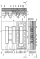
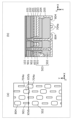
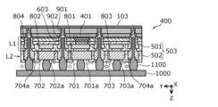
- FIG. 1 is a diagram showing the configuration of a power amplification semiconductor device 100 according to the first embodiment.
- 1A shows a plan view of the power amplification semiconductor device 100
- FIG. 1(c) shows a cross-sectional view of the power amplifying semiconductor device 100 according to the first embodiment, taken along the Ic-Ic cutting line in FIG. 1(a). .
- the power amplification semiconductor device 100 is a semiconductor device (semiconductor chip) that operates at a high frequency and includes a plurality of unit HEMTs (High Electron Mobility Transistors) connected in parallel.
- High frequency means, for example, a frequency of 3 GHz or higher, but is not limited thereto.
- High frequency refers to radio waves, and includes, for example, millimeter waves and electromagnetic waves.
- each unit HEMT includes one source electrode 301 (finger electrode), one drain electrode 302 (finger electrode), and one gate electrode 303 (finger electrode).
- the power amplification semiconductor device 100 includes a substrate 101, a semiconductor epitaxial layer 102, a first insulating layer 201, a second insulating layer 202, and a third insulating layer.
- the unit HEMT is A connection layer L1 including a source electrode 301, a drain electrode 302, and a gate electrode 303, which constitute the same, is formed. Further, in this embodiment, the metal layer formed on the fifth insulating layer 205 provided on the connection layer L1 connects to the source electrode 301, the drain electrode 302, and the gate electrode 303 through a part of the wiring layer, respectively.
- a terminal layer L2 including a source pad 701a, a drain pad 702a, and a gate pad 703a is formed.
- the substrate 101 is, for example, a substrate made of Si.
- a semiconductor epitaxial layer 102 is formed on the first main surface (front surface) of the substrate 101, and a back electrode 103 is formed on the second main surface (back surface) opposite to the first main surface.
- the substrate 101 is not limited to a substrate made of Si, but may be a substrate made of sapphire, SiC, GaN, AlN, or the like.
- the semiconductor epitaxial layer 102 is formed on the surface of the substrate 101 and is a layer for forming a plurality of unit HEMTs.
- the semiconductor epitaxial layer 102 can also be said to be a layer including a plurality of unit HEMTs.
- the semiconductor epitaxial layer 102 is an example of a semiconductor layer.
- the semiconductor epitaxial layer 102 is, for example, a nitride semiconductor layer having a thickness of 2 ⁇ m and having a multilayer structure of AlN and AlGaN.
- the semiconductor epitaxial layer 102 has within the layer a two-dimensional electron gas layer (not shown) that serves as a carrier for a transistor. Carriers in the transistor may be formed by ion implantation or doping according to epitaxial layer formation conditions. Further, the semiconductor epitaxial layer 102 may be made of other semiconductor materials such as GaN, InGaN, InAlGaN, Si, SiC, GaAs, AlGaAs, InGaAs, InP, and InN.
- the back electrode 103 is provided on the back surface of the substrate 101 and is set to the same source potential as the source electrode 301.
- the back electrode 103 is an electrode in the form of a solid pattern (uniformly continuous planar (ie, solid) pattern with substantially no gaps) that covers the back surface of the substrate 101, and covers, for example, the entire area on the back surface side.
- the back electrode 103 may be, for example, any one of Ti, Al, W, Ta, Cu, Ni, Au, Sn, Ag, or an alloy containing at least one of them.
- the back electrode 103 may be a single-layer electrode film having a single-layer structure, or may be a multi-layer electrode film having a laminate structure in which a plurality of metal layers are laminated. Note that being set to the source potential means that the source potential is supplied.
- a first insulating layer 201 is formed on the semiconductor epitaxial layer 102 .
- the first insulating layer 201 is made of SiN with a thickness of 30 nm, for example. Note that the first insulating layer 201 may be configured to include at least one of SiN, SiO 2 , SiON, SiC, C (diamond), AlN, and Al 2 O 3 .
- the source electrode 301 and the drain electrode 302 are provided facing each other on the semiconductor epitaxial layer 102 through an opening in the first insulating layer 201.
- the source electrode 301 and the drain electrode 302 are, for example, multilayer electrode films having a laminated structure in which a Ti film and an Al film are sequentially laminated, but are not limited thereto.
- the source electrode 301 and the drain electrode 302 may be made of, for example, any one of Ti, Al, Ni, Au, Ta, W, Pd, Cu, etc., or an alloy containing at least one of them. Further, the source electrode 301 and the drain electrode 302 may be a single-layer electrode film having a single-layer structure.
- source electrode 301 and the drain electrode 302 are electrically ohmically connected to a carrier of a transistor formed in the semiconductor epitaxial layer 102.
- drain electrodes 302 are provided corresponding to the unit HEMT.
- the gate electrode 303 is provided on the semiconductor epitaxial layer 102 and between the source electrode 301 and the drain electrode 302.
- the gate electrode 303 is, for example, a multilayer electrode film having a laminated structure in which a Ni film and an Au film are laminated in order, but the present invention is not limited thereto.
- the gate electrode 303 may be made of, for example, any one of Ti, TiN, Ta, TaN, W, Ni, Pd, Au, Al, Cu, or an alloy containing at least one of them.
- the gate electrode 303 may be a single-layer electrode film having a single-layer structure.
- the gate electrode 303 has a function of controlling the current flowing between the source electrode 301 and the drain electrode 302 with respect to the carriers formed in the semiconductor epitaxial layer 102 by the voltage or current applied to the gate electrode 303.
- a Schottky junction type in which the first insulating layer 201 is opened, or a metal-insulator-semiconductor so-called MIS structure in which the first insulating layer 201 is not opened may be formed.
- a plurality of gate electrodes 303 are provided corresponding to the unit HEMT.
- the second insulating layer 202 is provided on the source electrode 301, the drain electrode 302, and the gate electrode 303, and is made of SiN or SiO 2 with a thickness of 150 nm, for example. Note that the second insulating layer 202 may be configured to include at least one of SiN, SiO 2 , SiON, SiC, C (diamond), AlN, and Al 2 O 3 .
- the field plate electrode 304 is formed on the second insulating layer 202 and is located closer to the drain electrode 302 (on the X-axis positive side) than the source electrode 301 side end of the gate electrode 303 in a plan view. It is provided parallel to the long side direction (Y-axis direction) of 303.
- the field plate electrode 304 is, for example, a multilayer electrode film having a laminated structure in which a Ti film and an Al film are laminated in order, but the present invention is not limited thereto.
- the field plate electrode 304 may be made of, for example, any one of Ti, TiN, Ta, TaN, W, Ni, Pd, Au, Al, Cu, etc., or an alloy containing at least one of them.
- the field plate electrode 304 may be a single-layer electrode film having a single-layer structure.
- field plate electrode 304 is connected to have the same potential as the source electrode 301 in FIG. 1, it may be connected to have the same potential as the gate electrode 303.
- the third insulating layer 203 is provided on the field plate electrode 304 and is made of SiN or SiO 2 with a thickness of 300 nm, for example. Note that the third insulating layer 203 may be configured to include at least one of SiN, SiO 2 , SiON, SiC, C (diamond), AlN, and Al 2 O 3 .
- the first wiring layer 501 is provided on the third insulating layer 203 and is a metal layer that connects each electrode.
- the first wiring layer 501 is, for example, a multilayer electrode film having a laminated structure in which a Ti film and an Al film are sequentially laminated, but the present invention is not limited thereto.
- the first wiring layer 501 may be made of at least one of Al, Au, Cu, Ti, W, Ta, and the like.
- the electrode-wiring opening connection portion 601 includes the source electrode 301 and the first wiring layer 501, the drain electrode 302 and the first wiring layer 501, the gate electrode 303 and the first wiring layer 501, and the field plate electrode 304 and the first wiring layer 501. , the second insulating layer 202 and the third insulating layer 203 are opened for connection.
- the fourth insulating layer 204 is provided on the first wiring layer 501, and is made of, for example, SiN or SiO 2 with a thickness of several ⁇ m (for example, 1 ⁇ m).
- the fourth insulating layer 204 may include at least one of SiN, SiO 2 , SiON, SiC, C (diamond), AlN, and Al 2 O 3 .
- the second wiring layer 502 is provided on the fourth insulating layer 204, and is, for example, a multilayer electrode film having a laminated structure in which a Ti film and an Al film are sequentially laminated, but is not limited thereto.
- the second wiring layer 502 may be made of at least one of Al, Au, Cu, Ti, W, Ta, and the like.
- the second wiring layer 502 may be made of the same metal as the first wiring layer 501, or may be made of a different metal from the second wiring layer 502.
- the wiring-to-wiring opening connection portion 602 is an opening in the fourth insulating layer 204 for connection between the first wiring layer 501 and the second wiring layer 502.
- the source aggregation unit 701 aggregates the potential of the source electrode 301 in the first wiring layer 501 and the second wiring layer 502 via the electrode-to-wiring opening connection portion 601 and the wiring-to-wiring opening connection portion 602. be.
- a plurality of source electrodes 301 are collectively connected and wired. That is, the source aggregation unit 701 is electrically connected to each of the plurality of source electrodes 301 and can supply the same potential to each of the plurality of source electrodes 301.
- the source aggregation section 701 includes an electrode-to-wiring opening connection section 601 and a wiring-to-wiring opening connection section 602 in the first wiring layer 501 and the second wiring layer 502 in the active region 401.
- the source electrode 301 and the field plate electrode 304 are integrated through the electrode.
- the source aggregation section 701 has a source pad 701a provided on the connection layer L1 and connected to the source electrode 301, the drain electrode 302, and the gate electrode 303 through a part of the wiring layer, respectively.
- the source pad 701a is a portion of the source aggregation portion 701 that is exposed through the source bump opening 801, which is an opening formed in the fifth insulating layer 205. This is the part that is electrically connected to the mounting board or semiconductor package outside the chip.
- the drain aggregation section 702 aggregates the potential of the drain electrode 302 in the first wiring layer 501 and the second wiring layer 502 via the electrode-wiring opening connection section 601 and the wiring-wiring opening connection section 602. be.
- a plurality of drain electrodes 302 are collectively connected and wired in a part of the wiring layer. That is, the drain aggregation section 702 is electrically connected to each of the plurality of drain electrodes 302, and can supply the same potential to each of the plurality of drain electrodes 302.
- the drain concentration section 702 connects the first wiring layer 501 and the first wiring layer 501 in the inactive region 402 in a direction (Y-axis direction) parallel to the long side direction of the gate electrode 303 in the active region 401 from the source concentration section 701.
- the drain electrodes 302 are aggregated via an electrode-to-wiring opening connection portion 601 and a wiring-to-wiring opening connection portion 602.
- the drain aggregation section 702 has a drain pad 702a provided on the connection layer L1 and connected to the source electrode 301, the drain electrode 302, and the gate electrode 303 through a part of the wiring layer, respectively.
- the drain pad 702a is a portion of the drain aggregation portion 702 that is exposed through the drain bump opening 802, which is an opening formed in the fifth insulating layer 205. This is the part that is electrically connected to the mounting board outside the chip.
- the gate aggregation section 703 aggregates the potential of the gate electrode 303 in the first wiring layer 501 and the second wiring layer 502 via the electrode-wiring opening connection section 601 and the wiring-wiring opening connection section 602. be.
- a plurality of gate electrodes 303 are collectively connected and wired in a part of the wiring layer.
- the gate aggregation section 703 is electrically connected to each of the plurality of gate electrodes 303, and can supply the same potential to each of the plurality of gate electrodes 303.
- the gate aggregation section 703 has a first interconnection layer 501 and a second interconnection layer 502 between the electrode and the interconnection.
- Gate electrodes 303 are aggregated via an opening connection portion 601 and an opening connection portion 602 between wirings.
- the gate aggregation section 703 has a gate pad 703a provided on the connection layer L1 and connected to the source electrode 301, the drain electrode 302, and the gate electrode 303 through a part of the wiring layer, respectively.
- the gate pad 703a is a portion of the gate aggregation portion 703 that is exposed through the gate bump opening 803, which is an opening formed in the fifth insulating layer 205. This is the part that is electrically connected to the mounting board outside the chip.
- source aggregation section 701, the drain aggregation section 702, and the gate aggregation section 703 have a rectangular shape in plan view, they are not limited to this.
- the fifth insulating layer 205 is provided on the second wiring layer 502, and is made by laminating, for example, an organic resin film with a thickness of 6 ⁇ m on SiN with a thickness of 800 nm. Note that the fifth insulating layer 205 may be configured to include at least one of SiN, SiO 2 , SiON, SiC, C (diamond), AlN, and Al 2 O 3 .
- the fifth insulating layer 205 has a source bump opening 801 in which the fifth insulating layer 205 is opened to expose the source concentrated portion 701, and a drain bump opening 801 in which the fifth insulating layer 205 is opened to expose the drain concentrated portion 702.
- a bump opening 802 and a gate bump opening 803 are formed by opening the fifth insulating layer 205 and exposing the gate aggregation portion 703.
- the shield wiring layer 503 functions as a shield (electromagnetic shield) against noise, and is composed of a first wiring layer 501 and a second wiring layer 502.
- the shield wiring layer 503 is a wiring layer having the same potential as the source electrode 301.
- the shield wiring layer 503 is provided at the position of the connection layer in the direction perpendicular to the surface of the substrate 101 (Z-axis direction) so as to surround at least one of the drain aggregation section 702 and the gate aggregation section 703 in plan view. Further, the shield wiring layer 503 is provided so as to surround at least one of the drain pad 702a and the gate pad 703a in plan view.
- the via-wiring opening connection portion 603 connects the first wiring layer 501 and the semiconductor layer via 902 by opening the first insulating layer 201, the second insulating layer 202, and the third insulating layer 203.
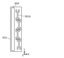
- the shield bump opening 804 is a part that opens the fifth insulating layer 205 to expose the shield wiring layer 503, and the bump metal placed in the shield bump opening 804 connects the ground potential of the mounting board outside the chip. This is the point for electrical connection.
- Substrate via 901 is arranged so as to surround (for example, four sides) at least one of drain concentration section 702 and gate concentration section 703 in plan view. It is arranged so as to surround the aggregation section 703.
- the substrate via 901 is a through hole that opens the substrate 101 and reaches the back electrode 103, and connects the shield wiring layer (for example, the first wiring layer 501 and the second wiring layer 501) that is part of the wiring layer set to the source potential. (at least one of the wiring layers 502) on the inner wall.
- the shape of the substrate via 901 in plan view is, for example, a rectangle, but is not limited thereto. Further, for example, a plurality of substrate vias 901 are arranged.
- the substrate vias 901 under the shield wiring layer 503 are arranged discontinuously.
- the opening contour of the substrate via 901 has a discontinuous portion 911 .
- the substrate vias 901 are not arranged so as to continuously surround the gate aggregation section 703.
- substrate vias 901 and discontinuous portions 911 are alternately arranged. Note that at least one discontinuous portion 911 may be provided.
- Semiconductor layer via 902 is arranged so as to surround at least one of drain concentration section 702 and gate concentration section 703 in plan view, and in this embodiment, it penetrates semiconductor epitaxial layer 102 and connects shield wiring layer 503. have on the inner wall.
- the semiconductor layer via 902 is a through hole that opens the semiconductor epitaxial layer 102 and reaches the substrate 101.
- the semiconductor layer via 902 is formed in an annular shape surrounding the gate aggregation portion 703. Further, for example, a plurality of semiconductor layer vias 902 are arranged.
- the power amplification semiconductor device 100 configured as described above includes an active region 401 having a two-dimensional electron gas layer formed in the semiconductor epitaxial layer 102, and an inactive region 402 having no two-dimensional electron gas layer. It is divided into.
- the active region 401 is a region (a region on the substrate 101) where a two-dimensional electron gas layer exists in plan view.
- a HEMT high frequency amplification amplifier
- a HEMT high frequency amplification amplifier including at least a source electrode 301, a drain electrode 302, and a gate electrode 303 is formed in the active region 401.
- the non-active region 402 is a region on the substrate 101 outside the active region 401, and is a region where no two-dimensional electron gas layer exists.
- Non-active region 402 may be formed, for example, by implanting molecules containing any of He, B, H, F, and Fe. Note that the absence of a two-dimensional electron gas layer includes not only the complete absence of electrons but also the substantial absence of electrons.
- the power amplification semiconductor device 100 is a power amplification semiconductor device that operates at a frequency of 3 GHz or higher, in which a plurality of unit HEMTs (High Electron Mobility Transistors) are connected in parallel.
- a semiconductor epitaxial layer 102 (an example of a semiconductor layer) provided on the surface of the substrate 101 and including a plurality of unit HEMTs, and a source electrode 301, drain electrode 302, and gate provided on the semiconductor epitaxial layer 102 and including a plurality of unit HEMTs.
- connection layer L1 including an electrode 303; a source pad 701a, a drain pad 702a, and A terminal layer L2 including a gate pad 703a, a back electrode 103 provided on the back surface of the substrate 101 and set to the same source potential as the source electrode 301, and a wiring penetrating the substrate 101 and set to the source potential.
- a substrate via 901 having a shield wiring layer 503, which is a second part of the layer, is provided on the inner wall.
- drain aggregation part 702 in which a plurality of gate electrodes 303 are collectively connected and wired in a third part of the wiring layer
- gate aggregation part 703 in which a plurality of gate electrodes 303 are collectively connected and wired in a fourth part of the wiring layer.
- one or both of the drain aggregation section 702 and the gate aggregation section 703 are surrounded by substrate vias 901 .
- the substrate vias 901 are arranged to surround the gate aggregation section 703, noise transmitted through the substrate 101 and received by the gate aggregation section 703 can be suppressed. Furthermore, when the substrate vias 901 are arranged so as to surround the drain collecting section 702, it is possible to suppress the noise transmitted through the substrate 101 and radiated from the drain collecting section 702, and the noise is transmitted to the gate collecting section 703. Alternatively, noise radiation to components outside the power amplification semiconductor device 100 can be suppressed. Therefore, the power amplification semiconductor device 100 can suppress the influence of noise signals more than before.
- a semiconductor layer via 902 that penetrates the semiconductor epitaxial layer 102 and has a shield wiring layer 503 on an inner wall, and in plan view, one or both of the drain concentration section 702 and the gate concentration section 703 are formed in the semiconductor layer. It may be surrounded by vias 902.
- the semiconductor layer via 902 when the semiconductor layer via 902 is arranged so as to surround the gate aggregation section 703, noise transmitted through the semiconductor epitaxial layer 102 and received by the gate aggregation section 703 can be suppressed. Further, when the semiconductor layer via 902 is arranged so as to surround the drain aggregation section 702, it is possible to suppress the noise transmitted through the semiconductor epitaxial layer 102 and radiated from the drain aggregation section 702, and the noise to the gate aggregation section 703 can be suppressed. Noise transmission or noise radiation to components outside the power amplification semiconductor device 100 can be suppressed. Therefore, the power amplification semiconductor device 100 can suppress the influence of noise signals more than before.
- one or both of the drain concentration section 702 and the gate concentration section 703 is surrounded by the shield wiring layer 503 in plan view. Good too.
- the shield wiring layer 503 when the shield wiring layer 503 is arranged to surround the gate aggregation section 703, it is possible to suppress noise transmitted from the first insulating layer 201 through the fourth insulating layer 204 and received by the gate aggregation section 703. can. Furthermore, when the shield wiring layer 503 is arranged so as to surround the drain aggregation section 702, it is possible to suppress noise transmitted from the first insulating layer 201 to the fourth insulating layer 204 and radiated from the drain aggregation section 702. Therefore, it is possible to suppress noise transmission to the gate aggregation unit 703 or noise radiation to components outside the power amplification semiconductor device 100. Therefore, the power amplification semiconductor device 100 can further suppress the influence of noise signals than before.
- either or both of the drain pad 702a and the gate pad 703a may be surrounded by the shield wiring layer 503.
- the shield bump opening 804 when the shield bump opening 804 is arranged so as to surround the gate aggregation part 703, the bump metal arranged in the shield bump opening 804 surrounds the gate aggregation part 703, and therefore passes through the fifth insulating layer 205.
- the bump metal arranged in the shield bump opening 804 surrounds the drain collecting part 702, so that it does not pass through the fifth insulating layer 205.
- noise emitted from the drain aggregation section 702 can be suppressed, and noise transmission to the gate aggregation section 703 or noise emission to components outside the power amplification semiconductor device 100 can be suppressed. Therefore, the power amplification semiconductor device 100 can further suppress the influence of noise signals than before.
- the opening contour of the substrate via 901 may have a discontinuous portion 911 (an example of a first discontinuous portion).
- the substrate vias 901 under the shield wiring layer 503 are disposed discontinuously, so when the substrate vias 901 surround the gate aggregation section 703 or the drain aggregation section 702, the gate aggregation section 703 and the drain aggregation section 702 are Falling off from the substrate 101 can be prevented.
- FIG. 2 is a plan view showing an example of the arrangement of substrate vias 901 and semiconductor layer vias 902 in a power amplification semiconductor device according to a modification of the first embodiment.
- the power amplification semiconductor device according to this modification differs from the power amplification semiconductor device 100 according to the first embodiment in the arrangement of semiconductor layer vias 902.
- the semiconductor layer vias 902 under the shield wiring layer 503 are arranged discontinuously like the substrate vias 901.
- the opening contour of the semiconductor layer via 902 has a discontinuous portion 912 .
- the semiconductor layer vias 902 are not arranged so as to continuously surround the gate aggregation section 703.
- the semiconductor layer vias 902 and the substrate vias 901 may correspond to each other, and the discontinuous portions 912 and 911 may correspond to each other.
- the semiconductor layer via 902 and the substrate via 901 may be arranged so that at least a portion thereof overlaps, and the discontinuous portion 912 and the discontinuous portion 911 may at least partially overlap.
- the opening outline of the semiconductor layer via 902 has a discontinuous portion 912 (an example of a second discontinuous portion).
- the gate aggregation section 703 and the drain aggregation section 702 are arranged discontinuously, bumps such as ball bumps that cannot be arranged in a continuous pattern can be used.
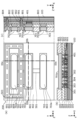
- FIG. 3 is a diagram showing the configuration of a power amplification semiconductor device 200 according to the second embodiment.
- FIG. 3(a) shows a plan view of the power amplification semiconductor device 200
- FIG. 3C shows a cross-sectional view of the power amplification semiconductor device 200 according to the second embodiment, taken along the line IIIc-IIIc in FIG. 3A.
- power amplification semiconductor device 200 differs from power amplification semiconductor device 100 according to the first embodiment in that it is arranged so as to surround drain aggregation section 702 .
- the power amplification semiconductor device 200 includes a back electrode 103 formed on the back surface of the substrate 101 and a substrate 101 arranged so as to surround the drain concentration portion 702 in the inactive region 402.
- a via-to-wiring opening connecting portion 603 that connects the first wiring layer 501 and the semiconductor layer via 902 through an opening, and a shield wiring layer composed of the first wiring layer 501 and the second wiring layer 502. 503, and a shield bump opening 804 in which the fifth insulating layer 205 is opened to expose the shield wiring layer 503.
- the substrate via 901, the semiconductor layer via 902, and the shield wiring layer 503 may be arranged so as to surround the drain concentration section 702 in plan view. Note that at least one of the substrate via 901, the semiconductor layer via 902, and the shield wiring layer 503 may be arranged so as to surround the drain concentration section 702.
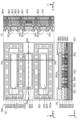
- FIG. 4 is a diagram showing the configuration of a power amplification semiconductor device 300 according to the third embodiment.
- 4(a) shows a plan view of the power amplifying semiconductor device 300
- FIG. 4(c) shows a cross-sectional view of the power amplifying semiconductor device 300 according to the third embodiment, taken along the IVc-IVc cutting line in FIG. 4(a).
- power amplification semiconductor device 300 differs from power amplification semiconductor device 100 according to the first embodiment in that substrate vias 901 and the like are arranged to surround each of drain aggregation section 702 and gate aggregation section 703.
- the power amplification semiconductor device 300 is arranged so as to surround the back electrode 103 formed on the back surface of the substrate 101 and the gate aggregation section 703 and the drain aggregation section 702 in the inactive region 402.
- a substrate via 901 that opens the substrate 101 and reaches the back electrode 103
- a semiconductor layer via 902 that opens the semiconductor epitaxial layer 102 and reaches the substrate 101
- the first insulating layer 201 and the second insulating layer 202 The via-to-wiring opening connecting portion 603 connects the first wiring layer 501 and the semiconductor layer via 902 by opening the third insulating layer 203, and the first wiring layer 501 and the second wiring layer 502.
- the fifth insulating layer 205 is opened to expose the shield wiring layer 503, and a shield bump opening 804 is provided.
- the substrate via 901, the semiconductor layer via 902, and the shield wiring layer 503 may be arranged to surround each of the drain aggregation section 702 and the gate aggregation section 703 in a plan view. Note that at least one of the substrate via 901, the semiconductor layer via 902, and the shield wiring layer 503 may be arranged so as to surround the drain aggregation section 702 and the gate aggregation section 703.
- the drain aggregation section 702 and the gate aggregation section 703 may be surrounded by the substrate via 901 in plan view.
- the substrate vias 901 are arranged so as to surround the drain aggregation section 702 and the gate aggregation section 703, thereby suppressing noise reception to the gate aggregation section 703 through the substrate 101 and suppressing noise reception from the drain aggregation section 702. It is also possible to suppress noise emission. Suppression of noise emission leads to suppression of noise emission to components outside the power amplification semiconductor device 300.
- drain aggregation section 702 and the gate aggregation section 703 may be surrounded by the semiconductor layer via 902.
- the semiconductor layer via 902 is arranged so as to surround the drain aggregation section 702 and the gate aggregation section 703, so that noise transmitted through the semiconductor epitaxial layer 102 can be suppressed from being received to the gate aggregation section 703, and the drain aggregation section 702 can be suppressed.
- drain aggregation section 702 and the gate aggregation section 703 may be surrounded by the shield wiring layer 503.
- the shield wiring layer 503 is arranged so as to surround the gate aggregation section 703 and the drain aggregation section 702, so that the noise transmitted from the first insulating layer 201 to the fourth insulating layer 204 is transmitted to the gate aggregation section 703. and noise emission from the drain aggregation section 702 can be realized.
- drain pad 702a and the gate pad 703a may be surrounded by the shield wiring layer 503.
- the shield bump opening 804 is arranged so as to surround the gate collecting part 703 and the drain collecting part 702, so that the bump metal arranged in the shield bump opening 804 surrounds the gate collecting part 703 and the drain collecting part 702. Therefore, it is possible to suppress noise reception to the gate aggregation section 703 and suppression of noise emission from the drain aggregation section 702 by transmitting through the fifth insulating layer 205.
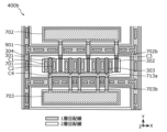
- FIG. 5 is a diagram showing the configuration of a power amplification semiconductor device 400 according to a modification of the third embodiment.
- 5(a) shows a plan view of the power amplification semiconductor device 400
- FIG. 5(b) shows a modification of the third embodiment, cut along the Vb-Vb cutting line in FIG. 5(a).
- FIG. 5(c) shows a cross-sectional view of a power amplifying semiconductor device 400 according to a modification of the third embodiment, cut along the Vc-Vc cutting line in FIG. 5(a). 400 is shown in cross section.
- the power amplification semiconductor device 400 is the power amplification semiconductor device according to the third embodiment in that, in addition to the drain aggregation section 702 and the gate aggregation section 703, a substrate via 901 and the like are arranged so as to surround the source aggregation section 701. It is different from 300.
- the substrate via 901, the semiconductor layer via 902, and the shield wiring layer 503 may be arranged to surround each of the source aggregation section 701, the drain aggregation section 702, and the gate aggregation section 703 in plan view. good.
- FIG. 6 is a plan view showing the configuration of a power amplification semiconductor device 500 according to the fourth embodiment.
- FIG. 7 is a plan view showing an example of arrangement of substrate vias 901 and semiconductor layer vias 902 in power amplification semiconductor device 500 according to the fourth embodiment.
- the power amplification semiconductor device 500 differs from the power amplification semiconductor device 400 according to the modification of the third embodiment in that each of the substrate vias 901 and the semiconductor layer vias 902 are formed in duplicate. Note that an example of the arrangement of substrate vias 901 and semiconductor layer vias 902 according to this embodiment will be described below using a power amplification semiconductor device 400 according to a modification of Embodiment 3; The arrangement example of the substrate via 901 and the semiconductor layer via 902 according to this embodiment can also be applied to each modification.
- the power amplification semiconductor device 500 is arranged such that a plurality of substrate vias 901 form two or more substrate via rows in plan view.
- the four-sided enclosure by the substrate vias 901 in each of the source aggregation section 701, the drain aggregation section 702, and the gate aggregation section 703 can be said to be a multi-row enclosure.
- the two or more substrate via rows include a first substrate via row 921a and a second substrate via row 921b. Note that the number of substrate via rows may be three or more. Further, like the substrate vias 901, the semiconductor layer vias 902 are also arranged so that a plurality of semiconductor layer vias 902 form two or more semiconductor layer via rows in plan view.
- the first substrate via row 921a and the second substrate via row 921b are arranged from an outer position (for example, a position on the negative side of the and the center position of the gate aggregation portion 703), the discontinuous portions 911a and 911b of each via row are arranged so as not to overlap with each other.
- the substrate vias 901 of the first substrate via row 921a and the second substrate via row 921b are arranged alternately (in a zigzag shape). It can also be said that the substrate vias 901 under the shield wiring layer 503 are arranged discontinuously and alternately in multiples.
- the substrate vias 901 of the first substrate via array 921a and the second substrate via array 921b are arranged so as to partially overlap in the direction in which the via arrays are arranged (in the example of FIG. 7, the X-axis direction).
- the length of the substrate via 901 in the Y-axis direction may be longer than the length of the discontinuous portions 911a and 911b in the Y-axis direction.
- the first semiconductor layer via array 922a and the second semiconductor layer via array 922b are arranged from an outer position (for example, a position on the negative side of the 702 and the center position of the gate aggregation portion 703), the discontinuous portions 912a and 912b of each via row are arranged so as not to overlap each other.
- the semiconductor layer vias 902 of the first semiconductor layer via array 922a and the second semiconductor layer via array 922b are arranged alternately (in a zigzag shape). Furthermore, it can be said that the semiconductor layer vias 902 are arranged discontinuously and alternately in multiples.
- the semiconductor layer vias 902 of the first semiconductor layer via array 922a and the second semiconductor layer via array 922b are arranged such that they partially overlap in the direction in which the via arrays are arranged (in the example of FIG. 7, the X-axis direction).
- the length of the semiconductor layer via 902 in the Y-axis direction may be longer than the length of the discontinuous portions 912a and 912b in the Y-axis direction.
- the shield bump openings 804 may also be arranged discontinuously and alternately in multiples.
- the power amplification semiconductor device 400 according to the fourth embodiment is surrounded by the substrate vias 901 arranged in multiple rows in plan view, and the outer position of the substrate vias 901 arranged in the multiple rows is
- the substrate vias 901 included in the multiple rows are arranged so that the discontinuous parts 911a and 911b (an example of the first discontinuous part) of each row do not overlap each other when looking at the internal center position from the inside.
- the substrate vias 901 under the shield wiring layer 503 are arranged discontinuously and alternately in multiple layers, which has the effect of suppressing noise from leaking out or entering from gaps between the discontinuous substrate vias 901. be.
- the periphery is surrounded by semiconductor layer vias 902 arranged in multiple rows, and when looking from the outer position to the inner center position of the semiconductor layer vias 902 arranged in multiple rows, each row
- the semiconductor layer vias 902 included in the multiple rows may be arranged so that the discontinuous parts 912a and 912b (an example of the second discontinuous part) do not overlap with each other.
- the shield bump openings 804 are arranged discontinuously, multiplexed, and staggered, so that noise leaks from the gaps between the bump metals arranged inside the discontinuous shield bump openings 804. It has the effect of inhibiting entry.
- FIGS. 8A and 8B are plan views showing examples of arrangement of substrate vias and semiconductor layer vias in a power amplification semiconductor device according to a modification of the fourth embodiment.
- the plan view shape (the shape of the opening outline) of the substrate via 901a has one or more bent portions 901a1, which are bent portions.
- the substrate via 901a has a portion that is parallel to the arrangement direction (in the example of FIG. 8A, the Y-axis direction) of the substrate vias 901a included in the substrate via row, and a portion that is bent with respect to the arrangement direction. It may be formed by combining.
- the bent portion 901a1 is bent in a direction intersecting (for example, orthogonal to) the parallel portion in plan view, and toward the other substrate via array side.
- the bent portion 901a1 of the substrate via 901a included in the first substrate via array 921a is bent toward the second substrate via array 921b (in the example of FIG. 8A, the X-axis positive side).
- the bent portion 901a1 is bent from the ends (for example, both ends) of the parallel portion toward the other substrate via rows. Furthermore, the bent portions 901a1 of the substrate vias 901a included in the first substrate via array 921a and the bent portions 901a1 of the substrate vias 901a included in the second substrate via array 921b are at least partially opposed to each other.
- plan view shape of the substrate via 901a included in the first substrate via row 921a and the plan view shape of the substrate via 901a included in the second substrate via row 921b are, for example, point-symmetric shapes.
- the plan view shape (the shape of the opening outline) of the semiconductor layer via 902a has one or more bent portions 902a1, which are bent portions, similarly to the substrate via 901a.
- the semiconductor layer via 902a has a portion parallel to the arrangement direction (in the example of FIG. 8A, the Y-axis direction) of the semiconductor layer via 902a included in the semiconductor layer via array, and a portion bent with respect to the arrangement direction. It may be formed by combining the parts.
- the bent portion 902a1 is bent in a direction intersecting the parallel portion in a plan view and toward the other semiconductor layer via array side.
- the bent portion 902a1 of the semiconductor layer via 902a included in the second semiconductor layer via array 922b is bent toward the second semiconductor layer via array 922b (in the example of FIG. 8A, the X-axis plus side).
- the bent portion 902a1 is bent from the ends (for example, both ends) of the parallel portion toward the other semiconductor layer via array side. Further, the bent portion 902a1 of the semiconductor layer via 902a included in the first semiconductor layer via array 922a and the bent portion 902a1 of the semiconductor layer via 902a included in the second semiconductor layer via array 922b are at least partially opposed to each other.
- plan view shape of the semiconductor layer via 902a included in the first semiconductor layer via array 922a and the plan view shape of the semiconductor layer via 902a included in the second semiconductor layer via array 922b are, for example, point-symmetric shapes. be.
- the substrate via 901a and the semiconductor layer via 902a have corresponding shapes (shapes with bent portions) and are arranged so that at least a portion thereof overlaps in a plan view.
- the plan view shape (the shape of the opening outline) of the substrate via 901b has one or more branched portions 901b1.
- the substrate vias 901b are arranged in a portion parallel to the direction in which the substrate vias 901b included in the substrate via row are arranged (Y-axis direction in the example of FIG. 8B) and branched from both ends of the parallel portion.
- the branch portion 901b1 may be formed in combination with the branch portion 901b1 that protrudes from the side.
- the branching portion 901b1 branches into a Y-shape from the ends (for example, both ends) of the parallel portion in plan view. Furthermore, at least a portion of the branch portion 901b1 of the substrate via 901b included in the first substrate via array 921a and the branch portion 901b1 of the substrate via 901b included in the second substrate via array 921b face each other.
- the plan view shape (the shape of the opening outline) of the semiconductor layer via 902b has one or more branch portions 902b1, which are branched portions, similarly to the substrate via 901b.
- the semiconductor layer via 902b has a portion parallel to the arrangement direction (in the example of FIG. 8A, the Y-axis direction) of the semiconductor layer via 902b included in the semiconductor layer via array, and a portion from both ends of the parallel portion. It may be formed in combination with a branch portion 902b1 that protrudes to branch.
- the branch portion 902b1 protrudes in a Y-shape from the ends (for example, both ends) of the parallel portion in plan view. Further, the branch portion 902b1 of the semiconductor layer via 902b included in the first semiconductor layer via array 922a and the branch portion 902b1 of the semiconductor layer via 902b included in the second semiconductor layer via array 922b are at least partially opposed to each other.
- the opening contours of the substrate vias 901a and 901b have a plurality of bent portions 901a1 or a plurality of branch portions 901b1 in plan view.
- the opening contours of the semiconductor layer vias 902a and 902b may have a plurality of bent portions 902a1 or a plurality of branched portions 902b1.
- the effect of suppressing noise leakage or noise leakage can be enhanced by a combination of bending patterns or a combination of branching patterns.
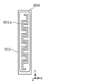
- FIG. 9 is a plan view showing an example of the arrangement of substrate vias 901 and shield bump openings 804 in the power amplification semiconductor device according to the fifth embodiment.
- the substrate vias 901 under the shield wiring layer 503 are arranged discontinuously and alternately in multiples
- the shield bump openings 804 are arranged discontinuously and alternately in multiples.
- the power amplification semiconductor device according to the fifth embodiment in addition to the power amplification semiconductor device 500 according to the fourth embodiment, is arranged alternately (in a zigzag shape) in each of the first substrate via row 921a and the second substrate via row 921b.
- a shield bump opening 804 is provided.
- the arrangement interval of the substrate vias 901 and the arrangement interval of the shield bump openings 804 are different. Therefore, in plan view, there are a region where only the substrate via 901 is arranged, a region where only the shield bump opening 804 is arranged, and a region where both the substrate via 901 and the shield bump opening 804 overlap.
- the shield wiring layer 503 that surrounds either or both of the drain aggregation section 702 and the gate aggregation section 703 has a structure in which the shield interconnection layer 503 is continuously arranged between the terminal layer L2 and the substrate 101 in plan view. and a second region R2 in which the shield wiring layer 503 is not continuously arranged.
- FIG. 10 is a cross-sectional view of the power amplification semiconductor device according to the fifth embodiment along each cutting line in FIG. 9.
- 10(a) is a cross-sectional view of the power amplification semiconductor device according to the fifth embodiment, taken along the Xa-Xa cutting line shown in FIG. 10 is a sectional view of the power amplifying semiconductor device according to the fifth embodiment taken along the -Xb cutting line
- (c) of FIG. 10 is a cross-sectional view of the power amplifying semiconductor device according to the fifth embodiment taken along the Xc-Xc cutting line shown in FIG.
- FIG. 2 is a cross-sectional view of such a power amplification semiconductor device.
- a shield wiring layer 503 (specifically, a A first wiring layer 501 and a second wiring layer 502) are arranged continuously, and a shield bump opening 804 is formed in each of the two substrate via rows.
- being arranged continuously means that a metal layer for suppressing noise is formed from the terminal layer L2 to the substrate 101.
- “not arranged continuously” means that a metal layer for suppressing noise is formed in a part between the terminal layer L2 and the substrate 101.
- a shield wiring layer 503 (specifically, A first wiring layer 501 and a second wiring layer 502) are arranged continuously, and a shield bump opening 804 is formed in one of the two substrate via rows.
- a shield wiring layer 503 (specifically Specifically, the first wiring layer 501 and the second wiring layer 502) are arranged consecutively (first region R1 shown in FIG. 10(c)), and the other substrate via of the two substrate via rows In the row, the shield wiring layer 503 (specifically, the second wiring layer 502) is disposed only in the terminal layer (fifth insulating layer 205) between the terminal layer and the substrate 101 (see (FIG. 10)). Second region R2) shown in c). Further, the shield bump opening 804 is formed in the second region R2. In other words, the shield bump opening 804 is formed in a region where the shield wiring layer 503 is not continuously arranged.
- the portion of the second wiring layer 502 exposed by the shield bump opening 804 can be made into a flat surface.
- a power amplification semiconductor device is flip-chip mounted on a mounting board using solder balls or the like, it is possible to prevent the solder balls from being sucked into the vias, resulting in insufficient solder and poor conduction.
- the first region R1 is a region in which the substrate via 901 under the shield wiring layer 503, the semiconductor layer via 902, and the shield bump opening 804 are continuously connected, and the second region R2 In the cross-sectional view, the substrate via 901, the semiconductor layer via 902, and the shield bump opening 804 are discontinuous (for example, the substrate via 901, the semiconductor layer via 902, and the shield bump opening 804 are all formed). It can also be said that it is an area where In the power amplification semiconductor device according to the fifth embodiment, the first region R1 and the second region R2 are arranged so as to coexist.
- the shield wiring layer 503 surrounding one or both of the drain aggregation section 702 and the gate aggregation section 703 has the terminal layer L2 in plan view.
- the substrate 101 there is a region where the shield wiring layer 503 is continuously arranged (for example, the first region R1) and a region where the shield wiring layer 503 is not continuously arranged (for example, the second region R2).
- the substrate vias 901, the semiconductor layer vias 902, and the shield bump openings 804 under the shield wiring layer 503 are arranged so that areas where they are continuously connected and areas where they are discontinuous coexist. Therefore, the effect of suppressing the noise influence by the shield wiring layer 503, the substrate via 901, the semiconductor layer via 902, and the bump metal arranged inside the shield bump opening 804, and the design freedom in the arrangement of the via etc. It is possible to achieve both the effect of facilitating the adjustment of the degree.
- FIGS. 11A to 11D are plan views showing examples of arrangement of substrate vias and shield bump openings 804 in a power amplification semiconductor device according to a first modification of the fifth embodiment.
- the shield bump opening 804 may be formed to include each of the plurality of substrate vias 901a included in two or more substrate via rows.
- the shield bump opening 804 may be formed to include each of the plurality of substrate vias 901b included in two or more substrate via rows.
- the shield bump opening 804 may be arranged alongside two or more substrate via rows including a plurality of substrate vias 901a.
- the shield bump opening 804 may extend in a direction parallel to the direction in which the substrate via array extends (in the example of FIG. 11C, the Y-axis direction).
- the shield bump opening 804 may be arranged alongside two or more substrate via rows including a plurality of substrate vias 901b.
- the shield bump opening 804 may extend in a direction parallel to the direction in which the substrate via array extends (in the example of FIG. 11D, the Y-axis direction).
- the substrate via and the shield bump opening 804 may be arranged to overlap in plan view, or as shown in FIGS. 11C and 11D, the substrate via and the shield bump opening 804 804 may be arranged so as not to overlap in plan view. Even with this arrangement of substrate vias and shield bump openings 804, the same effects as the power amplification semiconductor device according to the fifth embodiment can be achieved.
- FIG. 12 is a diagram showing the configuration of a power amplification semiconductor device according to a second modification of the fifth embodiment.
- FIG. 12A is a plan view showing an example of the arrangement of substrate vias 901 and shield bump openings 804 in a power amplification semiconductor device according to a second modification of the fifth embodiment.
- FIG. 12(b) is a cross-sectional view of the power amplification semiconductor device according to the second modification of the fifth embodiment, taken along the line XIIb-XIIb in FIG. 12(a).
- a substrate via 901 under the shield wiring layer 503 (first wiring layer 501 and second wiring layer 502)
- the shield bump openings 804 are arranged so as not to overlap with the semiconductor layer vias 902 and the semiconductor layer vias 902 .
- a via row in which substrate vias 901 and semiconductor layer vias 902 are arranged side by side, and a bump row in which shield bump openings 804 are arranged side by side, are different from each other.
- one or more via rows and one or more bump rows are each arranged, and in this modification, two each are arranged, but the number is not particularly limited.
- the substrate vias 901 and semiconductor layer vias 902 included in the two via rows are arranged alternately (zigzag shape), and the shield bump openings 804 included in the two bump rows are arranged alternately (zigzag shape). It is located.
- the shield bump opening 804 is arranged so as not to overlap with the substrate via 901 and the semiconductor layer via 902 under the shield wiring layer 503 in plan view, so that the second The surface shape of the wiring layer 502 can be made flat, and the bump process conditions in the subsequent process can be simplified.
- FIG. 13 is a diagram showing the configuration of a power amplification semiconductor device according to a third modification of the fifth embodiment.
- FIG. 13A is a plan view showing an example of the arrangement of substrate vias 901 and shield bump openings 804 in a power amplification semiconductor device according to a third modification of the fifth embodiment.
- FIG. 13(b) is a cross-sectional view of the power amplifying semiconductor device according to the third modification of the fifth embodiment, taken along the line XIIIb-XIIIb in FIG. 13(a).
- FIG. 13 is a diagram showing the configuration of a power amplification semiconductor device according to a third modification of the fifth embodiment.
- FIG. 13A is a plan view showing an example of the arrangement of substrate vias 901 and shield bump openings 804 in a power amplification semiconductor device according to a third modification of the fifth embodiment.
- FIG. 13(b) is a cross-sectional view of the power amplifying semiconductor device according to the third modification of the fifth embodiment, taken along the line
- FIG. 13(c) is a cross-sectional view of the power amplification semiconductor device according to the third modification of the fifth embodiment, taken along the line XIIIc-XIIIc in FIG. 13(a).
- FIG. 13(b) is a cross-sectional view of the position where the shield bump opening 804 is arranged
- FIG. 13(c) is a cross-sectional view of the position where the substrate via 901 is arranged.
- the substrate vias 901 and the shield bump openings 804 may be arranged alternately in a straight line in a plan view. In this case, substrate via 901 and shield bump opening 804 are arranged so as not to overlap each other in plan view.
- the surface shape of the second wiring layer 502 around the shield bump opening 804 can be made flat, and the bump process conditions in the subsequent process can be simplified. It can be done.
- FIG. 14 is a diagram showing the configuration of a power amplification semiconductor device according to a fourth modification of the fifth embodiment.
- FIG. 14A is a plan view showing an example of the arrangement of substrate vias 901 and shield bump openings 804 in a power amplification semiconductor device according to a fourth modification of the fifth embodiment.
- FIG. 14(b) is a cross-sectional view of the power amplifying semiconductor device according to the fourth modification of the fifth embodiment, taken along the line XIVb-XIVb in FIG. 13(a).
- the power amplification semiconductor device has rows in which substrate vias 901 and shield bump openings 804 are alternately arranged in a straight line in the extending direction ( In the example of FIG. 14, there are a plurality of them in the direction perpendicular to the Y-axis direction (in the example of FIG. 14, the X-axis direction). In this case, each of the plurality of substrate vias 901 and the plurality of shield bump openings 804 are arranged so as not to overlap each other in plan view.
- the power amplification semiconductor device includes a shield pad 704a connected to the shield wiring layer 503 (second wiring layer 502).
- the shield pad 704a is a portion of the second wiring layer 502 that is exposed through the shield bump opening 804.
- the pad area of the shield pad 704a (the area of the shield bump opening 804 shown in FIG. 14(a)) is the same as the opening area of the substrate via 901 (the rectangular shape of the substrate via 901 shown in FIG. 14(a)). area) so as not to overlap.
- the power amplification semiconductor device has the shield pad 704a connected to the shield wiring layer 503, and in plan view, the pad area of the shield pad 704a is connected to the substrate via It does not overlap with the opening area of 901.
- the pad area is arranged at a position that does not overlap the opening area in plan view.
- the surface shape of the second wiring layer 502 around the shield bump openings 804 can be made flat. This makes it possible to simplify the bump process conditions in the subsequent process.
- FIG. 15 is a diagram showing the configuration of a power amplification semiconductor device according to a fifth modification of the fifth embodiment.
- FIG. 15A is a plan view showing an example of the arrangement of substrate vias 901 and shield bump openings 804 in a power amplification semiconductor device according to a fifth modification of the fifth embodiment.
- FIG. 15(b) is a cross-sectional view of the power amplification semiconductor device according to the fifth modification of the fifth embodiment, taken along the line XVb-XVb in FIG. 15(a).
- the shield wiring layer 503 when the shield wiring layer 503 is composed of a plurality of layers including a first wiring layer 501 and a second wiring layer 502, in a plan view, the upper second wiring layer 502 and the lower layer They may be arranged to have different widths from one wiring layer 501.
- the shield wiring layer 503 includes a first shield wiring layer (for example, the first wiring layer 501) provided in the connection layer L1 and a second shield wiring layer (for example, the second wiring layer 501) provided in the terminal layer L2. 502).
- the first shield wiring layer and the second shield wiring layer are connected within the fourth insulating layer 204, for example.
- the second wiring layer 502 is a portion of the first wiring layer 501 where the substrate vias 901 and the semiconductor layer vias 902 are not arranged in plan view, that is, a portion of the first wiring layer 501 where the surface on the Z-axis plus side is flat. will be placed in
- the first shield wiring layer and the second shield wiring layer differ in the width of the wiring surrounding either or both of the drain aggregation section 702 and the gate aggregation section 703.
- the wiring width W1 of the wiring in the first shield wiring layer is larger than the wiring width W2 of the wiring in the second shield wiring layer.
- the substrate via 901, the semiconductor layer via 902, and the second wiring layer 502 are arranged so as not to overlap each other in plan view.
- the shield wiring layer 503 of the power amplification semiconductor device includes the first shield wiring layer provided in the connection layer L1 and the second shield wiring layer provided in the terminal layer L2.
- the first shield wiring layer and the second shield wiring layer have a wiring width that is smaller than the width of each other in the portion surrounding either or both of the drain gathering portion 702 and the gate gathering portion 703. (Wiring widths W1, W2) may be different.
- the shield wiring layer 503 is composed of a plurality of layers including the first wiring layer 501 and the second wiring layer 502, in a plan view, the upper second wiring layer 502 and the lower first wiring layer 501, the degree of freedom in designing the positional relationship of shield bump opening 804 with respect to substrate via 901 and semiconductor layer via 902 can be improved.
- FIG. 16 is a plan view showing the configuration of a power amplification semiconductor device 400 according to the sixth embodiment.
- finger electrodes such as a source electrode 301, a drain electrode 302, a gate electrode 303, and a field plate electrode 304, a bus bar electrode that aggregates the finger electrodes, and the like are shown in solid lines. The connection form between each finger electrode and the pad corresponding to the finger electrode will be described using FIG. 16.
- the source electrode 301 is connected to the source aggregation portion 701 formed in the source pad 701a (see, for example, FIG. 1) region via the connection portion C1.
- Source pad 701a is formed directly above source electrode 301.
- the field plate electrode 304 is also connected to the source aggregation section 701 via the connection section C2.
- the aggregated electrode section 712a (busbar electrode) extends in the direction in which the plurality of drain electrodes 302 are arranged (X-axis direction), and is electrically connected to the plurality of drain electrodes 302.
- the aggregate electrode portion 712a is connected to the drain aggregate portion 702 by an aggregate wiring (for example, three aggregate wirings) via one or more connection portions C3 near the drain transistor.
- the aggregated electrode section 712a is arranged near the transistor in plan view.
- connection between the drain electrode 302 and the aggregated electrode part 712a and the position of the aggregated electrode part 712a are near the transistor, and the aggregated electrode part 712a and the drain pad 702a (portion "D" shown in FIG. 16) are , are connected in the drain pad 702a region.
- the aggregated electrode section 713a extends in the direction in which the plurality of gate electrodes 303 are arranged (X-axis direction), and is electrically connected to the plurality of gate electrodes 303.
- the aggregate electrode section 713a aggregates the plurality of gate electrodes 303 and is connected to the gate aggregate section 703 via one or more connection sections C4 near the transistor.
- the aggregated electrode section 713a is arranged near the transistor in plan view. Further, the aggregated electrode section 713a and the gate aggregated section 703 are connected by an aggregated wiring (for example, one aggregated wiring).
- connection between the gate electrode 303 and the aggregated electrode part 713a and the position of the aggregated electrode part 713a are near the transistor, and the aggregated electrode part 713a and the gate pad 703a (the "G" part shown in FIG. 16) are , are connected in the gate pad 703a region.
- FIGS. 17 to 19 are plan views showing examples of the configuration of a power amplification semiconductor device according to a modification of the sixth embodiment.
- the first layer wiring (for example, corresponding to the second wiring layer 502 shown in FIG. 16 etc.) is shown with diagonal lines
- the second layer wiring (for example, the first wiring layer 502 shown in FIG. 16 etc.) is shown with diagonal lines. ) are shown without diagonal lines.
- the connection of the source electrode 301 is the same as in Embodiment 6, so a description thereof will be omitted.
- connection portion C3 is arranged in the source pad 701a (see, for example, FIG. 1) region, and the drain electrode 302 and the aggregate wiring 702b connect the connection portion C3. It is connected directly above the drain electrode 302 via the drain electrode 302 . Further, the drain electrodes 302 are aggregated in a drain pad 702a (see, for example, FIG. 1) region via an aggregate wiring 702b.
- connection portion C4 is arranged in the source pad 701a region, and the gate electrode 303 and the aggregate wiring 703b are connected directly above the gate electrode 303 via the connection portion C4. Furthermore, the gate electrodes 303 are aggregated in a gate pad 703a (see, for example, FIG. 1) region via an aggregate wiring 703b.
- FIG. 18 is a plan view showing the configuration of a power amplification semiconductor device 400b according to a modification of the sixth embodiment.
- connection portion C3 is arranged near the transistor, and the drain electrode 302 and the aggregate wiring 702b are connected near the transistor. Furthermore, the drain electrodes 302 are aggregated in the drain pad 702a region (drain aggregate portion 702) via an aggregate wiring 702b.
- connection portion C4 is arranged in the collective electrode portion 713a that extends in the direction in which the plurality of gate electrodes 303 are arranged (X-axis direction) and is electrically connected to the plurality of gate electrodes 303.
- the gate electrode 303 and the aggregated electrode portion 713a are connected near the transistor.
- the gate electrodes 303 are aggregated in the aggregate electrode part 713a (that is, near the transistor) via the connection part C4.
- the aggregated electrode section 713a is connected to the gate aggregated section 703 via an aggregated wiring 703b.
- FIG. 19 is a plan view showing the configuration of a power amplification semiconductor device 400c according to a modification of the sixth embodiment.
- connection between the drain electrode 302 and the drain pad 702a is similar to that of the power amplification semiconductor device 400 shown in FIG.
- the connection with the power amplification semiconductor device 400b shown in FIG. 18 may be the same as that of the power amplification semiconductor device 400b shown in FIG.
- connection methods between each finger electrode and the pad corresponding to the finger electrode there are various methods and combinations of connection methods between each finger electrode and the pad corresponding to the finger electrode, and the method may be determined as appropriate.
- FIGS. 20A to 20D are cross-sectional views for explaining a method of manufacturing power amplification semiconductor device 100 according to the first embodiment. Note that the manufacturing method for power amplifying semiconductor devices other than the power amplifying semiconductor device 100 according to the first embodiment is the same as that of the first embodiment, so the description thereof will be omitted.
- AlN is deposited on a substrate 101 made of Si to a thickness of several ⁇ m (for example, 2 ⁇ m) using metal organic chemical vapor deposition (MOCVD).
- MOCVD metal organic chemical vapor deposition
- GaN, and AlGaN and has a two-dimensional electron gas layer near the hetero interface between AlGaN and GaN.
- a semiconductor epitaxial layer 102 is grown.
- the inactive region 402 inactivates two-dimensional electrons in the semiconductor epitaxial layer 102 by ion implantation with F and BF2. It is formed by letting
- a first insulating layer 201 made of SiN with a thickness of about 30 nm is formed on the semiconductor epitaxial layer 102 by CVD (Chemical Vapor Deposition), and the first insulating layer 201 is opened. Then, Ti and Al patterned with photoresist were sequentially stacked to a thickness of 20 nm and 200 nm by vapor deposition, patterned by lift-off, and then alloyed by heat treatment, resulting in a two-dimensional structure in the semiconductor epitaxial layer 102. A source electrode 301 and a drain electrode 302 are formed in the active region 401 to make ohmic contact with the electron gas.
- the first insulating layer 201 is opened, Ni and Au patterned with photoresist are sequentially stacked to a thickness of 50 nm and 500 nm by vapor deposition, and patterned by lift-off.
- a gate electrode 303 making a Schottky connection with the two-dimensional electron gas in the semiconductor epitaxial layer 102 is formed between the source electrode 301 and the drain electrode 302 in the active region 401 .
- a second insulating layer 202 made of SiN and having a thickness of about 150 nm is formed on the source electrode 301, drain electrode 302, and gate electrode 303 by CVD, and the gate electrode A field plate electrode 304 is formed from the source side gate electrode end of 303 to the drain side by sequentially stacking 50 nm and 500 nm of Ti and Al patterned with photoresist so as to cover the gate electrode 303 by vapor deposition, and patterned by lift-off. form.
- a third insulating layer 203 made of SiN and having a thickness of about 300 nm is formed on the field plate electrode 304 by CVD, and the source electrode 301, the drain electrode 302, and the gate
- An electrode-wiring opening connection portion 601 is formed that exposes a portion of the electrode 303 and field plate electrode 304. Further, in a region of the non-active region 402 where the semiconductor layer via 902 and the substrate via 901 will be formed later, a via-wiring opening connection portion 603 is formed to partially expose the semiconductor epitaxial layer 102.
- a semiconductor layer via 902 is formed by dry etching to open the semiconductor epitaxial layer 102 and expose the substrate 101 inside the via-wiring opening connection part 603. do.
- the substrate 101 is dug by dry etching to a depth of about 150 ⁇ m inside the semiconductor layer via 902 to form a substrate via 901.
- Ti and Al are sequentially deposited to a thickness of about 100 nm and 2 ⁇ m by a sputtering method, and a first wiring layer 501 is formed by patterning with photoresist and dry etching. do.
- a fourth insulating layer 204 made of SiO 2 with a thickness of approximately 1 ⁇ m is formed by CVD, and a portion of the first wiring layer 501 is exposed between the wirings.
- Ti and Al are sequentially deposited to a thickness of 100 nm and 4 ⁇ m by a sputtering method, and a second wiring layer 502 is formed by patterning with photoresist.
- a shield wiring layer 503 including a first wiring layer 501 and a second wiring layer 502 is formed in the region where the substrate via 901 and the semiconductor layer via 902 are formed.
- a source aggregation section 701, a drain aggregation section 702, and a gate aggregation section 703 are formed from the first wiring layer 501 and the second interconnection layer 502. Ru.
- a fifth insulating layer 205 is formed using a photosensitive organic resin film typically made of SiN and polyimide with a film thickness of about 800 nm by CVD and spin coating.
- the fifth insulating layer 205 is opened to form various bump openings in which the second wiring layer 502 is exposed.
- a shield bump opening 804 is formed on the shield wiring layer 503 (for example, the first wiring layer 501 and the second wiring layer 502).
- a source bump opening 801 that opens the source concentration section 701 a drain bump opening 802 that opens the drain concentration section 702 (see FIG. 1), and a gate bump opening 803 that opens the gate concentration section 703 (see FIG. ) is formed.
- a back electrode 103 in which Ti, Ni, and Au are stacked is formed. In this way, the power amplification semiconductor device 100 is manufactured.
- the dry etching for forming the substrate via 901 and the dry etching for forming the semiconductor layer via 902 are performed from the same side of the substrate 101, but from the opposite side. May be done.
- dry etching to form the substrate via 901 is performed from the Z-axis positive side (back side) of the substrate 101
- dry etching to form the semiconductor layer via 902 is performed from the Z-axis negative side (front side) of the substrate 101. It may be performed from the side).
- FIG. 21 is a cross-sectional view showing a mounting board on which a power amplifying semiconductor device according to each embodiment is mounted.
- FIG. 21 shows a state in which a power amplification semiconductor device 400 according to a modification of the third embodiment is mounted on a mounting board 1000 via a bump metal 1100, but other embodiments or modifications may be used. The same can be said of the power amplification semiconductor device according to the invention.
- FIG. 21 only the noise suppressed by the bump metal 1100 is indicated by an arrow.
- a solid arrow indicates noise emitted from the drain aggregation section 702, and a broken arrow indicates noise incident on the gate aggregation section 703.
- the power amplification semiconductor device 400 is mounted on the mounting board 1000 by so-called face-down mounting, in which the surface of each pad faces downward (Z-axis positive direction). be done.
- the mounting method for mounting the power amplification semiconductor device 400 on the mounting substrate 1000 is not particularly limited, and may be, for example, a ball grid array (BGA) or a land grid array (LGA).
- Each of the source pad 701a, drain pad 702a, gate pad 703a, and shield pad 704a is connected to the mounting board 1000 by a bump metal 1100.
- Bump metal 1100 arranged on shield pad 704a may be connected to a GND pattern on mounting board 1000, for example.
- the shield pad 704a is formed so as to surround each of the drain collecting section 702 and the gate collecting section 703 in plan view. Therefore, the bump metal 1100 arranged on the shield pad 704a is also arranged so as to surround each of the drain collecting section 702 and the gate collecting section 703 in plan view.
- noise emitted from the drain aggregation section 702 is blocked by the bump metal 1100 around the drain aggregation section 702, so noise emission to components outside the power amplification semiconductor device 100 can be suppressed.
- noise emitted from external components or drain aggregation section 702 is blocked by bump metal 1100 around gate aggregation section 703, noise from external components or drain aggregation section 702 enters gate aggregation section 703. This can be suppressed.
- the bump metal 1100 functions as a shield (electromagnetic shield) against noise.
- the power amplification semiconductor device has been described as having two wiring layers, the first wiring layer and the second wiring layer, but is not limited to this. It may be a configuration in which it is provided.
- One wiring layer is a layer formed by one film forming process.
- a portion of one wiring layer formed on the first to third insulation layers constitutes a connection layer
- a portion of one wiring layer formed on the fourth insulation layer constitutes a terminal layer.
- the connection layer includes a source electrode, a drain electrode, a gate electrode, and a wiring that connects these electrodes to an electrode of the terminal layer. In this manner, the present disclosure is applicable to a power amplification semiconductor device including one wiring layer.
- the substrate via and the semiconductor layer via are arranged in a position where they overlap in a plan view, but the invention is not limited to this, and the substrate via and the semiconductor layer via are arranged in a position where they overlap in a plan view. They may be placed in positions that do not overlap.
- the power amplification semiconductor device is excellent in suppressing the generation of noise and the influence from external noise, and is therefore useful for communication amplifiers that tend to generate noise and want to avoid the influence of external noise.
Abstract
Un dispositif à semi-conducteur amplificateur de puissance (100) fonctionne à une fréquence de 3 GHz ou plus et comprend : un substrat (101) ; une couche semi-conductrice (102) disposée sur la surface du substrat (101) et comprenant une pluralité d'unités HEMT ; une couche de connexion (L1) disposée sur la couche semi-conductrice (102) et comprenant des électrodes de source (301), des électrodes de drain (302) et des électrodes de grille (303) des unités HEMT ; une couche de borne (L2) disposée sur la couche de connexion (L1) et comprenant des plots de source (701a), des plots de drain (702a) et des plots de grille (703a) ; une électrode côté arrière (103) disposée sur le côté arrière du substrat (101) et réglée à un potentiel de source ; et des trous d'interconnexion de substrat (901) pénétrant à travers le substrat (101) et ayant une couche de câblage de blindage (503) sur la paroi interne de ceux-ci, le dispositif à semi-conducteur amplificateur de puissance comprenant une partie agrégée de drain (702) et une partie agrégée de grille (703), la partie agrégée de drain (702) et/ou la partie agrégée de grille (703) étant entourées par les trous d'interconnexion de substrat (901) sur une vue en plan.
Applications Claiming Priority (2)
| Application Number | Priority Date | Filing Date | Title |
|---|---|---|---|
| US202263324957P | 2022-03-29 | 2022-03-29 | |
| US63/324,957 | 2022-03-29 |
Publications (1)
| Publication Number | Publication Date |
|---|---|
| WO2023189037A1 true WO2023189037A1 (fr) | 2023-10-05 |
Family
ID=88200470
Family Applications (1)
| Application Number | Title | Priority Date | Filing Date |
|---|---|---|---|
| PCT/JP2023/006448 WO2023189037A1 (fr) | 2022-03-29 | 2023-02-22 | Dispositif à semi-conducteur amplificateur de puissance |
Country Status (1)
| Country | Link |
|---|---|
| WO (1) | WO2023189037A1 (fr) |
Citations (5)
| Publication number | Priority date | Publication date | Assignee | Title |
|---|---|---|---|---|
| JP2008182158A (ja) * | 2007-01-26 | 2008-08-07 | Eudyna Devices Inc | 半導体装置 |
| WO2009101870A1 (fr) * | 2008-02-12 | 2009-08-20 | Nec Corporation | Dispositif à semi-conducteur |
| JP2009239115A (ja) * | 2008-03-27 | 2009-10-15 | Panasonic Corp | 半導体装置およびその製造方法 |
| JP2011139018A (ja) * | 2009-12-04 | 2011-07-14 | Denso Corp | 領域分割基板およびそれを用いた半導体装置ならびにそれらの製造方法 |
| WO2017029822A1 (fr) * | 2015-08-18 | 2017-02-23 | 三菱電機株式会社 | Dispositif à semi-conducteur |
-
2023
- 2023-02-22 WO PCT/JP2023/006448 patent/WO2023189037A1/fr unknown
Patent Citations (5)
| Publication number | Priority date | Publication date | Assignee | Title |
|---|---|---|---|---|
| JP2008182158A (ja) * | 2007-01-26 | 2008-08-07 | Eudyna Devices Inc | 半導体装置 |
| WO2009101870A1 (fr) * | 2008-02-12 | 2009-08-20 | Nec Corporation | Dispositif à semi-conducteur |
| JP2009239115A (ja) * | 2008-03-27 | 2009-10-15 | Panasonic Corp | 半導体装置およびその製造方法 |
| JP2011139018A (ja) * | 2009-12-04 | 2011-07-14 | Denso Corp | 領域分割基板およびそれを用いた半導体装置ならびにそれらの製造方法 |
| WO2017029822A1 (fr) * | 2015-08-18 | 2017-02-23 | 三菱電機株式会社 | Dispositif à semi-conducteur |
Similar Documents
| Publication | Publication Date | Title |
|---|---|---|
| US7800097B2 (en) | Semiconductor device including independent active layers and method for fabricating the same | |
| JP7185011B2 (ja) | 無線周波数トランジスタ増幅器及び絶縁構造を有する他のマルチセルトランジスタ | |
| US10903803B2 (en) | Semiconductor device and power amplifier module | |
| US9666664B2 (en) | Semiconductor device | |
| JP5468286B2 (ja) | 半導体装置およびその製造方法 | |
| US9153573B2 (en) | Semiconductor apparatus comprised of two types of transistors | |
| US11863130B2 (en) | Group III nitride-based radio frequency transistor amplifiers having source, gate and/or drain conductive vias | |
| US11356070B2 (en) | RF amplifiers having shielded transmission line structures | |
| JP7095982B2 (ja) | 半導体装置 | |
| US10249725B2 (en) | Transistor with a gate metal layer having varying width | |
| US11837457B2 (en) | Packaging for RF transistor amplifiers | |
| WO2023189037A1 (fr) | Dispositif à semi-conducteur amplificateur de puissance | |
| US20210408979A1 (en) | Radio frequency (rf) transistor amplifier packages with improved isolation and lead configurations | |
| US11621322B2 (en) | Die-to-die isolation structures for packaged transistor devices | |
| WO2023176312A1 (fr) | Dispositif à semi-conducteurs pour amplification de puissance | |
| CN220341210U (zh) | 半导体结构 | |
| US20230343693A1 (en) | Wafer-on-wafer Cascode HEMT Device | |
| US11677362B2 (en) | Radio frequency transistor amplifiers having multi-layer encapsulations that include functional electrical circuits | |
| WO2024098355A1 (fr) | Circuit à semi-conducteurs à base de nitrure et son procédé de fabrication | |
| WO2024092612A1 (fr) | Structure de boîtier de semi-conducteur et son procédé de fabrication | |
| JP2010245350A (ja) | 半導体装置 | |
| CN115863420A (zh) | 一种半导体器件及其制备方法 |
Legal Events
| Date | Code | Title | Description |
|---|---|---|---|
| 121 | Ep: the epo has been informed by wipo that ep was designated in this application |
Ref document number: 23779067 Country of ref document: EP Kind code of ref document: A1 |