WO2023187545A1 - Procédé de fabrication d'un dispositif électroluminescent - Google Patents
Procédé de fabrication d'un dispositif électroluminescent Download PDFInfo
- Publication number
- WO2023187545A1 WO2023187545A1 PCT/IB2023/052698 IB2023052698W WO2023187545A1 WO 2023187545 A1 WO2023187545 A1 WO 2023187545A1 IB 2023052698 W IB2023052698 W IB 2023052698W WO 2023187545 A1 WO2023187545 A1 WO 2023187545A1
- Authority
- WO
- WIPO (PCT)
- Prior art keywords
- layer
- organic compound
- film
- abbreviation
- conductive layer
- Prior art date
Links
- 238000000034 method Methods 0.000 title claims abstract description 315
- 150000002894 organic compounds Chemical class 0.000 claims abstract description 431
- 238000010438 heat treatment Methods 0.000 claims abstract description 84
- 238000012545 processing Methods 0.000 claims abstract description 51
- 238000001459 lithography Methods 0.000 claims abstract description 30
- 238000004519 manufacturing process Methods 0.000 claims description 73
- 150000001340 alkali metals Chemical class 0.000 claims description 58
- 229910052783 alkali metal Inorganic materials 0.000 claims description 57
- 150000001339 alkali metal compounds Chemical class 0.000 claims description 48
- 230000009477 glass transition Effects 0.000 claims description 8
- 229910052751 metal Inorganic materials 0.000 abstract description 25
- 239000002184 metal Substances 0.000 abstract description 25
- 150000002736 metal compounds Chemical class 0.000 abstract 1
- 239000010410 layer Substances 0.000 description 1486
- 239000010408 film Substances 0.000 description 485
- 239000000463 material Substances 0.000 description 169
- 239000000758 substrate Substances 0.000 description 80
- 239000000126 substance Substances 0.000 description 75
- 238000005530 etching Methods 0.000 description 73
- 230000006870 function Effects 0.000 description 69
- 230000008569 process Effects 0.000 description 59
- 238000002347 injection Methods 0.000 description 53
- 239000007924 injection Substances 0.000 description 53
- XLYOFNOQVPJJNP-UHFFFAOYSA-N water Substances O XLYOFNOQVPJJNP-UHFFFAOYSA-N 0.000 description 50
- 239000012298 atmosphere Substances 0.000 description 48
- 230000000052 comparative effect Effects 0.000 description 47
- 239000007789 gas Substances 0.000 description 37
- 125000001072 heteroaryl group Chemical group 0.000 description 36
- 229910052760 oxygen Inorganic materials 0.000 description 35
- 239000001301 oxygen Substances 0.000 description 35
- QVGXLLKOCUKJST-UHFFFAOYSA-N atomic oxygen Chemical compound [O] QVGXLLKOCUKJST-UHFFFAOYSA-N 0.000 description 34
- 150000001875 compounds Chemical class 0.000 description 34
- 230000005525 hole transport Effects 0.000 description 34
- MILUBEOXRNEUHS-UHFFFAOYSA-N iridium(3+) Chemical compound [Ir+3] MILUBEOXRNEUHS-UHFFFAOYSA-N 0.000 description 31
- 238000001039 wet etching Methods 0.000 description 31
- -1 benzoxazol-2-yl Chemical group 0.000 description 30
- 238000001312 dry etching Methods 0.000 description 29
- 229910052709 silver Inorganic materials 0.000 description 29
- BQCADISMDOOEFD-UHFFFAOYSA-N Silver Chemical compound [Ag] BQCADISMDOOEFD-UHFFFAOYSA-N 0.000 description 28
- 239000004332 silver Substances 0.000 description 28
- 229910052782 aluminium Inorganic materials 0.000 description 25
- 238000000206 photolithography Methods 0.000 description 25
- XAGFODPZIPBFFR-UHFFFAOYSA-N aluminium Chemical compound [Al] XAGFODPZIPBFFR-UHFFFAOYSA-N 0.000 description 24
- 238000004544 sputter deposition Methods 0.000 description 24
- 239000004065 semiconductor Substances 0.000 description 23
- ODHXBMXNKOYIBV-UHFFFAOYSA-N triphenylamine Chemical compound C1=CC=CC=C1N(C=1C=CC=CC=1)C1=CC=CC=C1 ODHXBMXNKOYIBV-UHFFFAOYSA-N 0.000 description 23
- XLOMVQKBTHCTTD-UHFFFAOYSA-N Zinc monoxide Chemical compound [Zn]=O XLOMVQKBTHCTTD-UHFFFAOYSA-N 0.000 description 21
- 239000000956 alloy Substances 0.000 description 20
- XUIMIQQOPSSXEZ-UHFFFAOYSA-N Silicon Chemical compound [Si] XUIMIQQOPSSXEZ-UHFFFAOYSA-N 0.000 description 19
- 229910045601 alloy Inorganic materials 0.000 description 19
- 125000001997 phenyl group Chemical group [H]C1=C([H])C([H])=C(*)C([H])=C1[H] 0.000 description 19
- KDLHZDBZIXYQEI-UHFFFAOYSA-N Palladium Chemical compound [Pd] KDLHZDBZIXYQEI-UHFFFAOYSA-N 0.000 description 18
- 230000015572 biosynthetic process Effects 0.000 description 18
- 230000006378 damage Effects 0.000 description 18
- 238000010586 diagram Methods 0.000 description 18
- 230000005284 excitation Effects 0.000 description 18
- 239000002243 precursor Substances 0.000 description 18
- 229910052710 silicon Inorganic materials 0.000 description 18
- 239000010703 silicon Substances 0.000 description 18
- 239000007983 Tris buffer Substances 0.000 description 17
- 239000010936 titanium Substances 0.000 description 17
- RTAQQCXQSZGOHL-UHFFFAOYSA-N Titanium Chemical compound [Ti] RTAQQCXQSZGOHL-UHFFFAOYSA-N 0.000 description 16
- 238000005401 electroluminescence Methods 0.000 description 16
- 238000004891 communication Methods 0.000 description 15
- 229910052719 titanium Inorganic materials 0.000 description 15
- 239000002131 composite material Substances 0.000 description 14
- AMGQUBHHOARCQH-UHFFFAOYSA-N indium;oxotin Chemical compound [In].[Sn]=O AMGQUBHHOARCQH-UHFFFAOYSA-N 0.000 description 14
- 239000000243 solution Substances 0.000 description 14
- CUJRVFIICFDLGR-UHFFFAOYSA-N acetylacetonate Chemical compound CC(=O)[CH-]C(C)=O CUJRVFIICFDLGR-UHFFFAOYSA-N 0.000 description 13
- 230000002950 deficient Effects 0.000 description 13
- 238000004770 highest occupied molecular orbital Methods 0.000 description 13
- 238000007740 vapor deposition Methods 0.000 description 13
- GYHNNYVSQQEPJS-UHFFFAOYSA-N Gallium Chemical compound [Ga] GYHNNYVSQQEPJS-UHFFFAOYSA-N 0.000 description 12
- 229910052733 gallium Inorganic materials 0.000 description 12
- TWNQGVIAIRXVLR-UHFFFAOYSA-N oxo(oxoalumanyloxy)alumane Chemical compound O=[Al]O[Al]=O TWNQGVIAIRXVLR-UHFFFAOYSA-N 0.000 description 12
- 230000001052 transient effect Effects 0.000 description 12
- 125000003118 aryl group Chemical group 0.000 description 11
- 230000007797 corrosion Effects 0.000 description 11
- 238000005260 corrosion Methods 0.000 description 11
- 230000002209 hydrophobic effect Effects 0.000 description 11
- 229910052744 lithium Inorganic materials 0.000 description 11
- 230000003287 optical effect Effects 0.000 description 11
- BASFCYQUMIYNBI-UHFFFAOYSA-N platinum Chemical compound [Pt] BASFCYQUMIYNBI-UHFFFAOYSA-N 0.000 description 11
- 238000001771 vacuum deposition Methods 0.000 description 11
- 239000011701 zinc Substances 0.000 description 11
- 239000011787 zinc oxide Substances 0.000 description 11
- PXHVJJICTQNCMI-UHFFFAOYSA-N Nickel Chemical compound [Ni] PXHVJJICTQNCMI-UHFFFAOYSA-N 0.000 description 10
- 125000005595 acetylacetonate group Chemical group 0.000 description 10
- 238000005229 chemical vapour deposition Methods 0.000 description 10
- 239000010949 copper Substances 0.000 description 10
- 238000000295 emission spectrum Methods 0.000 description 10
- 239000011521 glass Substances 0.000 description 10
- 229910052738 indium Inorganic materials 0.000 description 10
- WGTYBPLFGIVFAS-UHFFFAOYSA-M tetramethylammonium hydroxide Chemical compound [OH-].C[N+](C)(C)C WGTYBPLFGIVFAS-UHFFFAOYSA-M 0.000 description 10
- 239000010409 thin film Substances 0.000 description 10
- 239000003990 capacitor Substances 0.000 description 9
- 230000008859 change Effects 0.000 description 9
- ZUOUZKKEUPVFJK-UHFFFAOYSA-N diphenyl Chemical compound C1=CC=CC=C1C1=CC=CC=C1 ZUOUZKKEUPVFJK-UHFFFAOYSA-N 0.000 description 9
- 238000003384 imaging method Methods 0.000 description 9
- APFVFJFRJDLVQX-UHFFFAOYSA-N indium atom Chemical compound [In] APFVFJFRJDLVQX-UHFFFAOYSA-N 0.000 description 9
- 238000004768 lowest unoccupied molecular orbital Methods 0.000 description 9
- 239000007769 metal material Substances 0.000 description 9
- 150000002739 metals Chemical class 0.000 description 9
- 239000000203 mixture Substances 0.000 description 9
- 238000007738 vacuum evaporation Methods 0.000 description 9
- WHXSMMKQMYFTQS-UHFFFAOYSA-N Lithium Chemical compound [Li] WHXSMMKQMYFTQS-UHFFFAOYSA-N 0.000 description 8
- NBIIXXVUZAFLBC-UHFFFAOYSA-N Phosphoric acid Chemical compound OP(O)(O)=O NBIIXXVUZAFLBC-UHFFFAOYSA-N 0.000 description 8
- 239000004305 biphenyl Substances 0.000 description 8
- 125000000609 carbazolyl group Chemical group C1(=CC=CC=2C3=CC=CC=C3NC12)* 0.000 description 8
- 229910052799 carbon Inorganic materials 0.000 description 8
- 239000000460 chlorine Substances 0.000 description 8
- 230000006866 deterioration Effects 0.000 description 8
- 239000011777 magnesium Substances 0.000 description 8
- 150000004767 nitrides Chemical class 0.000 description 8
- 229910052757 nitrogen Inorganic materials 0.000 description 8
- 239000011241 protective layer Substances 0.000 description 8
- 238000002834 transmittance Methods 0.000 description 8
- YVTHLONGBIQYBO-UHFFFAOYSA-N zinc indium(3+) oxygen(2-) Chemical compound [O--].[Zn++].[In+3] YVTHLONGBIQYBO-UHFFFAOYSA-N 0.000 description 8
- RYGMFSIKBFXOCR-UHFFFAOYSA-N Copper Chemical compound [Cu] RYGMFSIKBFXOCR-UHFFFAOYSA-N 0.000 description 7
- ATJFFYVFTNAWJD-UHFFFAOYSA-N Tin Chemical compound [Sn] ATJFFYVFTNAWJD-UHFFFAOYSA-N 0.000 description 7
- 238000004458 analytical method Methods 0.000 description 7
- 238000006243 chemical reaction Methods 0.000 description 7
- 239000003086 colorant Substances 0.000 description 7
- 238000000151 deposition Methods 0.000 description 7
- 230000000694 effects Effects 0.000 description 7
- 229910003437 indium oxide Inorganic materials 0.000 description 7
- PJXISJQVUVHSOJ-UHFFFAOYSA-N indium(iii) oxide Chemical compound [O-2].[O-2].[O-2].[In+3].[In+3] PJXISJQVUVHSOJ-UHFFFAOYSA-N 0.000 description 7
- 230000007246 mechanism Effects 0.000 description 7
- 239000007800 oxidant agent Substances 0.000 description 7
- 238000005424 photoluminescence Methods 0.000 description 7
- 239000011342 resin composition Substances 0.000 description 7
- 239000002904 solvent Substances 0.000 description 7
- 238000004528 spin coating Methods 0.000 description 7
- 229910052718 tin Inorganic materials 0.000 description 7
- WFKWXMTUELFFGS-UHFFFAOYSA-N tungsten Chemical compound [W] WFKWXMTUELFFGS-UHFFFAOYSA-N 0.000 description 7
- 229910052721 tungsten Inorganic materials 0.000 description 7
- 239000010937 tungsten Substances 0.000 description 7
- JYEUMXHLPRZUAT-UHFFFAOYSA-N 1,2,3-triazine Chemical group C1=CN=NN=C1 JYEUMXHLPRZUAT-UHFFFAOYSA-N 0.000 description 6
- UJOBWOGCFQCDNV-UHFFFAOYSA-N 9H-carbazole Chemical compound C1=CC=C2C3=CC=CC=C3NC2=C1 UJOBWOGCFQCDNV-UHFFFAOYSA-N 0.000 description 6
- 239000004925 Acrylic resin Substances 0.000 description 6
- 229920000178 Acrylic resin Polymers 0.000 description 6
- LFQSCWFLJHTTHZ-UHFFFAOYSA-N Ethanol Chemical compound CCO LFQSCWFLJHTTHZ-UHFFFAOYSA-N 0.000 description 6
- XEEYBQQBJWHFJM-UHFFFAOYSA-N Iron Chemical compound [Fe] XEEYBQQBJWHFJM-UHFFFAOYSA-N 0.000 description 6
- KFZMGEQAYNKOFK-UHFFFAOYSA-N Isopropanol Chemical compound CC(C)O KFZMGEQAYNKOFK-UHFFFAOYSA-N 0.000 description 6
- HCHKCACWOHOZIP-UHFFFAOYSA-N Zinc Chemical compound [Zn] HCHKCACWOHOZIP-UHFFFAOYSA-N 0.000 description 6
- 125000005577 anthracene group Chemical group 0.000 description 6
- 239000011651 chromium Substances 0.000 description 6
- 238000000605 extraction Methods 0.000 description 6
- 239000011261 inert gas Substances 0.000 description 6
- 229910052741 iridium Inorganic materials 0.000 description 6
- GKOZUEZYRPOHIO-UHFFFAOYSA-N iridium atom Chemical compound [Ir] GKOZUEZYRPOHIO-UHFFFAOYSA-N 0.000 description 6
- PQXKHYXIUOZZFA-UHFFFAOYSA-M lithium fluoride Chemical compound [Li+].[F-] PQXKHYXIUOZZFA-UHFFFAOYSA-M 0.000 description 6
- 229920002120 photoresistant polymer Polymers 0.000 description 6
- 239000011347 resin Substances 0.000 description 6
- 229920005989 resin Polymers 0.000 description 6
- 229910052725 zinc Inorganic materials 0.000 description 6
- AZFHXIBNMPIGOD-UHFFFAOYSA-N 4-hydroxypent-3-en-2-one iridium Chemical compound [Ir].CC(O)=CC(C)=O.CC(O)=CC(C)=O.CC(O)=CC(C)=O AZFHXIBNMPIGOD-UHFFFAOYSA-N 0.000 description 5
- FYYHWMGAXLPEAU-UHFFFAOYSA-N Magnesium Chemical compound [Mg] FYYHWMGAXLPEAU-UHFFFAOYSA-N 0.000 description 5
- JUJWROOIHBZHMG-UHFFFAOYSA-N Pyridine Chemical group C1=CC=NC=C1 JUJWROOIHBZHMG-UHFFFAOYSA-N 0.000 description 5
- VYPSYNLAJGMNEJ-UHFFFAOYSA-N Silicium dioxide Chemical compound O=[Si]=O VYPSYNLAJGMNEJ-UHFFFAOYSA-N 0.000 description 5
- 229910008449 SnF 2 Inorganic materials 0.000 description 5
- DGEZNRSVGBDHLK-UHFFFAOYSA-N [1,10]phenanthroline Chemical group C1=CN=C2C3=NC=CC=C3C=CC2=C1 DGEZNRSVGBDHLK-UHFFFAOYSA-N 0.000 description 5
- 238000004380 ashing Methods 0.000 description 5
- 230000004888 barrier function Effects 0.000 description 5
- 125000005605 benzo group Chemical group 0.000 description 5
- 235000010290 biphenyl Nutrition 0.000 description 5
- 238000000576 coating method Methods 0.000 description 5
- 229910052802 copper Inorganic materials 0.000 description 5
- 230000003111 delayed effect Effects 0.000 description 5
- 238000001514 detection method Methods 0.000 description 5
- 238000011161 development Methods 0.000 description 5
- 125000005331 diazinyl group Chemical group N1=NC(=CC=C1)* 0.000 description 5
- TXCDCPKCNAJMEE-UHFFFAOYSA-N dibenzofuran Chemical group C1=CC=C2C3=CC=CC=C3OC2=C1 TXCDCPKCNAJMEE-UHFFFAOYSA-N 0.000 description 5
- 125000006575 electron-withdrawing group Chemical group 0.000 description 5
- 235000019441 ethanol Nutrition 0.000 description 5
- 238000001704 evaporation Methods 0.000 description 5
- 239000010931 gold Substances 0.000 description 5
- 150000002642 lithium compounds Chemical class 0.000 description 5
- 238000004020 luminiscence type Methods 0.000 description 5
- 229910052749 magnesium Inorganic materials 0.000 description 5
- 125000002524 organometallic group Chemical group 0.000 description 5
- 229910052763 palladium Inorganic materials 0.000 description 5
- 229920000642 polymer Polymers 0.000 description 5
- 238000007639 printing Methods 0.000 description 5
- 230000002441 reversible effect Effects 0.000 description 5
- 238000012546 transfer Methods 0.000 description 5
- LENZDBCJOHFCAS-UHFFFAOYSA-N tris Chemical compound OCC(N)(CO)CO LENZDBCJOHFCAS-UHFFFAOYSA-N 0.000 description 5
- YJTKZCDBKVTVBY-UHFFFAOYSA-N 1,3-Diphenylbenzene Chemical group C1=CC=CC=C1C1=CC=CC(C=2C=CC=CC=2)=C1 YJTKZCDBKVTVBY-UHFFFAOYSA-N 0.000 description 4
- VYZAMTAEIAYCRO-UHFFFAOYSA-N Chromium Chemical compound [Cr] VYZAMTAEIAYCRO-UHFFFAOYSA-N 0.000 description 4
- MYMOFIZGZYHOMD-UHFFFAOYSA-N Dioxygen Chemical compound O=O MYMOFIZGZYHOMD-UHFFFAOYSA-N 0.000 description 4
- 229910001111 Fine metal Inorganic materials 0.000 description 4
- YLQBMQCUIZJEEH-UHFFFAOYSA-N Furan Chemical group C=1C=COC=1 YLQBMQCUIZJEEH-UHFFFAOYSA-N 0.000 description 4
- ZOKXTWBITQBERF-UHFFFAOYSA-N Molybdenum Chemical compound [Mo] ZOKXTWBITQBERF-UHFFFAOYSA-N 0.000 description 4
- 239000004372 Polyvinyl alcohol Substances 0.000 description 4
- YTPLMLYBLZKORZ-UHFFFAOYSA-N Thiophene Chemical group C=1C=CSC=1 YTPLMLYBLZKORZ-UHFFFAOYSA-N 0.000 description 4
- GWEVSGVZZGPLCZ-UHFFFAOYSA-N Titan oxide Chemical compound O=[Ti]=O GWEVSGVZZGPLCZ-UHFFFAOYSA-N 0.000 description 4
- 239000002253 acid Substances 0.000 description 4
- 239000012670 alkaline solution Substances 0.000 description 4
- 229910000147 aluminium phosphate Inorganic materials 0.000 description 4
- 150000004982 aromatic amines Chemical group 0.000 description 4
- JFDZBHWFFUWGJE-UHFFFAOYSA-N benzonitrile Chemical compound N#CC1=CC=CC=C1 JFDZBHWFFUWGJE-UHFFFAOYSA-N 0.000 description 4
- 229910052792 caesium Inorganic materials 0.000 description 4
- TVFDJXOCXUVLDH-UHFFFAOYSA-N caesium atom Chemical compound [Cs] TVFDJXOCXUVLDH-UHFFFAOYSA-N 0.000 description 4
- XJHCXCQVJFPJIK-UHFFFAOYSA-M caesium fluoride Chemical compound [F-].[Cs+] XJHCXCQVJFPJIK-UHFFFAOYSA-M 0.000 description 4
- 229910052804 chromium Inorganic materials 0.000 description 4
- 239000004020 conductor Substances 0.000 description 4
- 125000004093 cyano group Chemical group *C#N 0.000 description 4
- 230000007547 defect Effects 0.000 description 4
- IYYZUPMFVPLQIF-UHFFFAOYSA-N dibenzothiophene Chemical compound C1=CC=C2C3=CC=CC=C3SC2=C1 IYYZUPMFVPLQIF-UHFFFAOYSA-N 0.000 description 4
- IYYZUPMFVPLQIF-ALWQSETLSA-N dibenzothiophene Chemical group C1=CC=CC=2[34S]C3=C(C=21)C=CC=C3 IYYZUPMFVPLQIF-ALWQSETLSA-N 0.000 description 4
- 229910001882 dioxygen Inorganic materials 0.000 description 4
- 230000005281 excited state Effects 0.000 description 4
- NIHNNTQXNPWCJQ-UHFFFAOYSA-N fluorene Chemical compound C1=CC=C2CC3=CC=CC=C3C2=C1 NIHNNTQXNPWCJQ-UHFFFAOYSA-N 0.000 description 4
- 210000003128 head Anatomy 0.000 description 4
- FUJCRWPEOMXPAD-UHFFFAOYSA-N lithium oxide Chemical compound [Li+].[Li+].[O-2] FUJCRWPEOMXPAD-UHFFFAOYSA-N 0.000 description 4
- 229910001947 lithium oxide Inorganic materials 0.000 description 4
- 229910052750 molybdenum Inorganic materials 0.000 description 4
- 239000011733 molybdenum Substances 0.000 description 4
- 229910052759 nickel Inorganic materials 0.000 description 4
- QGLKJKCYBOYXKC-UHFFFAOYSA-N nonaoxidotritungsten Chemical compound O=[W]1(=O)O[W](=O)(=O)O[W](=O)(=O)O1 QGLKJKCYBOYXKC-UHFFFAOYSA-N 0.000 description 4
- 229910052697 platinum Inorganic materials 0.000 description 4
- 229920002451 polyvinyl alcohol Polymers 0.000 description 4
- 239000000047 product Substances 0.000 description 4
- 230000001681 protective effect Effects 0.000 description 4
- 125000003373 pyrazinyl group Chemical group 0.000 description 4
- 125000000714 pyrimidinyl group Chemical group 0.000 description 4
- 229910052814 silicon oxide Inorganic materials 0.000 description 4
- 229910052715 tantalum Inorganic materials 0.000 description 4
- GUVRBAGPIYLISA-UHFFFAOYSA-N tantalum atom Chemical compound [Ta] GUVRBAGPIYLISA-UHFFFAOYSA-N 0.000 description 4
- OGIDPMRJRNCKJF-UHFFFAOYSA-N titanium oxide Inorganic materials [Ti]=O OGIDPMRJRNCKJF-UHFFFAOYSA-N 0.000 description 4
- 229910001930 tungsten oxide Inorganic materials 0.000 description 4
- 125000000391 vinyl group Chemical group [H]C([*])=C([H])[H] 0.000 description 4
- 229910052727 yttrium Inorganic materials 0.000 description 4
- VHJPTGRIAYUDOL-UHFFFAOYSA-N 1-(9h-carbazol-1-yl)-9h-carbazole Chemical compound C12=CC=CC=C2NC2=C1C=CC=C2C1=C2NC3=CC=CC=C3C2=CC=C1 VHJPTGRIAYUDOL-UHFFFAOYSA-N 0.000 description 3
- FCNCGHJSNVOIKE-UHFFFAOYSA-N 9,10-diphenylanthracene Chemical group C1=CC=CC=C1C(C1=CC=CC=C11)=C(C=CC=C2)C2=C1C1=CC=CC=C1 FCNCGHJSNVOIKE-UHFFFAOYSA-N 0.000 description 3
- QTBSBXVTEAMEQO-UHFFFAOYSA-N Acetic acid Chemical compound CC(O)=O QTBSBXVTEAMEQO-UHFFFAOYSA-N 0.000 description 3
- ZAMOUSCENKQFHK-UHFFFAOYSA-N Chlorine atom Chemical compound [Cl] ZAMOUSCENKQFHK-UHFFFAOYSA-N 0.000 description 3
- XPDWGBQVDMORPB-UHFFFAOYSA-N Fluoroform Chemical compound FC(F)F XPDWGBQVDMORPB-UHFFFAOYSA-N 0.000 description 3
- DGAQECJNVWCQMB-PUAWFVPOSA-M Ilexoside XXIX Chemical compound C[C@@H]1CC[C@@]2(CC[C@@]3(C(=CC[C@H]4[C@]3(CC[C@@H]5[C@@]4(CC[C@@H](C5(C)C)OS(=O)(=O)[O-])C)C)[C@@H]2[C@]1(C)O)C)C(=O)O[C@H]6[C@@H]([C@H]([C@@H]([C@H](O6)CO)O)O)O.[Na+] DGAQECJNVWCQMB-PUAWFVPOSA-M 0.000 description 3
- OKKJLVBELUTLKV-UHFFFAOYSA-N Methanol Chemical compound OC OKKJLVBELUTLKV-UHFFFAOYSA-N 0.000 description 3
- MUBZPKHOEPUJKR-UHFFFAOYSA-N Oxalic acid Chemical compound OC(=O)C(O)=O MUBZPKHOEPUJKR-UHFFFAOYSA-N 0.000 description 3
- YNPNZTXNASCQKK-UHFFFAOYSA-N Phenanthrene Natural products C1=CC=C2C3=CC=CC=C3C=CC2=C1 YNPNZTXNASCQKK-UHFFFAOYSA-N 0.000 description 3
- ZLMJMSJWJFRBEC-UHFFFAOYSA-N Potassium Chemical compound [K] ZLMJMSJWJFRBEC-UHFFFAOYSA-N 0.000 description 3
- 229910052769 Ytterbium Inorganic materials 0.000 description 3
- 229910007541 Zn O Inorganic materials 0.000 description 3
- AZWHFTKIBIQKCA-UHFFFAOYSA-N [Sn+2]=O.[O-2].[In+3] Chemical compound [Sn+2]=O.[O-2].[In+3] AZWHFTKIBIQKCA-UHFFFAOYSA-N 0.000 description 3
- 125000000217 alkyl group Chemical group 0.000 description 3
- 125000000319 biphenyl-4-yl group Chemical group [H]C1=C([H])C([H])=C([H])C([H])=C1C1=C([H])C([H])=C([*])C([H])=C1[H] 0.000 description 3
- 230000000903 blocking effect Effects 0.000 description 3
- 229910052796 boron Inorganic materials 0.000 description 3
- 239000011575 calcium Substances 0.000 description 3
- 125000004432 carbon atom Chemical group C* 0.000 description 3
- 239000000969 carrier Substances 0.000 description 3
- 229910052801 chlorine Inorganic materials 0.000 description 3
- 239000010941 cobalt Substances 0.000 description 3
- 229910017052 cobalt Inorganic materials 0.000 description 3
- GUTLYIVDDKVIGB-UHFFFAOYSA-N cobalt atom Chemical compound [Co] GUTLYIVDDKVIGB-UHFFFAOYSA-N 0.000 description 3
- 230000008021 deposition Effects 0.000 description 3
- DKHNGUNXLDCATP-UHFFFAOYSA-N dipyrazino[2,3-f:2',3'-h]quinoxaline-2,3,6,7,10,11-hexacarbonitrile Chemical group C12=NC(C#N)=C(C#N)N=C2C2=NC(C#N)=C(C#N)N=C2C2=C1N=C(C#N)C(C#N)=N2 DKHNGUNXLDCATP-UHFFFAOYSA-N 0.000 description 3
- 238000001035 drying Methods 0.000 description 3
- 230000005684 electric field Effects 0.000 description 3
- 238000010894 electron beam technology Methods 0.000 description 3
- 230000001747 exhibiting effect Effects 0.000 description 3
- 229910052730 francium Inorganic materials 0.000 description 3
- KLMCZVJOEAUDNE-UHFFFAOYSA-N francium atom Chemical compound [Fr] KLMCZVJOEAUDNE-UHFFFAOYSA-N 0.000 description 3
- PCHJSUWPFVWCPO-UHFFFAOYSA-N gold Chemical compound [Au] PCHJSUWPFVWCPO-UHFFFAOYSA-N 0.000 description 3
- 229910052737 gold Inorganic materials 0.000 description 3
- 229910052734 helium Inorganic materials 0.000 description 3
- BDVZHDCXCXJPSO-UHFFFAOYSA-N indium(3+) oxygen(2-) titanium(4+) Chemical compound [O-2].[Ti+4].[In+3] BDVZHDCXCXJPSO-UHFFFAOYSA-N 0.000 description 3
- 239000002346 layers by function Substances 0.000 description 3
- 238000005259 measurement Methods 0.000 description 3
- 229910044991 metal oxide Inorganic materials 0.000 description 3
- 238000002156 mixing Methods 0.000 description 3
- 125000001624 naphthyl group Chemical group 0.000 description 3
- 230000003647 oxidation Effects 0.000 description 3
- 238000007254 oxidation reaction Methods 0.000 description 3
- IEQIEDJGQAUEQZ-UHFFFAOYSA-N phthalocyanine Chemical compound N1C(N=C2C3=CC=CC=C3C(N=C3C4=CC=CC=C4C(=N4)N3)=N2)=C(C=CC=C2)C2=C1N=C1C2=CC=CC=C2C4=N1 IEQIEDJGQAUEQZ-UHFFFAOYSA-N 0.000 description 3
- 238000000623 plasma-assisted chemical vapour deposition Methods 0.000 description 3
- 229910052700 potassium Inorganic materials 0.000 description 3
- 239000011591 potassium Substances 0.000 description 3
- 125000006239 protecting group Chemical group 0.000 description 3
- 125000000168 pyrrolyl group Chemical group 0.000 description 3
- 229910052761 rare earth metal Inorganic materials 0.000 description 3
- 150000002910 rare earth metals Chemical class 0.000 description 3
- 238000005215 recombination Methods 0.000 description 3
- 230000006798 recombination Effects 0.000 description 3
- 230000009467 reduction Effects 0.000 description 3
- 229910052701 rubidium Inorganic materials 0.000 description 3
- IGLNJRXAVVLDKE-UHFFFAOYSA-N rubidium atom Chemical compound [Rb] IGLNJRXAVVLDKE-UHFFFAOYSA-N 0.000 description 3
- 229910052708 sodium Inorganic materials 0.000 description 3
- 239000011734 sodium Substances 0.000 description 3
- 125000001424 substituent group Chemical group 0.000 description 3
- NAWDYIZEMPQZHO-UHFFFAOYSA-N ytterbium Chemical compound [Yb] NAWDYIZEMPQZHO-UHFFFAOYSA-N 0.000 description 3
- VWQVUPCCIRVNHF-UHFFFAOYSA-N yttrium atom Chemical compound [Y] VWQVUPCCIRVNHF-UHFFFAOYSA-N 0.000 description 3
- XJKSTNDFUHDPQJ-UHFFFAOYSA-N 1,4-diphenylbenzene Chemical group C1=CC=CC=C1C1=CC=C(C=2C=CC=CC=2)C=C1 XJKSTNDFUHDPQJ-UHFFFAOYSA-N 0.000 description 2
- SPDPTFAJSFKAMT-UHFFFAOYSA-N 1-n-[4-[4-(n-[4-(3-methyl-n-(3-methylphenyl)anilino)phenyl]anilino)phenyl]phenyl]-4-n,4-n-bis(3-methylphenyl)-1-n-phenylbenzene-1,4-diamine Chemical compound CC1=CC=CC(N(C=2C=CC(=CC=2)N(C=2C=CC=CC=2)C=2C=CC(=CC=2)C=2C=CC(=CC=2)N(C=2C=CC=CC=2)C=2C=CC(=CC=2)N(C=2C=C(C)C=CC=2)C=2C=C(C)C=CC=2)C=2C=C(C)C=CC=2)=C1 SPDPTFAJSFKAMT-UHFFFAOYSA-N 0.000 description 2
- ZABORCXHTNWZRV-UHFFFAOYSA-N 10-[4-(4,6-diphenyl-1,3,5-triazin-2-yl)phenyl]phenoxazine Chemical compound O1C2=CC=CC=C2N(C2=CC=C(C=C2)C2=NC(=NC(=N2)C2=CC=CC=C2)C2=CC=CC=C2)C2=C1C=CC=C2 ZABORCXHTNWZRV-UHFFFAOYSA-N 0.000 description 2
- ASXSTQHYXCIZRV-UHFFFAOYSA-N 10-phenylspiro[acridine-9,10'-anthracene]-9'-one Chemical compound C12=CC=CC=C2C(=O)C2=CC=CC=C2C1(C1=CC=CC=C11)C2=CC=CC=C2N1C1=CC=CC=C1 ASXSTQHYXCIZRV-UHFFFAOYSA-N 0.000 description 2
- MYKQKWIPLZEVOW-UHFFFAOYSA-N 11h-benzo[a]carbazole Chemical group C1=CC2=CC=CC=C2C2=C1C1=CC=CC=C1N2 MYKQKWIPLZEVOW-UHFFFAOYSA-N 0.000 description 2
- XESMNQMWRSEIET-UHFFFAOYSA-N 2,9-dinaphthalen-2-yl-4,7-diphenyl-1,10-phenanthroline Chemical compound C1=CC=CC=C1C1=CC(C=2C=C3C=CC=CC3=CC=2)=NC2=C1C=CC1=C(C=3C=CC=CC=3)C=C(C=3C=C4C=CC=CC4=CC=3)N=C21 XESMNQMWRSEIET-UHFFFAOYSA-N 0.000 description 2
- FQJQNLKWTRGIEB-UHFFFAOYSA-N 2-(4-tert-butylphenyl)-5-[3-[5-(4-tert-butylphenyl)-1,3,4-oxadiazol-2-yl]phenyl]-1,3,4-oxadiazole Chemical compound C1=CC(C(C)(C)C)=CC=C1C1=NN=C(C=2C=C(C=CC=2)C=2OC(=NN=2)C=2C=CC(=CC=2)C(C)(C)C)O1 FQJQNLKWTRGIEB-UHFFFAOYSA-N 0.000 description 2
- GEQBRULPNIVQPP-UHFFFAOYSA-N 2-[3,5-bis(1-phenylbenzimidazol-2-yl)phenyl]-1-phenylbenzimidazole Chemical compound C1=CC=CC=C1N1C2=CC=CC=C2N=C1C1=CC(C=2N(C3=CC=CC=C3N=2)C=2C=CC=CC=2)=CC(C=2N(C3=CC=CC=C3N=2)C=2C=CC=CC=2)=C1 GEQBRULPNIVQPP-UHFFFAOYSA-N 0.000 description 2
- IXHWGNYCZPISET-UHFFFAOYSA-N 2-[4-(dicyanomethylidene)-2,3,5,6-tetrafluorocyclohexa-2,5-dien-1-ylidene]propanedinitrile Chemical compound FC1=C(F)C(=C(C#N)C#N)C(F)=C(F)C1=C(C#N)C#N IXHWGNYCZPISET-UHFFFAOYSA-N 0.000 description 2
- GYUPAYHPAZQUMB-UHFFFAOYSA-N 2-phenyl-9-[3-(9-phenyl-1,10-phenanthrolin-2-yl)phenyl]-1,10-phenanthroline Chemical compound C1=CC=CC=C1C1=CC=C(C=CC=2C3=NC(=CC=2)C=2C=C(C=CC=2)C=2N=C4C5=NC(=CC=C5C=CC4=CC=2)C=2C=CC=CC=2)C3=N1 GYUPAYHPAZQUMB-UHFFFAOYSA-N 0.000 description 2
- ZVFQEOPUXVPSLB-UHFFFAOYSA-N 3-(4-tert-butylphenyl)-4-phenyl-5-(4-phenylphenyl)-1,2,4-triazole Chemical compound C1=CC(C(C)(C)C)=CC=C1C(N1C=2C=CC=CC=2)=NN=C1C1=CC=C(C=2C=CC=CC=2)C=C1 ZVFQEOPUXVPSLB-UHFFFAOYSA-N 0.000 description 2
- FTZXDZQJFKXEGW-UHFFFAOYSA-N 3-(9,9-dimethylacridin-10-yl)xanthen-9-one Chemical compound C12=CC=CC=C2C(C)(C)C2=CC=CC=C2N1C1=CC=C2C(=O)C3=CC=CC=C3OC2=C1 FTZXDZQJFKXEGW-UHFFFAOYSA-N 0.000 description 2
- NRELWBPPAKVJAI-UHFFFAOYSA-N 3-(9-naphthalen-2-ylcarbazol-3-yl)-9-phenylcarbazole Chemical compound C1=CC=CC=C1N1C2=CC=C(C=3C=C4C5=CC=CC=C5N(C=5C=C6C=CC=CC6=CC=5)C4=CC=3)C=C2C2=CC=CC=C21 NRELWBPPAKVJAI-UHFFFAOYSA-N 0.000 description 2
- CINYXYWQPZSTOT-UHFFFAOYSA-N 3-[3-[3,5-bis(3-pyridin-3-ylphenyl)phenyl]phenyl]pyridine Chemical compound C1=CN=CC(C=2C=C(C=CC=2)C=2C=C(C=C(C=2)C=2C=C(C=CC=2)C=2C=NC=CC=2)C=2C=C(C=CC=2)C=2C=NC=CC=2)=C1 CINYXYWQPZSTOT-UHFFFAOYSA-N 0.000 description 2
- QVSJCRDHNCCXFC-UHFFFAOYSA-N 3-[9-[4-(4,6-diphenyl-1,3,5-triazin-2-yl)phenyl]carbazol-3-yl]-9-phenylcarbazole Chemical compound C1=CC=CC=C1C1=NC(C=2C=CC=CC=2)=NC(C=2C=CC(=CC=2)N2C3=CC=C(C=C3C3=CC=CC=C32)C=2C=C3C4=CC=CC=C4N(C=4C=CC=CC=4)C3=CC=2)=N1 QVSJCRDHNCCXFC-UHFFFAOYSA-N 0.000 description 2
- DHDHJYNTEFLIHY-UHFFFAOYSA-N 4,7-diphenyl-1,10-phenanthroline Chemical compound C1=CC=CC=C1C1=CC=NC2=C1C=CC1=C(C=3C=CC=CC=3)C=CN=C21 DHDHJYNTEFLIHY-UHFFFAOYSA-N 0.000 description 2
- UTKXUMCKRYEWMJ-UHFFFAOYSA-N 4,8-bis(3-dibenzothiophen-4-ylphenyl)-[1]benzofuro[3,2-d]pyrimidine Chemical compound C1=CC=C(C=2SC3=C(C=21)C=CC=C3)C=1C=C(C=CC=1)C=1C2=C(N=CN=1)C1=C(O2)C=CC(=C1)C1=CC(=CC=C1)C1=CC=CC2=C1SC1=C2C=CC=C1 UTKXUMCKRYEWMJ-UHFFFAOYSA-N 0.000 description 2
- BGEVROQFKHXUQA-UHFFFAOYSA-N 71012-25-4 Chemical group C12=CC=CC=C2C2=CC=CC=C2C2=C1C1=CC=CC=C1N2 BGEVROQFKHXUQA-UHFFFAOYSA-N 0.000 description 2
- VDHOGVHFPFGPIP-UHFFFAOYSA-N 9-[3-[5-(3-carbazol-9-ylphenyl)pyridin-3-yl]phenyl]carbazole Chemical compound C12=CC=CC=C2C2=CC=CC=C2N1C1=CC(C=2C=NC=C(C=2)C=2C=CC=C(C=2)N2C3=CC=CC=C3C3=CC=CC=C32)=CC=C1 VDHOGVHFPFGPIP-UHFFFAOYSA-N 0.000 description 2
- VFUDMQLBKNMONU-UHFFFAOYSA-N 9-[4-(4-carbazol-9-ylphenyl)phenyl]carbazole Chemical group C12=CC=CC=C2C2=CC=CC=C2N1C1=CC=C(C=2C=CC(=CC=2)N2C3=CC=CC=C3C3=CC=CC=C32)C=C1 VFUDMQLBKNMONU-UHFFFAOYSA-N 0.000 description 2
- 229910001316 Ag alloy Inorganic materials 0.000 description 2
- XKRFYHLGVUSROY-UHFFFAOYSA-N Argon Chemical compound [Ar] XKRFYHLGVUSROY-UHFFFAOYSA-N 0.000 description 2
- ZOXJGFHDIHLPTG-UHFFFAOYSA-N Boron Chemical compound [B] ZOXJGFHDIHLPTG-UHFFFAOYSA-N 0.000 description 2
- OYPRJOBELJOOCE-UHFFFAOYSA-N Calcium Chemical compound [Ca] OYPRJOBELJOOCE-UHFFFAOYSA-N 0.000 description 2
- OKTJSMMVPCPJKN-UHFFFAOYSA-N Carbon Chemical compound [C] OKTJSMMVPCPJKN-UHFFFAOYSA-N 0.000 description 2
- 229910000881 Cu alloy Inorganic materials 0.000 description 2
- KRHYYFGTRYWZRS-UHFFFAOYSA-N Fluorane Chemical compound F KRHYYFGTRYWZRS-UHFFFAOYSA-N 0.000 description 2
- PEDCQBHIVMGVHV-UHFFFAOYSA-N Glycerine Chemical compound OCC(O)CO PEDCQBHIVMGVHV-UHFFFAOYSA-N 0.000 description 2
- 229910052779 Neodymium Inorganic materials 0.000 description 2
- CBENFWSGALASAD-UHFFFAOYSA-N Ozone Chemical compound [O-][O+]=O CBENFWSGALASAD-UHFFFAOYSA-N 0.000 description 2
- 229910001252 Pd alloy Inorganic materials 0.000 description 2
- 229920001609 Poly(3,4-ethylenedioxythiophene) Polymers 0.000 description 2
- 229910020994 Sn-Zn Inorganic materials 0.000 description 2
- 229910009069 Sn—Zn Inorganic materials 0.000 description 2
- NRTOMJZYCJJWKI-UHFFFAOYSA-N Titanium nitride Chemical compound [Ti]#N NRTOMJZYCJJWKI-UHFFFAOYSA-N 0.000 description 2
- QCWXUUIWCKQGHC-UHFFFAOYSA-N Zirconium Chemical compound [Zr] QCWXUUIWCKQGHC-UHFFFAOYSA-N 0.000 description 2
- 238000010521 absorption reaction Methods 0.000 description 2
- 230000001133 acceleration Effects 0.000 description 2
- DZBUGLKDJFMEHC-UHFFFAOYSA-N acridine Chemical compound C1=CC=CC2=CC3=CC=CC=C3N=C21 DZBUGLKDJFMEHC-UHFFFAOYSA-N 0.000 description 2
- 229910052784 alkaline earth metal Inorganic materials 0.000 description 2
- 150000001342 alkaline earth metals Chemical class 0.000 description 2
- VSCWAEJMTAWNJL-UHFFFAOYSA-K aluminium trichloride Chemical compound Cl[Al](Cl)Cl VSCWAEJMTAWNJL-UHFFFAOYSA-K 0.000 description 2
- 229910052786 argon Inorganic materials 0.000 description 2
- 125000002029 aromatic hydrocarbon group Chemical group 0.000 description 2
- 125000004429 atom Chemical group 0.000 description 2
- 229910052791 calcium Inorganic materials 0.000 description 2
- 239000011248 coating agent Substances 0.000 description 2
- XCJYREBRNVKWGJ-UHFFFAOYSA-N copper(II) phthalocyanine Chemical compound [Cu+2].C12=CC=CC=C2C(N=C2[N-]C(C3=CC=CC=C32)=N2)=NC1=NC([C]1C=CC=CC1=1)=NC=1N=C1[C]3C=CC=CC3=C2[N-]1 XCJYREBRNVKWGJ-UHFFFAOYSA-N 0.000 description 2
- JAONJTDQXUSBGG-UHFFFAOYSA-N dialuminum;dizinc;oxygen(2-) Chemical compound [O-2].[O-2].[O-2].[O-2].[O-2].[Al+3].[Al+3].[Zn+2].[Zn+2] JAONJTDQXUSBGG-UHFFFAOYSA-N 0.000 description 2
- 238000009792 diffusion process Methods 0.000 description 2
- 238000003618 dip coating Methods 0.000 description 2
- ADHNFLCTOCFIFV-UHFFFAOYSA-N europium(3+) 1,10-phenanthroline Chemical compound [Eu+3].c1cnc2c(c1)ccc1cccnc21 ADHNFLCTOCFIFV-UHFFFAOYSA-N 0.000 description 2
- 229910052732 germanium Inorganic materials 0.000 description 2
- GNPVGFCGXDBREM-UHFFFAOYSA-N germanium atom Chemical group [Ge] GNPVGFCGXDBREM-UHFFFAOYSA-N 0.000 description 2
- 125000005843 halogen group Chemical group 0.000 description 2
- RBTKNAXYKSUFRK-UHFFFAOYSA-N heliogen blue Chemical compound [Cu].[N-]1C2=C(C=CC=C3)C3=C1N=C([N-]1)C3=CC=CC=C3C1=NC([N-]1)=C(C=CC=C3)C3=C1N=C([N-]1)C3=CC=CC=C3C1=N2 RBTKNAXYKSUFRK-UHFFFAOYSA-N 0.000 description 2
- 239000001307 helium Substances 0.000 description 2
- SWQJXJOGLNCZEY-UHFFFAOYSA-N helium atom Chemical compound [He] SWQJXJOGLNCZEY-UHFFFAOYSA-N 0.000 description 2
- 150000002391 heterocyclic compounds Chemical class 0.000 description 2
- AMWRITDGCCNYAT-UHFFFAOYSA-L hydroxy(oxo)manganese;manganese Chemical compound [Mn].O[Mn]=O.O[Mn]=O AMWRITDGCCNYAT-UHFFFAOYSA-L 0.000 description 2
- 125000002883 imidazolyl group Chemical group 0.000 description 2
- 238000007654 immersion Methods 0.000 description 2
- 239000012535 impurity Substances 0.000 description 2
- 229910010272 inorganic material Inorganic materials 0.000 description 2
- 239000012212 insulator Substances 0.000 description 2
- 229910052742 iron Inorganic materials 0.000 description 2
- 239000003446 ligand Substances 0.000 description 2
- 239000007788 liquid Substances 0.000 description 2
- 150000002641 lithium Chemical class 0.000 description 2
- 239000011572 manganese Substances 0.000 description 2
- 239000011159 matrix material Substances 0.000 description 2
- 150000004706 metal oxides Chemical class 0.000 description 2
- 230000005012 migration Effects 0.000 description 2
- 238000013508 migration Methods 0.000 description 2
- QEFYFXOXNSNQGX-UHFFFAOYSA-N neodymium atom Chemical compound [Nd] QEFYFXOXNSNQGX-UHFFFAOYSA-N 0.000 description 2
- 239000012299 nitrogen atmosphere Substances 0.000 description 2
- 238000007645 offset printing Methods 0.000 description 2
- 239000011368 organic material Substances 0.000 description 2
- 125000002080 perylenyl group Chemical group C1(=CC=C2C=CC=C3C4=CC=CC5=CC=CC(C1=C23)=C45)* 0.000 description 2
- KBBSSGXNXGXONI-UHFFFAOYSA-N phenanthro[9,10-b]pyrazine Chemical compound C1=CN=C2C3=CC=CC=C3C3=CC=CC=C3C2=N1 KBBSSGXNXGXONI-UHFFFAOYSA-N 0.000 description 2
- 125000001484 phenothiazinyl group Chemical group C1(=CC=CC=2SC3=CC=CC=C3NC12)* 0.000 description 2
- 125000001644 phenoxazinyl group Chemical group C1(=CC=CC=2OC3=CC=CC=C3NC12)* 0.000 description 2
- 238000005240 physical vapour deposition Methods 0.000 description 2
- SIOXPEMLGUPBBT-UHFFFAOYSA-M picolinate Chemical compound [O-]C(=O)C1=CC=CC=N1 SIOXPEMLGUPBBT-UHFFFAOYSA-M 0.000 description 2
- 150000004032 porphyrins Chemical class 0.000 description 2
- 238000002360 preparation method Methods 0.000 description 2
- 238000004549 pulsed laser deposition Methods 0.000 description 2
- 238000010926 purge Methods 0.000 description 2
- 230000005855 radiation Effects 0.000 description 2
- 239000000376 reactant Substances 0.000 description 2
- 230000004044 response Effects 0.000 description 2
- 238000005488 sandblasting Methods 0.000 description 2
- 238000007650 screen-printing Methods 0.000 description 2
- NDVLTYZPCACLMA-UHFFFAOYSA-N silver oxide Chemical compound [O-2].[Ag+].[Ag+] NDVLTYZPCACLMA-UHFFFAOYSA-N 0.000 description 2
- 239000002356 single layer Substances 0.000 description 2
- 238000003980 solgel method Methods 0.000 description 2
- 238000005507 spraying Methods 0.000 description 2
- PJANXHGTPQOBST-UHFFFAOYSA-N stilbene Chemical compound C=1C=CC=CC=1C=CC1=CC=CC=C1 PJANXHGTPQOBST-UHFFFAOYSA-N 0.000 description 2
- 238000003860 storage Methods 0.000 description 2
- 150000003457 sulfones Chemical class 0.000 description 2
- 238000004381 surface treatment Methods 0.000 description 2
- JBQYATWDVHIOAR-UHFFFAOYSA-N tellanylidenegermanium Chemical compound [Te]=[Ge] JBQYATWDVHIOAR-UHFFFAOYSA-N 0.000 description 2
- 238000002230 thermal chemical vapour deposition Methods 0.000 description 2
- VXUYXOFXAQZZMF-UHFFFAOYSA-N titanium(IV) isopropoxide Chemical compound CC(C)O[Ti](OC(C)C)(OC(C)C)OC(C)C VXUYXOFXAQZZMF-UHFFFAOYSA-N 0.000 description 2
- 150000003852 triazoles Chemical group 0.000 description 2
- JLTRXTDYQLMHGR-UHFFFAOYSA-N trimethylaluminium Chemical compound C[Al](C)C JLTRXTDYQLMHGR-UHFFFAOYSA-N 0.000 description 2
- OYQCBJZGELKKPM-UHFFFAOYSA-N zinc indium(3+) oxygen(2-) Chemical compound [O-2].[Zn+2].[O-2].[In+3] OYQCBJZGELKKPM-UHFFFAOYSA-N 0.000 description 2
- 229910052726 zirconium Inorganic materials 0.000 description 2
- IWZZBBJTIUYDPZ-DVACKJPTSA-N (z)-4-hydroxypent-3-en-2-one;iridium;2-phenylpyridine Chemical compound [Ir].C\C(O)=C\C(C)=O.[C-]1=CC=CC=C1C1=CC=CC=N1.[C-]1=CC=CC=C1C1=CC=CC=N1 IWZZBBJTIUYDPZ-DVACKJPTSA-N 0.000 description 1
- XGCDBGRZEKYHNV-UHFFFAOYSA-N 1,1-bis(diphenylphosphino)methane Chemical compound C=1C=CC=CC=1P(C=1C=CC=CC=1)CP(C=1C=CC=CC=1)C1=CC=CC=C1 XGCDBGRZEKYHNV-UHFFFAOYSA-N 0.000 description 1
- UPWZWQGQRNPKTE-UHFFFAOYSA-N 1,2,3-trimethylidenecyclopropane Chemical class C=C1C(=C)C1=C UPWZWQGQRNPKTE-UHFFFAOYSA-N 0.000 description 1
- XFDYBCQHRPMIGD-UHFFFAOYSA-N 1-N,6-N-bis(3-methylphenyl)-1-N,6-N-bis[3-(9-phenylfluoren-9-yl)phenyl]pyrene-1,6-diamine Chemical compound CC1=CC=CC(N(C=2C=C(C=CC=2)C2(C3=CC=CC=C3C3=CC=CC=C32)C=2C=CC=CC=2)C=2C3=CC=C4C=CC(=C5C=CC(C3=C54)=CC=2)N(C=2C=C(C)C=CC=2)C=2C=C(C=CC=2)C2(C3=CC=CC=C3C3=CC=CC=C32)C=2C=CC=CC=2)=C1 XFDYBCQHRPMIGD-UHFFFAOYSA-N 0.000 description 1
- IPNLBJDLLBQZDZ-UHFFFAOYSA-N 1-N,6-N-diphenyl-1-N,6-N-bis[4-(9-phenylfluoren-9-yl)phenyl]pyrene-1,6-diamine Chemical compound C1=CC=CC=C1N(C=1C2=CC=C3C=CC(=C4C=CC(C2=C43)=CC=1)N(C=1C=CC=CC=1)C=1C=CC(=CC=1)C1(C2=CC=CC=C2C2=CC=CC=C21)C=1C=CC=CC=1)C1=CC=C(C2(C3=CC=CC=C3C3=CC=CC=C32)C=2C=CC=CC=2)C=C1 IPNLBJDLLBQZDZ-UHFFFAOYSA-N 0.000 description 1
- XOYZGLGJSAZOAG-UHFFFAOYSA-N 1-n,1-n,4-n-triphenyl-4-n-[4-[4-(n-[4-(n-phenylanilino)phenyl]anilino)phenyl]phenyl]benzene-1,4-diamine Chemical group C1=CC=CC=C1N(C=1C=CC(=CC=1)N(C=1C=CC=CC=1)C=1C=CC(=CC=1)C=1C=CC(=CC=1)N(C=1C=CC=CC=1)C=1C=CC(=CC=1)N(C=1C=CC=CC=1)C=1C=CC=CC=1)C1=CC=CC=C1 XOYZGLGJSAZOAG-UHFFFAOYSA-N 0.000 description 1
- OCQFHFNWMCLWKC-UHFFFAOYSA-N 1-n,4-n,4-n-triphenylbenzene-1,4-diamine Chemical compound C=1C=C(N(C=2C=CC=CC=2)C=2C=CC=CC=2)C=CC=1NC1=CC=CC=C1 OCQFHFNWMCLWKC-UHFFFAOYSA-N 0.000 description 1
- FQNVFRPAQRVHKO-UHFFFAOYSA-N 1-n,4-n-bis(4-methylphenyl)-1-n,4-n-diphenylbenzene-1,4-diamine Chemical compound C1=CC(C)=CC=C1N(C=1C=CC(=CC=1)N(C=1C=CC=CC=1)C=1C=CC(C)=CC=1)C1=CC=CC=C1 FQNVFRPAQRVHKO-UHFFFAOYSA-N 0.000 description 1
- CYPVTICNYNXTQP-UHFFFAOYSA-N 10-[4-[4-(9,9-dimethylacridin-10-yl)phenyl]sulfonylphenyl]-9,9-dimethylacridine Chemical compound C12=CC=CC=C2C(C)(C)C2=CC=CC=C2N1C1=CC=C(S(=O)(=O)C=2C=CC(=CC=2)N2C3=CC=CC=C3C(C)(C)C3=CC=CC=C32)C=C1 CYPVTICNYNXTQP-UHFFFAOYSA-N 0.000 description 1
- WAZCYXLGIFUKPS-UHFFFAOYSA-N 11-phenyl-12-[4-(11-phenylindolo[2,3-a]carbazol-12-yl)-6-(4-phenylphenyl)-1,3,5-triazin-2-yl]indolo[2,3-a]carbazole Chemical compound C1=CC=CC=C1C1=CC=C(C=2N=C(N=C(N=2)N2C3=C4N(C=5C=CC=CC=5)C5=CC=CC=C5C4=CC=C3C3=CC=CC=C32)N2C3=C4N(C=5C=CC=CC=5)C5=CC=CC=C5C4=CC=C3C3=CC=CC=C32)C=C1 WAZCYXLGIFUKPS-UHFFFAOYSA-N 0.000 description 1
- MZMLCHIEQRVHGB-UHFFFAOYSA-N 11-phenyl-12-[4-phenyl-6-(4-phenylphenyl)-1,3,5-triazin-2-yl]indolo[2,3-a]carbazole Chemical compound C1=CC=CC=C1C1=CC=C(C=2N=C(N=C(N=2)C=2C=CC=CC=2)N2C3=C4N(C=5C=CC=CC=5)C5=CC=CC=C5C4=CC=C3C3=CC=CC=C32)C=C1 MZMLCHIEQRVHGB-UHFFFAOYSA-N 0.000 description 1
- JRKCXOKEEAMOQC-UHFFFAOYSA-N 12-[4-(9-phenylcarbazol-2-yl)quinazolin-2-yl]-12-azapentacyclo[11.8.0.02,11.03,8.016,21]henicosa-1(13),2(11),3,5,7,9,14,16,18,20-decaene Chemical compound C1=CC=C(C=C1)N1C2=C(C=CC=C2)C2=C1C=C(C=C2)C1=NC(=NC2=CC=CC=C12)N1C2=CC=C3C=CC=CC3=C2C2=C1C=CC1=C2C=CC=C1 JRKCXOKEEAMOQC-UHFFFAOYSA-N 0.000 description 1
- QWENRTYMTSOGBR-UHFFFAOYSA-N 1H-1,2,3-Triazole Chemical group C=1C=NNN=1 QWENRTYMTSOGBR-UHFFFAOYSA-N 0.000 description 1
- VFMUXPQZKOKPOF-UHFFFAOYSA-N 2,3,7,8,12,13,17,18-octaethyl-21,23-dihydroporphyrin platinum Chemical class [Pt].CCc1c(CC)c2cc3[nH]c(cc4nc(cc5[nH]c(cc1n2)c(CC)c5CC)c(CC)c4CC)c(CC)c3CC VFMUXPQZKOKPOF-UHFFFAOYSA-N 0.000 description 1
- HQYLCTWBSBBHPN-UHFFFAOYSA-N 2,3-bis[4-(10-phenylanthracen-9-yl)phenyl]-6-pyridin-2-ylpyridine Chemical compound C1=CC=CC=C1C(C1=CC=CC=C11)=C(C=CC=C2)C2=C1C1=CC=C(C=2C(=NC(=CC=2)C=2N=CC=CC=2)C=2C=CC(=CC=2)C=2C3=CC=CC=C3C(C=3C=CC=CC=3)=C3C=CC=CC3=2)C=C1 HQYLCTWBSBBHPN-UHFFFAOYSA-N 0.000 description 1
- OMFPHPKRNHPLKZ-UHFFFAOYSA-N 2,4-bis(4-naphthalen-1-ylphenyl)-6-(4-pyridin-3-ylphenyl)pyrimidine Chemical compound C1(=CC=CC2=CC=CC=C12)C1=CC=C(C=C1)C1=NC(=CC(=N1)C1=CC=C(C=C1)C1=CC=CC2=CC=CC=C12)C1=CC=C(C=C1)C=1C=NC=CC=1 OMFPHPKRNHPLKZ-UHFFFAOYSA-N 0.000 description 1
- BFTIPCRZWILUIY-UHFFFAOYSA-N 2,5,8,11-tetratert-butylperylene Chemical group CC(C)(C)C1=CC(C2=CC(C(C)(C)C)=CC=3C2=C2C=C(C=3)C(C)(C)C)=C3C2=CC(C(C)(C)C)=CC3=C1 BFTIPCRZWILUIY-UHFFFAOYSA-N 0.000 description 1
- CNSRBJWFPJMRFB-UHFFFAOYSA-N 2,8-diphenyl-4-[4-(9-phenylfluoren-9-yl)phenyl]dibenzothiophene Chemical compound C1=CC=CC=C1C1=CC=C(SC=2C3=CC(=CC=2C=2C=CC(=CC=2)C2(C4=CC=CC=C4C4=CC=CC=C42)C=2C=CC=CC=2)C=2C=CC=CC=2)C3=C1 CNSRBJWFPJMRFB-UHFFFAOYSA-N 0.000 description 1
- STTGYIUESPWXOW-UHFFFAOYSA-N 2,9-dimethyl-4,7-diphenyl-1,10-phenanthroline Chemical compound C=12C=CC3=C(C=4C=CC=CC=4)C=C(C)N=C3C2=NC(C)=CC=1C1=CC=CC=C1 STTGYIUESPWXOW-UHFFFAOYSA-N 0.000 description 1
- IDGRUXUQFTUJOT-UHFFFAOYSA-N 2-(10-phenylanthracen-9-yl)dibenzofuran Chemical compound C1=CC=CC=C1C(C1=CC=CC=C11)=C(C=CC=C2)C2=C1C1=CC=C(OC=2C3=CC=CC=2)C3=C1 IDGRUXUQFTUJOT-UHFFFAOYSA-N 0.000 description 1
- DFRPRIUFLDNBKD-UHFFFAOYSA-N 2-(10-phenylanthracen-9-yl)naphtho[2,3-b][1]benzofuran Chemical compound C1=CC=CC=C1C(C1=CC=CC=C11)=C(C=CC=C2)C2=C1C1=CC=C(OC=2C3=CC4=CC=CC=C4C=2)C3=C1 DFRPRIUFLDNBKD-UHFFFAOYSA-N 0.000 description 1
- YDNOJUAQBFXZCR-UHFFFAOYSA-N 2-(2,3,4,5,6-pentafluorophenyl)acetonitrile Chemical compound FC1=C(F)C(F)=C(CC#N)C(F)=C1F YDNOJUAQBFXZCR-UHFFFAOYSA-N 0.000 description 1
- GJLCPQHEVZERAU-UHFFFAOYSA-N 2-(3-dibenzothiophen-4-ylphenyl)-1-phenylbenzimidazole Chemical compound C1=CC=CC=C1N1C2=CC=CC=C2N=C1C1=CC=CC(C=2C=3SC4=CC=CC=C4C=3C=CC=2)=C1 GJLCPQHEVZERAU-UHFFFAOYSA-N 0.000 description 1
- QUOSAXMWQSSMJW-UHFFFAOYSA-N 2-[2,6-bis[2-[4-(dimethylamino)phenyl]ethenyl]pyran-4-ylidene]propanedinitrile Chemical compound C1=CC(N(C)C)=CC=C1C=CC1=CC(=C(C#N)C#N)C=C(C=CC=2C=CC(=CC=2)N(C)C)O1 QUOSAXMWQSSMJW-UHFFFAOYSA-N 0.000 description 1
- YLYPIBBGWLKELC-RMKNXTFCSA-N 2-[2-[(e)-2-[4-(dimethylamino)phenyl]ethenyl]-6-methylpyran-4-ylidene]propanedinitrile Chemical compound C1=CC(N(C)C)=CC=C1\C=C\C1=CC(=C(C#N)C#N)C=C(C)O1 YLYPIBBGWLKELC-RMKNXTFCSA-N 0.000 description 1
- CXZFXTXWAUBLBH-UHFFFAOYSA-N 2-[3-(2,6-dimethylpyridin-3-yl)-5-phenanthren-9-ylphenyl]-4,6-diphenyl-1,3,5-triazine Chemical compound CC1=CC=C(C(C)=N1)C1=CC(=CC(=C1)C1=NC(=NC(=N1)C1=CC=CC=C1)C1=CC=CC=C1)C1=CC2=C(C=CC=C2)C2=C1C=CC=C2 CXZFXTXWAUBLBH-UHFFFAOYSA-N 0.000 description 1
- JFUKEQIRCAQIPW-UHFFFAOYSA-N 2-[3-(3-dibenzothiophen-4-ylphenyl)phenyl]-4,6-diphenyl-1,3,5-triazine Chemical compound S1C2=C(C=CC=C2)C2=CC=CC(=C12)C1=CC(=CC=C1)C1=CC(=CC=C1)C1=NC(=NC(=N1)C1=CC=CC=C1)C1=CC=CC=C1 JFUKEQIRCAQIPW-UHFFFAOYSA-N 0.000 description 1
- GQHHVYVOXGUBCQ-UHFFFAOYSA-N 2-[3-(3-naphtho[2,1-b][1]benzofuran-6-ylphenyl)phenyl]-4,6-diphenyl-1,3,5-triazine Chemical compound C1=CC=CC=2C=C(C3=C(C4=C(O3)C=CC=C4)C1=2)C=1C=C(C=CC=1)C=1C=C(C=CC=1)C1=NC(=NC(=N1)C1=CC=CC=C1)C1=CC=CC=C1 GQHHVYVOXGUBCQ-UHFFFAOYSA-N 0.000 description 1
- YIHLSMFTIQUSPE-UHFFFAOYSA-N 2-[3-(3-naphtho[2,1-b][1]benzofuran-8-ylphenyl)phenyl]-4,6-diphenyl-1,3,5-triazine Chemical compound C1=CC=CC=2C=CC3=C(C4=C(O3)C(=CC=C4)C=3C=C(C=CC=3)C=3C=C(C=CC=3)C3=NC(=NC(=N3)C3=CC=CC=C3)C3=CC=CC=C3)C1=2 YIHLSMFTIQUSPE-UHFFFAOYSA-N 0.000 description 1
- CUDDLYMAQMEZDS-UHFFFAOYSA-N 2-[3-[3-(9,9-dimethylfluoren-2-yl)phenyl]phenyl]-4,6-diphenyl-1,3,5-triazine Chemical compound CC1(C)C2=CC=CC=C2C2=C1C=C(C=C2)C1=CC=CC(=C1)C1=CC(=CC=C1)C1=NC(=NC(=N1)C1=CC=CC=C1)C1=CC=CC=C1 CUDDLYMAQMEZDS-UHFFFAOYSA-N 0.000 description 1
- LLXZUMSHKWCWPG-UHFFFAOYSA-N 2-[7-(dicyanomethylidene)-1,3,4,5,6,8,9,10-octafluoropyren-2-ylidene]propanedinitrile Chemical compound N#CC(C#N)=C1C(F)=C2C(F)=C(F)C3=C(F)C(=C(C#N)C#N)C(F)=C(C(F)=C4F)C3=C2C4=C1F LLXZUMSHKWCWPG-UHFFFAOYSA-N 0.000 description 1
- BRAHEWAYJMQHNE-UHFFFAOYSA-N 2-ethyl-1-[4-[10-(4-phenylphenyl)anthracen-9-yl]phenyl]benzimidazole Chemical compound CCC1=NC2=CC=CC=C2N1C(C=C1)=CC=C1C(C1=CC=CC=C11)=C2C=CC=CC2=C1C(C=C1)=CC=C1C1=CC=CC=C1 BRAHEWAYJMQHNE-UHFFFAOYSA-N 0.000 description 1
- ILDKHSWQKHOBBM-UHFFFAOYSA-N 2-phenyl-4-(4-phenylphenyl)-6-(9,9'-spirobi[fluorene]-2-yl)-1,3,5-triazine Chemical compound C1=CC=CC=C1C1=CC=C(C=2N=C(N=C(N=2)C=2C=CC=CC=2)C=2C=C3C4(C5=CC=CC=C5C5=CC=CC=C54)C4=CC=CC=C4C3=CC=2)C=C1 ILDKHSWQKHOBBM-UHFFFAOYSA-N 0.000 description 1
- VQGHOUODWALEFC-UHFFFAOYSA-N 2-phenylpyridine Chemical compound C1=CC=CC=C1C1=CC=CC=N1 VQGHOUODWALEFC-UHFFFAOYSA-N 0.000 description 1
- GWHSOUPRKHXZPK-UHFFFAOYSA-N 3,6-bis(3,5-diphenylphenyl)-9-phenylcarbazole Chemical compound C1=CC=CC=C1C1=CC(C=2C=CC=CC=2)=CC(C=2C=C3C4=CC(=CC=C4N(C=4C=CC=CC=4)C3=CC=2)C=2C=C(C=C(C=2)C=2C=CC=CC=2)C=2C=CC=CC=2)=C1 GWHSOUPRKHXZPK-UHFFFAOYSA-N 0.000 description 1
- MKAQNAJLIITRHR-UHFFFAOYSA-N 3-(3-dibenzothiophen-4-ylphenyl)phenanthro[9,10-b]pyrazine Chemical compound C1=CC=C2C3=NC(C=4C=CC=C(C=4)C4=C5SC=6C(C5=CC=C4)=CC=CC=6)=CN=C3C3=CC=CC=C3C2=C1 MKAQNAJLIITRHR-UHFFFAOYSA-N 0.000 description 1
- WAJDLGKOJABKAN-UHFFFAOYSA-N 3-(4-naphthalen-1-ylphenyl)-9-phenylcarbazole Chemical compound C1=CC=CC=C1N1C2=CC=C(C=3C=CC(=CC=3)C=3C4=CC=CC=C4C=CC=3)C=C2C2=CC=CC=C21 WAJDLGKOJABKAN-UHFFFAOYSA-N 0.000 description 1
- GKTLHQFSIDFAJH-UHFFFAOYSA-N 3-(9h-carbazol-3-yl)-9-phenylcarbazole Chemical group C1=CC=CC=C1N1C2=CC=C(C=3C=C4C5=CC=CC=C5NC4=CC=3)C=C2C2=CC=CC=C21 GKTLHQFSIDFAJH-UHFFFAOYSA-N 0.000 description 1
- LLDZJTIZVZFNCM-UHFFFAOYSA-J 3-[18-(2-carboxyethyl)-8,13-diethyl-3,7,12,17-tetramethylporphyrin-21,24-diid-2-yl]propanoic acid;dichlorotin(2+) Chemical compound [H+].[H+].[Cl-].[Cl-].[Sn+4].[N-]1C(C=C2C(=C(C)C(=CC=3C(=C(C)C(=C4)N=3)CC)[N-]2)CCC([O-])=O)=C(CCC([O-])=O)C(C)=C1C=C1C(C)=C(CC)C4=N1 LLDZJTIZVZFNCM-UHFFFAOYSA-J 0.000 description 1
- PCUTZMWETFJZDZ-UHFFFAOYSA-N 3-[3-(3-carbazol-9-ylphenyl)phenyl]phenanthro[9,10-b]pyrazine Chemical compound C12=CC=CC=C2C2=CC=CC=C2N1C1=CC(C=2C=CC=C(C=2)C=2N=C3C4=CC=CC=C4C4=CC=CC=C4C3=NC=2)=CC=C1 PCUTZMWETFJZDZ-UHFFFAOYSA-N 0.000 description 1
- YZVHVEPVYPALFK-UHFFFAOYSA-N 3-[3-[3-(9-phenylcarbazol-3-yl)carbazol-9-yl]phenyl]phenanthro[9,10-b]pyrazine Chemical compound C1(=CC=CC=C1)N1C2=CC=CC=C2C=2C=C(C=CC1=2)C=1C=CC=2N(C3=CC=CC=C3C=2C=1)C=1C=C(C=CC=1)C1=NC2=C3C(=C4C(=C2N=C1)C=CC=C4)C=CC=C3 YZVHVEPVYPALFK-UHFFFAOYSA-N 0.000 description 1
- XZHTVOLZMMZGQX-UHFFFAOYSA-N 3-[3-[4-(9-phenylcarbazol-3-yl)phenyl]phenyl]phenanthro[9,10-b]pyrazine Chemical compound C1=CC=C(C=C1)N2C3=C(C=C(C=C3)C4=CC=C(C=C4)C5=CC(=CC=C5)C6=CN=C7C8=CC=CC=C8C9=CC=CC=C9C7=N6)C1=CC=CC=C12 XZHTVOLZMMZGQX-UHFFFAOYSA-N 0.000 description 1
- IHPRFEGMZFFUMH-UHFFFAOYSA-N 3-[4-(3,6-diphenylcarbazol-9-yl)phenyl]phenanthro[9,10-b]pyrazine Chemical compound C1=CC=CC=C1C1=CC=C(N(C=2C=CC(=CC=2)C=2N=C3C4=CC=CC=C4C4=CC=CC=C4C3=NC=2)C=2C3=CC(=CC=2)C=2C=CC=CC=2)C3=C1 IHPRFEGMZFFUMH-UHFFFAOYSA-N 0.000 description 1
- KYYFFLQBMZRHNB-UHFFFAOYSA-N 3-[9-(4,6-diphenyl-1,3,5-triazin-2-yl)carbazol-3-yl]-9-phenylcarbazole Chemical compound C1=CC=CC=C1C1=NC(C=2C=CC=CC=2)=NC(N2C3=CC=C(C=C3C3=CC=CC=C32)C=2C=C3C4=CC=CC=C4N(C=4C=CC=CC=4)C3=CC=2)=N1 KYYFFLQBMZRHNB-UHFFFAOYSA-N 0.000 description 1
- KFAXKWRCSUWNHX-UHFFFAOYSA-N 3-[9-(4,6-diphenyl-1,3,5-triazin-2-yl)dibenzofuran-2-yl]-9-phenylcarbazole Chemical compound C1(=CC=CC=C1)C1=NC(=NC(=N1)C1=CC=CC=C1)C1=CC=CC2=C1C1=C(O2)C=CC(=C1)C=1C=CC=2N(C3=CC=CC=C3C=2C=1)C1=CC=CC=C1 KFAXKWRCSUWNHX-UHFFFAOYSA-N 0.000 description 1
- MYTPBXDNSPHTLI-UHFFFAOYSA-N 3-[9-[3-(4,6-diphenyl-1,3,5-triazin-2-yl)phenyl]carbazol-2-yl]-9-phenylcarbazole Chemical compound C1=CC=CC=C1C1=NC(C=2C=CC=CC=2)=NC(C=2C=C(C=CC=2)N2C3=CC(=CC=C3C3=CC=CC=C32)C=2C=C3C4=CC=CC=C4N(C=4C=CC=CC=4)C3=CC=2)=N1 MYTPBXDNSPHTLI-UHFFFAOYSA-N 0.000 description 1
- OGGKVJMNFFSDEV-UHFFFAOYSA-N 3-methyl-n-[4-[4-(n-(3-methylphenyl)anilino)phenyl]phenyl]-n-phenylaniline Chemical group CC1=CC=CC(N(C=2C=CC=CC=2)C=2C=CC(=CC=2)C=2C=CC(=CC=2)N(C=2C=CC=CC=2)C=2C=C(C)C=CC=2)=C1 OGGKVJMNFFSDEV-UHFFFAOYSA-N 0.000 description 1
- ALEAISKRDWWJRK-UHFFFAOYSA-N 4,6-bis(3-dibenzothiophen-4-ylphenyl)pyrimidine Chemical compound C12=CC=CC=C2SC2=C1C=CC=C2C1=CC(C=2C=C(N=CN=2)C=2C=CC=C(C=2)C2=C3SC=4C(C3=CC=C2)=CC=CC=4)=CC=C1 ALEAISKRDWWJRK-UHFFFAOYSA-N 0.000 description 1
- DGVHCUNJUVMAKG-UHFFFAOYSA-N 4,6-bis(3-phenanthren-9-ylphenyl)pyrimidine Chemical compound C1=CC=C2C(C=3C=CC=C(C=3)C=3C=C(N=CN=3)C=3C=CC=C(C=3)C=3C4=CC=CC=C4C4=CC=CC=C4C=3)=CC3=CC=CC=C3C2=C1 DGVHCUNJUVMAKG-UHFFFAOYSA-N 0.000 description 1
- HXWWMGJBPGRWRS-CMDGGOBGSA-N 4- -2-tert-butyl-6- -4h-pyran Chemical compound O1C(C(C)(C)C)=CC(=C(C#N)C#N)C=C1\C=C\C1=CC(C(CCN2CCC3(C)C)(C)C)=C2C3=C1 HXWWMGJBPGRWRS-CMDGGOBGSA-N 0.000 description 1
- WCLJYPCISBEIQN-UHFFFAOYSA-N 4-(3-dibenzothiophen-4-ylphenyl)-8-(4-phenylphenyl)-[1]benzofuro[3,2-d]pyrimidine Chemical compound C1(=CC=C(C=C1)C=1C=CC2=C(C=1)C=1N=CN=C(C=1O2)C1=CC(=CC=C1)C1=CC=CC2=C1SC1=C2C=CC=C1)C1=CC=CC=C1 WCLJYPCISBEIQN-UHFFFAOYSA-N 0.000 description 1
- YRPQGNMFBXDAOQ-UHFFFAOYSA-N 4-(4-naphthalen-2-ylphenyl)-2-[6-[4-(4-naphthalen-2-ylphenyl)-6-phenylpyrimidin-2-yl]pyridin-2-yl]-6-phenylpyrimidine Chemical compound N1=C(C=CC=C1C1=NC(=CC(=N1)C1=CC=C(C=C1)C1=CC2=CC=CC=C2C=C1)C1=CC=CC=C1)C1=NC(=CC(=N1)C1=CC=C(C=C1)C1=CC2=CC=CC=C2C=C1)C1=CC=CC=C1 YRPQGNMFBXDAOQ-UHFFFAOYSA-N 0.000 description 1
- YLYPIBBGWLKELC-UHFFFAOYSA-N 4-(dicyanomethylene)-2-methyl-6-(4-(dimethylamino)styryl)-4H-pyran Chemical compound C1=CC(N(C)C)=CC=C1C=CC1=CC(=C(C#N)C#N)C=C(C)O1 YLYPIBBGWLKELC-UHFFFAOYSA-N 0.000 description 1
- ZNJRONVKWRHYBF-VOTSOKGWSA-N 4-(dicyanomethylene)-2-methyl-6-julolidyl-9-enyl-4h-pyran Chemical compound O1C(C)=CC(=C(C#N)C#N)C=C1\C=C\C1=CC(CCCN2CCC3)=C2C3=C1 ZNJRONVKWRHYBF-VOTSOKGWSA-N 0.000 description 1
- RVTNHUBWDWSZKX-UHFFFAOYSA-N 4-[3-[3-(9-phenylfluoren-9-yl)phenyl]phenyl]dibenzofuran Chemical compound C1=CC=CC=C1C1(C=2C=C(C=CC=2)C=2C=C(C=CC=2)C=2C=3OC4=CC=CC=C4C=3C=CC=2)C2=CC=CC=C2C2=CC=CC=C21 RVTNHUBWDWSZKX-UHFFFAOYSA-N 0.000 description 1
- HGHBHXZNXIDZIZ-UHFFFAOYSA-N 4-n-(9,10-diphenylanthracen-2-yl)-1-n,1-n,4-n-triphenylbenzene-1,4-diamine Chemical compound C1=CC=CC=C1N(C=1C=CC(=CC=1)N(C=1C=CC=CC=1)C=1C=C2C(C=3C=CC=CC=3)=C3C=CC=CC3=C(C=3C=CC=CC=3)C2=CC=1)C1=CC=CC=C1 HGHBHXZNXIDZIZ-UHFFFAOYSA-N 0.000 description 1
- IJVFZXJHZBXCJC-UHFFFAOYSA-N 4-n-[4-(9,10-diphenylanthracen-2-yl)phenyl]-1-n,1-n,4-n-triphenylbenzene-1,4-diamine Chemical compound C1=CC=CC=C1N(C=1C=CC(=CC=1)N(C=1C=CC=CC=1)C=1C=CC(=CC=1)C=1C=C2C(C=3C=CC=CC=3)=C3C=CC=CC3=C(C=3C=CC=CC=3)C2=CC=1)C1=CC=CC=C1 IJVFZXJHZBXCJC-UHFFFAOYSA-N 0.000 description 1
- KLNDKWAYVMOOFU-UHFFFAOYSA-N 4-n-[9,10-bis(2-phenylphenyl)anthracen-2-yl]-1-n,1-n,4-n-triphenylbenzene-1,4-diamine Chemical compound C1=CC=CC=C1N(C=1C=CC(=CC=1)N(C=1C=CC=CC=1)C=1C=C2C(C=3C(=CC=CC=3)C=3C=CC=CC=3)=C3C=CC=CC3=C(C=3C(=CC=CC=3)C=3C=CC=CC=3)C2=CC=1)C1=CC=CC=C1 KLNDKWAYVMOOFU-UHFFFAOYSA-N 0.000 description 1
- HIPBXXJLAKCQKW-UHFFFAOYSA-N 4-phenyl-2-[6-(4-phenylbenzo[h]quinazolin-2-yl)pyridin-2-yl]benzo[h]quinazoline Chemical compound N1=C(C=CC=C1C1=NC2=C3C(=CC=C2C(=N1)C1=CC=CC=C1)C=CC=C3)C1=NC2=C3C(=CC=C2C(=N1)C1=CC=CC=C1)C=CC=C3 HIPBXXJLAKCQKW-UHFFFAOYSA-N 0.000 description 1
- RORPOZIIMCFMFH-UHFFFAOYSA-N 4-phenyl-n,n-bis(4-phenylphenyl)aniline Chemical compound C1=CC=CC=C1C1=CC=C(N(C=2C=CC(=CC=2)C=2C=CC=CC=2)C=2C=CC(=CC=2)C=2C=CC=CC=2)C=C1 RORPOZIIMCFMFH-UHFFFAOYSA-N 0.000 description 1
- KIYZNTXHGDXHQH-UHFFFAOYSA-N 5,12-diphenyl-6,11-bis(4-phenylphenyl)tetracene Chemical compound C1=CC=CC=C1C1=CC=C(C=2C3=C(C=4C=CC=CC=4)C4=CC=CC=C4C(C=4C=CC=CC=4)=C3C(C=3C=CC(=CC=3)C=3C=CC=CC=3)=C3C=CC=CC3=2)C=C1 KIYZNTXHGDXHQH-UHFFFAOYSA-N 0.000 description 1
- RGTWCCOQVAMEIV-UHFFFAOYSA-N 5-[3-(4,6-diphenyl-1,3,5-triazin-2-yl)phenyl]-7,7-dimethylindeno[2,1-b]carbazole Chemical compound C1=C2C(C)(C)C3=CC=CC=C3C2=CC(C2=CC=CC=C22)=C1N2C(C=1)=CC=CC=1C(N=1)=NC(C=2C=CC=CC=2)=NC=1C1=CC=CC=C1 RGTWCCOQVAMEIV-UHFFFAOYSA-N 0.000 description 1
- TYGSHIPXFUQBJO-UHFFFAOYSA-N 5-n,5-n,11-n,11-n-tetrakis(4-methylphenyl)tetracene-5,11-diamine Chemical compound C1=CC(C)=CC=C1N(C=1C2=CC3=CC=CC=C3C(N(C=3C=CC(C)=CC=3)C=3C=CC(C)=CC=3)=C2C=C2C=CC=CC2=1)C1=CC=C(C)C=C1 TYGSHIPXFUQBJO-UHFFFAOYSA-N 0.000 description 1
- UCVFLGABQASTCC-UHFFFAOYSA-N 6-(3-dibenzothiophen-4-ylphenyl)phenanthro[9,10-b]pyrazine Chemical compound C1=CN=C2C3=CC(C=4C=CC=C(C=4)C4=C5SC=6C(C5=CC=C4)=CC=CC=6)=CC=C3C3=CC=CC=C3C2=N1 UCVFLGABQASTCC-UHFFFAOYSA-N 0.000 description 1
- WTHBTUVMXUWUNO-UHFFFAOYSA-N 6-[3-(9,10-diphenylanthracen-2-yl)phenyl]naphtho[2,1-b][1]benzofuran Chemical compound C1=CC=CC=C1C(C1=CC=C(C=C11)C=2C=C(C=CC=2)C=2C=3OC4=CC=CC=C4C=3C3=CC=CC=C3C=2)=C(C=CC=C2)C2=C1C1=CC=CC=C1 WTHBTUVMXUWUNO-UHFFFAOYSA-N 0.000 description 1
- JFHIIYSJKXQYIJ-UHFFFAOYSA-N 7-[4-(10-phenyl-9-anthryl)phenyl]-7h-dibenzo[c,g]carbazole Chemical compound C1=CC=CC=C1C(C1=CC=CC=C11)=C(C=CC=C2)C2=C1C1=CC=C(N2C3=C(C4=CC=CC=C4C=C3)C3=C4C=CC=CC4=CC=C32)C=C1 JFHIIYSJKXQYIJ-UHFFFAOYSA-N 0.000 description 1
- UOOBIWAELCOCHK-BQYQJAHWSA-N 870075-87-9 Chemical compound O1C(C(C)C)=CC(=C(C#N)C#N)C=C1\C=C\C1=CC(C(CCN2CCC3(C)C)(C)C)=C2C3=C1 UOOBIWAELCOCHK-BQYQJAHWSA-N 0.000 description 1
- RZVHIXYEVGDQDX-UHFFFAOYSA-N 9,10-anthraquinone Chemical group C1=CC=C2C(=O)C3=CC=CC=C3C(=O)C2=C1 RZVHIXYEVGDQDX-UHFFFAOYSA-N 0.000 description 1
- GJWBRYKOJMOBHH-UHFFFAOYSA-N 9,9-dimethyl-n-[4-(9-phenylcarbazol-3-yl)phenyl]-n-(4-phenylphenyl)fluoren-2-amine Chemical compound C1=C2C(C)(C)C3=CC=CC=C3C2=CC=C1N(C=1C=CC(=CC=1)C=1C=C2C3=CC=CC=C3N(C=3C=CC=CC=3)C2=CC=1)C(C=C1)=CC=C1C1=CC=CC=C1 GJWBRYKOJMOBHH-UHFFFAOYSA-N 0.000 description 1
- QUSBGJQBCNEPES-UHFFFAOYSA-N 9,9-dimethyl-n-phenyl-n-[4-(9-phenylcarbazol-3-yl)phenyl]fluoren-2-amine Chemical compound C1=C2C(C)(C)C3=CC=CC=C3C2=CC=C1N(C=1C=CC(=CC=1)C=1C=C2C3=CC=CC=C3N(C=3C=CC=CC=3)C2=CC=1)C1=CC=CC=C1 QUSBGJQBCNEPES-UHFFFAOYSA-N 0.000 description 1
- MZYDBGLUVPLRKR-UHFFFAOYSA-N 9-(3-carbazol-9-ylphenyl)carbazole Chemical compound C12=CC=CC=C2C2=CC=CC=C2N1C1=CC(N2C3=CC=CC=C3C3=CC=CC=C32)=CC=C1 MZYDBGLUVPLRKR-UHFFFAOYSA-N 0.000 description 1
- RQTORZWIAZFXNZ-UHFFFAOYSA-N 9-(3-phenylphenyl)-3-[9-(3-phenylphenyl)carbazol-3-yl]carbazole Chemical compound C1=CC=CC=C1C1=CC=CC(N2C3=CC=C(C=C3C3=CC=CC=C32)C=2C=C3C4=CC=CC=C4N(C=4C=C(C=CC=4)C=4C=CC=CC=4)C3=CC=2)=C1 RQTORZWIAZFXNZ-UHFFFAOYSA-N 0.000 description 1
- GVEOOAAZBOGDSN-UHFFFAOYSA-N 9-(4-phenylphenyl)-3-[9-(4-phenylphenyl)carbazol-3-yl]carbazole Chemical compound C1=CC=CC=C1C1=CC=C(N2C3=CC=C(C=C3C3=CC=CC=C32)C=2C=C3C4=CC=CC=C4N(C=4C=CC(=CC=4)C=4C=CC=CC=4)C3=CC=2)C=C1 GVEOOAAZBOGDSN-UHFFFAOYSA-N 0.000 description 1
- SMFWPCTUTSVMLQ-UHFFFAOYSA-N 9-N,9-N,21-N,21-N-tetrakis(4-methylphenyl)-4,15-diphenylheptacyclo[12.10.1.13,7.02,12.018,25.019,24.011,26]hexacosa-1,3,5,7,9,11(26),12,14,16,18(25),19(24),20,22-tridecaene-9,21-diamine Chemical compound C1=CC(C)=CC=C1N(C=1C=C2C(C=3[C]4C5=C(C=6C=CC=CC=6)C=CC6=CC(=CC([C]56)=C4C=C4C(C=5C=CC=CC=5)=CC=C2C=34)N(C=2C=CC(C)=CC=2)C=2C=CC(C)=CC=2)=CC=1)C1=CC=C(C)C=C1 SMFWPCTUTSVMLQ-UHFFFAOYSA-N 0.000 description 1
- LNNMKLNCLINVKV-UHFFFAOYSA-N 9-[3-[6-(3-carbazol-9-ylphenyl)pyrimidin-4-yl]phenyl]carbazole Chemical compound C12=CC=CC=C2C2=CC=CC=C2N1C1=CC(C=2C=C(N=CN=2)C=2C=CC=C(C=2)N2C3=CC=CC=C3C3=CC=CC=C32)=CC=C1 LNNMKLNCLINVKV-UHFFFAOYSA-N 0.000 description 1
- SWUBEMMFTUPINB-UHFFFAOYSA-N 9-[3-carbazol-9-yl-5-(4,6-diphenyl-1,3,5-triazin-2-yl)phenyl]carbazole Chemical compound C1=CC=CC=C1C1=NC(C=2C=CC=CC=2)=NC(C=2C=C(C=C(C=2)N2C3=CC=CC=C3C3=CC=CC=C32)N2C3=CC=CC=C3C3=CC=CC=C32)=N1 SWUBEMMFTUPINB-UHFFFAOYSA-N 0.000 description 1
- ONFUVOIWMYYPES-UHFFFAOYSA-N 9-[3-carbazol-9-yl-5-[2-phenyl-6-(3-phenylphenyl)pyrimidin-4-yl]phenyl]carbazole Chemical compound C1=CC=CC=C1C1=CC=CC(C=2N=C(N=C(C=2)C=2C=C(C=C(C=2)N2C3=CC=CC=C3C3=CC=CC=C32)N2C3=CC=CC=C3C3=CC=CC=C32)C=2C=CC=CC=2)=C1 ONFUVOIWMYYPES-UHFFFAOYSA-N 0.000 description 1
- BQFIIADCVFHAKC-UHFFFAOYSA-N 9-[3-carbazol-9-yl-5-[2-phenyl-6-(4-phenylphenyl)pyrimidin-4-yl]phenyl]carbazole Chemical compound C1=CC=CC=C1C1=CC=C(C=2N=C(N=C(C=2)C=2C=C(C=C(C=2)N2C3=CC=CC=C3C3=CC=CC=C32)N2C3=CC=CC=C3C3=CC=CC=C32)C=2C=CC=CC=2)C=C1 BQFIIADCVFHAKC-UHFFFAOYSA-N 0.000 description 1
- UQVFZEYHQJJGPD-UHFFFAOYSA-N 9-[4-(10-phenylanthracen-9-yl)phenyl]carbazole Chemical compound C1=CC=CC=C1C(C1=CC=CC=C11)=C(C=CC=C2)C2=C1C1=CC=C(N2C3=CC=CC=C3C3=CC=CC=C32)C=C1 UQVFZEYHQJJGPD-UHFFFAOYSA-N 0.000 description 1
- IFFZVKXEHGJBIA-UHFFFAOYSA-N 9-naphthalen-1-yl-10-(4-naphthalen-2-ylphenyl)anthracene Chemical compound C12=CC=CC=C2C(C2=CC=C(C=C2)C2=CC3=CC=CC=C3C=C2)=C(C=CC=C2)C2=C1C1=CC=CC2=CC=CC=C12 IFFZVKXEHGJBIA-UHFFFAOYSA-N 0.000 description 1
- MAIALRIWXGBQRP-UHFFFAOYSA-N 9-naphthalen-1-yl-10-naphthalen-2-ylanthracene Chemical compound C12=CC=CC=C2C(C2=CC3=CC=CC=C3C=C2)=C(C=CC=C2)C2=C1C1=CC=CC2=CC=CC=C12 MAIALRIWXGBQRP-UHFFFAOYSA-N 0.000 description 1
- LFGPVQLQQOKETP-UHFFFAOYSA-N 9-naphthalen-2-yl-10-(3-naphthalen-2-ylphenyl)anthracene Chemical compound C12=CC=CC=C2C(C=2C=CC=C(C=2)C2=CC3=CC=CC=C3C=C2)=C(C=CC=C2)C2=C1C1=CC=C(C=CC=C2)C2=C1 LFGPVQLQQOKETP-UHFFFAOYSA-N 0.000 description 1
- BHMSJRYEKYBHTN-UHFFFAOYSA-N 9-phenyl-10-[4-[4-(9-phenylfluoren-9-yl)phenyl]phenyl]anthracene Chemical compound C1=CC=CC=C1C(C1=CC=CC=C11)=C(C=CC=C2)C2=C1C1=CC=C(C=2C=CC(=CC=2)C2(C3=CC=CC=C3C3=CC=CC=C32)C=2C=CC=CC=2)C=C1 BHMSJRYEKYBHTN-UHFFFAOYSA-N 0.000 description 1
- DDCOSPFEMPUOFY-UHFFFAOYSA-N 9-phenyl-3-[4-(10-phenylanthracen-9-yl)phenyl]carbazole Chemical compound C1=CC=CC=C1C(C1=CC=CC=C11)=C(C=CC=C2)C2=C1C1=CC=C(C=2C=C3C4=CC=CC=C4N(C=4C=CC=CC=4)C3=CC=2)C=C1 DDCOSPFEMPUOFY-UHFFFAOYSA-N 0.000 description 1
- VIJYEGDOKCKUOL-UHFFFAOYSA-N 9-phenylcarbazole Chemical compound C1=CC=CC=C1N1C2=CC=CC=C2C2=CC=CC=C21 VIJYEGDOKCKUOL-UHFFFAOYSA-N 0.000 description 1
- PQJUJGAVDBINPI-UHFFFAOYSA-N 9H-thioxanthene Chemical compound C1=CC=C2CC3=CC=CC=C3SC2=C1 PQJUJGAVDBINPI-UHFFFAOYSA-N 0.000 description 1
- 229910017073 AlLi Inorganic materials 0.000 description 1
- 229910018516 Al—O Inorganic materials 0.000 description 1
- KLSJWNVTNUYHDU-UHFFFAOYSA-N Amitrole Chemical group NC1=NC=NN1 KLSJWNVTNUYHDU-UHFFFAOYSA-N 0.000 description 1
- 229910015844 BCl3 Inorganic materials 0.000 description 1
- 102100025982 BMP/retinoic acid-inducible neural-specific protein 1 Human genes 0.000 description 1
- HKMTVMBEALTRRR-UHFFFAOYSA-N Benzo[a]fluorene Chemical group C1=CC=CC2=C3CC4=CC=CC=C4C3=CC=C21 HKMTVMBEALTRRR-UHFFFAOYSA-N 0.000 description 1
- ROFVEXUMMXZLPA-UHFFFAOYSA-N Bipyridyl Chemical group N1=CC=CC=C1C1=CC=CC=N1 ROFVEXUMMXZLPA-UHFFFAOYSA-N 0.000 description 1
- CZBSABFZQCQTDE-UHFFFAOYSA-N C(C=C1)=CC2=C1SC1=C2C=CC=C1C1=CC=CC(C(C=C2)=CC=C2C2=CN=C(C(C(C=CC=C3)=C3C=C3)=C3O3)C3=N2)=C1 Chemical compound C(C=C1)=CC2=C1SC1=C2C=CC=C1C1=CC=CC(C(C=C2)=CC=C2C2=CN=C(C(C(C=CC=C3)=C3C=C3)=C3O3)C3=N2)=C1 CZBSABFZQCQTDE-UHFFFAOYSA-N 0.000 description 1
- IHDSUIBHMRZZQJ-UHFFFAOYSA-N C1=CC=C(C=2SC3=C(C=21)C=CC=C3)C=1C=C(C=CC=1)C1=CC(=CC=C1)C1=CN=C2C(=N1)OC1=C2C=2C=CC=CC=2C=C1 Chemical compound C1=CC=C(C=2SC3=C(C=21)C=CC=C3)C=1C=C(C=CC=1)C1=CC(=CC=C1)C1=CN=C2C(=N1)OC1=C2C=2C=CC=CC=2C=C1 IHDSUIBHMRZZQJ-UHFFFAOYSA-N 0.000 description 1
- FUQDNKOZJDKCSL-UHFFFAOYSA-N C1=CC=C(C=2SC3=C(C=21)C=CC=C3)C=1C=C(C=CC=1)C1=CN=C2C(=N1)OC1=C2C=C(C=C1)C1=CC(=CC=C1)C1=CC=CC2=C1SC1=C2C=CC=C1 Chemical compound C1=CC=C(C=2SC3=C(C=21)C=CC=C3)C=1C=C(C=CC=1)C1=CN=C2C(=N1)OC1=C2C=C(C=C1)C1=CC(=CC=C1)C1=CC=CC2=C1SC1=C2C=CC=C1 FUQDNKOZJDKCSL-UHFFFAOYSA-N 0.000 description 1
- ZYNFGMXIAPFYDQ-UHFFFAOYSA-N C1=CC=C(C=C1)N1C(=NN=C1C1=CC=C(C=C1)N1C2=CC=CC=C2N(C2=CC=CC=C2)C2=CC=CC=C12)C1=CC=CC=C1 Chemical compound C1=CC=C(C=C1)N1C(=NN=C1C1=CC=C(C=C1)N1C2=CC=CC=C2N(C2=CC=CC=C2)C2=CC=CC=C12)C1=CC=CC=C1 ZYNFGMXIAPFYDQ-UHFFFAOYSA-N 0.000 description 1
- PCRYKFMWOZGIIN-UHFFFAOYSA-N C1=CC=C2C=C(C=CC2=C1)C3=CC4=C(C=C3)C=C(C=C4)C5=CC6=C(C=C5)OC7=C6N=CN=C7C8=CC=CC(=C8)C9=CC=CC1=C9SC2=CC=CC=C12 Chemical compound C1=CC=C2C=C(C=CC2=C1)C3=CC4=C(C=C3)C=C(C=C4)C5=CC6=C(C=C5)OC7=C6N=CN=C7C8=CC=CC(=C8)C9=CC=CC1=C9SC2=CC=CC=C12 PCRYKFMWOZGIIN-UHFFFAOYSA-N 0.000 description 1
- KUCFDSITOAVJBJ-UHFFFAOYSA-N C1=CC=CC2=C1C1=CC=CC=C1C1=CC=C(C3=CC(C4=CC=CC(C5=NC(=NC(=N5)C5=CC=CC=C5)C5=CC=CC=C5)=C4)=CC=C3)C=C21 Chemical compound C1=CC=CC2=C1C1=CC=CC=C1C1=CC=C(C3=CC(C4=CC=CC(C5=NC(=NC(=N5)C5=CC=CC=C5)C5=CC=CC=C5)=C4)=CC=C3)C=C21 KUCFDSITOAVJBJ-UHFFFAOYSA-N 0.000 description 1
- SZLZVPNMBKWFIT-UHFFFAOYSA-N C1=CC=CC=C1C(C1=CC=CC=C11)=C(C=CC=C2)C2=C1C1=CC=C(C=2C=CC(=CC=2)C=2C(=NC(=CC=2)C=2N=CC=CC=2)C=2C=CC(=CC=2)C=2C=CC(=CC=2)C=2C3=CC=CC=C3C(C=3C=CC=CC=3)=C3C=CC=CC3=2)C=C1 Chemical compound C1=CC=CC=C1C(C1=CC=CC=C11)=C(C=CC=C2)C2=C1C1=CC=C(C=2C=CC(=CC=2)C=2C(=NC(=CC=2)C=2N=CC=CC=2)C=2C=CC(=CC=2)C=2C=CC(=CC=2)C=2C3=CC=CC=C3C(C=3C=CC=CC=3)=C3C=CC=CC3=2)C=C1 SZLZVPNMBKWFIT-UHFFFAOYSA-N 0.000 description 1
- WGXBVAMMNYFGSZ-UHFFFAOYSA-N C1=CC=CC=C1N(C1=CC=C(C2=C3SC4=C(C3=CC=C2)C=CC=C4)C=C1)C1=CC=C(C=C1)C1=CC=CC=C1 Chemical compound C1=CC=CC=C1N(C1=CC=C(C2=C3SC4=C(C3=CC=C2)C=CC=C4)C=C1)C1=CC=C(C=C1)C1=CC=CC=C1 WGXBVAMMNYFGSZ-UHFFFAOYSA-N 0.000 description 1
- ZKHISQHQYQCSJE-UHFFFAOYSA-N C1=CC=CC=C1N(C=1C=CC(=CC=1)N(C=1C=CC=CC=1)C=1C=C(C=C(C=1)N(C=1C=CC=CC=1)C=1C=CC(=CC=1)N(C=1C=CC=CC=1)C=1C=CC=CC=1)N(C=1C=CC=CC=1)C=1C=CC(=CC=1)N(C=1C=CC=CC=1)C=1C=CC=CC=1)C1=CC=CC=C1 Chemical compound C1=CC=CC=C1N(C=1C=CC(=CC=1)N(C=1C=CC=CC=1)C=1C=C(C=C(C=1)N(C=1C=CC=CC=1)C=1C=CC(=CC=1)N(C=1C=CC=CC=1)C=1C=CC=CC=1)N(C=1C=CC=CC=1)C=1C=CC(=CC=1)N(C=1C=CC=CC=1)C=1C=CC=CC=1)C1=CC=CC=C1 ZKHISQHQYQCSJE-UHFFFAOYSA-N 0.000 description 1
- MSDMPJCOOXURQD-UHFFFAOYSA-N C545T Chemical compound C1=CC=C2SC(C3=CC=4C=C5C6=C(C=4OC3=O)C(C)(C)CCN6CCC5(C)C)=NC2=C1 MSDMPJCOOXURQD-UHFFFAOYSA-N 0.000 description 1
- XMWRBQBLMFGWIX-UHFFFAOYSA-N C60 fullerene Chemical compound C12=C3C(C4=C56)=C7C8=C5C5=C9C%10=C6C6=C4C1=C1C4=C6C6=C%10C%10=C9C9=C%11C5=C8C5=C8C7=C3C3=C7C2=C1C1=C2C4=C6C4=C%10C6=C9C9=C%11C5=C5C8=C3C3=C7C1=C1C2=C4C6=C2C9=C5C3=C12 XMWRBQBLMFGWIX-UHFFFAOYSA-N 0.000 description 1
- UJKPHYRXOLRVJJ-MLSVHJFASA-N CC(O)C1=C(C)/C2=C/C3=N/C(=C\C4=C(CCC(O)=O)C(C)=C(N4)/C=C4\N=C(\C=C\1/N\2)C(C)=C4C(C)O)/C(CCC(O)=O)=C3C Chemical compound CC(O)C1=C(C)/C2=C/C3=N/C(=C\C4=C(CCC(O)=O)C(C)=C(N4)/C=C4\N=C(\C=C\1/N\2)C(C)=C4C(C)O)/C(CCC(O)=O)=C3C UJKPHYRXOLRVJJ-MLSVHJFASA-N 0.000 description 1
- 229910052684 Cerium Inorganic materials 0.000 description 1
- KZBUYRJDOAKODT-UHFFFAOYSA-N Chlorine Chemical compound ClCl KZBUYRJDOAKODT-UHFFFAOYSA-N 0.000 description 1
- 229910052693 Europium Inorganic materials 0.000 description 1
- PXGOKWXKJXAPGV-UHFFFAOYSA-N Fluorine Chemical compound FF PXGOKWXKJXAPGV-UHFFFAOYSA-N 0.000 description 1
- 101000933342 Homo sapiens BMP/retinoic acid-inducible neural-specific protein 1 Proteins 0.000 description 1
- 101000715194 Homo sapiens Cell cycle and apoptosis regulator protein 2 Proteins 0.000 description 1
- UFHFLCQGNIYNRP-UHFFFAOYSA-N Hydrogen Chemical compound [H][H] UFHFLCQGNIYNRP-UHFFFAOYSA-N 0.000 description 1
- 229910018068 Li 2 O Inorganic materials 0.000 description 1
- 229910000733 Li alloy Inorganic materials 0.000 description 1
- PWHULOQIROXLJO-UHFFFAOYSA-N Manganese Chemical compound [Mn] PWHULOQIROXLJO-UHFFFAOYSA-N 0.000 description 1
- RTCWKUOBAKIBGZ-UHFFFAOYSA-N N-[ethyl(methyl)amino]silyl-N-methylethanamine Chemical compound CCN(C)[SiH2]N(C)CC RTCWKUOBAKIBGZ-UHFFFAOYSA-N 0.000 description 1
- VUMVABVDHWICAZ-UHFFFAOYSA-N N-phenyl-N-[4-[4-[N-(9,9'-spirobi[fluorene]-2-yl)anilino]phenyl]phenyl]-9,9'-spirobi[fluorene]-2-amine Chemical group C1=CC=CC=C1N(C=1C=C2C3(C4=CC=CC=C4C4=CC=CC=C43)C3=CC=CC=C3C2=CC=1)C1=CC=C(C=2C=CC(=CC=2)N(C=2C=CC=CC=2)C=2C=C3C4(C5=CC=CC=C5C5=CC=CC=C54)C4=CC=CC=C4C3=CC=2)C=C1 VUMVABVDHWICAZ-UHFFFAOYSA-N 0.000 description 1
- TYFULVSMLLSVJY-UHFFFAOYSA-N NC1=CC=CC2=C1C=CC1=C2C=CO1 Chemical compound NC1=CC=CC2=C1C=CC1=C2C=CO1 TYFULVSMLLSVJY-UHFFFAOYSA-N 0.000 description 1
- GRYLNZFGIOXLOG-UHFFFAOYSA-N Nitric acid Chemical compound O[N+]([O-])=O GRYLNZFGIOXLOG-UHFFFAOYSA-N 0.000 description 1
- 229910002668 Pd-Cu Inorganic materials 0.000 description 1
- 239000002202 Polyethylene glycol Substances 0.000 description 1
- 239000004373 Pullulan Substances 0.000 description 1
- 229920001218 Pullulan Polymers 0.000 description 1
- CZPWVGJYEJSRLH-UHFFFAOYSA-N Pyrimidine Chemical compound C1=CN=CN=C1 CZPWVGJYEJSRLH-UHFFFAOYSA-N 0.000 description 1
- NRCMAYZCPIVABH-UHFFFAOYSA-N Quinacridone Chemical group N1C2=CC=CC=C2C(=O)C2=C1C=C1C(=O)C3=CC=CC=C3NC1=C2 NRCMAYZCPIVABH-UHFFFAOYSA-N 0.000 description 1
- 229910018557 Si O Inorganic materials 0.000 description 1
- 229910052581 Si3N4 Inorganic materials 0.000 description 1
- 229910003902 SiCl 4 Inorganic materials 0.000 description 1
- 229910000577 Silicon-germanium Inorganic materials 0.000 description 1
- 229910020923 Sn-O Inorganic materials 0.000 description 1
- PJANXHGTPQOBST-VAWYXSNFSA-N Stilbene Natural products C=1C=CC=CC=1/C=C/C1=CC=CC=C1 PJANXHGTPQOBST-VAWYXSNFSA-N 0.000 description 1
- 229910052771 Terbium Inorganic materials 0.000 description 1
- 229910003077 Ti−O Inorganic materials 0.000 description 1
- WGLPBDUCMAPZCE-UHFFFAOYSA-N Trioxochromium Chemical compound O=[Cr](=O)=O WGLPBDUCMAPZCE-UHFFFAOYSA-N 0.000 description 1
- HYWNGEYOXQESBM-UHFFFAOYSA-N [1]benzofuro[2,3-b]pyrazine Chemical group C1=CN=C2C3=CC=CC=C3OC2=N1 HYWNGEYOXQESBM-UHFFFAOYSA-N 0.000 description 1
- ITOKSWHFPQBNSE-UHFFFAOYSA-N [1]benzofuro[3,2-d]pyrimidine Chemical group N1=CN=C2C3=CC=CC=C3OC2=C1 ITOKSWHFPQBNSE-UHFFFAOYSA-N 0.000 description 1
- BJHVGSLMZTVDRA-UHFFFAOYSA-N [1]benzothiolo[2,3-b]pyrazine Chemical group C1=CN=C2C3=CC=CC=C3SC2=N1 BJHVGSLMZTVDRA-UHFFFAOYSA-N 0.000 description 1
- OICJTSLHQGDCTQ-UHFFFAOYSA-N [1]benzothiolo[3,2-d]pyrimidine Chemical group N1=CN=C2C3=CC=CC=C3SC2=C1 OICJTSLHQGDCTQ-UHFFFAOYSA-N 0.000 description 1
- XHCLAFWTIXFWPH-UHFFFAOYSA-N [O-2].[O-2].[O-2].[O-2].[O-2].[V+5].[V+5] Chemical compound [O-2].[O-2].[O-2].[O-2].[O-2].[V+5].[V+5] XHCLAFWTIXFWPH-UHFFFAOYSA-N 0.000 description 1
- OEEBMHFZRDUQFW-UHFFFAOYSA-L [Pt](Cl)Cl.C(C)C1=C(C=2C=C3C(=C(C(=CC=4C(=C(C(=CC5=C(C(=C(N5)C=C1N2)CC)CC)N4)CC)CC)N3)CC)CC)CC Chemical compound [Pt](Cl)Cl.C(C)C1=C(C=2C=C3C(=C(C(=CC=4C(=C(C(=CC5=C(C(=C(N5)C=C1N2)CC)CC)N4)CC)CC)N3)CC)CC)CC OEEBMHFZRDUQFW-UHFFFAOYSA-L 0.000 description 1
- LEVVHYCKPQWKOP-UHFFFAOYSA-N [Si].[Ge] Chemical compound [Si].[Ge] LEVVHYCKPQWKOP-UHFFFAOYSA-N 0.000 description 1
- FYNZMQVSXQQRNQ-UHFFFAOYSA-J [Sn](F)(F)(F)F.C(C)C1=C(C=2C=C3C(=C(C(=CC=4C(=C(C(=CC5=C(C(=C(N5)C=C1N2)CC)CC)N4)CC)CC)N3)CC)CC)CC Chemical compound [Sn](F)(F)(F)F.C(C)C1=C(C=2C=C3C(=C(C(=CC=4C(=C(C(=CC5=C(C(=C(N5)C=C1N2)CC)CC)N4)CC)CC)N3)CC)CC)CC FYNZMQVSXQQRNQ-UHFFFAOYSA-J 0.000 description 1
- VOSJXMPCFODQAR-UHFFFAOYSA-N ac1l3fa4 Chemical compound [SiH3]N([SiH3])[SiH3] VOSJXMPCFODQAR-UHFFFAOYSA-N 0.000 description 1
- 125000000641 acridinyl group Chemical group C1(=CC=CC2=NC3=CC=CC=C3C=C12)* 0.000 description 1
- FZEYVTFCMJSGMP-UHFFFAOYSA-N acridone Chemical group C1=CC=C2C(=O)C3=CC=CC=C3NC2=C1 FZEYVTFCMJSGMP-UHFFFAOYSA-N 0.000 description 1
- 239000012790 adhesive layer Substances 0.000 description 1
- 230000002411 adverse Effects 0.000 description 1
- 229910001515 alkali metal fluoride Inorganic materials 0.000 description 1
- 229910001618 alkaline earth metal fluoride Inorganic materials 0.000 description 1
- 150000001408 amides Chemical class 0.000 description 1
- 150000001412 amines Chemical class 0.000 description 1
- 125000002490 anilino group Chemical group [H]N(*)C1=C([H])C([H])=C([H])C([H])=C1[H] 0.000 description 1
- 239000003963 antioxidant agent Substances 0.000 description 1
- 230000003078 antioxidant effect Effects 0.000 description 1
- BBEAQIROQSPTKN-UHFFFAOYSA-N antipyrene Natural products C1=CC=C2C=CC3=CC=CC4=CC=C1C2=C43 BBEAQIROQSPTKN-UHFFFAOYSA-N 0.000 description 1
- 150000004945 aromatic hydrocarbons Chemical class 0.000 description 1
- 125000000732 arylene group Chemical group 0.000 description 1
- 230000003190 augmentative effect Effects 0.000 description 1
- SJKRCWUQJZIWQB-UHFFFAOYSA-N azane;chromium Chemical compound N.[Cr] SJKRCWUQJZIWQB-UHFFFAOYSA-N 0.000 description 1
- 238000007611 bar coating method Methods 0.000 description 1
- RWCCWEUUXYIKHB-UHFFFAOYSA-N benzophenone Chemical compound C=1C=CC=CC=1C(=O)C1=CC=CC=C1 RWCCWEUUXYIKHB-UHFFFAOYSA-N 0.000 description 1
- 239000012965 benzophenone Substances 0.000 description 1
- 229910052790 beryllium Inorganic materials 0.000 description 1
- ATBAMAFKBVZNFJ-UHFFFAOYSA-N beryllium atom Chemical group [Be] ATBAMAFKBVZNFJ-UHFFFAOYSA-N 0.000 description 1
- 125000006268 biphenyl-3-yl group Chemical group [H]C1=C([H])C([H])=C(C([H])=C1[H])C1=C([H])C(*)=C([H])C([H])=C1[H] 0.000 description 1
- 210000000988 bone and bone Anatomy 0.000 description 1
- XZCJVWCMJYNSQO-UHFFFAOYSA-N butyl pbd Chemical compound C1=CC(C(C)(C)C)=CC=C1C1=NN=C(C=2C=CC(=CC=2)C=2C=CC=CC=2)O1 XZCJVWCMJYNSQO-UHFFFAOYSA-N 0.000 description 1
- 239000006227 byproduct Substances 0.000 description 1
- YVVVSJAMVJMZRF-UHFFFAOYSA-N c1cncc(c1)-c1cccc(c1)-c1cccc(c1)-c1nc(nc(n1)-c1cccc(c1)-c1cccc(c1)-c1cccnc1)-c1cccc(c1)-c1cccc(c1)-c1cccnc1 Chemical compound c1cncc(c1)-c1cccc(c1)-c1cccc(c1)-c1nc(nc(n1)-c1cccc(c1)-c1cccc(c1)-c1cccnc1)-c1cccc(c1)-c1cccc(c1)-c1cccnc1 YVVVSJAMVJMZRF-UHFFFAOYSA-N 0.000 description 1
- 229910052793 cadmium Inorganic materials 0.000 description 1
- BDOSMKKIYDKNTQ-UHFFFAOYSA-N cadmium atom Chemical compound [Cd] BDOSMKKIYDKNTQ-UHFFFAOYSA-N 0.000 description 1
- WUKWITHWXAAZEY-UHFFFAOYSA-L calcium difluoride Chemical compound [F-].[F-].[Ca+2] WUKWITHWXAAZEY-UHFFFAOYSA-L 0.000 description 1
- 125000002915 carbonyl group Chemical group [*:2]C([*:1])=O 0.000 description 1
- 239000003054 catalyst Substances 0.000 description 1
- 239000010406 cathode material Substances 0.000 description 1
- 239000001913 cellulose Substances 0.000 description 1
- 229920002678 cellulose Polymers 0.000 description 1
- 239000000919 ceramic Substances 0.000 description 1
- ZMIGMASIKSOYAM-UHFFFAOYSA-N cerium Chemical group [Ce][Ce][Ce][Ce][Ce][Ce][Ce][Ce][Ce][Ce][Ce][Ce][Ce][Ce][Ce][Ce][Ce][Ce][Ce][Ce][Ce][Ce][Ce][Ce][Ce][Ce][Ce][Ce][Ce][Ce][Ce][Ce][Ce][Ce][Ce][Ce][Ce][Ce] ZMIGMASIKSOYAM-UHFFFAOYSA-N 0.000 description 1
- 239000007795 chemical reaction product Substances 0.000 description 1
- 239000003795 chemical substances by application Substances 0.000 description 1
- 229910000423 chromium oxide Inorganic materials 0.000 description 1
- 125000005578 chrysene group Chemical group 0.000 description 1
- 239000000470 constituent Substances 0.000 description 1
- 238000001816 cooling Methods 0.000 description 1
- 150000004696 coordination complex Chemical class 0.000 description 1
- JRUYYVYCSJCVMP-UHFFFAOYSA-N coumarin 30 Chemical compound C1=CC=C2N(C)C(C=3C4=CC=C(C=C4OC(=O)C=3)N(CC)CC)=NC2=C1 JRUYYVYCSJCVMP-UHFFFAOYSA-N 0.000 description 1
- 125000000332 coumarinyl group Chemical group O1C(=O)C(=CC2=CC=CC=C12)* 0.000 description 1
- 239000013078 crystal Substances 0.000 description 1
- 238000007766 curtain coating Methods 0.000 description 1
- 238000002484 cyclic voltammetry Methods 0.000 description 1
- 239000000412 dendrimer Substances 0.000 description 1
- 229920000736 dendritic polymer Polymers 0.000 description 1
- 238000003795 desorption Methods 0.000 description 1
- 230000002542 deteriorative effect Effects 0.000 description 1
- XNKVIGSNRYAOQZ-UHFFFAOYSA-N dibenzofluorene Chemical group C12=CC=CC=C2C2=CC=CC=C2C2=C1CC1=CC=CC=C12 XNKVIGSNRYAOQZ-UHFFFAOYSA-N 0.000 description 1
- 238000007607 die coating method Methods 0.000 description 1
- HQWPLXHWEZZGKY-UHFFFAOYSA-N diethylzinc Chemical compound CC[Zn]CC HQWPLXHWEZZGKY-UHFFFAOYSA-N 0.000 description 1
- 238000000113 differential scanning calorimetry Methods 0.000 description 1
- XUCJHNOBJLKZNU-UHFFFAOYSA-M dilithium;hydroxide Chemical compound [Li+].[Li+].[OH-] XUCJHNOBJLKZNU-UHFFFAOYSA-M 0.000 description 1
- QKIUAMUSENSFQQ-UHFFFAOYSA-N dimethylazanide Chemical compound C[N-]C QKIUAMUSENSFQQ-UHFFFAOYSA-N 0.000 description 1
- AXAZMDOAUQTMOW-UHFFFAOYSA-N dimethylzinc Chemical compound C[Zn]C AXAZMDOAUQTMOW-UHFFFAOYSA-N 0.000 description 1
- 238000006073 displacement reaction Methods 0.000 description 1
- 238000004090 dissolution Methods 0.000 description 1
- 230000005611 electricity Effects 0.000 description 1
- 239000007772 electrode material Substances 0.000 description 1
- 230000005674 electromagnetic induction Effects 0.000 description 1
- 238000005516 engineering process Methods 0.000 description 1
- YQGOJNYOYNNSMM-UHFFFAOYSA-N eosin Chemical class [Na+].OC(=O)C1=CC=CC=C1C1=C2C=C(Br)C(=O)C(Br)=C2OC2=C(Br)C(O)=C(Br)C=C21 YQGOJNYOYNNSMM-UHFFFAOYSA-N 0.000 description 1
- OGPBJKLSAFTDLK-UHFFFAOYSA-N europium atom Chemical compound [Eu] OGPBJKLSAFTDLK-UHFFFAOYSA-N 0.000 description 1
- 230000008020 evaporation Effects 0.000 description 1
- 239000000284 extract Substances 0.000 description 1
- 238000013213 extrapolation Methods 0.000 description 1
- 210000000887 face Anatomy 0.000 description 1
- GVEPBJHOBDJJJI-UHFFFAOYSA-N fluoranthrene Natural products C1=CC(C2=CC=CC=C22)=C3C2=CC=CC3=C1 GVEPBJHOBDJJJI-UHFFFAOYSA-N 0.000 description 1
- 125000003983 fluorenyl group Chemical group C1(=CC=CC=2C3=CC=CC=C3CC12)* 0.000 description 1
- 238000002189 fluorescence spectrum Methods 0.000 description 1
- 229910052731 fluorine Inorganic materials 0.000 description 1
- 239000011737 fluorine Substances 0.000 description 1
- 125000001153 fluoro group Chemical group F* 0.000 description 1
- 229910003472 fullerene Inorganic materials 0.000 description 1
- JUQAECQBUNODQP-UHFFFAOYSA-N furo[3,2-d]pyrimidine Chemical compound C1=NC=C2OC=CC2=N1 JUQAECQBUNODQP-UHFFFAOYSA-N 0.000 description 1
- YZZNJYQZJKSEER-UHFFFAOYSA-N gallium tin Chemical compound [Ga].[Sn] YZZNJYQZJKSEER-UHFFFAOYSA-N 0.000 description 1
- 235000011187 glycerol Nutrition 0.000 description 1
- 229910021389 graphene Inorganic materials 0.000 description 1
- 238000007646 gravure printing Methods 0.000 description 1
- 229910052735 hafnium Inorganic materials 0.000 description 1
- VBJZVLUMGGDVMO-UHFFFAOYSA-N hafnium atom Chemical group [Hf] VBJZVLUMGGDVMO-UHFFFAOYSA-N 0.000 description 1
- 229910000449 hafnium oxide Inorganic materials 0.000 description 1
- WIHZLLGSGQNAGK-UHFFFAOYSA-N hafnium(4+);oxygen(2-) Chemical compound [O-2].[O-2].[Hf+4] WIHZLLGSGQNAGK-UHFFFAOYSA-N 0.000 description 1
- 229960003569 hematoporphyrin Drugs 0.000 description 1
- 150000002390 heteroarenes Chemical class 0.000 description 1
- 125000005842 heteroatom Chemical group 0.000 description 1
- FFUAGWLWBBFQJT-UHFFFAOYSA-N hexamethyldisilazane Chemical compound C[Si](C)(C)N[Si](C)(C)C FFUAGWLWBBFQJT-UHFFFAOYSA-N 0.000 description 1
- 238000002513 implantation Methods 0.000 description 1
- VVVPGLRKXQSQSZ-UHFFFAOYSA-N indolo[3,2-c]carbazole Chemical group C1=CC=CC2=NC3=C4C5=CC=CC=C5N=C4C=CC3=C21 VVVPGLRKXQSQSZ-UHFFFAOYSA-N 0.000 description 1
- 125000001041 indolyl group Chemical group 0.000 description 1
- 230000006698 induction Effects 0.000 description 1
- 238000009616 inductively coupled plasma Methods 0.000 description 1
- 150000002484 inorganic compounds Chemical class 0.000 description 1
- 239000011147 inorganic material Substances 0.000 description 1
- 239000011810 insulating material Substances 0.000 description 1
- 238000009413 insulation Methods 0.000 description 1
- 230000003993 interaction Effects 0.000 description 1
- 238000007733 ion plating Methods 0.000 description 1
- 238000010884 ion-beam technique Methods 0.000 description 1
- CECAIMUJVYQLKA-UHFFFAOYSA-N iridium 1-phenylisoquinoline Chemical compound [Ir].C1=CC=CC=C1C1=NC=CC2=CC=CC=C12.C1=CC=CC=C1C1=NC=CC2=CC=CC=C12.C1=CC=CC=C1C1=NC=CC2=CC=CC=C12 CECAIMUJVYQLKA-UHFFFAOYSA-N 0.000 description 1
- 230000001678 irradiating effect Effects 0.000 description 1
- 238000002955 isolation Methods 0.000 description 1
- 125000001449 isopropyl group Chemical group [H]C([H])([H])C([H])(*)C([H])([H])[H] 0.000 description 1
- 229910052746 lanthanum Inorganic materials 0.000 description 1
- FZLIPJUXYLNCLC-UHFFFAOYSA-N lanthanum atom Chemical group [La] FZLIPJUXYLNCLC-UHFFFAOYSA-N 0.000 description 1
- 238000007644 letterpress printing Methods 0.000 description 1
- 239000001989 lithium alloy Substances 0.000 description 1
- XGZVUEUWXADBQD-UHFFFAOYSA-L lithium carbonate Chemical compound [Li+].[Li+].[O-]C([O-])=O XGZVUEUWXADBQD-UHFFFAOYSA-L 0.000 description 1
- 229910052808 lithium carbonate Inorganic materials 0.000 description 1
- IDBFBDSKYCUNPW-UHFFFAOYSA-N lithium nitride Chemical compound [Li]N([Li])[Li] IDBFBDSKYCUNPW-UHFFFAOYSA-N 0.000 description 1
- 125000000040 m-tolyl group Chemical group [H]C1=C([H])C(*)=C([H])C(=C1[H])C([H])([H])[H] 0.000 description 1
- 230000005389 magnetism Effects 0.000 description 1
- 229910052748 manganese Inorganic materials 0.000 description 1
- 238000002844 melting Methods 0.000 description 1
- 230000008018 melting Effects 0.000 description 1
- 239000012528 membrane Substances 0.000 description 1
- 230000004048 modification Effects 0.000 description 1
- 238000012986 modification Methods 0.000 description 1
- 229910000476 molybdenum oxide Inorganic materials 0.000 description 1
- 229910021421 monocrystalline silicon Inorganic materials 0.000 description 1
- 239000000178 monomer Substances 0.000 description 1
- NCCYEOZLSGJEDF-UHFFFAOYSA-N n,n,9-triphenyl-10h-anthracen-9-amine Chemical compound C12=CC=CC=C2CC2=CC=CC=C2C1(C=1C=CC=CC=1)N(C=1C=CC=CC=1)C1=CC=CC=C1 NCCYEOZLSGJEDF-UHFFFAOYSA-N 0.000 description 1
- VTSAYWZCLNPTGP-UHFFFAOYSA-N n,n-bis(4-dibenzofuran-4-ylphenyl)-4-(4-phenylphenyl)aniline Chemical group C1=CC=CC=C1C1=CC=C(C=2C=CC(=CC=2)N(C=2C=CC(=CC=2)C=2C=3OC4=CC=CC=C4C=3C=CC=2)C=2C=CC(=CC=2)C=2C=3OC4=CC=CC=C4C=3C=CC=2)C=C1 VTSAYWZCLNPTGP-UHFFFAOYSA-N 0.000 description 1
- HGKFUGDYVSGRAA-UHFFFAOYSA-N n,n-bis(4-phenylphenyl)-9,9'-spirobi[fluorene]-2-amine Chemical compound C1=CC=CC=C1C1=CC=C(N(C=2C=CC(=CC=2)C=2C=CC=CC=2)C=2C=C3C4(C5=CC=CC=C5C5=CC=CC=C54)C4=CC=CC=C4C3=CC=2)C=C1 HGKFUGDYVSGRAA-UHFFFAOYSA-N 0.000 description 1
- MJNGJYRNDATJHR-UHFFFAOYSA-N n,n-bis(4-phenylphenyl)-9,9'-spirobi[fluorene]-4-amine Chemical compound C1=CC=CC=C1C1=CC=C(N(C=2C=CC(=CC=2)C=2C=CC=CC=2)C=2C3=C(C4(C5=CC=CC=C5C5=CC=CC=C54)C4=CC=CC=C43)C=CC=2)C=C1 MJNGJYRNDATJHR-UHFFFAOYSA-N 0.000 description 1
- CRWAGLGPZJUQQK-UHFFFAOYSA-N n-(4-carbazol-9-ylphenyl)-4-[2-[4-(n-(4-carbazol-9-ylphenyl)anilino)phenyl]ethenyl]-n-phenylaniline Chemical compound C=1C=C(N(C=2C=CC=CC=2)C=2C=CC(=CC=2)N2C3=CC=CC=C3C3=CC=CC=C32)C=CC=1C=CC(C=C1)=CC=C1N(C=1C=CC(=CC=1)N1C2=CC=CC=C2C2=CC=CC=C21)C1=CC=CC=C1 CRWAGLGPZJUQQK-UHFFFAOYSA-N 0.000 description 1
- DKQKUOFOSZLDGL-UHFFFAOYSA-N n-(4-carbazol-9-ylphenyl)-n-phenyl-9,10-bis(2-phenylphenyl)anthracen-2-amine Chemical compound C1=CC=CC=C1N(C=1C=C2C(C=3C(=CC=CC=3)C=3C=CC=CC=3)=C3C=CC=CC3=C(C=3C(=CC=CC=3)C=3C=CC=CC=3)C2=CC=1)C1=CC=C(N2C3=CC=CC=C3C3=CC=CC=C32)C=C1 DKQKUOFOSZLDGL-UHFFFAOYSA-N 0.000 description 1
- KJTIVHBWABAUOK-UHFFFAOYSA-N n-(4-naphthalen-1-ylphenyl)-n-[4-(9-phenylcarbazol-3-yl)phenyl]-9,9'-spirobi[fluorene]-2-amine Chemical compound C1=CC=CC=C1N1C2=CC=C(C=3C=CC(=CC=3)N(C=3C=CC(=CC=3)C=3C4=CC=CC=C4C=CC=3)C=3C=C4C5(C6=CC=CC=C6C6=CC=CC=C65)C5=CC=CC=C5C4=CC=3)C=C2C2=CC=CC=C21 KJTIVHBWABAUOK-UHFFFAOYSA-N 0.000 description 1
- AJNJGJDDJIBTBP-UHFFFAOYSA-N n-(9,10-diphenylanthracen-2-yl)-n,9-diphenylcarbazol-3-amine Chemical compound C1=CC=CC=C1N(C=1C=C2C(C=3C=CC=CC=3)=C3C=CC=CC3=C(C=3C=CC=CC=3)C2=CC=1)C1=CC=C(N(C=2C=CC=CC=2)C=2C3=CC=CC=2)C3=C1 AJNJGJDDJIBTBP-UHFFFAOYSA-N 0.000 description 1
- NYRQYDOTDXVFCO-UHFFFAOYSA-N n-(9,9-dimethylfluoren-2-yl)-n-(2-phenylphenyl)-9,9'-spirobi[fluorene]-4-amine Chemical compound C1=C2C(C)(C)C3=CC=CC=C3C2=CC=C1N(C=1C2=C(C3(C4=CC=CC=C4C4=CC=CC=C43)C3=CC=CC=C32)C=CC=1)C1=CC=CC=C1C1=CC=CC=C1 NYRQYDOTDXVFCO-UHFFFAOYSA-N 0.000 description 1
- YCQUCBAGIQYJHX-UHFFFAOYSA-N n-(9,9-dimethylfluoren-2-yl)-n-(4-phenylphenyl)dibenzofuran-4-amine Chemical compound C1=C2C(C)(C)C3=CC=CC=C3C2=CC=C1N(C=1C2=C(C3=CC=CC=C3O2)C=CC=1)C(C=C1)=CC=C1C1=CC=CC=C1 YCQUCBAGIQYJHX-UHFFFAOYSA-N 0.000 description 1
- OWKFQWAGPHVFRF-UHFFFAOYSA-N n-(diethylaminosilyl)-n-ethylethanamine Chemical compound CCN(CC)[SiH2]N(CC)CC OWKFQWAGPHVFRF-UHFFFAOYSA-N 0.000 description 1
- VYIRVGYSUZPNLF-UHFFFAOYSA-N n-(tert-butylamino)silyl-2-methylpropan-2-amine Chemical compound CC(C)(C)N[SiH2]NC(C)(C)C VYIRVGYSUZPNLF-UHFFFAOYSA-N 0.000 description 1
- RVHDEFQSXAYURV-UHFFFAOYSA-N n-[4-(9,10-diphenylanthracen-2-yl)phenyl]-n,9-diphenylcarbazol-3-amine Chemical compound C1=CC=CC=C1N(C=1C=C2C3=CC=CC=C3N(C=3C=CC=CC=3)C2=CC=1)C1=CC=C(C=2C=C3C(C=4C=CC=CC=4)=C4C=CC=CC4=C(C=4C=CC=CC=4)C3=CC=2)C=C1 RVHDEFQSXAYURV-UHFFFAOYSA-N 0.000 description 1
- IBHBKWKFFTZAHE-UHFFFAOYSA-N n-[4-[4-(n-naphthalen-1-ylanilino)phenyl]phenyl]-n-phenylnaphthalen-1-amine Chemical group C1=CC=CC=C1N(C=1C2=CC=CC=C2C=CC=1)C1=CC=C(C=2C=CC(=CC=2)N(C=2C=CC=CC=2)C=2C3=CC=CC=C3C=CC=2)C=C1 IBHBKWKFFTZAHE-UHFFFAOYSA-N 0.000 description 1
- KUGSVDXBPQUXKX-UHFFFAOYSA-N n-[9,10-bis(2-phenylphenyl)anthracen-2-yl]-n,9-diphenylcarbazol-3-amine Chemical compound C1=CC=CC=C1N(C=1C=C2C(C=3C(=CC=CC=3)C=3C=CC=CC=3)=C3C=CC=CC3=C(C=3C(=CC=CC=3)C=3C=CC=CC=3)C2=CC=1)C1=CC=C(N(C=2C=CC=CC=2)C=2C3=CC=CC=2)C3=C1 KUGSVDXBPQUXKX-UHFFFAOYSA-N 0.000 description 1
- WHXTVQNIFGXMSB-UHFFFAOYSA-N n-methyl-n-[tris(dimethylamino)stannyl]methanamine Chemical compound CN(C)[Sn](N(C)C)(N(C)C)N(C)C WHXTVQNIFGXMSB-UHFFFAOYSA-N 0.000 description 1
- 229910017604 nitric acid Inorganic materials 0.000 description 1
- 150000002825 nitriles Chemical class 0.000 description 1
- IJGRMHOSHXDMSA-UHFFFAOYSA-N nitrogen Substances N#N IJGRMHOSHXDMSA-UHFFFAOYSA-N 0.000 description 1
- QJGQUHMNIGDVPM-UHFFFAOYSA-N nitrogen group Chemical group [N] QJGQUHMNIGDVPM-UHFFFAOYSA-N 0.000 description 1
- 229910052755 nonmetal Inorganic materials 0.000 description 1
- AHLBNYSZXLDEJQ-FWEHEUNISA-N orlistat Chemical compound CCCCCCCCCCC[C@H](OC(=O)[C@H](CC(C)C)NC=O)C[C@@H]1OC(=O)[C@H]1CCCCCC AHLBNYSZXLDEJQ-FWEHEUNISA-N 0.000 description 1
- 230000001151 other effect Effects 0.000 description 1
- WCPAKWJPBJAGKN-UHFFFAOYSA-N oxadiazole Chemical group C1=CON=N1 WCPAKWJPBJAGKN-UHFFFAOYSA-N 0.000 description 1
- 235000006408 oxalic acid Nutrition 0.000 description 1
- MPQXHAGKBWFSNV-UHFFFAOYSA-N oxidophosphanium Chemical group [PH3]=O MPQXHAGKBWFSNV-UHFFFAOYSA-N 0.000 description 1
- PQQKPALAQIIWST-UHFFFAOYSA-N oxomolybdenum Chemical compound [Mo]=O PQQKPALAQIIWST-UHFFFAOYSA-N 0.000 description 1
- NFHFRUOZVGFOOS-UHFFFAOYSA-N palladium;triphenylphosphane Chemical compound [Pd].C1=CC=CC=C1P(C=1C=CC=CC=1)C1=CC=CC=C1.C1=CC=CC=C1P(C=1C=CC=CC=1)C1=CC=CC=C1.C1=CC=CC=C1P(C=1C=CC=CC=1)C1=CC=CC=C1.C1=CC=CC=C1P(C=1C=CC=CC=1)C1=CC=CC=C1 NFHFRUOZVGFOOS-UHFFFAOYSA-N 0.000 description 1
- 229920005548 perfluoropolymer Polymers 0.000 description 1
- 230000000737 periodic effect Effects 0.000 description 1
- CSHWQDPOILHKBI-UHFFFAOYSA-N peryrene Natural products C1=CC(C2=CC=CC=3C2=C2C=CC=3)=C3C2=CC=CC3=C1 CSHWQDPOILHKBI-UHFFFAOYSA-N 0.000 description 1
- 125000001792 phenanthrenyl group Chemical group C1(=CC=CC=2C3=CC=CC=C3C=CC12)* 0.000 description 1
- 125000001791 phenazinyl group Chemical group C1(=CC=CC2=NC3=CC=CC=C3N=C12)* 0.000 description 1
- BZBAYMUKLAYQEO-UHFFFAOYSA-N phenylborane Chemical compound BC1=CC=CC=C1 BZBAYMUKLAYQEO-UHFFFAOYSA-N 0.000 description 1
- 150000005359 phenylpyridines Chemical class 0.000 description 1
- 238000001296 phosphorescence spectrum Methods 0.000 description 1
- 239000003504 photosensitizing agent Substances 0.000 description 1
- 238000001020 plasma etching Methods 0.000 description 1
- HRGDZIGMBDGFTC-UHFFFAOYSA-N platinum(2+) Chemical compound [Pt+2] HRGDZIGMBDGFTC-UHFFFAOYSA-N 0.000 description 1
- 229920000172 poly(styrenesulfonic acid) Polymers 0.000 description 1
- 229920002037 poly(vinyl butyral) polymer Polymers 0.000 description 1
- 229920006122 polyamide resin Polymers 0.000 description 1
- 229920001223 polyethylene glycol Polymers 0.000 description 1
- 229940005642 polystyrene sulfonic acid Drugs 0.000 description 1
- 229920000036 polyvinylpyrrolidone Polymers 0.000 description 1
- 239000001267 polyvinylpyrrolidone Substances 0.000 description 1
- 235000013855 polyvinylpyrrolidone Nutrition 0.000 description 1
- 238000003672 processing method Methods 0.000 description 1
- 230000002250 progressing effect Effects 0.000 description 1
- 235000019423 pullulan Nutrition 0.000 description 1
- 125000005581 pyrene group Chemical group 0.000 description 1
- PBMFSQRYOILNGV-UHFFFAOYSA-N pyridazine Chemical group C1=CC=NN=C1 PBMFSQRYOILNGV-UHFFFAOYSA-N 0.000 description 1
- 239000002096 quantum dot Substances 0.000 description 1
- 238000006862 quantum yield reaction Methods 0.000 description 1
- 239000010453 quartz Substances 0.000 description 1
- 238000011160 research Methods 0.000 description 1
- YYMBJDOZVAITBP-UHFFFAOYSA-N rubrene Chemical compound C1=CC=CC=C1C(C1=C(C=2C=CC=CC=2)C2=CC=CC=C2C(C=2C=CC=CC=2)=C11)=C(C=CC=C2)C2=C1C1=CC=CC=C1 YYMBJDOZVAITBP-UHFFFAOYSA-N 0.000 description 1
- 229910001925 ruthenium oxide Inorganic materials 0.000 description 1
- WOCIAKWEIIZHES-UHFFFAOYSA-N ruthenium(iv) oxide Chemical compound O=[Ru]=O WOCIAKWEIIZHES-UHFFFAOYSA-N 0.000 description 1
- 229910052594 sapphire Inorganic materials 0.000 description 1
- 239000010980 sapphire Substances 0.000 description 1
- 229930195734 saturated hydrocarbon Natural products 0.000 description 1
- 239000000565 sealant Substances 0.000 description 1
- 239000003566 sealing material Substances 0.000 description 1
- 238000000926 separation method Methods 0.000 description 1
- HBMJWWWQQXIZIP-UHFFFAOYSA-N silicon carbide Chemical compound [Si+]#[C-] HBMJWWWQQXIZIP-UHFFFAOYSA-N 0.000 description 1
- 229910010271 silicon carbide Inorganic materials 0.000 description 1
- LIVNPJMFVYWSIS-UHFFFAOYSA-N silicon monoxide Inorganic materials [Si-]#[O+] LIVNPJMFVYWSIS-UHFFFAOYSA-N 0.000 description 1
- HQVNEWCFYHHQES-UHFFFAOYSA-N silicon nitride Chemical compound N12[Si]34N5[Si]62N3[Si]51N64 HQVNEWCFYHHQES-UHFFFAOYSA-N 0.000 description 1
- 229910001923 silver oxide Inorganic materials 0.000 description 1
- 238000004611 spectroscopical analysis Methods 0.000 description 1
- 238000001228 spectrum Methods 0.000 description 1
- ANOBYBYXJXCGBS-UHFFFAOYSA-L stannous fluoride Chemical compound F[Sn]F ANOBYBYXJXCGBS-UHFFFAOYSA-L 0.000 description 1
- 235000021286 stilbenes Nutrition 0.000 description 1
- 229910052712 strontium Inorganic materials 0.000 description 1
- CIOAGBVUUVVLOB-UHFFFAOYSA-N strontium atom Chemical compound [Sr] CIOAGBVUUVVLOB-UHFFFAOYSA-N 0.000 description 1
- SEEPANYCNGTZFQ-UHFFFAOYSA-N sulfadiazine Chemical compound C1=CC(N)=CC=C1S(=O)(=O)NC1=NC=CC=N1 SEEPANYCNGTZFQ-UHFFFAOYSA-N 0.000 description 1
- SFZCNBIFKDRMGX-UHFFFAOYSA-N sulfur hexafluoride Chemical compound FS(F)(F)(F)(F)F SFZCNBIFKDRMGX-UHFFFAOYSA-N 0.000 description 1
- 238000010897 surface acoustic wave method Methods 0.000 description 1
- 239000004094 surface-active agent Substances 0.000 description 1
- MZLGASXMSKOWSE-UHFFFAOYSA-N tantalum nitride Chemical compound [Ta]#N MZLGASXMSKOWSE-UHFFFAOYSA-N 0.000 description 1
- 238000010345 tape casting Methods 0.000 description 1
- DKWSBNMUWZBREO-UHFFFAOYSA-N terbium Chemical compound [Tb][Tb][Tb][Tb][Tb][Tb][Tb][Tb][Tb][Tb][Tb][Tb][Tb][Tb][Tb][Tb][Tb][Tb][Tb][Tb][Tb][Tb][Tb][Tb][Tb][Tb][Tb][Tb][Tb][Tb][Tb][Tb][Tb][Tb][Tb][Tb][Tb][Tb][Tb][Tb][Tb][Tb][Tb][Tb][Tb][Tb][Tb][Tb][Tb][Tb][Tb][Tb][Tb] DKWSBNMUWZBREO-UHFFFAOYSA-N 0.000 description 1
- 238000012360 testing method Methods 0.000 description 1
- 125000005579 tetracene group Chemical group 0.000 description 1
- UGNWTBMOAKPKBL-UHFFFAOYSA-N tetrachloro-1,4-benzoquinone Chemical compound ClC1=C(Cl)C(=O)C(Cl)=C(Cl)C1=O UGNWTBMOAKPKBL-UHFFFAOYSA-N 0.000 description 1
- 125000003698 tetramethyl group Chemical group [H]C([H])([H])* 0.000 description 1
- 230000003685 thermal hair damage Effects 0.000 description 1
- HPGGPRDJHPYFRM-UHFFFAOYSA-J tin(iv) chloride Chemical compound Cl[Sn](Cl)(Cl)Cl HPGGPRDJHPYFRM-UHFFFAOYSA-J 0.000 description 1
- XJDNKRIXUMDJCW-UHFFFAOYSA-J titanium tetrachloride Chemical compound Cl[Ti](Cl)(Cl)Cl XJDNKRIXUMDJCW-UHFFFAOYSA-J 0.000 description 1
- 229910052723 transition metal Inorganic materials 0.000 description 1
- 229910000314 transition metal oxide Inorganic materials 0.000 description 1
- 150000003624 transition metals Chemical class 0.000 description 1
- 125000004665 trialkylsilyl group Chemical group 0.000 description 1
- FAQYAMRNWDIXMY-UHFFFAOYSA-N trichloroborane Chemical compound ClB(Cl)Cl FAQYAMRNWDIXMY-UHFFFAOYSA-N 0.000 description 1
- RGGPNXQUMRMPRA-UHFFFAOYSA-N triethylgallium Chemical compound CC[Ga](CC)CC RGGPNXQUMRMPRA-UHFFFAOYSA-N 0.000 description 1
- OTRPZROOJRIMKW-UHFFFAOYSA-N triethylindigane Chemical compound CC[In](CC)CC OTRPZROOJRIMKW-UHFFFAOYSA-N 0.000 description 1
- IBEFSUTVZWZJEL-UHFFFAOYSA-N trimethylindium Chemical compound C[In](C)C IBEFSUTVZWZJEL-UHFFFAOYSA-N 0.000 description 1
- 125000005580 triphenylene group Chemical group 0.000 description 1
- GIRKRMUMWJFNRI-UHFFFAOYSA-N tris(dimethylamino)silicon Chemical compound CN(C)[Si](N(C)C)N(C)C GIRKRMUMWJFNRI-UHFFFAOYSA-N 0.000 description 1
- 238000009281 ultraviolet germicidal irradiation Methods 0.000 description 1
- 229910052720 vanadium Inorganic materials 0.000 description 1
- GPPXJZIENCGNKB-UHFFFAOYSA-N vanadium Chemical group [V]#[V] GPPXJZIENCGNKB-UHFFFAOYSA-N 0.000 description 1
- 229910001935 vanadium oxide Inorganic materials 0.000 description 1
- 125000001834 xanthenyl group Chemical group C1=CC=CC=2OC3=CC=CC=C3C(C12)* 0.000 description 1
- OPCPDIFRZGJVCE-UHFFFAOYSA-N zinc indium(3+) oxygen(2-) titanium(4+) Chemical compound [O-2].[Zn+2].[In+3].[Ti+4] OPCPDIFRZGJVCE-UHFFFAOYSA-N 0.000 description 1
- BNEMLSQAJOPTGK-UHFFFAOYSA-N zinc;dioxido(oxo)tin Chemical compound [Zn+2].[O-][Sn]([O-])=O BNEMLSQAJOPTGK-UHFFFAOYSA-N 0.000 description 1
Images
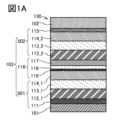


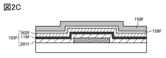

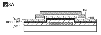

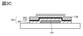


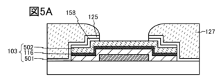


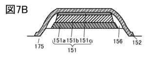


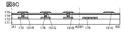


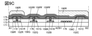


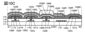
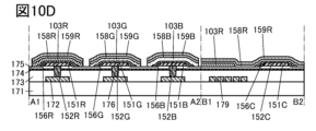


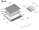

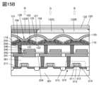


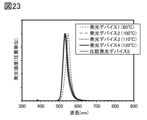
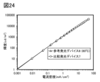


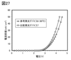
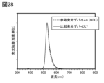


Classifications
-
- H—ELECTRICITY
- H10—SEMICONDUCTOR DEVICES; ELECTRIC SOLID-STATE DEVICES NOT OTHERWISE PROVIDED FOR
- H10K—ORGANIC ELECTRIC SOLID-STATE DEVICES
- H10K50/00—Organic light-emitting devices
- H10K50/10—OLEDs or polymer light-emitting diodes [PLED]
- H10K50/19—Tandem OLEDs
-
- H—ELECTRICITY
- H10—SEMICONDUCTOR DEVICES; ELECTRIC SOLID-STATE DEVICES NOT OTHERWISE PROVIDED FOR
- H10K—ORGANIC ELECTRIC SOLID-STATE DEVICES
- H10K71/00—Manufacture or treatment specially adapted for the organic devices covered by this subclass
- H10K71/20—Changing the shape of the active layer in the devices, e.g. patterning
-
- H—ELECTRICITY
- H10—SEMICONDUCTOR DEVICES; ELECTRIC SOLID-STATE DEVICES NOT OTHERWISE PROVIDED FOR
- H10K—ORGANIC ELECTRIC SOLID-STATE DEVICES
- H10K71/00—Manufacture or treatment specially adapted for the organic devices covered by this subclass
- H10K71/40—Thermal treatment, e.g. annealing in the presence of a solvent vapour
-
- H—ELECTRICITY
- H10—SEMICONDUCTOR DEVICES; ELECTRIC SOLID-STATE DEVICES NOT OTHERWISE PROVIDED FOR
- H10K—ORGANIC ELECTRIC SOLID-STATE DEVICES
- H10K2101/00—Properties of the organic materials covered by group H10K85/00
- H10K2101/20—Delayed fluorescence emission
Definitions
- One embodiment of the present invention relates to a method for manufacturing a light emitting device.
- one embodiment of the present invention is not limited to the above technical field.
- the technical fields of one embodiment of the present invention include light-emitting devices, semiconductor devices, display devices, display modules, light-emitting devices, power storage devices, storage devices, electronic devices, lighting devices, input devices (for example, touch sensors), and input/output devices.
- Examples include touch panels (for example, touch panels), their driving methods, or their manufacturing methods.
- display devices are expected to be applied to various uses.
- applications of large display devices include home television devices (also referred to as televisions or television receivers), digital signage (digital signage), and PID (Public Information Display).
- home television devices also referred to as televisions or television receivers
- digital signage digital signage
- PID Public Information Display
- smartphones and tablet terminals equipped with touch panels are being developed.
- VR virtual reality
- AR augmented reality
- SR substitute reality
- MR mixed reality
- a light-emitting device having a light-emitting device As a display device, for example, a light-emitting device having a light-emitting device (also referred to as a light-emitting element) has been developed.
- a light-emitting device also referred to as an EL device or EL element
- EL the phenomenon of electroluminescence
- EL is a DC constant voltage power supply that can be easily made thin and lightweight, and can respond quickly to input signals. It has characteristics such as being able to be driven using
- Patent Document 1 discloses a display device for VR using an organic EL device (also referred to as an organic EL element).
- Patent Document 2 discloses a light-emitting device with low driving voltage and good reliability, which uses a mixed film of a transition metal and an organic compound having a lone pair of electrons as an electron injection layer.
- An object of one embodiment of the present invention is to provide a method for manufacturing a light-emitting device that can be used for a display device with high display quality.
- an object of one embodiment of the present invention is to provide a method for manufacturing a light-emitting device that can be used for a high-definition display device.
- an object of one embodiment of the present invention is to provide a method for manufacturing a light-emitting device that can be used for a high-resolution display device.
- an object of one embodiment of the present invention is to provide a method for manufacturing a light-emitting device that can be used for a highly reliable display device.
- an object of one embodiment of the present invention is to provide a method for manufacturing a light-emitting device that can be used for a novel display device that is highly convenient, useful, or reliable.
- an object of one embodiment of the present invention is to provide a method for manufacturing a novel display module that is excellent in convenience, usefulness, or reliability.
- Another object of the present invention is to provide a method for manufacturing a novel electronic device that is convenient, useful, or reliable.
- Another object of the present invention is to provide a method for manufacturing a new light emitting device, a display device, a new display module, a new electronic device, or a new semiconductor device.
- One embodiment of the present invention is an organic compound that forms a first electrode and has an intermediate layer containing an alkali metal or an alkali metal compound on the first electrode between a first light-emitting layer and a second light-emitting layer.
- This is a method for manufacturing a light emitting device, in which a layer is formed, an organic compound layer is processed by a lithography method, a heat treatment is performed, and a second electrode is formed covering the first electrode and the organic compound layer.
- one embodiment of the present invention includes forming a first electrode, and having an intermediate layer containing an alkali metal or an alkali metal compound on the first electrode between the first light-emitting layer and the second light-emitting layer.
- forming an organic compound layer forming a sacrificial layer on the organic compound layer, forming a mask with a resist on the sacrificial layer, processing the organic compound layer by a lithography method, removing at least a portion of the sacrificial layer, and heating.
- This is a method for manufacturing a light emitting device in which a second electrode is formed covering the first electrode and the organic compound layer by processing.
- one embodiment of the present invention includes forming a first electrode, and having an intermediate layer containing an alkali metal or an alkali metal compound on the first electrode between the first light-emitting layer and the second light-emitting layer.
- Form an organic compound layer form a sacrificial layer on the organic compound layer, form a mask with resist on the sacrificial layer, process the organic compound layer by lithography, and form an insulating layer covering the sides of the organic compound layer.
- this method of manufacturing a light emitting device at least a portion of the sacrificial layer is removed, heat treatment is performed, and a second electrode is formed covering the first electrode and the organic compound layer.
- one embodiment of the present invention is a method for manufacturing a light-emitting device in which heat treatment is performed at 100° C. or higher in each of the above structures.
- one embodiment of the present invention is a method for manufacturing a light-emitting device, in which heat treatment is performed at 100° C. or higher and 120° C. or lower in each of the above structures.
- one embodiment of the present invention is a method for manufacturing a light-emitting device in each of the above structures, in which heat treatment is performed at a temperature of 100° C. or higher and lower than the glass transition temperature of the organic compound contained in the upper surface of the organic compound layer.
- One embodiment of the present invention can provide a method for manufacturing a light-emitting device that can be used for a display device with high display quality. Alternatively, one embodiment of the present invention can provide a method for manufacturing a light-emitting device that can be used for a high-definition display device. Alternatively, one embodiment of the present invention can provide a method for manufacturing a light-emitting device that can be used for a high-resolution display device. Alternatively, one embodiment of the present invention can provide a method for manufacturing a light-emitting device that can be used for a highly reliable display device. Alternatively, one embodiment of the present invention can provide a method for manufacturing a light-emitting device that can be used for a novel display device that is highly convenient, useful, or reliable.
- one embodiment of the present invention can provide a novel method for manufacturing a display module that is highly convenient, useful, or reliable.
- a method for manufacturing a light emitting device, a new display module, a new electronic device, or a new semiconductor device that can be used in a new display device can be provided.
- FIGS. 1A and 1B are diagrams representing light emitting devices.
- 2A to 2D are cross-sectional views showing an example of a method for manufacturing a light emitting device.
- 3A to 3D are cross-sectional views showing an example of a method for manufacturing a light emitting device.
- 4A to 4D are cross-sectional views showing an example of a method for manufacturing a light emitting device.
- 5A to 5C are cross-sectional views showing an example of a method for manufacturing a light emitting device.
- 6A and 6B are a top view and a cross-sectional view of the light emitting device.
- 7A to 7D are diagrams representing light emitting devices.
- 8A to 8E are cross-sectional views illustrating an example of a method for manufacturing a display device.
- 9A to 9D are cross-sectional views illustrating an example of a method for manufacturing a display device.
- 10A to 10D are cross-sectional views illustrating an example of a method for manufacturing a display device.
- 11A to 11C are cross-sectional views illustrating an example of a method for manufacturing a display device.
- 12A to 12C are cross-sectional views illustrating an example of a method for manufacturing a display device.
- 13A to 13C are cross-sectional views illustrating an example of a method for manufacturing a display device.
- 14A and 14B are perspective views showing an example of the configuration of a display module.
- 15A and 15B are cross-sectional views showing an example of the configuration of a display device.
- 16A to 16D are diagrams illustrating an example of an electronic device.
- 17A to 17F are diagrams illustrating an example of an electronic device.
- FIG. 18 is a diagram showing the luminance-current density characteristics of Light-emitting Device 1 and Comparative Light-emitting Device 2.
- FIG. 19 is a diagram showing the brightness-voltage characteristics of Light-emitting Device 1 and Comparative Light-emitting Device 2.
- FIG. 20 is a diagram showing current efficiency-luminance characteristics of Light-emitting Device 1 and Comparative Light-emitting Device 2.
- FIG. 21 is a diagram showing current density-voltage characteristics of Light-emitting Device 1 and Comparative Light-emitting Device 2.
- FIG. 22 is a diagram showing current efficiency-current density characteristics of Light-emitting Device 1 and Comparative Light-emitting Device 2.
- FIG. 23 is a diagram showing the emission spectra of Light Emitting Device 1 and Comparative Light Emitting Device 2.
- FIG. 24 is a diagram showing the brightness-current density characteristics of the reference light-emitting device 3 and the comparative light-emitting device 4.
- FIG. 25 is a diagram showing the brightness-voltage characteristics of the reference light-emitting device 3 and the comparison light-emitting device 4.
- FIG. 26 is a diagram showing the current efficiency-luminance characteristics of the reference light-emitting device 3 and the comparative light-emitting device 4.
- FIG. 27 is a diagram showing the current density-voltage characteristics of the reference light-emitting device 3 and the comparative light-emitting device 4.
- FIG. 28 is a diagram showing the emission spectra of the reference light-emitting device 3 and the comparison light-emitting device 4.
- FIG. 29 is a diagram showing the TDS analysis results of Sample 1.
- FIG. 30 is a diagram showing the TDS analysis results of Comparative Sample 2.
- FIG. 31 is a diagram showing the TDS analysis results of Comparative Sample 3.
- film and “layer” can be interchanged depending on the situation or circumstances.
- conductive layer can be changed to the term “conductive film.”
- insulating film can be changed to the term “insulating layer.”
- a device manufactured using a metal mask or an FMM fine metal mask, high-definition metal mask
- a device with an MM (metal mask) structure is sometimes referred to as a device with an MML (metal maskless) structure.
- holes or electrons may be referred to as “carriers.”
- a hole injection layer or an electron injection layer is called a “carrier injection layer”
- a hole transport layer or an electron transport layer is called a “carrier transport layer”
- a hole blocking layer or an electron blocking layer is called a “carrier injection layer.”
- the carrier injection layer, carrier transport layer, and carrier block layer described above may not be clearly distinguishable depending on their respective cross-sectional shapes or characteristics.
- one layer may serve as two or three functions among a carrier injection layer, a carrier transport layer, and a carrier block layer.
- a light emitting device (also referred to as a light emitting element) has an EL layer between a pair of electrodes.
- the EL layer has at least a light emitting layer.
- a light-receiving device (also referred to as a light-receiving element) has an active layer that functions as at least a photoelectric conversion layer between a pair of electrodes.
- one of a pair of electrodes is sometimes referred to as a pixel electrode, and the other is sometimes referred to as a common electrode.
- tapeered shape refers to a shape in which at least a portion of the side surface of the structure is inclined with respect to the substrate surface. For example, it is preferable to have a region where the angle between the inclined side surface and the substrate surface (also referred to as a taper angle) is less than 90°.
- the side surface of the structure and the substrate surface do not necessarily have to be completely flat, and may be substantially planar with a minute curvature, or may be substantially planar with minute irregularities.
- Embodiment 1 As one method for manufacturing an organic semiconductor film into a predetermined shape, a vacuum evaporation method using a metal mask (mask evaporation) is widely used. However, as the density and definition of mask deposition continues to increase, mask deposition is approaching its limit due to various reasons such as alignment accuracy and spacing between substrates. . On the other hand, by processing the shape of an organic semiconductor film using a lithography method, a more precise pattern can be formed. Furthermore, since this method can be easily applied to a large area, research on processing organic semiconductor films using lithography is also progressing.
- An organic EL element has an organic compound layer (corresponding to the above-mentioned organic semiconductor film) containing a luminescent substance between the electrodes (between the first electrode and the second electrode), and the organic compound layer is formed from the electrode to the organic compound layer. It has a configuration in which light is emitted by energy generated by recombining carriers (holes and electrons) in the injection layer.
- an alkali metal such as lithium (Li) or a compound of the alkali metal is used for the electron injection layer in contact with the cathode, thereby realizing a low voltage.
- One way to solve this problem is to perform a lithography process during the formation of the organic compound layer of the light emitting device (before forming the layer containing the alkali metal or alkali metal compound). That is, in this method, lithography is performed to process the organic compound layer before forming the electron injection layer, and then the electron injection layer and subsequent steps are performed to avoid deterioration of the characteristics.
- tandem light emitting device has an organic semiconductor layer with a structure in which multiple light emitting layers are stacked in series with an intermediate layer in between, and the intermediate layer has a structure in which electrons are transferred to the light emitting layer on the anode side.
- a layer containing an alkali metal or an alkali metal compound is included for implantation. Since the intermediate layer exists between the light emitting layers, if the light emitting layer is to be processed by lithography, the intermediate layer will necessarily be exposed to the lithography process.
- the drive voltage of the light emitting device increases significantly and the current This resulted in a significant drop in efficiency.
- a layer containing an alkali metal or an alkali metal compound has the property of easily adsorbing water in the atmosphere, and this causes a significant increase in the driving voltage of a light emitting device and a decrease in current efficiency when the layer is exposed to a lithography process. Furthermore, by performing a step to sufficiently remove water from the layer, a tandem light-emitting device with good characteristics can be produced even when the layer is exposed to a lithography process. The present inventors have discovered that it is possible.
- heat treatment is performed after the step of processing an organic compound layer containing an alkali metal or an alkali metal compound using a lithography method.
- a light emitting device By producing a light emitting device using such a method, water can be sufficiently removed from the organic compound layer containing an alkali metal or an alkali metal compound. Therefore, it is possible to suppress a significant increase in drive voltage of the light emitting device and prevent a decrease in current efficiency. As a result, a light emitting device with good characteristics can be obtained. Further, it is possible to provide a high-definition display that can withstand use in VR, AR, etc., and a display device with good characteristics can be provided.
- FIG. 1A shows a light-emitting device 130 that is an example of a light-emitting device that can be manufactured by the method for manufacturing a light-emitting device of one embodiment of the present invention.
- the light emitting device 130 is a tandem light emitting device having an organic compound layer 103 including a plurality of light emitting units between a first electrode 101 including an anode and a second electrode 102 including a cathode.
- the light emitting device 130 includes, as the organic compound layer 103, a first light emitting unit 501 including a first light emitting layer 113_1, a second light emitting unit 502 including a second light emitting layer 113_2, and an intermediate layer 116. .
- a method for manufacturing a light-emitting device of one embodiment of the present invention will be described using as an example a light-emitting device having one intermediate layer 116 as the organic compound layer 103 and two light-emitting units; According to the method for manufacturing a light-emitting device of one embodiment, a light-emitting device having an intermediate layer (also referred to as a charge generation layer) of n (n is an integer of 1 or more) layers and n+1 layers of light-emitting units as the organic compound layer 103 is manufactured. You can also. For example, in the light emitting device 130 shown in FIG.
- the organic compound layer 103 includes a first light emitting unit 501, a first intermediate layer 116_1, a second light emitting unit 502, and a second intermediate layer.
- 116_2 and a third light emitting unit 503 is an example of a tandem light emitting device. Note that the color gamut of light exhibited by the light emitting layer in each light emitting unit may be the same or different. Furthermore, the light-emitting layer may have a single layer or a laminated structure.
- a configuration in which the first light emitting unit and the third light emitting unit emit light in the blue region, and the second light emitting unit emits light in the red region and light in the green region from the light emitting layer of the laminated structure allows white light to be emitted. Obtainable.
- the light-emitting device 130 is a light-emitting device manufactured by the method for manufacturing a light-emitting device of one embodiment of the present invention using a lithography method, and of the organic compound layer 103, at least the second light-emitting layer 113_2 and the second light-emitting layer Since the layers closer to the first electrode 101 than the layer 113_2 are processed at the same time, their ends are approximately aligned in the vertical direction.
- the intermediate layer 116 is a layer containing at least an alkali metal or an alkali metal compound. More specifically, the intermediate layer 116 is a layer that includes an N-type layer 119 and a P-type layer 117, and it is preferable that the N-type layer 119 includes an alkali metal or an alkali metal compound. Specific examples of alkali metals include lithium, sodium, potassium, rubidium, cesium, francium, and the like. Specific examples of the alkali metal compound include the aforementioned alkali metal compounds, such as lithium compounds such as lithium oxide. In addition to the alkali metal or alkali metal compound, the N-type layer 119 may include an organic compound having electron transporting properties.
- the P-type layer 117 is located closer to the second electrode 102 than the N-type layer 119 is. Further, an electronic relay layer 118 may be provided between the N-type layer 119 and the P-type layer 117 to smoothly transfer electrons between these two layers.
- the first light emitting unit 501 and the second light emitting unit 502 may include other functional layers in addition to the light emitting layer.
- the first light emitting unit 501 is provided with a hole injection layer 111, a first hole transport layer 112_1, and a first electron transport layer 114_1 in addition to the first light emitting layer 113_1,
- the second light emitting unit 502 is illustrated as having a second hole transport layer 112_2, a second electron transport layer 114_2, and an electron injection layer 115 in addition to the second light emitting layer 113_2.
- the structure of the organic compound layer 103 in the present invention is not limited to this, and one of the layers may not be provided, or another layer may be provided. Note that other layers typically include a carrier block layer, an exciton block layer, and the like.
- the intermediate layer 116 includes the N-type layer 119
- the N-type layer 119 plays the role of an electron injection layer in the light emitting unit on the anode side. Therefore, the light emitting unit on the anode side (the first light emitting unit 501 in FIG. 1A) may or may not have an electron injection layer.
- the intermediate layer 116 includes the P-type layer 117
- the P-type layer 117 plays the role of a hole injection layer in the light emitting unit on the cathode side. Therefore, the light emitting unit on the cathode side (second light emitting unit 502 in FIG. 1A) may or may not have a hole injection layer.
- a first electrode 101 is formed on a substrate 105.
- the first electrode 101 can be formed using, for example, a photolithography method. Specifically, after a resist mask is formed on a conductive film formed on the substrate 105, a part of the conductive film is removed by an etching method. A portion of the conductive film can be removed, for example, by wet etching. Note that a part of the conductive film may be removed by dry etching.
- an organic compound film 103f that will later become the organic compound layer 103 is formed on the substrate 105 and the first electrode 101.
- the organic compound film 501f is a film that will later become the first light emitting unit 501
- the intermediate film 116f is a film that will later become the intermediate layer 116
- the organic compound film 502f is a film that will later become the second light emitting unit 502. It is a membrane that becomes
- the intermediate film 116f included in the organic compound film 103f is a film containing at least an alkali metal or an alkali metal compound. More specifically, the intermediate film 116f is a film having an N-type film and a P-type film, and it is preferable that the N-type film contains an alkali metal or an alkali metal compound. Specific examples of alkali metals include lithium, sodium, potassium, rubidium, cesium, francium, and the like. Specific examples of the alkali metal compound include the aforementioned alkali metal compounds, such as lithium compounds such as lithium oxide. Note that the N-type film may contain, in addition to the alkali metal or alkali metal compound, an organic compound having electron transporting properties.
- the organic compound film 103f can be formed by, for example, a vapor deposition method, specifically, a vacuum vapor deposition method. Further, the organic compound film 103f may be formed by a transfer method, a printing method, an inkjet method, a coating method, or the like.
- a sacrificial film 158f that will later become the sacrificial layer 158 and a mask film 159f that will later become the mask layer 159 are sequentially formed on the organic compound film 103f.
- the method for forming the sacrificial film 158f and the mask film 159f reference can be made to the method for forming the sacrificial film 158Rf and the mask film 159Rf, which will be described in detail in later embodiments.
- a resist mask 190 is formed on the mask film 159f at a position overlapping with the first electrode 101.
- the resist mask 190 can be formed by applying a photosensitive material (photoresist), exposing it to light, and developing it. Note that the resist mask 190 may be manufactured using either a positive resist material or a negative resist material.
- a portion of the mask film 159f is removed to form a mask layer 159.
- resist mask 190 is removed.
- the mask layer 159 as a mask also referred to as a hard mask
- a portion of the sacrificial film 158f is removed to form a sacrificial layer 158 (see FIG. 3A).
- the organic compound film 103f (organic compound film 501f, intermediate film 116f, and organic compound film 502f) is processed to form the organic compound layer 103 (first light emitting unit 501, intermediate layer 116). , and a second light emitting unit 502).
- the organic compound layer 103 is formed by removing a portion of the organic compound film 103f using the mask layer 159 and the sacrificial layer 158 as hard masks.
- a specific method for processing the organic compound film 103f reference can be made to a method for processing the organic compound film 103Rf, which will be described in detail in a later embodiment.
- the mask layer 159 is formed by forming the resist mask 190 over the mask film 159f and using the resist mask 190 to remove a portion of the mask film 159f. Thereafter, the organic compound layer 103 is formed by removing a portion of the organic compound film 103f using the mask layer 159 as a hard mask. Therefore, it can be said that the organic compound layer 103 is formed by processing the organic compound film 103f using a lithography method. Further, the organic compound film 103f includes an intermediate film 116f, and the intermediate film 116f is a film containing at least an alkali metal or an alkali metal compound.
- the organic compound layer 103 containing an alkali metal or an alkali metal compound is formed by processing the organic compound film 103f containing an alkali metal or an alkali metal compound using a lithography method. Note that a portion of the organic compound film 103f may be removed using the resist mask 190. Thereafter, resist mask 190 may be removed.
- mask layer 159 is preferably removed.
- a method similar to the process of processing the mask film 159f can be used. Details of the method for removing the mask layer 159 will be explained in detail in a later embodiment.
- Heat treatment may be performed after removing the mask layer.
- heat treatment can be performed under an inert gas atmosphere or a reduced pressure atmosphere.
- the heat treatment can be performed at a substrate temperature of 50°C or more and 200°C or less, preferably 60°C or more and 150°C or less, and more preferably 70°C or more and 120°C or less.
- a reduced pressure atmosphere is preferable because drying can be performed at a lower temperature.
- an inorganic insulating film 125f that will later become the inorganic insulating layer 125 is formed so as to cover the organic compound layer 103 and the sacrificial layer 158.
- a specific method for forming the inorganic insulating film 125f will be described in detail in a later embodiment.
- an insulating film 127f that will later become the insulating layer 127 is formed on the inorganic insulating film 125f.
- the insulating film 127f is preferably formed using a photosensitive material by spin coating, for example, and more specifically, it is preferably formed using a photosensitive resin composition containing an acrylic resin. A specific method for forming the insulating film 127f will be described in detail in a later embodiment.
- the insulating film 127f is exposed to visible light or ultraviolet light.
- a positive photosensitive resin composition containing an acrylic resin for the insulating film 127f visible light or ultraviolet rays are applied to the first electrode 101, which is the area where the insulating layer 127 will not be formed in a later step. irradiate.
- a negative photosensitive material is used for the insulating film 127f, the region where the insulating layer 127 is formed is irradiated with visible light or ultraviolet rays.
- a specific method of exposing the insulating film 127f will be described in detail in a later embodiment.
- FIG. 4B development is performed to remove a portion of the insulating film 127f and form an insulating layer 127a.
- the insulating layer 127a is formed in a region that does not overlap with the first electrode 101. A specific method for forming the insulating layer 127a will be described in detail in a later embodiment.
- etching is performed using the insulating layer 127a as a mask to remove a portion of the inorganic insulating film 125f and reduce the thickness of a portion of the sacrificial layer 158.
- an inorganic insulating layer 125 is formed under the insulating layer 127a.
- the surface of the thinner portion of the sacrificial layer 158 is exposed.
- the insulating layer 127a can be transformed into a shape having a tapered side surface, thereby forming the insulating layer 127 (FIG. 4D).
- the heat treatment is performed at a temperature lower than the allowable temperature limit of the organic compound layer.
- the heat treatment can be performed at a substrate temperature of 50° C. or higher and 200° C. or lower, preferably 60° C. or higher and 150° C. or lower, and more preferably 70° C. or higher and 130° C. or lower.
- the heating atmosphere may be an air atmosphere or an inert gas atmosphere. Further, the heating atmosphere may be an atmospheric pressure atmosphere or a reduced pressure atmosphere. Details of the heat treatment after the etching treatment using the insulating layer 127a as a mask will be described in detail in a later embodiment.
- etching is performed using the insulating layer 127 as a mask to remove a portion of the sacrificial layer 158 (which can also be called a thin portion of the sacrificial layer 158). Note that a portion of the inorganic insulating layer 125 may also be removed. As a result, an opening is formed in the sacrificial layer 158, and a part of the upper surface of the organic compound layer 103 is exposed.
- Removal of a portion of the sacrificial layer 158 by etching using the insulating layer 127 as a mask is performed by wet etching.
- wet etching method damage to the organic compound layer 103 can be reduced compared to when using the dry etching method.
- a specific method for removing a portion of the sacrificial layer 158 by etching using the insulating layer 127 as a mask will be described in detail in a later embodiment.
- heat treatment is further performed.
- the heat treatment can remove water contained in the organic compound layer 103, water adsorbed on the surface of the organic compound layer 103, water contained in the intermediate layer 116, which is a layer containing an alkali metal or an alkali metal compound, and the like.
- the shape of the insulating layer 127 may change due to the heat treatment. Specifically, the insulating layer 127 may spread to cover at least one of the ends of the inorganic insulating layer 125, the ends of the sacrificial layer 158, and the top surface of the organic compound layer 103.
- the heat treatment is preferably performed at a temperature higher than the temperature at which water desorbs from the organic compound layer 103 and lower than the glass transition temperature of the organic compound contained in the organic compound layer 103. A temperature lower than the glass transition temperature of is preferred.
- the substrate temperature is preferably 80°C or more and 130°C or less, preferably 90°C or more and 120°C or less, more preferably 100°C or more and 120°C or less, and even more preferably 100°C or more and 110°C or less.
- the heating atmosphere may be an air atmosphere or an inert gas atmosphere. Further, the heating atmosphere may be an atmospheric pressure atmosphere or a reduced pressure atmosphere, but a reduced pressure atmosphere is preferable in order to prevent the water desorbed from the organic compound layer 103 from being re-adsorbed.
- the second electrode 102 is formed on the organic compound layer 103 and the insulating layer 127.
- the second electrode 102 can be formed by a method such as a sputtering method or a vacuum evaporation method.
- the second electrode 102 may be formed by stacking a film formed by a vapor deposition method and a film formed by a sputtering method.
- the light emitting device 130 can be manufactured.
- an organic compound layer 502b and a second electrode 102 can be formed on the organic compound layer 103. Since the organic compound layer 502b is formed after the lithography process, a material that does not have high heat resistance can be selected as a material that can be used for the organic compound layer 502b, which widens the range of material selection.
- a material that functions as an electron injection layer in the light emitting device 130 can be used, for example.
- a layer containing an alkali metal or an alkali metal compound can be formed as the organic compound layer 502b.
- a layer containing an alkali metal or an alkali metal compound By forming a layer containing an alkali metal or an alkali metal compound after the lithography process, it is possible to prevent a significant increase in driving voltage or a significant decrease in current efficiency of the light emitting device. Note that when the organic compound layer 502b is provided, the stacked structure of the organic compound layer 103 and the organic compound layer 502b corresponds to the organic compound layer 103 in the first embodiment.
- the island-shaped organic compound layer 103 is not formed using a fine metal mask, but is processed after forming a film over one surface. Since it is formed by this process, it is possible to form an island-like layer with a uniform thickness. Then, a light-emitting device that realizes a high-definition display device or a display device with a high aperture ratio can be manufactured. Furthermore, even a tandem-type light-emitting device manufactured using a lithography method can provide a light-emitting device with good characteristics.
- This embodiment mode can be combined with other embodiment modes or examples as appropriate. Further, in this specification, when a plurality of configuration examples are shown in one embodiment, the configuration examples can be combined as appropriate.
- Embodiment 2 In this embodiment, materials that can be used for each layer of the light emitting device 130 described in Embodiment 1 will be described.
- the intermediate film 116f is a film containing at least an alkali metal or an alkali metal compound. More specifically, the intermediate film 116f is a film having an N-type film and a P-type film, and it is preferable that the N-type film contains an alkali metal or an alkali metal compound. Specific examples of alkali metals include lithium, sodium, potassium, rubidium, cesium, francium, and the like. Specific examples of the alkali metal compound include the aforementioned alkali metal compounds, such as lithium compounds such as lithium oxide. Note that the N-type film may contain, in addition to the alkali metal or alkali metal compound, an organic compound having electron transporting properties.
- lithium or a lithium compound as the alkali metal or alkali metal compound
- specific examples include lithium, lithium complexes, lithium compounds, and lithium alloys.
- alkyls such as lithium, lithium oxide, lithium nitride, lithium carbonate, lithium fluoride, 8-quinolinolato-lithium (abbreviation: Liq), 2-methyl-8-quinolinolato-lithium (abbreviation: Li-mq), etc.
- Examples include lithium complexes containing groups.
- the organic compound having an electron transporting property that can be used for the N-type layer 119 has an electron mobility of 1 ⁇ 10 ⁇ 7 cm 2 /Vs or more, preferably 1
- a substance having an electron mobility of ⁇ 10 ⁇ 6 cm 2 /Vs or more is preferable. Note that materials other than these can be used as long as they have a higher transportability for electrons than for holes.
- the above organic compound is preferably an organic compound having a ⁇ -electron deficient heteroaromatic ring.
- organic compounds having a ⁇ electron-deficient heteroaromatic ring include organic compounds containing a heteroaromatic ring having a polyazole skeleton, organic compounds containing a heteroaromatic ring having a pyridine skeleton, and organic compounds containing a heteroaromatic ring having a diazine skeleton. and an organic compound containing a heteroaromatic ring having a triazine skeleton.
- organic compound having an electron transport property that can be used for the N-type layer 119
- 2-(4-biphenylyl)-5-(4-tert-butylphenyl)-1,3,4- Oxadiazole (abbreviation: PBD)
- 3-(4-biphenylyl)-4-phenyl-5-(4-tert-butylphenyl)-1,2,4-triazole (abbreviation: TAZ)
- 1,3-bis [5-(p-tert-butylphenyl)-1,3,4-oxadiazol-2-yl]benzene abbreviation: OXD-7
- 9-[4-(5-phenyl-1,3,4) -oxadiazol-2-yl)phenyl]-9H-carbazole (abbreviation: CO11), 2,2',2''-(1,3,5-benzenetriyl)tris(1-phenyl-1H-benzo imidazole) (abbreviation
- organic compounds having a phenanthroline skeleton such as Bphen, BCP, NBphen and mPPhen2P are preferred, and organic compounds having a phenanthroline dimer structure such as mPPhen2P have excellent stability and are more preferred.
- the P-type layer 117 which is a charge generation layer, is preferably formed of a composite material containing a material having acceptor properties and an organic compound having hole transport properties.
- Various organic compounds can be used as organic compounds with hole transport properties for use in composite materials, such as aromatic amine compounds, heteroaromatic compounds, aromatic hydrocarbons, and polymer compounds (oligomers, dendrimers, polymers, etc.). I can do it.
- the organic compound having hole transport properties used in the composite material is preferably an organic compound having a hole mobility of 1 ⁇ 10 ⁇ 6 cm 2 /Vs or more.
- the organic compound having hole transport properties used in the composite material is preferably a compound having a condensed aromatic hydrocarbon ring or a ⁇ -electron-excessive heteroaromatic ring.
- Preferred examples of the fused aromatic hydrocarbon ring include an anthracene ring and a naphthalene ring.
- a fused aromatic ring containing at least one of a pyrrole skeleton, a furan skeleton, and a thiophene skeleton is preferable, and specifically, a carbazole ring, a dibenzothiophene ring, or an aromatic A ring or a ring fused with a heteroaromatic ring is preferred.
- the organic compound having such hole-transporting properties preferably has one of a carbazole skeleton, a dibenzofuran skeleton, a dibenzothiophene skeleton, and an anthracene skeleton.
- a carbazole skeleton a dibenzofuran skeleton, a dibenzothiophene skeleton, and an anthracene skeleton.
- an aromatic amine having a substituent containing a dibenzofuran ring or a dibenzothiophene ring an aromatic monoamine having a naphthalene ring, or an aromatic monoamine in which a 9-fluorenyl group is bonded to the nitrogen of the amine via an arylene group.
- the organic compound having hole-transporting properties is a substance having an N,N-bis(4-biphenyl)amino group because a light-emitting device with a good lifetime can be produced.
- the organic compound having hole transport properties as described above includes N-(4-biphenyl)-6,N-diphenylbenzo[b]naphtho[1,2-d]furan-8-amine.
- BnfABP N,N-bis(4-biphenyl)-6-phenylbenzo[b]naphtho[1,2-d]furan-8-amine
- BBABnf 4,4'-bis( 6-phenylbenzo[b]naphtho[1,2-d]furan-8-yl)-4''-phenyltriphenylamine
- BnfBB1BP N,N-bis(4-biphenyl)benzo[b] Naphtho[1,2-d]furan-6-amine
- BBABnf(6) N,N-bis(4-biphenyl)benzo[b]naphtho[1,2-d]furan-6-amine
- aromatic amine compounds include N,N'-di(p-tolyl)-N,N'-diphenyl-p-phenylenediamine (abbreviation: DTDPPA), 4, 4'-bis[N-(4-diphenylaminophenyl)-N-phenylamino]biphenyl (abbreviation: DPAB), 4,4'-bis(N- ⁇ 4-[N'-(3-methylphenyl)- N'-phenylamino]phenyl ⁇ -N-phenylamino)biphenyl (abbreviation: DNTPD), 1,3,5-tris[N-(4-diphenylaminophenyl)-N-phenylamino]benzene (abbreviation: DPA3B) etc. can also be used.
- DTDPPA 4, 4'-bis[N-(4-diphenylaminophenyl)-N-phenylamino]biphenyl
- DPAB 4,
- an organic compound having an electron-withdrawing group (halogen group, cyano group, etc.) can be used, and 7,7,8,8-tetracyano-2, 3,5,6-tetrafluoroquinodimethane (abbreviation: F4-TCNQ), chloranil, 2,3,6,7,10,11-hexacyano-1,4,5,8,9,12-hexaazatriphenylene (abbreviation: HAT-CN), 1,3,4,5,7,8-hexafluorotetracyano-naphthoquinodimethane (abbreviation: F6-TCNNQ), 2-(7-dicyanomethylene-1,3,4 , 5,6,8,9,10-octafluoro-7H-pyrene-2-ylidene)malononitrile, and the like.
- F4-TCNQ 7,7,8,8-tetracyano-2, 3,5,6-tetrafluoroquinodimethane
- HAT-CN 2,3,
- a compound such as HAT-CN in which an electron-withdrawing group is bonded to a condensed aromatic ring having a plurality of heteroatoms is thermally stable and is therefore preferable.
- [3] radialene derivatives having electron-withdrawing groups are preferable because they have very high electron-accepting properties, and specifically, ⁇ , ⁇ ', ⁇ '' -1,2,3-cyclopropane triylidene triylidene [4-cyano-2,3,5,6-tetrafluorobenzeneacetonitrile], ⁇ , ⁇ ', ⁇ ''-1,2,3-cyclopropane triylidene Tris [2,6-dichloro-3,5-difluoro-4-(trifluoromethyl)benzeneacetonitrile], ⁇ , ⁇ ', ⁇ ''-1,2,3-cyclopropane triyliden
- the electron relay layer 118 contains a substance having an electron transport property, and has a function of preventing interaction between the N-type layer 119 and the P-type layer 117 and smoothly transferring electrons.
- the LUMO (Lowest Unoccupied Molecular Orbital) level of the substance having electron transport properties included in the electron relay layer 118 is the same as the LUMO level of the acceptor substance in the P-type layer 117 and the first electrode 101 side.
- the LUMO level is preferably between the LUMO level of the organic compound contained in the layer in contact with the intermediate layer 116 in the light emitting unit (the first electron transport layer 114_1 in the first light emitting unit 501 in FIG. 1A).
- the specific energy level of the LUMO level in the material having electron transport properties used in the electron relay layer 118 is preferably ⁇ 5.0 eV or more, preferably ⁇ 5.0 eV or more and ⁇ 3.0 eV or less. Note that as the substance having electron transport properties used in the electron relay layer 118, it is preferable to use a phthalocyanine-based material or a metal complex having a metal-oxygen bond and an aromatic ligand.
- the first electrode 101 is an electrode including an anode.
- the first electrode 101 may have a laminated structure, in which case the layer in contact with the organic compound layer 103 functions as an anode.
- the anode is preferably formed using a metal, an alloy, a conductive compound, a mixture thereof, or the like having a large work function (specifically, 4.0 eV or more).
- a metal, an alloy, a conductive compound, a mixture thereof, or the like having a large work function (specifically, 4.0 eV or more).
- ITO indium oxide-tin oxide
- IWZO indium oxide-zinc oxide
- These conductive metal oxide films are usually formed by a sputtering method, but they may also be formed by applying a sol-gel method or the like.
- indium oxide-zinc oxide is formed by a sputtering method using a target in which 1 to 20 wt % of zinc oxide is added to indium oxide.
- indium oxide (IWZO) containing tungsten oxide and zinc oxide is formed by a sputtering method using a target containing 0.5 to 5 wt% of tungsten oxide and 0.1 to 1 wt% of zinc oxide relative to indium oxide. You can also.
- materials used for the anode include, for example, gold (Au), platinum (Pt), nickel (Ni), tungsten (W), chromium (Cr), molybdenum (Mo), iron (Fe), cobalt ( Co), copper (Cu), palladium (Pd), or a nitride of a metal material (eg, titanium nitride).
- a metal material eg, titanium nitride
- graphene can also be used as a material for the anode. Note that by using the composite material constituting the P-type layer 117 in the intermediate layer 116 as a layer in contact with the anode (typically a hole injection layer), the electrode material can be selected regardless of the work function. It becomes like this.
- the organic compound layer 103 has a layered structure.
- the laminated structure includes a first light emitting unit 501 including a first light emitting layer 113_1, a second light emitting unit 502 including an intermediate layer 116, and a second light emitting layer 113_2.
- a configuration in which two light emitting units are stacked with an intermediate layer in between is shown here, a configuration in which three or more light emitting units are stacked may also be used. Also in this case, an intermediate layer is provided between the light emitting units.
- each light emitting unit also has a laminated structure.
- the light emitting unit is not limited to the configuration shown in FIG. 1A, but may include a hole injection layer, a hole transport layer, an electron transport layer, an electron injection layer, a carrier block layer (hole block layer, electron block layer), an exciton block layer, etc. , can be configured using various functional layers as appropriate.
- the hole injection layer 111 is provided in contact with the anode, and has a function of facilitating injection of holes into the organic compound layer 103 (first light emitting unit 501).
- the hole injection layer 111 is made of a phthalocyanine compound such as phthalocyanine (abbreviation: H2Pc ), a phthalocyanine complex compound such as copper phthalocyanine (abbreviation: CuPc), 4,4'-bis[N-(4-diphenyl) aminophenyl)-N-phenylamino]biphenyl (abbreviation: DPAB), 4,4'-bis(N- ⁇ 4-[N'-(3-methylphenyl)-N'-phenylamino]phenyl ⁇ -N- Formed from aromatic amine compounds such as phenylamino)biphenyl (abbreviation: DNTPD), or polymers such as poly(3,4-ethylenedioxythiophene)/(polystyrene sul
- the hole injection layer 111 may be formed of a substance that has electron acceptor properties.
- the substances listed as the acceptor properties used in the composite material constituting the P-type layer 117 in the intermediate layer 116 can be similarly used.
- the hole injection layer 111 may be formed using the same composite material as the P-type layer 117 in the intermediate layer 116.
- the organic compound having hole transport properties used in the composite material has a HOMO (Highest Occupied Molecular Orbital) level of -5.7 eV or more -5.4 eV. More preferably, the material has the following relatively deep HOMO level.
- An organic compound having a hole transporting property used in a composite material has a relatively deep HOMO level, so that holes can be easily injected into a hole transporting layer, and a light emitting device with a good lifetime can be obtained. becomes easier.
- the organic compound with hole transport properties used in the composite material has a relatively deep HOMO level, the induction of holes can be moderately suppressed, and a light-emitting device with a good lifetime can be obtained. can.
- hole injection layer 111 By forming the hole injection layer 111, hole injection properties are improved, and a light emitting device with low driving voltage can be obtained.
- organic compounds that have acceptor properties are easy to vapor deposit and form a film, so they are materials that are easy to use.
- the second light emitting unit 502 is not provided with a hole injection layer, but the second light emitting unit is provided with a hole injection layer. It may be provided.
- the hole transport layer (first hole transport layer 112_1, second hole transport layer 112_2) is formed containing an organic compound having hole transport properties.
- the organic compound having hole transport properties preferably has a hole mobility of 1 ⁇ 10 ⁇ 6 cm 2 /Vs or more.
- the above-mentioned materials having hole transport properties include 4,4'-bis[N-(1-naphthyl)-N-phenylamino]biphenyl (abbreviation: NPB), N,N'-diphenyl-N,N'- Bis(3-methylphenyl)-4,4'-diaminobiphenyl (abbreviation: TPD), N,N'-bis(9,9'-spirobi[9H-fluoren]-2-yl)-N,N'- Diphenyl-4,4'-diaminobiphenyl (abbreviation: BSPB), 4-phenyl-4'-(9-phenylfluoren-9-yl)triphenylamine (abbreviation: BPAFLP), 4-phenyl-3'-(9 -Phenylfluoren-9-yl)triphenylamine (abbreviation: mBPAFLP), 4-phenyl-4'-(9-phenyl-9H
- compounds having an aromatic amine skeleton and compounds having a carbazole skeleton are preferable because they have good reliability, high hole transportability, and contribute to reduction in driving voltage.
- the substances listed as materials having hole transport properties used in the composite material of the hole injection layer 111 can also be suitably used as materials constituting the hole transport layer.
- the light-emitting layers (first light-emitting layer 113_1, second light-emitting layer 113_2) preferably contain a light-emitting substance and a host material. Note that the light-emitting layer may contain other materials at the same time. Alternatively, it may be a laminate of two layers having different compositions.
- the luminescent substance may be a fluorescent luminescent substance, a phosphorescent luminescent substance, a substance exhibiting thermally activated delayed fluorescence (TADF), or any other luminescent substance.
- TADF thermally activated delayed fluorescence
- Examples of materials that can be used as fluorescent substances in the light-emitting layer include the following. Further, fluorescent substances other than these can also be used.
- fused aromatic diamine compounds typified by pyrene diamine compounds such as 1,6FLPAPrn, 1,6mMemFLPAPrn, and 1,6BnfAPrn-03 are preferred because they have high hole-trapping properties and are excellent in luminous efficiency or reliability.
- a phosphorescent substance When a phosphorescent substance is used as a luminescent substance in the luminescent layer, examples of materials that can be used include the following.
- Organometallic iridium complex having an imidazole skeleton bis[2-(4',6'-difluorophenyl)pyridinato-N,C 2' ]iridium(III) tetrakis(1-pyrazolyl)borate (abbreviation: FIr6), bis[ 2-(4',6'-difluorophenyl)pyridinato-N, C2' ]iridium(III)picolinate (abbreviation: FIrpic), bis ⁇ 2-[3',5'-bis(trifluoromethyl)phenyl] Pyridinato-N,C2 ' ⁇ iridium(III)picolinate (abbreviation: [Ir( CF3ppy ) 2 (pic)]), bis[2-(4',6'-difluorophenyl)pyridinato-N, C2 ]
- Examples include organometallic iridium complexes having a pheny
- tris(4-methyl-6-phenylpyrimidinato)iridium(III) (abbreviation: [Ir(mppm) 3 ]), tris(4-t-butyl-6-phenylpyrimidinato)iridium(III) (Abbreviation: [Ir(tBuppm) 3 ]), (acetylacetonato)bis(6-methyl-4-phenylpyrimidinato)iridium(III) (abbreviation: [Ir(mppm) 2 (acac)]), ( acetylacetonato)bis(6-tert-butyl-4-phenylpyrimidinato)iridium(III) (abbreviation: [Ir(tBuppm) 2 (acac)]), (acetylacetonato)bis[6-(2- norbornyl)-4-phenylpyrimidinato]iridium(III) (abbreviation: [Ir(nbppm)
- rare earth metal complexes such as tris(acetylacetonato)(monophenanthroline)terbium(III) (abbreviation: [Tb(acac) 3 (Phen)]). These are compounds that mainly emit green phosphorescence, and have an emission peak in the wavelength range from 500 nm to 600 nm. Note that an organometallic iridium complex having a pyrimidine skeleton is particularly preferable because it has outstanding reliability and luminous efficiency.
- an organometallic iridium complex having a pyrazine skeleton can emit red light with good chromaticity.
- known phosphorescent compounds may be selected and used.
- TADF material fullerene and its derivatives, acridine and its derivatives, eosin derivatives, etc. can be used.
- Other metal-containing porphyrins include magnesium (Mg), zinc (Zn), cadmium (Cd), tin (Sn), platinum (Pt), indium (In), palladium (Pd), and the like.
- the metal-containing porphyrin include protoporphyrin-tin fluoride complex (SnF 2 (Proto IX)), mesoporphyrin-tin fluoride complex (SnF 2 (Meso IX)), and hematoporphyrin shown in the following structural formula.
- Tin fluoride complex SnF 2 (Hemato IX)
- coproporphyrin tetramethyl ester-tin fluoride complex SnF 2 (Copro III-4Me)
- octaethylporphyrin-tin fluoride complex SnF 2 (OEP)
- ethioporphyrin-tin fluoride complex SnF2 (Etio I)
- octaethylporphyrin-platinum chloride complex PtCl2OEP
- Heterocyclic compounds having one or both of these can also be used. Since the heterocyclic compound has a ⁇ -electron-rich heteroaromatic ring and a ⁇ -electron-deficient heteroaromatic ring, it has high electron-transporting properties and hole-transporting properties, and is therefore preferable.
- the skeletons having a ⁇ -electron-deficient heteroaromatic ring pyridine skeletons, diazine skeletons (pyrimidine skeletons, pyrazine skeletons, pyridazine skeletons), and triazine skeletons are preferred because they are stable and have good reliability.
- a benzofuropyrimidine skeleton, a benzothienopyrimidine skeleton, a benzofuropyrazine skeleton, and a benzothienopyrazine skeleton are preferred because they have high acceptability and good reliability.
- the skeletons having a ⁇ -electron-rich heteroaromatic ring at least one of the acridine skeleton, phenoxazine skeleton, phenothiazine skeleton, furan skeleton, thiophene skeleton, and pyrrole skeleton is stable and reliable. It is preferable to have.
- the furan skeleton is preferably a dibenzofuran skeleton
- the thiophene skeleton is preferably a dibenzothiophene skeleton.
- the pyrrole skeleton an indole skeleton, a carbazole skeleton, an indolocarbazole skeleton, a bicarbazole skeleton, and a 3-(9-phenyl-9H-carbazol-3-yl)-9H-carbazole skeleton are particularly preferable.
- a substance in which a ⁇ -electron-rich heteroaromatic ring and a ⁇ -electron-deficient heteroaromatic ring are directly bonded has both the electron-donating property of the ⁇ -electron-rich heteroaromatic ring and the electron-accepting property of the ⁇ -electron-deficient heteroaromatic ring. This is particularly preferable because thermally activated delayed fluorescence can be efficiently obtained because the energy difference between the S1 level and the T1 level becomes small.
- an aromatic ring to which an electron-withdrawing group such as a cyano group is bonded may be used instead of the ⁇ electron-deficient heteroaromatic ring.
- an aromatic amine skeleton, a phenazine skeleton, etc. can be used.
- a ⁇ electron-deficient skeleton a xanthene skeleton, a thioxanthene dioxide skeleton, an oxadiazole skeleton, a triazole skeleton, an imidazole skeleton, an anthraquinone skeleton, a boron-containing skeleton such as phenylborane and boranethrene, and a nitrile such as benzonitrile or cyanobenzene.
- an aromatic ring, a heteroaromatic ring, a carbonyl skeleton such as benzophenone, a phosphine oxide skeleton, a sulfone skeleton, etc. can be used.
- a ⁇ -electron-deficient skeleton and a ⁇ -electron-excessive skeleton can be used in place of at least one of the ⁇ -electron-deficient heteroaromatic ring and the ⁇ -electron-rich heteroaromatic ring.
- TADF material a TADF material in which a singlet excited state and a triplet excited state are in a thermal equilibrium state may be used. Since such a TADF material has a short emission lifetime (excitation lifetime), it is possible to suppress a decrease in efficiency in a high brightness region in a light emitting device. Specifically, materials having the molecular structure shown below can be mentioned.
- the TADF material is a material that has a small difference between the S1 level and the T1 level and has the function of converting energy from triplet excitation energy to singlet excitation energy by reverse intersystem crossing. Therefore, triplet excitation energy can be up-converted to singlet excitation energy (reverse intersystem crossing) with a small amount of thermal energy, and a singlet excited state can be efficiently generated. Additionally, triplet excitation energy can be converted into luminescence.
- exciplexes also called exciplexes, exciplexes, or exciplexes
- the difference between the S1 level and the T1 level is extremely small, and the triplet excitation energy is compared to the singlet excitation energy. It functions as a TADF material that can be converted into
- an index of the T1 level a phosphorescence spectrum observed at a low temperature (for example, 77K to 10K) may be used.
- draw a tangent at the short wavelength side of the fluorescence spectrum set the energy of the wavelength of the extrapolated line as the S1 level, draw a tangent at the short wavelength side of the phosphorescent spectrum, and use the extrapolation.
- the difference between S1 and T1 is preferably 0.3 eV or less, more preferably 0.2 eV or less.
- the S1 level of the host material is higher than the S1 level of the TADF material.
- the T1 level of the host material is preferably higher than the T1 level of the TADF material.
- various carrier transport materials such as a material having an electron transporting property and/or a material having a hole transporting property, and the above-mentioned TADF material can be used.
- materials having hole-transporting properties those mentioned above as materials having hole-transporting properties can be similarly used.
- materials having electron-transporting properties those mentioned above as materials having electron-transporting properties can be similarly used.
- the TADF material that can be used as the host material
- those listed above as the TADF material can be similarly used.
- the triplet excitation energy generated in the TADF material is converted into singlet excitation energy by reverse intersystem crossing, and the energy is further transferred to the luminescent substance, thereby increasing the luminous efficiency of the light-emitting device. be able to.
- the TADF material functions as an energy donor, and the luminescent material functions as an energy acceptor.
- the S1 level of the TADF material is higher than the S1 level of the fluorescent material.
- the T1 level of the TADF material is preferably higher than the S1 level of the fluorescent substance. Therefore, the T1 level of the TADF material is preferably higher than the T1 level of the fluorescent material.
- a TADF material that emits light that overlaps with the wavelength of the lowest energy absorption band of the fluorescent material. This is preferable because the excitation energy can be smoothly transferred from the TADF material to the fluorescent substance, and luminescence can be efficiently obtained.
- the fluorescent substance has a protective group around the luminophore (skeleton that causes luminescence) of the fluorescent substance.
- the protecting group is preferably a substituent having no ⁇ bond, preferably a saturated hydrocarbon, specifically an alkyl group having 3 or more and 10 or less carbon atoms, a substituted or unsubstituted cyclo group having 3 or more and 10 or less carbon atoms.
- Examples include an alkyl group and a trialkylsilyl group having 3 to 10 carbon atoms, and it is more preferable to have a plurality of protecting groups. Since substituents that do not have a ⁇ bond have poor carrier transport function, the distance between the TADF material and the luminophore of the fluorescent substance can be increased with little effect on carrier transport or carrier recombination. .
- the term "luminophore” refers to an atomic group (skeleton) that causes luminescence in a fluorescent substance.
- the luminophore preferably has a skeleton having a ⁇ bond, preferably contains an aromatic ring, and preferably has a fused aromatic ring or a fused heteroaromatic ring.
- fused aromatic ring or fused heteroaromatic ring examples include a phenanthrene skeleton, a stilbene skeleton, an acridone skeleton, a phenoxazine skeleton, a phenothiazine skeleton, and the like.
- fluorescent substances having a naphthalene skeleton, anthracene skeleton, fluorene skeleton, chrysene skeleton, triphenylene skeleton, tetracene skeleton, pyrene skeleton, perylene skeleton, coumarin skeleton, quinacridone skeleton, or naphthobisbenzofuran skeleton are preferable because they have a high fluorescence quantum yield.
- a material having an anthracene skeleton is suitable as the host material.
- a substance having an anthracene skeleton is used as a host material for a fluorescent substance, it is possible to realize a light-emitting layer with good luminous efficiency and durability.
- a substance having a diphenylanthracene skeleton, particularly a 9,10-diphenylanthracene skeleton is preferable because it is chemically stable.
- the host material has a carbazole skeleton
- the hole injection/transport properties are enhanced, but when the host material contains a benzocarbazole skeleton in which a benzene ring is further condensed to the carbazole, the HOMO becomes about 0.1 eV shallower than that of carbazole. , is more preferable because holes can easily enter.
- the host material contains a dibenzocarbazole skeleton
- the HOMO becomes about 0.1 eV shallower than that of carbazole, which makes it easier for holes to enter, and it is also preferable because it has excellent hole transportability and high heat resistance. .
- more preferable host materials are substances having both a 9,10-diphenylanthracene skeleton and a carbazole skeleton (or a benzocarbazole skeleton or a dibenzocarbazole skeleton).
- a benzofluorene skeleton or a dibenzofluorene skeleton may be used instead of the carbazole skeleton.
- Such substances include 9-phenyl-3-[4-(10-phenyl-9-anthryl)phenyl]-9H-carbazole (abbreviation: PCzPA), 3-[4-(1-naphthyl)- phenyl]-9-phenyl-9H-carbazole (abbreviation: PCPN), 9-[4-(10-phenyl-9-anthracenyl)phenyl]-9H-carbazole (abbreviation: CzPA), 7-[4-(10- phenyl-9-anthryl)phenyl]-7H-dibenzo[c,g]carbazole (abbreviation: cgDBCzPA), 6-[3-(9,10-diphenyl-2-anthryl)phenyl]-benzo[b]naphtho[1 ,2-d]furan (abbreviation: 2mBnfPPA), 9-phenyl-10-[4'-(9-(
- the host material may be a material that is a mixture of multiple types of substances, and when using a mixed host material, it is preferable to mix a material that has an electron transport property and a material that has a hole transport property. .
- a material having an electron transporting property and a material having a hole transporting property By mixing a material having an electron transporting property and a material having a hole transporting property, the transporting property of the light emitting layer 113 can be easily adjusted, and the recombination region can also be easily controlled.
- a phosphorescent substance can be used as a part of the above-mentioned mixed material.
- the phosphorescent substance can be used as an energy donor that provides excitation energy to the fluorescent substance when the fluorescent substance is used as the luminescent substance.
- an exciplex may be formed by these mixed materials.
- energy transfer becomes smoother and luminescence can be efficiently obtained.
- the driving voltage is also reduced, which is preferable.
- At least one of the materials forming the exciplex may be a phosphorescent substance. By doing so, triplet excitation energy can be efficiently converted to singlet excitation energy by reverse intersystem crossing.
- the HOMO level of the material having hole transporting properties is higher than the HOMO level of the material having electron transporting properties.
- the LUMO level of the material having hole transporting properties is higher than the LUMO level of the material having electron transporting properties.
- the LUMO level and HOMO level of the material can be derived from the electrochemical properties (reduction potential and oxidation potential) of the material measured by cyclic voltammetry (CV) measurement.
- the formation of an exciplex is determined by comparing, for example, the emission spectrum of a material with hole-transporting properties, the emission spectrum of a material with electron-transporting properties, and the emission spectrum of a mixed film made by mixing these materials. This can be confirmed by observing the phenomenon that the emission spectrum of each material shifts to longer wavelengths (or has a new peak on the longer wavelength side).
- the transient PL life of the mixed film is calculated as follows: This can be confirmed by observing differences in transient response, such as having a longer-life component than the transient PL life of each material, or having a larger proportion of delayed components.
- the above-mentioned transient PL may be read as transient electroluminescence (EL).
- the electron transport layer (first electron transport layer 114_1, second electron transport layer 114_2) is a layer containing a substance having electron transport properties.
- the electron mobility at the square root of the electric field strength [V/cm] of 600 is 1 x 10 -7 cm 2 /Vs or more, preferably 1 x 10 -6 cm 2 /Vs or more.
- a substance with mobility is preferred. Note that materials other than these can be used as long as they have a higher transportability for electrons than for holes.
- an organic compound having a ⁇ electron deficient heteroaromatic ring is preferable.
- organic compounds having a ⁇ -electron-deficient heteroaromatic ring include organic compounds containing a heteroaromatic ring having a polyazole skeleton, organic compounds containing a heteroaromatic ring having a pyridine skeleton, and organic compounds containing a heteroaromatic ring having a diazine skeleton. and an organic compound containing a heteroaromatic ring having a triazine skeleton.
- organic compound having an electron transporting property that can be used in the electron transporting layer it is also possible to use an organic compound that can be used as an organic compound having an electron transporting property in the N-type layer in the intermediate layer 116. can.
- organic compounds containing a heteroaromatic ring having a diazine skeleton, organic compounds containing a heteroaromatic ring having a pyridine skeleton, and organic compounds containing a heteroaromatic ring having a triazine skeleton are preferable because of their good reliability.
- organic compounds containing a heteroaromatic ring having a diazine (pyrimidine or pyrazine) skeleton and organic compounds containing a heteroaromatic ring having a triazine skeleton have high electron transport properties and contribute to reduction of driving voltage.
- the electron transport layer has an electron mobility of 1 ⁇ 10 ⁇ 7 cm 2 /Vs or more and 5 ⁇ 10 ⁇ 5 cm 2 /Vs or less when the square root of the electric field strength [V/cm] is 600.
- the hole injection layer is formed as a composite material, and the HOMO level of the material having hole transport properties in the composite material is a relatively deep HOMO level of -5.7 eV or more and -5.4 eV or less. It is particularly preferable that the substance has a good lifespan. In this case, it is preferable that the material having electron transporting properties has a HOMO level of ⁇ 6.0 eV or higher.
- an alkali metal such as lithium fluoride (LiF), cesium fluoride (CsF), calcium fluoride ( CaF2 ), 8-quinolinolato-lithium (abbreviation: Liq), ytterbium (Yb),
- Liq lithium fluoride
- CaF2 cesium fluoride
- CaF2 calcium fluoride
- 8-quinolinolato-lithium abbreviation: Liq
- Yb ytterbium
- a layer containing an alkaline earth metal, a rare earth metal, or a compound or complex thereof may be provided.
- the electron injection layer 115 may be a layer made of a substance having electron transport properties containing an alkali metal, an alkaline earth metal, or a compound thereof, or an electride. Examples of the electride include a substance obtained by adding a high concentration of electrons to a mixed oxide of calcium and aluminum.
- a substance having an electron transporting property (preferably an organic compound having a bipyridine skeleton) contains the above-mentioned alkali metal or alkaline earth metal fluoride at a concentration higher than that in a microcrystalline state (50 wt% or higher). It is also possible to use layered layers. Since the layer has a low refractive index, it is possible to provide a light emitting device with better external quantum efficiency.
- the second electrode 102 is an electrode including a cathode.
- the second electrode 102 may have a laminated structure, in which case the layer in contact with the organic compound layer 103 functions as a cathode.
- the material forming the cathode metals, alloys, electrically conductive compounds, and mixtures thereof having a small work function (specifically, 3.8 eV or less) can be used.
- specific examples of such cathode materials include alkali metals such as lithium (Li) or cesium (Cs), and metals from Group 1 of the periodic table of elements such as magnesium (Mg), calcium (Ca), and strontium (Sr).
- Examples include elements belonging to Group 2, alloys containing these (MgAg, AlLi), rare earth metals such as europium (Eu), ytterbium (Yb), and alloys containing these.
- MgAg, AlLi alloys containing these
- Eu europium
- Yb ytterbium
- indium oxide-tin oxide containing Al, Ag, ITO, silicon or silicon oxide can be used regardless of the size of the work function.
- a variety of conductive materials can be used as the cathode.
- the second electrode 102 is formed of a material that is transparent to visible light, a light-emitting device that emits light from the second electrode 102 side can be obtained.
- These conductive materials can be formed into a film using a dry method such as a vacuum evaporation method or a sputtering method, an inkjet method, a spin coating method, or the like. Further, it may be formed by a wet method using a sol-gel method, or may be formed by a wet method using a paste of a metal material.
- various methods can be used to form the organic compound layer 103, regardless of whether it is a dry method or a wet method.
- a vacuum deposition method a gravure printing method, an offset printing method, a screen printing method, an inkjet method, or a spin coating method may be used.
- each electrode or each layer described above may be formed using different film forming methods.
- This embodiment mode can be combined with other embodiment modes or examples as appropriate. Further, in this specification, when a plurality of configuration examples are shown in one embodiment, the configuration examples can be combined as appropriate.
- a display device is configured by forming a plurality of light emitting devices 130 on an insulating layer 175.
- a display device that is one embodiment of the present invention will be described in detail.
- the display device 100 includes a pixel section 177 in which a plurality of pixels 178 are arranged in a matrix.
- Pixel 178 has subpixel 110R, subpixel 110G, and subpixel 110B.
- the sub-pixel 110 when describing matters common to the sub-pixel 110R, the sub-pixel 110G, and the sub-pixel 110B, the sub-pixel 110 may be referred to as the sub-pixel 110.
- the sub-pixel 110 when explaining matters common to these components, symbols omitting the alphabets may be used in the explanation.
- Subpixel 110R emits red light
- subpixel 110G emits green light
- subpixel 110B emits blue light.
- an image can be displayed on the pixel section 177.
- subpixels of three colors red (R), green (G), and blue (B) will be used as an example, but combinations of subpixels of other colors may be used.
- the number of sub-pixels is not limited to three, and may be four or more. Examples of the four subpixels include subpixels of four colors R, G, B, and white (W), subpixels of four colors R, G, B, and Y, and subpixels of R, G, B, and infrared. four sub-pixels for light (IR), and so on.
- the row direction is sometimes referred to as the X direction
- the column direction is sometimes referred to as the Y direction.
- the X direction and the Y direction intersect, for example, perpendicularly.
- FIG. 6A shows an example in which subpixels of different colors are arranged side by side in the X direction, and subpixels of the same color are arranged side by side in the Y direction. Note that subpixels of different colors may be arranged side by side in the Y direction, and subpixels of the same color may be arranged side by side in the X direction.
- a connecting portion 140 and a region 141 may be provided outside the pixel portion 177.
- the region 141 is provided between the pixel section 177 and the connection section 140.
- the organic compound layer 103 is provided in the region 141 .
- the connection portion 140 is provided with a conductive layer 151C.
- FIG. 6A shows an example in which the connecting portion 140 and the region 141 are located on the right side of the pixel portion 177, the positions of the connecting portion 140 and the region 141 are not particularly limited. Furthermore, the connecting portion 140 and the region 141 may each be singular or plural.
- FIG. 6B is an example of a cross-sectional view taken along the dashed-dotted line A1-A2 in FIG. 6A.
- the display device 100 includes an insulating layer 171, a conductive layer 172 on the insulating layer 171, an insulating layer 173 on the insulating layer 171 and the conductive layer 172, and an insulating layer on the insulating layer 173. 174, and an insulating layer 175 on the insulating layer 174.
- Insulating layer 171 is provided on a substrate (not shown). Openings reaching the conductive layer 172 are provided in the insulating layer 175, the insulating layer 174, and the insulating layer 173, and a plug 176 is provided so as to fill the opening.
- the light emitting device 130 is provided on the insulating layer 175 and the plug 176. Further, a protective layer 131 is provided to cover the light emitting device 130. A substrate 120 is bonded onto the protective layer 131 with a resin layer 122 . Moreover, it is preferable that an inorganic insulating layer 125 and an insulating layer 127 on the inorganic insulating layer 125 are provided between adjacent light emitting devices 130.
- the inorganic insulating layer 125 and the insulating layer 127 are each connected to one piece.
- the insulating layer 127 is preferably an insulating layer having an opening above the first electrode.
- the light emitting devices 130 include a light emitting device 130R, a light emitting device 130G, and a light emitting device 130B. It is assumed that the light emitting device 130R, the light emitting device 130G, and the light emitting device 130B emit light of different colors. For example, light emitting device 130R may emit red light, light emitting device 130G may emit green light, and light emitting device 130B may emit blue light. Further, the light emitting device 130R, the light emitting device 130G, or the light emitting device 130B may emit other visible light or infrared light.
- the display device of one embodiment of the present invention can be of a top emission type that emits light in the opposite direction to a substrate on which a light emitting device is formed, for example. Note that the display device of one embodiment of the present invention may be of a bottom emission type.
- Examples of the light-emitting substance included in the light-emitting device 130 include a substance that emits fluorescence (fluorescent material), a substance that emits phosphorescence (phosphorescent material), and a substance that exhibits thermally activated delayed fluorescence (thermally activated delayed fluorescence).
- organic compounds or organometallic complexes such as fluorescence (TADF) materials).
- TADF fluorescence
- it may be an inorganic compound such as a quantum dot.
- the light emitting device 130R has the configuration shown in Embodiment 1.
- a first electrode consisting of a conductive layer 151R and a conductive layer 152R, an organic compound layer 103R on the first electrode, a common layer 104 on the organic compound layer 103R, and a second electrode on the common layer 104.
- electrode (common electrode) 102 electrode (common electrode) 102.
- the common layer 104 may or may not be provided, but it is preferable that it is provided because damage to the organic compound layer 103R during processing can be reduced.
- the common layer 104 is preferably an electron injection layer.
- the stacked structure of the organic compound layer 103R and the common layer 104 corresponds to the organic compound layer 103 in the first embodiment.
- the light emitting device 130G has the configuration shown in Embodiment 1.
- a first electrode consisting of a conductive layer 151G and a conductive layer 152G, an organic compound layer 103G on the first electrode, a common layer 104 on the organic compound layer 103G, and a second electrode on the common layer 104.
- electrode (common electrode) 102 electrode (common electrode) 102.
- the common layer 104 may or may not be provided, but it is preferable that it is provided because damage to the organic compound layer 103G during processing can be reduced.
- the common layer 104 is preferably an electron injection layer.
- the stacked structure of the organic compound layer 103G and the common layer 104 corresponds to the organic compound layer 103 in the first embodiment.
- Light-emitting device 130B has the configuration shown in Embodiment 1.
- a first electrode consisting of a conductive layer 151B and a conductive layer 152B, an organic compound layer 103B on the first electrode, a common layer 104 on the organic compound layer 103B, and a second electrode on the common layer 104.
- electrode (common electrode) 102 electrode (common electrode) 102.
- the common layer 104 may or may not be provided, but it is preferable that it is provided because damage to the organic compound layer 103B during processing can be reduced.
- the common layer 104 is preferably an electron injection layer.
- the stacked structure of the organic compound layer 103B and the common layer 104 corresponds to the organic compound layer 103 in the first embodiment.
- the pixel electrode and the common electrode that the light emitting device has, one functions as an anode and the other functions as a cathode.
- the pixel electrode functions as an anode and the common electrode functions as a cathode.
- the organic compound layer 103R, the organic compound layer 103G, and the organic compound layer 103B are independent in the form of islands for each emission color.
- the organic compound layer 103 in an island shape for each light-emitting device 130, leakage current between adjacent light-emitting devices 130 can be suppressed even in a high-definition display device. Thereby, crosstalk can be prevented and a display device with extremely high contrast can be realized. In particular, a display device with high current efficiency at low brightness can be realized.
- the island-shaped organic compound layer 103 is formed by depositing an EL film and processing the EL film using a lithography method.
- the organic compound layer 103 is preferably provided so as to cover the top and side surfaces of the first electrode (pixel electrode) of the light emitting device 130. This makes it easier to increase the aperture ratio of the display device 100 compared to a configuration in which the end of the organic compound layer 103 is located inside the end of the pixel electrode. Further, by covering the side surfaces of the pixel electrode of the light emitting device 130 with the organic compound layer 103, contact between the pixel electrode and the second electrode 102 can be suppressed, so that short circuits of the light emitting device 130 can be suppressed. Further, the distance between the light emitting region of the organic compound layer 103 (that is, the region overlapping with the pixel electrode) and the end of the organic compound layer 103 can be increased. Since the end of the organic compound layer 103 may be damaged by processing, the reliability of the light emitting device 130 can be increased by using a region away from the end of the organic compound layer 103 as a light emitting region. .
- the first electrode (pixel electrode) of the light-emitting device preferably has a stacked structure.
- the first electrode of the light emitting device 130 has a stacked structure of a conductive layer 151 and a conductive layer 152.
- the conductive layer 151 is a layer with high reflectance to visible light
- the conductive layer 152 is a layer that has visible light transmittance, for example.
- the layer has a large work function.
- the display device 100 When the display device 100 is a top-emission type, the higher the reflectance of the pixel electrode for visible light, the higher the efficiency of extracting light emitted by the organic compound layer 103. Further, when the pixel electrode functions as an anode, the larger the work function of the pixel electrode, the easier it is to inject holes into the organic compound layer 103. As described above, by forming the pixel electrode of the light emitting device 130 with a laminated structure of the conductive layer 151 with a high reflectance to visible light and the conductive layer 152 with a large work function, the light emitting device 130 can be made with high light extraction efficiency. , and a light-emitting device with low driving voltage can be obtained.
- the reflectance of the conductive layer 151 to visible light is preferably 40% or more and 100% or less, and 70% or more and 100% or less. is more preferable.
- the conductive layer 152 is an electrode having visible light transmittance, it is preferable that the transmittance of the conductive layer 152 to visible light is, for example, 40% or more.
- the pixel electrode when the pixel electrode has a laminated structure consisting of a plurality of layers, the pixel electrode may deteriorate in quality due to, for example, a reaction between the plurality of layers. For example, when a film formed after forming a pixel electrode is removed by wet etching, galvanic corrosion may occur due to contact of the chemical solution with the pixel electrode.
- the conductive layer 152 is formed so as to cover the upper surface and side surfaces of the conductive layer 151.
- the display device 100 can be manufactured using a method with a high yield, it can be a low-cost display device.
- the display device 100 can be a highly reliable display device.
- a metal material can be used as the conductive layer 151.
- zinc (Zn), indium (In), tin (Sn), molybdenum (Mo), tantalum (Ta), tungsten (W), palladium (Pd), gold (Au), platinum (Pt), silver (Ag) , yttrium (Y), neodymium (Nd), and alloys containing appropriate combinations of these metals can also be used.
- an oxide containing one or more of indium, tin, zinc, gallium, titanium, aluminum, and silicon can be used as the conductive layer 152.
- a conductive oxide containing one or more of , indium zinc oxide containing silicon, and the like indium tin oxide containing silicon has a large work function, for example, a work function of 4.0 eV or more, and therefore can be suitably used as the conductive layer 152.
- the conductive layer 151 may have a laminated structure of a plurality of layers having different materials, and the conductive layer 152 may have a laminated structure of a plurality of layers having different materials.
- the conductive layer 151 may include a layer made of a material that can be used for the conductive layer 152, such as a conductive oxide, and the conductive layer 152 may be made of a material that can be used for the conductive layer 151, such as a metal material. It may have a layer using a material that can be used.
- a layer in contact with the conductive layer 152 can be a layer using a material that can be used for the conductive layer 152.
- the side surface of the conductive layer 151 preferably has a tapered shape. Specifically, the side surface of the conductive layer 151 preferably has a tapered shape with a taper angle of less than 90°. In this case, the conductive layer 152 provided along the side surface of the conductive layer 151 also has a tapered shape. By tapering the side surface of the conductive layer 152, the coverage of the organic compound layer 103 provided along the side surface of the conductive layer 152 can be improved.
- FIG. 7A shows a case where the conductive layer 151 has a laminated structure of a plurality of layers containing different materials.
- the conductive layer 151 has a structure including a conductive layer 151a, a conductive layer 151b over the conductive layer 151a, and a conductive layer 151c over the conductive layer 151b. That is, the conductive layer 151 shown in FIG. 7A has a three-layer stacked structure. In this way, when the conductive layer 151 has a laminated structure of a plurality of layers, the reflectance for visible light of at least one of the layers constituting the conductive layer 151 is set to be higher than the reflectance of the conductive layer 152 for visible light. Just make it higher.
- a conductive layer 151b is sandwiched between a conductive layer 151a and a conductive layer 151c. It is preferable to use a material that is less susceptible to deterioration than the conductive layer 151b for the conductive layer 151a and the conductive layer 151c.
- the conductive layer 151a can be made of a material that is less likely to undergo migration due to contact with the insulating layer 175 than the conductive layer 151b.
- a material that is less likely to be oxidized than the conductive layer 151b and whose oxide has a lower electrical resistivity than the oxide of the material used for the conductive layer 151b can be used.
- the range of material selection for the conductive layer 151b can be expanded.
- the conductive layer 151b can be made to have a higher reflectance for visible light than at least one of the conductive layer 151a and the conductive layer 151c.
- aluminum can be used as the conductive layer 151b.
- an alloy containing aluminum may be used for the conductive layer 151b.
- titanium which has a lower reflectance for visible light than aluminum, but is a material that is less likely to undergo migration than aluminum even when in contact with the insulating layer 175, can be used.
- the conductive layer 151c it is possible to use titanium, which is a material that has a lower reflectance for visible light than aluminum, but is less likely to oxidize than aluminum, and whose oxide has a lower electrical resistivity than aluminum oxide. can.
- silver or an alloy containing silver may be used as the conductive layer 151c.
- Silver has a property that its reflectance to visible light is higher than that of titanium. Furthermore, silver is less susceptible to oxidation than aluminum, and the electrical resistivity of silver oxide is lower than that of aluminum oxide.
- the alloy containing silver for example, an alloy of silver, palladium, and copper (also referred to as Ag-Pd-Cu, APC) can be applied.
- the reflectance of the conductive layer 151c to visible light can be made higher than the reflectance of the conductive layer 151b to visible light.
- silver or an alloy containing silver may be used as the conductive layer 151b.
- silver or an alloy containing silver may be used for the conductive layer 151a.
- a film using titanium has better etching processability than a film using silver. Therefore, by using titanium as the conductive layer 151c, the conductive layer 151c can be easily formed. Note that a film using aluminum also has better etching processability than a film using silver.
- the conductive layer 151 can have a stacked structure of a plurality of layers, the characteristics of the display device can be improved.
- the display device 100 can be a display device with high light extraction efficiency and high reliability.
- the conductive layer 151c when a microcavity structure is applied to the light emitting device 130, if silver, which is a material with a high reflectance to visible light, or an alloy containing silver is used as the conductive layer 151c, light extraction from the display device 100 is possible. Efficiency can be suitably increased.
- the side surface of the conductive layer 151 preferably has a tapered shape.
- the side surface of the conductive layer 151 preferably has a tapered shape with a taper angle of less than 90°.
- the conductive layer 151 shown in FIG. 7A can be formed using a photolithography method. Specifically, first, a conductive film to become the conductive layer 151a, a conductive film to become the conductive layer 151b, and a conductive film to become the conductive layer 151c are sequentially formed. Next, a resist mask is formed on the conductive film that will become the conductive layer 151c. After that, the conductive film in the region that does not overlap with the resist mask is removed using, for example, an etching method.
- the conductive film is processed under conditions in which the resist mask tends to retreat (shrink) compared to the case where the conductive layer 151 is formed so that the side surfaces do not have a tapered shape, that is, the side surfaces are vertical. This allows the side surface of the conductive layer 151 to have a tapered shape.
- the conductive film may be easily processed in the horizontal direction.
- the isotropy of etching may be higher than when the conductive layer 151 is formed so that the side surfaces are vertical.
- the ease of processing in the horizontal direction may differ between the plurality of layers.
- the ease of processing in the horizontal direction may differ between the conductive layer 151a, the conductive layer 151b, and the conductive layer 151c.
- the side surface of the conductive layer 151b may be located inside the side surfaces of the conductive layers 151a and 151c, forming a protrusion.
- the coverage of the conductive layer 152 with respect to the conductive layer 151 is reduced, and there is a possibility that the conductive layer 152 may be broken.
- FIG. 7A shows an example in which the insulating layer 156 is provided on the conductive layer 151a so as to have a region overlapping with the side surface of the conductive layer 151b.
- FIG. 7A illustrates a structure in which the side surfaces of the conductive layer 151b are entirely covered with the insulating layer 156, a part of the side surfaces of the conductive layer 151b does not need to be covered with the insulating layer 156. Similarly, in the pixel electrode having the configuration described below, a part of the side surface of the conductive layer 151b does not need to be covered with the insulating layer 156.
- the conductive layer 152 covers the conductive layer 151a, the conductive layer 151b, the conductive layer 151c, and the insulating layer 156, and the conductive layer 151a, the conductive layer 151b, and the conductive layer 151c. It is provided to be electrically connected to. This prevents the chemical solution from coming into contact with any of the conductive layers 151a, 151b, and 151c, even when a film formed after the formation of the conductive layer 152 is removed by wet etching, for example. be able to.
- the display device 100 can be manufactured using a method with a high yield. Moreover, occurrence of defects can be suppressed, and the display device 100 can be a highly reliable display device.
- the insulating layer 156 preferably has a curved surface. Thereby, the occurrence of breakage in the conductive layer 152 covering the insulating layer 156 can be suppressed more than, for example, when the side surfaces of the insulating layer 156 are perpendicular (parallel to the Z direction). Furthermore, even if the insulating layer 156 has a tapered side surface, specifically a tapered shape with a taper angle of less than 90 degrees, the insulating layer 156 may be The occurrence of breakage in the covering conductive layer 152 can be suppressed. As described above, the display device 100 can be manufactured using a method with a high yield. Moreover, occurrence of defects can be suppressed, and the display device 100 can be a highly reliable display device.
- FIG. 7A shows a structure in which the side surface of the conductive layer 151b is located inside the side surface of the conductive layer 151a and the side surface of the conductive layer 151c
- the side surface of the conductive layer 151b may be located outside the side surface of the conductive layer 151a.
- the side surface of the conductive layer 151b may be located outside the side surface of the conductive layer 151c.
- FIG. 7B to 7D show other configurations of the first electrode 101.
- FIG. 7B shows a configuration in which the insulating layer 156 covers not only the side surfaces of the conductive layer 151b but also the side surfaces of the conductive layer 151a, the conductive layer 151b, and the conductive layer 151c in the first electrode 101 of FIG.
- FIG. 7C shows a configuration in which the insulating layer 156 is not provided in the first electrode 101 of FIG.
- FIG. 7D shows a configuration in which the conductive layer 151 does not have a laminated structure and the conductive layer 152 has a laminated structure in the first electrode 101 of FIG. 1.
- the conductive layer 152a has higher adhesion to the conductive layer 152b than, for example, the insulating layer 175.
- an oxide containing one or more selected from indium, tin, zinc, gallium, titanium, aluminum, and silicon can be used.
- a conductive oxide containing one or more of indium zinc oxide containing silicon, indium tin oxide containing silicon, and indium zinc oxide containing silicon can be configured not to be in contact with the insulating layer 175.
- the conductive layer 152b is a layer whose reflectance to visible light (for example, reflectance to light with a predetermined wavelength within a range of 400 nm or more and less than 750 nm) is higher than that of the conductive layer 151, the conductive layer 152a, and the conductive layer 152c.
- the reflectance of the conductive layer 152b for visible light can be, for example, 70% or more and 100% or less, preferably 80% or more and 100% or less, and more preferably 90% or more and 100% or less.
- a material having a higher reflectance for visible light than aluminum can be used. Specifically, for example, silver or an alloy containing silver can be used as the conductive layer 152b.
- alloys containing silver include alloys of silver, palladium, and copper (APC).
- the display device 100 can be made into a display device with high light extraction efficiency. Note that metals other than silver may be used as the conductive layer 152b.
- the conductive layer 152c is preferably a layer with a large work function.
- the conductive layer 152c is, for example, a layer having a higher work function than the conductive layer 152b.
- the conductive layer 152c for example, the same material as that which can be used for the conductive layer 152a can be used.
- the same type of material can be used for the conductive layer 152a and the conductive layer 152c.
- indium tin oxide is used for the conductive layer 152a
- indium tin oxide can also be used for the conductive layer 152c.
- the conductive layer 152c is preferably a layer with a small work function.
- the conductive layer 152c is, for example, a layer having a smaller work function than the conductive layer 152b.
- the conductive layer 152c is preferably a layer with high transmittance to visible light (for example, transmittance to light of a predetermined wavelength within a range of 400 nm or more and less than 750 nm).
- the transmittance of the conductive layer 152c to visible light is preferably higher than the transmittance of the conductive layer 151 and the conductive layer 152b to visible light.
- the transmittance of the conductive layer 152c to visible light can be 60% or more and 100% or less, preferably 70% or more and 100% or less, and more preferably 80% or more and 100% or less.
- the display device 100 can be a display device with high light extraction efficiency.
- Thin films (insulating films, semiconductor films, conductive films, etc.) constituting display devices can be formed using sputtering, chemical vapor deposition (CVD), vacuum evaporation, or pulsed laser deposition (PLD). ) method, ALD method, or the like.
- CVD method include a plasma enhanced CVD (PECVD) method and a thermal CVD method.
- PECVD plasma enhanced CVD
- thermal CVD methods is a metal organic chemical vapor deposition (MOCVD) method.
- the thin films (insulating films, semiconductor films, conductive films, etc.) that make up the display device can be manufactured using spin coating, dip coating, spray coating, inkjet, dispensing, screen printing, offset printing, doctor knife method, slit coating, and roll coating. It can be formed by a wet film forming method such as , curtain coating, or knife coating.
- a vacuum process such as a vapor deposition method, and a solution process such as a spin coating method or an inkjet method can be used to manufacture a light emitting device.
- the vapor deposition method include physical vapor deposition methods (PVD method) such as sputtering method, ion plating method, ion beam vapor deposition method, molecular beam vapor deposition method, and vacuum vapor deposition method, and chemical vapor deposition method (CVD method).
- PVD method physical vapor deposition methods
- CVD method chemical vapor deposition method
- vapor deposition method vacuum evaporation coating methods (dip coating method, die coating method, bar coating method, spin coating method, spray coating method, etc.), printing methods (inkjet method, screen (stencil printing) method, offset (lithographic printing) method, flexo ( It can be formed by a method such as a letterpress printing method, a gravure method, a microcontact method, etc.
- the thin film that constitutes the display device when processing the thin film that constitutes the display device, it can be processed using, for example, a photolithography method.
- the thin film may be processed by a nanoimprint method, a sandblasting method, a lift-off method, or the like.
- an island-shaped thin film may be directly formed by a film forming method using a shielding mask such as a metal mask.
- One method is to form a resist mask on a thin film to be processed, process the thin film by etching, for example, and then remove the resist mask.
- the other method is to form a photosensitive thin film and then process the thin film into a desired shape by exposing and developing the film.
- the light used for exposure can be, for example, i-line (wavelength: 365 nm), g-line (wavelength: 436 nm), h-line (wavelength: 405 nm), or a mixture of these.
- ultraviolet rays, KrF laser light, ArF laser light, etc. can also be used.
- exposure may be performed using immersion exposure technology.
- extreme ultraviolet (EUV) light or X-rays may be used.
- an electron beam can be used instead of the light used for exposure. It is preferable to use extreme ultraviolet light, X-rays, or electron beams because extremely fine processing becomes possible. Note that when exposure is performed by scanning a beam such as an electron beam, a photomask is not required.
- a dry etching method, a wet etching method, a sandblasting method, or the like can be used for etching the thin film.
- an insulating layer 171 is formed on a substrate (not shown). Subsequently, a conductive layer 172 and a conductive layer 179 are formed over the insulating layer 171, and an insulating layer 173 is formed over the insulating layer 171 so as to cover the conductive layer 172 and the conductive layer 179. Subsequently, an insulating layer 174 is formed on the insulating layer 173, and an insulating layer 175 is formed on the insulating layer 174.
- a substrate having at least enough heat resistance to withstand subsequent heat treatment can be used.
- a glass substrate, a quartz substrate, a sapphire substrate, a ceramic substrate, an organic resin substrate, or the like can be used.
- a semiconductor substrate such as a single crystal semiconductor substrate made of silicon or silicon carbide, a polycrystalline semiconductor substrate, a compound semiconductor substrate such as silicon germanium, an SOI substrate, etc. can be used.
- openings reaching the conductive layer 172 are formed in the insulating layer 175, the insulating layer 174, and the insulating layer 173. Subsequently, a plug 176 is formed so as to fill the opening.
- a conductive film 151f which will later become a conductive layer 151R, a conductive layer 151G, a conductive layer 151B, and a conductive layer 151C, is formed on the plug 176 and the insulating layer 175.
- a sputtering method or a vacuum evaporation method can be used to form the conductive film 151f.
- a metal material can be used as the conductive film 151f.
- a resist mask 191 is formed on the conductive film 151f.
- the resist mask 191 can be formed by applying a photosensitive material (photoresist), exposing it to light, and developing it.
- the conductive film 151f in a region that does not overlap with the resist mask 191 is removed using, for example, an etching method, specifically, for example, a dry etching method.
- an etching method specifically, for example, a dry etching method.
- the conductive film 151f includes a layer using a conductive oxide such as indium tin oxide
- the layer may be removed using a wet etching method.
- a conductive layer 151 is formed.
- a recess may be formed in a region of the insulating layer 175 that does not overlap with the conductive layer 151.
- the resist mask 191 is removed.
- the resist mask 191 can be removed, for example, by ashing using oxygen plasma.
- oxygen gas and a Group 18 element such as CF 4 , C 4 F 8 , SF 6 , CHF 3 , Cl 2 , H 2 O, BCl 3 , or He may be used.
- the resist mask 191 may be removed by wet etching.
- an insulating film 156f that becomes the insulating layer 156C is formed.
- a CVD method, an ALD method, a sputtering method, or a vacuum evaporation method can be used to form the insulating film 156f.
- An inorganic material can be used for the insulating film 156f.
- an inorganic insulating film such as an oxide insulating film, a nitride insulating film, an oxynitride insulating film, or a nitride oxide insulating film can be used.
- an oxide insulating film containing silicon, a nitride insulating film, an oxynitride insulating film, a nitride oxide insulating film, or the like can be used as the insulating film 156f.
- the insulating film 156f is processed to form an insulating layer 156R, an insulating layer 156G, an insulating layer 156B, and an insulating layer 156C.
- the insulating layer 156 can be formed by etching the upper surface of the insulating film 156f substantially uniformly. This uniform etching and planarization is also called etch-back processing.
- the insulating layer 156 may be formed using a photolithography method.
- the conductive film 152f is formed to cover, for example, the conductive layer 151R, the conductive layer 151G, the conductive layer 151B, the conductive layer 151C, the insulating layer 156R, the insulating layer 156G, the insulating layer 156B, and the insulating layer 156C.
- a sputtering method or a vacuum evaporation method can be used to form the conductive film 152f.
- a conductive oxide can be used as the conductive film 152f.
- a stacked structure of a film using a metal material and a film using a conductive oxide on the film can be applied.
- a stacked structure of a film using titanium, silver, or an alloy containing silver, and a film using a conductive oxide on the film can be applied.
- an ALD method can be used to form the conductive film 152f.
- an oxide containing one or more of indium, tin, zinc, gallium, titanium, aluminum, and silicon can be used as the conductive film 152f.
- the introduction of a precursor generally referred to as a precursor or metal precursor, etc.
- purging of the precursor and oxidizing agent (generally referred to as a reactant, reactant, or non-metal precursor, etc.)
- the conductive film 152f can be formed by repeating the introduction of the oxidizing agent and purging of the oxidizing agent as one cycle, and repeating the cycle.
- the composition of the metals can be controlled by varying the number of cycles for each type of precursor.
- an indium tin oxide film as the conductive film 152f
- the precursor is purged and an oxidizing agent is introduced to form an In-O film, and then a precursor containing tin is introduced.
- the precursor is purged and an oxidizing agent is introduced to form a Sn--O film.
- the number of In atoms contained in the conductive film 152f can be made greater than the number of Sn atoms.
- a Zn-O film is formed by the above procedure.
- a Zn-O film and an Al-O film are respectively formed in the above-described steps.
- a titanium oxide film as the conductive film 152f a Ti-O film is formed by the above procedure.
- an indium tin oxide film containing silicon as the conductive film 152f an In-O film, a Sn-O film, and a Si-O film are formed by the above-described procedure.
- a zinc oxide film containing gallium a Ga-O film and a Zn-O film are formed by the above-described procedure.
- indium for example, triethylindium, trimethylindium, or [1,1,1-trimethyl-N-(trimethylsilyl)amide]-indium
- tin for example, tin chloride or tin tetrakis(dimethylamide) can be used.
- zinc for example, diethylzinc or dimethylzinc can be used.
- triethyl gallium can be used as a precursor containing gallium.
- titanium for example, titanium chloride, tetrakis(dimethylamide)titanium, or tetraisopropyl titanate can be used.
- the precursor containing aluminum for example, aluminum chloride or trimethylaluminum can be used.
- the silicon-containing precursor trisilylamine, bis(diethylamino)silane, tris(dimethylamino)silane, bis(tert-butylamino)silane, or bis(ethylmethylamino)silane can be used.
- water vapor, oxygen plasma, or ozone gas can be used as the oxidizing agent.
- the conductive film 152f is processed using, for example, a photolithography method to form a conductive layer 152R, a conductive layer 152G, a conductive layer 152B, and a conductive layer 152C.
- a portion of the conductive film 152f is removed by an etching method.
- the conductive film 152f can be removed, for example, by wet etching. Note that the conductive film 152f may be removed by dry etching.
- hydrophobic treatment it is preferable to perform hydrophobic treatment on the conductive layer 152.
- the surface to be treated can be changed from hydrophilic to hydrophobic, or the hydrophobicity of the surface to be treated can be increased.
- the adhesion between the conductive layer 152 and the organic compound layer 103 to be formed in a later step can be improved and film peeling can be suppressed. Note that the hydrophobic treatment may not be performed.
- an organic compound film 103Rf that will later become an organic compound layer 103R is formed on the conductive layer 152R, the conductive layer 152G, the conductive layer 152B, and the insulating layer 175.
- the organic compound film 103Rf is not formed on the conductive layer 152C.
- the organic compound film 103Rf can be formed only in a desired region by using a mask (also referred to as an area mask, rough metal mask, etc., to be distinguished from a fine metal mask) for defining a film formation area.
- a mask also referred to as an area mask, rough metal mask, etc., to be distinguished from a fine metal mask
- a light emitting device can be manufactured through a relatively simple process.
- the organic compound film 103Rf can be formed by, for example, a vapor deposition method, specifically, a vacuum vapor deposition method. Further, the organic compound film 103Rf may be formed by a transfer method, a printing method, an inkjet method, a coating method, or the like.
- a sacrificial film 158Rf which will later become a sacrificial layer 158R
- a mask film 159Rf which will later become a mask layer 159R
- the mask film may have a single-layer structure or a stacked structure of three or more layers. It's okay.
- sacrificial film 158Rf a film having high resistance to the processing conditions of the organic compound film 103Rf, specifically, a film having a high etching selectivity with respect to the organic compound film 103Rf is used.
- a film having a high etching selectivity with respect to the sacrificial film 158Rf is used.
- the sacrificial film 158Rf and the mask film 159Rf are formed at a temperature lower than the allowable temperature limit of the organic compound film 103Rf.
- the substrate temperature when forming the sacrificial film 158Rf and the mask film 159Rf is typically 200°C or lower, preferably 150°C or lower, more preferably 120°C or lower, more preferably 100°C or lower, and even more preferably is below 80°C.
- sacrificial film 158Rf and the mask film 159Rf it is preferable to use films that can be removed by wet etching as the sacrificial film 158Rf and the mask film 159Rf.
- wet etching method damage to the organic compound film 103Rf can be reduced when processing the sacrificial film 158Rf and the mask film 159Rf, compared to the case where the dry etching method is used.
- a sputtering method for example, a sputtering method, an ALD method (thermal ALD method, PEALD method), a CVD method, or a vacuum evaporation method can be used.
- the film may be formed using the wet film forming method described above.
- the sacrificial film 158Rf formed in contact with the organic compound film 103Rf is preferably formed using a formation method that causes less damage to the organic compound film 103Rf than the mask film 159Rf.
- the sacrificial film 158Rf and the mask film 159Rf for example, one or more of a metal film, an alloy film, a metal oxide film, a semiconductor film, an organic insulating film, an inorganic insulating film, etc. can be used.
- the sacrificial film 158Rf and the mask film 159Rf each contain, for example, gold, silver, platinum, magnesium, nickel, tungsten, chromium, molybdenum, iron, cobalt, copper, palladium, titanium, aluminum, yttrium, zirconium, tantalum, or the like.
- a metal material or an alloy material containing the metal material can be used.
- it is preferable to use a low melting point material such as aluminum or silver.
- a metal material capable of blocking ultraviolet rays for one or both of the sacrificial film 158Rf and the mask film 159Rf, irradiation of the organic compound film 103Rf with ultraviolet rays can be suppressed, and deterioration of the organic compound film 103Rf can be suppressed. This is preferable because it can be done.
- the sacrificial film 158Rf and the mask film 159Rf contain In-Ga-Zn oxide, indium oxide, In-Zn oxide, In-Sn oxide, indium titanium oxide (In-Ti oxide), and indium titanium oxide, respectively.
- the element M is aluminum, silicon, boron, yttrium, copper, vanadium, beryllium, titanium, iron, nickel, germanium, zirconium, molybdenum, lanthanum, cerium, neodymium, hafnium, tantalum, tungsten
- M is aluminum, silicon, boron, yttrium, copper, vanadium, beryllium, titanium, iron, nickel, germanium, zirconium, molybdenum, lanthanum, cerium, neodymium, hafnium, tantalum, tungsten
- the sacrificial film and the mask film it is preferable to use a film containing a material that blocks light, particularly ultraviolet light.
- a material that blocks light particularly ultraviolet light.
- Various materials can be used as the light-shielding material, such as metals, insulators, semiconductors, and semi-metals, which have a light-shielding property against ultraviolet rays. Since the film will be removed in a later step, it is preferable that the film can be processed by etching, and it is particularly preferable that the film has good processability.
- a semiconductor material such as silicon or germanium is preferable because it has high affinity with the semiconductor manufacturing process.
- oxides or nitrides of the above semiconductor materials can be used.
- a nonmetallic material such as carbon or a compound thereof can be used.
- metals such as titanium, tantalum, tungsten, chromium, and aluminum, or alloys containing one or more of these can be used.
- oxides containing the above metals, such as titanium oxide or chromium oxide, or nitrides, such as titanium nitride, chromium nitride, or tantalum nitride, can be used.
- the sacrificial film and the mask film By using a film containing a material that blocks ultraviolet rays as the sacrificial film and the mask film, it is possible to suppress irradiation of the organic compound layer with ultraviolet rays during the exposure process, for example. By suppressing the organic compound layer from being damaged by ultraviolet rays, the reliability of the light emitting device can be improved.
- a film containing a material that blocks ultraviolet rays can produce the same effect even if it is used as a material for the inorganic insulating film 125f described later.
- various inorganic insulating films can be used as the sacrificial film 158Rf and the mask film 159Rf, respectively.
- an oxide insulating film is preferable because it has higher adhesion to the organic compound film 103Rf than a nitride insulating film.
- inorganic insulating materials such as aluminum oxide, hafnium oxide, and silicon oxide can be used for the sacrificial film 158Rf and the mask film 159Rf, respectively.
- an aluminum oxide film can be formed using an ALD method. It is preferable to use the ALD method because damage to the underlying layer (particularly the organic compound layer) can be reduced.
- an inorganic insulating film e.g., aluminum oxide film
- an inorganic film e.g., In-Ga-Zn oxide film
- a material film, an aluminum film, or a tungsten film can be used.
- the same inorganic insulating film can be used for both the sacrificial film 158Rf and the inorganic insulating layer 125 to be formed later.
- an aluminum oxide film formed using an ALD method can be used for both the sacrificial film 158Rf and the inorganic insulating layer 125.
- the same film forming conditions may be applied to the sacrificial film 158Rf and the inorganic insulating layer 125, or different film forming conditions may be applied to the sacrificial film 158Rf and the inorganic insulating layer 125.
- the sacrificial film 158Rf can be an insulating layer with high barrier properties against at least one of water and oxygen.
- the sacrificial film 158Rf is a layer that will be mostly or completely removed in a later process, it is preferable that it is easy to process. Therefore, it is preferable that the sacrificial film 158Rf be formed under conditions where the substrate temperature during film formation is lower than that of the inorganic insulating layer 125.
- An organic material may be used for one or both of the sacrificial film 158Rf and the mask film 159Rf.
- a material that can be dissolved in a chemically stable solvent may be used for at least the film located at the top of the organic compound film 103Rf.
- materials that dissolve in water or alcohol can be suitably used.
- the material be dissolved in a solvent such as water or alcohol, applied by a wet film forming method, and then heat treated to evaporate the solvent. At this time, by performing heat treatment in a reduced pressure atmosphere, the solvent can be removed at low temperature and in a short time, thereby reducing thermal damage to the organic compound film 103Rf, which is preferable.
- the sacrificial film 158Rf and the mask film 159Rf each contain polyvinyl alcohol (PVA), polyvinyl butyral, polyvinylpyrrolidone, polyethylene glycol, polyglycerin, pullulan, water-soluble cellulose, alcohol-soluble polyamide resin, perfluoropolymer, or the like.
- Organic resins such as fluororesins may also be used.
- an organic film for example, a PVA film
- an inorganic film for example, a PVA film
- a silicon nitride film can be used.
- a resist mask 190R is formed on the mask film 159Rf.
- the resist mask 190R can be formed by applying a photosensitive material (photoresist), exposing it to light, and developing it.
- the resist mask 190R may be made using either a positive resist material or a negative resist material.
- the resist mask 190R is provided at a position overlapping the conductive layer 152R. It is preferable that the resist mask 190R is also provided at a position overlapping the conductive layer 152C. This can prevent the conductive layer 152C from being damaged during the manufacturing process of the display device. Note that the resist mask 190R does not need to be provided on the conductive layer 152C. Further, as shown in the cross-sectional view between B1 and B2 in FIG. 9C, the resist mask 190R is designed to cover from the end of the organic compound film 103Rf to the end of the conductive layer 152C (the end on the organic compound film 103Rf side). It is preferable to provide the
- a portion of the mask film 159Rf is removed using a resist mask 190R to form a mask layer 159R.
- the mask layer 159R remains on the conductive layer 152R and the conductive layer 152C.
- the resist mask 190R is removed.
- using the mask layer 159R as a mask also referred to as a hard mask, a portion of the sacrificial film 158Rf is removed to form a sacrificial layer 158R.
- the sacrificial film 158Rf and the mask film 159Rf can be processed by a wet etching method or a dry etching method, respectively. It is preferable that the sacrificial film 158Rf and the mask film 159Rf be processed by isotropic etching.
- a developer aqueous tetramethylammonium hydroxide solution (TMAH), dilute hydrofluoric acid, oxalic acid, phosphoric acid, acetic acid, nitric acid, or a chemical solution using a mixed liquid thereof may be used. preferable.
- TMAH aqueous tetramethylammonium hydroxide solution
- a gas containing oxygen such as CF 4 , C 4 F 8 , SF 6 , CHF 3 , Cl 2 , H 2 O, BCl 3 , or He may be used as an etching gas. is preferred.
- a part of the sacrificial film 158Rf is etched by dry etching using CHF 3 and He or CHF 3 and He and CH 4 . Can be removed.
- an In-Ga-Zn oxide film formed by sputtering is used as the mask film 159Rf
- a part of the mask film 159Rf can be removed by wet etching using diluted phosphoric acid.
- a portion of the mask film 159Rf may be removed by dry etching using CH 4 and Ar.
- a portion of the mask film 159Rf can be removed by wet etching using diluted phosphoric acid.
- the mask film 159Rf is formed using a dry etching method using SF 6 , CF 4 and O 2 , or CF 4 and Cl 2 and O 2 . Some parts can be removed.
- the resist mask 190R can be removed in the same manner as the resist mask 191. For example, it can be removed by ashing using oxygen plasma. Alternatively, oxygen gas and a Group 18 element such as CF 4 , C 4 F 8 , SF 6 , CHF 3 , Cl 2 , H 2 O, BCl 3 , or He may be used. Alternatively, the resist mask 190R may be removed by wet etching. At this time, since the sacrificial film 158Rf is located at the outermost surface and the organic compound film 103Rf is not exposed, damage to the organic compound film 103Rf can be suppressed in the process of removing the resist mask 190R. Furthermore, the range of options for removing the resist mask 190R can be expanded.
- the organic compound film 103Rf is processed to form an organic compound layer 103R.
- the organic compound film 103Rf is removed to form the organic compound layer 103R.
- the stacked structure of the organic compound layer 103R, sacrificial layer 158R, and mask layer 159R remains on the conductive layer 152R. Further, the conductive layer 152G and the conductive layer 152B are exposed.
- FIG. 9D shows an example in which the end of the organic compound layer 103R is located outside the end of the conductive layer 152R. With such a configuration, the aperture ratio of the pixel can be increased. Although not shown in FIG. 9D, the etching process may form a recess in a region of the insulating layer 175 that does not overlap with the organic compound layer 103R.
- the organic compound layer 103R covers the upper surface and side surfaces of the conductive layer 152R, subsequent steps can be performed without exposing the conductive layer 152R. If the end portions of the conductive layer 152R are exposed, corrosion may occur during, for example, an etching process. Products generated by corrosion of the conductive layer 152R may be unstable; for example, in the case of wet etching, they may dissolve in a solution, and in the case of dry etching, there is a concern that they may scatter into the atmosphere.
- the product Due to dissolution of the product in the solution or scattering in the atmosphere, the product adheres to the surface to be processed and the side surface of the organic compound layer 103R, and adversely affects the characteristics of the light emitting device, or , there is a possibility of forming leakage paths between multiple light emitting devices. Further, in the region where the end portion of the conductive layer 152R is exposed, the adhesion between the layers that are in contact with each other is reduced, and there is a possibility that the organic compound layer 103R or the conductive layer 152R is likely to peel off.
- the organic compound layer 103R by configuring the organic compound layer 103R to cover the top and side surfaces of the conductive layer 152R, for example, the yield and characteristics of the light emitting device can be improved.
- the resist mask 190R may be provided to cover from the end of the organic compound layer 103R to the end of the conductive layer 152C (the end on the organic compound layer 103R side) between the dashed line B1 and B2. preferable.
- the sacrificial layer 158R and the mask layer 159R extend from the end of the organic compound layer 103R to the end of the conductive layer 152C (the end on the organic compound layer 103R side) between the dashed line B1 and B2. part). Therefore, exposure of the insulating layer 175 can be suppressed, for example, between the dashed-dotted line B1 and B2.
- the processing of the organic compound film 103Rf is preferably performed by anisotropic etching.
- anisotropic dry etching is preferred.
- wet etching may be used.
- a gas containing oxygen may be used as the etching gas.
- the etching gas contains oxygen, the etching speed can be increased. Therefore, etching can be performed under low power conditions while maintaining a sufficient etching rate. Therefore, damage to the organic compound film 103Rf can be suppressed. Furthermore, problems such as adhesion of reaction products that occur during etching can be suppressed.
- one of H2 , CF4 , C4F8 , SF6 , CHF3 , Cl2 , H2O , BCl3 , or Group 18 elements such as He, Ar, etc.
- a gas containing the above as an etching gas.
- a gas containing one or more of these and oxygen as the etching gas.
- oxygen gas may be used as the etching gas.
- a gas containing H 2 and Ar or a gas containing CF 4 and He can be used as the etching gas.
- a gas containing CF 4 , He, and oxygen can be used as the etching gas.
- a gas containing H 2 and Ar, and a gas containing oxygen can be used as the etching gas.
- the resist mask 190R is formed over the mask film 159Rf, and a portion of the mask film 159Rf is removed using the resist mask 190R, thereby forming the mask layer 159R. Thereafter, the organic compound layer 103R is formed by removing a portion of the organic compound film 103Rf using the mask layer 159R as a hard mask. Therefore, it can be said that the organic compound layer 103R is formed by processing the organic compound film 103Rf using the photolithography method. Note that a portion of the organic compound film 103Rf may be removed using the resist mask 190R. After that, the resist mask 190R may be removed.
- the surface state of the conductive layer 152G may change to be hydrophilic.
- hydrophobization treatment it is possible to improve the adhesion between the conductive layer 152G and a layer to be formed in a later step (in this case, the organic compound layer 103G), thereby suppressing film peeling. Note that the hydrophobic treatment may not be performed.
- an organic compound film 103Gf that will later become an organic compound layer 103G is formed on the conductive layer 152G, the conductive layer 152B, the mask layer 159R, and the insulating layer 175.
- the organic compound film 103Gf can be formed by a method similar to the method that can be used to form the organic compound film 103Rf. Furthermore, the organic compound film 103Gf can have the same configuration as the organic compound film 103Rf.
- a sacrificial film 158Gf which will later become a sacrificial layer 158G
- a mask film 159Gf which will later become a mask layer 159G
- a resist mask 190G is formed.
- the materials and formation method of the sacrificial film 158Gf and the mask film 159Gf are the same as the conditions applicable to the sacrificial film 158Rf and the mask film 159Rf.
- the material and formation method of the resist mask 190G are similar to the conditions applicable to the resist mask 190R.
- the resist mask 190G is provided at a position overlapping the conductive layer 152G.
- a portion of the mask film 159Gf is removed using a resist mask 190G to form a mask layer 159G.
- Mask layer 159G remains on conductive layer 152G.
- the resist mask 190G is removed.
- a portion of the sacrificial film 158Gf is removed to form a sacrificial layer 158G.
- the organic compound film 103Gf is processed to form an organic compound layer 103G. For example, using the mask layer 159G and the sacrificial layer 158G as hard masks, part of the organic compound film 103Gf is removed to form the organic compound layer 103G.
- a laminated structure of the organic compound layer 103G, the sacrificial layer 158G, and the mask layer 159G remains on the conductive layer 152G. Further, the mask layer 159R and the conductive layer 152B are exposed.
- the surface state of the conductive layer 152B may change to be hydrophilic, for example.
- hydrophobic treatment may not be performed.
- an organic compound film 103Bf that will later become the organic compound layer 103B is formed on the conductive layer 152B, the mask layer 159R, the mask layer 159G, and the insulating layer 175.
- the organic compound film 103Bf can be formed by a method similar to the method that can be used to form the organic compound film 103Rf. Furthermore, the organic compound film 103Bf can have the same configuration as the organic compound film 103Rf.
- a sacrificial film 158Bf which will later become a sacrificial layer 158B
- a mask film 159Bf which will later become a mask layer 159B
- a resist mask 190B is formed.
- the materials and formation method of the sacrificial film 158Bf and the mask film 159Bf are the same as the conditions applicable to the sacrificial film 158Rf and the mask film 159Rf.
- the material and formation method of resist mask 190B are similar to the conditions applicable to resist mask 190R.
- the resist mask 190B is provided at a position overlapping the conductive layer 152B.
- a portion of the mask film 159Bf is removed using a resist mask 190B to form a mask layer 159B.
- Mask layer 159B remains on conductive layer 152B.
- resist mask 190B is removed.
- a portion of the sacrificial film 158Bf is removed to form a sacrificial layer 158B.
- the organic compound film 103Bf is processed to form an organic compound layer 103B. For example, using the mask layer 159B and the sacrificial layer 158B as hard masks, a part of the organic compound film 103Bf is removed to form the organic compound layer 103B.
- a stacked structure of the organic compound layer 103B, the sacrificial layer 158B, and the mask layer 159B remains on the conductive layer 152B. Further, the mask layer 159R and the mask layer 159G are exposed.
- the side surfaces of the organic compound layer 103R, the organic compound layer 103G, and the organic compound layer 103B are each preferably perpendicular or approximately perpendicular to the surface on which they are formed.
- the angle between the surface to be formed and these side surfaces be 60 degrees or more and 90 degrees or less.
- the distance between two adjacent organic compound layers 103R, 103G, and 103B formed using the photolithography method is 8 ⁇ m or less, 5 ⁇ m or less, 3 ⁇ m or less, or 2 ⁇ m or less. , or it can be narrowed down to 1 ⁇ m or less.
- the distance can be defined as, for example, the distance between two adjacent opposing ends of the organic compound layer 103R, the organic compound layer 103G, and the organic compound layer 103B. In this way, by narrowing the distance between the island-shaped organic compound layers, a display device with high definition and a large aperture ratio can be provided.
- the distance between the first electrodes between adjacent light emitting devices can also be narrowed, for example, to 10 ⁇ m or less, 8 ⁇ m or less, 5 ⁇ m or less, 3 ⁇ m or less, or 2 ⁇ m or less. Note that the distance between the first electrodes between adjacent light emitting devices is preferably 2 ⁇ m or more and 5 ⁇ m or less.
- the sacrificial layer 158R, sacrificial layer 158G, sacrificial layer 158B, mask layer 159R, mask layer 159G, and mask layer 159B may remain in the display device.
- the mask layer 159R, mask layer 159G, and mask layer 159B when using a conductive material for the mask layer 159R, mask layer 159G, and mask layer 159B, by removing the mask layer 159R, mask layer 159G, and mask layer 159B in advance, the remaining mask layer 159R, The generation of leakage current and the formation of capacitance due to the layer 159G and the mask layer 159B can be suppressed.
- the mask layer 159R, the mask layer 159G, and the mask layer 159B are removed will be described as an example; however, the mask layer 159R, the mask layer 159G, and the mask layer 159B may not be removed. Good too.
- the mask layer 159R, the mask layer 159G, and the mask layer 159B include the aforementioned material that has a light-shielding property against ultraviolet rays, by proceeding to the next step without removing the material, the organic compound layer can be protected from the ultraviolet rays. It is preferable that it can be protected from.
- a method similar to the mask layer processing step can be used.
- damage to the organic compound layer 103R, the organic compound layer 103G, and the organic compound layer 103B can be reduced when removing the mask layer, compared to the case where the dry etching method is used.
- the mask layer may be removed by dissolving it in a solvent such as water or alcohol.
- a solvent such as water or alcohol.
- the alcohol include ethyl alcohol, methyl alcohol, isopropyl alcohol (IPA), and glycerin.
- drying treatment may be performed.
- heat treatment can be performed under an inert gas atmosphere or a reduced pressure atmosphere.
- the heat treatment can be performed at a substrate temperature of 50°C or higher and 200°C or lower, preferably 60°C or higher and 150°C or lower, and more preferably 70°C or higher and 120°C or lower.
- a reduced pressure atmosphere is preferable because drying can be performed at a lower temperature.
- an inorganic layer that will later become the inorganic insulating layer 125 is formed so as to cover the organic compound layer 103R, the organic compound layer 103G, the organic compound layer 103B, the sacrificial layer 158R, the sacrificial layer 158G, and the sacrificial layer 158B.
- An insulating film 125f is formed.
- the upper surface of the inorganic insulating film 125f has a high affinity for the material used for the insulating film (for example, a photosensitive resin composition containing an acrylic resin).
- the material used for the insulating film for example, a photosensitive resin composition containing an acrylic resin.
- a silylating agent such as hexamethyldisilazane (HMDS).
- an insulating film 127f that will later become the insulating layer 127 is formed on the inorganic insulating film 125f.
- the inorganic insulating film 125f and the insulating film 127f are preferably formed using a formation method that causes less damage to the organic compound layer 103R, organic compound layer 103G, and organic compound layer 103B.
- the inorganic insulating film 125f is formed in contact with the side surfaces of the organic compound layer 103R, the organic compound layer 103G, and the organic compound layer 103B, the inorganic insulating film 125f is more sensitive to the organic compound layer 103R, the organic compound layer 103G, and the organic compound layer 103G than the insulating film 127f. It is preferable that the film be formed using a formation method that causes less damage to the organic compound layer 103B.
- the inorganic insulating film 125f and the insulating film 127f are formed at a temperature lower than the allowable temperature limit of the organic compound layer 103R, the organic compound layer 103G, and the organic compound layer 103B, respectively. Furthermore, by increasing the substrate temperature during film formation of the inorganic insulating film 125f, even if the film thickness is small, the film can have a low impurity concentration and a high barrier property against at least one of water and oxygen.
- the substrate temperature when forming the inorganic insulating film 125f and the insulating film 127f is 60°C or higher, 80°C or higher, 100°C or higher, or 120°C or higher and 200°C or lower, 180°C or lower, or 160°C, respectively.
- the temperature is preferably 150°C or lower, or 140°C or lower.
- an insulating film having a thickness of 3 nm or more, 5 nm or more, or 10 nm or more and 200 nm or less, 150 nm or less, 100 nm or less, or 50 nm or less is formed within the above substrate temperature range. It is preferable.
- the inorganic insulating film 125f is preferably formed using, for example, an ALD method. It is preferable to use the ALD method because damage to the film can be reduced and a film with high coverage can be formed. As the inorganic insulating film 125f, it is preferable to form an aluminum oxide film using, for example, an ALD method.
- the inorganic insulating film 125f may be formed using a sputtering method, a CVD method, or a PECVD method, which has a faster deposition rate than the ALD method. Thereby, a highly reliable display device can be manufactured with high productivity.
- the insulating film 127f is preferably formed using the wet film forming method described above.
- the insulating film 127f is preferably formed using a photosensitive material by spin coating, for example, and more specifically, it is preferably formed using a photosensitive resin composition containing an acrylic resin.
- the insulating film 127f is preferably formed using, for example, a resin composition containing a polymer, an acid generator, and a solvent.
- a polymer is formed using one or more types of monomers, and has a structure in which one or more types of structural units (also referred to as structural units) are regularly or irregularly repeated.
- the acid generator one or both of a compound that generates an acid upon irradiation with light and a compound that generates an acid upon heating can be used.
- the resin composition may further contain one or more of a photosensitizer, a sensitizer, a catalyst, an adhesion aid, a surfactant, and an antioxidant.
- heat treatment also referred to as pre-baking
- the heat treatment is performed at a temperature lower than the heat resistance temperature of the organic compound layer 103R, the organic compound layer 103G, and the organic compound layer 103B.
- the substrate temperature during the heat treatment is preferably 50°C or more and 200°C or less, more preferably 60°C or more and 150°C or less, and even more preferably 70°C or more and 120°C or less.
- the insulating film 127f is exposed to visible light or ultraviolet light.
- a positive photosensitive resin composition containing an acrylic resin is used for the insulating film 127f, visible light or ultraviolet rays are irradiated to areas where the insulating layer 127 will not be formed in a later step.
- the insulating layer 127 is formed in a region sandwiched between any two of the conductive layer 152R, the conductive layer 152G, and the conductive layer 152B, and around the conductive layer 152C.
- the width of the insulating layer 127 to be formed later can be controlled by the exposed area of the insulating film 127f.
- the insulating layer 127 is processed so as to have a portion overlapping the upper surface of the conductive layer 151.
- the light used for exposure preferably includes i-line (wavelength: 365 nm). Further, the light used for exposure may include at least one of the g-line (wavelength: 436 nm) and the h-line (wavelength: 405 nm).
- an oxygen barrier insulating layer for example, an aluminum oxide film, etc.
- an oxygen barrier insulating layer for example, an aluminum oxide film, etc.
- the organic compound layer is irradiated with light (visible light or ultraviolet rays)
- the organic compound contained in the organic compound layer becomes excited, and reaction with oxygen contained in the atmosphere may be promoted.
- oxygen may bond to the organic compound contained in the organic compound layer.
- the insulating layer 127a is formed in a region sandwiched between any two of the conductive layer 152R, the conductive layer 152G, and the conductive layer 152B, and a region surrounding the conductive layer 152C.
- an alkaline solution can be used as the developer, for example, TMAH can be used.
- residues from development may be removed.
- the residue can be removed by ashing using oxygen plasma.
- etching may be performed to adjust the height of the surface of the insulating layer 127a.
- the insulating layer 127a may be processed, for example, by ashing using oxygen plasma. Further, even when a non-photosensitive material is used as the insulating film 127f, the height of the surface of the insulating film 127f can be adjusted by, for example, the ashing.
- an etching process is performed using the insulating layer 127a as a mask to remove a portion of the inorganic insulating film 125f, and partially remove the sacrificial layer 158R, the sacrificial layer 158G, and the sacrificial layer 158B. Reduce the film thickness.
- an inorganic insulating layer 125 is formed under the insulating layer 127a.
- the surfaces of the thinner portions of the sacrificial layer 158R, the sacrificial layer 158G, and the sacrificial layer 158B are exposed.
- the etching process using the insulating layer 127a as a mask may be referred to as a first etching process.
- the first etching process can be performed by dry etching or wet etching. Note that it is preferable that the inorganic insulating film 125f is formed using the same material as the sacrificial layer 158R, the sacrificial layer 158G, and the sacrificial layer 158B because the first etching process can be performed all at once.
- the side surface of the inorganic insulating layer 125 and the upper end portions of the side surfaces of the sacrificial layer 158R, sacrificial layer 158G, and sacrificial layer 158B can be relatively easily tapered. can do.
- a chlorine-based gas When performing dry etching, it is preferable to use a chlorine-based gas.
- the chlorine-based gas Cl 2 , BCl 3 , SiCl 4 , CCl 4 , etc. can be used alone or in a mixture of two or more gases.
- oxygen gas, hydrogen gas, helium gas, argon gas, and the like can be appropriately added to the chlorine-based gas alone or in a mixture of two or more gases.
- a dry etching apparatus having a high-density plasma source can be used.
- the dry etching device having a high-density plasma source for example, an inductively coupled plasma (ICP) etching device can be used.
- ICP inductively coupled plasma
- CCP capacitively coupled plasma
- a capacitively coupled plasma etching apparatus having parallel plate electrodes may have a configuration in which a high frequency voltage is applied to one electrode of the parallel plate electrodes.
- a configuration may be adopted in which a plurality of different high frequency voltages are applied to one electrode of a parallel plate type electrode.
- a configuration may be adopted in which a high frequency voltage of the same frequency is applied to each of the parallel plate type electrodes.
- a configuration may be adopted in which high frequency voltages having different frequencies are applied to each of the parallel plate type electrodes.
- the first etching process is performed by wet etching.
- wet etching can be performed using an alkaline solution.
- TMAH which is an alkaline solution
- wet etching can be performed using a paddle method.
- the inorganic insulating film 125f is formed using the same material as the sacrificial layer 158R, the sacrificial layer 158G, and the sacrificial layer 158B because the above etching process can be performed at once.
- the sacrificial layer 158R, the sacrificial layer 158G, and the sacrificial layer 158B are not completely removed, and the etching process is stopped when the film thickness becomes thin.
- the etching process is stopped when the film thickness becomes thin.
- the entire substrate is exposed to light and the insulating layer 127a is irradiated with visible light or ultraviolet light.
- the energy density of the exposure is preferably greater than 0 mJ/cm 2 and less than 800 mJ/cm 2 , more preferably greater than 0 mJ/cm 2 and less than 500 mJ/cm 2 .
- the transparency of the insulating layer 127a may be improved.
- a barrier insulating layer against oxygen for example, an aluminum oxide film, etc.
- oxygen for example, an aluminum oxide film, etc.
- the sacrificial layer 158R, the sacrificial layer 158G, and the sacrificial layer 158B on the island-shaped organic compound layer, it is possible to reduce the bonding of oxygen in the atmosphere to the organic compound contained in the organic compound layer.
- heat treatment also referred to as post-bake
- the insulating layer 127a can be transformed into the insulating layer 127 having a tapered side surface (FIG. 12C).
- the heat treatment is performed at a temperature lower than the allowable temperature limit of the organic compound layer.
- the heat treatment can be performed at a substrate temperature of 50°C or more and 200°C or less, preferably 60°C or more and 150°C or less, and more preferably 70°C or more and 130°C or less.
- the heating atmosphere may be an air atmosphere or an inert gas atmosphere. Further, the heating atmosphere may be an atmospheric pressure atmosphere or a reduced pressure atmosphere.
- the heat treatment in this step has a higher substrate temperature than the heat treatment (pre-bake) after the formation of the insulating film 127f.
- the adhesion between the insulating layer 127 and the inorganic insulating layer 125 can be improved, and the corrosion resistance of the insulating layer 127 can also be improved.
- the sacrificial layer 158R, the sacrificial layer 158G, and the sacrificial layer 158B are not completely removed, but the sacrificial layer 158R, the sacrificial layer 158G, and the sacrificial layer 158B remain in a state where the film thickness is reduced. By doing so, it is possible to prevent the organic compound layer 103R, the organic compound layer 103G, and the organic compound layer 103B from being damaged and deteriorating during the heat treatment. Therefore, the reliability of the light emitting device can be improved.
- a concave curved shape may be formed on the side surface of the insulating layer 127.
- the higher the temperature or the longer the time the more likely the shape of the insulating layer 127 changes, and a concave curved shape may be formed.
- etching is performed using the insulating layer 127 as a mask to remove parts of the sacrificial layer 158R, the sacrificial layer 158G, and the sacrificial layer 158B.
- a portion of the inorganic insulating layer 125 may also be removed.
- openings are formed in each of the sacrificial layer 158R, sacrificial layer 158G, and sacrificial layer 158B, and the upper surfaces of the organic compound layer 103R, organic compound layer 103G, organic compound layer 103B, and conductive layer 152C are exposed.
- the etching process using the insulating layer 127 as a mask may be referred to as a second etching process.
- the ends of the inorganic insulating layer 125 are covered with an insulating layer 127.
- the insulating layer 127 covers a part of the end of the sacrificial layer 158G (specifically, the tapered part formed by the first etching process), and the insulating layer 127 covers the end part of the sacrificial layer 158G (specifically, the tapered part formed by the first etching process).
- An example is shown in which the tapered portion is exposed.
- the inorganic insulating layer 125 and the sacrificial layer 158R under the edge of the insulating layer 127 are etched by side etching.
- the sacrificial layer 158G, and the sacrificial layer 158B may disappear, and a cavity may be formed. The cavity causes unevenness on the surface on which the common electrode 155 is formed, making it easy for the common electrode 155 to be broken.
- the inorganic insulating layer 125, the sacrificial layer 158R, the sacrificial layer 158G, and the sacrificial layer 158B are side-etched in the first etching process and cavities are formed, by performing post-baking afterwards, the insulating layer 127 fills the cavities. can be filled.
- the sacrificial layer 158R, the sacrificial layer 158G, and the sacrificial layer 158B which have become thinner, are etched, so the amount of side etching is small, making it difficult to form a cavity. Even if it does, it can be made extremely small. Therefore, the surface on which the common electrode 155 is formed can be made more flat.
- the insulating layer 127 may cover the entire end portion of the sacrificial layer 158G.
- the end of the insulating layer 127 may hang down and cover the end of the sacrificial layer 158G.
- an end portion of the insulating layer 127 may be in contact with the upper surface of at least one of the organic compound layer 103R, the organic compound layer 103G, and the organic compound layer 103B.
- the shape of the insulating layer 127 may change easily.
- the second etching process is performed by wet etching.
- wet etching can be performed using, for example, an alkaline solution such as TMAH.
- the organic compound layer 103 and the sacrificial layer 158 may be If there is a gap between the inorganic insulating layer 125 or at the interface between the organic compound layer 103 and the insulating layer 175, the chemical solution used in the second etching process may enter the gap and come into contact with the pixel electrode. be.
- the chemical solution comes into contact with both the conductive layer 151 and the conductive layer 152, the conductive layer with a lower natural potential between the conductive layer 151 and the conductive layer 152 may corrode due to galvanic corrosion.
- the conductive layer 152 may corrode. As a result of the above, the yield of display devices may decrease. Furthermore, the reliability of the display device may be reduced.
- the conductive layer 152 is formed to cover the top and side surfaces of the conductive layer 151, the organic compound layer 103 and the sacrificial layer 158, between the organic compound layer 103 and the inorganic insulating layer 125, and between the organic compound layer 103 and the inorganic insulating layer 125, Even if there is a gap at the interface between the layer 103 and the insulating layer 175, the chemical solution can be prevented from contacting the conductive layer 151 in the second etching process. Thereby, corrosion of the pixel electrode can be prevented, and for example, corrosion of the conductive layer 152 can be prevented.
- the insulating layer 156 is formed so as to have a region overlapping with the side surface of the conductive layer 151, and the conductive layer 152 is formed so as to cover the conductive layer 151 and the insulating layer 156. Therefore, it is possible to prevent the chemical solution from coming into contact with the conductive layer 151 in, for example, the second etching process. Thereby, corrosion of the pixel electrode can be prevented, and for example, corrosion of the conductive layer 152 can be prevented.
- the display device of one embodiment of the present invention can improve display quality.
- heat treatment is further performed.
- water contained in each organic compound layer water adsorbed on the surface of each organic compound layer, etc. can be removed.
- water contained in the intermediate layer which is an intermediate layer containing an alkali metal or an alkali metal compound, included in each organic compound layer can be removed.
- the shape of the insulating layer 127 may change due to the heat treatment.
- the insulating layer 127 covers the ends of the inorganic insulating layer 125, the sacrificial layer 158R, the sacrificial layer 158G, and the sacrificial layer 158B, and the organic compound layer 103R, the organic compound layer 103G, and the organic compound layer It may spread to cover at least one of the upper surfaces of 103B.
- the heat treatment is preferably performed at a temperature higher than the temperature at which water desorbs from the organic compound layer 103 and lower than the glass transition temperature of the organic compound contained in the organic compound layer 103. A temperature lower than the glass transition temperature of is preferred.
- the substrate temperature is preferably 80°C or more and 130°C or less, preferably 90°C or more and 120°C or less, more preferably 100°C or more and 120°C or less, and even more preferably 100°C or more and 110°C or less.
- the heating atmosphere may be an air atmosphere or an inert gas atmosphere. Further, the heating atmosphere may be an atmospheric pressure atmosphere or a reduced pressure atmosphere, but a reduced pressure atmosphere is preferable in order to prevent the water desorbed from the organic compound layer 103 from being re-adsorbed.
- the water contained in each organic compound layer and each organic Water adsorbed on the surface of the compound layer and water contained in the intermediate layer containing the alkali metal or alkali metal compound can be sufficiently removed. This prevents a significant increase in the drive voltage of the light-emitting device and a significant decrease in current efficiency even in a manufacturing method in which the intermediate layer, which is a layer containing an alkali metal or an alkali metal compound, is exposed to a lithography process. I can do it.
- a common layer 104 and a common electrode 155 are formed on the organic compound layer 103R, the organic compound layer 103G, the organic compound layer 103B, the conductive layer 152C, and the insulating layer 127.
- the common layer 104 and the common electrode 155 can be formed by a method such as a sputtering method or a vacuum evaporation method.
- the common layer 104 may be formed by a vapor deposition method, and the common electrode 155 may be formed by a sputtering method.
- a protective layer 131 is formed on the common electrode 155.
- the protective layer 131 can be formed by a method such as a vacuum evaporation method, a sputtering method, a CVD method, or an ALD method.
- a display device can be manufactured by bonding the substrate 120 onto the protective layer 131 using the resin layer 122.
- the insulating layer 156 is provided so as to have a region overlapping with the side surface of the conductive layer 151, and the conductive layer 156 is provided so as to cover the conductive layer 151 and the insulating layer 156. 152 is formed. This can increase the yield of display devices and suppress the occurrence of defects.
- the island-shaped organic compound layer 103R, the island-shaped organic compound layer 103G, and the organic compound layer 103B are formed using a fine metal mask. Instead, it is formed by forming a film over one surface and then processing it, so island-shaped layers can be formed with a uniform thickness. Then, a high-definition display device or a display device with a high aperture ratio can be realized. Further, even if the definition or aperture ratio is high and the distance between subpixels is extremely short, it is possible to suppress the organic compound layer 103R, the organic compound layer 103G, and the organic compound layer 103B from coming into contact with each other in adjacent subpixels. .
- the display device includes tandem light-emitting devices manufactured using a photolithography method, a display device with good characteristics can be provided.
- the display device of this embodiment can be a high-definition display device. Therefore, the display device of this embodiment can be used, for example, in the display section of information terminals (wearable devices) such as wristwatch-type and bracelet-type devices, VR devices such as head-mounted displays (HMD), and glasses. It can be used in the display section of wearable devices that can be worn on the head, such as AR devices.
- wearable devices such as wristwatch-type and bracelet-type devices
- VR devices such as head-mounted displays (HMD)
- glasses can be used in the display section of wearable devices that can be worn on the head, such as AR devices.
- the display device of this embodiment can be a high-resolution display device or a large-sized display device. Therefore, the display device of this embodiment can be used for, for example, relatively large screens such as television devices, desktop or notebook personal computers, computer monitors, digital signage, and large game machines such as pachinko machines.
- the present invention can be used in display units of digital cameras, digital video cameras, digital photo frames, mobile phones, portable game machines, personal digital assistants, and sound reproduction devices.
- FIG. 14A shows a perspective view of display module 280.
- the display module 280 includes a display device 100A and an FPC 290.
- Display module 280 has a substrate 291 and a substrate 292.
- the display module 280 has a display section 281.
- the display section 281 is an area in the display module 280 that displays images, and is an area where light from each pixel provided in a pixel section 284, which will be described later, can be visually recognized.
- FIG. 14B shows a perspective view schematically showing the configuration of the substrate 291 side.
- a circuit section 282 On the substrate 291, a circuit section 282, a pixel circuit section 283 on the circuit section 282, and a pixel section 284 on the pixel circuit section 283 are stacked. Further, a terminal portion 285 for connecting to the FPC 290 is provided in a portion of the substrate 291 that does not overlap with the pixel portion 284.
- the terminal section 285 and the circuit section 282 are electrically connected by a wiring section 286 made up of a plurality of wires.
- the pixel section 284 includes a plurality of pixels 284a arranged periodically. An enlarged view of one pixel 284a is shown on the right side of FIG. 14B.
- FIG. 14B shows an example in which the pixel 284a has the same configuration as the pixel 178 shown in FIG. 6.
- the pixel circuit section 283 includes a plurality of pixel circuits 283a arranged periodically.
- One pixel circuit 283a is a circuit that controls driving of a plurality of devices included in one pixel 284a.
- One pixel circuit 283a can be configured to include three circuits that control light emission of one light emitting device.
- the pixel circuit 283a can be configured to include at least one selection transistor, one current control transistor (drive transistor), and a capacitor for each light emitting device. At this time, a gate signal is input to the gate of the selection transistor, and a video signal is input to the source or drain of the selection transistor. As a result, an active matrix type display device is realized.
- the circuit section 282 has a circuit that drives each pixel circuit 283a of the pixel circuit section 283.
- a gate line drive circuit and a source line drive circuit.
- it may include at least one of an arithmetic circuit, a memory circuit, a power supply circuit, and the like.
- the FPC 290 functions as a wiring for supplying a video signal, a power supply potential, etc. to the circuit section 282 from the outside. Further, an IC may be mounted on the FPC 290.
- the aperture ratio (effective display area ratio) of the display section 281 can be extremely high. It can be made higher.
- the aperture ratio of the display section 281 can be set to 40% or more and less than 100%, preferably 50% or more and 95% or less, and more preferably 60% or more and 95% or less.
- the pixels 284a can be arranged at extremely high density, and the definition of the display section 281 can be extremely high.
- pixels 284a may be arranged in the display section 281 with a resolution of 2000 ppi or more, preferably 3000 ppi or more, more preferably 5000 ppi or more, and even more preferably 6000 ppi or more, and 20000 ppi or less, or 30000 ppi or less. preferable.
- a display module 280 has extremely high definition, it can be suitably used for VR equipment such as an HMD or glasses-type AR equipment. For example, even if the display section of the display module 280 is configured to be visible through a lens, the display module 280 has an extremely high-definition display section 281, so even if the display section is enlarged with a lens, the pixels will not be visible. , it is possible to perform a highly immersive display. Furthermore, the display module 280 is not limited to this, and can be suitably used in electronic equipment having a relatively small display section. For example, it can be suitably used in a display section of a wearable electronic device such as a wristwatch.
- the display device 100A shown in FIG. 15A includes a substrate 301, a light emitting device 130R, a light emitting device 130G, a light emitting device 130B, a capacitor 240, and a transistor 310.
- Substrate 301 corresponds to substrate 291 in FIGS. 14A and 14B.
- the transistor 310 is a transistor that has a channel formation region in the substrate 301.
- As the substrate 301 for example, a semiconductor substrate such as a single crystal silicon substrate can be used.
- the transistor 310 includes a portion of a substrate 301, a conductive layer 311, a low resistance region 312, an insulating layer 313, and an insulating layer 314.
- the conductive layer 311 functions as a gate electrode.
- the insulating layer 313 is located between the substrate 301 and the conductive layer 311 and functions as a gate insulating layer.
- the low resistance region 312 is a region in which the substrate 301 is doped with impurities, and functions as a source or a drain.
- the insulating layer 314 is provided to cover the side surface of the conductive layer 311.
- an element isolation layer 315 is provided between two adjacent transistors 310 so as to be embedded in the substrate 301 .
- an insulating layer 261 is provided to cover the transistor 310, and a capacitor 240 is provided on the insulating layer 261.
- Capacitor 240 includes a conductive layer 241, a conductive layer 245, and an insulating layer 243 located between them.
- the conductive layer 241 functions as one electrode of the capacitor 240
- the conductive layer 245 functions as the other electrode of the capacitor 240
- the insulating layer 243 functions as a dielectric of the capacitor 240.
- the conductive layer 241 is provided on the insulating layer 261 and embedded in the insulating layer 254.
- the conductive layer 241 is electrically connected to one of the source and drain of the transistor 310 by a plug 271 embedded in the insulating layer 261.
- An insulating layer 243 is provided to cover the conductive layer 241.
- the conductive layer 245 is provided in a region overlapping with the conductive layer 241 with the insulating layer 243 interposed therebetween.
- An insulating layer 255 is provided to cover the capacitor 240 , an insulating layer 174 is provided on the insulating layer 255 , and an insulating layer 175 is provided on the insulating layer 174 .
- a light emitting device 130R, a light emitting device 130G, and a light emitting device 130B are provided on the insulating layer 175.
- FIG. 15A shows an example in which a light emitting device 130R, a light emitting device 130G, and a light emitting device 130B have the stacked structure shown in FIG. 9A.
- An insulator is provided in the region between adjacent light emitting devices. For example, in FIG. 15A, an inorganic insulating layer 125 and an insulating layer 127 on the inorganic insulating layer 125 are provided in the region.
- the insulating layer 156R is provided so as to have a region overlapping with the side surface of the conductive layer 151R of the light emitting device 130R, and the insulating layer 156G is provided so as to have a region overlapping with the side surface of the conductive layer 151G of the light emitting device 130G.
- the insulating layer 156B is provided so as to have a region overlapping with the side surface of the conductive layer 151B included in the insulating layer 156B.
- a conductive layer 152R is provided to cover the conductive layer 151R and the insulating layer 156R
- a conductive layer 152G is provided to cover the conductive layer 151G and the insulating layer 156G
- a conductive layer 152G is provided to cover the conductive layer 151B and the insulating layer 156B.
- a layer 152B is provided.
- a sacrificial layer 158R is located on the organic compound layer 103R of the light emitting device 130R
- a sacrificial layer 158G is located on the organic compound layer 103G of the light emitting device 130G
- a sacrificial layer 158G is located on the organic compound layer 103G of the light emitting device 130B.
- a sacrificial layer 158B is located on 103B.
- the conductive layer 151R, the conductive layer 151G, and the conductive layer 151B include an insulating layer 243, an insulating layer 255, an insulating layer 174, a plug 256 embedded in the insulating layer 175, a conductive layer 241 embedded in the insulating layer 254, and It is electrically connected to one of the source and drain of the transistor 310 by a plug 271 embedded in the insulating layer 261.
- the height of the top surface of the insulating layer 175 and the height of the top surface of the plug 256 match or approximately match.
- Various conductive materials can be used for the plug.
- a protective layer 131 is provided on the light emitting device 130R, the light emitting device 130G, and the light emitting device 130B.
- a substrate 120 is bonded onto the protective layer 131 with a resin layer 122 .
- Embodiment 3 can be referred to.
- Substrate 120 corresponds to substrate 292 in FIG. 14A.
- FIG. 15B is a modification of the display device 100A shown in FIG. 15A.
- the display device shown in FIG. 15B includes a colored layer 132R, a colored layer 132G, and a colored layer 132B, and has a region where the light emitting device 130 overlaps with one of the colored layer 132R, the colored layer 132G, and the colored layer 132B.
- the light emitting device 130 can emit white light, for example.
- the colored layer 132R can transmit red light
- the colored layer 132G can transmit green light
- the colored layer 132B can transmit blue light. In this way, in a display device configured to use a colored layer, even when creating a display device that requires full-color display, it is only necessary to manufacture a light emitting device that emits white light. can be simplified.
- This embodiment mode can be combined with other embodiment modes or examples as appropriate. Further, in this specification, when a plurality of configuration examples are shown in one embodiment, the configuration examples can be combined as appropriate.
- the electronic device of this embodiment includes the display device of one embodiment of the present invention in the display portion.
- the display device of one embodiment of the present invention has high reliability, and can easily achieve high definition and high resolution. Therefore, it can be used in display units of various electronic devices.
- Examples of electronic devices include television devices, desktop or notebook personal computers, computer monitors, digital signage, large game machines such as pachinko machines, and other electronic devices with relatively large screens, as well as digital devices. Examples include cameras, digital video cameras, digital photo frames, mobile phones, portable game machines, personal digital assistants, sound reproduction devices, and the like.
- the display device of one embodiment of the present invention can improve definition, so it can be suitably used for electronic devices having a relatively small display portion.
- electronic devices include wristwatch- and bracelet-type information terminals (wearable devices), VR devices such as head-mounted displays, glasses-type AR devices, MR devices, etc.
- wearable devices that can be attached to the body.
- the display device of one embodiment of the present invention includes HD (number of pixels 1280 x 720), FHD (number of pixels 1920 x 1080), WQHD (number of pixels 2560 x 1440), WQXGA (number of pixels 2560 x 1600), and 4K (number of pixels It is preferable to have an extremely high resolution such as 3840 ⁇ 2160) or 8K (pixel count 7680 ⁇ 4320). In particular, it is preferable to set the resolution to 4K, 8K, or higher.
- the pixel density (definition) in the display device of one embodiment of the present invention is preferably 100 ppi or more, preferably 300 ppi or more, more preferably 500 ppi or more, more preferably 1000 ppi or more, more preferably 2000 ppi or more, and 3000 ppi or more. More preferably, it is 5000 ppi or more, and even more preferably 7000 ppi or more.
- the display device can support various screen ratios such as 1:1 (square), 4:3, 16:9, and 16:10.
- the electronic device of this embodiment includes sensors (force, displacement, position, speed, acceleration, angular velocity, rotation speed, distance, light, liquid, magnetism, temperature, chemical substance, sound, time, hardness, electric field, current, voltage). , power, radiation, flow rate, humidity, tilt, vibration, odor, or infrared radiation).
- the electronic device of this embodiment can have various functions. For example, functions that display various information (still images, videos, text images, etc.) on the display, touch panel functions, calendars, functions that display date or time, etc., functions that execute various software (programs), wireless communication. It can have a function, a function of reading a program or data recorded on a recording medium, etc.
- FIGS. 16A to 16D An example of a wearable device that can be worn on the head will be described with reference to FIGS. 16A to 16D.
- These wearable devices have at least one of a function of displaying AR content, a function of displaying VR content, a function of displaying SR content, and a function of displaying MR content.
- an electronic device has a function of displaying at least one content such as AR, VR, SR, and MR, it becomes possible to enhance the user's sense of immersion.
- the electronic device 700A shown in FIG. 16A and the electronic device 700B shown in FIG. 16B each include a pair of display panels 751, a pair of casings 721, a communication section (not shown), and a pair of mounting sections 723. It has a control section (not shown), an imaging section (not shown), a pair of optical members 753, a frame 757, and a pair of nose pads 758.
- a display device of one embodiment of the present invention can be applied to the display panel 751. Therefore, it is possible to provide a highly reliable electronic device.
- the electronic device 700A and the electronic device 700B can each project an image displayed on the display panel 751 onto the display area 756 of the optical member 753. Since the optical member 753 has translucency, the user can see the image displayed in the display area superimposed on the transmitted image visually recognized through the optical member 753. Therefore, the electronic device 700A and the electronic device 700B are each electronic devices capable of AR display.
- the electronic device 700A and the electronic device 700B may be provided with a camera capable of capturing an image of the front as an imaging unit. Furthermore, each of the electronic devices 700A and 700B is equipped with an acceleration sensor such as a gyro sensor to detect the direction of the user's head and display an image corresponding to the direction in the display area 756. You can also.
- an acceleration sensor such as a gyro sensor to detect the direction of the user's head and display an image corresponding to the direction in the display area 756. You can also.
- the communication unit has a wireless communication device, and can supply, for example, a video signal by the wireless communication device.
- a connector to which a cable to which a video signal and a power supply potential are supplied may be connected may be provided.
- the electronic device 700A and the electronic device 700B are provided with batteries, and can be charged wirelessly and/or by wire.
- the housing 721 may be provided with a touch sensor module.
- the touch sensor module has a function of detecting that the outer surface of the housing 721 is touched.
- the touch sensor module can detect a user's tap operation, slide operation, etc., and execute various processes. For example, a tap operation can be used to pause or restart a video, and a slide operation can be used to fast-forward or rewind a video. Further, by providing a touch sensor module in each of the two housings 721, the range of operations can be expanded.
- touch sensors can be used as the touch sensor module.
- various methods can be employed, such as a capacitance method, a resistive film method, an infrared method, an electromagnetic induction method, a surface acoustic wave method, or an optical method.
- a capacitive type or optical type sensor it is preferable to apply to the touch sensor module.
- a photoelectric conversion device (also referred to as a photoelectric conversion element) can be used as the light receiving device.
- a photoelectric conversion device also referred to as a photoelectric conversion element
- One or both of an inorganic semiconductor and an organic semiconductor can be used in the active layer of a photoelectric conversion device.
- the electronic device 800A shown in FIG. 16C and the electronic device 800B shown in FIG. 16D each include a pair of display sections 820, a housing 821, a communication section 822, a pair of mounting sections 823, and a control section 824. It has a pair of imaging units 825 and a pair of lenses 832.
- a display device of one embodiment of the present invention can be applied to the display portion 820. Therefore, it is possible to provide a highly reliable electronic device.
- the display unit 820 is provided inside the housing 821 at a position where it can be viewed through the lens 832. Furthermore, by displaying different images on the pair of display units 820, three-dimensional display using parallax can be performed.
- the electronic device 800A and the electronic device 800B can each be said to be an electronic device for VR.
- a user wearing the electronic device 800A or the electronic device 800B can view the image displayed on the display unit 820 through the lens 832.
- the electronic device 800A and the electronic device 800B each have a mechanism that can adjust the left and right positions of the lens 832 and the display unit 820 so that they are in optimal positions according to the position of the user's eyes. It is preferable that you do so. Further, it is preferable to have a mechanism for adjusting the focus by changing the distance between the lens 832 and the display section 820.
- the mounting portion 823 allows the user to wear the electronic device 800A or the electronic device 800B on the head.
- the shape is illustrated as a temple (also referred to as a joint or temple) of glasses, but the shape is not limited to this.
- the mounting portion 823 only needs to be worn by the user, and may have a helmet-shaped or band-shaped shape, for example.
- the imaging unit 825 has a function of acquiring external information.
- the data acquired by the imaging unit 825 can be output to the display unit 820.
- An image sensor can be used for the imaging unit 825.
- a plurality of cameras may be provided so as to be able to handle a plurality of angles of view such as telephoto and wide angle.
- a distance measurement sensor (hereinafter also referred to as a detection unit) that can measure the distance to an object may be provided. That is, the imaging unit 825 is one aspect of a detection unit.
- the detection unit for example, an image sensor or a distance image sensor such as LIDAR (Light Detection and Ranging) can be used.
- LIDAR Light Detection and Ranging
- the electronic device 800A may have a vibration mechanism that functions as a bone conduction earphone.
- a configuration having the vibration mechanism can be applied to one or more of the display section 820, the housing 821, and the mounting section 823.
- the electronic device 800A and the electronic device 800B may each have an input terminal.
- a cable for supplying a video signal from a video output device or the like and power for charging a battery provided in the electronic device can be connected to the input terminal.
- An electronic device may have a function of wirelessly communicating with the earphone 750.
- Earphone 750 includes a communication section (not shown) and has a wireless communication function.
- Earphone 750 can receive information (for example, audio data) from an electronic device using a wireless communication function.
- electronic device 700A shown in FIG. 16A has a function of transmitting information to earphone 750 using a wireless communication function.
- electronic device 800A shown in FIG. 16C has a function of transmitting information to earphone 750 using a wireless communication function.
- the electronic device may include an earphone section.
- Electronic device 700B shown in FIG. 16B includes earphone section 727.
- the earphone section 727 and the control section can be configured to be connected to each other by wire.
- a portion of the wiring connecting the earphone section 727 and the control section may be arranged inside the housing 721 or the mounting section 723.
- electronic device 800B shown in FIG. 16D includes an earphone section 827.
- the earphone section 827 and the control section 824 can be configured to be connected to each other by wire.
- a portion of the wiring connecting the earphone section 827 and the control section 824 may be arranged inside the housing 821 or the mounting section 823.
- the earphone section 827 and the mounting section 823 may include magnets. This is preferable because the earphone section 827 can be fixed to the mounting section 823 by magnetic force, making it easy to store.
- the electronic device may have an audio output terminal to which earphones, headphones, or the like can be connected. Further, the electronic device may have one or both of an audio input terminal and an audio input mechanism.
- the audio input mechanism for example, a sound collecting device such as a microphone can be used.
- the electronic device may be provided with a function as a so-called headset.
- the electronic devices of one embodiment of the present invention include both glasses type (electronic device 700A and electronic device 700B, etc.) and goggle type (electronic device 800A and electronic device 800B, etc.). suitable.
- the electronic device can transmit information to the earphones by wire or wirelessly.
- Electronic device 6500 shown in FIG. 17A is a portable information terminal that can be used as a smartphone.
- the electronic device 6500 includes a housing 6501, a display portion 6502, a power button 6503, a button 6504, a speaker 6505, a microphone 6506, a camera 6507, a light source 6508, and the like.
- the display section 6502 has a touch panel function.
- a display device of one embodiment of the present invention can be applied to the display portion 6502. Therefore, it is possible to provide a highly reliable electronic device.
- FIG. 17B is a schematic cross-sectional view including the end of the housing 6501 on the microphone 6506 side.
- a light-transmitting protective member 6510 is provided on the display surface side of the housing 6501, and a display panel 6511, an optical member 6512, a touch sensor panel 6513, and a print are placed in a space surrounded by the housing 6501 and the protective member 6510.
- a board 6517, a battery 6518, and the like are arranged.
- a display panel 6511, an optical member 6512, and a touch sensor panel 6513 are fixed to the protective member 6510 with an adhesive layer (not shown).
- a portion of the display panel 6511 is folded back, and an FPC 6515 is connected to the folded portion.
- An IC6516 is mounted on the FPC6515.
- the FPC 6515 is connected to a terminal provided on a printed circuit board 6517.
- a display device of one embodiment of the present invention can be applied to the display panel 6511. Therefore, extremely lightweight electronic equipment can be realized. Furthermore, since the display panel 6511 is extremely thin, a large-capacity battery 6518 can be mounted while suppressing the thickness of the electronic device. Moreover, by folding back a part of the display panel 6511 and arranging the connection part with the FPC 6515 on the back side of the pixel part, an electronic device with a narrow frame can be realized.
- FIG. 17C shows an example of a television device.
- a television device 7100 has a display section 7000 built into a housing 7171. Here, a configuration in which a casing 7171 is supported by a stand 7173 is shown.
- a display device of one embodiment of the present invention can be applied to the display portion 7000. Therefore, it is possible to provide a highly reliable electronic device.
- the television device 7100 shown in FIG. 17C can be operated using an operation switch included in the housing 7171 and a separate remote control device 7151.
- the display section 7000 may include a touch sensor, and the television device 7100 may be operated by touching the display section 7000 with a finger or the like.
- the remote controller 7151 may have a display unit that displays information output from the remote controller 7151. Using operation keys or a touch panel included in the remote controller 7151, the channel and volume can be controlled, and the video displayed on the display section 7000 can be controlled.
- the television device 7100 is configured to include a receiver, a modem, and the like.
- the receiver can receive general television broadcasts. Also, by connecting to a wired or wireless communication network via a modem, information can be communicated in one direction (from sender to receiver) or in both directions (between sender and receiver, or between receivers, etc.). is also possible.
- FIG. 17D shows an example of a notebook personal computer.
- the notebook personal computer 7200 includes a housing 7211, a keyboard 7212, a pointing device 7213, an external connection port 7214, and the like.
- a display unit 7000 is incorporated into the housing 7211.
- a display device of one embodiment of the present invention can be applied to the display portion 7000. Therefore, it is possible to provide a highly reliable electronic device.
- FIGS. 17E and 17F An example of digital signage is shown in FIGS. 17E and 17F.
- the digital signage 7300 shown in FIG. 17E includes a housing 7301, a display portion 7000, a speaker 7303, and the like. Furthermore, it can have an LED lamp, an operation key (including a power switch or an operation switch), a connection terminal, various sensors, a microphone, and the like.
- FIG. 17F shows a digital signage 7400 attached to a cylindrical pillar 7401.
- Digital signage 7400 has a display section 7000 provided along the curved surface of pillar 7401.
- the display device of one embodiment of the present invention can be applied to the display portion 7000. Therefore, it is possible to provide a highly reliable electronic device.
- the wider the display section 7000 is, the more information that can be provided at once can be increased. Furthermore, the wider the display section 7000 is, the easier it is to attract people's attention, and for example, the effectiveness of advertising can be increased.
- a touch panel to the display section 7000, not only images or videos can be displayed on the display section 7000, but also the user can operate the display section 7000 intuitively, which is preferable. Further, when used for providing information such as route information or traffic information, usability can be improved by intuitive operation.
- the digital signage 7300 or the digital signage 7400 can cooperate with an information terminal 7311 or an information terminal 7411 such as a smartphone owned by the user by wireless communication.
- advertisement information displayed on the display unit 7000 can be displayed on the screen of the information terminal 7311 or the information terminal 7411.
- the display on the display unit 7000 can be switched.
- the digital signage 7300 or the digital signage 7400 can execute a game using the screen of the information terminal 7311 or the information terminal 7411 as an operation means (controller). This allows an unspecified number of users to participate in and enjoy the game at the same time.
- This embodiment mode can be combined with other embodiment modes or examples as appropriate. Further, in this specification, when a plurality of configuration examples are shown in one embodiment, the configuration examples can be combined as appropriate.
- APC alloy containing silver (Ag), palladium (Pd), and copper (Cu)
- APC alloy containing silver (Ag), palladium (Pd), and copper (Cu)
- the first electrode 101 was formed by depositing indium tin oxide (ITSO) containing silicon oxide to a thickness of 100 nm by sputtering. Note that the electrode area was 4 mm 2 (2 mm x 2 mm). Note that the transparent electrode functions as an anode, and can be considered as the first electrode 101 together with the reflective electrode.
- ITSO indium tin oxide
- the surface of the substrate was washed with water, baked at 200° C. for 1 hour, and then subjected to UV ozone treatment for 370 seconds.
- the substrate was introduced into a vacuum evaporation apparatus whose internal pressure was reduced to about 10 ⁇ 4 Pa, and after heat treatment was performed at 170°C for 30 minutes in the heating chamber of the vacuum evaporation apparatus, the substrate was left for about 30 minutes. It got cold.
- An injection layer was formed.
- PCBBiF was deposited to a thickness of 70 nm on the hole injection layer to form a first hole transport layer.
- mPPhen2P 2,2'-(1,3-phenylene)bis(9-phenyl-1,10-phenanthroline) represented by the above structural formula (vi) is added.
- lithium oxide Li 2 O
- ER layer an electronic relay layer
- CuPc copper phthalocyanine
- PCBBiF was deposited to a thickness of 40 nm on the intermediate layer to form a second hole transport layer.
- 2mPCCzPDBq was vapor-deposited to a thickness of 20 nm, and mPPhen2P was further vapor-deposited to a thickness of 20 nm to form a second electron transport layer, and then the organic compound layers (hole injection layer, first hole transport layer, first light emitting layer, first electron transport layer, intermediate layer, second hole transport layer, second light emitting layer, and second electron transport layer) by photolithography. did.
- the substrate was taken out of the vacuum evaporation apparatus and exposed to the atmosphere, and then an aluminum oxide film was formed to a thickness of 30 nm by ALD using trimethylaluminum (abbreviation: TMA) as a precursor and water vapor as an oxidizing agent.
- TMA trimethylaluminum
- a first sacrificial layer was formed.
- a composite oxide containing indium, gallium, zinc, and oxygen (abbreviation: IGZO) was deposited on the first sacrificial layer to a thickness of 50 nm by sputtering to form a second sacrificial layer.
- a resist is formed using a photoresist on the second sacrificial layer, and a slit with a width of 3 ⁇ m is formed at a position 3.5 ⁇ m away from the end of the first electrode using a lithography method. Processed.
- the first sacrificial layer was processed using an etching gas containing the same flow rate (flow rate ratio). After this, using an etching gas containing oxygen (O 2 ), a second electron transport layer, a second light emitting layer, a second hole transport layer, an intermediate layer, a first electron transport layer, and a first light emitting layer are etched.
- the first hole transport layer and hole injection layer were processed.
- the above are the processing steps using the photolithography method. [0000]
- the second sacrificial layer and the first sacrificial layer were removed using a chemical solution to expose the second electron transport layer.
- the substrate was introduced into a vacuum evaporation device whose internal pressure was reduced to about 10 ⁇ 4 Pa, and heat-treated at 80° C. for 1 hour in a heating chamber inside the vacuum evaporation device. I did it.
- a second layer is formed by co-evaporating silver (Ag) and magnesium (Mg) in a volume ratio of 1:0.1 and a film thickness of 15 nm.
- the light emitting device 1 was manufactured by forming the electrode 102.
- the second electrode 102 is a semi-transparent/semi-reflective electrode that has a function of reflecting light and a function of transmitting light, and the light emitting device of this example is a top emission type that extracts light from the second electrode 102. It is a tandem type light emitting device. Further, 4,4',4''-(benzene-1,3,5-triyl)tri(dibenzothiophene) (abbreviation: :DBT3P-II) was deposited to a thickness of 70 nm to improve extraction efficiency.
- the temperature of the heat treatment after exposing the second electron transport layer after the photolithography processing step is 100°C for light-emitting device 2, 110°C for light-emitting device 3, and 120°C for light-emitting device 4. And so.
- Light-emitting devices 2 to 4 were manufactured in the same manner as light-emitting device 1 except for the temperature of the heat treatment.
- Light-emitting device 1 80°C
- the light-emitting device set at 100°C is called light-emitting device 2 (100°C)
- the light-emitting device set at 110°C is called light-emitting device 3 (110°C)
- the light-emitting device set at 120°C is called light-emitting device 4 (120°C).
- Comparative light-emitting device 5 is a light-emitting device in that the processing step using the photolithography method in light-emitting device 1 is not performed, and after forming the second electron transport layer, an electron injection layer is directly formed, and then a cap layer is formed. 1 to light emitting device 4. That is, comparative light emitting device 5 is a light emitting device manufactured using an integrated vacuum process. Other components were manufactured in the same manner as Light-emitting Devices 1 to 4.
- the light-emitting devices 1 to 4 and the comparative light-emitting device 5 are sealed with a glass substrate in a glove box with a nitrogen atmosphere so that the light-emitting devices are not exposed to the atmosphere.
- the initial characteristics of each light-emitting device were measured. .
- the luminance-current density characteristics of Light-emitting Devices 1 to 4 and Comparative Light-emitting Device 5 are shown in FIG. 18, the luminance-voltage characteristics are shown in FIG. 19, the current efficiency-luminance characteristics are shown in FIG. 20, and the current density-voltage characteristics are shown in FIG. 21.
- the current efficiency-current density characteristics are shown in FIG. 22, and the emission spectrum is shown in FIG. 23. Further, the main characteristics at a current density of 50 mA/cm 2 are shown in the table below. Note that the brightness, CIE chromaticity, and emission spectrum were measured using a spectroradiometer (SR-UL1R, manufactured by Topcon Corporation) at room temperature.
- SR-UL1R spectroradiometer
- comparative light emitting device 5 which is a light emitting device manufactured by an integrated vacuum process without a photolithography process, is a light emitting device exhibiting good characteristics.
- the current efficiency of the light emitting device 1 (80° C.), which is a light emitting device that has been processed by photolithography, is lower than that of the comparative light emitting device 5. I found out that I can put it away. Furthermore, it was found that the current efficiency of Light Emitting Device 2 (100° C.), Light Emitting Device 3 (110° C.), and Light Emitting Device 4 (120° C.) was improved compared to Light Emitting Device 1 (80° C.). From this, the temperature of the heat treatment after exposing the second electron transport layer is preferably 100°C or higher, more preferably 100°C or higher and 120°C or lower.
- the heat treatment temperature is preferably 100°C or higher and lower than the glass transition temperature of the organic compound included in the second electron transport layer.
- the glass transition temperature of mPPhen2P which is an organic compound included in the second electron transport layer, was determined to be 135° C. by differential scanning calorimetry using DSC8500 manufactured by PerkinElmer.
- the low current efficiency of light-emitting device 1 (80°C) is caused by water, oxygen, etc. caused by exposing the organic compound layer containing an alkali metal or its compound to the atmosphere, but light-emitting device 2 (100°C) and light-emitting device 3 (110°C), and in Light-emitting Device 4 (120°C), current efficiency was improved by heat treatment at 100°C or higher to remove water, oxygen, etc. from the organic compound layer containing alkali metals or their compounds. .
- the temperature of the heat treatment after exposing the second electron transport layer is more preferably 100° C. or more and 110° C. or less.
- light-emitting device 1 80°C
- light-emitting device 2 100°C
- comparison light-emitting device 5 the driving voltage increases.
- Light Emitting Device 3 110° C.
- Light Emitting Device 4 120° C.
- the driving voltage was reduced. From this, it can be said that the temperature of the heat treatment after exposing the second electron transport layer is more preferably 110° C. or more and 120° C. or less.
- the increase in driving voltage of Light-emitting Device 1 (80°C) and Light-emitting Device 2 (100°C) compared to Comparative Light-emitting Device 5 is due to exposure of the organic compound layer containing the alkali metal or its compound to the atmosphere. This is due to the effects of water, oxygen, etc. due to the heat treatment and heating during the photolithography processing process, but light emitting device 3 (110°C) and light emitting device 4 (120°C) are heat treated at 110°C or higher. As a result, by removing water, oxygen, etc. from the organic compound layer containing the alkali metal or its compound, it was possible to suppress an increase in the driving voltage.
- the temperature is preferably 100° C. or higher.
- the method for manufacturing a light-emitting device of one embodiment of the present invention in which heat treatment is performed at a temperature of 100 °C to 120 °C, more preferably 100 °C to 110 °C, or 110 °C to 120 °C, the light-emitting device exhibits high current efficiency and can be driven. It was found that a light-emitting device with suppressed increase in voltage can be manufactured.
- Reference light-emitting device 6 uses holes instead of the first hole-transporting layer (film thickness: 70 nm), first light-emitting layer, and second electron-transporting layer (total film thickness: 40 nm) in light-emitting device 1. It has a transport layer (film thickness 50 nm), a light emitting layer, an electron transport layer (total film thickness 30 nm), and also has a first electron transport layer, an intermediate layer, a second hole transport layer, and a second light emitting layer.
- Comparative light-emitting device 7 differs from reference light-emitting device 6 in that the processing using the photolithography method in reference light-emitting device 6 was not performed, and after forming the electron transport layer, the electron injection layer was formed as it was, and then the cap layer was formed. . That is, comparative light emitting device 7 is a light emitting device manufactured using an integrated vacuum process. The rest was manufactured in the same manner as Reference Light-Emitting Device 6.
- Reference Light Emitting Device 6 The device structures of Reference Light Emitting Device 6 and Comparative Light Emitting Device 7 are summarized in the table below.
- the reference light-emitting device 6 and comparative light-emitting device 7 are sealed with a glass substrate in a glove box with a nitrogen atmosphere so that the light-emitting devices are not exposed to the atmosphere (applying a UV-curable sealant around the devices) , UV irradiation only to the sealing material without irradiating the light emitting devices, and heat treatment at 80° C. for 1 hour under atmospheric pressure), and then the initial characteristics of each light emitting device were measured.
- the luminance-current density characteristics of the light-emitting device 6 and comparative light-emitting device 7 are shown in FIG. 24, the brightness-voltage characteristics are shown in FIG. 25, the current efficiency-luminance characteristics are shown in FIG. 26, the current density-voltage characteristics are shown in FIG. 27, and the emission spectra are shown in FIG. is shown in FIG. Further, the main characteristics at a current density of 50 mA/cm 2 are shown in the table below. Note that the brightness, CIE chromaticity, and emission spectrum were measured using a spectroradiometer (SR-UL1R, manufactured by Topcon Corporation) at room temperature.
- SR-UL1R spectroradiometer
- both the reference light emitting device 6 and the comparative light emitting device 7 were found to be light emitting devices exhibiting good characteristics.
- Light-emitting device 1 (80° C.), which is a tandem-type light-emitting device that has been processed by photolithography, shown in Example 1, had deteriorated characteristics compared to comparative light-emitting device 5.
- Reference light-emitting device 6 (80° C.), which is a single-type light-emitting device manufactured in this example and processed using photolithography, showed no change in characteristics compared to comparative light-emitting device 7. . From this, single-type devices that do not have a layer containing an alkali metal or its compound as an intermediate layer are not affected by water, oxygen, etc., so heat treatment at 100°C or higher is required after exposing the electron transport layer. Even if it is not carried out, the characteristics are not likely to deteriorate.
- the step of performing heat treatment at 100° C. or higher after exposing the electron transport layer after processing by photolithography is particularly important in the case of a tandem device. It turned out to be an effective process.
- TDS Thermal Desorption
- Sample 1 is a sample in which an organic compound layer similar to that of light-emitting device 1 is formed on a glass substrate, that is, it imitates the organic compound layer of a tandem-type light-emitting device containing an alkali metal or an alkali metal compound as an intermediate layer. It is a sample. However, the film thickness of some layers is different from that of the light emitting device 1. In addition, sample 1 was not subjected to a processing step using a photolithography method.
- Comparative sample 2 is a sample that does not have Li 2 O, which is a part of the N-type layer, and the ER layer in sample 1. Other than that, it was produced in the same manner as Sample 1. That is, Comparative Sample 2 is a sample that imitates a structure in which the alkali metal or the layer containing the alkali metal compound is removed from the organic compound layer of a tandem light emitting device.
- Comparative Sample 3 is a sample that does not have the first electron transport layer, intermediate layer, second hole transport layer, and second light emitting layer in Sample 1, that is, the organic light emitting device of the single type This is a sample that simulates a compound layer.
- TDS analysis was performed on each of Sample 1, Comparative Sample 2, Sample 3, and Sample 4.
- TDS is an analysis device that uses a quadrupole mass spectrometer to detect and identify gas components that are desorbed and generated from a sample while being heated and heated in a high vacuum. Gases and molecules can be observed.
- a TDS product name: EMD-WA1000S manufactured by Denshi Kagaku Co., Ltd. was used, and the measurement conditions were a temperature increase of about 5° C./min.
- 29 to 31 show the TDS analysis results for Sample 1, Comparative Sample 2, and Comparative Sample 3. 29 to 31 show the results for a mass-to-charge ratio (M/z) of 18, which corresponds to water molecules.
- M/z mass-to-charge ratio
- the horizontal axis is the substrate temperature
- the vertical axis is the detected intensity.
- a tandem type organic compound layer having a layer containing an alkali metal or its compound as an intermediate layer easily adsorbs water. Therefore, the step of removing water from the organic compound layer according to the method for manufacturing a light-emitting device of one embodiment of the present invention works particularly effectively in a tandem-type light-emitting device that has a layer containing an alkali metal or its compound as an intermediate layer. It became clear that.
- 100A display device, 100: display device, 101: first electrode, 102: second electrode, 103: organic compound layer, 103f: organic compound film, 103B: organic compound layer, 103Bf: organic compound film, 103G: organic compound layer, 103Gf: organic compound film, 103R: organic compound layer, 103Rf: organic compound film, 104: common layer, 105: substrate, 110B: subpixel, 110G: subpixel, 110R: subpixel, 110: subpixel , 111: hole injection layer, 112_1: first hole transport layer, 112_2: second hole transport layer, 113_1: first light emitting layer, 113_2: second light emitting layer, 113: light emitting layer, 114_1 : first electron transport layer, 114_2: second electron transport layer, 115: electron injection layer, 116_1: first intermediate layer, 116_2: second intermediate layer, 116: intermediate layer, 117: P-type layer, 118: electronic relay layer, 119: N-type layer,
Landscapes
- Engineering & Computer Science (AREA)
- Manufacturing & Machinery (AREA)
- Physics & Mathematics (AREA)
- Optics & Photonics (AREA)
- Electroluminescent Light Sources (AREA)
Abstract
L?invention concerne un appareil d'affichage haute définition et à haut rendement. L'invention concerne un procédé de fabrication d'un dispositif électroluminescent, le procédé comprenant : la formation d'une première électrode; la formation, sur la première électrode, d'une couche de composé organique qui comprend une couche intermédiaire comprenant un métal alcalin ou un composé de métal alcalin entre une première couche électroluminescente et une seconde couche électroluminescente; le traitement de la couche de composé organique par un procédé de lithographie; la mise en oeuvre d'un processus de chauffage; et la formation d'une seconde électrode qui recouvre la première électrode et la couche de composé organique.
Applications Claiming Priority (2)
| Application Number | Priority Date | Filing Date | Title |
|---|---|---|---|
| JP2022-059150 | 2022-03-31 | ||
| JP2022059150 | 2022-03-31 |
Publications (1)
| Publication Number | Publication Date |
|---|---|
| WO2023187545A1 true WO2023187545A1 (fr) | 2023-10-05 |
Family
ID=88199723
Family Applications (1)
| Application Number | Title | Priority Date | Filing Date |
|---|---|---|---|
| PCT/IB2023/052698 WO2023187545A1 (fr) | 2022-03-31 | 2023-03-20 | Procédé de fabrication d'un dispositif électroluminescent |
Country Status (1)
| Country | Link |
|---|---|
| WO (1) | WO2023187545A1 (fr) |
Citations (4)
| Publication number | Priority date | Publication date | Assignee | Title |
|---|---|---|---|---|
| JP2011238908A (ja) * | 2010-04-16 | 2011-11-24 | Semiconductor Energy Lab Co Ltd | 発光装置、及び電子機器 |
| JP2014044810A (ja) * | 2012-08-24 | 2014-03-13 | Canon Inc | 有機el装置の製造方法 |
| WO2020004086A1 (fr) * | 2018-06-25 | 2020-01-02 | ソニーセミコンダクタソリューションズ株式会社 | Élément el organique et procédé de fabrication d'élément el organique |
| WO2020012686A1 (fr) * | 2018-07-09 | 2020-01-16 | コニカミノルタ株式会社 | Élément électroluminescent organique |
-
2023
- 2023-03-20 WO PCT/IB2023/052698 patent/WO2023187545A1/fr unknown
Patent Citations (4)
| Publication number | Priority date | Publication date | Assignee | Title |
|---|---|---|---|---|
| JP2011238908A (ja) * | 2010-04-16 | 2011-11-24 | Semiconductor Energy Lab Co Ltd | 発光装置、及び電子機器 |
| JP2014044810A (ja) * | 2012-08-24 | 2014-03-13 | Canon Inc | 有機el装置の製造方法 |
| WO2020004086A1 (fr) * | 2018-06-25 | 2020-01-02 | ソニーセミコンダクタソリューションズ株式会社 | Élément el organique et procédé de fabrication d'élément el organique |
| WO2020012686A1 (fr) * | 2018-07-09 | 2020-01-16 | コニカミノルタ株式会社 | Élément électroluminescent organique |
Similar Documents
| Publication | Publication Date | Title |
|---|---|---|
| JP2023164385A (ja) | 有機化合物および発光デバイス | |
| WO2023187545A1 (fr) | Procédé de fabrication d'un dispositif électroluminescent | |
| WO2023131854A1 (fr) | Dispositif d'affichage | |
| WO2024176065A1 (fr) | Composé organique, dispositif électroluminescent, dispositif d'affichage et équipement électronique | |
| WO2024176058A1 (fr) | Composé organique, dispositif électroluminescent, dispositif d'affichage et dispositif électronique | |
| WO2023209492A1 (fr) | Dispositif électroluminescent, et procédé de production d'appareil électroluminescent | |
| WO2024141864A1 (fr) | Dispositif luminescent | |
| WO2024141880A1 (fr) | Dispositif luminescent | |
| WO2024116031A1 (fr) | Dispositif électroluminescent | |
| WO2024116032A1 (fr) | Dispositif électroluminescent | |
| WO2024052786A1 (fr) | Dispositif électroluminescent et appareil d'affichage | |
| WO2023139444A1 (fr) | Dispositif électroluminescent | |
| WO2024141881A1 (fr) | Dispositif électroluminescent et procédé de production de dispositif électroluminescent | |
| JP2023164383A (ja) | 有機化合物、発光デバイス、発光装置、および電子機器 | |
| JP2024094305A (ja) | 有機化合物、発光デバイス、発光装置、および電子機器 | |
| JP2024079655A (ja) | 発光デバイス | |
| JP2024024619A (ja) | 発光デバイス | |
| JP2024110949A (ja) | 有機化合物、発光デバイス、表示装置、および電子機器 | |
| JP2023164316A (ja) | 有機化合物、発光デバイス、発光装置 | |
| JP2023091768A (ja) | 発光素子、表示装置および発光素子の作製方法 | |
| JP2024079659A (ja) | 発光デバイス | |
| JP2024007537A (ja) | 発光デバイスの作製方法 | |
| KR20240081363A (ko) | 발광 디바이스 | |
| KR20240104052A (ko) | 발광 디바이스 | |
| JP2023157871A (ja) | 発光デバイス、およびその作製方法 |
Legal Events
| Date | Code | Title | Description |
|---|---|---|---|
| 121 | Ep: the epo has been informed by wipo that ep was designated in this application |
Ref document number: 23778589 Country of ref document: EP Kind code of ref document: A1 |