WO2023181981A1 - 撮像装置、撮像方法および撮像プログラム - Google Patents
撮像装置、撮像方法および撮像プログラム Download PDFInfo
- Publication number
- WO2023181981A1 WO2023181981A1 PCT/JP2023/009243 JP2023009243W WO2023181981A1 WO 2023181981 A1 WO2023181981 A1 WO 2023181981A1 JP 2023009243 W JP2023009243 W JP 2023009243W WO 2023181981 A1 WO2023181981 A1 WO 2023181981A1
- Authority
- WO
- WIPO (PCT)
- Prior art keywords
- row
- imaging
- imaging device
- pixel
- processing unit
- Prior art date
- Legal status (The legal status is an assumption and is not a legal conclusion. Google has not performed a legal analysis and makes no representation as to the accuracy of the status listed.)
- Ceased
Links
Images











Classifications
-
- G—PHYSICS
- G06—COMPUTING OR CALCULATING; COUNTING
- G06V—IMAGE OR VIDEO RECOGNITION OR UNDERSTANDING
- G06V10/00—Arrangements for image or video recognition or understanding
- G06V10/70—Arrangements for image or video recognition or understanding using pattern recognition or machine learning
-
- G—PHYSICS
- G06—COMPUTING OR CALCULATING; COUNTING
- G06T—IMAGE DATA PROCESSING OR GENERATION, IN GENERAL
- G06T7/00—Image analysis
-
- G—PHYSICS
- G06—COMPUTING OR CALCULATING; COUNTING
- G06T—IMAGE DATA PROCESSING OR GENERATION, IN GENERAL
- G06T7/00—Image analysis
- G06T7/70—Determining position or orientation of objects or cameras
-
- G—PHYSICS
- G06—COMPUTING OR CALCULATING; COUNTING
- G06V—IMAGE OR VIDEO RECOGNITION OR UNDERSTANDING
- G06V10/00—Arrangements for image or video recognition or understanding
- G06V10/10—Image acquisition
- G06V10/12—Details of acquisition arrangements; Constructional details thereof
- G06V10/14—Optical characteristics of the device performing the acquisition or on the illumination arrangements
- G06V10/147—Details of sensors, e.g. sensor lenses
-
- G—PHYSICS
- G06—COMPUTING OR CALCULATING; COUNTING
- G06V—IMAGE OR VIDEO RECOGNITION OR UNDERSTANDING
- G06V10/00—Arrangements for image or video recognition or understanding
- G06V10/20—Image preprocessing
- G06V10/25—Determination of region of interest [ROI] or a volume of interest [VOI]
-
- G—PHYSICS
- G06—COMPUTING OR CALCULATING; COUNTING
- G06V—IMAGE OR VIDEO RECOGNITION OR UNDERSTANDING
- G06V20/00—Scenes; Scene-specific elements
- G06V20/50—Context or environment of the image
- G06V20/52—Surveillance or monitoring of activities, e.g. for recognising suspicious objects
-
- H—ELECTRICITY
- H04—ELECTRIC COMMUNICATION TECHNIQUE
- H04N—PICTORIAL COMMUNICATION, e.g. TELEVISION
- H04N23/00—Cameras or camera modules comprising electronic image sensors; Control thereof
- H04N23/60—Control of cameras or camera modules
-
- H—ELECTRICITY
- H04—ELECTRIC COMMUNICATION TECHNIQUE
- H04N—PICTORIAL COMMUNICATION, e.g. TELEVISION
- H04N25/00—Circuitry of solid-state image sensors [SSIS]; Control thereof
- H04N25/40—Extracting pixel data from image sensors by controlling scanning circuits, e.g. by modifying the number of pixels sampled or to be sampled
- H04N25/44—Extracting pixel data from image sensors by controlling scanning circuits, e.g. by modifying the number of pixels sampled or to be sampled by partially reading an SSIS array
-
- G—PHYSICS
- G06—COMPUTING OR CALCULATING; COUNTING
- G06T—IMAGE DATA PROCESSING OR GENERATION, IN GENERAL
- G06T2207/00—Indexing scheme for image analysis or image enhancement
- G06T2207/20—Special algorithmic details
- G06T2207/20081—Training; Learning
-
- G—PHYSICS
- G06—COMPUTING OR CALCULATING; COUNTING
- G06T—IMAGE DATA PROCESSING OR GENERATION, IN GENERAL
- G06T2207/00—Indexing scheme for image analysis or image enhancement
- G06T2207/20—Special algorithmic details
- G06T2207/20084—Artificial neural networks [ANN]
-
- G—PHYSICS
- G06—COMPUTING OR CALCULATING; COUNTING
- G06T—IMAGE DATA PROCESSING OR GENERATION, IN GENERAL
- G06T2207/00—Indexing scheme for image analysis or image enhancement
- G06T2207/30—Subject of image; Context of image processing
- G06T2207/30232—Surveillance
Definitions
- the present disclosure relates to an imaging device, an imaging method, and an imaging program.
- imaging devices such as small cameras used for surveillance purposes
- imaging devices equipped with an image recognition function that recognizes predetermined objects included in captured images have been developed.
- An object of the present disclosure is to provide an imaging device, an imaging method, and an imaging program that can reduce processing time and memory area associated with realizing an image recognition function.
- An imaging device has a pixel area in which a plurality of pixels are arranged in a matrix, and includes an imaging unit that reads and outputs pixel signals from pixels included in the pixel area; a first processing unit that infers the presence or absence of a foreign object for each row based on the pixel signals of pixels included in a designated row among the pixels included in the row.
- FIG. 1 is a schematic diagram showing the configuration of an example of a monitoring system applicable to the embodiment.
- FIG. 2 is a schematic diagram for schematically explaining inference processing according to an embodiment of the present disclosure.
- FIG. 1 is a block diagram showing the configuration of an example of an imaging device according to an embodiment.
- FIG. 1 is a schematic diagram showing an example of the hardware configuration of an imaging device according to each embodiment.
- FIG. 3 is a diagram showing an example in which the imaging device according to each embodiment is formed of a stacked CIS having a two-layer structure.
- FIG. 3 is a diagram showing an example in which the imaging device according to each embodiment is formed by a stacked CIS having a three-layer structure.
- FIG. 2 is a block diagram showing an example configuration of a sensor unit applicable to each embodiment.
- FIG. 1 is a schematic diagram showing the configuration of an example of a monitoring system applicable to the embodiment.
- FIG. 2 is a schematic diagram for schematically explaining inference processing according to an embodiment of the present disclosure.
- FIG. 2 is a functional block diagram of an example for explaining functions of a recognition processing unit according to an embodiment.
- FIG. 1 is a block diagram showing a hardware configuration of an example of a learning device according to an embodiment.
- FIG. 3 is a schematic diagram for schematically explaining learning processing according to the embodiment.
- FIG. 3 is a schematic diagram for more specifically explaining processing by supervised learning according to the embodiment.
- FIG. 3 is a schematic diagram for more specifically explaining processing by supervised learning according to the embodiment.
- FIG. 3 is a schematic diagram for more specifically explaining processing by unsupervised learning according to the embodiment.
- FIG. 3 is a schematic diagram for more specifically explaining processing by unsupervised learning according to the embodiment.
- FIG. 2 is a schematic diagram for explaining determination based on the degree of abnormality calculated by a machine learning model using unsupervised learning.
- FIG. 1 is a block diagram showing a hardware configuration of an example of a learning device according to an embodiment.
- FIG. 3 is a schematic diagram for schematically explaining learning processing according to the embodiment.
- FIG. 3 is a schematic diagram for explaining inference processing by the first processing unit according to the embodiment.
- FIG. 3 is an example sequence diagram for explaining the chronological transition of processing in the first processing unit according to the embodiment.
- FIG. 3 is a schematic diagram for explaining possible input units of image data to be input to a machine learning model that can be applied to the embodiment.
- FIG. 2 is a schematic diagram for explaining an output unit of image data output from a machine learning model that can be applied to the embodiment.
- 7 is a flowchart of an example of inference processing by the inference processing unit according to the embodiment.
- FIG. 7 is a schematic diagram illustrating an example of an inference result before execution of integration processing by a second processing unit.
- FIG. 2 is a schematic diagram for more specifically explaining a moving average calculation process of inference results according to an embodiment.
- FIG. 2 is a schematic diagram for explaining a method for outputting inference results according to an embodiment.
- FIG. 2 is a schematic diagram for explaining a method for outputting inference results according to an embodiment.
- FIG. 3 is a schematic diagram showing an example of setting a region of interest according to the embodiment.
- FIG. 2 is a schematic diagram for schematically explaining the technology disclosed in Patent Document 1 as an existing technology.
- FIG. 2 is a schematic diagram for explaining a technology according to an embodiment of the present disclosure in comparison with an existing technology. It is a block diagram showing the composition of an example of an imaging device concerning a modification of an embodiment.
- Embodiment 1-1 Overview of embodiment 1-2. Configuration according to embodiment 1-3. Processing according to embodiment 1-3-1. Learning processing according to embodiment 1-3-2. Details of inference processing according to embodiment 1-3-3. About setting the attention area 1-4. Comparison with existing technology 2. Variations of the embodiment
- the imaging device is assumed to be a fixed camera used for applications such as a surveillance camera, which is attached to a fixed object such as a wall, a pillar, or a ceiling, and captures images in a fixed imaging range.
- the presence or absence of a foreign object is detected for each line specified by the user, for example, in an image captured by the fixed camera.
- the user may specify lines for detecting the presence or absence of foreign objects as discrete lines in the captured image.
- the probability distribution of pixel values in a captured image is fixed to some extent.
- a shift of several pixels in the image of the line is learned as a background.
- the machine learning model constructed here can be made lightweight by applying a one-dimensional CNN (Convolutional Neural Network) that performs line-by-line convolution, that is, one-dimensional convolution.
- CNN Convolutional Neural Network
- the "background” refers to an area or object that does not change substantially over time in a captured image.
- a “foreign object” refers to an object that appears at an arbitrary timing with respect to the “background” and is different from the background.
- the “foreign object” may be a person or an animal.
- the “foreign object” may be a machine (robot) that operates autonomously or under control.
- the “foreign object” may be a damaged or destroyed object as part of the background image.
- image recognition related to detecting the presence or absence of a foreign object is executed line by line, so it is possible to suppress the processing time and memory area required to realize the image recognition function.
- FIG. 1 is a schematic diagram showing the configuration of an example of a monitoring system applicable to the embodiment.
- a monitoring system 1 includes an imaging device 10, a learning device 20, and a monitoring device 30, which are communicably connected to each other via a network 2.
- the network 2 may be the Internet or a LAN (Local Area Network) constructed within a specific facility.
- the present invention is not limited to this, and the imaging device 10, the learning device 20, and the monitoring device 30 may be directly connected by a cable or the like.
- the imaging device 10 is used by being attached to a fixed object 11 such as the ceiling of a building using a fixture 12.
- the imaging device 10 is mounted with a mounting fixture 12 with the imaging range fixed. That is, the imaging device 10 in this example always continues to image the same imaging range during use.
- the imaging device 10 includes an imaging device including a pixel array in which pixels that output pixel signals corresponding to received light are arranged in a matrix, and a recognition process that performs recognition processing based on the captured image captured by the imaging device. Including.
- the recognition processing unit included in the imaging device 10 performs recognition processing on an image of a designated line in the captured image using a machine learning model learned in advance by machine learning, and infers the presence or absence of a foreign object.
- the imaging device 10 can output the captured image and the inference result regarding the presence or absence of a foreign object to the network 2, for example.
- the learning device 20 can be, for example, a general computer, and performs learning by machine learning based on the image of a specified line in the captured image output from the imaging device 10 to construct a machine learning model.
- the learning device 20 transmits a machine learning model constructed based on the captured image to the imaging device 10 that outputs the captured image.
- the monitoring system 1 includes a plurality of imaging devices 10
- the learning device 20 can construct a machine learning model based on captured images for each of the plurality of imaging devices 10.
- the learning device 20 can specify, to the imaging device 10, a line on which recognition processing is to be performed, for example, in response to a user operation.
- the learning device 20 can specify the line for each of the plurality of imaging devices 10 according to a user operation.
- FIG. 1 shows that the imaging device 10 and the learning device 20 are connected via the network 2, this is not limited to this example.
- the imaging device 10 and the learning device 20 may be directly connected by priority or wireless communication without going through the network 2.
- the monitoring device 30 can display the captured image output from the imaging device 10 and the inference result regarding the presence or absence of a foreign object on a display device. Furthermore, the monitoring device 30 may provide a predetermined notification to the user based on the inference result regarding the presence or absence of a foreign object.
- FIG. 2 is a schematic diagram for schematically explaining inference processing according to the embodiment of the present disclosure.
- the captured image 40 output from the image sensor of the imaging device 10 includes foreign objects 41a, 41b, and 41c, which are, for example, people, with respect to the background image.
- the lines for inferring the presence or absence of a foreign object in the captured image 40 output from the image sensor of the imaging device 10 are the lines r#1, r#2, and r#2 of the pixel array in the pixel array. Specified by...
- Each row r#1, r#2, . . . is specified intermittently for each row included in the pixel array.
- each row r#1, r#2, . . . specifies each row r#1, r#2, . . . with an interval of one or more rows with respect to each row included in the pixel array.
- the imaging device 10 When the line indicated by row r#1 is read from the image sensor, the imaging device 10 performs inference processing on the read line to determine whether there is a foreign object. When the line indicated by the next row r#2 is read from the image sensor, the imaging device 10 performs inference processing on the read line to determine whether there is a foreign object. In this way, the imaging device 10 performs inference processing regarding the presence or absence of foreign matter based on the image of the read line each time the line indicated by each row r#1, r#2, . . . is read out.
- the imaging device 10 infers that the images of the lines indicated by lines #1 to #4 and line #7 are "background” (no foreign matter).
- the imaging device 10 infers that the images of the lines indicated by rows #5 and #6 contain “foreign objects” because they include part of the images of foreign objects 41a, 41b, and 41c.
- the imaging device 10 may output the inference results for each row #1 to #7, or may output the range FM including the lines #5 and #6 inferred as "foreign object present" as the inference result. good.
- the imaging device 10 reads out lines from the top to the bottom of the captured image 40, but this is not limited to this example. That is, the reading order of the lines in the captured image 40 may be arbitrary. Further, the interval between the read lines may be set as appropriate depending on the monitoring target, for example.
- FIG. 3 is a block diagram showing the configuration of an example of an imaging device according to an embodiment.
- the imaging device 10 according to the embodiment is attached to a fixed object 11 such as a ceiling, a wall, a pillar, etc. using a fixture 12, and is used with a fixed imaging range.
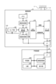
- the imaging device 10 includes a sensor section 100, a sensor control section 101, a visual recognition processing section 102, a memory 103, a recognition processing section 104, an output control section 105, and an interface (I/F) 106. , a data storage unit 130.
- sensor section 100, sensor control section 101, visual recognition processing section 102, memory 103, recognition processing section 104, output control section 105, I/F 106, and data storage section 130 are integrated using, for example, CMOS (Complementary Metal Oxide Semiconductor).
- the sensor is configured as a CMOS image sensor (CIS) formed in the same manner as above.
- the present invention is not limited to this, and some or all of the sensor section 100, sensor control section 101, visual recognition processing section 102, memory 103, recognition processing section 104, output control section 105, I/F 106, and data storage section 130 can be cooperated with each other. It may also be constituted by an independent hardware circuit that operates together.
- the sensor section 100 outputs a pixel signal according to the light irradiated onto the light receiving surface via the optical section 120. More specifically, the sensor unit 100 has a pixel array in which pixels each including at least one photoelectric conversion element are arranged in a matrix. A light-receiving surface is formed by each pixel arranged in rows and columns in the pixel array. The sensor unit 100 further includes a drive circuit for driving each pixel included in the pixel array, and a signal that performs predetermined signal processing on the signal read out from each pixel and outputs it as a pixel signal of each pixel. A processing circuit. The sensor unit 100 outputs a pixel signal of each pixel included in the pixel area as digital image data.
- Frame image data is formed by pixel data based on each pixel signal output from each pixel included in the frame.
- each row in the pixel array of the sensor unit 100 is called a line, and line image data is formed by pixel data based on pixel signals output from each pixel included in the line.
- imaging the operation in which the sensor unit 100 outputs a pixel signal according to the light irradiated onto the light receiving surface.
- the sensor unit 100 controls exposure during imaging and gain (analog gain) for pixel signals in accordance with an imaging control signal supplied from a sensor control unit 101, which will be described later.
- the sensor control unit 101 is configured by a microprocessor, for example, and controls reading of pixel data from the sensor unit 100 according to a program, and outputs pixel data based on each pixel signal read from each pixel included in a frame. . Pixel data output from the sensor control unit 101 is passed to the visual recognition processing unit 102 and the recognition processing unit 104.
- the sensor control unit 101 may control the operations of the visual recognition processing unit 102 and the recognition processing unit 104 according to a program.
- the sensor control unit 101 generates an imaging control signal for controlling imaging in the sensor unit 100.
- the sensor control unit 101 generates an imaging control signal, for example, according to instructions from a visual recognition processing unit 102 and a recognition processing unit 104, which will be described later.
- the imaging control signal includes information indicating the exposure and analog gain during imaging in the sensor unit 100, as described above.
- the imaging control signal further includes control signals (vertical synchronization signal, horizontal synchronization signal, etc.) used by the sensor unit 100 to perform an imaging operation.
- the sensor control unit 101 supplies the generated imaging control signal to the sensor unit 100.
- the optical section 120 is for irradiating the light receiving surface of the sensor section 100 with light from the subject, and is arranged, for example, at a position corresponding to the sensor section 100.
- the optical unit 120 includes, for example, a plurality of lenses, an aperture mechanism for adjusting the size of the aperture for incident light, a focus mechanism for adjusting the focus of the light irradiated onto the light receiving surface, and adjusting the angle of view. and a zoom mechanism for.
- the optical section 120 may further include a shutter mechanism (mechanical shutter) that adjusts the time during which the light receiving surface is irradiated with light.
- the aperture mechanism, focus mechanism, shutter mechanism, and zoom mechanism included in the optical section 120 can be controlled by the sensor control section 101.
- the aperture, focus, and zoom in the optical section 120 can also be controlled from outside the imaging device 10. Further, it is also possible to configure the optical section 120 integrally with the imaging device 10.
- the visual recognition processing unit 102 uses the memory 103 to perform processing on the pixel data passed from the sensor control unit 101 to obtain an image suitable for human viewing. Outputs image data consisting of.
- the visual recognition processing unit 102 includes an ISP (Image Signal Processor), and the visual recognition processing unit 102 is configured by reading and executing a program stored in advance in a memory (not shown) by the ISP.
- the visual recognition processing unit 102 stores image data read from the sensor unit 100 in the memory 103. When a predetermined amount of image data is stored in the memory 103, the visual recognition processing unit 102 performs predetermined image processing on the image data stored in the memory 103.
- the visual recognition processing unit 102 performs demosaic processing. processing, white balance processing, etc. Furthermore, the visual recognition processing unit 102 can instruct the sensor control unit 101 to read pixel data necessary for visual recognition processing from the sensor unit 100. For example, the visibility processing unit 102 may instruct the sensor control unit 101 to read one frame worth of pixel data from the sensor unit 100. Image data whose pixel data has been subjected to image processing by the visual recognition processing unit 102 is passed to the output control unit 105.
- the recognition processing unit 104 Based on the image data passed from the sensor control unit 101, the recognition processing unit 104 performs recognition processing of objects included in the image based on the image data.
- the recognition processing unit 104 includes, for example, a DSP (Digital Signal Processor), and the DSP reads out a program learned in advance by supervised learning or unsupervised learning and stored in the memory 103 as a learning machine learning model. By executing this, recognition processing using DNN (Deep Neural Network) is performed.
- DSP Digital Signal Processor
- the recognition processing unit 104 can instruct the sensor control unit 101 to read pixel data necessary for recognition processing from the sensor unit 100.
- the recognition processing unit 104 instructs the sensor control unit 101 to read pixel data of a designated line (row) from the sensor unit 100.
- the recognition processing unit 104 infers the presence or absence of a foreign object for each line through recognition processing.
- the line-by-line inference results (recognition results) by the recognition processing unit 104 are passed to the output control unit 105.
- the output control unit 105 is configured by, for example, a microprocessor, and sends the inference result of each line passed from the recognition processing unit 104 and the image data passed as the visual recognition processing result from the visual recognition processing unit 102 to the data storage unit 130. hand over.
- the data storage unit 130 includes a memory and stores the inference results for each line passed from the recognition processing unit 104 and the image data passed from the visual recognition processing unit 102.
- the data storage unit 130 can output one or both of the stored inference results and image data to the outside of the imaging device 10, for example, in response to a request from a device external to the imaging device 10. Further, the data storage unit 130 passes the stored image data to the I/F 106 in response to a request from the learning device 20, for example.
- the data storage unit 130 may further pass the stored inference results for each line to the I/F 106.
- the I/F 106 is an interface for transmitting and receiving data, etc., to and from the learning device 20.
- the I/F 106 may be an interface for communicating with the network 2, for example.
- the imaging device 10 is used as a fixed camera with a fixed imaging range, it is preferable that the I/F 106 supports wireless communication, since it is possible to suppress blurring of the imaging range due to contact, impact, or the like.
- the I/F 106 transmits the image data passed from the data storage unit 130 to the learning device 20. Similarly, the I/F 106 transmits the image data passed from the data storage unit 130 to the monitoring device 30. When the I/F 106 receives the inference result for each line from the data storage unit 130, the I/F 106 may transmit the inference result to the learning device 20 or the monitoring device 30.
- the I/F 106 receives data transmitted from the learning device 20.
- the I/F 106 receives a machine learning model transmitted from the learning device 20 and passes the received machine learning model to the recognition processing unit 104.
- the I/F 106 receives information indicating the line number transmitted from the learning device 20 and passes the received information indicating the line number to the sensor control unit 101.
- “information indicating a line number” will be simply referred to as a "line number.”
- the learning device 20 includes a learning section 200, an image storage section 201, a UI (User Interface) section 202, a display section 203, and an interface (I/F) 210.
- the I/F 210 is an interface for transmitting and receiving data, etc., to and from the imaging device 10.
- the I/F 210 receives image data transmitted from the imaging device 10 and passes it to the image storage unit 201.
- the image storage unit 201 stores the image data passed from the I/F 210 in a storage medium such as a memory.
- the learning unit 200 extracts, for example, line image data specified by the UI unit 202 from the image data stored in the image storage unit 201, and uses machine learning, supervised learning or unsupervised learning, to infer the presence or absence of foreign objects. Train and build machine learning models.
- the learning unit 200 transmits the constructed machine learning model to the imaging device 10 from the I/F 210.
- the I/F 106 receives the machine learning model transmitted from the learning device 20, and passes the received machine learning model to the recognition processing unit 104.
- the UI unit 202 constitutes an interface related to user operations.
- the UI unit 202 receives, for example, a user operation on an input device (such as a keyboard) included in the learning device 20. Further, the UI unit 202 generates an image to be presented to the user, and passes the generated image to the display unit 203.
- the display unit 203 generates display control information for displaying the image passed from the UI unit 202 on a display device (not shown).
- the UI unit 202 receives, through a user operation, information about a row number (in some cases, a row number and a column number) indicating a line on which to infer the presence or absence of a foreign object, and the line on which to make the inference is specified.
- the line number for example, the line number increases by 1 for each line, and discrete line numbers are specified. Discrete line numbers mean that one or more unspecified line numbers are included between each specified line number.
- the UI unit 202 transmits the input line number to the imaging device 10 from the I/F 210. In the imaging device 10, the I/F 106 receives the line number transmitted from the learning device 20, and passes the received line number to the recognition processing unit 104.
- FIG. 4 is a schematic diagram showing an example of the hardware configuration of the imaging device 10 according to each embodiment.
- the memory 103, output control section 105, I/F 106, and data storage section 130 are omitted to avoid complexity.
- the data storage section 130 may be configured outside the chip 50.
- the inference result by the recognition processing unit 104 is output to the outside of the chip 50 via an I/F 106 (not shown). Furthermore, in the configuration of FIG. 4, the recognition processing unit 104 can acquire pixel data (line image data) for use in recognition from the sensor control unit 101 via the internal interface of the chip 50.
- the imaging device 10 can be formed on one substrate.
- the present invention is not limited to this, and the imaging device 10 may be a stacked CIS in which a plurality of semiconductor chips are stacked and integrally formed.
- the imaging device 10 can be formed with a two-layer structure in which semiconductor chips are stacked in two layers.
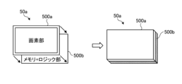
- FIG. 5A is a diagram showing an example in which the imaging device 10 according to each embodiment is formed of a stacked CIS having a two-layer structure.
- a pixel portion 500a is formed in the first layer semiconductor chip
- a memory+logic portion 500b is formed in the second layer semiconductor chip.
- the pixel section 500a includes at least a pixel array in the sensor section 100.
- the memory + logic unit 500b includes, for example, a sensor control unit 101, a recognition processing unit 104, a memory 103, a visual recognition processing unit 102, an output control unit 105, and an I/F 106.
- the memory + logic section 500b further includes part or all of a drive circuit that drives the pixel array in the sensor section 100.
- the imaging device 10 is configured as one solid-state imaging device by bonding the first layer semiconductor chip and the second layer semiconductor chip together while making electrical contact.
- the imaging device 10 can be formed with a three-layer structure in which semiconductor chips are stacked in three layers.
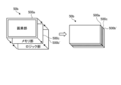
- FIG. 5B is a diagram showing an example in which the imaging device 10 according to each embodiment is formed of a stacked CIS having a three-layer structure.
- a pixel section 500a is formed in the first layer semiconductor chip
- a memory section 500c is formed in the second layer semiconductor chip
- a logic section 500b' is formed in the third layer semiconductor chip.
- the logic section 500b' includes, for example, a sensor control section 101, a recognition processing section 104, a visual recognition processing section 102, an output control section 105, and an I/F 106.
- the memory unit 500c can include the memory 103 and a memory used by the recognition processing unit 104 for recognition processing, for example. The memory may be included in the logic section 500b'.
- the imaging device 10 can be assembled into a single layer. It is configured as one solid-state image sensor.
- FIG. 6 is a block diagram showing the configuration of an example of the sensor unit 100 applicable to each embodiment.
- the sensor unit 100 includes a pixel array unit 1001, a vertical scanning unit 1002, an AD (Analog to Digital) conversion unit 1003, a pixel signal line 1006, a vertical signal line VSL, a control unit 1100, and a signal line A processing unit 1101 is included.
- the control section 1100 and the signal processing section 1101 may be included in the sensor control section 101 shown in FIG. 1, for example.
- the pixel array section 1001 includes a plurality of pixel circuits 1000, each including a photoelectric conversion element such as a photodiode, which performs photoelectric conversion on received light, and a circuit that reads charges from the photoelectric conversion element.
- a plurality of pixel circuits 1000 are arranged in rows and columns in the horizontal direction (row direction) and the vertical direction (column direction).
- the arrangement of pixel circuits 1000 in the row direction is called a line.
- the pixel array section 1001 includes at least 1080 lines in which at least 1920 pixel circuits 1000 are included.
- One frame of image (image data) is formed by pixel signals read from the pixel circuits 1000 included in the frame.
- each line can be identified by a line number.
- the line number can be a number that increases by 1 from one end of the pixel array section 1001 to the other end.
- the line number is "1" for the line r1 on the top end side in the diagram of the pixel array unit 1001, and "2", “3", ..., "1" for each line toward the bottom end. It is added in increments of 1, such as "p".
- the operation of reading out pixel signals from each pixel circuit 1000 included in a frame in the sensor unit 100 will be appropriately described as reading out a pixel from a frame. Further, the operation of reading a pixel signal from each pixel circuit 1000 included in a line included in a frame is appropriately described as reading a line, reading a line image, or the like.
- the row with row number n in the pixel array unit 1001 is described as row r n to distinguish it from row r#n that is randomly designated from the captured image.
- a pixel signal line 1006 is connected to each row and column of each pixel circuit 1000, and a vertical signal line VSL is connected to each column.
- An end of the pixel signal line 1006 that is not connected to the pixel array section 1001 is connected to the vertical scanning section 1002.
- the vertical scanning unit 1002 transmits a control signal such as a drive pulse when reading a pixel signal from a pixel to the pixel array unit 1001 via a pixel signal line 1006 under the control of a control unit 1100 described later.
- An end of the vertical signal line VSL that is not connected to the pixel array section 1001 is connected to the AD conversion section 1003.
- the pixel signal read from the pixel is transmitted to the AD conversion unit 1003 via the vertical signal line VSL.
- the pixel signal is read out from the pixel circuit 1000 by transferring the charge accumulated in the photoelectric conversion element due to exposure to a floating diffusion layer (FD) and converting the transferred charge in the floating diffusion layer into a voltage. conduct.
- a voltage resulting from charge conversion in the floating diffusion layer is output to the vertical signal line VSL via an amplifier.
- the gap between the photoelectric conversion element and the floating diffusion layer is turned off (open), and the photoelectric conversion element generates light in response to incident light by photoelectric conversion. Accumulates electric charge.
- the floating diffusion layer and the vertical signal line VSL are connected in accordance with a selection signal supplied via the pixel signal line 1006. Further, in response to a reset pulse supplied via the pixel signal line 1006, the floating diffusion layer is connected to the power supply voltage VDD or the black level voltage supply line for a short period of time to reset the floating diffusion layer.
- a reset level voltage (referred to as voltage A) of the floating diffusion layer is output to the vertical signal line VSL.
- a transfer pulse supplied via the pixel signal line 1006 turns on (closes) the space between the photoelectric conversion element and the floating diffusion layer, and transfers the charges accumulated in the photoelectric conversion element to the floating diffusion layer.
- a voltage (referred to as voltage B) corresponding to the amount of charge in the floating diffusion layer is output to the vertical signal line VSL.
- the AD conversion unit 1003 includes an AD converter 1007 provided for each vertical signal line VSL, a reference signal generation unit 1004, and a horizontal scanning unit 1005.
- the AD converter 1007 is a column AD converter that performs AD conversion processing on each column of the pixel array section 1001.
- the AD converter 1007 performs AD conversion processing on the pixel signal supplied from the pixel circuit 1000 via the vertical signal line VSL, and performs correlated double sampling (CDS) processing to reduce noise. Two digital values (values corresponding to voltage A and voltage B, respectively) are generated.
- the AD converter 1007 supplies the two generated digital values to the signal processing section 1101.
- the signal processing unit 1101 performs CDS processing based on the two digital values supplied from the AD converter 1007, and generates a pixel signal (pixel data) as a digital signal. Pixel data generated by the signal processing unit 1101 is output to the outside of the sensor unit 100.
- the reference signal generation unit 1004 Based on the control signal input from the control unit 1100, the reference signal generation unit 1004 generates a ramp signal used by each AD converter 1007 to convert a pixel signal into two digital values as a reference signal.
- a ramp signal is a signal whose level (voltage value) decreases at a constant slope over time, or a signal whose level decreases stepwise.
- Reference signal generation section 1004 supplies the generated ramp signal to each AD converter 1007.
- the reference signal generation unit 1004 is configured using, for example, a DAC (Digital to Analog Converter).
- the counter starts counting according to the clock signal.
- the comparator compares the voltage of the pixel signal supplied from the vertical signal line VSL with the voltage of the ramp signal, and stops counting by the counter at the timing when the voltage of the ramp signal crosses the voltage of the pixel signal.
- the AD converter 1007 converts the pixel signal in the form of an analog signal into a digital value by outputting a value corresponding to the count value of the time when counting is stopped.
- the AD converter 1007 supplies the two generated digital values to the signal processing section 1101.
- the signal processing unit 1101 performs CDS processing based on the two digital values supplied from the AD converter 1007, and generates a pixel signal (pixel data) as a digital signal.
- a pixel signal based on a digital signal generated by the signal processing unit 1101 is output to the outside of the sensor unit 100.
- the horizontal scanning unit 1005 performs a selection scan to select each AD converter 1007 in a predetermined order under the control of the control unit 1100, thereby scanning each digital value temporarily held by each AD converter 1007.
- the signals are sequentially output to the signal processing unit 1101.
- the horizontal scanning unit 1005 is configured using, for example, a shift register or an address decoder.
- the control unit 1100 controls the driving of the vertical scanning unit 1002, AD conversion unit 1003, reference signal generation unit 1004, horizontal scanning unit 1005, etc. according to the imaging control signal supplied from the sensor control unit 101.
- the imaging control signal may include a vertical synchronization signal or an external trigger signal, and a horizontal synchronization signal. Further, the imaging control signal may include a row number indicating a row from which pixel signals are read. The imaging control signal may include a column number indicating a column from which pixel signals are read.
- the control unit 1100 generates various drive signals that serve as operating standards for the vertical scanning unit 1002, AD conversion unit 1003, reference signal generation unit 1004, and horizontal scanning unit 1005. For example, the control unit 1100 controls the vertical synchronization signal that the vertical scanning unit 1002 supplies to each pixel circuit 1000 via the pixel signal line 1006 based on the vertical synchronization signal or external trigger signal included in the imaging control signal and the horizontal synchronization signal. Generate control signals. The control unit 1100 supplies the generated control signal to the vertical scanning unit 1002.
- control unit 1100 passes information indicating analog gain, which is included in the imaging control signal supplied from the sensor control unit 101, to the AD conversion unit 1003, for example.
- the AD converter 1003 controls the gain of the pixel signal input to each AD converter 1007 included in the AD converter 1003 via the vertical signal line VSL in accordance with the information indicating the analog gain.
- the vertical scanning unit 1002 sends various signals including drive pulses to the pixel signal line 1006 of the selected pixel row of the pixel array unit 1001 to each pixel circuit 1000 line by line based on the control signal supplied from the control unit 1100. and causes each pixel circuit 1000 to output a pixel signal to the vertical signal line VSL. At this time, the vertical scanning unit 1002 selects pixels from each pixel circuit 1000 in the row r n specified by the row number of the pixel array unit 1001 according to the row number included in the control signal supplied from the control unit 1100. The signal can be read out.
- the vertical scanning unit 1002 is configured using, for example, a shift register or an address decoder. Further, the vertical scanning unit 1002 controls exposure in each pixel circuit 1000 according to information indicating exposure supplied from the control unit 1100.
- control unit 1100 outputs the row number of the row r n for which the vertical scanning unit 1002 is instructed to read pixel signals to the outside of the sensor unit 100 .
- control unit 1100 outputs a column number indicating the column c n from which reading is instructed to the outside of the sensor unit 100 .
- control unit 1100 can selectively output the pixel signals of the specified column, for example, by controlling the output of each AD converter 1007.
- the sensor unit 100 configured in this manner is a column AD type CMOS (Complementary Metal Oxide Semiconductor) image sensor in which AD converters 1007 are arranged in each column.
- CMOS Complementary Metal Oxide Semiconductor
- FIG. 7 is an example functional block diagram for explaining the functions of the recognition processing unit 104 according to the embodiment.
- the learning device 20 generates a line number specifying a line r n to be read from the sensor unit 100 in response to a user operation on the UI unit 202, and transmits the generated line number from the I/F 210 to the imaging device.
- the imaging device 10 receives the row number transmitted from the learning device 20 through the I/F 106, and writes it into the register 107 as setting information for the sensor unit 100.
- the sensor control unit 101 reads setting information from the register 107 and instructs reading of the line r n indicated by the line number indicated in the setting information. Further, the learning device 20 transmits the machine learning model constructed by the learning unit 200 to the imaging device 10 from the I/F 210.
- the recognition processing section 104 includes an inference processing section 140, a line memory 150, and a parameter memory 151.
- the line memory 150 has a capacity that can store at least pixel data included in one line in the sensor section 100.
- the line memory 150 stores pixel data included in one line read from the sensor unit 100 according to the line number read from the register 107 by the sensor control unit 101 and indicated by the line number.
- the parameter memory 151 stores a machine learning model constructed by the learning unit 200, which is transmitted from the learning device 20 and received by the I/F 106.
- line image data pixel data included in one line
- line image data an image based on the line image data
- the inference processing unit 140 includes a processing control unit 141, a first processing unit 142, and a second processing unit 143.
- the processing control section 141 controls the operations of the first processing section 142 and the second processing section 143.
- the first processing unit 142 uses the machine learning model stored in the parameter memory 151 to perform inference processing on the line image data stored in the line memory 150 to determine the presence or absence of foreign objects.
- the inference result of the presence or absence of a foreign object by the first processing unit 142 is passed to the second processing unit 143 together with the line number corresponding to the line image data. Further, the inference result is passed to the output control unit 105 and stored in the data storage unit 130 together with the line number corresponding to the line image data.
- the first processing unit 142 functions as a processing unit that infers the presence or absence of foreign matter for each row based on the pixel signals of pixels included in a designated row among the pixels included in the pixel region.
- the second processing unit 143 uses the inference result from the first processing unit 142 stored in the data storage unit 130 to determine the position of the foreign object. For example, the second processing unit 143 acquires, from the data storage unit 130, the inference result of the line (row) by the first processing unit 142 and the line number of the line (row) from which the inference result was obtained. The second processing unit 143 processes the first processing unit 142 for each line included in the set for a set including three or more consecutive lines (rows) among the rows whose row numbers are specified intermittently. The position of the foreign object in the captured image captured by the sensor unit 100 is determined based on each inference result obtained by the above.
- the second processing unit 143 causes the data storage unit 130 to store information indicating the determined position of the foreign object via the output control unit 105.
- FIG. 8 is a block diagram showing the hardware configuration of an example of the learning device 20 according to the embodiment.
- the learning device 20 includes a CPU (Central Processing Unit) 2000, a ROM (Read Only Memory) 2001, a RAM (Random Access Memory) 2002, a display control unit 2003, a storage device 2004, and a data I/O unit. It includes F2005 and communication I/F2006. In this way, the learning device 20 can have a general computer configuration.
- CPU Central Processing Unit
- ROM Read Only Memory
- RAM Random Access Memory
- the storage device 2004 is a nonvolatile storage medium such as a hard disk drive or flash memory, for example.
- CPU 2000 controls the overall operation of learning device 20 according to programs stored in ROM 2001 and storage device 2004, using RAM 2002 as a work memory.
- the display control unit 2003 generates a display signal that can be handled by the display device 2020 based on the display control information passed from the CPU 2000, and passes it to the display device 2020.
- the display device 2020 includes a display device such as an LCD (Liquid Crystal Display), and a drive circuit for driving the display device.
- the display device 2020 displays an image on the display device according to the display signal passed from the display control unit 2003.
- the data I/F 2005 is an interface for transmitting and receiving data between this learning device 20 and external equipment. Further, an input device 2021 that accepts user operations may be connected to the data I/F 2005.
- the type of input device 2021 is not particularly limited, but a pointing device such as a mouse or a keyboard can be used, for example.
- the UI unit 202 described above may realize a user interface by displaying an image on the input device 2021 and the display device 2020.
- the communication I/F 2006 controls communication of this learning device 20 to the outside.
- the communication I/F 2006 controls communication to the network 2.
- the communication I/F 2006 may directly communicate with the imaging device 10 by wireless communication or the like.
- the CPU 2000 stores the above-mentioned learning unit 200, image storage unit 201, UI unit 202, and display unit 203 in the main memory in the RAM 2002 by executing a program for realizing the functions according to the embodiment.
- Each area is configured, for example, as a module.
- the program can be acquired from the outside via the network 2, for example, by communication via the communication I/F 2006, and installed on the learning device 20.
- the program is not limited to this, and the program may be provided while being stored in a removable storage medium such as a CD (Compact Disk), a DVD (Digital Versatile Disk), or a USB (Universal Serial Bus) memory.
- FIG. 9 is a schematic diagram for schematically explaining the learning process according to the embodiment.
- the machine learning model 90 shown in section (a) of FIG. Ru By inputting the line image data of a designated row r n in the captured image captured by the sensor unit 100 to this machine learning model 90, the presence or absence of a foreign object in the row r n is inferred.
- a machine learning model 91 shown in section (b) of FIG. 9 is constructed by unsupervised learning using images (line images) that do not include foreign objects as learning data.
- the degree of abnormality in the row r n is inferred.
- the degree of abnormality indicates, for example, the degree to which foreign matter is included in the row r n .
- FIGS. 10A and 10B are schematic diagrams for more specifically explaining processing by supervised learning according to the embodiment.
- FIG. 10A is a schematic diagram for explaining the construction process of a machine learning model 90 using supervised learning.
- data in which an abnormality label 92a indicating "no foreign object” is added to an image 45a in which a foreign object (in this example, a person) is not included in the line image of a specified row r n and data in which a foreign object is added to the line image of the specified row r n
- Data obtained by adding an abnormality label 92b indicating "foreign object present" to an image 45b containing "foreign object” is prepared as teacher data.
- the learning unit 200 inputs each prepared teacher data to the machine learning model 90 and causes the machine learning model 90 to learn.
- the learned machine learning model 90 is transmitted from the learning device 20 to the imaging device 10 and stored in the parameter memory 151 in the inference processing unit 140 of the imaging device 10.
- FIG. 10B is a schematic diagram for explaining inference processing by the machine learning model 90 using supervised learning.
- the first processing unit 142 reads the machine learning model 90 stored in the parameter memory 151.
- the first processing unit 142 inputs line image data of a specified row r n stored in the line memory 150 in the line memory 150 in the image 46a that does not include foreign matter in the designated row r n to the machine learning model 90 and performs inference processing. Then, an abnormality label 92 indicating "no foreign matter" is obtained. For example, the first processing unit 142 inputs line image data of a specified row r n stored in the line memory 150 in the image 46b containing a foreign object in the specified row r n to the machine learning model 90 and makes inferences. The process is performed and an abnormality label 92 indicating "foreign object present" is obtained.
- FIG. 11A and FIG. 11B are schematic diagrams for more specifically explaining processing by unsupervised learning according to the embodiment.
- FIG. 11A is a schematic diagram for explaining the construction process of the machine learning model 91 by unsupervised learning.
- an image 45a in which a foreign object (a person in this example) is not included in the line image of the specified row r n is prepared as learning data.
- the learning unit 200 inputs the prepared teacher data to the machine learning model 91 and causes the machine learning model 91 to learn.
- the learned machine learning model 91 is transmitted from the learning device 20 to the imaging device 10 and stored in the parameter memory 151 in the inference processing unit 140 of the imaging device 10.
- FIG. 11B is a schematic diagram for explaining inference processing by the machine learning model 91 using unsupervised learning.
- the first processing unit 142 reads the machine learning model 91 stored in the parameter memory 151.
- the first processing unit 142 inputs line image data of a specified row r n stored in the line memory 150 in the line memory 150, for example , in an image 46a that does not include a foreign object, to the machine learning model 91 and performs inference processing. Then, an abnormality degree 93a indicating a small value (for example, a value below a threshold value) is calculated. Further, for example, the first processing unit 142 inputs line image data of a specified row r n stored in the line memory 150 in the image 46b containing a foreign object in the specified row r n to the machine learning model 91 to make inferences. The processing is performed to calculate an abnormality degree 93b indicating a large value (for example, a value exceeding a threshold value).
- the threshold value for determining the degree of abnormality may be set by machine learning by the learning unit 200, or may be set by the user, for example, by user operation on the learning device 20.
- FIG. 12 is a schematic diagram for explaining determination based on the degree of abnormality calculated by the machine learning model 91 using unsupervised learning, which was explained using FIG. 11B.
- the horizontal axis shows the abnormality degree
- the vertical axis shows the number of calculated abnormality degrees for certain data.
- the magnitude of the degree of abnormality is determined based on the distribution 94a or distribution 94b of the degree of abnormality calculated for certain data.
- the distribution 94a shows an example of the distribution of the degree of abnormality calculated based on the line image data of the line r n without foreign matter specified in the image 46a in FIG. 11B.
- the distribution 94b shows an example of the distribution of the degree of abnormality calculated based on the line image data of the row r n with foreign matter specified in the image 46b in FIG. 11B.
- the first processing unit 142 determines the representative value (maximum value, median value, average value, etc.) of the degree of abnormality in the distribution 94a or the distribution 94b, compares the determined representative value with a threshold value, and determines the degree of abnormality. may be determined. In the example of FIG. 12, the first processing unit 142 determines the degree of abnormality corresponding to the distribution 94a whose representative value is less than or equal to the threshold value to be a small degree of abnormality 93a. On the other hand, the first processing unit 142 determines that the degree of abnormality corresponding to the distribution 94b in which the representative value exceeds the threshold value is a high degree of abnormality 93b.
- FIG. 13 is a schematic diagram for explaining inference processing by the first processing unit 142 according to the embodiment.
- the first processing unit 142 uses a machine learning model based on a CNN (Convolutional Neural Network) 62 to infer the presence or absence of a foreign object in the line image data of the specified row r n .
- CNN Convolutional Neural Network
- the explanation will be given assuming that the CNN 62 is a network based on the machine learning model 90 constructed by the supervised learning described in section (a) of FIG.
- the first processing unit 142 reads from the line memory 150 the line image data of the line image 61 of the line r#n, which is the line number n specified as the inference target, and is included in the image 60 .
- the first processing unit 142 inputs the line image data of the read line image 61 and the line number n of the line image 61 to the CNN 62.
- the CNN 62 performs one-dimensional convolution processing on the line image data of the input line image 61.
- the CNN 62 outputs, for example, an abnormality label 92 indicating "foreign object present" as an analogy result for row r#n, which is row number n.
- the inference processing unit 140 uses the first processing unit 142 to infer the presence or absence of a foreign object based on the one-dimensional spatial feature amount in the horizontal direction in the image 60, for example.
- the inference processing unit 140 outputs the inference result at the time when the inference processing is executed on the line images of all the rows r n designated as inference targets in the image 60 .
- the inference processing unit 140 executes inference processing for each specified row r n in the image 60, it can be said that the inference processing also uses pixel distribution information in the vertical direction of the image 60. That is, when the image 60 has spatial features that differ depending on the vertical position, for example, when the upper half of the image 60 is the sky and the lower half is the ground, predetermined pixel values are assigned to the sky and the ground. The meaning of the pixel value differs depending on which part it is applied to. This means that the vertical pixel distribution information of the image 60 is used.
- the first processing unit 142 after reading the line image data of the specified line r n , the first processing unit 142 reads the line number n of the line and the image data of the read unit (described later) of the line. Input to a machine learning model (CNN62 in this example). The first processing unit 142 uses horizontal spatial information on the line with the line number n and pixel distribution information in the vertical direction with respect to the line based on the input image data of the read unit and the line number n. Then, inference processing is performed for each line and the inference results are output.
- CNN62 machine learning model
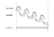
- FIG. 14 is an example sequence diagram for explaining the chronological transition of processing in the first processing unit 142 according to the embodiment.
- the description will be given assuming that rows r#10, r#11, r#12, and r#13 are designated intermittently for the captured image captured by the sensor unit 100.
- the sensor unit 100 reads out the row r#10 from time t 10 to time t 11 , and the line image data of the row r#10 is stored in the line memory 150 .
- the first processing unit 142 reads the line image data of row r#10 from the line memory 150 at time t11 , for example, and executes inference processing by the CNN 62.
- the inference result of the inference process by the CNN 62 is stored in the data storage unit 130 via the output control unit 105, for example, in association with the row number r n of the line r#10.
- the inference result may be expressed as information indicating, for example, the presence or absence of a foreign object as a value "0" or a value "1" for each row.
- the sensor unit 100 reads out the row r#11 from time t 12 to time t 13 , and the line image data of the row r#11 is stored in the line memory 150 .
- the first processing unit 142 reads the line image data of row r#10 from the line memory 150 at time t13 , for example, and executes inference processing by the CNN 62.
- the sensor unit 100 reads out row r#12 from time t 14 to time t 15 , and the first processing unit 142 executes inference processing by CNN 62 from time t 15 and outputs the inference result. do. Furthermore, the sensor unit 100 reads out the row r#13 from time t 16 to time t 17 , and the first processing unit 142 executes inference processing by the CNN 62 from time t 17 and outputs the inference result.
- the latency of inference processing for the captured image captured by the sensor unit 100 is from time t 10 when reading of line image data of the specified first line r#10 from the sensor unit 100 to the specified last line image data. This is the time until time t 20 when the inference processing by the first processing unit 142 for row r#13 is completed.
- inference processing is performed only on line image data of a row specified for a captured image, for example, inference processing is performed using line image data of all rows included in the captured image. Latency can be lower than in the case of
- FIG. 14 shows that the inference process by the CNN 62 in the first processing unit 142 is executed after the reading of one line image data by the sensor unit 100 is completed, this is not applicable to this example. Not limited.
- the sensor unit 100 may read the next line image data while the first processing unit 142 is performing the inference process. By doing so, it is possible to further reduce the latency of inference processing.
- the first processing unit 142 performs inference processing for each line read from the sensor unit 100. Therefore, the computation time required for inference processing can be made substantially constant for each row, and the capacity of memory for holding the computation process can be suppressed.
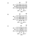
- FIG. 15 is a schematic diagram for explaining possible input units of image data input to a machine learning model that can be applied to the embodiment.
- Section (a) of FIG. 15 is an example in which the entire image 83 of one line specified in the image 82 is used as the input unit of the machine learning model.
- the first processing unit 142 inputs any one of the following four ways shown in (1) to (4) to the machine learning model.
- Image 83 only.
- Image 83 and the line number corresponding to the image 83 (2) Image 83 and the line number corresponding to the image 83.
- Image 83 and the column number corresponding to the image 83 (4) Image 83 and the row number and column number corresponding to the image 83.
- the column numbers of the columns at one end and the other end of the range of interest in the image 83 may be applied.
- Section (b) in FIG. 15 is an example in which an image 84 in a part of one row specified in the image 82 is used as an input unit of the machine learning model.
- the first processing unit 142 inputs any one of the following four ways shown in (5) to (8) to the machine learning model.
- the column number is the column number indicating column c#m-1 of the column at one end of the range corresponding to the image 84 in the row containing the image 84, and the column number at the other end.
- the column number indicating the column c#m+1 may be applied.
- row numbers and column numbers are assigned to the data input to the machine learning model, as in (3), (4), (7), and (8) above.
- the pixel values in the range indicated by the row number and column number it can be determined whether or not the pixel values are normal.
- the range is a range in which a "forest” is imaged, if the pixel value shows "green", it is normal; if it shows a color other than "green” (such as the color of human skin), it is normal.
- FIG. 16 is a schematic diagram for explaining possible output units of image data output from a machine learning model that can be applied to the embodiment.
- Section (a) in FIG. 16 is an example in which the entire image 83 of one line specified in the image 82 is used as the output unit of the inference result.
- the image 84 in a part of one row specified in the image 82 (in this example, the range from columns c#m-1 to c#m+1 in row r#n) is used as the inference result. This is an example of using the output unit.
- section (c) is an example in which a specific pixel 85 in one row specified in the image 82 (in this example, column c#m in row r#n) is the output unit of the inference result. .
- the inference result is "foreign object present” or "no foreign object present”. " is output for each output unit.
- an "abnormality degree” is output for each output unit as an inference result.
- FIG. 17 is a flowchart of an example of inference processing by the inference processing unit 140 according to the embodiment. Note that, prior to the processing according to the flowchart in FIG. 17, one or more rows r#n to be inferred are specified for each row in the frame image, and information indicating each specified row r#n is stored in the register 107. Assume that it is written in .
- step S100 the inference processing unit 140 reads a machine learning model from the parameter memory 151.
- the sensor control unit 101 starts reading frames by the sensor unit 100.
- the sensor control unit 101 reads the line image data of the line designated as the target of analogy processing and indicated by line r#n from the frame, and stores it in the line memory 150. Further, the sensor control unit 101 stores the line number indicating the line of the read line image data in the line memory 150 together with the line image data.
- the sensor control unit 101 stores the specified column number in the line memory 150 together with the line image data and the row number.
- step S103 the inference processing unit 140 uses the first processing unit 142 to acquire line image data from the line memory 150. Further, in step S104, which can be executed in parallel with step S103, the inference processing unit 140 uses the first processing unit 142 to acquire the line number from the line memory 150. If a column number is further specified, the inference processing unit 140 acquires the column number together with the row number in step S104.
- step S103 After the processing in step S103 and step S104, the processing moves to step S105.
- step S105 the first processing unit 142 executes inference processing using the machine learning model on the line image data of the specified row. More specifically, the first processing unit 142 inputs the line number obtained in step S104 and the line image data obtained in step S103 to the machine learning model, and executes the inference process. The first processing unit 142 causes the data storage unit 130 to store the inference result for the line image data of the line indicated by the line number, together with the line number.
- step S106 the inference processing unit 140 determines whether the inference processing for one frame whose reading was started in step S101 has been completed. If the inference processing unit 140 determines that the inference processing for one frame has not been completed (step S106, "No"), the inference processing unit 140 moves the process to step S107, and specifies the next inference target row r#n+1. . After the process in step S107, the process moves to step S102.
- step S106 determines that the inference processing for one frame is completed in step S106 (step S106, "Yes")
- the process moves to step S108.
- step S108 the inference processing unit 140 uses the second processing unit 143 to read out the inference results of each row stored in the data storage unit 130 in step S105, and aggregates the read inference results.
- FIG. 18 is a schematic diagram showing an example of an inference result before the second processing unit 143 performs the aggregation process according to the embodiment.
- rows r#1 to r#7 are designated as targets for inference processing in the captured image 40.
- the first processing unit 142 performs inference processing on each of these rows r#1 to r#7 using a machine learning model, and obtains inference results.
- "no foreign matter” is obtained as the inference result for rows r#1, r#2, r#4, and r#7.
- "foreign object present” is obtained as the inference result for rows #3, r#5, and r#6.
- this erroneous detection is suppressed by determining the position of the foreign object based on the inference result for each row r#n in a set of consecutively specified rows.
- a moving average may be applied to the determination results of each row r#n included in the group.
- Moving average is a method that sets a window with an arbitrary number of samples for multiple aligned samples, moves the window in the alignment direction of the multiple samples, and calculates the average value of the values of the samples included in the window. .
- an inference result of "no foreign object” is represented by a value of "0”
- an inference result of "foreign object present” is represented by a value of "1”
- a moving average value is calculated using an arbitrary number of consecutively designated rows r#nk, . . . , r#n, . . . , r#n+k as a window.
- the calculated moving average value is compared with the threshold value, and if the moving average value exceeds the threshold value, the representative rows r#n ⁇ k, ..., r#n, ..., r#n+k included in the window are A row (for example, row r#n) is determined to have a "foreign object". If the calculated moving average value is less than or equal to the threshold, a representative row among the rows r#n-k, ..., r#n, ..., r#n+k included in the window is determined as "no foreign matter". . While shifting the windows, a moving average is calculated for each window to determine the position of the foreign object in the image.
- the central row r of the plurality of rows r#n ⁇ k, ..., r#n, ..., r#n+k will be used as a representative row. #n can be selected and is preferred.
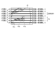
- FIG. 19 is a schematic diagram for more specifically explaining the moving average calculation process of the inference results according to the embodiment.
- the number of samples (number of rows) in the window is set to "3”
- the threshold value for determining presence/absence of foreign matter is set to "0.50”.
- each row r#1 to r#7 corresponds to each row r#1 to r#7 of FIG. 18, respectively.
- a window including three rows r#n-1, r#n, and r#n+1 specified consecutively is set for each row r#1 to r#7, and each row r#n included in the window is A moving average is calculated based on #n-1, r#n, and r#n+1.
- a moving average is calculated for the window including rows r#1, r#2, and r#3.
- the inference result is "no foreign object” and the value is set to "0".
- row r#3 the inference result is "foreign object present", and the value is set to "1".
- the moving average of the inference results for rows r#1, r#2, and r#3 has a value of "0.33", which is less than or equal to the threshold value. Therefore, the second processing unit 143 determines that there is a small possibility that foreign matter exists in the range of rows r#1, r#2, and r#3.
- the window is shifted by one row from section (a), and a moving average is calculated for the window including rows r#2, r#3, and r#4.
- the inference result is "no foreign object” and the value is set to "0".
- row r#3 the inference result is "foreign object present", and the value is set to "1".
- the moving average of the inference results for rows r#2, r#3, and r#4 has a value of "0.33", which is less than or equal to the threshold value. Therefore, the second processing unit 143 determines that there is a small possibility that foreign matter exists in the range of rows r#2, r#3, and r#4.
- the window is shifted by one row from section (b), and a moving average is calculated for the window including rows r#3, r#4, and r#5.
- the inference result is "no foreign object” and the value is set to "0".
- row r#3 the inference result is "foreign object present", and the value is set to "1".
- the moving average of the inference results for rows r#2, r#3, and r#4 has a value of "0.67", which exceeds the threshold value. Therefore, the second processing unit 143 determines that there is a high possibility that foreign matter exists in the range of rows r#2, r#3, and r#4.
- the window is shifted by one row from section (c), and a moving average is calculated for the window including rows r#4, r#5, and r#6.
- row r#4 the inference result is "no foreign matter", and the value is set to "0".
- rows r#5 and r#6 the inference result is "foreign object present", and the value is set to "1", respectively.
- the moving average of the inference results for rows r#4, r#5, and r#6 has a value of "0.67", which exceeds the threshold. Therefore, the second processing unit 143 determines that there is a high possibility that foreign matter exists in the range of rows r#4, r#5, and r#6.
- the inference results of rows r#5 and r#6 are The result of the inference in row r#7 is "there is no foreign substance" and the value is set to "0".
- the moving average of the inference results for rows r#5, r#6, and r#7 has a value of "0.67", which exceeds the threshold value. Therefore, the second processing unit 143 determines that there is a high possibility that foreign matter exists in the range of rows r#5, r#6, and r#7.
- the second processing unit 143 may aggregate these determination results and determine the position of the foreign object in the captured image 40. For example, the second processing unit 143 determines that in the range of rows r#1 to r#4 where it is determined that there is a small possibility that a foreign object exists, the inference result of "foreign object exists" in row r#3 is noise; It may be determined that no foreign matter exists. In addition, the second processing unit 143 also processes rows r#3 to r#7 for which it is determined that there is a high possibility that a foreign object exists, and for which a redundant inference result of "foreign object exists" is obtained. It may be determined that a foreign object exists in the range of #5 and r#6.
- the second processing unit 143 acquires the inference results of each row r#1 to r#7 by the first processing unit 142 from the data storage unit 130.
- the second processing unit 143 calculates the moving average described using FIG. 19 based on the inference results for each row r#1 to r#7 acquired from the data storage unit 130, and Aggregate inference results.
- the second processing unit 143 may cause the data storage unit 130 to store the aggregated inference results.
- FIGS. 20A and 20B are schematic diagrams for explaining a method for aggregating inference results according to the embodiment.
- the inference results for each row r#1 to r#7 specified for the captured image 80 are "no foreign object" for rows r#1 to r#4 and row r#7; 5 and r#6 are assumed to have "foreign matter present”.
- the line image of the line inferred to be "free of foreign matter" is a background image.
- FIG. 20A is an example in which the inference results for each row r#1 to r#7 specified for the captured image 80 are not aggregated, but are output for each row r#1 to r#7.
- the output 95a of the inference processing unit 140 includes information on "no foreign object” and "foreign object present" for each row r#1 to r#7. This output 95a is output from the first processing unit 142, for example.
- the process of step S108 in the flowchart of FIG. 17 can be omitted.
- FIG. 20B is an example in which the inference results of each row r#1 to r#7 specified for the captured image 80 are aggregated and output.
- the output 95b of the inference processing unit 140 indicates that a foreign object exists in the range related to rows r#5 and r#6.
- the second processing unit 143 performs an explanation based on the inference results of each row r#1 to r#7 stored in the data storage unit 130 using FIG. The moving average is calculated, and the inference results for each row r#1 to r#7 are aggregated.
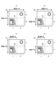
- FIG. 21 is a schematic diagram illustrating an example of setting a region of interest according to the embodiment.
- Section (a) in FIG. 21 is an example in which the entire captured image 80, that is, the range of all rows and columns of the captured image 80, is set as the region of interest.
- regions a and b set in the vertical direction and regions c and d set in the horizontal direction are all set as regions of interest.
- Section (b) in FIG. 21 is an example in which a range of some rows and all columns of the captured image 80 is set as the region of interest.
- the range where region b set in the vertical direction and regions c and d set in the horizontal direction overlap is set as the region of interest.
- the horizontal region c can be set by specifying the column numbers at both ends of the region c in the captured image 80.
- Section (c) in FIG. 21 is an example in which a range of all rows and some columns of the captured image 80 is set as the region of interest.
- the range where areas a and b set in the vertical direction and area c set in the horizontal direction overlap is set as the region of interest.
- Section (d) in FIG. 21 is an example in which a range of some rows and some columns of the captured image 80 is set as the region of interest.
- the range where region b set in the vertical direction and region c set in the horizontal direction overlap is set as the region of interest.
- the first processing unit 142 executes inference processing only within the set attention area.
- the first processing unit 142 does not make inferences outside the region of interest in the captured image 80.
- sections (b) to (d) of FIG. 21 by setting a region of interest indicating an inference range in the captured image 80, it is possible to reduce the load related to inference processing.
- FIG. 22 is a schematic diagram for schematically explaining the technology disclosed in Patent Document 1 as an existing technology.
- Patent Document 1 in order to output the image 72 of the scan line r#n of the output image 73, scan lines r#n-p to scan line r# of the input image 70 are read in units according to the size of the convolution mask. Convolution processing is performed on images of interest 71 up to n+p. Similarly, in order to output the image 75 on the next scan line r#n+1 of the output image 73, the image of interest 74 from the scan line r#n to r#n+p+1 of the input image 70 in the reading unit is convolutioned. Processing is being executed.
- Patent Document 1 after scanning lines are read in order from the top or bottom of the image of interest, convolution processing is performed for each reading unit, and the image is rendered. Therefore, in Patent Document 1, in order to output an image of one scanning line, images of a plurality of scanning lines included in a unit of reading in the input image 70 are stored in a memory.
- FIG. 23 is a schematic diagram for explaining the technology according to the embodiment of the present disclosure in comparison with existing technology.
- the imaging device 10 reads the line image data of the line image 76 of the specified row r#n in the input image 70 as a reading unit.
- the imaging device 10 according to the embodiment infers the presence or absence of a foreign object using the line image data of the line image 76 read in units and a machine learning model learned about the line number or row number and column number of the line image 76.
- the result 76' is output.
- the memory used to execute the inference process only needs to have a capacity that can store one line of image data, and the required memory capacity is smaller than that in Patent Document 1. Furthermore, since the inference result 76' for one line is output based on the line image data of the line image 76 for one line, faster processing is possible than in Patent Document 1.
- convolution processing is performed based on multiple lines of line image data in the input image 70.
- the imaging device uses a rolling shutter method in which exposure is performed line-by-line from an image sensor as an imaging method, rolling distortion occurs in the output image due to different readout timings for each line. In this case, this rolling distortion may affect the convolution process.
- inference processing using a machine learning model is completed in a single line. Therefore, the inference processing according to the embodiment of the present disclosure can eliminate the influence of rolling distortion.
- FIG. 24 is a block diagram showing the configuration of an example of an imaging device according to a modification of the embodiment.
- an imaging device 10a according to a modified example of the embodiment is attached to a fixed object 11 using a fixture 12a, similar to the imaging device 10 according to the embodiment described using FIGS. 3 and 7.
- the fixture 12a applied to the modification of the embodiment includes a movable part 1200 in which the imaging direction and tilt angle of the imaging device 10a are variable. By changing the imaging direction and tilt angle of the imaging device 10a using the attachment 12a, the imaging range of the imaging device 10a can be changed.
- the movable unit 1200 includes a drive unit using, for example, a motor, and by controlling the drive unit, the imaging direction and tilt angle can be changed.
- the movable portion 1200 may change the imaging direction and tilt angle according to control from outside the fixture 12a or according to preset information set in a drive control circuit inside the fixture 12a.
- the movable unit 1200 may change at least one of the imaging direction and the tilt angle at predetermined time intervals in accordance with preset information, thereby switching the imaging range of the imaging device 10a.
- the movable unit 1200 Based on the drive control signal, the movable unit 1200 passes drive information related to changes in the imaging direction and tilt angle to the I/F 106.
- the imaging conditions during imaging can be changed according to a predetermined control signal under the control of the sensor control unit 101.
- the changeable imaging conditions include, for example, zooming by the optical unit 120 (see FIG. 3).
- the sensor control unit 101 may change the imaging conditions according to external control or according to preset information set for the imaging device 10a.
- the sensor control unit 101 passes zoom information indicating the zoom state to the I/F 106.
- the I/F 106 transmits the drive information passed from the movable unit 1200 and the zoom information passed from the sensor control unit 101 to the learning device 20.
- the learning device 20 receives drive information and zoom information transmitted from the imaging device 10a through the I/F 210, and passes the received information to the learning unit 200.
- the learning unit 200 trains a machine learning model using the line image data and row number/column number transmitted from the imaging device 10a, drive information and zoom information, and transmits the learned machine learning model to the I/F 210. from there to the imaging device 10a.
- the imaging device 10a receives the machine learning model learned using the line image data, row number/column number, drive information, and zoom information transmitted from the learning device 20 through the I/F 106, and stores it in the parameter memory 151. Make me remember.
- the first processing unit 142 uses the machine learning model stored in the parameter memory 151 to perform inference processing on the line image data stored in the line memory 150. Thereby, the imaging device 10a can perform inference processing regarding the presence or absence of a foreign object using the imaging direction, tilt angle, and zoom information in addition to the line image data and the row number/column number of the line image data. .
- the present technology can also have the following configuration.
- an imaging unit having a pixel area in which a plurality of pixels are arranged in a matrix, and reading and outputting pixel signals from pixels included in the pixel area; a first processing unit that infers the presence or absence of a foreign object for each row based on the pixel signals of pixels included in a designated row among the pixels included in the pixel region; Equipped with Imaging device.
- the first processing unit includes: Inferring the presence or absence of the foreign object for each row using a model learned using information indicating the designated row and the pixel signal of the pixel included in the designated row; The imaging device according to (1) above.
- the model is a model learned by supervised learning, The imaging device according to (2) above.
- the first model is a model learned by unsupervised learning
- the first processing unit includes: determining the degree of abnormality for each row using the model, and inferring the presence or absence of the foreign object for each row based on the determined degree of abnormality;
- the imaging device is used by being attached to a fixed object using a fixture that can fix the imaging range by the imaging unit,
- the first processing unit includes: When using the imaging device, using the model learned based on the pixel signal output by the imaging unit of the imaging device attached to the fixed object by the mounting tool in the used state, inferring the presence or absence of the foreign object for each row;
- the imaging device according to any one of (2) to (4) above.
- the imaging device is used by being attached to a fixed object using a fixture that allows the imaging range of the imaging unit to be changed according to control
- the first processing unit includes: When the imaging device is used, the imaging device is trained based on the pixel signals output every time the imaging range is changed by the imaging unit of the imaging device attached by the mounting tool in the state of use. using the model for each range change to infer the presence or absence of the foreign object for each row according to the change in the imaging range; The imaging device according to any one of (2) to (4) above.
- the first processing unit includes: When the imaging device is used under predetermined imaging conditions, the model trained in advance based on the pixel signals output by the imaging unit based on the predetermined imaging conditions is used to detect the foreign matter in each row.
- the first processing unit includes: Inferring the presence or absence of the foreign object for each row specified intermittently for the pixel area; The imaging device according to any one of (1) to (7) above. (9) A window including three or more consecutive rows is set for the rows specified intermittently in the pixel area, and the first processing unit removes the foreign matter for each row included in the window. a second processing unit that determines the position of the foreign object based on each inference result in which the presence or absence of the foreign object is inferred; further comprising, The imaging device according to (8) above.
- the second processing unit includes: determining the position of the foreign object based on a moving average of the inference results for each row included in the window; The imaging device according to (9) above.
- the first processing unit includes: inferring the presence or absence of the foreign object for each row specified intermittently in a region of interest set for the pixel region; The imaging device according to any one of (1) to (10) above.
- the first processing unit includes: Inferring the presence or absence of the foreign object for each row based on the pixel signals of pixels included in the specified column in the specified row among the pixels included in the pixel area; The imaging device according to any one of (1) to (11) above.
- the first processing unit includes: inferring the presence or absence of the foreign object in the area specified by the specified row and the specified column;
- a first processing step of inferring the presence or absence of a foreign object for each row based on the pixel signals of pixels included in a designated row among the pixels included in the pixel area; has, Imaging method.
- an imaging step of reading and outputting pixel signals from pixels included in the pixel region by an imaging unit having a pixel region in which a plurality of pixels are arranged in a matrix;
- a first processing step of inferring the presence or absence of a foreign object for each row based on the pixel signals of pixels included in a designated row among the pixels included in the pixel area; Imaging program to run.
Landscapes
- Engineering & Computer Science (AREA)
- Theoretical Computer Science (AREA)
- Physics & Mathematics (AREA)
- General Physics & Mathematics (AREA)
- Multimedia (AREA)
- Computer Vision & Pattern Recognition (AREA)
- General Health & Medical Sciences (AREA)
- Health & Medical Sciences (AREA)
- Signal Processing (AREA)
- Vascular Medicine (AREA)
- Artificial Intelligence (AREA)
- Computing Systems (AREA)
- Databases & Information Systems (AREA)
- Evolutionary Computation (AREA)
- Medical Informatics (AREA)
- Software Systems (AREA)
- Studio Devices (AREA)
- Image Analysis (AREA)
Abstract
Description
1.実施形態
1-1.実施形態の概要
1-2.実施形態に係る構成
1-3.実施形態に係る処理
1-3-1.実施形態に係る学習処理
1-3-2.実施形態に係る推論処理の詳細
1-3-3.注目領域の設定について
1-4.既存技術との対比
2.実施形態の変形例
本開示の実施形態について説明する。本開示の実施形態では、撮像装置として、壁や柱、天井などの固定物に取り付けられ、固定的な撮像範囲で撮像を行う、監視カメラなどの用途に用いられる固定カメラを想定する。実施形態では、当該固定カメラにより撮像された画像において、例えばユーザに指定されたラインごとに、異物の有無を検出する。ユーザは、異物の有無の検出を行うラインを、撮像画像に対して飛び飛びのラインとして指定してよい。
先ず、実施形態の概要ついて説明する。
次に、実施形態に係る構成について説明する。図3は、実施形態に係る撮像装置の一例の構成を示すブロック図である。図3に示されるように、実施形態に係る撮像装置10は、取付具12により天井、壁、柱などの固定物11に取り付けられ、撮像範囲を固定的とされて使用される。
次に、実施形態に係る処理について説明する。
先ず、実施形態に係る学習処理について説明する。図9は、実施形態に係る学習処理を概略的に説明するための模式図である。実施形態では、異常の有無の推論に用いる機械学習モデルとして、図9のセクション(a)に示される、教師あり学習により構築した機械学習モデル90と、同図セクション(b)に示される、教師無し学習により構築した機械学習モデル91と、の何れも適用可能である。
図10Aおよび図10Bは、実施形態に係る教師あり学習による処理をより具体的に説明するための模式図である。
図11Aおよび図11Bは、実施形態に係る教師無し学習による処理をより具体的に説明するための模式図である。
次に、実施形態に適用可能な、第1処理部142での、機械学習モデルにおけるデータの入出力単位について説明する。
(2)画像83と当該画像83に対応する行番号。
(3)画像83と当該画像83に対応する列番号。
(4)画像83と当該画像83に対応する行番号および列番号。
(6)画像84と当該画像84に対応する行番号。
(7)画像84と当該画像84に対応する列番号。
(8)画像84と当該画像84に対応する行番号および列番号。
次に、実施形態に係る推論処理について、より詳細に説明する。
次に、実施形態に係る、撮像画像に対して注目領域を設定し、設定した注目領域を、「異物あり」および「異物無し」の推論を行う推論範囲とする例について説明する。図21は、実施形態に係る注目領域の設定の例を示す模式図である。
次に、本開示の実施形態を、既存技術と対比させて説明する。
次に、実施形態の変形例について説明する。上述した実施形態では、撮像装置10の撮像範囲が固定とされていた。これに対して、実施形態の変形例では、撮像装置10の撮像範囲を可変とした例である。
(1)
複数の画素が行列状の配列で配置された画素領域を有し、前記画素領域に含まれる画素から画素信号を読み出して出力する撮像部と、
前記画素領域に含まれる画素のうち指定された行に含まれる画素の前記画素信号に基づき、前記行ごとに異物の有無を推論する第1処理部と、
を備える、
撮像装置。
(2)
前記第1処理部は、
前記指定された行を示す情報と、前記指定された行に含まれる画素の前記画素信号と、を用いて学習されたモデルを用いて、前記行ごとの前記異物の有無を推論する、
前記(1)に記載の撮像装置。
(3)
前記モデルは、教師あり学習により学習されたモデルである、
前記(2)に記載の撮像装置。
(4)
前期モデルは、教師なし学習により学習されたモデルであって、
前記第1処理部は、
前記モデルを用いて前記行ごとの異常度を求め、求めた該異常度に基づき前記行ごとの前記異物の有無を推論する、
前記(2)に記載の撮像装置。
(5)
当該撮像装置は、前記撮像部による撮像範囲を固定可能な取付具により固定物に取り付けて使用され、
前記第1処理部は、
当該撮像装置を使用する場合に、前記使用する状態で前記取付具により前記固定物に取り付けられた当該撮像装置の前記撮像部により出力された前記画素信号に基づき学習された前記モデルを用いて、前記行ごとの前記異物の有無を推論する、
前記(2)乃至(4)の何れかに記載の撮像装置。
(6)
当該撮像装置は、前記撮像部による撮像範囲を制御に従い変更可能な取付具により固定物に取り付けられて使用され、
をさらに備え、
前記第1処理部は、
当該撮像装置を使用する場合に、前記使用する状態で前記取付具により取り付けられた当該撮像装置の前記撮像部により、前記撮像範囲の変更ごとに出力された前記画素信号に基づき学習された前記撮像範囲の変更ごとの前記モデルを用いて、前記撮像範囲の変更に応じて前記行ごとの前記異物の有無を推論する、
前記(2)乃至(4)の何れかに記載の撮像装置。
(7)
前記第1処理部は、
当該撮像装置を所定の撮像条件で使用する場合に、前記所定の撮像条件に基づき前記撮像部により出力された前記画素信号に基づき予め学習された前記モデルを用いて、前記行ごとの前記異物の有無を推論する、
前記(2)乃至(6)の何れかに記載の撮像装置。
(8)
前記第1処理部は、
前記画素領域に対して飛び飛びに指定された前記行ごとに、前記異物の有無を推論する、
前記(1)乃至(7)の何れかに記載の撮像装置。
(9)
前記画素領域に対して飛び飛びに指定された行に対して、連続して並ぶ3以上の前記行を含む窓を設定し、前記窓に含まれる前記行ごとに前記第1処理部により前記異物の有無が推論された各推論結果に基づき、前記異物の位置を判定する第2処理部、
をさらに備える、
前記(8)に記載の撮像装置。
(10)
前記第2処理部は、
前記窓に含まれる前記行ごとの前記推論結果の移動平均に基づき前記異物の位置を判定する、
前記(9)に記載の撮像装置。
(11)
前記第1処理部は、
前記画素領域に対して設定された注目領域において飛び飛びに指定された前記行ごとに前記異物の有無を推論する、
前記(1)乃至(10)の何れかに記載の撮像装置。
(12)
前記第1処理部は、
前記画素領域に含まれる画素のうち、前記指定された行においてさらに指定された列に含まれる画素の前記画素信号に基づき、前記行ごとの前記異物の有無を推論する、
前記(1)乃至(11)の何れかに記載の撮像装置。
(13)
前記第1処理部は、
前記指定された行および前記指定された列により指定される領域の前記異物の有無を推論する、
前記(12)に記載の撮像装置。
(14)
プロセッサにより実行される、
複数の画素が行列状の配列で配置された画素領域を有する撮像部により、前記画素領域に含まれる画素から画素信号を読み出して出力する撮像ステップと、
前記画素領域に含まれる画素のうち指定された行に含まれる画素の前記画素信号に基づき、前記行ごとに異物の有無を推論する第1処理ステップと、
を有する、
撮像方法。
(15)
プロセッサに、
複数の画素が行列状の配列で配置された画素領域を有する撮像部により、前記画素領域に含まれる画素から画素信号を読み出して出力する撮像ステップと、
前記画素領域に含まれる画素のうち指定された行に含まれる画素の前記画素信号に基づき、前記行ごとに異物の有無を推論する第1処理ステップと、
を実行させるための撮像プログラム。
10,10a 撮像装置
11 固定物
12,12a 取付具
20 学習装置
62 CNN
90,91 機械学習モデル
92,92a,92b 異常ラベル
93a,93b 異常度
94a,94b 分布
95a,95b 出力
96 異物
100 センサ部
101 センサ制御部
102 視認処理部
104 認識処理部
105 出力制御部
106,210 I/F
107 レジスタ
130 データ蓄積部
140 推論処理部
141 処理制御部
142 第1処理部
143 第2処理部
150 ラインメモリ
151 パラメータメモリ
200 学習部
201 画像蓄積部
202 UI部
203 表示部
1000 画素回路
1001 画素アレイ部
1002 垂直走査部
1100 制御部
1200 可動部
Claims (15)
- 複数の画素が行列状の配列で配置された画素領域を有し、前記画素領域に含まれる画素から画素信号を読み出して出力する撮像部と、
前記画素領域に含まれる画素のうち指定された行に含まれる画素の前記画素信号に基づき、前記行ごとに異物の有無を推論する第1処理部と、
を備える、
撮像装置。 - 前記第1処理部は、
前記指定された行を示す情報と、前記指定された行に含まれる画素の前記画素信号と、を用いて学習されたモデルを用いて、前記行ごとの前記異物の有無を推論する、
請求項1に記載の撮像装置。 - 前記モデルは、教師あり学習により学習されたモデルである、
請求項2に記載の撮像装置。 - 前期モデルは、教師なし学習により学習されたモデルであって、
前記第1処理部は、
前記モデルを用いて前記行ごとの異常度を求め、求めた該異常度に基づき前記行ごとの前記異物の有無を推論する、
請求項2に記載の撮像装置。 - 当該撮像装置は、前記撮像部による撮像範囲を固定可能な取付具により固定物に取り付けて使用され、
前記第1処理部は、
当該撮像装置を使用する場合に、前記使用する状態で前記取付具により前記固定物に取り付けられた当該撮像装置の前記撮像部により出力された前記画素信号に基づき学習された前記モデルを用いて、前記行ごとの前記異物の有無を推論する、
請求項2に記載の撮像装置。 - 当該撮像装置は、前記撮像部による撮像範囲を制御に従い変更可能な取付具により固定物に取り付けられて使用され、
をさらに備え、
前記第1処理部は、
当該撮像装置を使用する場合に、前記使用する状態で前記取付具により取り付けられた当該撮像装置の前記撮像部により、前記撮像範囲の変更ごとに出力された前記画素信号に基づき学習された前記撮像範囲の変更ごとの前記モデルを用いて、前記撮像範囲の変更に応じて前記行ごとの前記異物の有無を推論する、
請求項2に記載の撮像装置。 - 前記第1処理部は、
当該撮像装置を所定の撮像条件で使用する場合に、前記所定の撮像条件に基づき前記撮像部により出力された前記画素信号に基づき予め学習された前記モデルを用いて、前記行ごとの前記異物の有無を推論する、
請求項2に記載の撮像装置。 - 前記第1処理部は、
前記画素領域に対して飛び飛びに指定された前記行ごとに、前記異物の有無を推論する、
請求項1に記載の撮像装置。 - 前記画素領域に対して飛び飛びに指定された行に対して、連続して並ぶ3以上の前記行を含む窓を設定し、前記窓に含まれる前記行ごとに前記第1処理部により前記異物の有無が推論された各推論結果に基づき、前記異物の位置を判定する第2処理部、
をさらに備える、
請求項8に記載の撮像装置。 - 前記第2処理部は、
前記窓に含まれる前記行ごとの前記推論結果の移動平均に基づき前記異物の位置を判定する、
請求項9に記載の撮像装置。 - 前記第1処理部は、
前記画素領域に対して設定された注目領域において飛び飛びに指定された前記行ごとに前記異物の有無を推論する、
請求項1に記載の撮像装置。 - 前記第1処理部は、
前記画素領域に含まれる画素のうち、前記指定された行においてさらに指定された列に含まれる画素の前記画素信号に基づき、前記行ごとの前記異物の有無を推論する、
請求項1に記載の撮像装置。 - 前記第1処理部は、
前記指定された行および前記指定された列により指定される領域の前記異物の有無を推論する、
請求項12に記載の撮像装置。 - プロセッサにより実行される、
複数の画素が行列状の配列で配置された画素領域を有する撮像部により、前記画素領域に含まれる画素から画素信号を読み出して出力する撮像ステップと、
前記画素領域に含まれる画素のうち指定された行に含まれる画素の前記画素信号に基づき、前記行ごとに異物の有無を推論する第1処理ステップと、
を有する、
撮像方法。 - プロセッサに、
複数の画素が行列状の配列で配置された画素領域を有する撮像部により、前記画素領域に含まれる画素から画素信号を読み出して出力する撮像ステップと、
前記画素領域に含まれる画素のうち指定された行に含まれる画素の前記画素信号に基づき、前記行ごとに異物の有無を推論する第1処理ステップと、
を実行させるための撮像プログラム。
Priority Applications (2)
| Application Number | Priority Date | Filing Date | Title |
|---|---|---|---|
| US18/847,984 US20250200973A1 (en) | 2022-03-24 | 2023-03-10 | Imaging device, imaging method, and imaging program |
| CN202380027834.9A CN118872282A (zh) | 2022-03-24 | 2023-03-10 | 成像装置、成像方法和成像程序 |
Applications Claiming Priority (2)
| Application Number | Priority Date | Filing Date | Title |
|---|---|---|---|
| JP2022-048481 | 2022-03-24 | ||
| JP2022048481A JP2023141906A (ja) | 2022-03-24 | 2022-03-24 | 撮像装置、撮像方法および撮像プログラム |
Publications (1)
| Publication Number | Publication Date |
|---|---|
| WO2023181981A1 true WO2023181981A1 (ja) | 2023-09-28 |
Family
ID=88101274
Family Applications (1)
| Application Number | Title | Priority Date | Filing Date |
|---|---|---|---|
| PCT/JP2023/009243 Ceased WO2023181981A1 (ja) | 2022-03-24 | 2023-03-10 | 撮像装置、撮像方法および撮像プログラム |
Country Status (4)
| Country | Link |
|---|---|
| US (1) | US20250200973A1 (ja) |
| JP (1) | JP2023141906A (ja) |
| CN (1) | CN118872282A (ja) |
| WO (1) | WO2023181981A1 (ja) |
Families Citing this family (1)
| Publication number | Priority date | Publication date | Assignee | Title |
|---|---|---|---|---|
| JP2025090253A (ja) * | 2023-12-05 | 2025-06-17 | 鹿島建設株式会社 | 充填型鋼管コンクリート柱の監視システム |
Citations (3)
| Publication number | Priority date | Publication date | Assignee | Title |
|---|---|---|---|---|
| JP2014137468A (ja) * | 2013-01-17 | 2014-07-28 | Sony Corp | 撮像装置および撮像方法 |
| JP2020039126A (ja) * | 2018-08-31 | 2020-03-12 | ソニー株式会社 | 撮像装置、撮像システム、撮像方法および撮像プログラム |
| JP2021129265A (ja) * | 2020-02-17 | 2021-09-02 | ソニーセミコンダクタソリューションズ株式会社 | センサ装置、読み出し方法 |
Family Cites Families (1)
| Publication number | Priority date | Publication date | Assignee | Title |
|---|---|---|---|---|
| JPWO2022176686A1 (ja) * | 2021-02-22 | 2022-08-25 |
-
2022
- 2022-03-24 JP JP2022048481A patent/JP2023141906A/ja active Pending
-
2023
- 2023-03-10 US US18/847,984 patent/US20250200973A1/en active Pending
- 2023-03-10 CN CN202380027834.9A patent/CN118872282A/zh not_active Withdrawn
- 2023-03-10 WO PCT/JP2023/009243 patent/WO2023181981A1/ja not_active Ceased
Patent Citations (3)
| Publication number | Priority date | Publication date | Assignee | Title |
|---|---|---|---|---|
| JP2014137468A (ja) * | 2013-01-17 | 2014-07-28 | Sony Corp | 撮像装置および撮像方法 |
| JP2020039126A (ja) * | 2018-08-31 | 2020-03-12 | ソニー株式会社 | 撮像装置、撮像システム、撮像方法および撮像プログラム |
| JP2021129265A (ja) * | 2020-02-17 | 2021-09-02 | ソニーセミコンダクタソリューションズ株式会社 | センサ装置、読み出し方法 |
Also Published As
| Publication number | Publication date |
|---|---|
| JP2023141906A (ja) | 2023-10-05 |
| US20250200973A1 (en) | 2025-06-19 |
| CN118872282A (zh) | 2024-10-29 |
Similar Documents
| Publication | Publication Date | Title |
|---|---|---|
| CN108462844B (zh) | 用于像素合并和读出的方法和装置 | |
| TWI516122B (zh) | 固態成像裝置,固態成像裝置之信號處理方法,及電子設備 | |
| JP4423112B2 (ja) | 固体撮像装置および撮像システム | |
| US20220132068A1 (en) | Imaging device, imaging system, and drive method of imaging device | |
| KR101515654B1 (ko) | 고체 촬상 장치 | |
| US9781366B2 (en) | Image sensing system and method of driving the same | |
| JP2006197393A (ja) | 固体撮像装置、カメラ、及び固体撮像装置の駆動方法 | |
| US20230105329A1 (en) | Image signal processor and image sensor including the image signal processor | |
| JP7356266B2 (ja) | 撮像装置、撮像システム、および撮像装置の駆動方法 | |
| WO2016190116A1 (ja) | 固体撮像装置、固体撮像装置の駆動方法、及び、電子機器 | |
| JP5091695B2 (ja) | 固体撮像装置 | |
| WO2023181981A1 (ja) | 撮像装置、撮像方法および撮像プログラム | |
| JP7753292B2 (ja) | 光電変換装置、移動体、光電変換方法、及びコンピュータプログラム | |
| KR20100047826A (ko) | 고체 촬상 장치 | |
| JP7433792B2 (ja) | 撮像装置およびその制御方法 | |
| JP5589053B2 (ja) | 複数の画素を有するアレイ及び画素情報転送方法 | |
| WO2022255493A1 (ja) | 撮像装置、撮像方法および撮像プログラム | |
| JP2009177741A (ja) | 撮像装置 | |
| JP7433793B2 (ja) | 撮像装置およびその制御方法 | |
| JP7774995B2 (ja) | 光電変換装置、撮像装置、制御方法、及びコンピュータプログラム | |
| JP7492345B2 (ja) | 撮像素子及びその制御方法、及び、撮像装置及びその制御方法 | |
| JP7571173B2 (ja) | 撮像装置、撮像装置の制御方法、及びプログラム | |
| JP2018023637A (ja) | 固体撮像装置、放射線撮像システム及び固体撮像装置の制御方法 | |
| US12192624B2 (en) | Image processing system and operating method thereof | |
| JP7614681B1 (ja) | Ai機能を有する固体撮像装置とその駆動方法、および電子機器 |
Legal Events
| Date | Code | Title | Description |
|---|---|---|---|
| 121 | Ep: the epo has been informed by wipo that ep was designated in this application |
Ref document number: 23774580 Country of ref document: EP Kind code of ref document: A1 |
|
| WWE | Wipo information: entry into national phase |
Ref document number: 202380027834.9 Country of ref document: CN |
|
| WWE | Wipo information: entry into national phase |
Ref document number: 18847984 Country of ref document: US |
|
| NENP | Non-entry into the national phase |
Ref country code: DE |
|
| 122 | Ep: pct application non-entry in european phase |
Ref document number: 23774580 Country of ref document: EP Kind code of ref document: A1 |
|
| WWP | Wipo information: published in national office |
Ref document number: 18847984 Country of ref document: US |