WO2023181593A1 - 電磁波検出器、電磁波検出器アレイ及び画像センサ - Google Patents
電磁波検出器、電磁波検出器アレイ及び画像センサ Download PDFInfo
- Publication number
- WO2023181593A1 WO2023181593A1 PCT/JP2023/000638 JP2023000638W WO2023181593A1 WO 2023181593 A1 WO2023181593 A1 WO 2023181593A1 JP 2023000638 W JP2023000638 W JP 2023000638W WO 2023181593 A1 WO2023181593 A1 WO 2023181593A1
- Authority
- WO
- WIPO (PCT)
- Prior art keywords
- electrode
- electromagnetic wave
- layer
- wave detector
- dimensional material
- Prior art date
- Legal status (The legal status is an assumption and is not a legal conclusion. Google has not performed a legal analysis and makes no representation as to the accuracy of the status listed.)
- Ceased
Links
Images















Classifications
-
- H—ELECTRICITY
- H10—SEMICONDUCTOR DEVICES; ELECTRIC SOLID-STATE DEVICES NOT OTHERWISE PROVIDED FOR
- H10F—INORGANIC SEMICONDUCTOR DEVICES SENSITIVE TO INFRARED RADIATION, LIGHT, ELECTROMAGNETIC RADIATION OF SHORTER WAVELENGTH OR CORPUSCULAR RADIATION
- H10F30/00—Individual radiation-sensitive semiconductor devices in which radiation controls the flow of current through the devices, e.g. photodetectors
- H10F30/20—Individual radiation-sensitive semiconductor devices in which radiation controls the flow of current through the devices, e.g. photodetectors the devices having potential barriers, e.g. phototransistors
-
- H—ELECTRICITY
- H10—SEMICONDUCTOR DEVICES; ELECTRIC SOLID-STATE DEVICES NOT OTHERWISE PROVIDED FOR
- H10F—INORGANIC SEMICONDUCTOR DEVICES SENSITIVE TO INFRARED RADIATION, LIGHT, ELECTROMAGNETIC RADIATION OF SHORTER WAVELENGTH OR CORPUSCULAR RADIATION
- H10F39/00—Integrated devices, or assemblies of multiple devices, comprising at least one element covered by group H10F30/00, e.g. radiation detectors comprising photodiode arrays
- H10F39/10—Integrated devices
- H10F39/12—Image sensors
Definitions
- the present disclosure relates to an electromagnetic wave detector, an electromagnetic wave detector array, and an image sensor.
- Graphene which is an example of a two-dimensional material layer, is known as a material for the electromagnetic wave detection layer used in next-generation electromagnetic wave detectors.
- Graphene has extremely high mobility.
- the absorption rate of graphene is as low as 2.3%. For this reason, methods for increasing the sensitivity of electromagnetic wave detectors using graphene as a two-dimensional material layer have been proposed.
- Patent Document 1 discloses an electromagnetic wave detector including a source electrode, a drain electrode, a graphene layer, and a ferroelectric layer.
- a ferroelectric layer is disposed below or above a graphene layer connected between a source electrode and a drain electrode.
- the ferroelectric layer generates a pyroelectric effect when an incident electromagnetic wave, particularly an electromagnetic wave in an infrared wavelength range, is incident thereon.
- This pyroelectric effect modulates the gate voltage of the graphene layer.
- the graphene layer is atomically thick and has high charge mobility, a small change in gate voltage can produce a huge change in current response. Such an effect is called a light gate effect. High sensitivity can be achieved by this optical gate effect.
- the present disclosure has been made in view of the above problems, and its purpose is to provide an electromagnetic wave detector, an electromagnetic wave detector array, and an image sensor that have higher detection sensitivity and improved off-operation. do.
- An electromagnetic wave detector includes a first ferroelectric layer, a two-dimensional material layer, a first electrode pair, and a second electrode pair.
- the first ferroelectric layer includes a first main surface and has spontaneous polarization.
- a two-dimensional material layer is disposed on the first major surface of the first ferroelectric layer.
- the first electrode pair includes a first electrode and a second electrode.
- the second electrode pair includes a third electrode and a fourth electrode.
- the first electrode pair is electrically connected to the two-dimensional material layer.
- a second electrode pair is electrically connected to the two-dimensional material layer.
- the third electrode and the fourth electrode are arranged facing each other in a first direction perpendicular to the first polarization direction of the spontaneous polarization of the first ferroelectric layer.
- the first electrode and the second electrode are arranged facing each other in a second direction different from the first direction.
- An electromagnetic wave detector array includes a plurality of electromagnetic wave detectors according to the present disclosure.
- a plurality of electromagnetic wave detectors are arranged in line along at least one of a third direction and a fourth direction different from the third direction.
- An image sensor includes an electromagnetic wave detector array according to the present disclosure and a readout circuit connected to the electromagnetic wave detector array according to the present disclosure.
- the electromagnetic wave detector of the present disclosure it is possible to provide an electromagnetic wave detector, an electromagnetic wave detector array, and an image sensor that have higher detection sensitivity and improved off-operation.
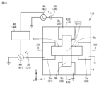
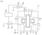
- FIG. 1 is a schematic plan view of an electromagnetic wave detector according to Embodiment 1.
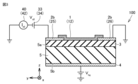
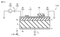
- FIG. 2 is a schematic cross-sectional view of the electromagnetic wave detector according to Embodiment 1 taken along the cross-sectional line II-II shown in FIG. 1.
- FIG. 2 is a schematic cross-sectional view of the electromagnetic wave detector according to Embodiment 1 taken along the cross-sectional line III-III shown in FIG. 1.
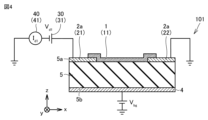
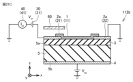
- FIG. 3 is a schematic cross-sectional view showing an electromagnetic wave detector according to a first modification of the first embodiment.
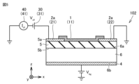
- FIG. 7 is a schematic cross-sectional view showing an electromagnetic wave detector according to a second modification of the first embodiment.
- FIG. 7 is a schematic cross-sectional view showing an electromagnetic wave detector according to a third modification of the first embodiment.
- FIG. 7 is a schematic plan view showing an electromagnetic wave detector according to a fourth modification of the first embodiment.
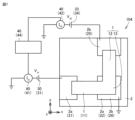
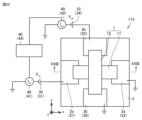
- FIG. 3 is a schematic plan view of an electromagnetic wave detector according to a second embodiment.
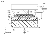
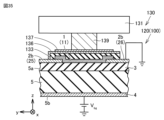
- FIG. 3 is a schematic cross-sectional view of an electromagnetic wave detector according to Embodiment 3.
- FIG. 3 is a schematic cross-sectional view of an electromagnetic wave detector according to Embodiment 3.
- FIG. 7 is a schematic cross-sectional view of an electromagnetic wave detector according to a fourth embodiment.
- FIG. 7 is a schematic cross-sectional view of an electromagnetic wave detector according to a modification of Embodiment 4.
- FIG. 7 is a schematic cross-sectional view of an electromagnetic wave detector according to a fifth embodiment.
- FIG. 3 is a schematic plan view of an electromagnetic wave detector according to a second embodiment.
- FIG. 3 is a schematic cross-sectional view of an electromagnetic wave detector according to Embodiment 3.
- FIG. 3 is a schematic cross-sectional view of an electromagnetic wave detector according to Embod
- FIG. 7 is a schematic cross-sectional view of an electromagnetic wave detector according to a modification of the fifth embodiment.
- FIG. 7 is a schematic cross-sectional view of an electromagnetic wave detector according to a sixth embodiment.
- FIG. 7 is a schematic cross-sectional view of an electromagnetic wave detector according to a seventh embodiment.
- FIG. 7 is a schematic plan view of an electromagnetic wave detector according to Embodiment 8.
- 17 is a schematic cross-sectional view taken along the cross-sectional line XVII-XVII shown in FIG. 16 of an electromagnetic wave detector according to Embodiment 8.
- FIG. 17 is a schematic cross-sectional view of the electromagnetic wave detector according to Embodiment 8, taken along cross-sectional line XVIII-XVIII shown in FIG. 16.
- FIG. 7 is a schematic plan view of an electromagnetic wave detector according to a ninth embodiment.
- 20 is a schematic cross-sectional view of the electromagnetic wave detector according to Embodiment 9 taken along the cross-sectional line XX-XX shown in FIG. 19.
- FIG. 20 is a schematic cross-sectional view of the electromagnetic wave detector according to Embodiment 9 taken along the cross-sectional line XXI-XXI shown in FIG. 19.
- FIG. 10 is a schematic plan view of an electromagnetic wave detector according to a tenth embodiment.
- FIG. 21B is a schematic cross-sectional view of the electromagnetic wave detector according to Embodiment 10 taken along the cross-sectional line XXIC-XXIC shown in FIG. 21B.
- FIG. 7 is a schematic plan view of an electromagnetic wave detector according to an eleventh embodiment.
- 23 is a schematic cross-sectional view of the electromagnetic wave detector according to Embodiment 11 taken along the cross-sectional line XXIII-XXIII shown in FIG. 22.
- FIG. FIG. 12 is a schematic plan view of an electromagnetic wave detector according to a twelfth embodiment.
- 25 is a schematic cross-sectional view of the electromagnetic wave detector according to Embodiment 12, taken along the cross-sectional line XXV-XXV shown in FIG. 24.
- FIG. FIG. 7 is a schematic plan view of an electromagnetic wave detector according to a thirteenth embodiment.
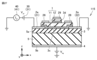
- FIG. 27 is a schematic cross-sectional view of the electromagnetic wave detector according to the thirteenth embodiment taken along the cross-sectional line XXVII-XXVII shown in FIG. 26.
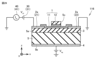
- FIG. FIG. 7 is a schematic plan view of an electromagnetic wave detector according to a fourteenth embodiment. 29 is a schematic cross-sectional view of the electromagnetic wave detector according to the fourteenth embodiment taken along the cross-sectional line XXIX-XXIX shown in FIG. 28.
- FIG. FIG. 7 is a circuit diagram of an electromagnetic wave detector according to a fifteenth embodiment.
- FIG. 7 is a circuit diagram showing an electromagnetic wave detector according to a sixteenth embodiment.
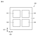
- FIG. 7 is a schematic plan view of an electromagnetic wave detector array according to a seventeenth embodiment.
- FIG. 12 is a schematic plan view showing an electromagnetic wave detector array according to a modification of the seventeenth embodiment.
- FIG. 7 is a schematic partially enlarged view of an image sensor according to a seventeenth embodiment.
- FIG. 7 is a schematic partially enlarged view of an image sensor according to a seventeenth embodiment.
- the figures are schematic and serve to conceptually explain functions or structures. Furthermore, the present disclosure is not limited to the embodiments described below. Unless otherwise specified, the basic configuration of the electromagnetic wave detector is common to all embodiments. Also, items with the same reference numerals are the same or equivalent as described above. This is common throughout the entire specification.
- an electromagnetic wave detector for detecting visible light or infrared light
- the embodiments described below can be used as a detector that detects radio waves such as X-rays, ultraviolet light, near-infrared light, terahertz (THz) waves, and microwaves in addition to visible light and infrared light. is also valid. Note that in the embodiments of the present disclosure, these lights and radio waves are collectively referred to as electromagnetic waves.
- the terms p-type graphene and n-type graphene may be used for graphene.
- graphene with more holes than graphene in the intrinsic state is called p-type graphene
- graphene with more electrons than graphene in the intrinsic state is called n-type graphene.
- the n-type material is a material that has electron donating properties.
- the p-type material is a material that has electron-withdrawing properties.
- n-type when there is a bias in charge throughout the molecule, electrons may be dominant, which is sometimes called n-type. When there is a bias in charge throughout the molecule, holes may be dominant, which is sometimes referred to as p-type.
- an organic substance or an inorganic substance, or a mixture of an organic substance and an inorganic substance may be used.
- plasmon resonance phenomena such as surface plasmon resonance, which is an interaction between a metal surface and light
- pseudo surface plasmon resonance which means resonance on a metal surface in a region other than the visible light region and near-infrared light region.
- metamaterials or plasmonic metamaterials in the sense that wavelengths are manipulated by structures with dimensions smaller than the wavelength, and these are not distinguished by name, but are equivalent in terms of the effects of the phenomena. treated as such.
- These resonances are referred to herein as surface plasmon resonance, plasmon resonance, or simply resonance.
- graphene is mainly used as an example of the material of the two-dimensional material layer, but the material of the two-dimensional material layer is not limited to graphene.
- materials for the two-dimensional material layer include multilayer graphene, turbostratically stacked graphene, transition metal dichalcogenide (TMD), black phosphorus, silicene (a two-dimensional honeycomb structure made of silicon atoms), and germanene. (two-dimensional honeycomb structure made of germanium atoms), etc. can be applied.
- transition metal dichalcogenide include transition metal dichalcogenides such as molybdenum disulfide (MoS 2 ), tungsten disulfide (WS 2 ), and tungsten diselenide (WSe 2 ).
- the two-dimensional material layer is graphene, multilayer graphene, turbostratically stacked graphene, transition metal dichalcogenide (TMD), black phosphorus, or silicene (a two-dimensional honeycomb structure made of silicon atoms). ), graphene nanoribbons, and borophene.
- These materials have a structure similar to graphene.
- atoms are arranged in a single layer in a two-dimensional plane. Therefore, even when these materials are applied to the two-dimensional material layer, the same effects as when graphene is applied to the two-dimensional material layer can be obtained.
- an insulating layer is a layer of an insulating material having a thickness such that no tunnel current occurs.
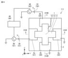
- Embodiment 1 ⁇ Configuration of electromagnetic wave detector 100> An electromagnetic wave detector 100 according to a first embodiment will be described with reference to FIGS. 1 to 3.
- the electromagnetic wave detector 100 includes a first ferroelectric layer 5, a two-dimensional material layer 1, a first electrode pair 2a, a second electrode pair 2b, a first insulating film 3, a back electrode 4, It includes a first operation circuit 30, a second operation circuit 33, and a signal detection circuit 40.
- the first ferroelectric layer 5 includes a first main surface 5a and a second main surface 5b opposite to the first main surface 5a.
- the first main surface 5a and the second main surface 5b each extend in the x direction and the y direction perpendicular to the x direction.
- the normal direction of the first main surface 5a and the normal direction of the second main surface 5b are the z direction perpendicular to the x direction and the y direction.
- the first ferroelectric layer 5 has spontaneous polarization.
- the first polarization direction of the spontaneous polarization of the first ferroelectric layer 5 is, for example, the +x direction.
- the first ferroelectric layer 5 is sensitive to the wavelength of electromagnetic waves irradiated to the electromagnetic wave detector 100 (hereinafter sometimes referred to as "detection wavelength").
- detection wavelength the wavelength of electromagnetic waves irradiated to the electromagnetic wave detector 100
- the first ferroelectric layer 5 absorbs the electromagnetic waves and generates heat. Therefore, the spontaneous polarization of the first ferroelectric layer 5 changes. That is, a pyroelectric effect occurs in the first ferroelectric layer 5.
- electromagnetic waves are irradiated onto electromagnetic wave detector 100 from above in FIGS. 2 and 3. In order to detect electromagnetic waves using the electromagnetic wave detector 100, it is sufficient that the first ferroelectric layer 5 is irradiated with the electromagnetic waves, and the direction in which the electromagnetic waves are irradiated to the electromagnetic wave detector 100 is not particularly limited.
- the first ferroelectric layer 5 is arranged under the two-dimensional material layer 1. Specifically, the first ferroelectric layer 5 is arranged under the first electrode pair 2a, the second electrode pair 2b, and the two-dimensional material layer 1. The first ferroelectric layer 5 may be placed on the two-dimensional material layer 1, or may be placed on the first electrode pair 2a and the second electrode pair 2b. The first main surface 5a of the first ferroelectric layer 5 is covered with the first insulating film 3.
- the two-dimensional material layer 1 is arranged on the first main surface 5a of the first ferroelectric layer 5. As shown in FIGS. 2 and 3, in this embodiment, the two-dimensional material layer 1 is arranged on the first electrode pair 2a and the second electrode pair 2b. The two-dimensional material layer 1 may be arranged under the first electrode pair 2a and the second electrode pair 2b. In a plan view of the first main surface 5a of the first ferroelectric layer 5, the two-dimensional material layer 1 is preferably arranged to overlap the first ferroelectric layer 5. Therefore, the influence of changes in the spontaneous polarization of the first ferroelectric layer 5 on the two-dimensional material layer 1 can be increased.
- the two-dimensional material layer 1 includes a first elongated portion 11 and a second elongated portion 12.
- the first longitudinal direction of the first elongated section 11 is different from the second longitudinal direction of the second elongated section 12.
- the first longitudinal direction of the first elongated portion 11 is, for example, a direction (x direction) parallel to the first polarization direction (+x direction) of the spontaneous polarization of the first ferroelectric layer 5 .
- the second longitudinal direction of the second elongated portion 12 is, for example, the first direction (y direction) perpendicular to the first polarization direction (+x direction) of the spontaneous polarization of the first ferroelectric layer 5 .
- the first elongated portion 11 and the second elongated portion 12 are in the same layer.
- the first elongated portion 11 and the second elongated portion 12 share a common portion 13.
- the common portion 13 is a central portion of the first elongated portion 11 and a central portion of the second elongated portion 12.
- a portion of the first elongated portion 11 overlaps a portion of the second elongated portion 12 in a plan view of the first principal surface 5a.
- the center portion of the first elongated portion 11 overlaps the center portion of the second elongated portion 12 in a plan view of the first principal surface 5a.
- the first elongated portion 11 intersects the second elongated portion 12, and the shape of the two-dimensional material layer 1 is a cross.
- the shape of the two-dimensional material layer 1 in a plan view of the first main surface 5a is not particularly limited, and when the electromagnetic wave detector 100 is irradiated with electromagnetic waves (hereinafter sometimes referred to as "bright state"), the shape of the two-dimensional material layer 1 in a plan view of the first main surface 5a is Any shape may be used as long as a difference occurs between the first electric signal generated from the electrode pair 2a and the second electric signal generated from the second electrode pair 2b.
- the shape of the end of the two-dimensional material layer 1 is rectangular in plan view of the first main surface 5a.
- the shape of the end of the two-dimensional material layer 1 is not particularly limited, and may be triangular or comb-shaped.
- the shape of the first elongated portion 11 between the first electrode 21 and the second electrode 22 is the same as the shape of the second elongated portion 11 between the third electrode 25 and the fourth electrode 26. It is preferable that the shape is the same as that of . If the shape of the first elongated portion 11 between the first electrode 21 and the second electrode 22 is the same as the shape of the second elongated portion 12 between the third electrode 25 and the fourth electrode 26, the first The electrical resistance of the first elongated portion 11 between the electrode 21 and the second electrode 22 is the same as the electrical resistance of the second elongated portion 12 between the third electrode 25 and the fourth electrode 26 .
- the output from the signal detection circuit 40 can be set to zero. Even if the shape of the first elongated portion 11 between the first electrode 21 and the second electrode 22 is different from the shape of the second elongated portion 12 between the third electrode 25 and the fourth electrode 26, By adjusting the signal detection circuit 40, the output from the signal detection circuit 40 can be made zero in the dark state.
- the two-dimensional material layer 1 is formed of, for example, any material selected from the group consisting of graphene, multilayer graphene, turbostratically stacked graphene, transition metal dichalgogenite, black phosphorus, silicene, graphene nanoribbon, and borophene. There is.
- the two-dimensional material layer 1 may be formed of a single monolayer two-dimensional material layer.
- the first electrode pair 2a is electrically connected to the two-dimensional material layer 1. Specifically, the first electrode pair 2 a is electrically connected to the first elongated portion 11 .
- the first electrode pair 2a includes a first electrode 21 and a second electrode 22.
- the first electrode 21 and the second electrode 22 are arranged in a first direction (+x direction) perpendicular to the first polarization direction (+x direction) of the spontaneous polarization of the first ferroelectric layer 5.
- y direction and are arranged opposite to each other in a second direction different from the y direction. Therefore, when the electromagnetic wave detector 100 is irradiated with electromagnetic waves, the electric current of the two-dimensional material layer 1 between the first electrode 21 and the second electrode 22 is caused by a change in the spontaneous polarization of the first ferroelectric layer 5. Resistance changes.
- the second direction is preferably parallel to the first polarization direction (+x direction) of the spontaneous polarization of the first ferroelectric layer 5, and the first electrode 21 and the second electrode 22 are preferably In a plan view of the surface 5a, they are arranged to face each other in the first polarization direction (+x direction) of the spontaneous polarization of the first ferroelectric layer 5. Therefore, the change in electrical resistance of the two-dimensional material layer 1 between the first electrode 21 and the second electrode 22 is maximized.
- the second electrode pair 2b is electrically connected to the two-dimensional material layer 1. Specifically, the second electrode pair 2b is electrically connected to the second elongated portion 12.
- the second electrode pair 2b includes a third electrode 25 and a fourth electrode 26.
- the third electrode 25 and the fourth electrode 26 are arranged in a first direction (y direction) perpendicular to the first polarization direction of the spontaneous polarization of the first ferroelectric layer 5. are placed opposite each other. Therefore, the second electrical signal output from the second electrode pair 2b is not affected by the change in spontaneous polarization of the first ferroelectric layer 5 that occurs in the bright state.
- the electrical resistance of the two-dimensional material layer 1 between the third electrode 25 and the fourth electrode 26 in the bright state is equal to the electrical resistance of the two-dimensional material layer 1 between the third electrode 25 and the fourth electrode 26 in the dark state. Does not change from The second electrical signal output from the second electrode pair 2b does not change between the dark state and the bright state.
- the first electrode 21 and the second electrode 22 are arranged in the first direction (y direction) perpendicular to the first polarization direction (+x direction) of the spontaneous polarization of the first ferroelectric layer 5. ) are arranged opposite to each other in a second direction different from the two directions. Therefore, the first electrical signal output from the first electrode pair 2a is affected by the change in spontaneous polarization of the first ferroelectric layer 5 that occurs in the bright state.
- the electrical resistance of the two-dimensional material layer 1 between the first electrode 21 and the second electrode 22 in the bright state is equal to the electrical resistance of the two-dimensional material layer 1 between the first electrode 21 and the second electrode 22 in the dark state. Changes from The first electrical signal output from the first electrode pair 2a changes between the dark state and the bright state.
- the electrical resistance of the two-dimensional material layer 1 between the first electrode 21 and the second electrode 22 in the dark state is the electrical resistance of the two-dimensional material layer 1 between the third electrode 25 and the fourth electrode 26 in the dark state. be equal to
- the signal detection circuit 40 outputs a difference signal between the first electrical signal output from the first electrode pair 2a and the second electrical signal output from the second electrode pair 2b. Thus, the signal output from the signal detection circuit 40 in the dark state becomes zero.
- the electrical resistance of the two-dimensional material layer 1 between the first electrode 21 and the second electrode 22 changes, but the electrical resistance between the third electrode 25 and the fourth electrode 26 in the dark state changes.
- the electrical resistance of the two-dimensional material layer 1 does not change.
- the signal detection circuit 40 outputs a difference signal between the first electrical signal output from the first electrode pair 2a and the second electrical signal output from the second electrode pair 2b. Therefore, the influence of dark current can be removed from the signal output from the signal detection circuit 40 in the bright state.
- the off-operation of the electromagnetic wave detector 100 is improved.
- the first insulating film 3 is formed on the first main surface 5a of the first ferroelectric layer 5.
- the first insulating film 3 is arranged between the first ferroelectric layer 5 and the two-dimensional material layer 1.
- the first insulating film 3 absorbs electromagnetic waves incident on the electromagnetic wave detector 100 and generates heat. Therefore, the first insulating film 3 can enhance the change in spontaneous polarization of the first ferroelectric layer 5 in the bright state.
- the back electrode 4 is formed on the second main surface 5b of the first ferroelectric layer 5. By applying the back gate voltage V bg to the two-dimensional material layer 1 through the back electrode 4, the back gate voltage V bg can be efficiently applied to the two-dimensional material layer 1.
- the electromagnetic wave detector 100 includes the back electrode 4, it is preferable that the electromagnetic wave is irradiated onto the electromagnetic wave detector 100 from above in FIGS. 2 and 3.
- the first operating circuit 30 is connected to the first electrode pair 2a.
- the first operation circuit 30 includes, for example, a first voltage source 31 that applies a bias voltage V d1 between the first electrode 21 and the second electrode 22.
- the first voltage source 31 applies a bias voltage V d1 to the first elongated portion 11 of the two-dimensional material layer 1 .
- the second operating circuit 33 is connected to the second electrode pair 2b.
- the second operation circuit 33 includes, for example, a second voltage source 34 that applies a bias voltage V d2 between the third electrode 25 and the fourth electrode 26.
- a second voltage source 34 applies a bias voltage V d2 to the second elongated portion 12 of the two-dimensional material layer 1 .
- the signal detection circuit 40 includes a first signal detector 41, a second signal detector 42, and a difference device 44.
- the first signal detector 41 is connected to the first electrode pair 2a. Specifically, the first signal detector 41 is connected to one of the first electrode 21 and the second electrode 22 (in this embodiment, the first electrode 21) included in the first electrode pair 2a. . The other of the first electrode 21 and the second electrode 22 (in this embodiment, the second electrode 22) is, for example, grounded. The first signal detector 41 is connected to the first operating circuit 30 . The first signal detector 41 detects the first electrical signal output from the first electrode pair 2a.
- the first signal detector 41 includes, for example, a first ammeter. In the first ammeter, the first operating circuit 30 applies a bias voltage V d1 between the first electrode 21 and the second electrode 22, so that the first A current I d1 flowing through the elongated portion 11 is detected.
- the second signal detector 42 is connected to the second electrode pair 2b. Specifically, the second signal detector 42 is connected to one of the third electrode 25 and the fourth electrode 26 (in this embodiment, the third electrode 25) included in the second electrode pair 2b. . The other of the third electrode 25 and the fourth electrode 26 (in this embodiment, the fourth electrode 26) is, for example, grounded.
- the second signal detector 42 is connected to the second operating circuit 33.
- the second signal detector 42 detects the second electrical signal output from the second electrode pair 2b.
- the second signal detector 42 includes, for example, a second ammeter. In the second ammeter, the second operating circuit 33 applies a bias voltage V d2 between the third electrode 25 and the fourth electrode 26, so that the second A current I d2 flowing through the elongated portion 12 is detected.
- the difference device 44 is connected to the first signal detector 41 and the second signal detector 42 .
- the differentiator 44 outputs a difference signal between the first electrical signal and the second electrical signal.
- the first electrical signal is the current I d1 flowing through the first elongated portion 11 between the first electrode 21 and the second electrode 22
- the second electrical signal is the current I d1 flowing between the third electrode 25 and the fourth electrode 26.
- the current I d2 flows through the second elongated portion 12 of , and the differentiator 44 outputs a difference signal between the current I d1 and the current I d2 . Therefore, in the dark state, the signal output from the signal detection circuit 40 can be made zero. The influence of dark current can be removed from the signal output from the signal detection circuit 40 in the bright state. The off-operation of the electromagnetic wave detector 100 is improved.
- the two-dimensional material layer 1 is, for example, a single layer of graphene.
- Monolayer graphene is a monoatomic layer of two-dimensional carbon crystals.
- Graphene has a plurality of carbon atoms arranged in each of a plurality of hexagonally arranged chains.
- the absorption rate of graphene is as low as 2.3%.
- the white light absorption rate of graphene is 2.3%. Note that in this embodiment, white light is light in which light having wavelengths of visible light is evenly mixed.
- the two-dimensional material layer 1 may be multilayer graphene in which a plurality of graphene layers are stacked.
- the orientations of the lattice vectors of each hexagonal lattice of graphene in the multilayer graphene may be the same or different. Furthermore, the orientations of the lattice vectors of each hexagonal lattice of graphene in the multilayer graphene may be completely the same. Furthermore, the two-dimensional material layer 1 may be graphene doped with p-type or n-type impurities.
- a band gap is formed in the two-dimensional material layer 1 by stacking two or more graphene layers. That is, the size of the band gap can be adjusted by changing the number of stacked graphene layers.
- the two-dimensional material layer 1 can have a wavelength selection effect of selecting an electromagnetic wave (detection wavelength) to be subjected to photoelectric conversion.
- the mobility of the two-dimensional material layer 1 decreases.
- the noise of the electromagnetic wave detector 100 decreases. Therefore, when multilayer graphene is used as the two-dimensional material layer 1, the absorption of electromagnetic waves in the two-dimensional material layer 1 increases, and the detection sensitivity of the electromagnetic wave detector 100 to electromagnetic waves improves.
- the multilayer graphene may include a turbostratic structure portion.
- the method for producing the turbostratic structure portion may be determined as appropriate.
- a turbostratic structure portion may be formed by transferring a single layer of graphene produced by a CVD method multiple times and stacking multilayer graphene.
- the turbostratic structure portion may be formed by placing ethanol, methane, or the like on the graphene as a carbon source, and growing the graphene by a CVD method.
- normal stacked graphene that does not include a turbostratic structure portion is stacked with the lattices of a plurality of graphene layers aligned with each other.
- Such a stacked state of a plurality of graphene layers is called an AB stack.
- multilayer graphene including a turbostratic structure portion is formed as follows. Graphene created by the CVD method has polycrystals. For this reason, if graphene is further transferred onto the lower layer of graphene multiple times, or if further graphene is stacked using the lower layer of graphene as a core using the CVD method, the lattices of the multiple graphenes become mismatched with each other. Laminated with That is, a turbostratic structure portion is formed in the multilayer graphene. In the turbostratic structure portion, there is little interaction between adjacent graphene layers, and each graphene layer in the turbostratic structure portion has properties equivalent to those of single-layer graphene.
- the mobility of the two-dimensional material layer 1 decreases.
- the graphene in contact with the base is affected by carrier scattering, but the graphene in the upper layer stacked on the graphene in the turbostratic structure is less susceptible to carrier scattering from the base.
- graphene with a turbostratic structure has improved conductivity because there is less interaction between adjacent graphene layers.
- carrier mobility is improved in turbostratic graphene, and the electromagnetic wave detector 100 including turbostratic graphene has improved sensitivity to electromagnetic waves.
- nanoribbon-shaped graphene may be used as the two-dimensional material layer 1.
- the two-dimensional material layer 1 may be a single graphene nanoribbon.
- the two-dimensional material layer 1 may have a structure in which a plurality of graphene nanoribbons are stacked.
- the two-dimensional material layer 1 may have a structure in which graphene nanoribbons are periodically arranged on a plane.
- plasmon resonance is generated in the graphene nanoribbons, so that the sensitivity of the electromagnetic wave detector 100 is improved.
- a structure in which graphene nanoribbons are arranged periodically is sometimes called a graphene metamaterial. In the electromagnetic wave detector 100 using graphene metamaterial as the two-dimensional material layer 1, plasmon resonance is generated, so the sensitivity of the electromagnetic wave detector 100 is improved.
- the ends of the two-dimensional material layer 1 may be graphene nanoribbons.
- the graphene nanoribbon has a band gap, a Schottky junction is formed in the bonding region between the graphene nanoribbon and the electrode.
- the two-dimensional material layer 1 comes into contact with the first electrode pair 2a, carriers are doped into the two-dimensional material layer 1 from the first electrode pair 2a.
- the two-dimensional material layer 1 is made of graphene and the first electrode pair 2a is made of gold (Au)
- the carriers are holes. Due to the difference between the work function of graphene and the work function of gold (Au), holes are doped into the portion of the two-dimensional material layer 1 that is in contact with the first electrode pair 2a.
- the electromagnetic wave detector 100 is driven in an electron conductive state in a state where holes are doped into the corresponding portion of the two-dimensional material layer 1, the mobility of electrons flowing into the channel is reduced due to the influence of the holes. .
- the contact resistance between the two-dimensional material layer 1 and the first electrode pair 2a increases.
- the amount of carriers (doping amount) injected into the two-dimensional material layer 1 from the first electrode pair 2a is large. Therefore, the electron mobility of the electromagnetic wave detector 100 is significantly reduced. Therefore, if all regions of the two-dimensional material layer 1 are formed of single-layer graphene, the performance of the electromagnetic wave detector 100 will deteriorate.
- the amount of carriers doped into the multilayer graphene from the first electrode pair 2a is smaller than the amount of carriers doped into the single layer graphene from the first electrode pair 2a. Therefore, by forming the junction with the first electrode pair 2a, which is easily doped with carriers, from multilayer graphene, an increase in contact resistance between the two-dimensional material layer 1 and the first electrode pair 2a is suppressed. can do. Thereby, a decrease in the mobility of electrons in the electromagnetic wave detector 100 can be suppressed, and the performance of the electromagnetic wave detector 100 can be improved.
- the first electrode pair 2a and the second electrode pair 2b are made of any conductive material.
- the materials of the first electrode pair 2a and the second electrode pair 2b are, for example, gold (Au), silver (Ag), copper (Cu), aluminum (Al), nickel (Ni), chromium (Cr), and palladium. (Pd).
- An adhesion layer (not shown) may be provided between the first electrode pair 2a and the first insulating film 3 and between the second electrode pair 2b and the first insulating film 3.
- the adhesion layer increases the adhesion between the first electrode pair 2a and the first insulating film 3 and the adhesion between the second electrode pair 2b and the first insulating film 3.
- the material of the adhesive layer includes, for example, a metal material such as chromium (Cr) or titanium (Ti).
- the material of the first insulating film 3 is, for example, silicon oxide (SiO 2 ).
- the material of the first insulating film 3 is not limited to silicon oxide, but includes, for example, tetraethyl orthosilicate (Si(OC 2 H 5 ) 4 ), silicon nitride (Si 3 N 4 ), hafnium oxide (HfO 2 ), aluminum oxide ( It may be Al2O3 ), nickel oxide (NiO) , boron nitride (BN), or a siloxane-based polymer material.
- the atomic arrangement of boron nitride (BN) is similar to that of graphene.
- boron nitride (BN) comes into contact with the two-dimensional material layer 1 made of graphene, the decrease in electron mobility of the two-dimensional material layer 1 is suppressed. Therefore, boron nitride (BN) is a suitable material for the first insulating film 3 as a base film disposed under the two-dimensional material layer 1.
- the material of the first insulating film 3 may be a Mott insulator such as ReNiO 3 (Re represents a rare earth element) or TaS 2 .
- a phase transition occurs in the Mott insulator layer, and the physical properties (eg, temperature) of the Mott insulator layer change. Therefore, the Mott insulator layer can enhance the change in spontaneous polarization of the first ferroelectric layer 5 during irradiation with electromagnetic waves.
- the thickness of the first insulating film 3 is such that the first electrode pair 2a and the second electrode pair 2b are electrically insulated with respect to the first ferroelectric layer 5, and the tunnel current is There is no particular restriction as long as it does not occur between and the first ferroelectric layer 5 or between the second electrode pair 2b and the first ferroelectric layer 5.
- the insulating layer does not have to be arranged below the two-dimensional material layer 1.
- the material of the first ferroelectric layer 5 may be any material that causes a change in spontaneous polarization in the first ferroelectric layer 5 when an electromagnetic wave having a detection wavelength is incident on the first ferroelectric layer 5.
- the first ferroelectric layer 5 is made of, for example, barium titanate (BaTiO 3 ), lithium niobate (LiNbO 3 ), lithium tantalate (LiTaO 3 ), strontium titanate (SrTiO 3 ), or lead zirconate titanate.
- the first ferroelectric layer 5 may be formed by laminating or mixing a plurality of different ferroelectric materials.
- the material of the first ferroelectric layer 5 is not limited to the above materials as long as it is a pyroelectric material that exhibits a pyroelectric effect.
- the material of the first ferroelectric layer 5 may be any ferroelectric material that causes a change in spontaneous polarization in response to a change in thermal energy inside the first ferroelectric layer 5. Note that in the pyroelectric effect, electromagnetic waves simply act as a heat source. Therefore, the pyroelectric effect basically has no wavelength dependence, and the first ferroelectric layer 5 basically has no wavelength dependence. Therefore, the first ferroelectric layer 5 is sensitive to broadband electromagnetic waves.
- the material of the first ferroelectric layer 5 has spontaneous polarization.
- the spontaneous polarization of the first ferroelectric layer 5 decreases. Therefore, the electric field applied from the first ferroelectric layer 5 to the two-dimensional material layer 1 is reduced.
- a change in the spontaneous polarization of the first ferroelectric layer 5 causes a change in resistance in the two-dimensional material layer 1 . Therefore, the electromagnetic wave detector 100 including the two-dimensional material layer 1 and the first ferroelectric layer 5 can detect electromagnetic waves.
- the response speed of the electromagnetic wave detector 100 can be improved.
- the thickness of the first ferroelectric layer 5 is determined as much as possible within the range that allows the change in spontaneous polarization of the first ferroelectric layer 5 due to electromagnetic wave irradiation to be exerted on the two-dimensional material layer 1.
- the first ferroelectric layer 5 is preferably a ferroelectric thin film having a thickness of 10 ⁇ m or less.
- the thickness of the first ferroelectric layer 5 is determined by the change in the spontaneous polarization of the first ferroelectric layer 5 when the first ferroelectric layer 5 is irradiated with electromagnetic waves. It is desirable that the thickness be such that it can provide as large a change in electrical resistance as possible.
- a protective film may be provided on the first ferroelectric layer 5.
- the protective film may be provided to cover the two-dimensional material layer 1, the first electrode pair 2a, and the second electrode pair 2b.
- the material of the protective film is, for example, an insulator such as oxide or nitride.
- the material of the protective film is, for example, silicon oxide (SiO 2 ), silicon nitride (SiN), hafnium oxide (HfO 2 ), aluminum oxide (Al 2 O 3 ), or boron nitride (BN).
- An example of the method for manufacturing the electromagnetic wave detector 100 of this embodiment mainly includes a preparation process, a back electrode formation process, an insulating film formation process, an electrode formation process, and a two-dimensional material layer formation process.
- a preparation step is performed.
- a ferroelectric substrate is prepared as the first ferroelectric layer 5.
- the material of the ferroelectric substrate is a material that is sensitive to a predetermined detection wavelength.
- a back electrode forming step is performed.
- a protective film is formed on the surface of the first ferroelectric layer 5 (excluding the second main surface 5b).
- the protective film is, for example, a resist.
- the back electrode 4 is formed on the second main surface 5b of the first ferroelectric layer 5 while the surface of the first ferroelectric layer 5 is protected by a protective film.
- An adhesion layer (not shown) may be formed on the second main surface 5b of the first ferroelectric layer 5 before the back electrode 4 is formed.
- the back electrode forming step may be performed after any step from the insulating film forming step to the two-dimensional material layer forming step, as long as the surface of the first ferroelectric layer 5 is protected by a protective film. .
- the protective film is removed from the surface of the first ferroelectric layer 5.
- an insulating film forming step is performed.
- the first insulating film 3 is formed on the first main surface 5a of the first ferroelectric layer 5.
- the method for forming the first insulating film 3 may be a CVD (Chemical Vapor Deposition) method or a sputtering method.
- the first insulating film 3 may be formed by forming tetraethoxysilane or the like on the first main surface 5a of the first ferroelectric layer 5 using a plasma CVD method or the like.
- an electrode forming step is performed.
- a first electrode pair 2a and a second electrode pair 2b are formed on the first insulating film 3.
- an adhesive layer (not shown) may be formed. The adhesion layer improves the adhesion between the first electrode pair 2a and the first insulating film 3 and the adhesion between the second electrode pair 2b and the first insulating film 3.
- the following process is used as a method for forming the first electrode pair 2a and the second electrode pair 2b.
- a resist mask is formed on the first insulating film 3.
- the resist mask is patterned by a photolithography method or an electron beam (EB) writing method, and openings are formed in regions of the resist mask where the first electrode pair 2a and the second electrode pair 2b are to be formed.
- Ru electron beam
- a conductive film such as a metal film, which will become the first electrode pair 2a and the second electrode pair 2b, is formed on the resist mask using a vapor deposition method, a sputtering method, or the like.
- a conductive film is formed within the opening of the resist mask and on the upper surface of the resist mask.
- the resist mask is removed along with a portion of the conductive film.
- the conductive film in the opening of the resist mask remains on the first insulating film 3, forming a first electrode pair 2a and a second electrode pair 2b on the first insulating film 3.
- the method for forming the first electrode pair 2a and the second electrode pair 2b described above is generally called a lift-off method.
- first electrode pair 2a and the second electrode pair 2b may be formed using other methods.
- a conductive film such as a metal film that becomes the first electrode pair 2a and the second electrode pair 2b is formed on the first insulating film 3.
- a resist mask is formed on the conductive film.
- the resist mask is patterned by photolithography, electron beam (EB) writing, or the like to form openings in the resist mask.
- the resist mask covers the region where the first electrode pair 2a and the second electrode pair 2b are formed, and the opening is formed in the region where the first electrode pair 2a and the second electrode pair 2b are not formed.
- the conductive film is partially removed by wet etching or dry etching using the resist mask as an etching mask.
- the conductive film exposed from the resist mask is removed.
- the conductive film covered by the resist mask remains on the first insulating film 3, forming a first electrode pair 2a and a second electrode pair 2b.
- the resist mask is removed. In this way, the first electrode pair 2a and the second electrode pair 2b may be formed.
- a two-dimensional material layer forming step is performed.
- a two-dimensional material film is formed such that the first electrode pair 2a, the second electrode pair 2b, and the first insulating film 3 are covered with the two-dimensional material layer 1. be done.
- the method of forming the two-dimensional material film is not particularly limited.
- the two-dimensional material film may be formed, for example, by epitaxial growth or by screen printing. Further, the two-dimensional material film may be formed by transferring and pasting a two-dimensional material film previously formed by a CVD method onto the first insulating film 3.
- a two-dimensional material film may be formed by transferring and pasting a film-like two-dimensional material film peeled off by mechanical peeling or the like onto the first insulating film 3.
- a resist mask is formed on the two-dimensional material film.
- the resist mask is patterned by photolithography, electron beam (EB) writing, or the like.
- the resist mask covers a region of the two-dimensional material film where the first electrode pair 2a and the second electrode pair 2b are formed.
- a region of the two-dimensional material film where the first electrode pair 2a and the second electrode pair 2b are not formed is exposed from the resist mask.
- a two-dimensional material film is etched using the resist mask as an etching mask.
- the etching method for the two-dimensional material film is, for example, dry etching using oxygen plasma.
- the resist mask is removed. In this way, a two-dimensional material layer 1 is formed.
- the electromagnetic wave detector 100 of this embodiment is manufactured.
- the two-dimensional material layer 1 was formed on the first electrode pair 2a and the second electrode pair 2b, but the first insulating film 3 or the first ferroelectric layer 5 A two-dimensional material layer 1 may be formed on top, and then a first electrode pair 2a and a second electrode pair 2b may be formed on the two-dimensional material layer 1.
- care must be taken so that the two-dimensional material layer 1 is not damaged by the process of forming the first electrode pair 2a and the second electrode pair 2b. be.
- the first electrode is placed on the two-dimensional material layer 1 exposed from the protective film.
- a pair 2a and a second electrode pair 2b are formed. In this way, damage to the two-dimensional material layer 1 due to the process of forming the first electrode pair 2a and the second electrode pair 2b is suppressed.
- the first voltage source 31 included in the first operating circuit 30 applies a bias voltage V d1 between the first electrode 21 and the second electrode 22 .
- a second voltage source 34 included in the second operating circuit 33 applies a bias voltage V d2 between the third electrode 25 and the fourth electrode 26 .
- a current I d1 flows through the two-dimensional material layer 1 (first elongated portion 11 ) between the first electrode 21 and the second electrode 22 .
- a current I d2 flows through the two-dimensional material layer 1 (second elongated portion 12 ) between the third electrode 25 and the fourth electrode 26 .
- the first ammeter included in the first signal detector 41 detects the current I d1 flowing through the two-dimensional material layer 1 (first elongated portion 11 ) between the first electrode 21 and the second electrode 22 .
- the second ammeter included in the second signal detector 42 detects the current I d2 flowing through the two-dimensional material layer 1 (second elongated portion 12 ) between the third electrode 25 and the fourth electrode 26 .
- Bias voltage V d1 and bias voltage V d2 are adjusted so that current I d1 and current I d2 are equal to each other in the dark state.
- the first ferroelectric layer 5 is irradiated with electromagnetic waves.
- the pyroelectric effect of the first ferroelectric layer 5 causes a change in the spontaneous polarization of the first ferroelectric layer 5 .
- the second direction in which the first electrode 21 and the second electrode 22 face each other is a first direction (y direction). Therefore, the change in spontaneous polarization in the first ferroelectric layer 5 causes a charge density gradient in the two-dimensional material layer 1 between the first electrode 21 and the second electrode 22, and An electric field change is applied to the two-dimensional material layer 1 between the two electrodes 22. Specifically, a change in spontaneous polarization of the first ferroelectric layer 5 occurs in the x direction, and a potential difference is generated between the first electrode 21 and the second electrode 22.
- the two-dimensional material layer 1 enters a state in which a pn junction is formed in a pseudo manner, and the electrical resistance of the two-dimensional material layer 1 between the first electrode 21 and the second electrode 22 changes. This is also called the light gate effect. Due to a change in electrical resistance in the two-dimensional material layer 1 between the first electrode 21 and the second electrode 22, the current I d1 flowing through the two-dimensional material layer 1 between the first electrode 21 and the second electrode 22 changes. do. The current flowing through the two-dimensional material layer 1 when the first ferroelectric layer 5 is irradiated with electromagnetic waves is sometimes referred to as photocurrent.
- the first direction in which the third electrode 25 and the fourth electrode 26 face each other is perpendicular to the first polarization direction (x direction) of the spontaneous polarization of the first ferroelectric layer 5. . Therefore, no polarization change occurs in the first ferroelectric layer 5 in the first direction. No potential difference occurs between the third electrode 25 and the fourth electrode 26, and no electric field change occurs in the two-dimensional material layer 1 between the third electrode 25 and the fourth electrode 26.
- the current I d2 flowing through the two-dimensional material layer 1 between the third electrode 25 and the fourth electrode 26 does not change between the dark state and the bright state. In other words, only the current I d1 changes during electromagnetic wave irradiation.
- the dark current can be made zero, and the photocurrent can be extracted only during electromagnetic wave irradiation. That is, by detecting the difference signal between the current I d1 and the current I d2 , the electromagnetic wave irradiated to the electromagnetic wave detector 100 can be detected.
- the Fermi level of the two-dimensional material layer 1 changes significantly due to the pyroelectric effect of the first ferroelectric layer 5, and a pseudo pn junction is formed within the plane of the two-dimensional material layer 1.
- a potential difference is generated between the first electrode 21 and the second electrode 22, and a current flows through the two-dimensional material layer 1.
- the generated current does not depend on the quantum efficiency of the absorbing material. Therefore, the quantum efficiency of the electromagnetic wave detector 100 exceeds 100%, making it possible to increase the sensitivity of the electromagnetic wave detector 100.
- the electric resistance will increase in the two-dimensional material layer 1 after the electromagnetic wave enters the electromagnetic wave detector 100. Changes take less time to occur. According to such an electromagnetic wave detector 100, delay in amplification due to the optical gate effect is eliminated, and high-speed response of the electromagnetic wave detector 100 becomes possible.
- the first insulating film 3 is omitted, and the first electrode pair 2a and the second electrode pair 2b are It is formed on the first ferroelectric layer 5.
- the first electrode pair 2a and the second electrode pair 2b are formed on the first ferroelectric layer 5.
- the first electrode pair 2a and the second electrode pair 2b are formed on the first main surface 5a of the first ferroelectric layer 5.
- An adhesion layer (not shown) may be formed in the area where the adhesive layer is applied. The adhesion layer improves the adhesion between the first electrode pair 2a and the first ferroelectric layer 5 and the adhesion between the second electrode pair 2b and the first ferroelectric layer 5.
- the electromagnetic wave detector 102 according to the second modification of the present embodiment has the same configuration as the electromagnetic wave detector 101 according to the first modification of the present embodiment, but the substrate 6.
- the substrate 6 is arranged between the first ferroelectric layer 5 and the back electrode 4.
- the substrate 6 includes a main surface 6a and a main surface 6b opposite to the main surface 6a.
- the first ferroelectric layer 5 is formed on the main surface 6a of the substrate 6.
- the second main surface 5b of the first ferroelectric layer 5 faces the main surface 6a of the substrate 6.
- the back electrode 4 is formed on the main surface 6b. If the substrate 6 is made of a semiconductor material such as silicon, the first operating circuit 30, the second operating circuit 33, and the signal detection circuit 40 may be formed on the substrate 6.
- the substrate 6 is prepared.
- a ferroelectric layer forming step is performed following the preparation step.
- the first ferroelectric layer 5 is formed on the substrate 6.
- the method of forming the first ferroelectric layer 5 is not particularly limited.
- the first ferroelectric layer 5 is formed of a ferroelectric polymer material
- a ferroelectric polymer film is formed on the main surface 6a of the substrate 6 by spin coating or the like.
- the ferroelectric polymer film is then patterned by photolithography. In this way, the first ferroelectric layer 5 is formed.
- the first ferroelectric layer 5 is formed. Then, the first ferroelectric layer 5 is patterned by photolithography. In this way, the first ferroelectric layer 5 is formed.
- a lift-off method may be used for patterning the first ferroelectric layer 5. In the lift-off method, a patterned resist mask is formed on the main surface 6a of the substrate 6. Then, the first ferroelectric layer 5 is formed on the resist mask and on the main surface 6a of the substrate 6 exposed from the resist mask. Remove resist mask. In this way, the first ferroelectric layer 5 is patterned.
- the first ferroelectric layer 5 may be formed by bonding a ferroelectric substrate to the substrate 6.
- a ferroelectric substrate For example, an oxide film such as SiO 2 is formed on the substrate 6 and the ferroelectric substrate.
- the oxide film formed on the substrate 6 and the oxide film formed on the ferroelectric substrate are placed opposite each other, and the substrate 6 on which the oxide film is formed and the ferroelectric substrate on which the oxide film is formed are heated. They are bonded to each other by crimping or the like.
- a first ferroelectric layer 5 including a substrate 6 and a ferroelectric substrate bonded to the substrate 6 is obtained. Note that the first ferroelectric layer 5 may be obtained by bonding the ferroelectric substrate to the substrate 6 and then grinding the ferroelectric substrate to make the ferroelectric substrate thinner.
- the first elongated portion 11 is tapered toward the common portion 13 in a plan view of the first main surface 5a. It has a shape.
- the second elongated portion 12 has a tapered shape toward the common portion 13. Therefore, the current I d1 flowing in the first elongated portion 11 between the first electrode 21 and the second electrode 22 becomes difficult to flow into the third electrode 25 and the fourth electrode 26 in the common portion 13 .
- the current I d2 flowing in the second elongated portion 12 between the third electrode 25 and the fourth electrode 26 becomes difficult to flow into the first electrode 21 and the second electrode 22 in the common portion 13 .
- the difference signal between the current I d1 and the current I d2 can be detected more accurately and more easily. In this way, the sensitivity of the electromagnetic wave detector 103a is improved. The off-operation of the electromagnetic wave detector 103a is further improved.
- the first elongated portion 11 extends from the first electrode 21 to the second electrode in a plan view of the first main surface 5a. It has a tapered shape that tapers toward 22. Therefore, the contact area between the first electrode 21 and the first elongated portion 11 is different from the contact area between the second electrode 22 and the first elongated portion 11 .
- the contact resistance between the first electrode 21 and the first elongated section 11 is different from the contact resistance between the second electrode 22 and the first elongated section 11 .
- a temperature gradient occurs in the two-dimensional material layer 1 in the second direction in which the first electrode 21 and the second electrode 22 face each other. This creates a temperature gradient in the first ferroelectric layer 5 in the second direction. When a photocurrent is generated during irradiation with electromagnetic waves, the polarization change of the first ferroelectric layer 5 in the second direction is enhanced.
- the first direction in which the third electrode 25 and the fourth electrode 26 face each other is perpendicular to the first polarization direction (+x direction) of the spontaneous polarization of the first ferroelectric layer 5. .
- the current I d2 flowing through the two-dimensional material layer 1 between the third electrode 25 and the fourth electrode 26 does not change between when electromagnetic waves are irradiated (bright state) and when electromagnetic waves are not irradiated (dark state). Therefore, the difference signal between the current I d1 and the current I d2 increases.
- the difference signal between the current I d1 and the current I d2 can be detected more accurately and more easily. In this way, the sensitivity of the electromagnetic wave detector 103b is improved. The off-operation of the electromagnetic wave detector 103b is further improved.
- the second elongate section 12 has the same shape as the first elongate section 11 .
- the second elongated portion 12 has a tapered shape that tapers from the third electrode 25 toward the fourth electrode 26. Therefore, the current I d2 when the electromagnetic waves are not irradiated is equal to the current I d1 when the electromagnetic waves are not irradiated.
- the signal output from the signal detection circuit 40 can be set to zero. The influence of dark current can be removed from the signal output from the signal detection circuit 40 in the bright state. The off-operation of the electromagnetic wave detector 100 is improved.
- the first elongated portion 11 only needs to generate a temperature gradient in the two-dimensional material layer 1 in the second direction in which the first electrode 21 and the second electrode 22 face each other, and the first elongated portion 11 has a triangular shape. Not limited.
- a temperature gradient may be created in the two-dimensional material layer 1 in the second direction by providing holes in the first elongated portion 11 .
- the first operation circuit 30 may include, for example, a first current source (not shown) that applies a bias current between the first electrode 21 and the second electrode 22. good.
- the first current source applies a bias current to the first elongated portion 11 of the two-dimensional material layer 1 .
- the second operation circuit 33 may include, for example, a second current source (not shown) that applies a bias current between the third electrode 25 and the fourth electrode 26.
- the second current source applies a bias current to the second elongated portion 12 of the two-dimensional material layer 1 .
- the first current source and the second current source are, for example, constant current sources.
- the first signal detector 41 includes, for example, a first voltmeter.
- the first voltmeter detects the voltage generated in the first electrode pair 2a when the first operating circuit 30 applies a bias current between the first electrode 21 and the second electrode 22.
- the second signal detector 42 includes, for example, a second voltmeter.
- the second voltmeter detects the voltage generated in the second electrode pair 2b when the second operating circuit 33 applies a bias current between the third electrode 25 and the fourth electrode 26.
- the difference device 44 outputs a difference signal between the voltage generated at the first electrode pair 2a and the voltage generated at the second electrode pair 2b.
- the sixth modification of the present embodiment has the same configuration as the electromagnetic wave detector 100 of the present embodiment, but the first operating circuit 30 and the second operating circuit 33 may be omitted. Therefore, in the electromagnetic wave detector 100, a change in the current flowing through the two-dimensional material layer 1 between the first electrode 21 and the second electrode 22 occurs only during electromagnetic wave irradiation. Therefore, dark current can be reduced to zero. Noise in the electromagnetic wave detector 100 can be suppressed.
- the current flowing through the two-dimensional material layer 1 between the first electrode 21 and the second electrode 22 is In the electromagnetic wave detector 100 of the form, the current is smaller than the current flowing through the two-dimensional material layer 1 between the first electrode 21 and the second electrode 22.
- the signal output from the signal detection circuit 40 is smaller than that of the electromagnetic wave detector 100 of the present embodiment.
- the seventh modification of the present embodiment has the same configuration as the fifth modification of the present embodiment, but the first operation circuit 30 and the second operation circuit 33 may be omitted. Therefore, in the electromagnetic wave detector 100, a change in the voltage generated at the first electrode pair 2a occurs only during electromagnetic wave irradiation. Therefore, dark current can be reduced to zero. Noise in the electromagnetic wave detector 100 can be suppressed.
- the voltage generated in the two-dimensional material layer 1 between the first electrode 21 and the second electrode 22 is The voltage is smaller than the voltage generated in the two-dimensional material layer 1 between the first electrode 21 and the second electrode 22 in the seventh modification of the embodiment.
- the signal output from the signal detection circuit 40 is smaller than in the fifth modification of the present embodiment.
- the first electrode pair 2a and the second The electrode pair 2b is electrically connected to the two-dimensional material layer 1. Therefore, when the spontaneous polarization of the first ferroelectric layer 5 changes due to the pyroelectric effect, the electrical resistance of the two-dimensional material layer 1 between the first electrode 21 and the second electrode 22 can change. As a result, the conductivity of the two-dimensional material layer 1 is modulated by the photo-gating effect, and the photocurrent can be amplified in the two-dimensional material layer 1.
- the amount of current change in the two-dimensional material layer 1 due to the change in the spontaneous polarization of the first ferroelectric layer 5 is larger than the amount of current change in a normal semiconductor.
- a large current change occurs in response to a slight change in potential.
- the thickness of the two-dimensional material layer 1 is one atomic layer, which is extremely thin.
- the mobility of carriers (for example, electrons or holes) in single-layer graphene is high.
- the amount of current change in the two-dimensional material layer 1 calculated from the carrier mobility in the two-dimensional material layer 1, the thickness of the two-dimensional material layer 1, etc. is several hundred times the amount of current change in a normal semiconductor. ⁇ A few thousand times more.
- the efficiency of extracting current from the two-dimensional material layer 1 is significantly improved.
- Such a photogating effect does not directly enhance the quantum efficiency of the photoelectric conversion material like a normal semiconductor, but increases the current change in the two-dimensional material layer 1 due to electromagnetic wave irradiation. Therefore, the equivalent quantum efficiency of the electromagnetic wave detectors 100, 101, 102, 103a, and 103b calculated from the differential current due to electromagnetic wave irradiation can exceed 100%. Therefore, the electromagnetic wave detection sensitivity of the electromagnetic wave detectors 100, 101, 102, 103a, and 103b according to the present embodiment is the same as that of the conventional semiconductor electromagnetic wave detector and graphene electromagnetic wave detection to which the optical gate effect is not applied. higher than the electromagnetic wave detection sensitivity of the device.
- the current I d1 and the current I d2 are made equal to each other in the dark state, and the current I d1 and the current I d2 are A signal detection circuit 40 detects the difference. Therefore, the electromagnetic wave detectors 100, 101, 102, 103a, and 103b can reduce dark current to zero, and can detect electrical signals only when electromagnetic waves are irradiated. Electromagnetic wave detectors containing graphene have difficulty turning off, resulting in large dark currents and causing noise. In this embodiment, since the dark current can be reduced to zero, even if the electromagnetic wave detectors 100, 101, 102, 103a, 103b contain graphene, noise can be removed from the detection signal output from the signal detection circuit 40. can be reduced.
- the two-dimensional material layer 1 (first elongated portion 11) between the first electrode 21 and the second electrode 22 and the two-dimensional material layer 1 (second elongated portion) between the third electrode 25 and the fourth electrode 26 are also provided.
- variations in the electrical resistance of the two-dimensional material layer 1 that depend on the quality of graphene can be reduced.
- the two-dimensional material layer 1 (first elongated portion 11) between the first electrode 21 and the second electrode 22 and the two-dimensional material layer 1 (second elongated portion) between the third electrode 25 and the fourth electrode 26 are also provided.
- the quantum efficiency of the electromagnetic wave detectors 100, 101, 102, 103a, 103b according to the present embodiment exceeds 100%, and the sensitivity of the electromagnetic wave detectors 100, 101, 102, 103a, 103b to electromagnetic waves is can be improved. Furthermore, the off-operation of the electromagnetic wave detectors 100, 101, 102, 103a, and 103b is improved.
- Embodiment 2 The electromagnetic wave detector 104 according to the second embodiment will be explained with reference to FIG.
- the electromagnetic wave detector 104 of the present embodiment has the same configuration as the electromagnetic wave detector 100 of the first embodiment, and has the same effects, but the electromagnetic wave detector 104 of the first embodiment mainly has the following points. It is different from
- the fourth electrode 26 included in the second electrode pair 2b is the second electrode 22 included in the first electrode pair 2a.
- the first electrode pair 2a and the second electrode pair 2b share one common electrode (second electrode 22, fourth electrode 26).
- the common portion 13 between the first elongated portion 11 and the second elongated portion 12 is one end of the first elongated portion 11 that is close to the second electrode 22, and is located near the fourth electrode 26. This is one end of the second elongated portion 12 that is close to the second elongated portion 12 .
- one end of the first elongated portion 11 overlaps one end of the second elongated portion 12.
- the two-dimensional material layer 1 has an L-shape.
- the two-dimensional material layer 1 (first elongated portion 11) between the first electrode 21 and the second electrode 22 is the two-dimensional material layer 1 (second elongated portion) between the third electrode 25 and the fourth electrode 26. 12) may be made of a different material. Further, one common electrode (second electrode 22, fourth electrode 26) shared by the first electrode pair 2a and the second electrode pair 2b is located between the first electrode 21 and the second electrode 22.
- the first The two-dimensional material layer 1 (first elongated portion 11) between the electrode 21 and the second electrode 22 is the two-dimensional material layer 1 (second elongated portion 12) between the third electrode 25 and the fourth electrode 26.
- the electromagnetic wave detector 104 according to the present embodiment can have fewer electrodes than the electromagnetic wave detector 100 according to the first embodiment. Therefore, the electromagnetic wave detector 104 can realize a simpler configuration.
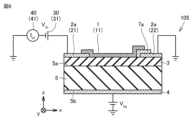
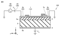
- Electromagnetic wave detector 105 according to Embodiment 3 will be described with reference to FIGS. 8 and 9.
- the electromagnetic wave detector 105 of the present embodiment has the same configuration as the electromagnetic wave detector 100 of the first embodiment, and has the same effects, but is different from the electromagnetic wave detector 100 of the first embodiment mainly in the following points. It's different.
- the electromagnetic wave detector 105 of this embodiment further includes a first semiconductor layer 7a and a second semiconductor layer 7b.
- the first semiconductor layer 7a is arranged between the two-dimensional material layer 1 (first elongated portion 11) and the second electrode 22.
- the second semiconductor layer 7b is arranged between the two-dimensional material layer 1 (second elongated portion 12) and the fourth electrode 26. It is preferable that the first semiconductor layer 7a has the same structure as the second semiconductor layer 7b.
- the electromagnetic wave detector 105 may include only one of the first semiconductor layer 7a and the second semiconductor layer 7b.
- the material of the first semiconductor layer 7a and the second semiconductor layer 7b is, for example, a semiconductor material such as silicon (Si).
- the first semiconductor layer 7a and the second semiconductor layer 7b are made of impurity-doped silicon or the like.
- the material of the first semiconductor layer 7a and the second semiconductor layer 7b may be, for example, germanium (Ge) or a compound semiconductor.
- Compound semiconductors include, for example, silicon carbide (SiC), III-V group semiconductors (gallium nitride (GaN), gallium phosphide (GaP), indium gallium arsenide (InGaAs), indium arsenide (InAs), or iridium antimonide ( or II-V group semiconductors (cadmium mercury telluride (HgCdTe), lead selenium (PbSe), lead sulfur (PbS), or cadmium sulfur (CdS)).
- the semiconductor layer 7 may be formed of a combination of at least two of these semiconductor materials.
- the first semiconductor layer 7a and the second semiconductor layer 7b may have a multilayer structure.
- Semiconductor layer 7 may include quantum wells or quantum dots.
- the material of the semiconductor layer 7 may include a Type II superlattice.
- the first semiconductor layer 7a and the second semiconductor layer 7b may be a pn junction photodiode, a pin photodiode, a Schottky photodiode, or an avalanche photodiode.
- the first semiconductor layer 7a and the second semiconductor layer 7b may be phototransistors.
- the first semiconductor layer 7a and the second semiconductor layer 7b be doped with impurities so that the electrical resistivity of the first semiconductor layer 7a and the second semiconductor layer 7b is 100 ⁇ cm or less.
- the mobility of carriers (holes or electrons) in the first semiconductor layer 7a and the second semiconductor layer 7b is increased. improves. Therefore, the response speed of the electromagnetic wave detector 105 is improved.
- the thickness of the first semiconductor layer 7a and the second semiconductor layer 7b is preferably 10 ⁇ m or less. Since the thicknesses of the first semiconductor layer 7a and the second semiconductor layer 7b are reduced, deactivation of carriers (holes or electrons) in the first semiconductor layer 7a and the second semiconductor layer 7b is reduced.
- an adhesion layer (not shown) may be provided between the second electrode 22 and the first semiconductor layer 7a.
- an adhesion layer (not shown) may be provided between the fourth electrode 26 and the second semiconductor layer 7b.
- the material of the adhesive layer includes, for example, a metal material such as chromium (Cr) or titanium (Ti).
- a Schottky junction is formed between the first semiconductor layer 7a and the two-dimensional material layer 1 (first elongated portion 11).
- a Schottky junction is formed between the second semiconductor layer 7b and the two-dimensional material layer 1 (second elongated portion 12).
- the bias voltage V d1 of the first voltage source 31 and the bias voltage V d2 of the second voltage source 34 are adjusted to apply a reverse bias voltage to the Schottky junction. In this way, the current flowing through the two-dimensional material layer 1 in the dark state can be reduced to zero. That is, dark current can be reduced, and the off-operation of the electromagnetic wave detector 105 is improved.
- the spontaneous polarization of the first ferroelectric layer 5 changes due to the pyroelectric effect, and the Fermi level of the two-dimensional material layer 1 is modulated. Therefore, the energy barrier between the two-dimensional material layer 1 and the first semiconductor layer 7a is lowered. As a result, only when the electromagnetic wave detector 105 is irradiated with electromagnetic waves, a current flows through the first semiconductor layer 7a, and the current I d1 is detected by the first ammeter.
- the amount of change in the current I d1 when the electromagnetic wave detector 105 is irradiated with electromagnetic waves is caused by a change in the electrical resistance of the two-dimensional material layer 1 due to a change in the spontaneous polarization of the first ferroelectric layer 5.
- Electromagnetic wave detector 106 according to Embodiment 4 will be described. Electromagnetic wave detector 106 of this embodiment has the same configuration as electromagnetic wave detector 100 of Embodiment 1, and has similar effects, but it is different from electromagnetic wave detector 100 of Embodiment 1 mainly in the following points. It's different.
- a gap 8 is provided between the first insulating film 3 and the two-dimensional material layer 1.
- the two-dimensional material layer 1 has a portion located apart from the first insulating film 3.
- the two-dimensional material layer 1 has a surface facing the void 8 .
- the gap 8 is provided between the first electrode 21 and the second electrode 22, and also between the third electrode 25 and the fourth electrode 26.
- a pillar (not shown) that supports the two-dimensional material layer 1 may be provided between the two-dimensional material layer 1 and the first insulating film 3. Therefore, the gap 8 can be more reliably formed between the two-dimensional material layer 1 and the first insulating film 3.
- the first insulating film 3 is omitted, similar to the electromagnetic wave detector 101 of the first modification of the first embodiment. ing.
- a gap 8 is provided between the first ferroelectric layer 5 and the two-dimensional material layer 1 .
- a support (not shown) that supports the two-dimensional material layer 1 may be provided between the two-dimensional material layer 1 and the first ferroelectric layer 5. Therefore, the gap 8 can be more reliably formed between the two-dimensional material layer 1 and the first insulating film 3.
- the two-dimensional material layer 1 faces the void 8 as much as possible.
- the thickness of the void 8 is not particularly limited as long as the void 8 can suppress the influence of scattering of carriers on the surface of the first ferroelectric layer 5 or the influence of scattering of carriers on the surface of the first insulating film 3.
- the thickness of the void 8 is preferably as thin as possible. The thinner the gap 8 is, the greater the influence of the electric field from the first ferroelectric layer 5 becomes, and the greater the change in the electrical resistance of the two-dimensional material layer 1 becomes.
- the electromagnetic wave detectors 106 and 107 there is a gap between the first insulating film 3 and the two-dimensional material layer 1 (see FIG. 10) or between the first ferroelectric layer 5 and the two-dimensional material layer 1.
- a gap 8 is provided in between (see FIG. 11). Therefore, the influence of carrier scattering that occurs when the two-dimensional material layer 1 comes into contact with the first insulating film 3 or the first ferroelectric layer 5 can be reduced. As a result, a decrease in carrier mobility in the two-dimensional material layer 1 can be suppressed. Therefore, the sensitivity of the electromagnetic wave detectors 106 and 107 can be improved.
- Embodiment 5 electromagnetic wave detector 108 according to Embodiment 5 will be described.
- the electromagnetic wave detector 108 of this embodiment has the same configuration as the electromagnetic wave detector 102 of the second modification of the first embodiment, and has similar effects, but mainly has the following points compared to the electromagnetic wave detector 102 of the second modification. This is different from the electromagnetic wave detector 102 of the second modification.
- the hole 8b is provided in the substrate 6.
- the hole 8b extends from the main surface 6a to the main surface 6b, and penetrates the substrate 6 in the thickness direction (z direction) of the substrate 6. At least a portion of the second main surface 5b of the first ferroelectric layer 5 is exposed from the substrate 6 in the hole 8b and exposed to the atmosphere surrounding the electromagnetic wave detector 108.
- the hole 8b overlaps the two-dimensional material layer 1.
- the hole 8b is provided below the two-dimensional material layer 1.
- substrate 6 is omitted, similar to electromagnetic wave detector 101 of the first modification of Embodiment 1.
- a recess 8c is provided in the second main surface 5b of the first ferroelectric layer 5. At least a portion of the second main surface 5b of the first ferroelectric layer 5 is exposed from the back electrode 4 in the recess 8c and exposed to the atmosphere surrounding the electromagnetic wave detector 108b.
- the recess 8c overlaps the two-dimensional material layer 1.
- the recess 8c is provided below the two-dimensional material layer 1.
- the heat insulation performance of the first ferroelectric layer 5 is improved, and heat radiation after electromagnetic wave irradiation can be suppressed.
- the change in spontaneous polarization of the first ferroelectric layer 5 can be increased. Therefore, the sensitivity of the electromagnetic wave detectors 108, 108b can be improved.
- electromagnetic wave detector 109 With reference to FIG. 14, electromagnetic wave detector 109 according to Embodiment 6 will be described.
- the electromagnetic wave detector 109 of the present embodiment has the same effects as the electromagnetic wave detector 102 of the second modification of the first embodiment, and has similar effects, but the electromagnetic wave detector 109 of the present embodiment has the following points. This is different from the electromagnetic wave detector 102 of the second modification.
- the thickness of the first ferroelectric layer 5 changes between the first electrode 21 and the second electrode 22. Between the first electrode 21 and the second electrode 22, the height of the first main surface 5a changes.
- the first ferroelectric layer 5 includes a first ferroelectric layer portion 51 and a second ferroelectric layer portion 52. In a plan view of the first main surface 5a, the first ferroelectric layer portion 51 is placed on the first electrode 21 side, and the second ferroelectric layer portion 52 is placed on the second electrode 22 side. There is.
- the first ferroelectric layer portion 51 and the second ferroelectric layer portion 52 are arranged in a second direction (for example, the x direction) in which the first electrode 21 and the second electrode 22 face each other. .
- the thickness of the second ferroelectric layer portion 52 is different from the thickness of the first ferroelectric layer portion 51.
- the second ferroelectric layer portion 52 is thinner than the first ferroelectric layer portion 51.
- a step 55 is formed at the boundary between the first ferroelectric layer portion 51 and the second ferroelectric layer portion 52.
- the second main surface 5b of the first ferroelectric layer 5 is flush with the first ferroelectric layer portion 51 and the second ferroelectric layer portion 52.
- the first elongated portion 11 of the two-dimensional material layer 1 is arranged on the first ferroelectric layer portion 51 and the second ferroelectric layer portion 52.
- the two-dimensional material layer 1 covers the step 55.
- the first ferroelectric layer 5 is preferably configured so that no change in spontaneous polarization occurs between the third electrode 25 and the fourth electrode 26. Therefore, for example, in the first ferroelectric layer 5 located between the third electrode 25 and the fourth electrode 26 in a plan view of the first principal surface 5a, the third electrode 25 and the fourth electrode 26 are spaced apart from each other.
- the first ferroelectric layer may have a constant structure in the direction of polarization, and a symmetrical structure in the direction of spontaneous polarization of the first ferroelectric layer.
- the first ferroelectric layer 5 is configured such that no change in spontaneous polarization occurs between the third electrode 25 and the fourth electrode 26, the first ferroelectric layer portion 51 and the second ferroelectric layer portion 51
- the polarization direction of the dielectric layer portion 52 may not be in the x direction, but may be in the z direction, for example.
- the first ferroelectric layer 5 may include three or more ferroelectric layer portions having mutually different thicknesses. Between the first electrode 21 and the second electrode 22, the thickness of the first ferroelectric layer 5 may change continuously, and the first main surface 5a of the first ferroelectric layer 5 is It may be inclined with respect to the second main surface 5b of the ferroelectric layer 5.
- the thickness of the first ferroelectric layer 5 changes between the first electrode 21 and the second electrode 22.
- the amount of voltage change that occurs in the two-dimensional material layer 1 due to the pyroelectric effect of the first ferroelectric layer 5 also changes. That is, the amount of voltage change that occurs in the two-dimensional material layer 1 on the portion of the first ferroelectric layer 5 having a larger thickness (the first ferroelectric layer portion 51) is greater than that on the first ferroelectric layer 5 having a smaller thickness. This is different from the amount of voltage change that occurs in the two-dimensional material layer 1 located on the portion of the ferroelectric layer 5 (second ferroelectric layer portion 52).
- the voltage applied to the two-dimensional material layer 1 on the part of the first ferroelectric layer 5 having a larger thickness is applied to the first ferroelectric layer 5 having a smaller thickness. It is different from the voltage applied to the two-dimensional material layer 1 on the portion of the ferroelectric layer 5 (second ferroelectric layer portion 52).
- a pseudo pn junction is formed in the two-dimensional material layer 1, and the efficiency of extracting current from the two-dimensional material layer 1 is improved.
- the influence of changes in the spontaneous polarization of the first ferroelectric layer 5 on the two-dimensional material layer 1 increases. Therefore, the detection sensitivity of the electromagnetic wave detector 109 is improved.
- Embodiment 7 With reference to FIG. 15, an electromagnetic wave detector 110 according to Embodiment 7 will be described.
- the electromagnetic wave detector 110 according to the present embodiment has the same configuration as the electromagnetic wave detector 100 according to the first embodiment, and has similar effects, but is different from the electromagnetic wave detector 100 according to the first embodiment mainly in the following points. It's different.
- the dielectric constant of the first ferroelectric layer 5 changes between the first electrode 21 and the second electrode 22.
- the first ferroelectric layer 5 includes a first ferroelectric layer portion 51 and a second ferroelectric layer portion 52.
- the first ferroelectric layer portion 51 is placed on the first electrode 21 side
- the second ferroelectric layer portion 52 is placed on the second electrode 22 side.
- the first ferroelectric layer portion 51 and the second ferroelectric layer portion 52 are arranged in a second direction (for example, the x direction) in which the first electrode 21 and the second electrode 22 face each other.
- the dielectric constant of the first ferroelectric layer portion 51 is different from the dielectric constant of the second ferroelectric layer portion 52.
- the ferroelectric material forming the first ferroelectric layer portion 51 is different from the ferroelectric material forming the second ferroelectric layer portion 52.
- the absorption wavelength range of the first ferroelectric layer portion 51 may be different from the absorption wavelength range of the second ferroelectric layer portion 52.
- the first elongated portion 11 of the two-dimensional material layer 1 is arranged on the first ferroelectric layer portion 51 and the second ferroelectric layer portion 52.
- the first ferroelectric layer 5 is preferably configured so that no change in spontaneous polarization occurs between the third electrode 25 and the fourth electrode 26.
- the first ferroelectric layer 5 may include three or more ferroelectric layer portions having mutually different polarizabilities. Further, as long as the first ferroelectric layer 5 is configured such that no change in spontaneous polarization occurs between the third electrode 25 and the fourth electrode 26, the first ferroelectric layer portion 51 and the second ferroelectric layer portion 51
- the polarization direction of the dielectric layer portion 52 may not be in the x direction, but may be in the z direction, for example.
- the dielectric constant of the first ferroelectric layer portion 51 is different from the dielectric constant of the second ferroelectric layer portion 52.
- the amount of voltage change that occurs in the two-dimensional material layer 1 due to the pyroelectric effect of the ferroelectric material also differs. That is, the amount of voltage change that occurs in the two-dimensional material layer 1 on the first ferroelectric layer portion 51 is different from the amount of voltage change that occurs on the two-dimensional material layer 1 on the second ferroelectric layer portion 52.
- the voltage applied to the two-dimensional material layer 1 on the first ferroelectric layer portion 51 is different from the voltage applied to the two-dimensional material layer 1 on the second ferroelectric layer portion 52; A pseudo pn junction is formed in the dimensional material layer 1.
- the efficiency of extracting current from the two-dimensional material layer 1 is improved.
- the influence of changes in the spontaneous polarization of the first ferroelectric layer 5 on the two-dimensional material layer 1 increases. Therefore, the detection sensitivity of the electromagnetic wave detector 110 is improved.
- the electromagnetic wave detector 110 has sensitivity in a plurality of wavelength ranges.
- the detection band of electromagnetic waves by the electromagnetic wave detector 110 can be expanded.
- Embodiment 8 An electromagnetic wave detector 111 according to an eighth embodiment will be described with reference to FIGS. 16 to 18.
- the electromagnetic wave detector 111 of the present embodiment has the same configuration as the electromagnetic wave detector 100 of the first embodiment, and has the same effects, but is different from the electromagnetic wave detector 100 of the first embodiment mainly in the following points. It's different.
- the first electrode 21 and the second electrode 22 are made of a different metal material.
- the third electrode 25 and the fourth electrode 26 are made of a different metal material.
- the first electrode 21 may be formed of the same material as the third electrode 25.
- the second electrode 22 may be formed of the same material as the fourth electrode 26.
- the first electrode 21 and the second electrode 22 are made of a different metal material.
- the third electrode 25 and the fourth electrode 26 are made of a different metal material.
- the metal Layer 1 When the two-dimensional material layer 1 and the metal come into contact with each other, due to the difference between the work function of the metal and the work function of the material (e.g. graphene) forming the two-dimensional material layer 1, the metal Layer 1 is doped with carriers (holes or electrons). The Fermi level of the two-dimensional material layer 1 changes, or the contact resistance between the two-dimensional material layer 1 and the metal changes.
- the energy gap of the first portion of the two-dimensional material layer 1 that contacts the first electrode 21 is The energy gap becomes different from that of the second portion contacting the two electrodes 22.
- the third electrode 25 is formed of a metal material different from that of the fourth electrode 26
- the energy gap of the third portion of the two-dimensional material layer 1 that contacts the third electrode 25 is the same as that of the fourth electrode of the two-dimensional material layer 1.
- the energy gap becomes different from that of the fourth portion that contacts 26.
- the two-dimensional material layer 1 is in a state where a pn junction is formed in a pseudo manner. Therefore, the efficiency of extracting electrical signals (eg, current) from the first electrode pair 2a and the efficiency of extracting electrical signals (eg, current) from the second electrode pair 2b are improved.
- the sensitivity of the electromagnetic wave detector 111 can be improved.
- Embodiment 9 An electromagnetic wave detector 112a according to a ninth embodiment will be described with reference to FIGS. 19 to 21A.
- the electromagnetic wave detector 112a of the present embodiment has the same configuration as the electromagnetic wave detector 100 of the first embodiment, and has the same effects, but is different from the electromagnetic wave detector 100 of the first embodiment mainly in the following points. It's different.
- the electromagnetic wave detector 112a further includes a first contact layer 9a and a second contact layer 9b.
- a first contact layer 9a and a second contact layer 9b are in contact with the two-dimensional material layer 1.
- the first contact layer 9a is in contact with the first elongated portion 11 of the two-dimensional material layer 1.
- the first contact layer 9a is arranged in a portion of the first elongated portion 11 that is proximal to the second electrode 22.
- the first contact layer 9 a is arranged closer to the second electrode 22 than the common portion 13 of the first elongated portion 11 and the second elongated portion 12 of the first elongated portion 11 .
- the second contact layer 9b is in contact with the second elongated portion 12 of the two-dimensional material layer 1.
- the second contact layer 9b is arranged in a portion of the second elongated portion 12 that is proximal to the fourth electrode 26.
- the second contact layer 9b is arranged closer to the fourth electrode 26 of the second elongated portion 12 than to the common portion 13 of the first elongated portion 11 and the second elongated portion 12.
- the relative position of the first contact layer 9a with respect to the first elongate section 11 is the same as the relative position of the second contact layer 9b with respect to the second elongate section 12.
- the first contact layer 9a contacts the first elongated portion 11 of the two-dimensional material layer 1 and supplies carriers (holes or electrons) to the first elongated portion 11.
- the first elongated portion 11 is doped by the first contact layer 9a.
- the second contact layer 9b contacts the second elongated portion 12 of the two-dimensional material layer 1 and supplies carriers (holes or electrons) to the second elongated portion 12.
- the second elongated portion 12 is doped by the second contact layer 9b.
- the energy gap of the first portion of the two-dimensional material layer 1 that contacts the first electrode 21 is different from the energy gap of the second portion of the two-dimensional material layer 1 that contacts the second electrode 22. .
- the energy gap of the third portion of the two-dimensional material layer 1 that contacts the third electrode 25 is different from the energy gap of the fourth portion of the two-dimensional material layer 1 that contacts the fourth electrode 26 .
- the two-dimensional material layer 1 is in a state where a pn junction is formed in a pseudo manner. Therefore, the efficiency of extracting electrical signals (eg, current) from the first electrode pair 2a and the efficiency of extracting electrical signals (eg, current) from the second electrode pair 2b are improved.
- the sensitivity of the electromagnetic wave detector 112a can be improved.
- the first contact layer 9a and the second contact layer 9b need to have a thickness that allows carriers (holes or electrons) to be doped into the two-dimensional material layer 1.
- the electromagnetic waves are absorbed by the first contact layer 9a and the second contact layer 9b, and the excessively attenuated electromagnetic waves are transmitted to the two-dimensional material layer 1 and the first insulating layer.
- the thickness of the first contact layer 9a and the thickness of the second contact layer 9b are preferably thin.
- the first contact layer 9a and the second contact layer 9b may be configured to form a charge density gradient in the two-dimensional material layer 1.
- Each of the first contact layer 9a and the second contact layer 9b may include a plurality of contact portions.
- the plurality of contact parts may be stacked on top of each other on the two-dimensional material layer 1 or may be arranged in parallel on the two-dimensional material layer 1.
- the plurality of contact portions may be formed of the same material or different materials.
- the first contact layer 9a and the second contact layer 9b may be made of any material as long as it causes charge polarization and polarization, such as organic materials, metals, semiconductors, insulators, or two-dimensional materials. , or a mixture of any of these materials.
- the two-dimensional material layer 1 is doped by the first contact layer 9a and the second contact layer 9b as follows. If the work function of the first contact layer 9a and the second contact layer 9b is larger than the work function of the two-dimensional material layer 1, the two-dimensional material layer 1 is doped p-type by the first contact layer 9a and the second contact layer 9b. be done. If the work function of the first contact layer 9a and the second contact layer 9b is smaller than the work function of the two-dimensional material layer 1, the two-dimensional material layer 1 is doped n-type.
- the doping mode of the two-dimensional material layer 1 by the first contact layer 9a and the second contact layer 9b is as follows: The determination is made based on the polar groups of the materials of the contact layer 9a and the second contact layer 9b.
- the polar groups of the materials of the first contact layer 9a and the second contact layer 9b are determined by the polarity of the organic molecules constituting the materials of the first contact layer 9a and the second contact layer 9b.
- the material of the first contact layer 9a and the second contact layer 9b is, for example, a positive photoresist.
- a positive photoresist is, for example, a composition containing a photosensitizer having a quinone diazito group and a novolak resin.
- the region of the two-dimensional material layer 1 where the positive photoresist is formed becomes a p-type region.
- the positive photoresist is formed on the two-dimensional material layer 1 by, for example, a photolithography process. This eliminates the need for a process for forming a mask in contact with the two-dimensional material layer 1. Damage to the two-dimensional material layer 1 during the mask formation process can be suppressed, and the process can be simplified.
- the material of the first contact layer 9a and the second contact layer 9b may be, for example, a material having a polar group. More specifically, the material of the first contact layer 9a and the second contact layer 9b may be, for example, a material having an electron-withdrawing group. Materials with electron-withdrawing groups reduce the electron density of the two-dimensional material layer 1.
- the material having an electron-withdrawing group is, for example, a material having a halogen, a nitrile group, a carboxyl group, a carbonyl group, or the like.
- the material of the first contact layer 9a and the second contact layer 9b may be, for example, a material with electron-donating groups. Materials with electron-donating groups increase the electron density of the two-dimensional material layer 1.
- the material having an electron donating group is, for example, a material having an alkyl group, a hydroxy group, an amino group, or the like.
- the material of the first contact layer 9a and the second contact layer 9b may be a material that undergoes polarity change when the first contact layer 9a and the second contact layer 9b are irradiated with electromagnetic waves.
- polarity conversion refers to a phenomenon in which a polar group is chemically changed.
- polarity conversion is a phenomenon in which an electron-withdrawing group changes into an electron-donating group, a phenomenon in which an electron-donating group changes into an electron-withdrawing group, a phenomenon in which a polar group changes into a non-polar group, or a phenomenon in which a non-polar group changes into a polar group.
- the electromagnetic wave that causes polarity conversion may or may not have a detection wavelength.
- the material in which polarity conversion occurs is not particularly limited, and includes, for example, photoresist.
- carriers (holes or electrons) generated during the polarity conversion are supplied to the two-dimensional material layer 1.
- a portion of the two-dimensional material layer 1 where the first contact layer 9a and the second contact layer 9b are in contact is doped with carriers (holes or electrons).
- the material for the first contact layer 9a and the second contact layer 9b As the material for the first contact layer 9a and the second contact layer 9b, a material that undergoes polarity change when irradiated with electromagnetic waves having a detection wavelength may be selected. Therefore, polarity conversion occurs in the first contact layer 9a and the second contact layer 9b only when electromagnetic waves having the detection wavelength are irradiated. Only when the electromagnetic wave having the detection wavelength is irradiated, the two-dimensional material layer 1 is doped with carriers, and the photocurrent flowing through the two-dimensional material layer 1 can be increased.
- the material for the first contact layer 9a and the second contact layer 9b As the material for the first contact layer 9a and the second contact layer 9b, a material that undergoes polarity change when irradiated with electromagnetic waves that do not have a detection wavelength may be selected.
- the first contact layer 9a and the second contact layer 9b may be removed after the first contact layer 9a and the second contact layer 9b have been irradiated with electromagnetic waves that do not have a detection wavelength. Even after the first contact layer 9a and the second contact layer 9b are removed, the portions of the two-dimensional material layer 1 that were in contact with the first contact layer 9a and the second contact layer 9b remain carriers (holes or electrons). ) remains doped.
- the area of the two-dimensional material layer 1, the area of the first insulating film 3, and the first ferroelectric layer are irradiated with electromagnetic waves having the detection wavelength. 5 area increases. Therefore, the detection sensitivity of the electromagnetic wave detector 112a can be improved.
- the material of the first contact layer 9a and the second contact layer 9b may be a material that causes an oxidation-reduction reaction when the first contact layer 9a and the second contact layer 9b are irradiated with electromagnetic waves.
- the two-dimensional material layer 1 is doped with carriers (holes or electrons) generated by the redox reaction.
- the electromagnetic waves that cause the redox reaction may or may not have a detection wavelength.
- the electromagnetic wave that causes the redox reaction in the first contact layer 9a and the second contact layer 9b may be an electromagnetic wave having a detection wavelength. Only when the electromagnetic wave having the detection wavelength is irradiated, the two-dimensional material layer 1 is doped with carriers, and the photocurrent flowing through the two-dimensional material layer 1 can be increased.
- the electromagnetic waves that cause the redox reaction in the first contact layer 9a and the second contact layer 9b may be electromagnetic waves that do not have a detection wavelength.
- the electromagnetic waves that cause a redox reaction in the first contact layer 9a and the second contact layer 9b are electromagnetic waves that do not have a detection wavelength
- the electromagnetic waves that do not have a detection wavelength irradiate the first contact layer 9a and the second contact layer 9b. After the first contact layer 9a and the second contact layer 9b have been removed, the first contact layer 9a and the second contact layer 9b may be removed.
- the first contact layer 9a and the second contact layer 9b may be formed of a material that supplies molecules or the like to the two-dimensional material layer 1.
- the first contact layer 9a and the second contact layer 9b are liquid layers or gas layers containing molecules, and the two-dimensional material layer 1 may be immersed in the liquid layer or exposed to the gas layer. may be done.
- carriers can be supplied to the two-dimensional material layer 1 from a liquid or gas layer.
- the first contact layer 9a and the second contact layer 9b are in contact with the two-dimensional material layer 1 and supply carriers (holes or electrons) to the two-dimensional material layer 1. do.
- the part of the two-dimensional material layer 1 that contacts the first contact layer 9a and the part of the two-dimensional material layer 1 that contacts the second contact layer 9b are doped n-type or p-type. Therefore, the energy gap of the first portion of the two-dimensional material layer 1 that contacts the first electrode 21 is different from the energy gap of the second portion of the two-dimensional material layer 1 that contacts the second electrode 22.
- the energy gap of the third portion of the two-dimensional material layer 1 that contacts the third electrode 25 is different from the energy gap of the fourth portion of the two-dimensional material layer 1 that contacts the fourth electrode 26 .
- the efficiency of extracting electrical signals (eg, current) from the first electrode pair 2a and the efficiency of extracting electrical signals (eg, current) from the second electrode pair 2b are improved.
- the sensitivity of the electromagnetic wave detector 112a can be improved.
- Embodiment 10 The configuration of electromagnetic wave detector 112b according to Embodiment 10 will be described with reference to FIGS. 21B and 21C.
- the electromagnetic wave detector 112b of the present embodiment has the same configuration as the electromagnetic wave detector 100 of the first embodiment, and has the same effects, but is different from the electromagnetic wave detector 100 of the first embodiment mainly in the following points. It's different.
- the electromagnetic wave detector 112b further includes an electromagnetic wave shielding member 60.
- the electromagnetic wave shielding member 60 blocks electromagnetic waves and prevents the electromagnetic waves from entering a part of the first ferroelectric layer 5 . Therefore, in the first polarization direction (+x direction) of the spontaneous polarization of the first ferroelectric layer 5, a polarizability gradient occurs in the first ferroelectric layer 5.
- the electromagnetic wave shielding member 60 is made of a material that blocks electromagnetic waves having the absorption wavelength of the first ferroelectric layer 5 .
- the electromagnetic wave shielding member 60 is made of, for example, a black body, a metal such as aluminum (Al) or gold (Au), or an alumite-processed material.
- the electromagnetic wave shielding member 60 Since the electromagnetic waves enter the electromagnetic wave detector 112b from the first electrode pair 2a side with respect to the first ferroelectric layer 5, the electromagnetic wave shielding member 60 It is arranged on the opposite side to the first ferroelectric layer 5 (above the first electrode 21). The electromagnetic wave shielding member 60 is placed apart from the two-dimensional material layer 1 . Therefore, the electromagnetic wave shielding member 60 does not deteriorate the mobility of the two-dimensional material layer 1.
- the electromagnetic wave shielding member 60 includes a first ferroelectric layer 5 in a first polarization direction (+x direction) of spontaneous polarization of the first ferroelectric layer 5 in a plan view of the first main surface 5a. It covers only one side with respect to the center of the body layer 5. Therefore, the electromagnetic wave shielding member 60 shields only one side of the first ferroelectric layer 5 from electromagnetic waves.
- One side may be the first electrode 21 side, as shown in FIGS. 21B and 21C, or the second electrode 22 side.
- the electromagnetic wave shielding member 60 When electromagnetic waves enter the electromagnetic wave detector 112b from the side of the back electrode 4 with respect to the first ferroelectric layer 5, the electromagnetic wave shielding member 60 (below the back electrode 4).
- the electromagnetic wave shielding member 60 may contact the two-dimensional material layer 1 as long as the mobility of the two-dimensional material layer 1 is not deteriorated.
- the electromagnetic wave detector 112b When an electromagnetic wave enters the electromagnetic wave detector 112b from the first electrode pair 2a side of the first ferroelectric layer 5 and the first electrode pair 2a is opaque to the electromagnetic wave, the electromagnetic wave Instead of providing the shielding member 60, one of the first electrode 21 and the second electrode 22 is enlarged, and the enlarged portion of one of the first electrode 21 and the second electrode 22 is protected against electromagnetic waves. It may function as an electromagnetic wave shielding member.
- an electromagnetic wave shielding member 60 is provided. Instead, the back electrode 4 may function as an electromagnetic wave shielding member against electromagnetic waves.
- the electromagnetic wave shielding member 60 is arranged, for example, so that the two-dimensional material layer 1 is not shielded from electromagnetic waves.
- the electromagnetic wave shielding member 60 may be arranged so that the two-dimensional material layer 1 is completely shielded from electromagnetic waves.
- the electromagnetic wave shielding member 60 includes a first ferroelectric layer 5 in a first polarization direction (+x direction) of spontaneous polarization of the first ferroelectric layer 5 in a plan view of the first main surface 5a. It covers only one side with respect to the center of the body layer 5. Therefore, the electromagnetic wave is not irradiated onto one side of the first ferroelectric layer 5 by the electromagnetic wave shielding member 60, but is irradiated onto the other side of the first ferroelectric layer 5. In the first polarization direction (+x direction) of the spontaneous polarization of the first ferroelectric layer 5, a change occurs in the polarizability of the first ferroelectric layer 5.
- the polarizability of the first ferroelectric layer 5 does not change, whereas on the other side of the first ferroelectric layer 5, the polarizability of the first ferroelectric layer 5 does not change.
- the polarizability of the ferroelectric layer 5 changes. This causes a polarization change in the first ferroelectric layer 5 in the first polarization direction (+x direction) of the spontaneous polarization of the first ferroelectric layer 5 .
- a charge density gradient is formed in the two-dimensional material layer 1, and the electrical resistance of the two-dimensional material layer 1 changes between the first electrode 21 and the second electrode 22. This improves the photocurrent extracted from the first electrode pair 2a. Therefore, the sensitivity of the electromagnetic wave detector 112b can be improved.
- Embodiment 11 The configuration of electromagnetic wave detector 113 according to Embodiment 11 will be described with reference to FIGS. 22 and 23.
- the electromagnetic wave detector 113 according to the present embodiment has the same configuration as the electromagnetic wave detector 100 according to the first embodiment, and has the same effects, but is different from the electromagnetic wave detector 100 according to the first embodiment mainly in the following points. It's different.
- the first elongated portion 11 and the second elongated portion 12 are separate layers and are laminated with each other.
- the second elongated section 12 is laminated onto the first elongated section 11 .
- the second elongated portion 12 is arranged on the opposite side of the first ferroelectric layer 5 with respect to the first elongated portion 11 .
- the first elongate section 11 is arranged between the second elongate section 12 and the first ferroelectric layer 5 .
- the two-dimensional material layer 1 is formed, for example, by the following method.
- a two-dimensional material film is transferred onto the first insulating film 3, the first electrode pair 2a, and the second electrode pair 2b.
- the first elongated portion 11 is formed by patterning the two-dimensional material film using a photolithography process and an etching process.
- the second elongated portion 12 is also formed in the same process as the first elongated portion 11.
- a protective film (not shown) may be formed thereon.
- the first elongated portion 11 and the second elongated portion 12 are stacked on each other.
- the second elongated portion 12 is arranged on the opposite side of the first ferroelectric layer 5 with respect to the first elongated portion 11 .
- the electrical resistance between adjacent two-dimensional material layers is much larger than the in-plane electrical resistance of the two-dimensional material layer 1. Therefore, in the electromagnetic wave detector 113 according to the present embodiment, the current I d1 flowing in the first elongated portion 11 between the first electrode 21 and the second electrode 22 is higher than in the electromagnetic wave detector 100 according to the first embodiment. is separated from the path of the current I d2 flowing in the second elongated portion 12 between the third electrode 25 and the fourth electrode 26 . The current I d1 flowing in the first elongated portion 11 between the first electrode 21 and the second electrode 22 becomes even more difficult to flow into the third electrode 25 and the fourth electrode 26 .
- the current I d2 flowing in the second elongated portion 12 between the third electrode 25 and the fourth electrode 26 becomes even more difficult to flow into the first electrode 21 and the second electrode 22. Furthermore, the second elongated portion 12 becomes even less susceptible to changes in the spontaneous polarization of the first ferroelectric layer 5 during irradiation with electromagnetic waves.
- the change in current I d1 between the time of irradiation with electromagnetic waves and the time of non-irradiation increases, and the change in current I d2 between the time of irradiation with electromagnetic waves and the time of non-irradiation decreases.
- the difference signal between the current I d1 and the current I d2 can be detected more accurately and more easily.
- the sensitivity of the electromagnetic wave detector 113 is improved.
- the off-operation of the electromagnetic wave detector 113 is further improved.
- the first elongated portion 11 and the second elongated portion 12 are each a stacked body of a plurality of graphene layers, and by adjusting the rotation angle of the lattice in each of the plurality of graphene layers, a moiré superlattice, a magic angle (magic angle) angle) or random stacking may be formed.
- a band gap can be formed according to the stacking angle of the plurality of graphene layers. Therefore, the sensitivity of the electromagnetic wave detector 113 to arbitrary wavelengths can be enhanced.
- the Conduction can be controlled with small voltage changes. Therefore, the dark current of the electromagnetic wave detector 113 can be reduced.
- Electromagnetic wave detector 114 according to Embodiment 12 will be described with reference to FIGS. 24 and 25.
- the electromagnetic wave detector 114 of this embodiment has the same configuration as the electromagnetic wave detector 113 of the eleventh embodiment, and has the same effects, but it is different from the electromagnetic wave detector 113 of the eleventh embodiment mainly in the following points. It's different.
- the electromagnetic wave detector 114 further includes a second insulating film 3b.
- the second insulating film 3b is arranged between the first elongated portion 11 and the second elongated portion 12.
- the second insulating film 3b electrically insulates the second elongated portion 12 from the first elongated portion 11.
- the second insulating film 3b is formed after the first elongated portion 11 is formed and before the second elongated portion 12 is formed.
- the electromagnetic wave detector 114 further includes a second insulating film 3b.
- the second insulating film 3b is arranged between the first elongated portion 11 and the second elongated portion 12.
- the current I flowing through the first elongated portion 11 between the first electrode 21 and the second electrode 22 is even greater than in the electromagnetic wave detector 113 according to the eleventh embodiment.
- the path of the current I d1 is separated from the path of the current I d2 flowing in the second elongated portion 12 between the third electrode 25 and the fourth electrode 26 .
- the current I d1 flowing in the first elongated portion 11 between the first electrode 21 and the second electrode 22 is prevented from flowing into the third electrode 25 and the fourth electrode 26 .
- the current I d2 flowing in the second elongated portion 12 between the third electrode 25 and the fourth electrode 26 is prevented from flowing into the first electrode 21 and the second electrode 22 .
- the second elongated portion 12 becomes even less susceptible to changes in the spontaneous polarization of the first ferroelectric layer 5 during irradiation with electromagnetic waves.
- the change in current I d1 between the time of irradiation with electromagnetic waves and the time of non-irradiation increases, and the change in current I d2 between the time of irradiation with electromagnetic waves and the time of non-irradiation decreases.
- the difference signal between the current I d1 and the current I d2 can be detected more accurately and more easily.
- the sensitivity of the electromagnetic wave detector 114 is improved.
- the off-operation of the electromagnetic wave detector 114 is further improved.
- Embodiment 13 An electromagnetic wave detector 115 according to a thirteenth embodiment will be described with reference to FIGS. 26 and 27.
- the electromagnetic wave detector 115 of this embodiment has the same configuration as the electromagnetic wave detector 114 of the twelfth embodiment, and has the same effects, but it is different from the electromagnetic wave detector 114 of the twelfth embodiment mainly in the following points. It's different.
- the electromagnetic wave detector 115 further includes gate insulating films 3c and 3d and gate electrodes 28 and 29.
- the gate insulating film 3c is arranged on the first elongated portion 11.
- the gate insulating film 3c is in contact with the first elongated portion 11.
- the gate insulating film 3c may be disposed between the first elongated portion 11 and the second elongated portion 12, and may electrically insulate the first elongated portion 11 from the second elongated portion 12.
- the gate insulating film 3c includes a portion exposed from the second elongated portion 12.
- the gate electrode 28 is arranged on the gate insulating film 3c. Specifically, the gate electrode 28 is arranged on a portion of the gate insulating film 3c that is exposed from the second elongated portion 12. In plan view of the first principal surface 5a, at least a portion of the gate electrode 28 overlaps with a portion of the two-dimensional material layer 1 between the first electrode 21 and the second electrode 22.
- the first electrode 21 is, for example, a drain electrode
- the second electrode 22 is, for example, a source electrode.
- the gate insulating film 3d is arranged on the second elongated portion 12. Specifically, the gate insulating film 3d is arranged on the surface opposite to the surface facing the first ferroelectric layer 5. The gate insulating film 3d is in contact with the second elongated portion 12.
- the gate electrode 29 is arranged on the gate insulating film 3d. In a plan view of the first main surface 5a, at least a portion of the gate electrode 29 overlaps with a portion of the two-dimensional material layer 1 between the third electrode 25 and the fourth electrode 26.
- the third electrode 25 is, for example, a drain electrode
- the fourth electrode 26 is, for example, a source electrode.
- the shape and number of the gate insulating film 3c and the gate electrodes 28 are not particularly limited.
- the shape and number of the gate insulating film 3d and the gate electrodes 29 are not particularly limited.
- Gate insulating films 3c, 3d and gate electrodes 28, 29 may be provided on two-dimensional material layer 1 of the first embodiment.
- the electromagnetic wave detector 115 includes one of the gate insulating films 3c and 3d and one of the gate electrodes 28 and 29, and the other of the gate insulating films 3c and 3d and the other of the gate electrodes 28 and 29 may be omitted. That is, the electromagnetic wave detector 115 includes the gate insulating film 3c and the gate electrode 28 provided on the two-dimensional material layer 1, but does not need to include the gate insulating film 3d and the gate electrode 29. The electromagnetic wave detector 115 includes the gate insulating film 3d provided on the two-dimensional material layer 1 and the gate electrode 29, but does not need to include the gate insulating film 3c and the gate electrode 28.
- a gate voltage can be applied to the two-dimensional material layer 1 from the gate electrodes 28 and 29. Therefore, the electrical resistance and mobility of the two-dimensional material layer 1 can be controlled. Adjustment of at least one of the current I d1 or the current I d2 in the dark state becomes easy. Therefore, the signal detection circuit 40 can easily detect the difference signal between the current I d1 and the current I d2 . The performance of the electromagnetic wave detector 115 can be improved.
- Embodiment 14 An electromagnetic wave detector 116 according to a fourteenth embodiment will be described with reference to FIGS. 28 and 29.
- the electromagnetic wave detector 116 of the present embodiment has the same effects as the electromagnetic wave detector 113 of the eleventh embodiment, and has similar effects, but is different from the electromagnetic wave detector 113 of the eleventh embodiment mainly in the following points. It's different.
- the electromagnetic wave detector 116 further includes a second ferroelectric layer 5c having spontaneous polarization.
- the second ferroelectric layer 5c is formed on the second elongated portion 12.
- the second ferroelectric layer 5c is arranged on the opposite side of the first ferroelectric layer 5 with respect to the second elongated portion 12.
- the second ferroelectric layer 5c is disposed on the opposite side of the first ferroelectric layer 5 with respect to the first elongated portion 11.
- the second polarization direction of the spontaneous polarization of the second ferroelectric layer 5c is parallel to the first direction (y direction) perpendicular to the first polarization direction (+x direction) of the spontaneous polarization of the first ferroelectric layer 5. It is.
- the second polarization direction of the spontaneous polarization of the second ferroelectric layer 5c is the first direction (y direction) in which the third electrode 25 and the fourth electrode 26 are opposed to each other, or the longitudinal direction (y direction) of the second elongated portion 12 ( y direction).
- the second ferroelectric layer 5c preferably covers the two-dimensional material layer 1 between the third electrode 25 and the fourth electrode 26.
- the second ferroelectric layer 5c may be provided on the second elongated portion 12 of the two-dimensional material layer 1 of the first embodiment. As long as the second elongated portion 12 is electrically connected to the second electrode pair 2b, the second ferroelectric layer 5c is formed under the second elongated portion 12 (e.g. between the first elongated portion 11 and the second elongated portion 2b). between the elongated portions 12).
- the first polarization direction of the spontaneous polarization of the first ferroelectric layer 5 is parallel to the second direction (x direction) in which the first electrode 21 and the second electrode 22 face each other.
- the first elongated portion 11 between the second electrode 22 is affected by changes in the spontaneous polarization of the first ferroelectric layer 5 .
- the second polarization direction of the spontaneous polarization of the second ferroelectric layer 5c is parallel to the first direction (y direction) in which the third electrode 25 and the fourth electrode 26 face each other.
- the second elongated portion 12 between it and the fourth electrode 26 is affected by changes in the spontaneous polarization of the second ferroelectric layer 5c.
- the electromagnetic wave detector 116 when the electromagnetic wave detector 116 is irradiated with electromagnetic waves, not only the current I d1 flowing in the first elongated portion 11 between the first electrode 21 and the second electrode 22 but also the current flowing in the third electrode 25 and the fourth electrode 26
- the current I d2 flowing through the second elongated portion 12 between the two also changes.
- the difference between the current I d1 and the current I d2 detected in the signal detection circuit 40 is The difference signal increases.
- the first Detecting the current I d1 and the current I d2 so that the change in the current I d1 and the change in the current I d2 are opposite, for example, the first polarization direction of the spontaneous polarization of the first ferroelectric layer 5, the first This can be achieved by adjusting at least one of the second polarization direction of the spontaneous polarization of the second ferroelectric layer 5c and the bias voltage V d1 or the bias voltage V d2 . Therefore, the sensitivity of the electromagnetic wave detector 116 is improved. The off-operation of the electromagnetic wave detector 116 is further improved.
- Embodiment 15 With reference to FIG. 30, electromagnetic wave detector 117 according to Embodiment 15 will be described.
- the electromagnetic wave detector 117 of the present embodiment has the same configuration as the electromagnetic wave detector 100 of the first embodiment, and has the same effects, but is different from the electromagnetic wave detector 100 of the first embodiment mainly in the following points. It's different.
- the electromagnetic wave detector 117 includes an operation circuit 35 and a balance circuit 36.
- the operating circuit 35 is connected to at least one of the first electrode pair 2a or the second electrode pair 2b. In this embodiment, the operating circuit 35 is connected to both the first electrode pair 2a and the second electrode pair 2b. Specifically, the operation circuit 35 includes a first operation circuit 30 connected to the first electrode pair 2a and a second operation circuit 33 connected to the second electrode pair 2b.
- the first operating circuit 30 of this embodiment is configured similarly to the first operating circuit 30 of the first embodiment.
- the second operating circuit 33 of this embodiment is configured similarly to the second operating circuit 33 of the first embodiment.
- the balance circuit 36 is connected to the first electrode pair 2a and the second electrode pair 2b. Specifically, the balance circuit 36 is connected to one of the first electrode 21 and the second electrode 22 and one of the third electrode 25 and the fourth electrode 26. In this embodiment, the balance circuit 36 is connected to the second electrode 22 and the fourth electrode 26. The balance circuit 36 is thus electrically connected to the two-dimensional material layer 1. Specifically, the balancing circuit 36 is electrically connected to the first elongate section 11 and the second elongate section 12 .
- Balance circuit 36 includes a plurality of electrical resistance elements. The plurality of electrical resistance elements may be fixed resistors or variable resistors.
- the balance circuit 36, the first elongated portion 11 between the first electrode 21 and the second electrode 22, and the second elongated portion 12 between the third electrode 25 and the fourth electrode 26 form a bridge circuit. are doing.
- the signal detection circuit 40 is connected to the second electrode 22 and the fourth electrode 26.
- the signal detection circuit 40 of this embodiment is configured similarly to the signal detection circuit 40 of the first embodiment.
- the signal detection circuit 40 includes a first signal detector 41 (see FIG. 1) and a second signal detector 42 (see FIG. 1).
- the first signal detector 41 and the second signal detector 42 may be an ammeter or a voltmeter.
- the operation circuit 35 and the balance circuit 36 can adjust the first electrical signal output from the first electrode pair 2a and the second electrical signal output from the second electrode pair 2b.
- the case where the first operating circuit 30 and the second operating circuit 33 are voltage sources is as follows.
- the bias voltage V d1 see FIGS. 1 and 2) applied from the first operating circuit 30 to the first elongated portion 11
- the current I d1 (see FIGS. 1 and 2) as one electrical signal can be adjusted.
- the bias voltage V d2 see FIGS. 1 and 3) applied from the second operating circuit 33 to the second elongated portion 12
- the second signal detector 42 see FIG. 1
- the current I d2 see FIGS. 1 and 3) as two electrical signals can be adjusted. Since the balance circuit 36 is electrically connected to the first elongated portion 11 and the second elongated portion 12, it is possible to adjust the current I d1 as the first electric signal and the current I d2 as the second electric signal. I can do it.
- first operating circuit 30 and the second operating circuit 33 are current sources is as follows.
- the bias current flowing from the first operation circuit 30 to the first elongated portion 11 By adjusting the bias current flowing from the first operation circuit 30 to the first elongated portion 11, the first electrode 21 and the second The voltage between the electrodes 22 can be adjusted.
- the bias current flowing from the second operating circuit 33 to the second elongated portion 12 By adjusting the bias current flowing from the second operating circuit 33 to the second elongated portion 12, the third electrode 25 and the fourth The voltage between the electrodes 26 can be adjusted. Since the balance circuit 36 is electrically connected to the first elongated portion 11 and the second elongated portion 12, the voltage between the first electrode 21 and the second electrode 22 as the first electric signal and the second The voltage between the third electrode 25 and the fourth electrode 26 as an electrical signal can be adjusted.
- the electromagnetic wave detector 117 When the electromagnetic wave detector 117 is not irradiated with electromagnetic waves (dark state), the electrical resistance of the first elongated portion 11 between the first electrode 21 and the second electrode 22 and the third electrode 25 and the fourth electrode 26 are The operating circuit 35 and the balancing circuit 36 are adjusted such that the electrical resistances of the second elongated portion 12 between them are equal to each other. Therefore, when the first signal detector 41 and the second signal detector 42 are ammeters, the current I d1 flowing through the first elongated portion 11 between the first electrode 21 and the second electrode 22 in the dark state is , is equal to the current I d2 flowing in the second elongated portion 12 between the third electrode 25 and the fourth electrode 26 .
- the voltage of the first elongated portion 11 between the first electrode 21 and the second electrode 22 is the same as that of the third electrode 25. and the fourth electrode 26 . Therefore, the electrical signal output from the signal detection circuit 40 becomes zero.
- the electrical resistance of the first elongated portion 11 between the first electrode 21 and the second electrode 22 and the electrical resistance of the second elongated portion 12 between the third electrode 25 and the fourth electrode 26 are equal to each other.
- the electromagnetic wave detector 117 may include only one of the operation circuit 35 and the balance circuit 36, and may not include the other of the operation circuit 35 and the balance circuit 36. That is, in the dark state, the electrical resistance of the first elongated portion 11 between the first electrode 21 and the second electrode 22 and the electrical resistance of the second elongated portion 12 between the third electrode 25 and the fourth electrode 26 are At least one of the operating circuit 35 or the balancing circuit 36 may be adjusted so that the values are equal to each other.
- At least one of the operation circuit 35 and the balance circuit 36 generates a first electric signal output from the first electrode pair 2a and a first electric signal output from the second electrode pair 2b. and a second electrical signal. Therefore, at least one of the operating circuit 35 or the balancing circuit 36 allows the electric resistance of the first elongated portion 11 between the first electrode 21 and the second electrode 22 to be changed between the third electrode 25 and the fourth electrode 26.
- the electrical resistance of the second elongated portion 12 can be made equal to each other. Dark current can be reduced.
- the signal detection circuit 40 detects a first electrical signal output from the first electrode pair 2a in the bright state (for example, a current flowing through the first elongated portion 11 between the first electrode 21 and the second electrode 22). I d1 ) and the second electrical signal output from the second electrode pair 2b (e.g., the current I d2 flowing in the second elongated portion 12 between the third electrode 25 and the fourth electrode 26). Signal detection becomes possible. The off operation of the electromagnetic wave detector 117 is improved.
- Electromagnetic wave detector 118 of Embodiment 16 has the same configuration as electromagnetic wave detector 100 of Embodiment 1, and has similar effects, but is mainly different from electromagnetic wave detector 100 of Embodiment 1 in the following points. It's different.
- the signal detection circuit 40 includes a differential amplifier circuit 45.
- the differential amplifier circuit 45 is connected to one of the first electrode 21 and the second electrode 22 (in this embodiment, the first electrode 21) included in the first electrode pair 2a.
- the signal detection circuit 40 is connected to one of the third electrode 25 and the fourth electrode 26 (in this embodiment, the third electrode 25) included in the second electrode pair 2b.
- the differential amplifier circuit 45 may include an operational amplifier 46.
- the differential amplifier circuit 45 may be an integrating circuit including an operational amplifier 46, a power supply 47, and a capacitor 48.
- the negative terminal of the operational amplifier 46 is connected to one of the first electrode 21 and the second electrode 22 (first electrode 21 in this embodiment) and one of the third electrode 25 and fourth electrode 26 (in this embodiment, The third electrode 25) is connected to the third electrode 25).
- the power supply 47 is connected to the positive terminal of the operational amplifier 46 and the ground potential.
- Capacitor 48 is connected in parallel to operational amplifier 46. Specifically, the capacitor 48 is connected to the negative terminal of the operational amplifier 46 and the output terminal of the operational amplifier 46.
- the electromagnetic wave detector 118 since the electromagnetic wave detector 118 according to this embodiment includes the differential amplifier circuit 45, a balance circuit (see FIG. 30) is not required. Therefore, the electromagnetic wave detector 118 can be downsized. Further, since the differential amplifier circuit 45 includes the operational amplifier 46, it is possible to obtain the average value of the difference signal between the first electrical signal and the second electrical signal. Therefore, the S/N ratio of the difference signal output from the signal detection circuit 40 is improved. The performance of the electromagnetic wave detector 118 is improved.
- Embodiment 17 With reference to FIG. 32, an electromagnetic wave detector array 120 according to a seventeenth embodiment will be described.
- the electromagnetic wave detector array 120 includes a plurality of electromagnetic wave detectors 121.
- the plurality of electromagnetic wave detectors 121 are any of the electromagnetic wave detectors 100-118 of Embodiments 1 to 16 and their modifications.
- the plurality of electromagnetic wave detectors 121 have the same configuration. Therefore, the electromagnetic wave detector array 120 has improved detection sensitivity for electromagnetic waves.
- the plurality of electromagnetic wave detectors 121 are arranged along at least one of a third direction 126 and a fourth direction 127 different from the third direction 126.
- the fourth direction 127 is, for example, perpendicular to the third direction 126.
- the plurality of electromagnetic wave detectors 121 are arranged along the third direction 126 and the fourth direction 127, and are arranged in a 2 ⁇ 2 array.
- the number of electromagnetic wave detectors 121 included in the electromagnetic wave detector array 120 is not limited to four.
- the number of electromagnetic wave detectors 121 included in the electromagnetic wave detector array 120 is nine, and the plurality of electromagnetic wave detectors 121 may be arranged in a 3 ⁇ 3 array.
- the plurality of electromagnetic wave detectors 121 may be arranged periodically or non-periodically.
- the plurality of electromagnetic wave detectors 121 may be arranged on the substrate 6.
- an electromagnetic wave detector array 120 includes a plurality of electromagnetic wave detectors 121, 122, 123, and 124.
- the plurality of electromagnetic wave detectors 121, 122, 123, and 124 are any of the electromagnetic wave detectors 100-118 of Embodiments 1 to 16.
- the plurality of electromagnetic wave detectors 121, 122, 123, and 124 have mutually different configurations.
- the plurality of electromagnetic wave detectors 121, 122, 123, and 124 may have different detection wavelengths, for example.
- the first ferroelectric layer 5 see FIGS. 2 and 3
- the first semiconductor layer 7a see FIG. 8
- the second semiconductor layer 7b see FIG. 9
- the material of the first ferroelectric layer 5 or the first semiconductor layer 7a and the second semiconductor layer 7b is By using different materials, the plurality of electromagnetic wave detectors 121, 122, 123, and 124 can have different detection wavelengths.
- the electromagnetic wave detector array 120 can detect a plurality of electromagnetic waves having mutually different wavelengths.
- the electromagnetic wave detector array 120 can detect electromagnetic waves in a wider wavelength range.
- the electromagnetic wave detector array 120 can identify the wavelength of electromagnetic waves in any wavelength range, such as ultraviolet light, infrared light, terahertz waves, or radio waves.
- the electromagnetic wave Detector 100 can be used as a visible light imaging camera during the day and as an infrared imager at night.
- the plurality of electromagnetic wave detectors 121, 122, 123, and 124 may have different polarization sensitivities, for example.
- the electromagnetic wave detector 121 is sensitive to electromagnetic waves having a polarization angle of 0°
- the electromagnetic wave detector 122 is sensitive to electromagnetic waves having a polarization angle of 45°
- the electromagnetic wave detector 123 is sensitive to electromagnetic waves having a polarization angle of 90°
- the electromagnetic wave detector 124 may be sensitive to electromagnetic waves having a polarization angle of 135 degrees.
- the graphene nanoribbons may be By changing the orientation of the periodic array of nanoribbons, the plurality of electromagnetic wave detectors 121, 122, 123, and 124 may have mutually different polarization sensitivities.
- the electromagnetic wave detector array 120 of this embodiment can be used as an image sensor 130.
- the electromagnetic wave detector array 120 including a plurality of electromagnetic wave detectors 121, 122, 123, and 124 having different detection wavelengths can be used as an image sensor that can detect a plurality of electromagnetic waves having different wavelengths.
- a plurality of electromagnetic waves having different wavelengths can be detected without using a color filter, which is conventionally required in a CMOS (Complementary MOS) sensor or the like.
- CMOS Complementary MOS
- the electromagnetic wave detector array 120 including a plurality of electromagnetic wave detectors 121, 122, 123, and 124 having mutually different polarization sensitivities can be used as a polarization discrimination image sensor.
- the electromagnetic wave detector 121 is sensitive to electromagnetic waves with a polarization angle of 0°
- the electromagnetic wave detector 122 is sensitive to electromagnetic waves with a polarization angle of 90°
- the electromagnetic wave detector 122 is sensitive to electromagnetic waves with a polarization angle of 45°.
- a polarization discrimination imaging sensor can be realized.
- Polarization identification image sensors can be used, for example, to identify artificial objects and natural objects, to identify materials, to identify multiple objects that have the same temperature in the infrared wavelength range, to identify boundaries between multiple objects, or to identify Enables improvements, etc.
- the image sensor 130 may further include a readout circuit 131 in addition to the electromagnetic wave detector array 120 of the present disclosure.
- the readout circuit 131 is electrically connected to the electromagnetic wave detector array 120.
- the readout circuit 131 uses a CTIA (Capacitive Transimpedance Amplifier) type or the like, but is not limited to this type and may use other readout types.
- CTIA Capacitive Transimpedance Amplifier
- the electromagnetic wave detector (for example, the electromagnetic wave detector 100) included in the image sensor 130 further includes an insulating layer 133, extraction electrodes 134, 136, and pads 135, 137.
- Insulating layer 133 covers two-dimensional material layer 1 .
- the lead electrode 134 is electrically connected to the first electrode 21 and drawn out onto the insulating layer 133.
- the pad 135 is arranged on the extraction electrode 134 and the insulating layer 133.
- the extraction electrode 136 is electrically connected to the third electrode 25 and extracted onto the insulating layer 133.
- the pad 137 is arranged on the lead electrode 136 and the insulating layer 133.
- the two-dimensional material layer 1 is electrically insulated from the extraction electrodes 134 and 136.
- the material constituting the pads 135, 137 is a conductive material such as aluminum silicon, nickel, or gold.
- the pad 135 is electrically connected to the readout circuit 131 via a bump 138.
- Pad 137 is electrically connected to readout circuit 131 via bump 139.
- the readout circuit 131 is connected to a so-called hybrid junction with an electromagnetic wave detector (for example, the electromagnetic wave detector 100) included in the image sensor 130.
- the material making up the bumps 138, 139 is a conductive material such as indium.
- the electromagnetic wave detector array 120 may be used as a sensor other than the image sensor 130.
- the electromagnetic wave detector array 120 can be used, for example, as a position detection sensor that detects the position of an object.
- the first insulating film 3 (see FIGS. 1 to 3, etc.), the first semiconductor layer 7a (see FIG. 8), and the second semiconductor layer 7b (see FIG. 9), as well as the first contact layer 9a (see FIGS. 19 and 20) and the second contact layer 9b (see FIGS. 19 and 21A), whose characteristics are changed by being irradiated with electromagnetic waves. It is sufficient if it is formed of a material that changes and causes a change in potential in the two-dimensional material layer 1.
- Such materials include, for example, quantum dots, ferroelectric materials, liquid crystal materials, fullerenes, rare earth oxides, semiconductor materials, pn junction materials, metal-semiconductor junction materials, or metal-insulator-semiconductor junction materials.
- the first contact layer 9a and the second contact layer 9b are formed of a material whose characteristics change upon irradiation with electromagnetic waves and which gives a change in potential to the two-dimensional material layer 1, the first contact layer 9a and the second contact layer 9b 9a and the second contact layer 9b do not need to be in direct contact with the two-dimensional material layer 1, and may be arranged above or below the two-dimensional material layer 1, for example, via the first insulating film 3 or the like.
- Embodiments 1 to 17 and their modifications disclosed this time should be considered to be illustrative in all respects and not restrictive. Unless there is a contradiction, at least two of the currently disclosed embodiments 1-17 and their modifications may be combined.
- the scope of the present disclosure is indicated by the claims rather than the above description, and it is intended that equivalent meanings and all changes within the scope of the claims are included.
Landscapes
- Photometry And Measurement Of Optical Pulse Characteristics (AREA)
Abstract
Description
<電磁波検出器100の構成>
図1から図3を参照して、実施の形態1に係る電磁波検出器100を説明する。電磁波検出器100は、第1強誘電体層5と、二次元材料層1と、第1の電極対2aと、第2の電極対2bと、第1絶縁膜3と、裏面電極4と、第1動作回路30と、第2動作回路33と、信号検出回路40とを備える。
二次元材料層1は、例えば、単層のグラフェンである。単層のグラフェンは、二次元炭素結晶の単原子層である。グラフェンは、六角形状に配置された複数の連鎖の各々にそれぞれ配置された複数の炭素原子を有している。グラフェンの吸収率は、2.3%と低い。具体的には、グラフェンの白色光の吸収率は、2.3%である。なお、本実施の形態において、白色光は、可視光線の波長を有する光が均等に混ざった光である。また、二次元材料層1は、複数のグラフェン層が積層された多層グラフェンであってもよい。多層グラフェン中のグラフェンのそれぞれの六方格子の格子ベクトルの向きは、一致していてもよいし、異なっていてもよい。また、多層グラフェン中のグラフェンのそれぞれの六方格子の格子ベクトルの向きは、完全に一致していてもよい。また、二次元材料層1は、p型またはn型の不純物がドープされたグラフェンであってもよい。
第1の電極対2a及び第2の電極対2bは、任意の導電材料で形成されている。第1の電極対2a及び第2の電極対2bの材料は、例えば、金(Au)、銀(Ag)、銅(Cu)、アルミニウム(Al)、ニッケル(Ni)、クロム(Cr)およびパラジウム(Pd)の少なくともいずれかを含んでいてもよい。第1の電極対2aと第1絶縁膜3との間及び第2の電極対2bと第1絶縁膜3との間に、密着層(図示せず)が設けられてもよい。密着層は、第1の電極対2aと第1絶縁膜3との間の密着性及び第2の電極対2bと第1絶縁膜3との間の密着性を高める。密着層の材料は、例えば、クロム(Cr)またはチタン(Ti)等の金属材料を含んでいる。
第1絶縁膜3の材料は、例えば、酸化ケイ素(SiO2)である。第1絶縁膜3の材料は、酸化ケイ素に限られず、例えば、オルトケイ酸テトラエチル(Si(OC2H5)4)、窒化ケイ素(Si3N4)、酸化ハフニウム(HfO2)、酸化アルミニウム(Al2O3)、酸化ニッケル(NiO)、窒化ボロン(BN)、または、シロキサン系のポリマー材料であってもよい。例えば、窒化ボロン(BN)の原子配列は、グラフェンの原子配列と似ている。このため、窒化ボロン(BN)がグラフェンからなる二次元材料層1に接触する場合、二次元材料層1の電子の移動度の低下が抑制される。よって、窒化ボロン(BN)は、二次元材料層1の下に配置される下地膜としての第1絶縁膜3に好適な材料である。
第1強誘電体層5の材料は、検出波長を有する電磁波が第1強誘電体層5に入射した際に第1強誘電体層5に自発分極の変化が生じる材料であればよい。第1強誘電体層5の材料は、例えば、チタン酸バリウム(BaTiO3)、ニオブ酸リチウム(LiNbO3)、タンタル酸リチウム(LiTaO3)、チタン酸ストロンチウム(SrTiO3)、チタン酸ジルコン酸鉛(PZT)、タンタル酸ビスマス酸ストロンチウム(SBT)、ビスマスフェライト(BFO)、酸化亜鉛(ZnO)、酸化ハフニウム(HfO2)および有機ポリマーであるポリフッ化ビニリデン系の強誘電体(PVDF、P(VDF-TrFE)、P(VDF-TrFE-CTFE)等)の少なくともいずれかを含む。また、第1強誘電体層5は、異なる複数の強誘電体材料が積層または混合されることによって形成されてもよい。
本実施の形態の電磁波検出器100の製造方法の一例を説明する。
なお、上述した製造方法の一例では、第1の電極対2a及び第2の電極対2bの上に二次元材料層1が形成されたが、第1絶縁膜3または第1強誘電体層5上に二次元材料層1が形成され、それから二次元材料層1上に第1の電極対2a及び第2の電極対2bが形成されてもよい。ただし、第1の電極対2a及び第2の電極対2bの形成時に、二次元材料層1が第1の電極対2a及び第2の電極対2bの形成プロセスによって損傷しないように注意する必要がある。例えば、二次元材料層1のうち第1の電極対2a及び第2の電極対2bが形成されない領域を保護膜によって覆った後に、保護膜から露出した二次元材料層1上に第1の電極対2a及び第2の電極対2bを形成する。こうして、第1の電極対2a及び第2の電極対2bの形成プロセスによって二次元材料層1が損傷することが抑制される。
図1から図3を参照して、本実施の形態の電磁波検出器100の動作原理を説明する。
図1から図3を参照して、本実施の形態の電磁波検出器100の具体的な動作を説明する。例えば、二次元材料層1としてグラフェンが用いられるとともに、第1強誘電体層5としてニオブ酸リチウム(LiNbO3)が用いられる電磁波検出器100の動作を説明する。
図4に示されるように、本実施の形態の第1変形例に係る電磁波検出器101では、第1絶縁膜3が省略されており、第1の電極対2a及び第2の電極対2bは第1強誘電体層5上に形成されている。
本実施の形態の作用効果を説明する。
図7を参照して実施の形態2に係る電磁波検出器104を説明する。本実施の形態の電磁波検出器104は、実施の形態1の電磁波検出器100と同様の構成を備えるとともに、同様の効果を奏するが、主に以下の点で実施の形態1の電磁波検出器100と異なっている。
本実施の形態に係る電磁波検出器104は、実施の形態1の電磁波検出器100よりも電極の数を減少させることができる。そのため、電磁波検出器104は、より簡素な構成を実現することができる。
図8及び図9を参照して、実施の形態3に係る電磁波検出器105を説明する。本実施の形態の電磁波検出器105は、実施の形態1の電磁波検出器100と同様の構成を備え、同様の効果を奏するが、主に以下の点で実施の形態1の電磁波検出器100と異なっている。
第1半導体層7a及び第2半導体層7bの材料は、例えば、珪素(Si)等の半導体材料である。具体的には、第1半導体層7a及び第2半導体層7bは、不純物がドープされたシリコン等である。第1半導体層7a及び第2半導体層7bの材料は、例えば、ゲルマニウム(Ge)、または、化合物半導体であってもよい。化合物半導体は、例えば、シリコンカーバイド(SiC)、III-V族半導体(窒化ガリウム(GaN)、リン化ガリウム(GaP)、ヒ化インジウムガリウム(InGaAs)、ヒ化インジウム(InAs)もしくはアンチモン化イリジウム(InSb)など)、または、II-V族半導体(テルル化カドミウム水銀(HgCdTe)、鉛セレン(PbSe)、鉛硫黄(PbS)もしくはカドミウム硫黄(CdS))などである。半導体層7は、これら半導体材料のうちの少なくとも二つが組み合わされた材料で形成されてもよい。
本実施の形態に係る電磁波検出器105では、第1半導体層7aと二次元材料層1(第1細長部分11)との間にショットキー接合が形成される。第2半導体層7bと二次元材料層1(第2細長部分12)との間にショットキー接合が形成される。第1電圧源31のバイアス電圧Vd1及び第2電圧源34のバイアス電圧Vd2を調整して、ショットキー接合に対して逆バイアス電圧を印加する。こうして、暗状態において二次元材料層1に流れる電流をゼロにすることができる。つまり、暗電流を低減することができて、電磁波検出器105のオフ動作が改善される。
図10を参照して、実施の形態4に係る電磁波検出器106を説明する。本実施の形態の電磁波検出器106は、実施の形態1の電磁波検出器100と同様の構成を備え、同様の効果を奏するが、主に以下の点で実施の形態1の電磁波検出器100と異なっている。
本実施の形態に係る電磁波検出器106,107では、第1絶縁膜3と二次元材料層1との間(図10を参照)または第1強誘電体層5と二次元材料層1との間(図11を参照)に、空隙8が設けられている。このため、二次元材料層1が第1絶縁膜3または第1強誘電体層5に接触することによって発生するキャリアの散乱の影響を減少させることができる。この結果、二次元材料層1におけるキャリアの移動度の低下を抑制することができる。したがって、電磁波検出器106,107の感度を向上させることができる。
図12を参照して、実施の形態5に係る電磁波検出器108を説明する。本実施の形態の電磁波検出器108は、実施の形態1の第2変形例の電磁波検出器102と同様の構成を備え、同様の効果を奏するが、主に以下の点で実施の形態1の第2変形例の電磁波検出器102と異なっている。
電磁波検出器108では、基板6に孔8bが設けられているため、第1強誘電体層5と基板6との間の接触面積が減少する。そのため、第1強誘電体層5から基板6に熱が散逸しにくい。電磁波検出器108bでは、第1強誘電体層5の第2主面5bに凹部8cが設けられているため、第1強誘電体層5と裏面電極4との間の接触面積が減少する。そのため、第1強誘電体層5から裏面電極4に熱が散逸しにくい。本実施の形態に係る電磁波検出器108,108bによれば、第1強誘電体層5の断熱性能が向上し、電磁波照射後の放熱を抑制することができる。この結果、第1強誘電体層5の自発分極の変化を大きくすることができる。したがって、電磁波検出器108,108bの感度を向上させることができる。
図14を参照して、実施の形態6に係る電磁波検出器109を説明する。本実施の形態の電磁波検出器109は、実施の形態1の第2変形例の電磁波検出器102と同様の効果を備え、同様の効果を奏するが、主に以下の点で実施の形態1の第2変形例の電磁波検出器102と異なっている。
本実施の形態に係る電磁波検出器109では、第1電極21と第2電極22との間において、第1強誘電体層5の厚さが変化している。第1強誘電体層5の厚さが変化すると、第1強誘電体層5の焦電効果によって二次元材料層1に生じる電圧変化量も変わる。すなわち、より大きな厚さを有する第1強誘電体層5の部分(第1強誘電体層部分51)上にある二次元材料層1に生じる電圧変化量は、より小さな厚さを有する第1強誘電体層5の部分(第2強誘電体層部分52)上にある二次元材料層1に生じる電圧変化量と異なる。そのため、より大きな厚さを有する第1強誘電体層5の部分(第1強誘電体層部分51)上にある二次元材料層1に印加される電圧は、より小さな厚さを有する第1強誘電体層5の部分(第2強誘電体層部分52)上にある二次元材料層1に印加される電圧と異なる。二次元材料層1に擬似的にpn接合が形成されることになり、二次元材料層1からの電流の取り出し効率が向上する。また、電磁波照射時において二次元材料層1に対する第1強誘電体層5の自発分極の変化の影響が大きくなる。したがって、電磁波検出器109の検出感度が向上する。
図15を参照して、実施の形態7に係る電磁波検出器110を説明する。本実施の形態の電磁波検出器110は、実施の形態1の電磁波検出器100と同様の構成を備え、同様の効果を奏するが、主に以下の点で実施の形態1の電磁波検出器100と異なっている。
本実施の形態に係る電磁波検出器110では、第1強誘電体層部分51の誘電率は、第2強誘電体層部分52の誘電率と異なっている。強誘電体の誘電率が異なると、強誘電体の焦電効果によって二次元材料層1に生じる電圧変化量も異なる。すなわち、第1強誘電体層部分51上にある二次元材料層1に生じる電圧変化量は、第2強誘電体層部分52上にある二次元材料層1に生じる電圧変化量と異なる。そのため、第1強誘電体層部分51上にある二次元材料層1に印加される電圧は、第2強誘電体層部分52上にある二次元材料層1に印加される電圧と異なり、二次元材料層1に擬似的にpn接合が形成されることになる。二次元材料層1からの電流の取り出し効率が向上する。また、電磁波照射時において二次元材料層1に対する第1強誘電体層5の自発分極の変化の影響が大きくなる。したがって、電磁波検出器110の検出感度が向上する。
図16から図18を参照して、実施の形態8に係る電磁波検出器111を説明する。本実施の形態の電磁波検出器111は、実施の形態1の電磁波検出器100と同様の構成を備え、同様の効果を奏するが、主に以下の点で実施の形態1の電磁波検出器100と異なっている。
本実施の形態に係る電磁波検出器111では、第1電極21は、第2電極22と異なる金属材料で形成されている。第3電極25は、第4電極26と異なる金属材料で形成されている。
図19から図21Aを参照して、実施の形態9に係る電磁波検出器112aを説明する。本実施の形態の電磁波検出器112aは、実施の形態1の電磁波検出器100と同様の構成を備え、同様の効果を奏するが、主に以下の点で実施の形態1の電磁波検出器100と異なっている。
第1接触層9a及び第2接触層9bの材料は、電荷の偏りが生じて分極を生じる材料である限りいかなる材料であってもよく、例えば、有機物、金属、半導体、絶縁体もしくは二次元材料、または、これら材料のいずれかの混合物であってもよい。
本実施の形態に係る電磁波検出器112aでは、第1接触層9a及び第2接触層9bは、二次元材料層1に接触して、二次元材料層1にキャリア(正孔または電子)を供給する。二次元材料層1のうち第1接触層9aに接触する部分と、二次元材料層1のうち第2接触層9bに接触する部分は、n型またはp型にドーピングされる。そのため、二次元材料層1のうち第1電極21に接触する第1部分のエネルギーギャップは、二次元材料層1のうち第2電極22に接触する第2部分のエネルギーギャップと異なるようになる。二次元材料層1のうち第3電極25に接触する第3部分のエネルギーギャップは、二次元材料層1のうち第4電極26に接触する第4部分のエネルギーギャップと異なるようになる。第1の電極対2aからの電気信号(例えば、電流)の取り出し効率と、第2の電極対2bからの電気信号(例えば、電流)の取り出し効率とが向上する。電磁波検出器112aの感度を向上させることができる。
図21B及び図21Cを参照して、実施の形態10に係る電磁波検出器112bの構成を説明する。本実施の形態の電磁波検出器112bは、実施の形態1の電磁波検出器100と同様の構成を備え、同様の効果を奏するが、主に以下の点で実施の形態1の電磁波検出器100と異なっている。
電磁波遮蔽部材60は、第1主面5aの平面視において、第1強誘電体層5のうち、第1強誘電体層5の自発分極の第1分極方向(+x方向)における第1強誘電体層5の中心に対して、一方の側だけを覆っている。そのため、電磁波は、電磁波遮蔽部材60によって第1強誘電体層5の一方の側に照射されず、第1強誘電体層5の他方の側に照射される。第1強誘電体層5の自発分極の第1分極方向(+x方向)において、第1強誘電体層5の分極率に変化が生じる。具体的には、第1強誘電体層5の一方の側では、第1強誘電体層5の分極率が変化しないのに対し、第1強誘電体層5の他方の側では、第1強誘電体層5の分極率が変化する。これにより、第1強誘電体層5の自発分極の第1分極方向(+x方向)において、第1強誘電体層5に分極変化が生じる。その結果、二次元材料層1に電荷密度勾配が形成されて、第1電極21と第2電極22との間において二次元材料層1の電気抵抗が変化する。これにより、第1の電極対2aから取り出される光電流が向上する。よって、電磁波検出器112bの感度を向上させることができる。
図22及び図23を参照して、実施の形態11に係る電磁波検出器113の構成を説明する。本実施の形態の電磁波検出器113は、実施の形態1の電磁波検出器100と同様の構成を備え、同様の効果を奏するが、主に以下の点で実施の形態1の電磁波検出器100と異なっている。
本実施の形態に係る電磁波検出器113では、第1細長部分11と第2細長部分12とは、互いに積層されている。第2細長部分12は、第1細長部分11に関して、第1強誘電体層5とは反対側に配置されている。
図24及び図25を参照して、実施の形態12に係る電磁波検出器114を説明する。本実施の形態の電磁波検出器114は、実施の形態11の電磁波検出器113と同様の構成を備え、同様の効果を奏するが、主に以下の点で実施の形態11の電磁波検出器113と異なっている。
本実施の形態に係る電磁波検出器114は、第2絶縁膜3bをさらに備える。第2絶縁膜3bは、第1細長部分11と第2細長部分12との間に配置されている。
図26及び図27を参照して、実施の形態13に係る電磁波検出器115を説明する。本実施の形態の電磁波検出器115は、実施の形態12の電磁波検出器114と同様の構成を備え、同様の効果を奏するが、主に以下の点で実施の形態12の電磁波検出器114と異なっている。
ゲート絶縁膜3c及びゲート電極28の形状及び数は、特に限定されない。ゲート絶縁膜3d及びゲート電極29の形状及び数は、特に限定されない。ゲート絶縁膜3c,3d及びゲート電極28,29は、実施の形態1の二次元材料層1上に設けられてもよい。
本実施の形態に係る電磁波検出器115によれば、ゲート電極28,29から二次元材料層1にゲート電圧を印加することができる。そのため、二次元材料層1の電気抵抗および移動度を制御することができる。暗状態における電流Id1または電流Id2の少なくとも一つの調整が容易となる。そのため、信号検出回路40において、電流Id1と電流Id2との間の差分信号が容易に検出され得る。電磁波検出器115の性能を向上させることができる。
図28及び図29を参照して、実施の形態14に係る電磁波検出器116を説明する。本実施の形態の電磁波検出器116は、実施の形態11の電磁波検出器113と同様の効果を備え、同様の効果を奏するが、主に以下の点で実施の形態11の電磁波検出器113と異なっている。
第2強誘電体層5cは、実施の形態1の二次元材料層1の第2細長部分12上に設けられてもよい。第2細長部分12が第2の電極対2bに電気的に接続されている限り、第2強誘電体層5cは、第2細長部分12の下に(例えば、第1細長部分11と第2細長部分12の間に)設けられてもよい。
本実施の形態に係る電磁波検出器116に電磁波が照射されると、第1強誘電体層5の自発分極と第2強誘電体層5cの自発分極とが変化する。第1強誘電体層5の自発分極の第1分極方向は第1電極21と第2電極22とが互いに対向している第2方向(x方向)に平行であるため、第1電極21と第2電極22との間の第1細長部分11は、第1強誘電体層5の自発分極の変化の影響を受ける。第2強誘電体層5cの自発分極の第2分極方向は第3電極25と第4電極26とが互いに対向している第1方向(y方向)に平行であるため、第3電極25と第4電極26との間の第2細長部分12は、第2強誘電体層5cの自発分極の変化の影響を受ける。
図30を参照して、実施の形態15に係る電磁波検出器117を説明する。本実施の形態の電磁波検出器117は、実施の形態1の電磁波検出器100と同様の構成を備え、同様の効果を奏するが、主に以下の点で実施の形態1の電磁波検出器100と異なっている。
第1電極21と第2電極22との間の第1細長部分11の電気抵抗と第3電極25と第4電極26との間の第2細長部分12の電気抵抗とが互いに等しくなるのであれば、電磁波検出器117は、動作回路35及び平衡回路36の一方のみを備え、動作回路35及び平衡回路36の他方は備えていなくてもよい。すなわち、暗状態において、第1電極21と第2電極22との間の第1細長部分11の電気抵抗と第3電極25と第4電極26との間の第2細長部分12の電気抵抗とが互いに等しくなるように、動作回路35または平衡回路36の少なくとも一つが調整されていればよい。
本実施の形態に係る電磁波検出器117では、動作回路35及び平衡回路36の少なくとも一つにより、第1の電極対2aから出力される第1電気信号と第2の電極対2bから出力される第2電気信号とを調整することができる。そのため、動作回路35または平衡回路36の少なくとも一つによって、第1電極21と第2電極22との間の第1細長部分11の電気抵抗と第3電極25と第4電極26との間の第2細長部分12の電気抵抗とを互いに等しくすることができる。暗電流を低減することができる。また、信号検出回路40により、明状態における、第1の電極対2aから出力される第1電気信号(例えば、第1電極21と第2電極22との間の第1細長部分11に流れる電流Id1)と第2の電極対2bから出力される第2電気信号(例えば、第3電極25と第4電極26との間の第2細長部分12に流れる電流Id2)との間の差分信号の検出が可能となる。電磁波検出器117のオフ動作が改善される。
図31を参照して、実施の形態16に係る電磁波検出器118を説明する。実施の形態16の電磁波検出器118は、実施の形態1の電磁波検出器100と同様の構成を備え、同様の効果を奏するが、主に以下の点で実施の形態1の電磁波検出器100と異なっている。
本実施の形態に係る電磁波検出器118は差動増幅回路45を備えているため、平衡回路(図30を参照)が不要となる。そのため、電磁波検出器118は、小型化され得る。また、差動増幅回路45がオペアンプ46を含むため、第1電気信号と第2電気信号との間の差分信号の平均値を得ることができる。そのため、信号検出回路40から出力される差分信号のS/N比が向上する。電磁波検出器118の性能が向上する。
図32を参照して、実施の形態17に係る電磁波検出器アレイ120を説明する。
Claims (33)
- 第1主面を含み、かつ、自発分極を有する第1強誘電体層と、
前記第1強誘電体層の前記第1主面上に配置されている二次元材料層と、
第1電極と、第2電極とを含む第1の電極対と、
第3電極と、第4電極とを含む第2の電極対とを備え、
前記第1の電極対は、前記二次元材料層に電気的に接続されており、
前記第2の電極対は、前記二次元材料層に電気的に接続されており、
前記第1主面の平面視において、前記第3電極と前記第4電極とは、前記第1強誘電体層の前記自発分極の第1分極方向に対して垂直な第1方向に互いに対向して配置されており、
前記第1主面の前記平面視において、前記第1電極と前記第2電極とは、前記第1方向とは異なる第2方向に互いに対向して配置されている、電磁波検出器。 - 前記第1主面の前記平面視において、前記第2方向は、前記第1分極方向に平行である、請求項1に記載の電磁波検出器。
- 前記二次元材料層は、第1細長部分と、第2細長部分とを含み、
前記第1細長部分の第1長手方向は、前記第2細長部分の第2長手方向と異なっており、
前記第1主面の前記平面視において、前記第1細長部分の一部は前記第2細長部分の一部と重なっている、請求項1または請求項2に記載の電磁波検出器。 - 前記第1主面の前記平面視において、前記第1電極と前記第2電極との間の前記第1細長部分の形状は、前記第3電極と前記第4電極との間の前記第2細長部分の形状と同一である、請求項3に記載の電磁波検出器。
- 前記二次元材料層は、単一の単層二次元材料層で形成されており、
前記第1主面の前記平面視において、前記第1細長部分は、前記第1細長部分と前記第2細長部分との共通部分に向かって先細の形状を有しており、
前記第1主面の前記平面視において、前記第2細長部分は、前記共通部分に向かって先細の形状を有している、請求項3または請求項4に記載の電磁波検出器。 - 前記第1細長部分と前記第2細長部分とは、互いに積層されており、
前記第2細長部分は、前記第1細長部分に関して前記第1強誘電体層とは反対側に配置されている、請求項3または請求項4に記載の電磁波検出器。 - 前記第1細長部分と前記第2細長部分との間に配置されている第2絶縁膜をさらに備える、請求項6に記載の電磁波検出器。
- 前記第1細長部分に接触する第1接触層と、
前記第2細長部分に接触する第2接触層とをさらに備え、
前記第1接触層は、前記第1細長部分のうち前記第2電極に近位する部分に配置されており、
前記第2接触層は、前記第2細長部分のうち前記第4電極に近位する部分に配置されている、請求項3から請求項7のいずれか一項に記載の電磁波検出器。 - 電磁波遮蔽部材をさらに備え、
前記電磁波遮蔽部材は、前記第1主面の前記平面視において、前記第1強誘電体層のうち、前記第1強誘電体層の前記自発分極の前記第1分極方向における前記第1強誘電体層の中心に対して、一方の側だけを覆っている、請求項3から請求項8のいずれか一項に記載の電磁波検出器。 - 自発分極を有する第2強誘電体層をさらに備え、
前記第2強誘電体層は、前記第2細長部分上に形成されており、
前記第2強誘電体層の前記自発分極の第2分極方向は、前記第1方向に平行である、請求項3から請求項9のいずれか一項に記載の電磁波検出器。 - 前記二次元材料層は、単一の単層二次元材料層で形成されている、請求項1から請求項4のいずれか一項に記載の電磁波検出器。
- 前記第1強誘電体層は、10μm以下の厚さを有する強誘電体薄膜である、請求項1から請求項11のいずれか一項に記載の電磁波検出器。
- 裏面電極をさらに備え、
前記第1強誘電体層は、前記第1主面とは反対側の第2主面を含み、
前記裏面電極は、前記第2主面上に形成されている、請求項1から請求項12のいずれか一項に記載の電磁波検出器。 - 第1絶縁膜をさらに備え、
前記第1絶縁膜は、前記第1強誘電体層の前記第1主面上に形成されており、かつ、前記第1強誘電体層と前記二次元材料層との間に配置されている、請求項1から請求項13のいずれか一項に記載の電磁波検出器。 - 前記第1絶縁膜と前記二次元材料層との間に空隙が設けられている、請求項14に記載の電磁波検出器。
- 前記第1強誘電体層と前記二次元材料層との間に空隙が設けられている、請求項1から請求項13のいずれか一項に記載の電磁波検出器。
- 前記第4電極は、前記第2電極である、請求項1から請求項16のいずれか一項に記載の電磁波検出器。
- 基板をさらに備え、
前記第1強誘電体層は、前記第1主面とは反対側の第2主面を含み、
前記第1強誘電体層は、前記基板上に形成されており、
前記第1強誘電体層の前記第2主面は、前記基板に対向している、請求項1から請求項17のいずれか一項に記載の電磁波検出器。 - 前記基板に孔が設けられており、
前記第1強誘電体層の前記第2主面の少なくとも一部は、前記孔において、前記電磁波検出器の周囲雰囲気に露出されている、請求項18に記載の電磁波検出器。 - 第1半導体層または第2半導体層の少なくとも一つをさらに備え、
前記第1半導体層は、前記二次元材料層と前記第2電極との間に配置されており、
前記第2半導体層は、前記二次元材料層と前記第4電極との間に配置されている、請求項1から請求項18のいずれか一項に記載の電磁波検出器。 - 前記第1強誘電体層は、前記第1主面とは反対側の第2主面を含み、
前記第1強誘電体層の前記第2主面に凹部が設けられており、
前記第1強誘電体層の前記第2主面の少なくとも一部は、前記凹部において、前記電磁波検出器の周囲雰囲気に露出されている、請求項1から請求項20のいずれか一項に記載の電磁波検出器。 - 前記第1電極と前記第2電極との間において、前記第1強誘電体層の厚さは変化している、請求項1から請求項21のいずれか一項に記載の電磁波検出器。
- 前記第1強誘電体層は、第1強誘電体層部分と、第2強誘電体層部分とを含み、
前記第1強誘電体層部分と前記第2強誘電体層部分は、前記第1電極と前記第2電極とが互いに対向している前記第2方向に配列されており、
前記第1強誘電体層部分の誘電率は、前記第2強誘電体層部分の誘電率と異なっている、請求項1から請求項22のいずれか一項に記載の電磁波検出器。 - 前記第1強誘電体層は、第1強誘電体層部分と、第2強誘電体層部分とを含み、
前記第1強誘電体層部分と前記第2強誘電体層部分は、前記第1電極と前記第2電極とが互いに対向している前記第2方向に配列されており、
前記第1強誘電体層部分の吸収波長域は、前記第2強誘電体層部分の吸収波長域と異なっている、請求項1から請求項22のいずれか一項に記載の電磁波検出器。 - 前記第1電極は、前記第2電極と異なる金属材料で形成されており、
前記第3電極は、前記第4電極と異なる金属材料で形成されている、請求項1から請求項24のいずれか一項に記載の電磁波検出器。 - 前記二次元材料層上に配置されているゲート絶縁膜と、
前記ゲート絶縁膜上に形成されているゲート電極とをさらに備える、請求項1から請求項25のいずれか一項に記載の電磁波検出器。 - 前記二次元材料層は、グラフェン、多層グラフェン、乱層積層グラフェン、遷移金属ダイカルゴゲナイト、黒リン、シリセン、グラフェンナノリボンおよびボロフェンからなる群から選択されるいずれかの材料で形成されている、請求項1から請求項26のいずれか一項に記載の電磁波検出器。
- 第1信号検出器と、第2信号検出器と、差分器とを含む信号検出回路をさらに備え、
前記第1信号検出器は、前記第1の電極対に接続されており、かつ、前記第1の電極対から出力される第1電気信号を検出し、
前記第2信号検出器は、前記第2の電極対に接続されており、かつ、前記第2の電極対から出力される第2電気信号を検出し、
前記差分器は、前記第1信号検出器と前記第2信号検出器とに接続されており、かつ、前記第1電気信号と前記第2電気信号との間の差分信号を出力する、請求項1から請求項27のいずれか一項に記載の電磁波検出器。 - 動作回路または平衡回路の少なくとも一つをさらに備え、
前記動作回路は、前記第1の電極対に接続されている第1動作回路と、前記第2の電極対に接続されている第2動作回路とを含み、
前記平衡回路は、前記第1の電極対と前記第2の電極対とに接続されており、
前記電磁波検出器に電磁波が非照射である場合において、前記第1電極と前記第2電極との間の前記二次元材料層の電気抵抗値と前記第3電極と前記第4電極との間の前記二次元材料層の電気抵抗値とが互いに等しくなるように、前記動作回路または前記平衡回路の前記少なくとも一つは調整されている、請求項28に記載の電磁波検出器。 - 前記平衡回路は、複数の電気抵抗素子を含み、
前記平衡回路と、前記第1電極と前記第2電極との間の前記二次元材料層と、前記第3電極と前記第4電極との間の前記二次元材料層とは、ブリッジ回路を形成している、請求項29に記載の電磁波検出器。 - 信号検出回路をさらに備え、
前記信号検出回路は、前記第1の電極対及び前記第2の電極対に接続されている差動増幅回路を含む、請求項1から請求項27のいずれか一項に記載の電磁波検出器。 - 請求項1から請求項31のいずれか一項に記載の電磁波検出器を複数備え、
前記複数の電磁波検出器が、第3方向および前記第3方向とは異なる第4方向の少なくともいずれかに沿って配列されている、電磁波検出器アレイ。 - 請求項32に記載の前記電磁波検出器アレイと、
前記電磁波検出器アレイにハイブリッド接合されている読出回路とを備える、画像センサ。
Priority Applications (3)
| Application Number | Priority Date | Filing Date | Title |
|---|---|---|---|
| US18/845,462 US20250185515A1 (en) | 2022-03-25 | 2023-01-12 | Electromagnetic wave detector, electromagnetic wave detector array, and image sensor |
| JP2023525554A JP7341373B1 (ja) | 2022-03-25 | 2023-01-12 | 電磁波検出器、電磁波検出器アレイ及び画像センサ |
| CN202380028949.XA CN118901146A (zh) | 2022-03-25 | 2023-01-12 | 电磁波检测器、电磁波检测器阵列以及图像传感器 |
Applications Claiming Priority (2)
| Application Number | Priority Date | Filing Date | Title |
|---|---|---|---|
| JP2022049678 | 2022-03-25 | ||
| JP2022-049678 | 2022-03-25 |
Publications (1)
| Publication Number | Publication Date |
|---|---|
| WO2023181593A1 true WO2023181593A1 (ja) | 2023-09-28 |
Family
ID=88100957
Family Applications (1)
| Application Number | Title | Priority Date | Filing Date |
|---|---|---|---|
| PCT/JP2023/000638 Ceased WO2023181593A1 (ja) | 2022-03-25 | 2023-01-12 | 電磁波検出器、電磁波検出器アレイ及び画像センサ |
Country Status (1)
| Country | Link |
|---|---|
| WO (1) | WO2023181593A1 (ja) |
Cited By (2)
| Publication number | Priority date | Publication date | Assignee | Title |
|---|---|---|---|---|
| CN118380500A (zh) * | 2024-06-24 | 2024-07-23 | 华中科技大学 | 一种铁电增强的砷化镓基异质结光电探测器及其制备方法 |
| CN119421511A (zh) * | 2025-01-02 | 2025-02-11 | 国科大杭州高等研究院 | 一种PbSe薄膜肖特基结探测器、制备方法及其应用 |
Citations (4)
| Publication number | Priority date | Publication date | Assignee | Title |
|---|---|---|---|---|
| US20180166590A1 (en) * | 2014-08-06 | 2018-06-14 | Samsung Electronics Co., Ltd. | Photosensor including multiple detection mode and method of operating the same |
| JP2019121687A (ja) * | 2018-01-05 | 2019-07-22 | 国立研究開発法人理化学研究所 | 光電変換素子、光センサ、発電装置、及び光電変換方法 |
| WO2019171622A1 (ja) * | 2018-03-06 | 2019-09-12 | 三菱電機株式会社 | 電磁波検出器及びそれを備えた電磁波検出器アレイ |
| JP2021168332A (ja) * | 2020-04-09 | 2021-10-21 | 富士通株式会社 | 光センサ、及びこれを用いた撮像装置 |
-
2023
- 2023-01-12 WO PCT/JP2023/000638 patent/WO2023181593A1/ja not_active Ceased
Patent Citations (4)
| Publication number | Priority date | Publication date | Assignee | Title |
|---|---|---|---|---|
| US20180166590A1 (en) * | 2014-08-06 | 2018-06-14 | Samsung Electronics Co., Ltd. | Photosensor including multiple detection mode and method of operating the same |
| JP2019121687A (ja) * | 2018-01-05 | 2019-07-22 | 国立研究開発法人理化学研究所 | 光電変換素子、光センサ、発電装置、及び光電変換方法 |
| WO2019171622A1 (ja) * | 2018-03-06 | 2019-09-12 | 三菱電機株式会社 | 電磁波検出器及びそれを備えた電磁波検出器アレイ |
| JP2021168332A (ja) * | 2020-04-09 | 2021-10-21 | 富士通株式会社 | 光センサ、及びこれを用いた撮像装置 |
Non-Patent Citations (2)
| Title |
|---|
| CHEN Y.Y.; WANG D.Z.; ZHU Y.; JIANG L.H.; XIANG Y.H.; XIN C.; ZHOU W.L.: "Modulation of carrier density in graphene on polycrystalline PZT ceramic", DIAMOND AND RELATED MATERIALS, ELSEVIER SCIENCE PUBLISHERS , AMSTERDAM, NL, vol. 77, 24 April 2017 (2017-04-24), NL , pages 10 - 15, XP085139115, ISSN: 0925-9635, DOI: 10.1016/j.diamond.2017.04.016 * |
| ZHANG YONG, HU GUANGLIANG, GONG MAOGANG, ALAMRI MOHAMMED, MA CHUNRUI, LIU MING, WU JUDY Z.: "Lateral Graphene p–n Junctions Realized by Nanoscale Bipolar Doping Using Surface Electric Dipoles and Self‐Organized Molecular Anions", ADVANCED MATERIALS INTERFACES, WILEY - V C H VERLAG GMBH & CO. KGAA, DE, vol. 6, no. 1, 1 January 2019 (2019-01-01), DE , XP093092118, ISSN: 2196-7350, DOI: 10.1002/admi.201801380 * |
Cited By (3)
| Publication number | Priority date | Publication date | Assignee | Title |
|---|---|---|---|---|
| CN118380500A (zh) * | 2024-06-24 | 2024-07-23 | 华中科技大学 | 一种铁电增强的砷化镓基异质结光电探测器及其制备方法 |
| CN118380500B (zh) * | 2024-06-24 | 2024-09-06 | 华中科技大学 | 一种铁电增强的砷化镓基异质结光电探测器及其制备方法 |
| CN119421511A (zh) * | 2025-01-02 | 2025-02-11 | 国科大杭州高等研究院 | 一种PbSe薄膜肖特基结探测器、制备方法及其应用 |
Similar Documents
| Publication | Publication Date | Title |
|---|---|---|
| JP6642769B1 (ja) | グラフェンを用いた電子デバイスの製造方法 | |
| US10784394B2 (en) | Electromagnetic wave detector and electromagnetic wave detector array | |
| JP6884288B1 (ja) | 電磁波検出器 | |
| CN115699338B (zh) | 电磁波检测器以及电磁波检测器阵列 | |
| JP7499857B2 (ja) | 電磁波検出器および電磁波検出器集合体 | |
| CN110402373A (zh) | 电磁波检测器、电磁波检测器阵列以及电磁波检测方法 | |
| JP7399361B2 (ja) | 電磁波検出器及び電磁波検出器アレイ | |
| JP7345593B2 (ja) | 電磁波検出器および電磁波検出器アレイ | |
| JP7374222B2 (ja) | 電磁波検出器および電磁波検出器集合体 | |
| JP7341373B1 (ja) | 電磁波検出器、電磁波検出器アレイ及び画像センサ | |
| WO2023181593A1 (ja) | 電磁波検出器、電磁波検出器アレイ及び画像センサ | |
| JP7740896B2 (ja) | 電磁波検出器および電磁波検出器集合体 | |
| JP7321403B1 (ja) | 電磁波検出器及び電磁波検出器アレイ | |
| JP7562054B1 (ja) | 電磁波検出器及び電磁波検出器アレイ | |
| JP7603892B1 (ja) | ガス検出器及びガス検出器アレイ | |
| WO2024100784A1 (ja) | 電磁波検出器および電磁波検出器集合体 |
Legal Events
| Date | Code | Title | Description |
|---|---|---|---|
| WWE | Wipo information: entry into national phase |
Ref document number: 2023525554 Country of ref document: JP |
|
| 121 | Ep: the epo has been informed by wipo that ep was designated in this application |
Ref document number: 23774194 Country of ref document: EP Kind code of ref document: A1 |
|
| WWE | Wipo information: entry into national phase |
Ref document number: 18845462 Country of ref document: US |
|
| WWE | Wipo information: entry into national phase |
Ref document number: 202380028949.X Country of ref document: CN |
|
| NENP | Non-entry into the national phase |
Ref country code: DE |
|
| 122 | Ep: pct application non-entry in european phase |
Ref document number: 23774194 Country of ref document: EP Kind code of ref document: A1 |
|
| WWP | Wipo information: published in national office |
Ref document number: 18845462 Country of ref document: US |