WO2023181586A1 - 窒化アルミニウム単結晶基板、及び窒化アルミニウム単結晶基板の製造方法 - Google Patents
窒化アルミニウム単結晶基板、及び窒化アルミニウム単結晶基板の製造方法 Download PDFInfo
- Publication number
- WO2023181586A1 WO2023181586A1 PCT/JP2023/000168 JP2023000168W WO2023181586A1 WO 2023181586 A1 WO2023181586 A1 WO 2023181586A1 JP 2023000168 W JP2023000168 W JP 2023000168W WO 2023181586 A1 WO2023181586 A1 WO 2023181586A1
- Authority
- WO
- WIPO (PCT)
- Prior art keywords
- single crystal
- aluminum nitride
- nitride single
- base substrate
- crystal layer
- Prior art date
- Legal status (The legal status is an assumption and is not a legal conclusion. Google has not performed a legal analysis and makes no representation as to the accuracy of the status listed.)
- Ceased
Links
Images

Classifications
-
- C—CHEMISTRY; METALLURGY
- C23—COATING METALLIC MATERIAL; COATING MATERIAL WITH METALLIC MATERIAL; CHEMICAL SURFACE TREATMENT; DIFFUSION TREATMENT OF METALLIC MATERIAL; COATING BY VACUUM EVAPORATION, BY SPUTTERING, BY ION IMPLANTATION OR BY CHEMICAL VAPOUR DEPOSITION, IN GENERAL; INHIBITING CORROSION OF METALLIC MATERIAL OR INCRUSTATION IN GENERAL
- C23C—COATING METALLIC MATERIAL; COATING MATERIAL WITH METALLIC MATERIAL; SURFACE TREATMENT OF METALLIC MATERIAL BY DIFFUSION INTO THE SURFACE, BY CHEMICAL CONVERSION OR SUBSTITUTION; COATING BY VACUUM EVAPORATION, BY SPUTTERING, BY ION IMPLANTATION OR BY CHEMICAL VAPOUR DEPOSITION, IN GENERAL
- C23C16/00—Chemical coating by decomposition of gaseous compounds, without leaving reaction products of surface material in the coating, i.e. chemical vapour deposition [CVD] processes
- C23C16/22—Chemical coating by decomposition of gaseous compounds, without leaving reaction products of surface material in the coating, i.e. chemical vapour deposition [CVD] processes characterised by the deposition of inorganic material, other than metallic material
- C23C16/30—Deposition of compounds, mixtures or solid solutions, e.g. borides, carbides, nitrides
- C23C16/34—Nitrides
-
- C—CHEMISTRY; METALLURGY
- C30—CRYSTAL GROWTH
- C30B—SINGLE-CRYSTAL GROWTH; UNIDIRECTIONAL SOLIDIFICATION OF EUTECTIC MATERIAL OR UNIDIRECTIONAL DEMIXING OF EUTECTOID MATERIAL; REFINING BY ZONE-MELTING OF MATERIAL; PRODUCTION OF A HOMOGENEOUS POLYCRYSTALLINE MATERIAL WITH DEFINED STRUCTURE; SINGLE CRYSTALS OR HOMOGENEOUS POLYCRYSTALLINE MATERIAL WITH DEFINED STRUCTURE; AFTER-TREATMENT OF SINGLE CRYSTALS OR A HOMOGENEOUS POLYCRYSTALLINE MATERIAL WITH DEFINED STRUCTURE; APPARATUS THEREFOR
- C30B29/00—Single crystals or homogeneous polycrystalline material with defined structure characterised by the material or by their shape
- C30B29/10—Inorganic compounds or compositions
- C30B29/38—Nitrides
-
- H—ELECTRICITY
- H10—SEMICONDUCTOR DEVICES; ELECTRIC SOLID-STATE DEVICES NOT OTHERWISE PROVIDED FOR
- H10P—GENERIC PROCESSES OR APPARATUS FOR THE MANUFACTURE OR TREATMENT OF DEVICES COVERED BY CLASS H10
- H10P14/00—Formation of materials, e.g. in the shape of layers or pillars
- H10P14/20—Formation of materials, e.g. in the shape of layers or pillars of semiconductor materials
- H10P14/29—Formation of materials, e.g. in the shape of layers or pillars of semiconductor materials characterised by the substrates
-
- H—ELECTRICITY
- H10—SEMICONDUCTOR DEVICES; ELECTRIC SOLID-STATE DEVICES NOT OTHERWISE PROVIDED FOR
- H10P—GENERIC PROCESSES OR APPARATUS FOR THE MANUFACTURE OR TREATMENT OF DEVICES COVERED BY CLASS H10
- H10P52/00—Grinding, lapping or polishing of wafers, substrates or parts of devices
Definitions
- the present invention relates to an aluminum nitride single crystal substrate, particularly an aluminum nitride single crystal substrate used as a base substrate for growing an aluminum nitride single crystal layer, and a method for manufacturing the same.
- AlN single crystal aluminum nitride single crystal
- Patent Document 1 Japanese Patent Document 1
- Patent Document 1 describes a method of manufacturing an AlN single crystal substrate by growing an AlN single crystal layer on the main surface of a base substrate made of AlN single crystal and then separating the base substrate and the AlN single crystal layer.
- This method for manufacturing an AlN single crystal substrate includes a growth step of obtaining a laminate having the base substrate and the AlN single crystal layer grown on the main surface of the base substrate, the AlN single crystal layer portion of the laminate; a separation step of separating the laminate into a base substrate on which at least a part of the thin film of the AlN single crystal layer is laminated and the other AlN single crystal layer portion by cutting the thin film of the base substrate on which the thin film is laminated; and a circulation step of using a recycled base substrate made of an AlN single crystal obtained in the recycled polishing step as a base substrate for growing an AlN single crystal on the polished surface. It is characterized by
- Patent Document 1 discloses a method of introducing an outer periphery grinding step for the purpose of removing polycrystals generated on the outer periphery of an AlN single crystal layer. However, if this method continues to be applied every time the base substrate is used repeatedly, there is a risk that the recycled base substrate will become thinner or have a smaller diameter.
- Cited Document 2 a circular base substrate with a diameter of 25 mm or a square base substrate with a side of 7 mm is prepared by CMP on the surface, and the surface of the base substrate on which the group III nitride single crystal layer is grown is ( 0001) plane, and the ratio of the nitrogen atomic weight to the group III atomic weight (nitrogen atomic weight/group III atomic weight ) has been proposed to suppress the occurrence of crowns by controlling the average value over time of 0.5 to 3.0.
- GaN single crystal is coated on the surface and side surfaces of a base substrate made of GaN, which has a surface having a (000-1) plane inclined in a predetermined direction and a side surface having an inclined surface.
- a susceptor having a diameter larger than the dimensions of the base substrate is used, which allows the base substrate to be positioned at a predetermined distance from the center of the susceptor.
- the concentration ratio of the raw materials is adjusted by installing them at a distance apart from each other (that is, by offsetting them).
- the diameter of the aluminum nitride single crystal layer to be grown becomes large and a certain margin cannot be obtained between the susceptor and the base substrate, the raw material consumption will be different from that in the offset case, resulting in variations in the raw material ratio. Easy to occur.
- Patent Document 2 has room for improvement in terms of suppressing the occurrence of crowns, especially when applied to a large diameter aluminum nitride single crystal substrate.
- Patent Document 3 discloses a configuration in which the edge of the base substrate has an inclined surface from the viewpoint of suppressing disturbance of gas flow during growth.
- the slope described in Patent Document 3 is a crystal plane or not, and the angle and height of the slope are not described, so it is unclear what shape of slope is suitable. It is not specified.
- an object of the present invention is to provide a base substrate capable of suppressing polycrystals called crowns that grow in a convex shape at the end or outer edge of an aluminum nitride single crystal layer, and a method using such a base substrate.
- An object of the present invention is to provide a method for manufacturing an aluminum nitride single crystal substrate, which includes growing an aluminum nitride single crystal layer on the base substrate.
- the present inventors focused on a base substrate in which a crown occurs at the end or outer edge of an aluminum nitride single crystal layer, and conducted extensive studies on a method for suppressing the formation of the above-mentioned crown. As a result, it was discovered that the shape of the outer edge of the base substrate suppresses the occurrence of the above-mentioned crown, and the following invention was completed.
- An aluminum nitride single crystal substrate having a main surface on which an aluminum nitride single crystal layer is grown, The main surface is connected to a flat surface extending from the center side to the outer peripheral side of the base substrate, and connected to the flat surface at an end of the flat surface, and is located on the opposite side of the flat surface with respect to the flat surface.
- an inclined surface inclined in the direction of the back surface The angle of inclination of the inclined surface with respect to the surface direction of the flat surface is 10° or more and 50° or less, Aluminum nitride single crystal substrate.
- the aluminum nitride single crystal substrate according to any one of [1] to [6] is used as a base substrate, and an aluminum source gas and a nitrogen source gas are supplied onto the base substrate and caused to react with each other.
- the present invention it is possible to suppress the occurrence of a convexly grown polycrystal called a crown at the end or outer edge of an aluminum nitride single crystal layer. As a result, even when polishing the surface of the base substrate to make it epi-ready, or when using the base substrate repeatedly, aluminum nitride It becomes possible to produce single crystal layers.
- FIG. 1 is a diagram schematically showing a longitudinal section of a base substrate according to an embodiment of the present invention.
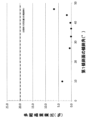
- FIG. 3 is a graph diagram showing the relationship between the inclination angle of the first inclined surface and the weight ratio of generated polycrystals according to an example.
- FIG. 1 is a diagram schematically showing a longitudinal cross section of a base substrate according to an embodiment of the present invention, and particularly a diagram schematically showing a cross section including a central axis O of the base substrate.
- This base substrate is an example of the "aluminum nitride single crystal substrate" according to the present invention.
- the base substrate 1 according to this embodiment functions as a seed substrate serving as a template on which an aluminum nitride single crystal layer is grown.
- the "aluminum nitride single crystal substrate” of the present invention may be any substrate that can be used to grow an aluminum nitride single crystal layer, and is not limited to the base substrate 1.
- the "aluminum nitride single crystal substrate” of the present invention is a laminate in which an aluminum nitride single crystal layer is grown on a base substrate 1, the surface of which is polished to an epi-ready state, or a substrate in which the base substrate 1 is separated from the laminate. (Also referred to as "aluminum nitride single-crystal free-standing substrate.")
- a base substrate 1 As shown in FIG. 1, a base substrate 1 according to an embodiment of the present invention has a main surface on which an aluminum nitride single crystal layer (a crystal layer formed by laminating thin films made of aluminum nitride single crystals) grows. 10, and a back surface 71 located on the opposite side of the main surface 10.
- the base substrate 1 has a substantially disk-like shape when viewed from the top and bottom of FIG. 1 .
- its diameter is not limited to a specific length, but is preferably 32 mm to 211 mm.
- the main surface 10 is not particularly limited in plane orientation as long as it is a surface on which an aluminum nitride crystal layer can be grown; however, in order to improve the quality of the aluminum nitride single crystal layer, the main surface 10 of the base substrate , (0001) plane (+c plane, aluminum polar plane), (10-10) plane (m plane, non-polar plane), or (11-20) plane (a plane, non-polar plane).
- the main surface 10 is a (0001) plane (+c plane, aluminum polar plane)
- the back surface 71 is a (000-1) plane ( ⁇ c plane, nitrogen polar plane).
- the main surface 10 has a substantially flat shape, and is connected to a flat surface 11 extending from the center side to the outer peripheral side of the base substrate 1 at an end 31 of the flat surface 11, It has an inclined surface 12 that is inclined toward the back surface 71 with respect to the flat surface 11.
- the base substrate 1 has an aluminum polar surface as the main surface 10, is connected to the aluminum polar surface at the end of the aluminum polar surface, and is connected to the aluminum polar surface at the end of the aluminum polar surface. and an inclined surface 12 that is inclined in the direction of the back surface 71 located on the opposite side.
- the inclined surface 12 is a surface connected to the flat surface 11 and inclined in the direction of the back surface 71.
- the inclined surface 12 may be a flat surface or a curved surface, and in the case of a curved surface, it may be convex or concave. Further, the inclined surface 12 may be composed of a plurality of surfaces.
- the sloped surface 12 includes a first sloped surface 13 that connects to the flat surface 11, and an end portion of the first sloped surface 13 (of both ends of the first sloped surface 13, the base substrate An end located on the outer circumferential side in the radial direction of the sloping surface.
- It is composed of two surfaces, with two inclined surfaces 14.
- the "slanted surface" of the present invention means the inclined surface connected to the flat surface 11. In the form of FIG. 1, this refers to the first inclined surface 13 that is connected to the flat surface 11.
- the first inclined surface 13 has the shape of a curved surface that is gently curved in a convex shape in the cross-sectional view shown in FIG. It is preferable that the surface of the first inclined surface 13 has a very small damage layer that may be generated by polishing, which will be described later, and has a state close to a mirror surface. Further, the first inclined surface 13 in the form shown in FIG. 1 has an inclined angle 61 with respect to the surface direction of the flat surface 11 (see first virtual plane 51).
- the second inclined surface 14 is a plane having a substantially flat shape.
- the angle of inclination (not shown) of the second inclined surface 14 with respect to the surface direction of the flat surface 11 is larger than the angle of inclination 61 of the first inclined surface 13.
- the inclination angle 61 is 10° or more and 50° or less.
- the ratio of the weight of the polycrystal to the weight of the aluminum nitride single crystal layer grown on the base substrate 1 (hereinafter also simply referred to as "polycrystal weight ratio") is achieved. ) can be suppressed to about 1/3 of the level (about 20%) that can be achieved with conventional technology. It is presumed that by setting the angle within the above range, the inclined surface can easily form a state close to a mirror surface, so that the occurrence of a crown can be suppressed.
- the inclination angle 61 is 10° or more and 45° or less.
- the polycrystalline weight ratio can be suppressed to 5% or less.
- the inclination angle 61 is more preferably 25° or more and 45° or less, still more preferably 25° or more and 40° or less, and even more preferably 30° or more and 40° or less.
- the polycrystalline weight ratio can be further suppressed, and specifically, can be suppressed to 2% or less.
- the polycrystalline weight ratio can be suppressed to 1% or less.
- the polycrystalline weight ratio can be suppressed to 0.5% or less.
- the inclination angle 61 is set to 25° or more and 40° or less (particularly 30° or more and 40° or less), the polycrystal content ratio can be kept small even if the width 15 of the first inclined surface 13 described later is widened. can. That is, by setting the inclination angle 61 to 25° or more and 40° or less (particularly 30° or more and 40° or less), the degree of freedom in design regarding the width 15 can be increased.
- the height 21 of the first inclined surface 13 is preferably 10 ⁇ m or more, more preferably 100 ⁇ m or more, since it is preferable to have a large machining allowance in order to remove the damaged layer. Further, the height 21 of the first inclined surface 13 is preferably 250 ⁇ m or less, more preferably 200 ⁇ m or less, and even more preferably 170 ⁇ m or less. That is, the height 21 of the first inclined surface 13 is preferably 10 ⁇ m or more and 250 ⁇ m or less, more preferably 100 ⁇ m or more and 200 ⁇ m or less, and even more preferably 100 ⁇ m or more and 170 ⁇ m or less.
- the height 21 of the first inclined surface 13 includes the flat surface 11 in the cross section shown in FIG. It refers to the distance between the first virtual plane 51 and the end 32 of the first inclined surface 13, in other words, the length of the normal line drawn from the end 32 of the first inclined surface 13 to the first virtual plane 51. means.
- the width 15 of the first inclined surface 13 is preferably 50 ⁇ m or more and 350 ⁇ m or less, more preferably 100 ⁇ m or more and 300 ⁇ m or less, and 100 ⁇ m or more, since it is preferable to have a large machining allowance in order to remove the damaged layer. It is more preferably 250 ⁇ m or less, and even more preferably 100 ⁇ m or more and 180 ⁇ m or less.
- the "width 15 of the first inclined surface 13" refers to the width 15 from the end 31 of the flat surface 11 in the plan view of the base substrate 1 (when viewed from above in FIG. 1) in the form shown in FIG. In other words, it refers to the distance from the end 31 of the flat surface 11 to the end 32 of the first slope 13 in the radial direction of the base substrate 1 (hereinafter referred to as (Similar explanations may be omitted.)
- the base substrate 1 shown in FIG. 1 is shown as having two inclined surfaces, the first inclined surface 13 and the second inclined surface 14, the number of surfaces constituting the inclined surface 12 is not necessarily two. It is not limited. That is, the base substrate 1 may have one inclined surface or may have three or more inclined surfaces.
- the inclination angle of the one inclined surface satisfies the above range, and the width and height of the one inclined surface each satisfy the above range. preferable.
- the inclination angle of at least the inclined surface closest to the flat surface 11 i.e., the first inclined surface 13
- the at least flat surface it is preferable that the width and height of the inclined surface closest to No. 11 satisfy the above ranges, respectively.
- the area of the main surface 10 of the base substrate 1 is not limited to a specific range, it is preferably 800 mm 2 to 35000 mm 2 .
- the thickness of the base substrate 1 is not limited to a specific range, but may be determined within a range that does not cause cracking due to insufficient strength when growing an aluminum nitride single crystal layer. Specifically, the thickness of the base substrate 1 is preferably 50 ⁇ m to 2000 ⁇ m, more preferably 100 ⁇ m to 1000 ⁇ m.
- the surface roughness (root mean square roughness) is 0.05 nm to 0.5 nm, and the condition is determined by observation using an atomic force microscope or a scanning probe microscope. It is preferable that atomic steps are observed in a field of view of about 2 ⁇ m ⁇ 2 ⁇ m.
- Surface roughness can be adjusted, for example, by chemical mechanical polishing (CMP).
- CMP chemical mechanical polishing
- the surface roughness is measured using, for example, an atomic force microscope or a scanning probe microscope, after removing foreign matter and contaminants from the main surface 10 of the base substrate 1, and measuring the surface roughness by observing a field of view of 5 ⁇ m x 5 ⁇ m. You can ask for it.
- the radius of curvature of the main surface 10 of the base substrate 1 is not particularly limited, but is preferably in the range of 5 m to 10,000 m.
- the radius of curvature of the main surface 10 of the base substrate 1 is more preferably 6 m to 10,000 m, and still more preferably 8 m to 10,000 m.
- the crystal lattice plane forming the main surface 10 of the base substrate 1 or the main surface 10 is not particularly limited, but is preferably in the range of 2 m to 10,000 m.
- the radius of curvature of the crystal lattice plane forming the main surface 10 of the base substrate 1 or the crystal lattice plane parallel to the main surface 10 is small. Therefore, the radius of curvature of the crystal lattice plane is preferably 5 m to 10,000 m, more preferably 10 m to 10,000 m.
- the X-ray omega ( ⁇ ) rocking curve of a specific crystal plane is measured under the condition that the incident angle of X-rays with respect to the main surface 10 is 4 degrees or less. It is preferable that the half width is 200 seconds or less.
- the specific crystal plane is the (10-13) plane
- the specific crystal plane is the (10-16) plane.
- the main surface 10 is the (11-20) plane
- the specific crystal plane is the (114) plane.
- the incident angle of X-rays with respect to the main surface means the angle formed by the main surface 10 and the traveling direction of the X-rays.
- the traveling direction of the X-rays is perpendicular to the main surface 10
- the "incident angle of the X-rays with respect to the main surface” is 90 degrees.
- the main surface 10 of the base substrate made of aluminum nitride single crystal ( Tilt in the m-axis direction within a range of 0.00° or more and 1.00° or less from the (0001) plane, and tilted in the a-axis direction within a range of 0.00° or more and 1.00° or less from the (0001) plane. It is preferable that at least one of the inclination angle of the main surface 10 in the m-axis direction and the inclination angle of the main surface 10 in the a-axis direction is greater than 0.00°.
- the shape of the base substrate 1 is not limited to a substantially circular shape in plan view, but may be an ellipse, a polygon such as a quadrangle or a hexagon, or an amorphous shape. However, since it is easy to uniformly form the inclined surface 12 over the entire circumference of the base substrate 1, it is more preferable that the base substrate 1 is circular in plan view.
- the crystal growth surface on which the aluminum nitride single crystal layer grows may be only the flat surface 11. That is, the "aluminum nitride single crystal substrate" of the present invention does not exclude those in which the aluminum nitride single crystal does not grow from the inclined surface 12.
- This base substrate 1 may be grown by a sublimation method (physical vapor transport method, PVT method) or a hydride vapor phase epitaxy method (HVPE method). good. Furthermore, it may be grown by a liquid phase method, and it is also possible to use a base substrate that has been processed with island-like or stripe-like irregularities in advance. Furthermore, as in Patent Document 1, it is also possible to use it as a recycled base substrate that has been repeatedly subjected to a circulation process.
- a sublimation method physical vapor transport method
- HVPE method hydride vapor phase epitaxy method
- the first inclined surface 13 can be formed by known edge polishing, surface mirror polishing lapping, or chemical mechanical polishing (CMP). By performing the polishing process by rotating both the base substrate 1 and the polishing disk on which the base substrate 1 is mounted, or either one thereof, the shape of the outer edge of the base substrate 1 is approximately changed over the entire circumference. The shape will be the same.
- the second inclined surface 14 (if there are three or more inclined surfaces, the second inclined surface and subsequent inclined surfaces) is formed by a known outer circumferential grinding process in addition to the above-mentioned polishing process.
- the flat surface 11 is formed by the CMP described above.
- the shape of the first inclined surface 13, such as the angle of inclination 61, height 21, width 15, etc., is determined by considering the quality of the flat surface 11, the processing conditions of the edge polishing, mirror polishing lapping, CMP, abrasive, polishing, etc. It can be adjusted by combining the pads. For example, by increasing the load during processing, the base substrate 1 is more likely to sink into the polishing pad, and the outer edge of the base substrate 1 is more likely to come into contact with the polishing pad, so that the inclination angle 6 of the first inclined surface 13 , the height 21 and the width 15 can be respectively increased.
- Commercially available products can be used as the processing equipment, polishing agent, and polishing pad.
- an abrasive containing at least one material selected from the group consisting of silica, alumina, ceria, silicon carbide, boron nitride, and diamond can be used.
- the property of the abrasive may be alkaline, neutral, or acidic.
- aluminum nitride has low alkali resistance on the nitrogen polar plane (-c plane)
- a protective film is formed on the nitrogen polar surface, it is also possible to use a strong alkaline polishing agent without any problem. It is also possible to add additives such as oxidizing agents to the polishing agent in order to increase the polishing rate.
- a commercially available polishing pad can be used, and its material, structure, and hardness are not particularly limited.
- the angle of inclination, width, and height of the inclined surface 12 can be calculated using a known measuring device or calculation.
- the inclination angle 61 of the first inclined surface 13 is a virtual plane (hereinafter also referred to as "second virtual plane") 52 passing through the end 31 of the flat surface 11 and the end 32 of the first inclined surface 13. It can be calculated by a method of measuring the angle (acute angle) formed by the first virtual plane 51 and the above-mentioned first virtual plane 51. Note that such calculation processing can be performed, for example, by analysis using image processing.
- the aluminum nitride single crystal layer grown on the base substrate 1 preferably has a thickness of 500 ⁇ m or more. This ensures that the resulting aluminum nitride single-crystal layer has a sufficient thickness, and that the aluminum nitride single-crystal layer has sufficient strength when processed into wafers for device manufacturing by grinding and polishing. It becomes easier.
- the upper limit of the thickness of the aluminum nitride single crystal layer grown in vapor phase on the base substrate 1 is not particularly limited, but is 2000 ⁇ m in consideration of industrial production. If the aluminum nitride single crystal layer to be grown is excessively thick, it will take time for the growth process and polishing process. Therefore, considering industrial production, the thickness of the aluminum nitride single crystal layer grown in the growth process is 600 ⁇ m. It is preferably from 1,500 ⁇ m to 1,500 ⁇ m, and more preferably from 800 ⁇ m to 1,200 ⁇ m.
- the in-plane thickness difference of the aluminum nitride single crystal layer (this is the height difference between the highest and lowest in-plane positions of the aluminum nitride single crystal layer) is related to the processing time of the growth surface processing process. Therefore, it is preferable to have a smaller thickness difference because the processing time will be shorter.
- the in-plane thickness difference of the aluminum nitride single crystal layer is preferably 5 ⁇ m to 600 ⁇ m, more preferably 5 ⁇ m to 300 ⁇ m.
- the aluminum nitride single crystal layer may be grown by any one of a sublimation method, a liquid phase method, and a vapor phase growth method.
- the aluminum source is the vapor obtained by subliming or decomposing aluminum nitride
- the nitrogen source is the vapor obtained by subliming or decomposing aluminum nitride, or the nitrogen gas supplied to the growth apparatus.
- the aluminum source and the nitrogen source are solutions in which aluminum nitride is dissolved.
- the aluminum source is an aluminum halide gas such as aluminum chloride, aluminum iodide, or aluminum bromide, or an organic aluminum gas such as trimethylaluminum or triethylaluminum
- the nitrogen source is ammonia gas or nitrogen gas. It is.
- the HVPE method has a slower growth rate than the sublimation method, it is suitable for manufacturing substrates made of aluminum nitride single crystals for light emitting devices because it can reduce the concentration of impurities that adversely affect deep ultraviolet light transmittance. Further, since impurities can be reduced, the concentration of point defects such as aluminum vacancies that adversely affect electron mobility is lowered, and therefore it is suitable for manufacturing substrates made of aluminum nitride single crystals for electronic devices.
- the concentration of carbon contained as an impurity in the final aluminum nitride single crystal substrate is easier to suppress to 3 ⁇ 10 17 atoms/cm 3 or less than with other vapor phase growth methods.
- the lower limit of carbon concentration is not particularly limited, but is 1 ⁇ 10 14 atoms/cm 3 .
- the HVPE method has a faster growth rate than the liquid phase method, it is possible to grow a single crystal with good crystallinity at a fast deposition rate, so it is a manufacturing method that balances crystal quality and mass productivity. It is.
- the vapor phase growth apparatus (HVPE apparatus) used in the HVPE method is not particularly limited, and any known apparatus can be employed.
- the aluminum nitride single crystal layer is grown by supplying an aluminum source gas and a nitrogen source gas onto the base substrate 1 and causing both gases to react on the heated base substrate.
- the method for producing an aluminum nitride single crystal layer involves vapor phase growth of an aluminum nitride single crystal layer on the base substrate 1 by supplying an aluminum source gas and a nitrogen source gas onto the base substrate 1 and causing them to react. Including process.
- an aluminum halide gas such as aluminum chloride gas, or a mixed gas of aluminum organometallic gas and hydrogen halide gas is used. Furthermore, ammonia gas is preferably used as the nitrogen source gas.
- a carrier gas such as hydrogen gas, nitrogen gas, argon gas, helium gas, or the like.
- the carrier gas one type of gas may be used alone, or two or more types of gas may be used in combination.
- halogen gas such as halogen gas or hydrogen halide gas may be additionally supplied to the aluminum source gas and nitrogen source gas to suppress the generation of metal aluminum due to disproportionation reaction from the aluminum halide gas. .
- the nozzle shape and reactor shape that supply raw material gas to the base substrate, the composition of the carrier gas, the carrier gas supply amount, the linear velocity of the gas flow in the reactor, the growth pressure (the pressure in the reactor) ), growth-related conditions such as heating temperature (growth temperature) of the base substrate are adjusted as appropriate so that an aluminum nitride single crystal layer of good crystal quality can be obtained at a desired growth rate.
- Typical growth conditions include aluminum source gas of 0.1 sccm to 100 sccm, nitrogen source gas of 1 sccm to 10,000 sccm, additionally supplied halogen gas of 0.1 sccm to 10,000 sccm, carrier gas total flow rate of 1,000 sccm to 100,000 sccm, and carrier gas of 0.1 sccm to 100 sccm.
- Examples of conditions include gas compositions of nitrogen, hydrogen, argon, and helium (the gas composition ratio is arbitrary), a growth pressure of 36 Torr to 1000 Torr, and a base substrate heating temperature (growth temperature) of 1200° C. to 1800° C.
- the aluminum nitride single crystal layer is grown while supplying impurities (for example, compounds containing Si, Mg, S, etc.) that serve as donors and acceptors as appropriate. It is also possible to do so.
- impurities for example, compounds containing Si, Mg, S, etc.
- the average value over time of the ratio of the nitrogen atomic weight to the group III atomic weight (nitrogen atomic weight/group III atomic weight) in the group III source gas and the nitrogen source gas that reach the outer edge is 0.5 to 3. It is more preferable to control it to .0.
- the present invention will be explained with reference to examples, but the present invention is not limited to the following examples.
- the ratio of the weight of polycrystals grown in a convex shape called a crown that occurs at the outer edge to the weight of the aluminum nitride single crystal layer, and the shape of the end face of the base substrate are determined by the following procedure. Measured at Note that the following embodiments will be described without numbering.
- the ratio of the weight of the polycrystal to the weight of the aluminum nitride single crystal was calculated by dividing the weight of the polycrystal by the weight of the aluminum nitride single crystal layer.
- the shape of the inclined surface of the base substrate was measured using a laser microscope (manufactured by Keyence: VK-X3050). A laser beam wavelength of 661 nm was used.
- the base substrate was placed on a stage and measurements were taken. At this time, the objective lens was 50x and the measurement pitch was 0.26 ⁇ m.
- the measurement depth was set to be equal to or greater than the thickness of the base substrate.
- the angle, height, and width of the slope were measured using the attached software (VK-X3000 multi-file analysis application). The angle of the slope was calculated from the measured values of the height and width of the slope.
- the measurement position was an inclined surface located on the opposite side of the center point from the orientation flat of the base substrate.
- the thickness of the aluminum nitride single crystal layer was measured by laser irradiation using a non-contact thickness measuring device manufactured by FA Systems. Note that the thickness of the aluminum nitride single crystal layer may be measured using a micrometer.
- Example 1 (Base board) As a base substrate, an aluminum nitride single crystal having a diameter of 50.8 mm and a thickness of approximately 500 ⁇ m was prepared by CMP polishing using a polishing pad with a hardness of 48° and an opening diameter of 70 ⁇ m. When the inclined surface was observed with a laser microscope, it was found that the inclined surface had only one surface, the first inclined surface. The angle, height, and width of the inclined surface opposite the orientation flat were 44°, 201 ⁇ m, and 210 ⁇ m, respectively. The (11-24) plane and (10-12) plane appeared on the inclined plane.
- a base substrate is placed on a susceptor in an HVPE device equipped with a heating mechanism using high-frequency induction heating, with the aluminum polar surface facing upward, and the heating temperature of the substrate is set to 1500°C, and the pressure inside the reactor is set to 500 Torr.
- a total of 16,650 sccm of aluminum trichloride gas, 250 sccm of ammonia gas, and nitrogen gas and hydrogen gas as carrier gases were flowed to grow an aluminum nitride single crystal layer on the base substrate.
- the growth time was 16 hours, and the thickness of the aluminum nitride single crystal layer at the in-plane center position (hereinafter also referred to as "substrate center position") was 1,141 ⁇ m.
- the polycrystalline weight ratio was 1.7%.
- Example 2 (Base board) As a base substrate, an aluminum nitride single crystal with a diameter of 50.8 mm and a thickness of about 360 ⁇ m was prepared. At this time, processing was carried out in the same manner as in Example 1, except that a polishing pad whose hardness was approximately 30% lower than that used in the CMP of the surface in Example 1 was used. When the inclined surface was observed with a laser microscope, it was found that the inclined surface had only one surface, the first inclined surface. The angle, height, and width of the inclined surface opposite the orientation flat were 40°, 151 ⁇ m, and 178 ⁇ m, respectively. The (11-26) plane and (10-13) plane appeared on the inclined plane.
- An aluminum nitride single crystal layer was grown on a base substrate using the same equipment and growth conditions as in Example 1. The growth time was 16 hours, and the thickness of the aluminum nitride single crystal layer at the center of the substrate was 1,182 ⁇ m. The polycrystalline weight ratio was 0.3%.
- Example 3 (Base board) As a base substrate, an aluminum nitride single crystal with a diameter of 50.8 mm and a thickness of about 330 ⁇ m was prepared. At this time, the same processing as in Example 2 was performed, except that edge polishing was added to the conditions of Example 2 to reduce the damage layer on the outer periphery and CMP was performed on the surface. When the inclined surface was observed with a laser microscope, it was found that the inclined surface had only one surface, the first inclined surface. The angle, height, and width of the slope opposite the orientation flat were 37°, 114 ⁇ m, and 152 ⁇ m, respectively.
- An aluminum nitride single crystal layer was grown on a base substrate using the same equipment and growth conditions as in Example 1. The growth time was 16 hours, and the thickness of the aluminum nitride single crystal layer at the center of the substrate was 1,136 ⁇ m. The polycrystalline weight ratio was 0.0%.
- Example 4 (Base board) As a base substrate, an aluminum nitride single crystal with a diameter of 50.8 mm and a thickness of about 400 ⁇ m was prepared. Processing was carried out in the same manner as in Example 1, except that the polishing pad used in the CMP of the surface of Example 1 was changed to a polishing pad with 20% lower hardness and approximately 30% smaller opening diameter. When the inclined surface was observed with a laser microscope, it was found that the inclined surface had two surfaces, a first inclined surface and a second inclined surface. The angle, height, and width of the first inclined surface opposite the orientation flat were 27°, 113 ⁇ m, and 224 ⁇ m, respectively.
- An aluminum nitride single crystal layer was grown on a base substrate using the same equipment and growth conditions as in Example 1. The growth time was 16 hours, and the thickness of the aluminum nitride single crystal layer at the center of the substrate was 1,142 ⁇ m. The polycrystalline weight ratio was 0.6%.
- Example 5 (Base board) As a base substrate, an aluminum nitride single crystal with a diameter of 50.8 mm and a thickness of about 370 ⁇ m was prepared. At this time, processing was performed in the same manner as in Example 2, except that the surface plate rotation speed was increased by 25% from the surface CMP processing conditions of Example 2. When the inclined surface was observed with a laser microscope, it was found that the inclined surface had only one surface, the first inclined surface. The angle, height and width of the slope opposite the orientation flat were 33°, 212 ⁇ m and 321 ⁇ m, respectively. The (11-25) plane and (20-25) plane appeared on the inclined plane.
- An aluminum nitride single crystal layer was grown on a base substrate using the same equipment and growth conditions as in Example 1. The growth time was 16 hours, and the thickness of the aluminum nitride single crystal layer at the center of the substrate was 1,053 ⁇ m. The polycrystalline weight ratio was 0.0%.
- Example 6 (Base board) As a base substrate, a recycled base substrate that had been subjected to the circulation process described in the example of Patent Document 1 once was prepared, and an aluminum nitride single crystal having a diameter of 50.8 mm and a thickness of about 360 ⁇ m was prepared. At this time, processing was carried out in the same manner as in Example 1, except that the polishing pad used in the CMP of the surface of Example 1 was changed to a polishing pad with an opening diameter approximately 40% smaller. When the inclined surface was observed with a laser microscope, it was found that the inclined surface had only one surface, the first inclined surface. The angle, height and width of the slope opposite the orientation flat were 10°, 14 ⁇ m and 82 ⁇ m, respectively.
- An aluminum nitride single crystal layer was grown on a base substrate using the same equipment and growth conditions as in Example 1. The growth time was 16 hours, and the thickness of the aluminum nitride single crystal layer at the center of the substrate was 1,129 ⁇ m. The polycrystalline weight ratio was 3.5%.
- Example 7 (Base board) As a base substrate, an aluminum nitride single crystal with a diameter of 50.8 mm and a thickness of about 480 ⁇ m was prepared. At this time, processing was carried out in the same manner as in Example 1, except that the polishing pad used in the CMP of the surface of Example 1 was changed to a polishing pad with a compressibility lowered by about 40%. When the inclined surface was observed with a laser microscope, it was found that the inclined surface had only one surface, the first inclined surface. The angle, height and width of the slope opposite the orientation flat were 47°, 94 ⁇ m and 87 ⁇ m, respectively.
- An aluminum nitride single crystal layer was grown on a base substrate using the same equipment and growth conditions as in Example 1. The growth time was 16 hours, and the thickness of the aluminum nitride single crystal layer at the center of the substrate was 1,185 ⁇ m. The polycrystalline weight ratio was 6.7%.
- Example 6 described in Patent Document 2 is given. It is known that the occurrence of crown tends to become more pronounced as the thickness of the aluminum nitride single crystal layer grown on the base substrate increases. Therefore, as a comparative example, an example having a large thickness was selected from among the examples described in Patent Document 2.
- Patent Document 2 lists examples in which the thickness of the aluminum nitride single crystal layer at the center position of the substrate is 100 to 140 ⁇ m and 800 to 840 ⁇ m. Of the latter three examples (specifically, Examples 6 to 8) having a thickness of 800 to 840 ⁇ m, the “crown mass increase ratio” that can correspond to the above “polycrystal weight ratio” is the most Example 6, which is suppressed, was selected as a comparative example in this paper.
- Example 6 uses a base substrate that has an inclined surface with a width of 0.2 mm (ie, width of 200 ⁇ m) at the outer edge by chamfering the edges before CMP.
- a width of 0.2 mm ie, width of 200 ⁇ m
- the "crown mass increase ratio" in Example 6 is 0.20 (ie, 20%).
- FIG. 2 summarizes the relationship between the inclination angle of the first inclined surface and the polycrystal weight ratio according to Examples 1 to 7.
- the horizontal axis in FIG. 2 indicates the inclination angle (°) of the first inclined surface
- the vertical axis indicates the polycrystalline weight ratio.
- the polycrystalline weight ratio is expressed as a ratio to the aluminum nitride single crystal layer.
- the horizontally long thick broken line in FIG. 2 indicates the polycrystalline weight ratio (20%) in the comparative example.
- the structure according to the present invention maximizes the polycrystalline weight ratio even under conditions where the aluminum nitride single crystal film thickness is 800 ⁇ m or more at the center of the substrate, where crown growth is likely to occur. However, it becomes possible to reduce the amount to 6.7% or less, and by adjusting the conditions, it becomes possible to further suppress the polycrystalline weight ratio and bring the occurrence of crowns as close to zero as possible.
- Examples 1 to 5 are more effective in that the "polycrystal weight ratio" can be made smaller. Moreover, among Examples 1 to 5, Examples 2 to 5 are more effective in that the "polycrystal weight ratio" can be further reduced, specifically, 1% or less.
- the inclination angle of the first inclined surface is more preferably 25° or more and 40° or less, and optimally 30° or more and 40° or less.
- the inclination angle is set to 30° or more and 40° or less, even if the width of the first inclined surface is increased to 300 ⁇ m or more, the polycrystalline weight ratio can be reduced to 0.5%. It can be kept within. That is, as shown from a comparison between Examples 2 and 3 and Example 5, by setting the inclination angle to 30° or more and 40° or less, the degree of freedom in design regarding width can be increased.
- Base substrate 10 Main surface 11 on which thin films are laminated Flat surface 12 Inclined surface 13 First inclined surface 14 Second inclined surface 15 Width of first inclined surface 21 Height of first inclined surface 31 End portion of flat surface 32 First End portion of the inclined surface 51 First virtual plane 52 Second virtual plane 61 Inclination angle of the first inclined surface 71 Back surface O Central axis
Landscapes
- Chemical & Material Sciences (AREA)
- Inorganic Chemistry (AREA)
- Engineering & Computer Science (AREA)
- Materials Engineering (AREA)
- Metallurgy (AREA)
- Organic Chemistry (AREA)
- Crystallography & Structural Chemistry (AREA)
- General Chemical & Material Sciences (AREA)
- Chemical Kinetics & Catalysis (AREA)
- Mechanical Engineering (AREA)
- Crystals, And After-Treatments Of Crystals (AREA)
Abstract
【課題】窒化アルミニウム単結晶層の端部又は外縁部に発生する凸状に成長したクラウンと呼ばれる多結晶を抑制することができるベース基板、及びかかるベース基板を用いて該ベース基板上に窒化アルミニウム単結晶層を成長させることを含む窒化アルミニウム単結晶基板の製造方法を提供する。 【解決手段】窒化アルミニウム単結晶層を成長させる主面を有する窒化アルミニウム単結晶基板であって、主面は、該ベース基板の中心側から外周側に延在する平坦面と、該平坦面の端部において平坦面と接続し、該平坦面に対して該平坦面の反対側に位置する裏面の方向に傾斜する傾斜面と、を備え、平坦面の面方向に対する傾斜面の傾斜角は、10°以上50°以下である、窒化アルミニウム単結晶基板。
Description
本発明は、窒化アルミニウム単結晶基板、特に、窒化アルミニウム単結晶層を成長させるベース基板として用いられる窒化アルミニウム単結晶基板、および、その製造方法に関する。
従来、ベース基板上の表面上に窒化アルミニウム単結晶(以下、「AlN単結晶」ともいう。)層を成長させてAlN単結晶基板を製造する方法が知られている(例えば、特許文献1参照。)。
特許文献1には、AlN単結晶からなるベース基板の主面上にAlN単結晶層を成長した後、該ベース基板とAlN単結晶層とを分離して、AlN単結晶基板を製造する方法が開示されている。このAlN単結晶基板の製造方法は、前記ベース基板と該ベース基板の主面上に成長された前記AlN単結晶層とを有する積層体を得る成長工程、前記積層体の前記AlN単結晶層部分を切断することにより、前記積層体をAlN単結晶層の少なくとも一部の薄膜が積層したベース基板とそれ以外のAlN単結晶層部分とに分離する分離工程、該薄膜が積層したベース基板の薄膜の表面を研磨する再生研磨工程、及び該再生研磨工程で得られたAlN単結晶からなる再生ベース基板を、その研磨した表面上にAlN単結晶を成長させるベース基板として使用する循環工程を含むことを特徴とする。
ところで、ベース基板上の表面上にAlN単結晶層を成長させる時、AlN単結晶層の端部又は外縁部に凸状に成長したクラウンとよばれる多結晶が形成される場合があることが知られている。このクラウンは、成長させる単結晶層の膜厚が大きくなるほど顕著となる。クラウンとその付近の領域は、他の領域と比較して、結晶品質が悪く、半導体素子製造用基板として使用することに適さない。ベース基板の表面を研磨しエピレディの状態に仕上げる場合、このクラウンを除去する必要があり、これによりベース基板の直径を小さくしてしまうという問題がある。
特に、特許文献1に記載されているAlN単結晶のベース基板を繰り返し使用する方法によれば、ベース基板の表面上にAlN単結晶層を成長させるときにクラウンが発生してしまう場合、繰り返し使用するための再生ベース基板を作製する際に前記の循環工程を繰り返すたびにクラウンを除去する必要が生じることから、前記の問題が特に顕著となる。
これに対して、特許文献1には、AlN単結晶層の外周に発生した多結晶を除去する目的として外周研削工程を導入する方法が開示されている。しかしながら、ベース基板を繰り返し使用する度に当該方法を適用し続けると、再生ベース基板の厚さが薄くなったり直径が小さくなってしまう虞がある。
かかる状況を鑑み、従来、クラウンの発生を抑制する方法が提案されてきた。例えば、引用文献2では、表面がCMPされた直径25mmの円形のベース基板や7mm四方である正方形形状のベース基板を準備し、該ベース基板におけるIII族窒化物単結晶層を成長させる面が(0001)面であり、前記のIII族窒化物単結晶層を成長させる面の外縁部上に到達するIII族源ガスと窒素源ガスにおけるIII族原子量に対する窒素原子量の比(窒素原子量/III族原子量)の経時平均値を0.5~3.0に制御することによりクラウンの発生を抑制する方法が提案されている。
また、引用文献3では、(000-1)面を所定の方向に傾斜させた面である表面と、傾斜面を有する側面とを備えるGaNからなるベース基板の表面及び側面上にGaN単結晶からなる半導体を成長させる成長工程を有し、この成長させたGaN単結晶からなる半導体の上面の面積が、ベース基板の表面の面積よりも大きくなるようにGaN単結晶からなる半導体を成長させる方法が提案されている。
Phys.Status Solidi C 6, No.S2(2009)
しかしながら、特許文献2に記載の方法によれば、ベース基板が大きくなればIII族原子量に対する窒素原子量の比を制御する範囲が増大し、該比の制御が困難になる虞があることから、当該方法は、必ずしも直径25mmよりも大きなベース基板に適している方法とはいえない。また、当該方法を直径25mmよりも大きな基板に適用する際の対策として成長装置を大型化する方法もあるが、その場合、温度勾配も大きくなり、緻密な制御が要求される。加えて、原料を増加し生産性を向上させる場合、より高度な制御が要求される。
また、引用文献2に記載の方法によれば、ベース基板の径が比較的小さいことから、ベース基板の寸法よりも大きな径を有するサセプタを用いており、これによりベース基板をサセプタの中心から所定の距離を離した位置に設置する(すなわち、オフセットする)ことによって原料の濃度比の調整を図っている。しかしながら、成長の対象とする窒化アルミニウム単結晶層の径が大きくなりサセプタとベース基板との間に一定の余裕が得られない場合、オフセットした場合とは異なる原料消費のため、原料比のばらつきが生じやすい。
かかる点において、特許文献2に記載の方法は、特に大口径化された窒化アルミニウム単結晶基板に適用する際にクラウンの発生を抑制する点において改善の余地がある。
また、特許文献3に記載の方法によれば、ベース基板の結晶成長面を(000-1)面として用いているため、かかる方法を窒化アルミニウム単結晶からなるベース基板に適用すると即座に極性反転して(0001)面が成長する虞がある(非特許文献1参照)。上記の極性反転領域は、転位密度が高いため、ベース基板の端部において露出した極性反転領域を起点として却って多結晶を発生させてしまう可能性がある。
また、上述した特許文献3には、成長時のガスの流れの乱れを抑制するという観点から、ベース基板の縁部に傾斜面を有する構成が開示されている。しかしながら、特許文献3に記載の傾斜面は、結晶面か否かは不明であり、また、該傾斜面の角度や高さは、記載されておらず、どのような形状の斜面が適しているかについて明記はされていない。
以上を鑑み、本発明の目的は、窒化アルミニウム単結晶層の端部又は外縁部に発生する凸状に成長したクラウンと呼ばれる多結晶を抑制することができるベース基板、及びかかるベース基板を用いて該ベース基板上に窒化アルミニウム単結晶層を成長させることを含む窒化アルミニウム単結晶基板の製造方法を提供することにある。
本発明者らは、窒化アルミニウム単結晶層の端部又は外縁部にクラウンが発生するベース基板に着目し、上記のクラウンの発生を抑制する方法について、鋭意検討を行った。その結果、ベース基板の外縁部の形状が上記のクラウンの発生を抑制することを見出し、以下の本発明を完成するに至った。
[1] 窒化アルミニウム単結晶層を成長させる主面を有する窒化アルミニウム単結晶基板であって、
前記主面は、該ベース基板の中心側から外周側に延在する平坦面と、該平坦面の端部において前記平坦面と接続し、該平坦面に対して該平坦面の反対側に位置する裏面の方向に傾斜する傾斜面と、を備え、
前記平坦面の面方向に対する前記傾斜面の傾斜角は、10°以上50°以下である、
窒化アルミニウム単結晶基板。
前記主面は、該ベース基板の中心側から外周側に延在する平坦面と、該平坦面の端部において前記平坦面と接続し、該平坦面に対して該平坦面の反対側に位置する裏面の方向に傾斜する傾斜面と、を備え、
前記平坦面の面方向に対する前記傾斜面の傾斜角は、10°以上50°以下である、
窒化アルミニウム単結晶基板。
[2] 前記傾斜面の高さは、10μm以上250μm以下である、[1]に記載の窒化アルミニウム単結晶基板。
[3] 前記窒化アルミニウム単結晶基板の径方向における前記傾斜面の幅は、50μm以上350μm以下である、[1]又は[2]に記載の窒化アルミニウム単結晶基板。
[3] 前記窒化アルミニウム単結晶基板の径方向における前記傾斜面の幅は、50μm以上350μm以下である、[1]又は[2]に記載の窒化アルミニウム単結晶基板。
[4] 前記平坦面は、アルミニウム極性面であり、前記裏面は、窒素極性面である、[1]乃至[3]のいずれか1項に記載の窒化アルミニウム単結晶基板。
[5] 前記傾斜角は、25°以上45°以下である、[1]乃至[4]のいずれか1項に記載の窒化アルミウム単結晶基板。
[5] 前記傾斜角は、25°以上45°以下である、[1]乃至[4]のいずれか1項に記載の窒化アルミウム単結晶基板。
[6] 前記傾斜角は、さらに40°以下である、[5]に記載の窒化アルミニウム単結晶基板。
[7] [1]乃至[6]のいずれか1項に記載の窒化アルミニウム単結晶基板をベース基板とし、該ベース基板上にアルミニウム源ガスと窒素源ガスとを供給して反応させることにより前記ベース基板上に窒化アルミニウム単結晶層を気相成長させる成長工程を含む窒化アルミニウム単結晶の製造方法。
[7] [1]乃至[6]のいずれか1項に記載の窒化アルミニウム単結晶基板をベース基板とし、該ベース基板上にアルミニウム源ガスと窒素源ガスとを供給して反応させることにより前記ベース基板上に窒化アルミニウム単結晶層を気相成長させる成長工程を含む窒化アルミニウム単結晶の製造方法。
本発明によれば、窒化アルミニウム単結晶層の端部又は外縁部に、凸状に成長したクラウンと呼ばれる多結晶が発生することを抑制することができる。それにより、ベース基板の表面を研磨しエピレディの状態に仕上げる場合や、ベース基板を繰り返し使用する場合であっても、他の領域と比較して、結晶品質が悪くなることを抑制して窒化アルミニウム単結晶層を製造することが可能となる。
以下、図面を参照しつつ、本発明の実施の形態について説明する。ただし、本発明はこれらの形態に限定されるものではない。なお、図面は、必ずしも正確な寸法を反映したものではない。また、本明細書においては特に断らない限り、数値A及びBについて「A~B」という表記は「A以上B以下」を意味するものとする。かかる表記において数値Bのみに単位を付した場合には、該当単位が数値Aにも適用されるものとする。また「又は」及び「若しくは」の語は、特に断りのない限り論理和を意味するものとする。
[ベース基板]
図1は、本発明の一実施形態に係るベース基板の縦断面を模式的に示す図であり、特にベース基板の中心軸Oを含む断面を模式的に示す図である。このベース基板は、本発明に係る「窒化アルミニウム単結晶基板」の一例である。本実施の形態に係るベース基板1は、その上に窒化アルミニウム単結晶層を成長させるテンプレートとなる種基板として機能するものである。
図1は、本発明の一実施形態に係るベース基板の縦断面を模式的に示す図であり、特にベース基板の中心軸Oを含む断面を模式的に示す図である。このベース基板は、本発明に係る「窒化アルミニウム単結晶基板」の一例である。本実施の形態に係るベース基板1は、その上に窒化アルミニウム単結晶層を成長させるテンプレートとなる種基板として機能するものである。
なお、本発明の「窒化アルミニウム単結晶基板」は、窒化アルミニウム単結晶層を成長させるために用いることができる基板であればよく、ベース基板1に限定されるものではない。本発明の「窒化アルミニウム単結晶基板」は、ベース基板1に窒化アルミニウム単結晶層を成長させた積層体の表面をエピレディ状態に研磨したものや、前記の積層体からベース基板1を分離した基板(所謂、「窒化アルミニウム単結晶自立基板」ともいう。)を含む。
〔ベース基板の外形〕
図1に示すように、本発明の一実施形態に係るベース基板1は、窒化アルミニウム単結晶層(窒化アルミニウム単結晶からなる薄膜を積層させて形成した結晶層をいう。)が成長する主面10と、この主面10の反対側に位置する裏面71と、を備える。本実施の形態では、ベース基板1は、図1の上下方向から見た形状が略円板状の形状を有している。
円板状のベース基板の場合、その直径は、特定の長さに限定されるものではないが、32mm~211mmであることが好ましい。
図1に示すように、本発明の一実施形態に係るベース基板1は、窒化アルミニウム単結晶層(窒化アルミニウム単結晶からなる薄膜を積層させて形成した結晶層をいう。)が成長する主面10と、この主面10の反対側に位置する裏面71と、を備える。本実施の形態では、ベース基板1は、図1の上下方向から見た形状が略円板状の形状を有している。
円板状のベース基板の場合、その直径は、特定の長さに限定されるものではないが、32mm~211mmであることが好ましい。
主面10は、窒化アルミニウム結晶層を成長できる面であれば特に面方位が限定されるものではないが、窒化アルミニウム単結晶層の品質を向上させるためには、ベース基板1の主面10は、(0001)面(+c面、アルミニウム極性面)、(10-10)面(m面、非極性面)、又は(11-20)面(a面、非極性面)であることが好ましい。本願発明の好ましい形態では、主面10は、(0001)面(+c面、アルミニウム極性面)であり、裏面71は、(000-1)面(-c面、窒素極性面)である。
また、主面10は、略平坦な形状を有し、ベース基板1の中心側から外周側に延在する平坦面11と、この平坦面11の端部31において該平坦面11と接続し、該平坦面11に対して裏面71の方向に傾斜する傾斜面12と、を有している。
すなわち、本実施の形態に係るベース基板1は、主面10としてのアルミニウム極性面と、このアルミニウム極性面の端部において該アルミニウム極性面と接続し、該アルミニウム極性面に対して該アルミニウム極性面の反対側に位置する裏面71の方向に傾斜する傾斜面12と、を備える。
〔傾斜面12〕
傾斜面12は、平坦面11と接続し、裏面71の方向に傾斜する面である。傾斜面12は、平坦な面であってもよく、曲面であってもよく、曲面の場合は、凸状でも凹状でもよい。また、傾斜面12は、複数の面から構成されているものであってもよい。
傾斜面12は、平坦面11と接続し、裏面71の方向に傾斜する面である。傾斜面12は、平坦な面であってもよく、曲面であってもよく、曲面の場合は、凸状でも凹状でもよい。また、傾斜面12は、複数の面から構成されているものであってもよい。
図1に示した形態では、傾斜面12は、平坦面11と接続する第1傾斜面13と、この第1傾斜面13の端部(第1傾斜面13の両端部のうち、ベース基板1の径方向における外周側に位置する端部をいう。以下、傾斜面に係る「端部」についての同様の説明は、省略する場合がある。)32において該第1傾斜面13と接続する第2傾斜面14と、を備えた、2つの面から構成されている。本発明において、本発明の窒化アルミニウム単結晶基板が複数の傾斜面を有している場合、本発明の「傾斜面」とは、平坦面11と接続している傾斜面を意味する。図1の形態では、平坦面11と接続している第1傾斜面13を意味する。
図1に示した形態では、第1傾斜面13は、図1に示す断面視において緩やかに凸状に湾曲する曲面の形状を有している。第1傾斜面13の表面は、後述する研磨加工により発生し得るダメージ層が非常に小さく、鏡面に近い状態であることが好ましい。また、図1に示した形態の第1傾斜面13は、平坦面11の面方向(第1仮想平面51参照。)に対して傾斜角61を有している。
図1に示した形態において、第2傾斜面14は、略平坦な形状を有する平面である。平坦面11の面方向に対する第2傾斜面14の傾斜角(不図示)は、第1傾斜面13の傾斜角61よりも大きい。
(傾斜角61)
傾斜角61は、10°以上50°以下である。傾斜角61を10°以上50°以下とすることによって、ベース基板1上に成長させた窒化アルミニウム単結晶層の重量に対する多結晶の重量の比(以下、単に「多結晶重量比」ともいう。)を、従来技術で達成可能な水準(20%程度)と比較して、約1/3程度まで抑制することができる。前記の角度の範囲にすることで、傾斜面が鏡面に近い状態を形成しやすくなるので、クラウンの発生を抑制することができると推定される。
傾斜角61は、10°以上50°以下である。傾斜角61を10°以上50°以下とすることによって、ベース基板1上に成長させた窒化アルミニウム単結晶層の重量に対する多結晶の重量の比(以下、単に「多結晶重量比」ともいう。)を、従来技術で達成可能な水準(20%程度)と比較して、約1/3程度まで抑制することができる。前記の角度の範囲にすることで、傾斜面が鏡面に近い状態を形成しやすくなるので、クラウンの発生を抑制することができると推定される。
好ましくは、傾斜角61は、10°以上45°以下である。傾斜角61を10°以上45°以下とすることによって、多結晶重量比を5%以下まで抑制することができる。
また、より好ましくは、傾斜角61は、25°以上45°以下であり、さらに好ましくは、25°以上40°以下であり、さらにより好ましくは、30°以上40°以下である。傾斜角61を25°以上45°以下とすることによって、多結晶重量比をさらに抑制することができ、具体的には、2%以下に抑制することができる。また、傾斜角61を25°以上40°以下にすることによって、多結晶重量比を1%以下に抑制することができる。さらに、傾斜角61を30°以上40°以下にすることによって、多結晶重量比を0.5%以下に抑制することができる。また、傾斜角61を25°以上40°以下(とりわけ、30°以上40°以下)にすれば、後述する第1傾斜面13の幅15を広くしたとしても多結晶量比を小さく抑えることができる。すなわち、傾斜角61を25°以上40°以下(とりわけ、30°以上40°以下)にすることにより、幅15に係る設計の自由度を高めることができる。
(高さ21)
第1傾斜面13の高さ21は、ダメージ層を除去するために、取り代が多いことが好ましいため、10μm以上であることが好ましく、100μm以上であることがより好ましい。また、第1傾斜面13の高さ21は、250μm以下であることが好ましく、200μm以下であることがより好ましく、170μm以下であることがさらに好ましい。すなわち、第1傾斜面13の高さ21は、10μm以上250μm以下であることが好ましく、100μm以上200μm以下であることがより好ましく、100μm以上170μm以下であることがさらに好ましい。
第1傾斜面13の高さ21は、ダメージ層を除去するために、取り代が多いことが好ましいため、10μm以上であることが好ましく、100μm以上であることがより好ましい。また、第1傾斜面13の高さ21は、250μm以下であることが好ましく、200μm以下であることがより好ましく、170μm以下であることがさらに好ましい。すなわち、第1傾斜面13の高さ21は、10μm以上250μm以下であることが好ましく、100μm以上200μm以下であることがより好ましく、100μm以上170μm以下であることがさらに好ましい。
図1示す形態において、第1傾斜面13の高さ21は、図1に示す断面(すなわち、平坦面11に直交しベース基板1の中心軸Oを含む断面)視における、平坦面11を含む第1仮想平面51と第1傾斜面13の端部32との距離をいい、換言すれば、第1傾斜面13の端部32から前記の第1仮想平面51に下した法線の長さをいう。
(幅15)
第1傾斜面13の幅15は、ダメージ層を除去するために、取り代が多いことが好ましいため、50μm以上350μm以下であることが好ましく、100μm以上300μm以下であることがより好ましく、100μm以上250μm以下であることがさらに好ましく、100μm以上180μm以下であることがさらにより好ましい。
第1傾斜面13の幅15は、ダメージ層を除去するために、取り代が多いことが好ましいため、50μm以上350μm以下であることが好ましく、100μm以上300μm以下であることがより好ましく、100μm以上250μm以下であることがさらに好ましく、100μm以上180μm以下であることがさらにより好ましい。
ここで、「第1傾斜面13の幅15」とは、図1に示す形態において、ベース基板1の平面視(図1の上方向から見た場合)における平坦面11の端部31から第1傾斜面13の端部32までの距離をいい、言い換えれば、ベース基板1の径方向における、平坦面11の端部31から第1傾斜面13の端部32までの距離をいう(以下、同様の説明は、省略する場合がある。)。
(傾斜面の数)
図1に示すベース基板1として、第1傾斜面13及び第2傾斜面14の2つの傾斜面を有する形態を一例として示したが、傾斜面12を構成する面の数は、必ずしも2つに限られるものではない。すなわち、ベース基板1は、1つの傾斜面を有するものでもよく、3つ以上の傾斜面を有するものでもよい。
図1に示すベース基板1として、第1傾斜面13及び第2傾斜面14の2つの傾斜面を有する形態を一例として示したが、傾斜面12を構成する面の数は、必ずしも2つに限られるものではない。すなわち、ベース基板1は、1つの傾斜面を有するものでもよく、3つ以上の傾斜面を有するものでもよい。
傾斜面が1つである構成の場合、当該1つの傾斜面に係る傾斜角が上記の範囲を満足すればよく、該1つの傾斜面の幅及び高さがそれぞれ上記の範囲を満足することが好ましい。また、傾斜面が3つ以上である構成の場合、少なくとも平坦面11に最も近い傾斜面(すなわち、第1傾斜面13)に係る傾斜角が上記の範囲を満足すればよく、該少なくとも平坦面11に最も近い傾斜面の幅及び高さが上記の範囲をそれぞれ上記の範囲を満足することが好ましい。
〔その他の条件〕
ベース基板1の主面10の面積は、特定の範囲に限定されるものではないが、800mm2~35000mm2であることが好ましい。また、ベース基板1の厚みは、特定の範囲に限定されるものではないが、窒化アルミニウム単結晶層を成長する上で強度不足で割れることのない範囲で決定すればよい。具体的には、ベース基板1の厚みは、50μm~2000μmであることが好ましく、100μm~1000μmであることがより好ましい。
ベース基板1の主面10の面積は、特定の範囲に限定されるものではないが、800mm2~35000mm2であることが好ましい。また、ベース基板1の厚みは、特定の範囲に限定されるものではないが、窒化アルミニウム単結晶層を成長する上で強度不足で割れることのない範囲で決定すればよい。具体的には、ベース基板1の厚みは、50μm~2000μmであることが好ましく、100μm~1000μmであることがより好ましい。
ベース基板1の主面10の状態は、特に制限されるものではないが、表面粗さ(二乗平均粗さ)が0.05nm~0.5nmであり、原子間力顕微鏡や走査プローブ顕微鏡観察により2μm×2μm視野程度で原子ステップが観察されることが好ましい。表面粗さは、例えば、化学的機械的研磨(CMP)で調整することができる。表面粗さの測定は、例えば、原子間力顕微鏡や走査プローブ顕微鏡を用い、ベース基板1の主面10の異物や汚染物を除去した上で行い、5μm×5μm視野の観察から表面粗さを求めることができる。ただし、島状やストライプ状の凹凸加工を主面に施したベース基板1を用いることも可能である。
ベース基板1の主面10の曲率半径は、特に制限されるものではないが、5m~10000mの範囲であることが好ましい。ベース基板1の主面10の曲率半径は、より好ましくは、6m~10000mであり、さらに好ましくは、8m~10000mである。また、ベース基板1の主面10が(0001)面、(11-20)面、又は(10-10)面である場合、ベース基板1の主面10をなす結晶格子面又は主面10に平行な結晶格子面の曲率半径は、特に制限されるものではないが、2m~10000mの範囲であることが好ましい。窒化アルミニウム単結晶層を500μm以上厚く成長させる場合、ベース基板1の主面10をなす結晶格子面又は主面10に平行な結晶格子面の曲率半径が小さいと成長時にクラックが生じることがある。このため、該結晶格子面の曲率半径は好ましくは5m~10000m、さらに好ましくは10m~10000mである。
ベース基板1を構成するAlN単結晶の結晶品質については、前記主面10に対するX線の入射角度が4°以下である条件下で測定される、特定結晶面のX線オメガ(ω)ロッキングカーブ半値幅が200秒以下であることが好ましい。ここで、主面10が(0001)面であるとき、特定結晶面は(10-13)面であり、主面10が(10-10)面であるとき、特定結晶面は(10-16)面であり、主面10が(11-20)面であるとき、特定結晶面は(114)面である。なお、本明細書において、「主面に対するX線の入射角度」とは、主面10とX線の進行方向とがなす角度を意味する。例えば、X線の進行方向が主面10に対して垂直であるとき、「主面に対するX線の入射角度」は90°である。なお、上記特定結晶面のX線オメガロッキングカーブの測定においては、ゲルマニウム単結晶の(220)面で2回回折することにより単色化したX線源を用いることが好ましい。
ベース基板1上に成長させる窒化アルミニウム単結晶層の用途を広げ、かつ得られる窒化アルミニウム単結晶層の厚みをより厚くするためには、窒化アルミニウム単結晶からなるベース基板の主面10が、(0001)面から0.00°以上1.00°以下の範囲でm軸方向に傾斜し、かつ(0001)面から0.00°以上1.00°以下の範囲でa軸方向に傾斜している(0001)面であり、主面10のm軸方向への傾斜角及び前記主面10のa軸方向への傾斜角のうち少なくとも一方は0.00°超であることが好ましい。
〔形状例〕
ベース基板1の形状は、平面視で略円形のものに限定されるものではなく、楕円形、四角形や六角形等の多角形、又は不定形でもよい。但し、ベース基板1の全周に亘って均一に傾斜面12を形成しやすいため、ベース基板1としては、平面視で円形のものがより好ましい。
ベース基板1の形状は、平面視で略円形のものに限定されるものではなく、楕円形、四角形や六角形等の多角形、又は不定形でもよい。但し、ベース基板1の全周に亘って均一に傾斜面12を形成しやすいため、ベース基板1としては、平面視で円形のものがより好ましい。
また、窒化アルミニウム単結晶層が成長する結晶成長面は、平坦面11のみであってもよい。すなわち、本発明の「窒化アルミニウム単結晶基板」は、傾斜面12から窒化アルミニウム単結晶が成長しないものを除外するものではない。
[ベース基板の製造方法]
このベース基板1は、昇華法(physical vapor transport法、PVT法)で成長されたものであっても、ハイドライド気相成長法(Hydride Vapor Phase Epitaxy法、HVPE法)で成長したものであってもよい。また、液相法で成長されたものであってもよく、島状やストライプ状の凹凸加工を事前に行ったベース基板の使用も可能である。さらに、特許文献1のように、循環工程を繰り返し行った再生ベース基板としての使用も可能である。
このベース基板1は、昇華法(physical vapor transport法、PVT法)で成長されたものであっても、ハイドライド気相成長法(Hydride Vapor Phase Epitaxy法、HVPE法)で成長したものであってもよい。また、液相法で成長されたものであってもよく、島状やストライプ状の凹凸加工を事前に行ったベース基板の使用も可能である。さらに、特許文献1のように、循環工程を繰り返し行った再生ベース基板としての使用も可能である。
〔傾斜面の製造方法〕
第1傾斜面13は、公知のエッジ研磨加工、表面の鏡面研磨ラッピング加工や化学的機械的研磨(CMP)で形成することができる。前記研磨加工を、ベース基板1、及び該ベース基板1を載せた研磨盤の両方、又はいずれか一方を自転させて行うことにより、ベース基板1の外縁部の形状は、全周に亘って略同一の形状となる。第2傾斜面14(傾斜面が3つ以上ある場合は第2傾斜面以降の傾斜面)は、前記研磨加工以外に、公知の外周研削加工も含めて形成される。平坦面11は、前記のCMPで形成される。
第1傾斜面13は、公知のエッジ研磨加工、表面の鏡面研磨ラッピング加工や化学的機械的研磨(CMP)で形成することができる。前記研磨加工を、ベース基板1、及び該ベース基板1を載せた研磨盤の両方、又はいずれか一方を自転させて行うことにより、ベース基板1の外縁部の形状は、全周に亘って略同一の形状となる。第2傾斜面14(傾斜面が3つ以上ある場合は第2傾斜面以降の傾斜面)は、前記研磨加工以外に、公知の外周研削加工も含めて形成される。平坦面11は、前記のCMPで形成される。
第一傾斜面13の傾斜角61、高さ21、幅15等の形状は、平坦面11の品質も考慮しつつ、前記エッジ研磨加工や鏡面研磨ラッピング加工、CMPの加工条件、研磨剤、研磨パットの組み合わせにより調整することが出来る。例えば、加工時の荷重を大きくすることで、ベース基板1が研磨パッドに沈み込みやすくなり、ベース基板1の外縁部が研磨パットに接触しやすくなることで、第一傾斜面13の傾斜角61、高さ21及び幅15をそれぞれ大きくすることができる。加工装置、研磨剤、研磨パッドは、市販の製品を適用することができる。
研磨剤としては、シリカ、アルミナ、セリア、炭化ケイ素、窒化ホウ素、ダイヤモンドからなる群より選ばれる少なくとも1つ以上の材質を含む研磨剤を用いることができる。また、研磨剤の性状は、アルカリ性、中性、又は酸性のいずれでもよい。ただし、窒化アルミニウムは、窒素極性面(-c面)の耐アルカリ性が低いため、強アルカリ性の研磨剤よりも、弱アルカリ性、中性又は酸性の研磨剤、具体的には、pH9以下の研磨剤を用いることが好ましい。もちろん、窒素極性面に保護膜を形成すれば強アルカリ性の研磨剤も問題なく使用することも可能である。また、研磨速度を高めるために酸化剤等の添加剤を研磨剤に配合することも可能である。
研磨パットとしては、市販のものを使用することができ、その材質、構造及び硬度は、特に制限されない。
〔傾斜面12の測定方法〕
傾斜面12に係る傾斜角、幅及び高さは、公知の測定装置や計算により算出することができる。例えば、第1傾斜面13の傾斜角61は、平坦面11の端部31及び第1傾斜面13の端部32を通る仮想的な平面(以下、「第2仮想平面」ともいう。)52と、上述の第1仮想平面51と、のなす角(鋭角)を計測する方法により算出することができる。なお、かかる算出処理は、例えば、画像処理により解析することにより行うことができる。
傾斜面12に係る傾斜角、幅及び高さは、公知の測定装置や計算により算出することができる。例えば、第1傾斜面13の傾斜角61は、平坦面11の端部31及び第1傾斜面13の端部32を通る仮想的な平面(以下、「第2仮想平面」ともいう。)52と、上述の第1仮想平面51と、のなす角(鋭角)を計測する方法により算出することができる。なお、かかる算出処理は、例えば、画像処理により解析することにより行うことができる。
[窒化アルミニウム単結晶層]
前記ベース基板1上に成長させる窒化アルミニウム単結晶層は、500μm以上の厚みを有していることが好ましい。これにより、得られる窒化アルミニウム単結晶層の厚さを十分に確保し、窒化アルミニウム単結晶層を研削や研磨によってデバイス製造用のウェハに加工する際に、窒化アルミニウム単結晶層が強度を確保し易くなる。
前記ベース基板1上に成長させる窒化アルミニウム単結晶層は、500μm以上の厚みを有していることが好ましい。これにより、得られる窒化アルミニウム単結晶層の厚さを十分に確保し、窒化アルミニウム単結晶層を研削や研磨によってデバイス製造用のウェハに加工する際に、窒化アルミニウム単結晶層が強度を確保し易くなる。
一方、前記ベース基板1上に気相成長させる窒化アルミニウム単結晶層の厚みの上限は、特に制限されるものではないが、工業的な生産を考慮すると2000μmである。成長される窒化アルミニウム単結晶層が過度に厚い場合には成長工程や研磨工程に時間を要するため、工業的な生産を考慮すると、成長工程において成長される窒化アルミニウム単結晶層の厚みは、600μm~1500μmであることが好ましく、800μm~1200μmであることがさらに好ましい。
窒化アルミニウム単結晶層の面内の厚さ差(窒化アルミニウム単結晶層の面内で最も高い位置と最も低い位置とにおける高度差とする。)は、成長面加工の工程の加工時間に関わってくるため、厚み差が少ない方が加工時間が少なくなるので好ましい。工業的な生産を考慮すると、窒化アルミニウム単結晶層の面内の厚さ差は、5μm~600μmであることが好ましく、5μm~300μmであることがさらに好ましい。
[窒化アルミニウム単結晶層の製造方法]
窒化アルミニウム単結晶層の成長方法は、昇華法、液相法、又は気相成長法の何れの方法を採用してもよい。昇華法の場合、アルミニウム源とは、窒化アルミニウムを昇華、又は分解させた蒸気であり、窒素源とは、窒化アルミニウムを昇華、若しくは分解させた蒸気、又は成長装置に供給した窒素ガスである。液相法の場合、アルミニウム源と窒素源とは、窒化アルミニウムが溶解した溶液である。気相成長法の場合、アルミニウム源は、塩化アルミニウム、ヨウ化アルミニウム、臭化アルミニウム等のハロゲン化アルミニウムガス、トリメチルアルミニウム、トリエチルアルミニウム等の有機アルミニウムガスであり、窒素源は、アンモニアガス、窒素ガスである。
窒化アルミニウム単結晶層の成長方法は、昇華法、液相法、又は気相成長法の何れの方法を採用してもよい。昇華法の場合、アルミニウム源とは、窒化アルミニウムを昇華、又は分解させた蒸気であり、窒素源とは、窒化アルミニウムを昇華、若しくは分解させた蒸気、又は成長装置に供給した窒素ガスである。液相法の場合、アルミニウム源と窒素源とは、窒化アルミニウムが溶解した溶液である。気相成長法の場合、アルミニウム源は、塩化アルミニウム、ヨウ化アルミニウム、臭化アルミニウム等のハロゲン化アルミニウムガス、トリメチルアルミニウム、トリエチルアルミニウム等の有機アルミニウムガスであり、窒素源は、アンモニアガス、窒素ガスである。
これらの成長方法の中で気相成長法の1つであるHVPE法により窒化アルミニウム単結晶層を成長させる場合に効果が顕著となる。HVPE法は、昇華法と比べると成長速度が遅いが、深紫外光透過率に悪影響を及ぼす不純物の濃度を低減できるため、発光素子用の窒化アルミニウム単結晶からなる基板の製造に好適である。また、不純物が低減できるため、電子移動度に悪影響を及ぼすアルミニウム空孔等の点欠陥濃度が低くなることから、電子デバイス用の窒化アルミニウム単結晶からなる基板の製造にも好適である。具体的には最終的な窒化アルミニウム単結晶基板で不純物として含まれる炭素濃度を3×10¹⁷atoms/cm3以下に抑えることが、他の気相成長法より容易である。炭素濃度の下限値は特に限定されることはないが1×1014atoms/cm3である。
また、HVPE法は、液相法よりも成長速度が速いため、結晶性の良好な単結晶を速い成膜速度で成長させることが可能であることから結晶品質と量産性とをバランスした製造方法である。
HVPE法に用いる気相成長装置(HVPE装置)は特に限定されることはなく公知の装置を採用可能である。この装置で窒化アルミニウム単結晶層の成長は、ベース基板1上にアルミニウム源ガスと、窒素源ガスとを供給し、両ガスを加熱されたベース基板上で反応させることにより行われる。すなわち、窒化アルミニウム単結晶層の製造方法は、ベース基板1上にアルミニウム源ガス及び窒素源ガスを供給して反応させることにより、このベース基板1上に窒化アルミニウム単結晶層を気相成長させる成長工程を含む。
アルミニウム源ガスとしては、塩化アルミニウムガス等のハロゲン化アルミニウムガスや、アルミニウム有機金属ガスとハロゲン化水素ガスとの混合ガスが用いられる。また、窒素源ガスとしてはアンモニアガスが好適に使用される。これらの原料ガスは、水素ガス、窒素ガス、アルゴンガス、ヘリウムガス等のキャリアガスとともに供給される。キャリアガスとしては1種のガスを単独で用いてもよく、2種以上のガスを組み合わせて用いてもよい。さらに、アルミニウム源ガスや窒素源ガスにはハロゲンガスやハロゲン化水素ガス等のハロゲン系ガスを適宜追加供給し、ハロゲン化アルミニウムガスからの不均化反応による金属アルミニウムの発生を抑制してもよい。
これらの各種ガスの供給量をはじめ、ベース基板に原料ガスを供給するノズル形状やリアクタ形状、キャリアガスの組成、キャリアガス供給量、リアクタ中のガス流の線速度、成長圧力(リアクタ内の圧力)、ベース基板の加熱温度(成長温度)等の成長にかかわる条件を、所望する成長速度において良好な結晶品質の窒化アルミニウム単結晶層が得られるように、適宜調整する。典型的な成長条件としては、アルミニウム源ガスが0.1sccm~100sccm、窒素源ガスが1sccm~10000sccm、追加供給するハロゲン系ガスが0.1sccm~10000sccm、キャリアガスの総流量が1000sccm~100000sccm、キャリアガスの組成が窒素、水素、アルゴン、ヘリウム(ガス組成比は任意)、成長圧力が36Torr~1000Torr、ベース基板の加熱温度(成長温度)が1200℃~1800℃である条件を例示できる。
HVPE法では、結晶性が良好な単結晶を得るために、様々な検討が行われている。本発明においては、それら公知の方法が特に制限なく使用できる。中でも、一ハロゲン化アルミニウムガスが低減されたハロゲン化アルミニウムガス(主成分は、三ハロゲン化アルミニウムガス)を原料ガスとすることが好ましい。三ハロゲン化アルミニウムガス中に一ハロゲン化アルミニウムガスが多く含まれると、結晶品質が低下する場合がある。そのため、なるべくアルミニウム源ガス中に一ハロゲン化アルミニウムガスが含まれないような手段をとることが好ましい。
また、窒化アルミニウム単結晶層の導電性を制御する必要がある場合には、適宜ドナーやアクセプタとなる不純物(例えばSi、Mg、S等を含む化合物)を供給しながら窒化アルミニウム単結晶層を成長することも可能である。
ベース基板1上に窒化アルミニウム単結晶層を成長させた後、窒化アルミニウム単結晶層の端部又は外縁部に凸状に成長したクラウンとよばれる多結晶が発生することを抑制するため、特許文献2に記載されているように、外縁部上に到達するIII族源ガスと窒素源ガスにおけるIII族原子量に対する窒素原子量の比(窒素原子量/III族原子量)の経時平均値を0.5~3.0に制御することが、より好ましい。
[作用効果]
このようなベース基板1により、ベース基板1の主面10に成長させる窒化アルミニウム単結晶層の結晶品質が良好なものとなり、かつ外縁部に発生するクラウンの発生を抑制することができる。さらに、特許文献1のように分離工程を含む工程がある場合は、外縁部のクラウンの発生を抑制することで、精度良く分離することができるので、本発明の効果がより顕著となる。
このようなベース基板1により、ベース基板1の主面10に成長させる窒化アルミニウム単結晶層の結晶品質が良好なものとなり、かつ外縁部に発生するクラウンの発生を抑制することができる。さらに、特許文献1のように分離工程を含む工程がある場合は、外縁部のクラウンの発生を抑制することで、精度良く分離することができるので、本発明の効果がより顕著となる。
以下、実施例を挙げて本発明を説明するが、本発明は、以下の実施例に限定されるものではない。なお、実施例及び比較例において、外縁部に発生する凸状に成長したクラウンとよばれる多結晶の重量の、窒化アルミニウム単結晶層の重量に対する比、及びベース基板端面の形状は、以下の手順にて測定した。なお、以下の実施例については、付番は省略して説明する。
(窒化アルミニウム単結晶層の重量に対する多結晶重量の比)
ベース基板上に窒化アルミニウム単結晶層を成長して作製した窒化アルミニウム単結晶積層体を秤量した。この窒化アルミニウム単結晶層には、外縁部にクラウンが付着している。クラウンを除去した後、再び積層体を秤量した。クラウンの除去前の前記積層体の重量とクラウンの除去後の前記積層体の重量との差が、多結晶の重量である。一方、クラウンの除去後の積層体の重量とベース基板の重量との差が、窒化アルミニウム単結晶層の重量である。多結晶の重量を窒化アルミニウム単結晶層の重量で除することにより、窒化アルミニウム単結晶の重量に対する多結晶の重量の比(すなわち、「多結晶重量比」)を算出した。
ベース基板上に窒化アルミニウム単結晶層を成長して作製した窒化アルミニウム単結晶積層体を秤量した。この窒化アルミニウム単結晶層には、外縁部にクラウンが付着している。クラウンを除去した後、再び積層体を秤量した。クラウンの除去前の前記積層体の重量とクラウンの除去後の前記積層体の重量との差が、多結晶の重量である。一方、クラウンの除去後の積層体の重量とベース基板の重量との差が、窒化アルミニウム単結晶層の重量である。多結晶の重量を窒化アルミニウム単結晶層の重量で除することにより、窒化アルミニウム単結晶の重量に対する多結晶の重量の比(すなわち、「多結晶重量比」)を算出した。
(傾斜面の形状の測定)
ベース基板の傾斜面の形状は、レーザー顕微鏡(キーエンス製:VK-X3050)を用いて測定した。レーザー光波長は、661nmを用いた。ベース基板をステージに設置して測定を行った。このとき、対物レンズは50倍、測定ピッチは0.26μmとした。測定深さは、ベース基板の厚み以上となるように設定した。傾斜面の角度、高さ及び幅は、付属のソフトウェア(VK-X3000 マルチファイル解析アプリケーション)で測定した。傾斜面の角度は、傾斜面の高さと幅の測定値から算出した。測定位置は、ベース基板のオリエンテーションフラットと中心点を挟んで反対側に位置する傾斜面とした。
ベース基板の傾斜面の形状は、レーザー顕微鏡(キーエンス製:VK-X3050)を用いて測定した。レーザー光波長は、661nmを用いた。ベース基板をステージに設置して測定を行った。このとき、対物レンズは50倍、測定ピッチは0.26μmとした。測定深さは、ベース基板の厚み以上となるように設定した。傾斜面の角度、高さ及び幅は、付属のソフトウェア(VK-X3000 マルチファイル解析アプリケーション)で測定した。傾斜面の角度は、傾斜面の高さと幅の測定値から算出した。測定位置は、ベース基板のオリエンテーションフラットと中心点を挟んで反対側に位置する傾斜面とした。
窒化アルミニウム単結晶層の厚みは、FAシステムズ社製の非接触板厚測定器を用いて、レーザーを照射することにより測定した。なお、窒化アルミニウム単結晶層の厚みは、マイクロメータを用いて計測してもよい。
<実施例1>
(ベース基板)
ベース基板として、硬度48°、開孔径70μmの研磨パッドを使用しCMP研磨加工を行った直径50.8mm、厚さ約500μmの窒化アルミニウム単結晶を用意した。レーザー顕微鏡で傾斜面を観察したところ、傾斜面は、第1傾斜面の1つの面のみ有していた。オリエンテーションフラットの反対側の傾斜面の角度、高さ及び幅は、それぞれ44°、201μm及び210μmであった。傾斜面には、(11-24)面、(10-12)面が現れていた。
(ベース基板)
ベース基板として、硬度48°、開孔径70μmの研磨パッドを使用しCMP研磨加工を行った直径50.8mm、厚さ約500μmの窒化アルミニウム単結晶を用意した。レーザー顕微鏡で傾斜面を観察したところ、傾斜面は、第1傾斜面の1つの面のみ有していた。オリエンテーションフラットの反対側の傾斜面の角度、高さ及び幅は、それぞれ44°、201μm及び210μmであった。傾斜面には、(11-24)面、(10-12)面が現れていた。
(窒化アルミニウム単結晶層の積層と多結晶重量比)
高周波誘導加熱による加熱機構を備えたHVPE装置内のサセプタ上に、アルミニウム極性面が上面となるようにベース基板を設置し、該基板の加熱温度を1500℃、反応器内部の圧力を500Torrとし、30sccmの三塩化アルミニウムガス、250sccmのアンモニアガス、キャリアガスとしての窒素ガス及び水素ガスを合計16650sccm流通させ、ベース基板上に窒化アルミニウム単結晶層を成長させた。成長時間は16時間とし、窒化アルミニウム単結晶層の面内の中心の位置(以下、「基板中心位置」ともいう。)の窒化アルミニウム単結晶層の厚みは1,141μmであった。多結晶重量比は1.7%であった。
高周波誘導加熱による加熱機構を備えたHVPE装置内のサセプタ上に、アルミニウム極性面が上面となるようにベース基板を設置し、該基板の加熱温度を1500℃、反応器内部の圧力を500Torrとし、30sccmの三塩化アルミニウムガス、250sccmのアンモニアガス、キャリアガスとしての窒素ガス及び水素ガスを合計16650sccm流通させ、ベース基板上に窒化アルミニウム単結晶層を成長させた。成長時間は16時間とし、窒化アルミニウム単結晶層の面内の中心の位置(以下、「基板中心位置」ともいう。)の窒化アルミニウム単結晶層の厚みは1,141μmであった。多結晶重量比は1.7%であった。
<実施例2>
(ベース基板)
ベース基板として、直径50.8mm、厚さ約360μmの窒化アルミニウム単結晶を用意した。この時、実施例1の表面のCMPで用いた研磨パットより硬度を約30%低下する研磨パットに変更した以外は、実施例1と同様の加工を行った。レーザー顕微鏡で傾斜面を観察したところ、傾斜面は、第1傾斜面の1つの面のみ有していた。オリエンテーションフラットの反対側の傾斜面の角度、高さ及び幅は、それぞれ40°、151μm及び178μmであった。傾斜面には、(11-26)面、(10-13)面が現れていた。
(ベース基板)
ベース基板として、直径50.8mm、厚さ約360μmの窒化アルミニウム単結晶を用意した。この時、実施例1の表面のCMPで用いた研磨パットより硬度を約30%低下する研磨パットに変更した以外は、実施例1と同様の加工を行った。レーザー顕微鏡で傾斜面を観察したところ、傾斜面は、第1傾斜面の1つの面のみ有していた。オリエンテーションフラットの反対側の傾斜面の角度、高さ及び幅は、それぞれ40°、151μm及び178μmであった。傾斜面には、(11-26)面、(10-13)面が現れていた。
(窒化アルミニウム単結晶層の積層と多結晶重量比)
実施例1と同様の装置と成長条件で、ベース基板上に窒化アルミニウム単結晶層を成長させた。成長時間は16時間とし、基板中心位置の窒化アルミニウム単結晶層の厚みは1,182μmであった。多結晶重量比は0.3%であった。
実施例1と同様の装置と成長条件で、ベース基板上に窒化アルミニウム単結晶層を成長させた。成長時間は16時間とし、基板中心位置の窒化アルミニウム単結晶層の厚みは1,182μmであった。多結晶重量比は0.3%であった。
<実施例3>
(ベース基板)
ベース基板として、直径50.8mm、厚さ約330μmの窒化アルミニウム単結晶を用意した。この時、実施例2の条件に対してエッジ研磨加工を追加し外周部のダメージ層を低下させて表面のCMPを実施した以外は、実施例2と同様の加工を行った。レーザー顕微鏡で傾斜面を観察したところ、傾斜面は、第1傾斜面の1つの面のみ有していた。オリエンテーションフラットの反対側の傾斜面の角度、高さ及び幅は、それぞれ37°、114μm及び152μmであった。
(ベース基板)
ベース基板として、直径50.8mm、厚さ約330μmの窒化アルミニウム単結晶を用意した。この時、実施例2の条件に対してエッジ研磨加工を追加し外周部のダメージ層を低下させて表面のCMPを実施した以外は、実施例2と同様の加工を行った。レーザー顕微鏡で傾斜面を観察したところ、傾斜面は、第1傾斜面の1つの面のみ有していた。オリエンテーションフラットの反対側の傾斜面の角度、高さ及び幅は、それぞれ37°、114μm及び152μmであった。
(窒化アルミニウム単結晶層の積層と多結晶重量比)
実施例1と同様の装置と成長条件で、ベース基板上に窒化アルミニウム単結晶層を成長させた。成長時間は16時間とし、基板中心位置の窒化アルミニウム単結晶層の厚みは1,136μmであった。多結晶重量比は0.0%であった。
実施例1と同様の装置と成長条件で、ベース基板上に窒化アルミニウム単結晶層を成長させた。成長時間は16時間とし、基板中心位置の窒化アルミニウム単結晶層の厚みは1,136μmであった。多結晶重量比は0.0%であった。
<実施例4>
(ベース基板)
ベース基板として、直径50.8mm、厚さ約400μmの窒化アルミニウム単結晶を用意した。実施例1の表面のCMPで用いた研磨パットより硬度を20%低下させ開孔径を約30%小さくした研磨パットに変更した以外は、実施例1と同様の加工を行った。レーザー顕微鏡で傾斜面を観察したところ、傾斜面は、第1傾斜面と第2傾斜面との2つの面を有していた。オリエンテーションフラットの反対側の第1傾斜面の角度、高さ及び幅は、それぞれ27°、113μm及び224μmであった。
(ベース基板)
ベース基板として、直径50.8mm、厚さ約400μmの窒化アルミニウム単結晶を用意した。実施例1の表面のCMPで用いた研磨パットより硬度を20%低下させ開孔径を約30%小さくした研磨パットに変更した以外は、実施例1と同様の加工を行った。レーザー顕微鏡で傾斜面を観察したところ、傾斜面は、第1傾斜面と第2傾斜面との2つの面を有していた。オリエンテーションフラットの反対側の第1傾斜面の角度、高さ及び幅は、それぞれ27°、113μm及び224μmであった。
(窒化アルミニウム単結晶層の積層と多結晶重量比)
実施例1と同様の装置と成長条件で、ベース基板上に窒化アルミニウム単結晶層を成長させた。成長時間は16時間とし、基板中心位置の窒化アルミニウム単結晶層の厚みは1,142μmであった。多結晶重量比は0.6%であった。
実施例1と同様の装置と成長条件で、ベース基板上に窒化アルミニウム単結晶層を成長させた。成長時間は16時間とし、基板中心位置の窒化アルミニウム単結晶層の厚みは1,142μmであった。多結晶重量比は0.6%であった。
<実施例5>
(ベース基板)
ベース基板として、直径50.8mm、厚さ約370μmの窒化アルミニウム単結晶を用意した。この時、実施例2の表面のCMP加工条件より定盤回転数を25%上昇させた以外は、実施例2と同様の加工を行った。レーザー顕微鏡で傾斜面を観察したところ、傾斜面は、第1傾斜面の1つの面のみ有していた。オリエンテーションフラットの反対側の傾斜面の角度、高さ及び幅は、それぞれ33°、212μm及び321μmであった。傾斜面には、(11-25)面、(20-25)面が現れていた。
(ベース基板)
ベース基板として、直径50.8mm、厚さ約370μmの窒化アルミニウム単結晶を用意した。この時、実施例2の表面のCMP加工条件より定盤回転数を25%上昇させた以外は、実施例2と同様の加工を行った。レーザー顕微鏡で傾斜面を観察したところ、傾斜面は、第1傾斜面の1つの面のみ有していた。オリエンテーションフラットの反対側の傾斜面の角度、高さ及び幅は、それぞれ33°、212μm及び321μmであった。傾斜面には、(11-25)面、(20-25)面が現れていた。
(窒化アルミニウム単結晶層の積層と多結晶重量比)
実施例1と同様の装置と成長条件で、ベース基板上に窒化アルミニウム単結晶層を成長させた。成長時間は16時間とし、基板中心位置の窒化アルミニウム単結晶層の厚みは1,053μmであった。多結晶重量比は0.0%であった。
実施例1と同様の装置と成長条件で、ベース基板上に窒化アルミニウム単結晶層を成長させた。成長時間は16時間とし、基板中心位置の窒化アルミニウム単結晶層の厚みは1,053μmであった。多結晶重量比は0.0%であった。
<実施例6>
(ベース基板)
ベース基板として、特許文献1の実施例で記載されている循環工程を1回行った再生ベース基板を作製し、直径50.8mm、厚さ約360μmの窒化アルミニウム単結晶を用意した。この時、実施例1の表面のCMPで用いた研磨パットより開孔径を約40%小さくした研磨パットに変更した以外は、実施例1と同様の加工を行った。レーザー顕微鏡で傾斜面を観察したところ、傾斜面は、第1傾斜面の1つの面のみ有していた。オリエンテーションフラットの反対側の傾斜面の角度、高さ及び幅は、それぞれ10°、14μm及び82μmであった。
(ベース基板)
ベース基板として、特許文献1の実施例で記載されている循環工程を1回行った再生ベース基板を作製し、直径50.8mm、厚さ約360μmの窒化アルミニウム単結晶を用意した。この時、実施例1の表面のCMPで用いた研磨パットより開孔径を約40%小さくした研磨パットに変更した以外は、実施例1と同様の加工を行った。レーザー顕微鏡で傾斜面を観察したところ、傾斜面は、第1傾斜面の1つの面のみ有していた。オリエンテーションフラットの反対側の傾斜面の角度、高さ及び幅は、それぞれ10°、14μm及び82μmであった。
(窒化アルミニウム単結晶層の積層と多結晶重量比)
実施例1と同様の装置と成長条件で、ベース基板上に窒化アルミニウム単結晶層を成長させた。成長時間は16時間とし、基板中心位置の窒化アルミニウム単結晶層の厚みは1,129μmであった。多結晶重量比は3.5%であった。
実施例1と同様の装置と成長条件で、ベース基板上に窒化アルミニウム単結晶層を成長させた。成長時間は16時間とし、基板中心位置の窒化アルミニウム単結晶層の厚みは1,129μmであった。多結晶重量比は3.5%であった。
<実施例7>
(ベース基板)
ベース基板として、直径50.8mm、厚さ約480μmの窒化アルミニウム単結晶を用意した。この時、実施例1の表面のCMPで用いた研磨パットより圧縮率を約40%低下させた研磨パットに変更した以外は、実施例1と同様の加工を行った。レーザー顕微鏡で傾斜面を観察したところ、傾斜面は、第1傾斜面の1つの面のみ有していた。オリエンテーションフラットの反対側の傾斜面の角度、高さ及び幅は、それぞれ47°、94μm及び87μmであった。
(ベース基板)
ベース基板として、直径50.8mm、厚さ約480μmの窒化アルミニウム単結晶を用意した。この時、実施例1の表面のCMPで用いた研磨パットより圧縮率を約40%低下させた研磨パットに変更した以外は、実施例1と同様の加工を行った。レーザー顕微鏡で傾斜面を観察したところ、傾斜面は、第1傾斜面の1つの面のみ有していた。オリエンテーションフラットの反対側の傾斜面の角度、高さ及び幅は、それぞれ47°、94μm及び87μmであった。
(窒化アルミニウム単結晶層の積層と多結晶重量比)
実施例1と同様の装置と成長条件で、ベース基板上に窒化アルミニウム単結晶層を成長させた。成長時間は16時間とし、基板中心位置の窒化アルミニウム単結晶層の厚みは1,185μmであった。多結晶重量比は6.7%であった。
実施例1と同様の装置と成長条件で、ベース基板上に窒化アルミニウム単結晶層を成長させた。成長時間は16時間とし、基板中心位置の窒化アルミニウム単結晶層の厚みは1,185μmであった。多結晶重量比は6.7%であった。
<比較例>
比較例として、特許文献2に記載された実施例6を挙げる。クラウンの発生は、ベース基板上に成長させる窒化アルミニウム単結晶層の膜厚が大きいほど、顕著となる傾向があることが知られている。したがって、比較例としては、特許文献2で記載されている実施例の中でも、大きな厚みを有する例を選択した。
比較例として、特許文献2に記載された実施例6を挙げる。クラウンの発生は、ベース基板上に成長させる窒化アルミニウム単結晶層の膜厚が大きいほど、顕著となる傾向があることが知られている。したがって、比較例としては、特許文献2で記載されている実施例の中でも、大きな厚みを有する例を選択した。
具体的には、特許文献2には、窒化アルミニウム単結晶層の基板中心位置での厚みが100~140μmの実施例と、800~840μmの実施例が列挙されている。後者の800~840μmの厚みを有する3つの実施例(具体的には、実施例6乃至8)のうち、上記の「多結晶重量比」に相当し得る「クラウン質量増加量の比」が最も抑制されている実施例6を本書における比較例として選択した。
特許文献2によれば、実施例6は、CMP前に端部の面取りを行ったことにより、外縁部に幅0.2mm(すなわち、幅200μm)の傾斜面を有するベース基板を用いている。但し、傾斜面の傾斜角及び高さは不明である。この実施例6の「クラウン質量増加量の比」は、0.20(すなわち、20%)である。
(考察)
表1に実施例1乃至7及び比較例の結果をまとめる。また、図2に、実施例1乃至7に係る第1の傾斜面の傾斜角と多結晶重量比との関係をまとめる。ここで、図2の横軸は、第1の傾斜面の傾斜角(°)を示し、縦軸は、多結晶重量比を示す。多結晶重量比は、上述のように、窒化アルミニウム単結晶層に対する比率で表している。また、図2内の横長の太破線は、比較例における多結晶重量比(20%)を示している。
表1に実施例1乃至7及び比較例の結果をまとめる。また、図2に、実施例1乃至7に係る第1の傾斜面の傾斜角と多結晶重量比との関係をまとめる。ここで、図2の横軸は、第1の傾斜面の傾斜角(°)を示し、縦軸は、多結晶重量比を示す。多結晶重量比は、上述のように、窒化アルミニウム単結晶層に対する比率で表している。また、図2内の横長の太破線は、比較例における多結晶重量比(20%)を示している。
実施例1乃至7から示されるように、本発明に係る構成により、クラウンが成長しやすいとされる、窒化アルミニウム単結晶膜厚が基板中心位置において800μm以上の条件でも、多結晶重量比を最大でも6.7%以下にすることが可能となり、条件を調整することにより多結晶重量比をさらに抑制しクラウンの発生を限りなくゼロに近づけることが可能となる。
また、上述した実施例1乃至7の中でも、実施例1乃至5は、「多結晶重量比」をより小さくできる点でより効果的である。また、実施例1乃至5の中でも、実施例2乃至5は、「多結晶重量比」をさらに小さく、具体的には、1%以下にできる点でさらに効果的である。
また、図2に示すように、第1傾斜面の傾斜角と多結晶重量比との間に何らかの相関関係を見出すことができる。具体的には、傾斜角が特定の範囲にあるときに多結晶重量比が極小となり、傾斜角が前記の特定の範囲よりも小さくなるほど、又は大きくなるほど多結晶重量比が大きくなる傾向を見出すことができる。より具体的には、傾斜角が25°以上40°以下の範囲の間に、多結晶重量比が極小となり、傾斜角が25°未満又は40°よりも大きい範囲において、それぞれ多結晶重量比が増加する傾向がみられる。換言すれば、図2に示されるように、第1傾斜面の傾斜角としては、25°以上40°以下がより好ましく、30°以上40°以下が最適である。
また、実施例5の結果が示しているように、傾斜角を30°以上40°以下にすれば、第1傾斜面の幅を300μm以上に広くしても多結晶重量比を0.5%以内に抑えることができる。すなわち、実施例2及び3と実施例5との比較から示されるように、傾斜角を30°以上40°以下にすることによって、幅に係る設計の自由度を高めることができる。
実施例1乃至7と比較例の結果から示されるように、加工工程でベース基板の傾斜面の形状を制御することで、緻密かつ高度な制御が要求されるベース基板の端部に到達する原料ガスの比率の調整を行わなくとも、外縁部の多結晶の発生を抑制することができた。

1 ベース基板
10 薄膜を積層する主面
11 平坦面
12 傾斜面
13 第1傾斜面
14 第2傾斜面
15 第1傾斜面の幅
21 第1傾斜面の高さ
31 平坦面の端部
32 第1傾斜面の端部
51 第1仮想平面
52 第2仮想平面
61 第1傾斜面の傾斜角
71 裏面
O 中心軸
10 薄膜を積層する主面
11 平坦面
12 傾斜面
13 第1傾斜面
14 第2傾斜面
15 第1傾斜面の幅
21 第1傾斜面の高さ
31 平坦面の端部
32 第1傾斜面の端部
51 第1仮想平面
52 第2仮想平面
61 第1傾斜面の傾斜角
71 裏面
O 中心軸
Claims (7)
- 窒化アルミニウム単結晶層を成長させる主面を有する窒化アルミニウム単結晶基板であって、
前記主面は、該ベース基板の中心側から外周側に延在する平坦面と、該平坦面の端部において前記平坦面と接続し、該平坦面に対して該平坦面の反対側に位置する裏面の方向に傾斜する傾斜面と、を備え、
前記平坦面の面方向に対する前記傾斜面の傾斜角は、10°以上50°以下である、
窒化アルミニウム単結晶基板。 - 前記傾斜面の高さは、10μm以上250μm以下である、
請求項1に記載の窒化アルミニウム単結晶基板。 - 前記窒化アルミニウム単結晶基板の径方向における前記傾斜面の幅は、50μm以上350μm以下である、
請求項1又は2に記載の窒化アルミニウム単結晶基板。 - 前記平坦面は、アルミニウム極性面であり、
前記裏面は、窒素極性面である、
請求項1乃至3のいずれか1項に記載の窒化アルミニウム単結晶基板。 - 前記傾斜角は、25°以上45°以下である、
請求項1乃至4のいずれか1項に記載の窒化アルミウム単結晶基板。 - 前記傾斜角は、さらに40°以下である、
請求項5に記載の窒化アルミニウム単結晶基板。 - 前記1乃至6のいずれか1項に記載の窒化アルミニウム単結晶基板をベース基板とし、該ベース基板上にアルミニウム源ガスと窒素源ガスとを供給して反応させることにより前記ベース基板上に窒化アルミニウム単結晶層を気相成長させる成長工程を含む窒化アルミニウム単結晶の製造方法。
Priority Applications (1)
| Application Number | Priority Date | Filing Date | Title |
|---|---|---|---|
| JP2024509781A JPWO2023181586A1 (ja) | 2022-03-25 | 2023-01-06 |
Applications Claiming Priority (2)
| Application Number | Priority Date | Filing Date | Title |
|---|---|---|---|
| JP2022-049957 | 2022-03-25 | ||
| JP2022049957 | 2022-03-25 |
Publications (1)
| Publication Number | Publication Date |
|---|---|
| WO2023181586A1 true WO2023181586A1 (ja) | 2023-09-28 |
Family
ID=88100930
Family Applications (1)
| Application Number | Title | Priority Date | Filing Date |
|---|---|---|---|
| PCT/JP2023/000168 Ceased WO2023181586A1 (ja) | 2022-03-25 | 2023-01-06 | 窒化アルミニウム単結晶基板、及び窒化アルミニウム単結晶基板の製造方法 |
Country Status (2)
| Country | Link |
|---|---|
| JP (1) | JPWO2023181586A1 (ja) |
| WO (1) | WO2023181586A1 (ja) |
Citations (3)
| Publication number | Priority date | Publication date | Assignee | Title |
|---|---|---|---|---|
| JP5446945B2 (ja) * | 2010-02-01 | 2014-03-19 | 日亜化学工業株式会社 | 窒化物半導体単結晶及び窒化物半導体基板の製造方法 |
| WO2022004046A1 (ja) * | 2020-06-29 | 2022-01-06 | 日本碍子株式会社 | エピタキシャル結晶成長用自立基板および機能素子 |
| WO2022059244A1 (ja) * | 2020-09-17 | 2022-03-24 | 日本碍子株式会社 | Iii族元素窒化物半導体基板 |
-
2023
- 2023-01-06 JP JP2024509781A patent/JPWO2023181586A1/ja active Pending
- 2023-01-06 WO PCT/JP2023/000168 patent/WO2023181586A1/ja not_active Ceased
Patent Citations (3)
| Publication number | Priority date | Publication date | Assignee | Title |
|---|---|---|---|---|
| JP5446945B2 (ja) * | 2010-02-01 | 2014-03-19 | 日亜化学工業株式会社 | 窒化物半導体単結晶及び窒化物半導体基板の製造方法 |
| WO2022004046A1 (ja) * | 2020-06-29 | 2022-01-06 | 日本碍子株式会社 | エピタキシャル結晶成長用自立基板および機能素子 |
| WO2022059244A1 (ja) * | 2020-09-17 | 2022-03-24 | 日本碍子株式会社 | Iii族元素窒化物半導体基板 |
Also Published As
| Publication number | Publication date |
|---|---|
| JPWO2023181586A1 (ja) | 2023-09-28 |
Similar Documents
| Publication | Publication Date | Title |
|---|---|---|
| JP7023837B2 (ja) | 窒化アルミニウム単結晶基板の製造方法 | |
| US10269554B2 (en) | Method for manufacturing SiC epitaxial wafer and SiC epitaxial wafer | |
| US11041254B2 (en) | Chamfered silicon carbide substrate and method of chamfering | |
| TWI875904B (zh) | Iii族氮化物單晶基板及其製造方法 | |
| WO2015146320A9 (ja) | 炭化珪素単結晶基板、炭化珪素エピタキシャル基板およびこれらの製造方法 | |
| TW201005135A (en) | Epitaxially coated silicon wafer with<110>orientation and method for producing it | |
| JP7629154B2 (ja) | シリコンエピタキシャルウェーハの製造方法 | |
| WO2019059381A1 (ja) | Iii族窒化物単結晶基板 | |
| US20180371641A1 (en) | Method for producing sic epitaxial wafer | |
| US11990336B2 (en) | Silicon epitaxial wafer production method and silicon epitaxial wafer | |
| JP6722578B2 (ja) | SiCウェハの製造方法 | |
| JP4423903B2 (ja) | シリコンエピタキシャルウェーハ及びその製造方法 | |
| JP2008028259A (ja) | 単結晶GaN基板の製造方法 | |
| US12119375B2 (en) | Silicon epitaxial wafer production method and silicon epitaxial wafer | |
| TW202045783A (zh) | Iii族氮化物半導體基板、以及iii族氮化物半導體基板之製造方法 | |
| JP6504486B2 (ja) | Ramo4基板 | |
| TW202145309A (zh) | 磊晶晶圓、晶圓及其製造方法 | |
| JP7629589B2 (ja) | エピタキシャルウェーハの製造方法 | |
| WO2023127454A1 (ja) | Iii族窒化物単結晶基板の製造方法、窒化アルミニウム単結晶基板 | |
| WO2023157387A1 (ja) | Iii族元素窒化物基板およびiii族元素窒化物基板の製造方法 | |
| WO2023181601A1 (ja) | Iii族窒化物単結晶の製造方法、およびiii族窒化物単結晶成長用基板 | |
| WO2023187882A1 (ja) | AlN単結晶基板 | |
| JP2018058749A (ja) | 炭化珪素単結晶育成用の種結晶基板及びその製造方法並びに炭化珪素単結晶の製造方法 | |
| JPWO2019163083A1 (ja) | 窒化ガリウム結晶基板 |
Legal Events
| Date | Code | Title | Description |
|---|---|---|---|
| 121 | Ep: the epo has been informed by wipo that ep was designated in this application |
Ref document number: 23774187 Country of ref document: EP Kind code of ref document: A1 |
|
| WWE | Wipo information: entry into national phase |
Ref document number: 2024509781 Country of ref document: JP |
|
| NENP | Non-entry into the national phase |
Ref country code: DE |
|
| 122 | Ep: pct application non-entry in european phase |
Ref document number: 23774187 Country of ref document: EP Kind code of ref document: A1 |