WO2023171192A1 - 形状測定装置 - Google Patents
形状測定装置 Download PDFInfo
- Publication number
- WO2023171192A1 WO2023171192A1 PCT/JP2023/003617 JP2023003617W WO2023171192A1 WO 2023171192 A1 WO2023171192 A1 WO 2023171192A1 JP 2023003617 W JP2023003617 W JP 2023003617W WO 2023171192 A1 WO2023171192 A1 WO 2023171192A1
- Authority
- WO
- WIPO (PCT)
- Prior art keywords
- imaging system
- measured
- wafer
- acquiring
- axis
- Prior art date
- Legal status (The legal status is an assumption and is not a legal conclusion. Google has not performed a legal analysis and makes no representation as to the accuracy of the status listed.)
- Ceased
Links
Images






Classifications
-
- G—PHYSICS
- G01—MEASURING; TESTING
- G01B—MEASURING LENGTH, THICKNESS OR SIMILAR LINEAR DIMENSIONS; MEASURING ANGLES; MEASURING AREAS; MEASURING IRREGULARITIES OF SURFACES OR CONTOURS
- G01B11/00—Measuring arrangements characterised by the use of optical techniques
- G01B11/24—Measuring arrangements characterised by the use of optical techniques for measuring contours or curvatures
-
- G—PHYSICS
- G06—COMPUTING OR CALCULATING; COUNTING
- G06T—IMAGE DATA PROCESSING OR GENERATION, IN GENERAL
- G06T7/00—Image analysis
- G06T7/50—Depth or shape recovery
- G06T7/55—Depth or shape recovery from multiple images
- G06T7/593—Depth or shape recovery from multiple images from stereo images
-
- H—ELECTRICITY
- H04—ELECTRIC COMMUNICATION TECHNIQUE
- H04N—PICTORIAL COMMUNICATION, e.g. TELEVISION
- H04N23/00—Cameras or camera modules comprising electronic image sensors; Control thereof
- H04N23/60—Control of cameras or camera modules
- H04N23/695—Control of camera direction for changing a field of view, e.g. pan, tilt or based on tracking of objects
-
- G—PHYSICS
- G01—MEASURING; TESTING
- G01B—MEASURING LENGTH, THICKNESS OR SIMILAR LINEAR DIMENSIONS; MEASURING ANGLES; MEASURING AREAS; MEASURING IRREGULARITIES OF SURFACES OR CONTOURS
- G01B11/00—Measuring arrangements characterised by the use of optical techniques
- G01B11/02—Measuring arrangements characterised by the use of optical techniques for measuring length, width or thickness
- G01B11/022—Measuring arrangements characterised by the use of optical techniques for measuring length, width or thickness by means of tv-camera scanning
-
- G—PHYSICS
- G01—MEASURING; TESTING
- G01B—MEASURING LENGTH, THICKNESS OR SIMILAR LINEAR DIMENSIONS; MEASURING ANGLES; MEASURING AREAS; MEASURING IRREGULARITIES OF SURFACES OR CONTOURS
- G01B5/00—Measuring arrangements characterised by the use of mechanical techniques
- G01B5/0002—Arrangements for supporting, fixing or guiding the measuring instrument or the object to be measured
- G01B5/0004—Supports
-
- G—PHYSICS
- G06—COMPUTING OR CALCULATING; COUNTING
- G06T—IMAGE DATA PROCESSING OR GENERATION, IN GENERAL
- G06T7/00—Image analysis
- G06T7/50—Depth or shape recovery
- G06T7/55—Depth or shape recovery from multiple images
- G06T7/586—Depth or shape recovery from multiple images from multiple light sources, e.g. photometric stereo
-
- H—ELECTRICITY
- H10—SEMICONDUCTOR DEVICES; ELECTRIC SOLID-STATE DEVICES NOT OTHERWISE PROVIDED FOR
- H10P—GENERIC PROCESSES OR APPARATUS FOR THE MANUFACTURE OR TREATMENT OF DEVICES COVERED BY CLASS H10
- H10P74/00—Testing or measuring during manufacture or treatment of wafers, substrates or devices
-
- G—PHYSICS
- G01—MEASURING; TESTING
- G01B—MEASURING LENGTH, THICKNESS OR SIMILAR LINEAR DIMENSIONS; MEASURING ANGLES; MEASURING AREAS; MEASURING IRREGULARITIES OF SURFACES OR CONTOURS
- G01B2210/00—Aspects not specifically covered by any group under G01B, e.g. of wheel alignment, caliper-like sensors
- G01B2210/56—Measuring geometric parameters of semiconductor structures, e.g. profile, critical dimensions or trench depth
-
- G—PHYSICS
- G06—COMPUTING OR CALCULATING; COUNTING
- G06T—IMAGE DATA PROCESSING OR GENERATION, IN GENERAL
- G06T2207/00—Indexing scheme for image analysis or image enhancement
- G06T2207/10—Image acquisition modality
- G06T2207/10004—Still image; Photographic image
- G06T2207/10012—Stereo images
-
- G—PHYSICS
- G06—COMPUTING OR CALCULATING; COUNTING
- G06T—IMAGE DATA PROCESSING OR GENERATION, IN GENERAL
- G06T2207/00—Indexing scheme for image analysis or image enhancement
- G06T2207/10—Image acquisition modality
- G06T2207/10056—Microscopic image
-
- G—PHYSICS
- G06—COMPUTING OR CALCULATING; COUNTING
- G06T—IMAGE DATA PROCESSING OR GENERATION, IN GENERAL
- G06T2207/00—Indexing scheme for image analysis or image enhancement
- G06T2207/30—Subject of image; Context of image processing
- G06T2207/30108—Industrial image inspection
- G06T2207/30148—Semiconductor; IC; Wafer
Definitions
- the present invention relates to an apparatus for measuring the shape of a plate-shaped object to be measured, particularly the surface of a semiconductor wafer (hereinafter also simply referred to as a "wafer"), and the shape of a chamfered end surface.
- the present invention particularly relates to a shape measuring device that measures the three-dimensional shape of a notch portion.
- Optical projection measurement is known as a method for measuring this edge profile.
- light is projected onto the chamfered edge of the wafer from a direction approximately parallel to the front and back surfaces of the wafer, and a camera is used to measure the edge of the wafer from a direction opposite to the direction of the light projection.
- a projected image (a cross-sectional shape cut in the thickness direction) is captured.
- Patent Document 1 describes that when measuring the shape of an end face of a semiconductor wafer or the like based on its projected image, predetermined image processing is performed for each of the projected images at a plurality of set angles. It is explained that this allows correct shape measurement to be performed without being affected by deposits present on the end face.
- Patent Document 2 discloses that when measuring the two-dimensional shape of the outer peripheral edge portion of a semiconductor wafer having a long depth along the optical axis direction, a collimator lens is used to irradiate parallel light as close to perfect as possible. is listed. It is explained that this prevents blurring of the outline and generation of diffraction fringes in the projected image.
- an object of the present invention is to provide a shape measuring device that can measure the shape of a plate-shaped object to be measured, especially a notch portion of a wafer having a complicated shape, with higher accuracy.
- a shape measuring device for measuring the shape of a plate-shaped object by acquiring multiple surface images while scanning the surface of the object, the object being irradiated with parallel light. and includes an imaging system that acquires the surface image, a stage system that holds the object to be measured and adjusts the attitude of the object with respect to the imaging system, and a control device, and the control device includes: an attitude adjustment unit that controls the imaging system and the stage system to scan the surface while adjusting the attitude to obtain a plurality of the surface images; and from the obtained plurality of surface images; an image processing unit that generates a restored model of the three-dimensional shape of the object to be measured, and the attitude adjustment unit is configured such that when acquiring the surface image, an incident angle of the parallel light onto the surface is determined in advance.
- a shape measuring device that adjusts the above-mentioned posture so that it is within the specified range.
- the stage system includes a chuck table having a five-axis structure including three axes, the X-axis, Y-axis, and Z-axis, as well as two axes: the yaw axis of rotation and the pitch axis of tilt. ] or the shape measuring device according to [2].
- the control device includes a plurality of the imaging systems and an imaging system switching mechanism that switches between the imaging systems, and the control device selects the imaging system predetermined based on the correspondence with the object to be measured.
- the shape measuring device according to [1] or [2], wherein the imaging system to be used is switched.
- the object to be measured is a wafer, and the imaging system is used for obtaining a white interference microscopic image, a confocal microscopic image, and a photometric stereo method using a polarizing plate.
- the control device includes at least two or more types selected from the group consisting of: If the wafer is a wafer, the imaging system is switched to the imaging system for acquiring a confocal microscopic image, and if the wafer is a wafer after a polishing process, the imaging system is switched to the imaging system for acquiring an image by photometric stereo method.
- shape measuring device When acquiring the surface image of the R portion of the wafer, the attitude adjustment unit divides the pitch axis in rotational increments of a predetermined pitch angle, and acquires the surface image. Shape measuring device. [8] The object to be measured is a wafer, and the attitude adjustment unit fixes the focal length of the imaging system and adjusts the focal length of the R piece when acquiring the surface image of the R piece of the notch portion of the wafer.
- the shape measuring device wherein the imaging system is placed on an optical axis passing through the center, and the yaw axis is rotated to acquire the surface image.
- the object to be measured is a wafer, and the attitude adjustment unit fixes the focal length of the imaging system and the yaw axis, and adjusts the incident angle when acquiring the surface image of the linear portion of the notch portion.
- the shape measuring device which adjusts.
- the object to be measured is a wafer, and the attitude adjustment unit fixes the focal length of the imaging system when acquiring the surface image of the bottom R portion of the notch portion of the wafer, and adjusts the focal length of the bottom R portion of the notch portion of the wafer.
- the shape measuring device wherein the imaging system is placed on an optical axis passing through the center, and the surface image is acquired while scanning in the Z-axis direction and the Y-axis direction.
- a shape measuring device that can measure the shape of a plate-shaped object to be measured, especially a notch portion of a wafer having a complicated shape, with higher accuracy.
- FIG. 1 is a functional block diagram of a shape measuring device according to an embodiment of the present invention.
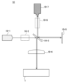
- FIG. 2 is a basic configuration diagram of an imaging system for acquiring a white interference microscopic image.
- FIG. 2 is a basic configuration diagram of an imaging system for acquiring confocal microscopic images.
- FIG. 2 is a basic configuration diagram of an imaging system for acquiring images using a photometric stereo method.
- FIG. 2 is a perspective view showing the configuration of a stage system.
- FIG. 2 is a configuration diagram seen from the front along the Y axis, showing the relationship between the imaging system and the object to be measured.
- FIG. 2 is a configuration diagram seen from the front along the X-axis, showing the relationship between the imaging system and the object to be measured.
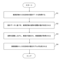
- FIG. 2 is a flowchart showing a procedure for measuring a three-dimensional shape of an object to be measured using a shape measuring device.
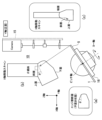
- FIG. 3 is an explanatory diagram of a procedure for measuring a three-dimensional shape of a notch portion of an object to be measured, which is a wafer.
- FIG. 6 is an explanatory diagram showing a method for acquiring a surface image when data is missing.
- FIG. 3 is a Y-axis front view showing the relationship between the imaging system and the object to be measured when measuring the edge portion of the outer periphery.
- FIG. 6 is an X-axis front view showing the relationship between the imaging system and the object to be measured when acquiring a surface image of the slope of the edge portion of the outer periphery.
- FIG. 3 is an explanatory diagram of a procedure for measuring a three-dimensional shape of a notch portion of an object to be measured, which is a wafer.
- FIG. 6 is an explanatory diagram showing a method for
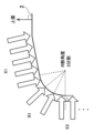
- FIG. 7 is a detailed view showing the cross-sectional shape and imaging direction of the outer peripheral edge portion.
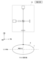
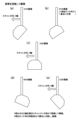
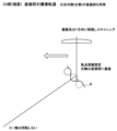
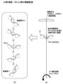
- FIG. 7 is an explanatory diagram of posture adjustment when acquiring a surface image of an edge portion of the outer periphery. It is a figure which shows the imaging trajectory of the one R part of X3 (end surface) in a notch part. It is a figure which shows the imaging trajectory of the straight part of X3 (end surface) in a notch part. It is a figure which shows the imaging trajectory of the bottom R part of X3 (end face) in a notch part.
- the embodiments shown below are examples that embody the technical idea of the present invention, and the technical idea of the present invention is based on the embodiments shown below. It is not specific to Furthermore, the drawings are schematic. Therefore, the relationships, ratios, etc. between thickness and planar dimensions may differ from those in reality, and the relationships and ratios between dimensions may also differ between drawings.
- a shape measuring device acquires a plurality of surface images while scanning the surface of a plate-shaped object to be measured, and measures the shape of the object to be measured.
- This is a shape measuring device for measuring the object, which includes an imaging system that irradiates the object to be measured with parallel light and obtains the surface image, and an imaging system that holds the object to be measured and a posture of the object with respect to the imaging system. and a control device, the control device controls the imaging system and the stage system to scan the surface while adjusting the attitude, and scans the surface while adjusting the attitude, and controls the imaging system and the stage system to scan the surface while adjusting the attitude.
- the posture adjustment unit includes an attitude adjustment unit that acquires an image, and an image processing unit that generates a restored model of the three-dimensional shape of the object from the plurality of acquired surface images, and the attitude adjustment unit includes:
- the shape measuring device adjusts the posture of the object to be measured so that the angle of incidence of the parallel light on the surface falls within a predetermined range when acquiring the surface image.
- FIG. 1 is a functional block diagram of the present shape measuring device.
- the shape measuring device 100 includes a stage system 30 that holds a plate-shaped object to be measured 1 (typically, a work-in-progress after various processes and/or a product wafer is preferable) and controls its posture; It includes an imaging system 10 that irradiates parallel light onto the measurement object 1 and acquires a surface image, and a control device 20.
- the control device 20 controls the imaging system 10 and the stage system 30 to scan the surface of the object to be measured 1 while adjusting the attitude of the object to be measured, and to acquire a plurality of surface images.
- It has an image processing unit 22 that generates a restored model of the three-dimensional shape of the measurement object 1.
- the material, shape, size, etc. of the plate-shaped object to be measured 1 are not particularly limited, but typically a semiconductor wafer (also simply referred to as a "wafer") is preferable.
- the semiconductor wafer may be one that is cut out from an ingot; one that has undergone various processes such as grinding, etching, and polishing; or a finished product that has undergone each process.
- the material is not particularly limited, and may be any of single crystal silicon, sapphire, silicon carbide, gallium phosphide (GaP), gallium arsenide (GaAS), indium phosphide (InP), gallium nitride (GaN), etc. It may be.
- the imaging system 10 has a function of irradiating the object to be measured 1 with parallel light and acquiring a surface image of the object to be measured 1 . It is preferable that the imaging system 10 typically includes a camera, a collimated light source, a beam splitter, and a condensing optical system. Note that the shape measuring device 100 in FIG. 1 includes one imaging system 10. However, the shape measuring device 100 of the present invention may have a plurality of imaging systems 10, and in that case, the shape measuring device 100 has an imaging system switching mechanism for switching and using the plurality of imaging systems 10. You can leave it there.
- each of the imaging systems 10 is used properly depending on the type of the object to be measured 1. Specifically, it is preferable that the control device 20 switches to a predetermined imaging system 10 based on the correspondence with the object to be measured 1.
- the object to be measured 1 is a wafer that has been subjected to a grinding process
- the surface of the object to be measured 1 has many grinding marks caused by the grinding tool, and the light irradiated onto the surface of the object to be measured 1 is diffusely reflected. There are many.
- the surface of the wafer after the grinding process has a surface state in which diffuse reflection is dominant.
- FIG. 2 is a basic configuration diagram of the imaging system 10 for acquiring white interference microscopic images.
- a light source 10-1 laser or light-emitting diode: LED
- a collimating optical system 10-2 for example, a beam expander, etc.
- the light passes through the objective lens 10-4 and is irradiated onto the object to be measured 1.
- the light source 10-1 may be a parallel light source, and in that case, the imaging system 10 does not need to have the collimating optical system 10-2.
- the camera 10-7 captures light reflected from the object to be measured 1 and passed through an objective lens 10-4, a beam splitter 10-3, a condensing optical system 10-6 (for example, a condensing lens, etc.), and a reference mirror.
- the light reflected by 10-5 and returned to the same optical path is imaged.
- a spatial interference pattern (interference fringes) is obtained.
- the interference fringes have information on the optical path difference between the two, and by analyzing the contrast changes and phase changes of the interference fringes that appear when the objective lens 10-4 is scanned in the vertical direction, surface unevenness shape data can be obtained. Can be obtained.
- the object to be measured 1 is a wafer that has undergone an etching process (e.g., alkaline etching process)
- the surface reflection characteristics may differ locally (coexist).
- FIG. 3 is a basic configuration diagram of the imaging system 10 for acquiring confocal microscopic images.
- the imaging system 10 for acquiring a confocal microscopic image acquires a three-dimensional image using an optical microscope that has a shallow depth of focus and uses a pinhole confocal optical system.
- the light from the light source 10-1 passes through the collimating optical system 10-2, which makes the diverging light parallel, the beam splitter 10-3, and the objective lens 10-4, and irradiates it onto the object to be measured 1, as in FIG. .
- Pinhole 10-8 is placed in front of light source 10-1 and camera 10-7. Therefore, the camera 10-7 images the light reflected from the object to be measured 1 and passed through the objective lens 10-4, beam splitter 10-3, condensing optical system 10-6, and pinhole 10-8.
- the out-of-focus image is blocked by the pinhole 10-8, and a strong signal is not obtained, and as a result, only the in-focus image is obtained.
- the beam is scanned in the horizontal direction and then scanned in the vertical direction in order to capture the surface.
- a focused image is typically acquired by the following procedure. Set the step interval in the vertical direction and obtain captured images of the surface at each height. At this time, the peak position of the photodetection intensity becomes the height of the surface of the target sample.
- This captured image is converted into three-dimensional surface shape data and saved by an image processing unit 22, which will be described later.
- the object to be measured 1 is a wafer that has been subjected to polishing processing
- the surface is prepared in a mirror-like state, so that direct reflection becomes dominant.
- an imaging system 10 for acquiring images by photometric stereo method using a polarizing plate.
- FIG. 4 is a basic configuration diagram of an imaging system 10 for acquiring images using the photometric stereo method.
- a normal vector which is three-dimensional shape information of an object surface
- the surface of the object to be measured 1 is a mirror surface
- direct reflection becomes dominant.
- the light from the light source 10-1 passes through the polarizing plate 10-9, the collimating optical system 10-2, the beam splitter 10-3, and the objective lens 10-4, and is irradiated onto the object to be measured 1.
- the camera 10-7 images the light reflected from the object to be measured 1 and passed through the objective lens 10-4, beam splitter 10-3, polarizing plate 10-10, and condensing optical system 10-6.
- the polarizing plate 10-9 and the polarizing plate 10-10 are arranged so that their polarization axes are perpendicular to each other at 90° (crossed nicol arrangement).
- the reflection of the light source 10-1 caused by the specularly reflected light (linearly polarized light) on the object to be measured 1 is removed, and only the diffusely reflected light (non-polarized light) reaches the camera 10-7.
- harmful "glare” or “shininess” caused by the reflection of the light source 10-1 is removed or reduced.
- the stage system 30 has the function of holding the object 1 to be measured and adjusting the attitude of the object 1 with respect to the imaging system 10, and typically has the function of It is preferable to include a chuck table having a five-axis structure including three axes and two axes, a yaw axis for rotation and a pitch axis for tilting.
- FIG. 5 is a perspective view showing the configuration of the stage system 30.
- the chuck table 16 that holds the object to be measured 1, which is a wafer, is a posture changing mechanism that can move in five axes, including two axes: the X axis, Y axis, Z axis, yaw axis, and pitch axis.
- a surface image can be obtained by irradiating the entire surface of the measurement object 1 with measurement light from the imaging system 10.
- FIG. 6 is a configuration diagram seen from the front on the Y axis, showing the relationship between the imaging system 10 and the object to be measured 1.
- the imaging system 10 shown in FIGS. 2, 3, and 4 is fixed to a baseboard 15.
- the chuck table 16 that holds the object to be measured 1 and changes its posture is preferably of a vacuum chuck type, and has two axes: a yaw axis for rotation and a pitch axis for tilting in addition to the three axes: X, Y, and Z axes. It has a 5-axis structure with the addition of Thereby, the surface of the object to be measured 1 can be scanned gradually at the scan pitch P in the X-axis direction to obtain a surface image.
- the edge portion 5 of the outer circumferential portion of the object to be measured 1 is arranged so that the pitch axis is rotated with respect to the slope and the end surface so that the irradiation surface by the imaging system 10 is perpendicular (in other words, the angle of incidence is 0°). imaged). Further, the outer circumferential portion can be imaged all around by rotating the yaw axis by 360 degrees.
- the imaging system 10 may have a configuration in which the baseboard 15 can be moved in the X-axis, Y-axis, and Z-axis directions.
- FIG. 7 is a configuration diagram seen from the front along the X-axis, showing the relationship between the imaging system 10 and the object to be measured 1.
- the surface of the object to be measured 1 is scanned with measurement light, which is parallel light, gradually at a scan pitch P in the Y-axis direction to obtain a surface image.
- the edge portion 5 on the outer periphery is imaged by rotating the pitch axis so that the irradiation surface is vertical (in other words, the incident angle is 0°).
- the outer circumference can be processed around the yaw axis by rotating it 360 degrees.
- control device 20 is typically a computer having a CPU (Central Processing Unit), a memory, etc., and when the CPU executes a program stored in the memory, the posture adjustment unit 21, In addition, the functions of the image processing section 22 are realized.
- CPU Central Processing Unit
- the attitude adjustment unit 21 has a function of controlling the stage system 30 to control the attitude of the object to be measured 1, and is realized by the CPU executing a program stored in the memory of the control device 20. When acquiring a surface image, the attitude adjustment unit 21 adjusts the attitude of the object to be measured 1 so that the angle of incidence of parallel light to the surface of the object to be measured 1 is within a predetermined range. Adjust.
- the imaging angle (incidence angle of parallel light) at which an accurate image can be obtained differs depending on the optical system (imaging method) of the imaging system 10.
- the Mirau type and the Michelson type are known, but both are limited to the range of imaging angles that allow accurate images to be acquired.
- This shape measuring device 100 has an attitude adjustment unit 21, and adjusts the incident angle of parallel light to the surface (imaging angle) to be within a predetermined range according to the imaging system 10, so that it is more accurate. images can be obtained.
- the specific angle of incidence is not particularly limited, it is generally preferably 0 to 30°, more preferably 0 to 15°, and in one preferred embodiment, the angle of incidence is approximately 0°.
- the method by which the attitude adjustment unit 21 performs the above adjustment is not particularly limited, but the amount of adjustment is determined based on the design data of the three-dimensional shape of the object to be measured 1 stored in advance in the memory of the control device 20. It is preferable to carry out the method by
- the design data for the three-dimensional shape of the object to be measured may be a design drawing (specification) of the product wafer.
- This design data may typically include data on the outer shape of the wafer (the outer periphery and the notch) and the three-dimensional shape of the notch.
- an example is a form of a point group expressed in a three-dimensional orthogonal coordinate system.
- the image processing unit 22 has a function of generating a restored model of the three-dimensional shape of the object to be measured 1 from a plurality of surface images acquired while scanning the surface of the object to be measured 1, and has a function of generating a restored model of the three-dimensional shape of the object to be measured 1. This is realized by the CPU executing a program stored in the CPU.
- Surface images for three-dimensional reconstruction are obtained by using, for example, a laser beam as observation light (measuring light) and extracting in-focus areas from multiple images obtained from an all-focal microscope system, that is, an image sensor. Combine. Further, a high-resolution super-depth image can be obtained by generating an all-in-focus image in which all positions are in focus.
- the photometric stereo method can also be used in conjunction with detailed shape measurement of a relatively small portion of unevenness (a small difference in height due to inclination, for example, a difference in height of 10 nanometers).
- FIG. 8 is a flowchart showing a procedure for measuring the three-dimensional shape of the object to be measured using the shape measuring apparatus 100.
- step S1 design data of the three-dimensional shape of the object to be measured is acquired.
- the data acquisition method is not particularly limited, and may be a form in which the CPU reads out design data stored in memory in advance depending on the type of the object to be measured, or Depending on the situation, input may be provided from outside.
- step S2 the amount of adjustment of the attitude of the object to be measured 1 is determined by the attitude adjustment unit 21 controlled by the control device 20 based on the design data.
- the locus of movement of the object to be measured 1 with respect to the imaging system 10 is calculated.
- step S3 the attitude adjustment unit 21 controls the imaging system 10 and the stage system 30 based on the imaging trajectory calculated in step S2, and the surface of the object 1 is scanned while adjusting the attitude of the object 1.
- a surface image of the object to be measured 1 is obtained.
- the imaging position is adjusted so as to scan the surface of the object to be measured 1, so that images covering a wide range of the surface of the object to be measured 1 are acquired.
- the imaging system 10 may also be moved. By doing so, posture adjustment can be performed more efficiently.
- step S4 a three-dimensional restored model is formed by the image processing unit 22 from the plurality of surface images obtained in step S3.
- FIG. 9 is an explanatory diagram of the procedure for measuring the three-dimensional shape of the notch portion 4 of the object to be measured 1, which is a wafer.
- semiconductor wafer production sites have been required to improve the quality of the shape and other areas down to the periphery, and in particular, the shape of the notch portion 4 is prone to deformation due to processes such as grinding, etching, and polishing. This affects the yield in post-processes.
- FIG. 9(a) is a plan view of the notch portion 4, and FIG. 9(b) is a cross-sectional view of the notch portion 4 taken along a dashed line.
- the notch part 4 has a complicated three-dimensional shape, and from the left end of FIG. It continues to a (2') straight line part where the curves are different, and a (1') piece R part that is symmetrical to the (1) piece R part.
- the cross-sectional shape first has an end surface X3 that is perpendicular to the upper surface 2 or lower surface 3 of the object to be measured 1, which is a wafer. Slopes X1 and X2 are formed at both ends of this end surface X3, and R1 and R2 are connected to these slopes (see FIG. 9(b)). X1, X2 and R1, R2 are symmetrical with respect to the midpoint of X3. The upper surface 2 or lower surface 3, end surface X3, and slopes X1 and X2 of the object to be measured 1 have different crystal orientations. Note that the cross-sectional shape in FIG. 9(b) is the same not only in the notch portion 4 but also in the edge portion 5 of the outer peripheral portion, and is constant over one circumference.
- the postures of the imaging system 10 and the object to be measured 1 are changed according to the notch shape.
- the imaging system 10 (the angle of incidence of parallel light) is made perpendicular to the surface shape of the notch portion 4 .
- the attitude adjustment unit 21 calculates the amount of attitude adjustment (imaging trajectory) of the object 1 to be measured by the stage system 30 (step S2). Thereby, the surface of the notch portion 4 of the imaging system 10 is also made vertical.
- the amount of posture adjustment is selected from the following two viewpoints as one form.
- One is to make the focal length of the imaging system 10 constant based on the information of the design data (point group data based on an orthogonal coordinate system, etc.) acquired in step S1.
- the other is to make sure that the incident angle of the irradiated parallel light falls within a predetermined range.
- the attitude adjustment amount is determined by optimizing the optical imaging (image acquisition) conditions of the surface shape according to the surface condition of the object to be measured 1, based on the three-dimensional coordinates of the notch-shaped surface to which the design values are given. It is determined.
- the imaging trajectory of the object to be measured 1 is controlled based on the determined attitude adjustment amount, and a surface image of the object to be measured 1 is acquired.
- the chuck table 16 that holds the object 1 to be measured and changes its posture is preferably of a vacuum chuck type.
- the present shape measuring apparatus 100 can image a sharply uneven surface while adjusting the attitude of the object 1 by moving the chuck table 16 in five axes and using the attitude adjustment mechanism. This allows the angle of the imaging system 10 (the angle of incidence of the irradiation light) to be within a predetermined range with respect to the surface shape. Therefore, it is possible to image the accurate surface shape of the object to be measured 1 (obtain a surface image).
- the slope shape of the surface of the object to be measured 1 can also be measured more accurately by examining the amount of reflected light from the surface irradiated with measurement light, which is parallel light.
- Step S3 After the processing in step S3, depth coordinates, which are three-dimensional coordinates, are obtained from the plurality of acquired surface images, three-dimensional restoration is performed, and a restored model is created. (Step S4) After the restored model is created, it may be used for determining the quality of the master wafer (workpiece) and for shape conditions in post-processing.
- Surface images for three-dimensional reconstruction are obtained by using, for example, a laser beam as observation light (measuring light) and extracting in-focus areas from multiple images obtained from an all-focal microscope system, that is, an image sensor. This can be done by combining them. Further, a high-resolution super-depth image can be obtained by generating an all-in-focus image in which all positions are in focus.
- the photometric stereo method can also be used in conjunction with detailed shape measurements of relatively small uneven portions (small elevation differences due to inclination, for example, elevation differences of about 10 nanometers).
- FIG. 10 is an explanatory diagram showing a method for acquiring a surface image when data is missing. If the slope of the surface irregularities is large, or if there are defects such as irregular etch pits, data may be missing.
- existing optical surface texture measuring instruments have a numerical aperture NA of approximately 0.55, which represents the light collection limit in the absence of aberrations. If the angle is 7.9° or more, the lens may not be able to capture a portion of the reflected light from the surface to be measured due to angle followability, which may result in data loss.
- the pitch angle of the surface to be measured is rotated in steps of 7 degrees or less to obtain a plurality of surface images taken at different imaging angles from the same location. If the surface to be measured has undulations (irregularities) as shown in Fig. 10(a), rotate the surface to be measured counterclockwise as shown in the surface image in Fig. 10(a) and Fig. 10(b). The surface image obtained by rotating the surface to be measured clockwise as shown in FIG. 10(c) is combined to integrate the obtained images. As a result, the surface image of the area of interest is obtained as a consistent shape with no missing data.
- FIG. 11 is a Y-axis front view showing the relationship between the imaging system 10 and the object to be measured 1 when measuring the edge portion 5 on the outer periphery.
- the cross section of the edge portion 5 has a slope (angle ⁇ ) as shown in FIG. 11(a) when the edge portion 5 is placed flat.
- FIG. 11(b) is a diagram showing the measurement state of the slope.
- the attitude adjustment unit 21 rotates the chuck table 16 around the pitch axis so that the irradiation surface by the imaging system 10 is vertical (in other words, the angle of incidence is approximately 0°), and the imaging system 10 in the X-axis direction, the imaging system 10 is caused to acquire a surface image.
- FIG. 11(c) shows the irradiation state of the end surface. Similar to FIG. 11(b), the pitch axis is rotated so that the incident angle of the parallel light is approximately 0° (within a predetermined range). is obtained. Furthermore, the chuck table 16 is rotated 360 degrees around the yaw axis to obtain a surface image of the outer periphery.
- FIG. 12 is an X-axis front view showing the relationship between the imaging system 10 and the object to be measured 1 when acquiring a surface image of the slope of the edge portion 5 on the outer periphery.
- the object to be measured 1 is held on a chuck table 16 similar to that shown in FIG.
- the attitude adjustment unit 21 adjusts the measurement target around the pitch axis and the tilt axis so that the incident angle of parallel light is within a predetermined range (for example, approximately 0°).
- the posture of the object 1 is controlled and a surface image is acquired. Note that the irradiation conditions may be determined depending on the crystal orientation and shape.
- FIG. 13 is a detailed view showing the cross-sectional shape and imaging direction of the edge portion 5 on the outer periphery.
- the arrow indicates the direction of incidence of parallel light by the imaging system 10.
- the cross-sectional shape changes from the upper surface 2 of the object to be measured 1 to an inclined surface X1, an R portion R1, and reaches an end surface X3 perpendicular to the upper surface 2.
- FIG. 14 is an explanatory diagram of posture adjustment when acquiring a surface image of the outer edge portion 5.
- the pitch axis is rotated at each part of the edge part 5 (each part explained in FIG. 9(b)), the incident angle is adjusted, and the surface is traced. This is done by scanning.
- FIG. 14(a) shows the attitude control method when acquiring the surface image of X1
- FIG. 14(c) shows the surface image of X3
- FIG. 14(e) shows the attitude control method when acquiring the surface image of X2.
- R1 in FIG. 14(b) and R2 in FIG. 14(d) indicate imaging of the R section, in which the pitch axis is divided into rotational increments of a predetermined pitch angle. For example, R1 and R2 are 60 to 70 degrees. Therefore, it is preferable to divide the image into three parts.
- FIG. 15 is a diagram showing the imaging trajectory of the (1′) piece R portion (see FIG. 9(b)) of X3 (end surface) in the notch portion 4.
- the attitude adjustment unit 21 fixes the focal length of the imaging system and (1') passes through the center of the R part, as shown in FIG. 15(a).
- An imaging system is placed on the optical axis, and the yaw axis of the chuck table 16 is rotated to acquire a surface image.
- (1') By placing the imaging system on the optical axis passing through the center of the R-side portion, the arc of the R-side portion and the direction of incidence of parallel light become approximately perpendicular.
- the entire one R section is scanned (scanned in the Z-axis and Y-axis directions) while adjusting the incident angle within a predetermined range to obtain a surface image. be able to. Then, when the surface image of the rounded portion is acquired in the above manner, it reaches the straight portion (2') as shown in FIG. 15(b). Note that the symmetrical (1) piece R portion is the same.
- FIG. 16 is a diagram showing the imaging trajectory of the (2') straight section (see FIG. 9(b)) of X3 (end surface) in the notch portion 4.
- the surface image of the linear portion of the notch portion 4 is obtained by scanning in the Y-axis direction, fixing the focal length and the yaw axis, and adjusting the incident angle, as shown in FIG.
- FIG. 17 is a diagram showing the imaging trajectory of the (3) bottom R portion of X3 (end surface) in the notch portion 4.
- the surface image of the bottom R part of the notch part is obtained by fixing the focal length of the imaging system and controlling the rotation of the yaw axis to align the imaging system with the optical axis passing through the center of the bottom R part.
- the incident angle is adjusted to approximately 0°, and the image is acquired while scanning in the Z-axis direction and the Y-axis direction.
- the surface image of the object to be measured 1 is set to the optimum conditions according to the shape of the object to be measured 1 by the attitude adjustment section 21, so even if the surface image is a complex three-dimensional shape like the notch section 4, It is also possible to perform shape measurements with high accuracy.
Landscapes
- Engineering & Computer Science (AREA)
- Physics & Mathematics (AREA)
- General Physics & Mathematics (AREA)
- Computer Vision & Pattern Recognition (AREA)
- Theoretical Computer Science (AREA)
- Multimedia (AREA)
- Signal Processing (AREA)
- Length Measuring Devices By Optical Means (AREA)
- Testing Or Measuring Of Semiconductors Or The Like (AREA)
- Manufacturing & Machinery (AREA)
Abstract
Description
光投影測定法は、ウェハの面取り加工された端部に対し、そのウェハの表裏各面に略平行な方向から光を投光すると共に、その投光方向に対向する方向からカメラによってウェハの端面の投影像(厚み方向に切断した断面形状)を撮像するものである。
[2] 上記姿勢調整部は、予め記憶された上記被測定物の3次元形状の設計データをもとに、上記調整の量を決定する、[1]に記載の形状測定装置。
[3] 上記ステージ系は、X軸、Y軸、Z軸の3軸に加えて、回転のヨー軸と傾斜のピッチ軸の2軸を加えた5軸による構造のチャックテーブルを含む、[1]又は[2]に記載の形状測定装置。
[4] 複数の上記撮像系と、上記撮像系を切り替える、撮像系切り替え機構と、を有し、上記制御装置は、上記被測定物との対応関係に基づき予め定められた上記撮像系に、使用する上記撮像系を切り替える、[1]又は[2]に記載の形状測定装置。
[5] 上記被測定物がウェハであり、上記撮像系が、白色干渉顕微画像の取得用、共焦点顕微画像の取得用、及び、偏光板を利用した照度差ステレオ法による画像の取得用からなる群より選択される少なくとも2種以上を含み、上記制御装置は、上記ウェハが研削処理後のウェハである場合、白色干渉顕微画像の取得用の上記撮像系に、上記ウェハがエッチング処理後のウェハである場合、共焦点顕微画像の取得用の上記撮像系に、上記ウェハが研磨処理後のウェハである場合、照度差ステレオ法による画像の取得用の上記撮像系に、それぞれ切り替える、[4]に記載の形状測定装置。
[6] 上記被測定物がウェハであり、上記姿勢調整部は、上記ウェハのエッジ部の上記表面画像の取得に際し、斜面、又は、端面に対して上記ピッチ軸を回転させて、上記入射角を調整し、かつ、上記撮像系を上記X軸の方向に走査しながら、上記表面画像を取得させ、次いで、上記ヨー軸を回転させて外周の上記表面画像を取得させる、[3]に記載の形状測定装置。
[7] 上記ウェハのR部の上記表面画像の取得に際し、上記姿勢調整部は、上記ピッチ軸を所定のピッチ角の回転刻みで分割し、上記表面画像を取得させる、[6]に記載の形状測定装置。
[8] 上記被測定物がウェハであり、上記姿勢調整部は、上記ウェハのノッチ部の片R部の上記表面画像の取得に際し、上記撮像系の焦点距離を固定し、上記片R部の中心を通る光軸に上記撮像系を置き、上記ヨー軸を回転させて、上記表面画像を取得させる、[3]に記載の形状測定装置。
[9] 上記被測定物がウェハであり、上記姿勢調整部は、ノッチ部の直線部の上記表面画像の取得に際し、上記撮像系の焦点距離、及び、上記ヨー軸を固定し、上記入射角を調整する、[3]に記載の形状測定装置。
[10] 上記被測定物がウェハであり、上記姿勢調整部は、上記ウェハのノッチ部のボトムR部の上記表面画像の取得に際し、上記撮像系の焦点距離を固定し、上記ボトムR部の中心を通る光軸に上記撮像系を置き、上記Z軸の方向、及び、上記Y軸の方向に走査しながら、上記表面画像を取得させる、[3]に記載の形状測定装置。
以下に記載する構成要件の説明は、本発明の代表的な実施形態に基づいてなされることがあるが、本発明はそのような実施形態に制限されるものではない。
なお、本明細書において、「~」を用いて表される数値範囲は、「~」の前後に記載される数値を下限値及び上限値として含む範囲を意味する。
本発明の実施形態に係る形状測定装置(以下「本形状測定装置」ともいう。)は、板状の被測定物の表面を走査しながら複数の表面画像を取得し、上記被測定物の形状を測定するための形状測定装置であって、被測定物に平行光を照射し、上記表面画像を取得する撮像系と、上記被測定物を保持し、上記撮像系に対する上記被測定物の姿勢を調整するステージ系と、制御装置と、を有し、上記制御装置は、上記撮像系、及び、上記ステージ系を制御して、上記姿勢を調整しながら上記表面を走査させ、複数の上記表面画像を取得させる、姿勢調整部と、取得された複数の上記表面画像から、上記被測定物の3次元形状の復元モデルの生成を行う画像処理部と、を有し、上記姿勢調整部は、上記表面画像の取得に際し、上記平行光の上記表面への入射角が予め定めた範囲内となるよう、上記被測定物の姿勢を調整する、形状測定装置である。
なお、図1の形状測定装置100は、撮像系10を1つ有している。しかし、本発明の形状測定装置100が有する撮像系10は、複数であってもよく、その場合、形状測定装置100は複数の撮像系10を切り替えて使用するための撮像系切り替え機構を有していてもよい。
このような場合、表面画像をより正確、より効率的に取得するためには、共焦点顕微画像の取得用の撮像系10を用いることが好ましい。
このような場合、表面画像をより正確、より効率的に取得するためには、偏光板を利用した照度差ステレオ法による画像の取得用の撮像系10を用いることが好ましい。
被測定物1の表面は鏡面であると、直接反射が支配的になる。このとき、白色干渉顕微画像の取得用の光学系、共焦点顕微画像の取得用の光学系では、正確な画像の取得が困難であり、照度差ステレオ法を用いた上で光沢による輝度の高い部分であるハイライトを除去することが好ましい。
図2、3、4で示した撮像系10は、ベースボード15に固定される。被測定物1を保持して姿勢を可変するチャックテーブル16は、真空チャック方式が望ましく、X軸、Y軸、Z軸の3軸に加えて、回転のヨー軸と傾斜のピッチ軸の2軸を加えた5軸構造とされている。これにより、被測定物1の表面は、X軸方向にスキャンピッチPをとって漸次走査して表面画像を取得することができる。
本形状測定装置100は、姿勢調整部21を有し、撮像系10に応じて、表面に対する平行光の入射角(撮像角度)が予め定められた範囲内となるよう調整されるため、より正確な画像を取得することができる。
具体的な入射角度は特に制限されないが、一般に、0~30°が好ましく、0~15°がより好ましく、好ましい一形態としては、入射角は、略0°である。
被測定物の3次元形状の設計データとしては、例えば、被測定物1がウェハである場合、製品ウェハの設計図(仕様)であってよい。この設計データには、典型的には、ウェハの外形(外周部、及び、ノッチ部)、及び、ノッチの3次元形状のデータが含まれていてもよい。具体的には、三次元直交座標系で表現された点群である形態が挙げられる。
図8は、本形状測定装置100による被測定物の3次元形状の測定手順を示すフローチャートである。
まず、ステップS1として、被測定物の3次元形状の設計データが取得される。データの取得方法としては特に制限されず、被測定物の種類に対応して、予めメモリに記憶されている設計データをCPUが読み出す形態であってもよいし、測定される被測定物1に応じて、外部から入力されてもよい。
図9は、ウェハである被測定物1のノッチ部4の3次元形状の測定の手順の説明図である。近年、半導体ウェハ生産現場は、周縁に至る領域まで形状等の品質を向上させることを求められており、特に、ノッチ部4の形状は研削・エッチング・研磨等のプロセスにより形状くずれを起こし易く、後工程での歩留まりに影響している。
被測定物1を保持して姿勢を可変するチャックテーブル16は、真空チャック方式が好ましい。一形態として、X軸、Y軸、Z軸の3軸に加えて、回転のヨー軸と傾斜のピッチ軸の2軸を加えた5軸構造とすることが好ましい。
復元モデルが作成された後は、マスターウェハ(ワーク)に対する良否判定、後工程の形状条件に利用されてもよい。
姿勢調整部21は、チャックテーブル16をピッチ軸回りに回転させて、撮像系10による照射面が垂直になるように(言い換えれば、入射角が略0°となるように)、かつ、撮像系10をX軸方向に走査しながら、撮像系10に表面画像を取得させる。
更に、外周部は、チャックテーブル16をヨー軸回りに360度回転させて、外周の表面画像が取得される。
図14(b)のR1、図14(d)のR2は、R部の撮像を示しており、ピッチ軸を所定のピッチ角の回転刻みで分割し、例えばR1、R2は60~70°であるので3分割して撮像することが好ましい。
(1’)片R部の中心を通る光軸に撮像系を置くことで、片R部の円弧と、平行光の入射方向とが略垂直となる。すなわち、上述のとおり姿勢調整を行うことで、入射角を所定の範囲内に調整しながら、片R部の全体を走査して(Z軸、Y軸方向に走査して)表面画像を取得することができる。
そして、上記によって、片R部の表面画像が取得されると、図15(b)のように(2’)直線部へ至る。なお、対称となっている(1)片R部は、同様である。
Claims (10)
- 板状の被測定物の表面を走査しながら複数の表面画像を取得し、前記被測定物の形状を測定するための形状測定装置であって、
前記被測定物に平行光を照射し、前記表面画像を取得する撮像系と、
前記被測定物を保持し、前記撮像系に対する前記被測定物の姿勢を調整するステージ系と、制御装置と、を有し、
前記制御装置は、
前記撮像系、及び、前記ステージ系を制御して、前記姿勢を調整しながら前記表面を走査させ、複数の前記表面画像を取得させる、姿勢調整部と、
取得された複数の前記表面画像から、前記被測定物の3次元形状の復元モデルの生成を行う画像処理部と、を有し、
前記姿勢調整部は、前記表面画像の取得に際し、前記平行光の前記表面への入射角が予め定めた範囲内となるよう、前記姿勢を調整する、形状測定装置。 - 前記姿勢調整部は、予め記憶された前記被測定物の3次元形状の設計データをもとに、前記調整の量を決定する、請求項1に記載の形状測定装置。
- 前記ステージ系は、X軸、Y軸、Z軸の3軸に加えて、回転のヨー軸と傾斜のピッチ軸の2軸を加えた5軸による構造のチャックテーブルを含む、請求項1又は2に記載の形状測定装置。
- 複数の前記撮像系と、
前記撮像系を切り替える、撮像系切り替え機構と、を有し、
前記制御装置は、前記被測定物との対応関係に基づき予め定められた前記撮像系に、使用する前記撮像系を切り替える、請求項1又は2に記載の形状測定装置。 - 前記被測定物がウェハであり、
前記撮像系が、白色干渉顕微画像の取得用、共焦点顕微画像の取得用、及び、偏光板を利用した照度差ステレオ法による画像の取得用からなる群より選択される少なくとも2種以上を含み、
前記制御装置は、
前記ウェハが研削処理後のウェハである場合、白色干渉顕微画像の取得用の前記撮像系に、
前記ウェハがエッチング処理後のウェハである場合、共焦点顕微画像の取得用の前記撮像系に、
前記ウェハが研磨処理後のウェハである場合、照度差ステレオ法による画像の取得用の前記撮像系に、それぞれ切り替える、請求項4に記載の形状測定装置。 - 前記被測定物がウェハであり、
前記姿勢調整部は、前記ウェハのエッジ部の前記表面画像の取得に際し、
斜面、又は、端面に対して前記ピッチ軸を回転させて、前記入射角を調整し、かつ、前記撮像系を前記X軸の方向に走査しながら、前記表面画像を取得させ、
次いで、前記ヨー軸を回転させて外周の前記表面画像を取得させる、請求項3に記載の形状測定装置。 - 前記ウェハのR部の前記表面画像の取得に際し、
前記姿勢調整部は、前記ピッチ軸を所定のピッチ角の回転刻みで分割し、前記表面画像を取得させる、請求項6に記載の形状測定装置。 - 前記被測定物がウェハであり、
前記姿勢調整部は、前記ウェハのノッチ部の片R部の前記表面画像の取得に際し、
前記撮像系の焦点距離を固定し、前記片R部の中心を通る光軸に前記撮像系を置き、前記ヨー軸を回転させて、前記表面画像を取得させる、請求項3に記載の形状測定装置。 - 前記被測定物がウェハであり、
前記姿勢調整部は、ノッチ部の直線部の前記表面画像の取得に際し、
前記撮像系の焦点距離、及び、前記ヨー軸を固定し、前記入射角を調整する、請求項3に記載の形状測定装置。 - 前記被測定物がウェハであり、
前記姿勢調整部は、前記ウェハのノッチ部のボトムR部の前記表面画像の取得に際し、前記撮像系の焦点距離を固定し、前記ボトムR部の中心を通る光軸に前記撮像系を置き、前記Z軸の方向、及び、前記Y軸の方向に走査しながら、前記表面画像を取得させる、請求項3に記載の形状測定装置。
Priority Applications (3)
| Application Number | Priority Date | Filing Date | Title |
|---|---|---|---|
| CN202380023906.2A CN118765365A (zh) | 2022-03-09 | 2023-02-03 | 形状测定装置 |
| US18/845,314 US12456217B2 (en) | 2022-03-09 | 2023-02-03 | Shape measurement device |
| KR1020247029093A KR20240142522A (ko) | 2022-03-09 | 2023-02-03 | 형상측정장치 |
Applications Claiming Priority (2)
| Application Number | Priority Date | Filing Date | Title |
|---|---|---|---|
| JP2022-035892 | 2022-03-09 | ||
| JP2022035892A JP7798615B2 (ja) | 2022-03-09 | 2022-03-09 | 形状測定装置 |
Publications (1)
| Publication Number | Publication Date |
|---|---|
| WO2023171192A1 true WO2023171192A1 (ja) | 2023-09-14 |
Family
ID=87936712
Family Applications (1)
| Application Number | Title | Priority Date | Filing Date |
|---|---|---|---|
| PCT/JP2023/003617 Ceased WO2023171192A1 (ja) | 2022-03-09 | 2023-02-03 | 形状測定装置 |
Country Status (5)
| Country | Link |
|---|---|
| US (1) | US12456217B2 (ja) |
| JP (2) | JP7798615B2 (ja) |
| KR (1) | KR20240142522A (ja) |
| CN (1) | CN118765365A (ja) |
| WO (1) | WO2023171192A1 (ja) |
Cited By (1)
| Publication number | Priority date | Publication date | Assignee | Title |
|---|---|---|---|---|
| WO2025126960A1 (ja) * | 2023-12-11 | 2025-06-19 | 株式会社東京精密 | 形状測定装置及び形状測定方法並びにウェーハ加工システム |
Families Citing this family (1)
| Publication number | Priority date | Publication date | Assignee | Title |
|---|---|---|---|---|
| US20250046636A1 (en) * | 2023-08-04 | 2025-02-06 | Jun-Fu Technology Inc | Robotic arm with vibration detection and image recognition |
Citations (3)
| Publication number | Priority date | Publication date | Assignee | Title |
|---|---|---|---|---|
| JP2003057016A (ja) * | 2001-08-10 | 2003-02-26 | Canon Inc | 高速大口径面形状測定方法および装置 |
| WO2016098469A1 (ja) * | 2014-12-16 | 2016-06-23 | 富士フイルム株式会社 | 形状測定装置及び形状測定方法 |
| JP6590429B1 (ja) * | 2018-12-25 | 2019-10-16 | レーザーテック株式会社 | 共焦点顕微鏡、及びその撮像方法 |
Family Cites Families (9)
| Publication number | Priority date | Publication date | Assignee | Title |
|---|---|---|---|---|
| EP1640453A4 (en) * | 2003-06-25 | 2009-09-02 | Nat Inst Of Advanced Ind Scien | DIGITAL CELL |
| JP4500157B2 (ja) | 2004-11-24 | 2010-07-14 | 株式会社神戸製鋼所 | 形状計測装置用光学系 |
| US7674610B2 (en) * | 2005-04-08 | 2010-03-09 | Abeygunaratne Thusara Sugat Chandra | Method and device for probing changes in a membrane by applying an in-plane electric field |
| JP4262285B2 (ja) | 2007-07-18 | 2009-05-13 | 株式会社コベルコ科研 | 形状測定装置,形状測定方法 |
| US8961877B2 (en) * | 2007-08-09 | 2015-02-24 | Massachusetts Institute Of Technology | High-throughput, whole-animal screening system |
| KR101658982B1 (ko) * | 2014-11-13 | 2016-09-26 | 주식회사 고영테크놀러지 | 회절 격자를 이용한 3차원 형상 측정 장치 |
| JP6953242B2 (ja) * | 2017-09-06 | 2021-10-27 | 株式会社ディスコ | 高さ検出装置、及びレーザー加工装置 |
| JP2021025910A (ja) * | 2019-08-06 | 2021-02-22 | 株式会社キーエンス | 三次元形状測定装置及び三次元形状測定方法 |
| JP7358185B2 (ja) * | 2019-10-15 | 2023-10-10 | 株式会社ディスコ | 厚み計測装置、及び厚み計測装置を備えた加工装置 |
-
2022
- 2022-03-09 JP JP2022035892A patent/JP7798615B2/ja active Active
-
2023
- 2023-02-03 US US18/845,314 patent/US12456217B2/en active Active
- 2023-02-03 CN CN202380023906.2A patent/CN118765365A/zh active Pending
- 2023-02-03 KR KR1020247029093A patent/KR20240142522A/ko active Pending
- 2023-02-03 WO PCT/JP2023/003617 patent/WO2023171192A1/ja not_active Ceased
-
2025
- 2025-12-25 JP JP2025281546A patent/JP2026062826A/ja active Pending
Patent Citations (3)
| Publication number | Priority date | Publication date | Assignee | Title |
|---|---|---|---|---|
| JP2003057016A (ja) * | 2001-08-10 | 2003-02-26 | Canon Inc | 高速大口径面形状測定方法および装置 |
| WO2016098469A1 (ja) * | 2014-12-16 | 2016-06-23 | 富士フイルム株式会社 | 形状測定装置及び形状測定方法 |
| JP6590429B1 (ja) * | 2018-12-25 | 2019-10-16 | レーザーテック株式会社 | 共焦点顕微鏡、及びその撮像方法 |
Cited By (1)
| Publication number | Priority date | Publication date | Assignee | Title |
|---|---|---|---|---|
| WO2025126960A1 (ja) * | 2023-12-11 | 2025-06-19 | 株式会社東京精密 | 形状測定装置及び形状測定方法並びにウェーハ加工システム |
Also Published As
| Publication number | Publication date |
|---|---|
| US12456217B2 (en) | 2025-10-28 |
| JP2023131261A (ja) | 2023-09-22 |
| JP2026062826A (ja) | 2026-04-10 |
| KR20240142522A (ko) | 2024-09-30 |
| US20250200777A1 (en) | 2025-06-19 |
| CN118765365A (zh) | 2024-10-11 |
| JP7798615B2 (ja) | 2026-01-14 |
Similar Documents
| Publication | Publication Date | Title |
|---|---|---|
| US8654352B1 (en) | Chromatic confocal scanning apparatus | |
| CN102037309B (zh) | 光学检查探头 | |
| TWI576563B (zh) | 非接觸式測量表面的方法及設備 | |
| JP2026062826A (ja) | 形状測定装置 | |
| US20070146685A1 (en) | Dynamic wafer stress management system | |
| KR100951221B1 (ko) | 렌즈에 있어서의 표리면의 광축 편심량의 측정 방법 | |
| US20120307259A1 (en) | Apparatus and method for inspecting an object with increased depth of field | |
| CN107850555B (zh) | 使用静态条纹图案的干涉法滚降测量 | |
| KR102687194B1 (ko) | 표면 변형들의 이미지 기반 계측 | |
| CN107525463A (zh) | 光干涉测定装置和光干涉测定方法 | |
| CN117110290B (zh) | 一种明暗场和白光干涉的缺陷检测系统和检测方法 | |
| TW202316563A (zh) | 用於絕對樣本定位之系統及方法 | |
| JP3678916B2 (ja) | 非接触三次元測定方法 | |
| JP2010528314A (ja) | 立体形状測定装置 | |
| JP2005070225A (ja) | 表面画像投影装置及び表面画像投影方法 | |
| JP5328025B2 (ja) | エッジ検出装置及びこれを用いた工作機械、エッジ検出方法 | |
| JP7304513B2 (ja) | 表面形状測定装置及び表面形状測定方法 | |
| KR20140078621A (ko) | 기판의 형상 변화 측정 방법 | |
| JP7085725B2 (ja) | 表面形状測定装置及び表面形状測定方法 | |
| KR101826127B1 (ko) | 광학적 웨이퍼 검사 장치 | |
| AU2014216740A1 (en) | A method and apparatus for quantitative measurement of surface accuracy of an area | |
| JP7733751B2 (ja) | レンズ貫通高さ測定 | |
| US20260050246A1 (en) | Shape model generation and use for semiconductor workpiece | |
| JP2005055217A (ja) | 高さ測定方法 | |
| JP3235782B2 (ja) | 位置検出方法及び半導体基板と露光マスク |
Legal Events
| Date | Code | Title | Description |
|---|---|---|---|
| 121 | Ep: the epo has been informed by wipo that ep was designated in this application |
Ref document number: 23766372 Country of ref document: EP Kind code of ref document: A1 |
|
| WWE | Wipo information: entry into national phase |
Ref document number: 202380023906.2 Country of ref document: CN |
|
| ENP | Entry into the national phase |
Ref document number: 20247029093 Country of ref document: KR Kind code of ref document: A |
|
| WWE | Wipo information: entry into national phase |
Ref document number: 18845314 Country of ref document: US |
|
| NENP | Non-entry into the national phase |
Ref country code: DE |
|
| 122 | Ep: pct application non-entry in european phase |
Ref document number: 23766372 Country of ref document: EP Kind code of ref document: A1 |
|
| WWP | Wipo information: published in national office |
Ref document number: 18845314 Country of ref document: US |
|
| WWG | Wipo information: grant in national office |
Ref document number: 18845314 Country of ref document: US |