WO2023162804A1 - メモリ装置およびメモリ制御方法 - Google Patents
メモリ装置およびメモリ制御方法 Download PDFInfo
- Publication number
- WO2023162804A1 WO2023162804A1 PCT/JP2023/005126 JP2023005126W WO2023162804A1 WO 2023162804 A1 WO2023162804 A1 WO 2023162804A1 JP 2023005126 W JP2023005126 W JP 2023005126W WO 2023162804 A1 WO2023162804 A1 WO 2023162804A1
- Authority
- WO
- WIPO (PCT)
- Prior art keywords
- memory
- refresh
- memory cell
- read
- cell array
- Prior art date
- Legal status (The legal status is an assumption and is not a legal conclusion. Google has not performed a legal analysis and makes no representation as to the accuracy of the status listed.)
- Ceased
Links
Images








Classifications
-
- G—PHYSICS
- G11—INFORMATION STORAGE
- G11C—STATIC STORES
- G11C13/00—Digital stores characterised by the use of storage elements not covered by groups G11C11/00, G11C23/00, or G11C25/00
-
- H—ELECTRICITY
- H10—SEMICONDUCTOR DEVICES; ELECTRIC SOLID-STATE DEVICES NOT OTHERWISE PROVIDED FOR
- H10B—ELECTRONIC MEMORY DEVICES
- H10B63/00—Resistance change memory devices, e.g. resistive RAM [ReRAM] devices
- H10B63/10—Phase change RAM [PCRAM, PRAM] devices
-
- H—ELECTRICITY
- H10—SEMICONDUCTOR DEVICES; ELECTRIC SOLID-STATE DEVICES NOT OTHERWISE PROVIDED FOR
- H10N—ELECTRIC SOLID-STATE DEVICES NOT OTHERWISE PROVIDED FOR
- H10N70/00—Solid-state devices having no potential barriers, and specially adapted for rectifying, amplifying, oscillating or switching
-
- G—PHYSICS
- G06—COMPUTING OR CALCULATING; COUNTING
- G06F—ELECTRIC DIGITAL DATA PROCESSING
- G06F12/00—Accessing, addressing or allocating within memory systems or architectures
Definitions
- the present disclosure relates to memory devices and memory control methods.
- each memory cell has a cell structure in which a storage element and a selection element are connected in series.
- a read error or write error may occur due to a change in operating voltage. In order to prevent such malfunctions, it is conceivable to perform a refresh operation.
- a memory device includes a nonvolatile memory cell array unit and a memory controller that controls write operations and read operations for the nonvolatile memory cell array unit.
- the memory controller uses at least one of write and read operations to control refresh operations for the nonvolatile memory cell array units.
- the memory controller further sets the refresh operation cycle based on at least one of the number of writes and the number of reads to the nonvolatile memory cell array unit.
- a memory control method includes the following two. (A) controlling the refresh operation for the non-volatile memory cell array unit by using at least one of the write operation and the read operation for the non-volatile memory cell array unit; setting the cycle of the refresh operation based on at least one of
- the refresh operation for the nonvolatile memory cell array unit using at least one of the write operation and the read operation for the nonvolatile memory cell array unit is controlled.
- the refresh operation using the read operation is performed, the refresh operation is not performed in the high-resistance memory cells.
- the refresh operation using the write operation is performed, the refresh operation is performed on any memory cell. Therefore, it is possible to prevent malfunction.
- the refresh operation cycle is set based on at least one of the number of writes and the number of reads to the nonvolatile memory cell array unit.
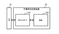
- FIG. 1 is a diagram illustrating an example of a schematic configuration of an information processing system including a nonvolatile storage device (memory device) according to an embodiment of the present disclosure
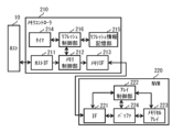
- FIG. 2 is a diagram showing an example of functional blocks of the nonvolatile memory device of FIG. 1
- FIG. 3 is a diagram showing an example of a schematic configuration of a memory cell array in FIG. 2
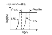
- FIG. 4 is a diagram showing an example of IV characteristics of the memory cell of FIG. 3
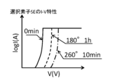
- FIG. FIG. 4 is a diagram showing an example of IV characteristics of the selection element of FIG. 3
- FIG. 4 is a diagram showing an example of threshold variation of the selection element of FIG. 3
- FIG. 4 is a diagram showing an example of threshold variation of the selection element of FIG. 3
- FIG. 3 is a diagram illustrating an example of threshold variation of the selection element of FIG. 3;
- FIG. 3 is a diagram illustrating an example of threshold variation of the selection element of FIG. 3;
- FIG. 4 is a diagram showing an example of threshold variation of the selection element of FIG. 3;
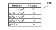
- FIG. 10 is a diagram showing an example of a refresh operation table in which operation counts and refresh times are described;
- FIG. 10 is a diagram showing an example of a refresh cycle table in which the correspondence relationship between the number of operations and refresh cycles is defined;
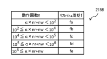
- FIG. 10 is a diagram showing a modified example of a refresh table in which the number of operations and refresh times are defined;
- FIG. 10 is a diagram showing a modified example of a refresh cycle table in which correspondence relationships between operation counts and refresh cycles are defined;
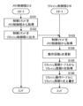
- FIG. 10 is a diagram illustrating an example of a refresh cycle update procedure;
- FIG. 10 is a diagram showing an example of a procedure for outputting a refresh command;
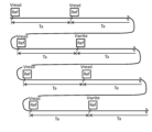
- FIG. 4 is a diagram illustrating an example of refresh control
- FIG. FIG. 11 is a diagram illustrating a modified example of refresh control
- FIG. 11 is a diagram illustrating a modified example of refresh control
- FIG. 11 is a diagram illustrating a modified example of refresh control
- FIG. 10 is a diagram showing an example of an optimum read voltage table in which the relationship between the optimum read voltage and the number of operations in a plurality of partitioned ranges is defined
- FIG. 4 is a diagram showing an example of a voltage table in which read voltages and write voltages are defined for each physical address (section)
- FIG. 10 is a diagram showing an example of a refresh operation table in which the number of operations and refresh times are described for each physical address (section);
- FIG. 1 illustrates an example of a schematic configuration of an information processing system according to an embodiment of the present disclosure.
- This information processing system includes, for example, a host 10 and a nonvolatile storage device 20 as shown in FIG.
- the non-volatile memory device 20 has, for example, a memory controller 210 and a non-volatile memory (NVM: Non-Volatile Memory) cell array unit (NVM 220), as shown in FIG.
- NVM Non-Volatile Memory
- the memory controller 210 communicates with the host 10 and receives write commands or read commands from the host 10 .
- the memory controller 210 controls write operations to the NVM 220 or read operations from the NVM 220 based on the received commands.
- the memory controller 210 When the memory controller 210 receives a write command from the host 10, the memory controller 210 further receives write data from the host 10. The memory controller 210 issues a write request to the NVM 220 and transmits data received from the host 10 to the NVM 220 . The NVM 220 writes data received from the memory controller 210 to an internal memory cell array (see FIG. 2).
- the memory controller 210 When the memory controller 210 receives a read command from the host 10 , it issues a read request to the NVM 220 and transmits it to the NVM 220 .
- the nonvolatile memory cell array unit 220 reads data from the memory cell array in response to a read request and transmits the read data to the memory controller 210 .
- the memory controller 210 transmits data received from the NVM 220 to the host 10 .
- the memory controller 210 includes a host interface unit (host IF) 211, a memory control unit 212, a memory interface unit (memory IF) 213, a timer 214, a refresh information storage unit 215, and a refresh control unit. 216.
- the nonvolatile memory cell array unit 220 has, for example, a memory interface section (memory IF) 221, an array control section 222, a memory cell array 223 and a buffer 224 as shown in FIG.
- the memory cell array 223 has, for example, a plurality of tiles 223A.
- FIG. 3 shows an example of a schematic configuration of the tile 223A.
- the tile 223A has, for example, multiple bit lines BL, multiple word lines WL, and multiple memory cells MC, as shown in FIG.
- a plurality of memory cells MC are arranged one at each intersection of a plurality of bit lines BL and a plurality of word lines WL. This structure is called a so-called cross-point structure.
- the memory cell MC is a writable nonvolatile memory.
- the memory cell MC has a memory element ME (memory element) for recording 1-bit information depending on the high or low state of the resistance value, and a selection element SE (selector element) connected in series with the memory element ME.
- ME memory element
- the memory element ME is, for example, a phase change memory material, and can be made of a chalcogenide alloy of germanium (Ge), antimony (Sb) and tellurium (Te). Various elements may be added from the viewpoint of retention characteristics and operating current. Moreover, the memory element ME may be a resistive memory material such as OxRAM (Oxide-based RAM) or CBRAM (Conductive Bridge RAM), and is not limited to the material. In the case of a memory material in which the drift phenomenon in which the operating voltage is displaced does not occur, a refresh operation that restores the operating voltage to the voltage before the drift phenomenon occurs can be applied to the select element SE.
- OxRAM Oxide-based RAM
- CBRAM Conductive Bridge RAM
- the selection element SE is, for example, an Ovonic Threshold Switch (OTS).
- OTS Ovonic Threshold Switch
- the selection element SE can be made of, for example, a material containing at least one chalcogen element selected from the group consisting of tellurium (Te), selenium (Se) and sulfur (S). Further, the selection element SE is made of boron (B), aluminum (Al), gallium (Ga), indium (In), carbon (C), germanium (Ge) for the purpose of stabilizing the amorphous structure and reducing leakage current. , arsenic (As), silicon (Si), oxygen (O) and nitrogen (N).
- the material of the select element SE is not limited to the materials described above, and any material that causes the drift phenomenon can be applied.
- an intermediate electrode may be provided between the memory element ME and the select element SE in the memory cell MC.
- the memory element ME and the select element SE may be directly bonded to each other.
- an adhesive layer, a diffusion prevention layer, or the like may be provided between the memory element ME and the selection element SE.
- the memory cell MC may be provided with a single layer having both the functions of the memory element ME (information recording) and the selection element SE (information selection).
- single layers include, for example, Ovonic threshold switches.
- a single layer can perform the functions of the memory element ME and the selection element SE by using a plurality of threshold states generated by operating currents and voltage application directions as storage data.
- the memory element ME has, for example, one resistance state of a low resistance state (LRS) and a high resistance state (HRS) that are mutually transitionable.
- LRS corresponds to the first value
- HRS corresponds to the second value.
- the first value corresponds to "1" and the second value corresponds to "0".
- the first value may correspond to "0” and the second value may correspond to "1".
- FIG. 4 shows an example of current-voltage characteristics of the memory cell MC when the memory element ME is in the low resistance state (LRS) and high resistance state (HRS).
- the read voltage Vread is set higher than the threshold voltage when the memory element ME is in the low resistance state (LRS) and lower than the threshold voltage when the memory element ME is in the high resistance state (HRS). That is, in the read operation, the memory element ME is turned on only when it is in the low resistance state, and the select element SE is refreshed.
- FIG. 5 shows an example of IV characteristics due to the drift phenomenon of the select element SE. It can be seen that the threshold voltage required to turn on the select element SE rises when 180° 1 hour elapses from one operation (0 min) to the next operation. Furthermore, when 10 minutes have elapsed from 0 min to 260°, the rise in the threshold is greater than when 1 hour has elapsed from 180°, indicating that the drift phenomenon is accelerated by the temperature.
- the selection element SE is turned on. The drift is canceled when the select element SE is turned on. This causes the drifted threshold voltage to return to the initial voltage value.
- FIG. 6 shows the relationship between the threshold variation and the number of operations due to drift under the condition of 85° for one day in the selection element SE containing Te as the chalcogenide material.
- the threshold fluctuation amount is normalized by setting the threshold fluctuation amount in the selection element SE that has been operated 100 times to be 1.
- the threshold variation due to drift tends to decrease as the number of operations increases. That is, it is possible to set the refresh period of the select element SE operated one million times longer than the refresh period of the select element SE operated one million times. In this case, it is possible to reduce the refresh frequency for the selection element SE which operates many times, and it is expected to reduce the power consumption.
- FIG. 7 shows the relationship between the threshold variation due to drift and the number of operations under the condition of 85° for one day in the selection element SE made of GeAsSe.
- the threshold fluctuation amount is normalized by setting the threshold fluctuation amount of the selection element SE that has been operated 100 times to 1.
- FIG. 8 shows the relationship between the threshold variation due to drift under the condition of 85° for one day and the number of operations in the selective element SE in which GeAsSe is doped with the additive element as described above.
- the threshold fluctuation amount is normalized by setting the threshold fluctuation amount in the selection element SE that has been operated 100 times to be 1.
- the threshold variation due to drift tends to decrease as the number of operations increases. That is, it is possible to set the refresh period of the select element SE operated one million times longer than the refresh period of the select element SE operated one million times. In this case, it is possible to reduce the refresh frequency for the selection element SE which operates many times, and it is expected to reduce the power consumption.
- Voltage pulses of -Vread/2 and Vread/2 are applied to the word line WL and bit line BL connected to the selected memory cell MC, respectively.
- Vread a predetermined read voltage
- the resistance state of the memory element ME changes to LRS.
- the select element SE is turned on, a current flows through the memory cell MC.In this case, the resistance state of the memory element ME is assumed to be LRS, and data "1" is read.
- the select element SE is not turned on, no current flows through the memory cell MC, and the resistance state of the memory element ME is assumed to be HRS, and data "0" is read.
- the application of the predetermined read voltage does not turn on the select element SE even if the storage element ME is an LRS. Therefore, even if the resistance state of the memory element ME is LRS, a current necessary for determining LRS does not flow. As a result, the state of the memory element ME is erroneously determined to be HRS. That is, it is determined that data "0" is stored in the memory cell MC, although data "1" is actually stored in the memory cell MC.
- a voltage pulse of -Vreset/2 and Vreset/2 is applied to the word line WL and bit line BL connected to the selected memory cell MC. be done.
- Vreset a predetermined reset voltage
- the voltage direction of the reset pulse may be opposite to that of the set pulse.
- the threshold voltage In order to keep the threshold voltage below the predetermined read voltage Vread so that the select element SE is turned on at the predetermined read voltage Vread, it is necessary to periodically turn on the select element SE to eliminate the drift. By turning on the selection element SE, the threshold voltage returns to the initial voltage value. This eliminates drift.
- the memory IF 221 communicates with the memory controller 210 .
- the memory IF 221 When receiving a request from the memory controller 210 , the memory IF 221 provides the received request to the array control unit 222 . Types of requests include read requests, write requests, and refresh requests.
- the memory IF 221 When receiving write data from the memory controller 210 , the memory IF 221 writes the data to the write data buffer of the buffer 224 .
- the array control unit 222 receives requests from the memory controller 210 via the memory IF 221 .
- the array control unit 222 operates according to the type of request received.
- the array controller 222 controls the word line driver and bit line driver of the memory cell array 223 .
- the array control unit 222 selects the word line WL and bit line BL connected to the memory cell MC to be accessed, and controls the selected word line.
- a required voltage is applied to WL and bit line BL.
- the array control unit 222 When executing a read request, the array control unit 222 applies a read pulse as a voltage to the selected word line WL and bit line BL. As a result, data is read from the corresponding memory cell MC. This read is performed for a plurality of memory cells MC belonging to the physical address specified by the read request. Data read from a plurality of memory cells MC are held in the read data buffer of the buffer 224 . The array control unit 222 transmits the data held in the read data buffer to the memory controller 210 via the memory IF 221 .
- the array control unit 222 When executing a write request, the array control unit 222 first reads data from a plurality of memory cells MC belonging to the physical address specified by the write request, and holds it in the read data buffer of the buffer 224 . The array control unit 222 compares the data held in the read data buffer and the data held in the write data buffer. The array control unit 222 writes “1” to the memory cell MC corresponding to the bit whose value held in the write data buffer is “1” and whose value held in the read data buffer is “0”. (set). That is, the array control section 222 applies a set pulse as a voltage to the word lines WL and bit lines BL connected to such memory cells MC.
- the array control unit 222 writes “0” to the memory cells MC corresponding to the bits whose value held in the write data buffer is “0” and whose value held in the read data buffer is “1”. (Reset). That is, the array control section 222 applies a reset pulse as a voltage to the word lines WL and bit lines BL connected to such memory cells MC. The array control unit 222 does not write anything when the value held in the write data buffer and the value held in the read data buffer are the same.
- the array control unit 222 when executing a write request, performs writing without reading data from the plurality of memory cells MC belonging to the physical address specified by the write request. good too. In that case, the number of writes increases, but the time to read and compare the data with the held data is shortened.
- the host IF 211 receives commands (write commands or read commands) from the host 10 .
- the host IF 211 transmits the received command to the memory control unit 212 .
- the host IF 211 also receives data to be written by a write command from the host 10 , associates the received data with the write command, and transmits the data to the memory control unit 212 .
- the host IF 211 receives data read from the NVM 220 and transmits the received data to the host 10 .
- the memory control unit 212 When the memory control unit 212 receives a write command from the host 10, it uses the physical address included in the write command to generate a write request. The memory control unit 212 transmits the generated write request together with the data received from the host 10 to the NVM 220 via the memory IF 213 . Upon receiving a read command from the host 10, the memory control unit 212 uses the physical address included in the read command to generate a read request. The memory control unit 212 transmits the generated read request to the NVM 220 via the memory IF 213 .
- the refresh information storage unit 215 has, for example, a refresh operation table 215A and a refresh cycle table 215B as shown in FIGS. 9 and 10.
- FIG. 9 A refresh operation table 215A and a refresh cycle table 215B as shown in FIGS. 9 and 10.
- the refresh operation table 215A describes, for example, the number of operations n, refresh time t0, and refresh period Tr, as shown in FIG.
- the refresh time t0 can be used as reference data for correcting the refresh cycle in the event of an abnormality such as power failure.
- the number of operations n is the total value (cumulative value) of the number of times of writing and the number of times of reading with respect to the memory cell array 223 .
- the number of operations n is incremented by one each time a write process or read process is performed on the memory cell array 223 .
- Refresh time t0 is the time when the memory cell array 223 is refreshed.
- Refresh time t 0 is obtained from timer 214 .
- a refresh cycle Tr is a cycle of refresh operations performed on the memory cell array 223 .
- the refresh cycle Tr is a period from refresh time t0 to the next refresh operation.
- the refresh cycle table 215B for example, as shown in FIG. 10, the correspondence relationship between the number of operations n and the refresh cycle Tr is described.
- the number of operations n is divided into a plurality of ranges, and the refresh cycle Tr is set for each range.
- the number of times of operation n may be described separately as the number of times of reading nr and the number of times of writing nw.
- the refresh cycle table 215B at least one of the read count nr and the write count nw may be weighted.
- the read count nr may be multiplied by ⁇ (0 ⁇ 1).
- HRS high resistance state
- the select element SE connected to the memory element ME in the high resistance state (HRS) is not refreshed.
- the load on the memory cell MC may differ between the read operation and the write operation. In that case, it is important from the viewpoint of preventing read failures to multiply the read count by ⁇ and conservatively evaluate the read count.
- the number of operations n may be only the number of times of reading nr or only the number of times of writing nw. For example, if it is known that the number of times of reading from the memory cells MC is less than the number of writing to the memory cells MC due to the application of this system, the number of operations n may be only the number of times of writing nw. Further, for example, when it is known that the number of writes to the memory cells MC is not so large as compared to the number of reads from the memory cells MC, even if the number of operations n is only the number of reads nr, good.
- the memory control unit 212 acquires a control command (read command or write command) from the host 10 (FIG. 13, step S101). Then, the memory control unit 212 outputs the received control command to the refresh control unit 216 (FIG. 13, step S102).
- the refresh control unit 216 updates (increases by one) the number of operations n (FIG. 13, step S104). At this time, the refresh control unit 216 may update the number of operations n after weighting at least one of the number of times of reading nr and the number of times of writing nw as necessary.
- the refresh control unit 216 acquires the refresh cycle Tr corresponding to the range including the post-update number of operations n from the refresh cycle table 215B (FIG. 13, step S105).
- the refresh control unit 216 overwrites (stores) the refresh operation table 215A with the acquired refresh cycle Tr as a new refresh cycle Tr ( FIG. 13 , step S106).
- the refresh control unit 216 sets the cycle of the refresh operation (refresh cycle Tr) based on at least one of the number of times of reading nr and the number of times of writing nw.
- the refresh control unit 216 updates the period at which the refresh trigger is output from the timer 214 (step S201; Y), it reads the refresh period Tr from the refresh operation table 215A (step S202).
- the refresh control unit 216 sets (writes) the read refresh cycle Tr in the internal memory of the timer 214, thereby updating the cycle at which the refresh trigger is output from the timer 214 (step S203). If the refresh control unit 216 does not update the period at which the refresh trigger is output from the timer 214 (step S201; N), the above steps S202 and S203 are not executed.
- the refresh control unit 216 Upon receiving an output (refresh trigger) from the timer 214 (step S204), the refresh control unit 216 generates a refresh command and outputs it to the memory control unit 212 (step S205).
- the timer 214 outputs a refresh trigger to the refresh control section 216 at the refresh period Tr set in the built-in memory.
- the refresh cycle Tr set in the built-in memory is updated each time a new refresh cycle Tr is set by the refresh control unit 216 .
- the memory control unit 212 When the memory control unit 212 acquires a refresh command from the refresh control unit 216, it generates a read request, which is one form of refresh request. That is, in this embodiment, the memory control unit 212 controls the refresh operation using the read operation. The memory control unit 212 transmits the generated read request to the NVM 220 via the memory IF 213 .
- FIG. 15 represents a diagram for explaining the transition of the refresh cycle.
- "Refl” in FIG. 15 means that refresh control (processing according to input of a refresh command) is being performed.
- FIG. 15 shows how the refresh period Tr changes from Ta to Tb and then to Tc.
- the memory control unit 212 performs refresh control on the memory cell array 223 at the refresh period Ta, and then changes the refresh period Tr from Ta to Tb and then from Tb to Tc.
- the memory control unit 212 sequentially performs refresh control on a plurality of memory cells MC in the memory cell array 223 at each "Refl" shown in FIG.
- the memory control unit 212 sequentially selects a plurality of memory cells MC in the memory cell array 223 by sequentially updating the address numbers set in the register. , refresh control.
- each “Refl” shown in FIG. 15 as refresh control is performed by the memory control unit 212, the select element SE connected to the memory element ME in the low resistance state (LRS) is refreshed and the high resistance state (LRS) is refreshed. HRS), the select element SE connected to the storage element ME is not refreshed. In the refreshed selection element SE, the operating voltage returns to the voltage before the occurrence of the drift phenomenon. On the other hand, the operation voltage of the select element SE that has not been refreshed remains the voltage after the occurrence of the drift phenomenon. However, since the memory element ME in the high resistance state (HRS) is connected to the select element SE that has not been refreshed, even if the operating voltage of the select element SE rises over time, the memory cell MC cannot be read.
- HRS high resistance state
- the result remains the value corresponding to the HRS. If the operating voltage of the select element SE rises over time, the possibility that the read result of this memory cell MC will be the value corresponding to the LRS rather decreases. Therefore, stable reading is possible even in the memory cell MC including the select element SE that has not been refreshed.
- each "Refl” shown in FIG. 15 the data read from the memory cell array 223 may not be output to the memory controller 210 or the host 10.
- the data read from the memory cell array 223 by each "Refl” shown in FIG. is. Therefore, in each "Refl” shown in FIG. 15, the array control unit 222 deletes the data in the buffer 224 without transferring the data in the buffer 224 to the memory controller 210 when the refresh operation is completed. is preferred.
- the data communication between the host 10 and the memory controller 210 can be used for other purposes, and the speed of the data communication between the host 10 and the memory controller 210 can be increased.
- the memory control unit 212 may perform refresh control a plurality of times (for example, twice each) in each refresh cycle Tr in the memory cell array 223, as shown in FIG. 16, for example. At this time, the memory control unit 212 may increase the magnitude of the read voltage in the later refresh control by a predetermined magnitude than the magnitude of the read voltage in the previous refresh control in the refresh cycle Tr. In this case, even if the selection element SE cannot be turned on in the first refresh control due to variations in the threshold voltage, the selection element SE is turned on in the second and subsequent refresh controls. It can be turned on.
- the memory control unit 212 may process the write command or the read command with priority over the refresh command, or conversely process the refresh command with priority over the write command or the read command. good too.
- the refresh commands may not be processed periodically, resulting in malfunctions.
- the memory control unit 212 processes the refresh command with priority over the write command or read command. You may make it
- the non-volatile memory device 20 may have a plurality of NVMs 220 and one memory controller 210 may control writing to and reading from the plurality of NVMs 220 .
- the memory controller 210 has, for example, a plurality of registers assigned one by one to each NVM 220, and sequentially updates the address numbers set in each register, thereby simultaneously performing refresh control for each NVM 220. you can go
- the memory control unit 212 may perform refresh control, for example, when the system in which the nonvolatile memory device 20 is mounted is in the standby state. Note that the memory control unit 212 may perform refresh control when the power of the system in which the nonvolatile memory device 20 is mounted is turned on. Also, the memory control unit 212 may perform refresh control when a reset signal is input in a system in which the nonvolatile memory device 20 is mounted.
- the refresh target is the select element SE. Therefore, in the above embodiments, the memory control unit 212 controls the refresh operation using the read operation.
- the refresh targets are the select element SE and the memory element. It may be ME.
- the phase change memory it is possible to create a low resistance state and a high resistance state by controlling the operating current and pulse width. In this case, the memory control unit 212 uses the write operation to control the refresh operation, as shown in FIG. 17, for example.
- the memory control unit 212 when the memory control unit 212 acquires a refresh command from the refresh control unit 216, it generates a write request, which is one form of a refresh request.
- the memory control unit 212 transmits the generated write request together with predetermined data to the NVM 220 via the memory IF 213 .
- the predetermined data is, for example, data that is all "1" (that is, data that causes all the memory elements ME to be in the low resistance state (LRS)).
- the writing process by the array control unit 222 refreshes both the select element SE and the memory element ME. After performing this refresh, the memory control unit 212 writes back the data held in the write data buffer of the buffer 224 to all the memory elements ME.
- the array control unit 222 When executing a write request, which is one form of a refresh request, the array control unit 222 first reads data from a plurality of memory cells MC belonging to the physical address specified by this write request, and reads data from the buffer 224. keep in a buffer. At this time, when the value held in the read data buffer is "1" (that is, when the memory element ME is in the low resistance state), the memory element in the low resistance state is read at the time of reading. The select element SE connected to ME has been refreshed. Therefore, the array control unit 222 writes to the memory cell MC corresponding to the bit whose value held in the write data buffer is "1" and whose value held in the read data buffer is "1". may be omitted (refresh may not be performed).
- the memory control section 212 may control the refresh operation using the write operation.
- the memory control unit 212 may control the refresh operation using the read operation and the refresh operation using the write operation, as shown in FIG. 18, for example. At this time, the memory control unit 212 may alternately control the refresh operation using the read operation and the refresh operation control using the write operation on the memory cell array 223 . In addition, the memory control unit 212 controls the memory cell array 223 so that the control cycle of the refresh operation using the read operation and the control cycle of the refresh operation using the write operation are set mutually as shown in FIG. can be different. Since the refresh of the write operation can be refreshed without depending on the data stored in the memory cells, if the timing of the refresh by the read operation and the refresh of the write operation overlap, it is better to perform only the refresh by the write operation. preferable. Note that FIG. 18 illustrates a case where the control period of the refresh operation using the write operation is four times the control period of the refresh operation using the read operation. In this case, malfunctions can be prevented more reliably than in the case of the above embodiment.
- the refresh cycle Tr may be determined from the characteristics of the select element SE corresponding to the number of operations n.
- the memory control unit 212 generates a plurality of read requests with slightly different read voltages and transmits them to the NVM 220 .
- the memory control unit 212 selects the read request corresponding to the data with the fewest errors among the plurality of data obtained by the plurality of read requests, and sets the read voltage included in the selected read request to the optimum read request. voltage.
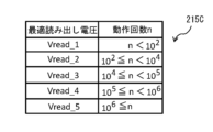
- the refresh information storage unit 215 stores, for example, an optimum read voltage table 215C as shown in FIG.
- the optimal read voltage table 215C defines the relationship between the above-described optimal read voltage and the number of operations n in a plurality of partitioned ranges.
- the memory control unit 212 acquires the range of the number of operations n corresponding to the derived optimum read voltage from the optimum read voltage table 215C.
- the memory control unit 212 acquires the refresh cycle Tr corresponding to the acquired range of the number of operations n from the refresh cycle table 215B. Even in this case, it is possible to more reliably prevent malfunctions, as in the above-described embodiment. Note that the method of deriving the number of operations n is not limited to the above.
- a voltage table 212A as shown in FIG. 20 may be provided in the memory controller 210.
- the memory controller 210 may be provided with an address conversion table 215A as shown in FIG. 21, for example.
- a read voltage Vread and a write voltage Vwrite are set for each section that collects a plurality of physical addresses.
- the write voltage Vwrite includes, for example, the above Vset and Vrset.
- Address conversion table 215A describes the number of operations n, refresh time t0, and refresh period Tr for each section.
- the memory cell array 223 is partitioned into multiple memory areas, and multiple physical addresses assigned to each memory area correspond to one section.
- the memory control unit 213 Upon receiving a read command from the host 10, the memory control unit 213 reads the read voltage set at the physical address specified by the command from the host 10 from the voltage table 212A. The memory control unit 213 generates a read request using the physical address and read voltage. The memory control unit 213 transmits the generated read request to the NVM 220 via the memory IF 214 .
- the memory control unit 212 Upon receiving a write command from the host 10, the memory control unit 212 reads the write voltage set at the physical address specified by the command from the host 10 from the voltage table 212A. The memory control unit 213 generates a write request using the physical address and the read write voltage. The memory control unit 213 transmits the generated write request together with the data received from the host 10 to the NVM 220 via the memory IF 214 .
- the memory control unit 213 Upon acquiring the refresh command from the refresh control unit 217, the memory control unit 213 reads the read voltage set at the physical address specified by the refresh command from the voltage table 212A. The memory control unit 213 generates a read request, which is one form of refresh request, using the physical address specified by the refresh command and the read voltage read. The memory control unit 213 transmits the generated read request to the NVM 220 via the memory IF 214 . That is, the memory control unit 213 controls the refresh operation for each memory area based on at least one of the number of times of writing and the number of times of reading for each memory area.
- the memory control unit 213 acquires the refresh command from the refresh control unit 217, the physical address specified by the refresh command is set from the voltage table 212A. Read the write voltage.
- the memory control unit 213 generates a write request, which is one form of refresh request, using the physical address specified by the refresh command and the read write voltage.
- the memory control unit 213 transmits the generated write request together with predetermined data to the NVM 220 via the memory IF 214 .
- the predetermined data is, for example, data in which all are "1" (that is, all memory elements ME included in the section corresponding to the physical address specified by the refresh command are in the low resistance state (LRS). data).
- the writing process by the array control unit 222 refreshes both the select element SE and the memory element ME.
- the memory control unit 213 writes the data held in the write data buffer of the buffer 224 to all the memory elements ME included in the section corresponding to the physical address specified by the refresh command. return.
- the present disclosure can have the following configurations.
- a nonvolatile memory cell array unit a memory controller that controls write and read operations for the nonvolatile memory cell array unit; the memory controller controls a refresh operation for the nonvolatile memory cell array unit using at least one of the write operation and the read operation; The memory controller sets the cycle of the refresh operation based on at least one of the number of writes and the number of reads to the nonvolatile memory cell array unit.
- the memory controller divides the nonvolatile memory cell array unit into a plurality of memory areas, and controls the refresh operation for each memory area based on at least one of the number of times of writing and the number of times of reading for each memory area.
- the nonvolatile memory cell array unit is a plurality of first wirings; a plurality of second wires; a memory cell array in which one memory cell is provided at each intersection of the plurality of first wirings and the plurality of second wirings;
- the memory cell has a storage element for recording 1-bit information according to the state of resistance value, and a selection element connected in series with the storage element,
- the memory controller controls a first refresh operation in which the refresh operation is performed only on the selected element, and a second refresh operation in which the refresh operation is performed on both the selected element and the storage element.
- the nonvolatile memory cell array unit is a plurality of first wirings; a plurality of second wires; a memory cell array in which one memory cell is provided at each intersection of the plurality of first wirings and the plurality of second wirings;
- the memory cell is composed of a single layer having information recording and information selection functions,
- the memory controller controls the refresh operation for the single layer.
- a memory control method comprising: setting a cycle of the refresh operation based on at least one of the number of times of writing and the number of times of reading to the nonvolatile memory cell array unit.
- the refresh operation for the nonvolatile memory cell array unit using at least one of the write operation and the read operation for the nonvolatile memory cell array unit is controlled.
- the refresh operation using the read operation is performed, the refresh operation is not performed in the high-resistance memory cells.
- the refresh operation using the write operation is performed, the refresh operation is performed on any memory cell. Therefore, it is possible to prevent malfunction.
- the refresh operation period is set based on at least one of the number of writes and the number of reads to the nonvolatile memory cell array unit.
Landscapes
- Dram (AREA)
- Techniques For Improving Reliability Of Storages (AREA)
- Read Only Memory (AREA)
- Semiconductor Memories (AREA)
Abstract
本開示の一側面に係るメモリ装置は、不揮発性メモリセルアレイユニットと、不揮発性メモリセルアレイユニットに対する書き込み動作および読み出し動作を制御するメモリコントローラとを備えている。メモリコントローラは、書き込み動作および読み出し動作のうち少なくとも一方の動作を利用して不揮発性メモリセルアレイユニットに対するリフレッシュ動作を制御する。メモリコントローラは、さらに、不揮発性メモリセルアレイユニットに対する書き込み回数および読み出し回数のうち少なくとも一方に基づいて、リフレッシュ動作の周期を設定する。
Description
本開示は、メモリ装置およびメモリ制御方法に関する。
データを不揮発に記憶することの可能なメモリシステムが知られている(例えば、特許文献1参照)。このようなメモリシステムでは、記憶素子および選択素子が直列に接続されたセル構造がメモリセルごとに設けられる。各メモリセルにおいては、アクセスしていない時間が長くなり過ぎると、動作電圧の変位により読み出し不良や書き込み不良が発生し得る。このような動作不良を防ぐために、リフレッシュ動作を行うことが考えられる。
特許文献1に記載の方法では、乱数発生器を用いたリフレッシュが行われる。しかし、特許文献1に記載の方法では、リフレッシュを行っていないメモリセルにおける動作不良を防ぐには確実性に欠けるという問題があった。従って、より確実に動作不良を防ぐことの可能なメモリ装置およびメモリ制御方法を提供することが望ましい。
本開示の一側面に係るメモリ装置は、不揮発性メモリセルアレイユニットと、不揮発性メモリセルアレイユニットに対する書き込み動作および読み出し動作を制御するメモリコントローラとを備えている。メモリコントローラは、書き込み動作および読み出し動作のうち少なくとも一方の動作を利用して不揮発性メモリセルアレイユニットに対するリフレッシュ動作を制御する。メモリコントローラは、さらに、不揮発性メモリセルアレイユニットに対する書き込み回数および読み出し回数のうち少なくとも一方に基づいて、リフレッシュ動作の周期を設定する。
本開示の一側面に係るメモリ制御方法は、以下の2つを含む。
(A)不揮発性メモリセルアレイユニットに対する書き込み動作および読み出し動作のうち少なくとも一方の動作を利用して不揮発性メモリセルアレイユニットに対するリフレッシュ動作を制御すること
(B)不揮発性メモリセルアレイユニットに対する書き込み回数および読み出し回数のうち少なくとも一方に基づいて、リフレッシュ動作の周期を設定すること
(A)不揮発性メモリセルアレイユニットに対する書き込み動作および読み出し動作のうち少なくとも一方の動作を利用して不揮発性メモリセルアレイユニットに対するリフレッシュ動作を制御すること
(B)不揮発性メモリセルアレイユニットに対する書き込み回数および読み出し回数のうち少なくとも一方に基づいて、リフレッシュ動作の周期を設定すること
本開示の一側面に係るメモリ装置およびメモリ制御方法では、不揮発性メモリセルアレイユニットに対する書き込み動作および読み出し動作のうち少なくとも一方の動作を利用した不揮発性メモリセルアレイユニットに対するリフレッシュ動作が制御される。ここで、読み出し動作を利用したリフレッシュ動作がなされたとき、高抵抗のメモリセルではリフレッシュ動作がなされない。しかし、時間の経過とともに動作電圧が上昇することによって動作不良が生じる場合には、高抵抗のメモリセルに対してリフレッシュ動作を行わなくても、読み出し不良が生じるおそれは無い。また、書き込み動作を利用したリフレッシュ動作がなされたときは、いずれのメモリセルに対してもリフレッシュ動作がなされる。従って、動作不良を防ぐことが可能である。また、本開示の一側面に係るメモリ装置およびメモリ制御方法では、不揮発性メモリセルアレイユニットに対する書き込み回数および読み出し回数のうち少なくとも一方に基づいて、リフレッシュ動作の周期が設定される。これにより、書き込み回数または読み出し回数に応じて動作電圧の変位の度合いが変わる場合であっても、動作不良が生じる前にリフレッシュ動作を行うことが可能となる。
以下、本開示を実施するための形態について、図面を参照して詳細に説明する。ただし、以下に説明する実施形態は、あくまでも例示であり、以下に明示しない種々の変形や技術の適用を排除する意図はない。本技術は、その趣旨を逸脱しない範囲で種々変形(例えば各実施形態を組み合わせる等)して実施することができる。また、以下の図面の記載において、同一又は類似の部分には同一又は類似の符号を付して表している。図面は模式的なものであり、必ずしも実際の寸法や比率等とは一致しない。図面相互間においても互いの寸法の関係や比率が異なる部分が含まれていることがある。
<1.実施の形態>
図1は、本開示の一実施の形態に係る情報処理システムの概略構成の一例を表す。この情報処理システムは、例えば、図1に示したように、ホスト10および不揮発性記憶装置20を備える。不揮発性記憶装置20は、例えば、図1に示したように、メモリコントローラ210および不揮発性メモリ(NVM:Non-Volatile Memory)セルアレイユニット(NVM220)を有する。
図1は、本開示の一実施の形態に係る情報処理システムの概略構成の一例を表す。この情報処理システムは、例えば、図1に示したように、ホスト10および不揮発性記憶装置20を備える。不揮発性記憶装置20は、例えば、図1に示したように、メモリコントローラ210および不揮発性メモリ(NVM:Non-Volatile Memory)セルアレイユニット(NVM220)を有する。
メモリコントローラ210は、ホスト10と通信し、ホスト10から書き込みコマンド又は読み出しコマンドを受信する。メモリコントローラ210は、受信したコマンドに基づき、NVM220への書き込み動作、又はNVM220からの読み出し動作を制御する。
メモリコントローラ210は、ホスト10から書き込みコマンドを受信した場合、ホスト10からさらに、書き込み用のデータを受信する。メモリコントローラ210は、NVM220に書き込み要求を発行して、ホスト10から受信したデータをNVM220に送信する。NVM220は、メモリコントローラ210から受信したデータを内部のメモリセルアレイ(図2参照)に書き込む。
メモリコントローラ210は、ホスト10から読み出しコマンドを受信した場合、NVM220に読み出し要求を発行して、NVM220に送信する。不揮発性メモリセルアレイユニット220は、読み出し要求に応じてメモリセルアレイからデータを読み出し、読み出したデータをメモリコントローラ210に送信する。メモリコントローラ210は、NVM220から受信したデータをホスト10に送信する。
図2は、メモリコントローラ210および不揮発性メモリセルアレイユニット220の機能ブロックの一例を表す。メモリコントローラ210は、例えば、図2に示したように、ホストインターフェース部(ホストIF)211、メモリ制御部212、メモリインターフェース部(メモリIF)213、タイマ214、リフレッシュ情報記憶部215およびリフレッシュ制御部216を有する。不揮発性メモリセルアレイユニット220は、例えば、図2に示したように、メモリインターフェース部(メモリIF)221、アレイ制御部222、メモリセルアレイ223およびバッファ224を有する。
メモリセルアレイ223は、例えば、複数のタイル223Aを有する。図3は、タイル223Aの概略構成の一例を表したものである。タイル223Aは、例えば、図3に示したように、複数のビット線BLと、複数のワード線WLと、複数のメモリセルMCとを有する。複数のメモリセルMCは、複数のビット線BLと複数のワード線WLとの交差部に1つずつ配置される。この構造は、いわゆるクロスポイント構造と呼ばれる。メモリセルMCは、書き込み可能な不揮発性のメモリである。メモリセルMCは、抵抗値の高低の状態により1ビットの情報を記録する記憶素子ME(Memory Element)と、記憶素子MEに直列に接続された選択素子SE(Selector Element)とを有する。
記憶素子MEは、例えば相変化メモリ材料であり、ゲルマニウム(Ge)アンチモン(Sb)テルル(Te)のカルコゲナイド合金で形成することができる。保持特性や動作電流の観点から種々の元素が添加されてもよい。また、記憶素子MEは、OxRAM(Oxide-based RAM)、CBRAM(Conductive Bridge RAM)などの抵抗変化型メモリ材料であってもよく、材料に限定されない。動作電圧が変位するドリフト現象が発生しないメモリ材料の場合は、動作電圧をドリフト現象発生前の電圧に戻すリフレッシュ動作は選択素子SEに適用され得る。
選択素子SEは、例えばオボニック閾値スイッチ(OTS:Ovonic Threshold Switch)である。選択素子SEは、例えば、テルル(Te)、セレン(Se)および硫黄(S)からなる群より選択された少なくとも1種以上のカルコゲン元素を含む材料にて形成することができる。また、選択素子SEは、アモルファス構造の安定化やリーク電流の低減を目的として、ホウ素(B)、アルミニウム(Al)、ガリウム(Ga)、インジウム(In)、炭素(C)、ゲルマニウム(Ge)、ヒ素(As)、ケイ素(Si)、酸素(O)および窒素(N)などを含んでもよい。選択素子SEの材料は、上述の材料に限定されるものではなく、ドリフト現象が発生する材料が適用され得る。
なお、メモリセルMCには、記憶素子MEと選択素子SEとの間に中間電極が設けられてもよい。記憶素子MEと選択素子SEとが互いに直接、接合されてもよい。逆に密着性や材料拡散の観点から、記憶素子MEと選択素子SEとの間に、接着層や拡散防止層などが設けられてもよい。また、メモリセルMCには、記憶素子MEおよび選択素子SEの代わりに、記憶素子ME(情報記録)および選択素子SE(情報選択)の機能を兼ね備えた単一の層が設けられてもよい。このような単一の層としては、例えば、オボニック閾値スイッチが挙げられる。例えば、オボニック閾値スイッチにおいて、動作電流や電圧印加方向によって発生した複数の閾値状態を記憶データとして用いることにより、記憶素子MEおよび選択素子SEの機能を単一の層で担うことが可能となる。
記憶素子MEは、例えば、相互に遷移可能な低抵抗状態(LRS)と高抵抗状態(HRS)のうちの1つの抵抗状態を有する。また一例としてLRSは第1値に対応し、HRSは第2値に対応する。第1値は“1”に対応し、第2値は“0”に対応する。あるいは、第1値は“0”に対応し、第2値は“1”に対応してもよい。本実施形態では、LRSは“1”に対応し、HRSは“0”に対応する場合を想定するが、これに限定されない。
図4は、記憶素子MEが低抵抗状態(LRS)および高抵抗状態(HRS)のときのメモリセルMCの電流電圧特性の例を表す。読出し電圧Vreadは記憶素子MEが低抵抗状態(LRS)のときの閾値電圧より高く、記憶素子MEが高抵抗状態(HRS)のときの閾値電圧より低く設定される。すなわち、読出し動作では、記憶素子MEが低抵抗の状態のときにのみオン状態になり選択素子SEがリフレッシュされる。
選択素子SEは、長時間オンにしないと、選択素子SEをオンするために必要な閾値電圧が上昇(ドリフトと呼ぶ)する。図5は選択素子SEのドリフト現象によるI-V特性の例を表したものである。ある動作(0min)から次の動作までに180°1時間経過すると、選択素子SEがオンするのに必要な閾値電圧が上昇することがわかる。さらに、0minから260°10分経過した場合には、180°1時間経過したときよりも閾値の上昇幅は大きく、温度によってドリフト現象が加速されることがわかる。ドリフト後に閾値以上の電圧が選択素子SEに印加されることにより、選択素子SEはオンする。選択素子SEがオンすると、ドリフトは解消される。これにより、ドリフトされた閾値電圧は、初期の値の電圧に戻る。
図6は、カルコゲナイド材料としてTeを含む選択素子SEにおいて85°1日の条件下でのドリフトによる閾値変動と動作回数の関係性を表す。図6では、100回動作済の選択素子SEにおける閾値変動量を1として閾値変動量が規格化されている。図6によれば、動作回数が多くなるとドリフトによる閾値変動が小さくなる傾向があることがわかる。すなわち、100回動作させた選択素子SEをリフレッシュする周期に対して、100万回動作させた選択素子SEをリフレッシュする周期を長く設定することが可能である。このようにした場合、動作回数が多い選択素子SEに対してはリフレッシュ頻度を低減させることができ、消費電力の低減が期待される。
ドリフトによる閾値変動は必ずしも一定とは限らない。図7は、GeAsSeで構成された選択素子SEにおいて85°1日の条件下でのドリフトによる閾値変動と動作回数の関係性を表す。図7では、100回動作済の選択素子SEにおける閾値変動量を1として閾値変動量が規格化されている。図7によれば、動作回数が多くなるとドリフトによる閾値変動が大きくなる傾向があることがわかる。すなわち、100万回動作させた選択素子SEをリフレッシュする周期に対して、100回動作させた選択素子SEをリフレッシュする周期を長く設定することが可能である。このようにした場合、動作回数が少ない選択素子SEに対してはリフレッシュ頻度を低減させることができ、消費電力の低減が期待される。
図8は、GeAsSeに対し上述したような添加元素をドープした選択素子SEにおいて、85°1日の条件下でのドリフトによる閾値変動と動作回数の関係性を表す。図8では、100回動作済の選択素子SEにおける閾値変動量を1として閾値変動量が規格化されている。図8によれば、動作回数が多くなるとドリフトによる閾値変動が小さくなる傾向があることがわかる。すなわち、100回動作させた選択素子SEをリフレッシュする周期に対して、100万回動作させた選択素子SEをリフレッシュする周期を長く設定することが可能である。このようにした場合、動作回数が多い選択素子SEに対してはリフレッシュ頻度を低減させることができ、消費電力の低減が期待される。
メモリセルMCからデータを読み出す方法の一例について説明する。選択したメモリセルMCに接続されたワード線WLとビット線BLにそれぞれ-Vread/2、Vread/2の電圧のパルスが印加される。選択したメモリセルMCに所定の読み出し電圧Vread(=Vread/2-(-Vread/2)の読み出しパルスが印加される。メモリセルMCに流れた電流に基づき、記憶素子MEの抵抗状態が、LRS及びHRSのいずれであるかが判別される。選択素子SEがオンする場合、メモリセルMCに電流が流れる。この場合、記憶素子MEの抵抗状態はLRSであるとして、“1”のデータが読み出される。選択素子SEがオンしない場合、メモリセルMCに電流が流れない。この場合、記憶素子MEの抵抗状態はHRSであるとして、“0”のデータが読み出される。
ドリフトの発生により閾値電圧が所定の読み出し電圧より大きくなっている場合、記憶素子MEがLRSであっても、所定の読み出し電圧の印加により選択素子SEはオンしない。このため、記憶素子MEの抵抗状態がLRSであっても、LRSの判別に必要な電流が流れない。この結果、記憶素子MEの状態はHRSと誤判別されてしまう。すなわち、実際にはメモリセルMCには“1”のデータが格納されているものの、“0”のデータが格納されていると判断される。
メモリセルMCにデータを書き込む方法の一例について説明する。メモリセルMCに“1”のデータを書き込む場合(セットと呼ぶ)、選択したメモリセルMCに接続されたワード線WLとビット線BLにそれぞれ-Vset/2、Vset/2の電圧のパルスが印加される。選択したメモリセルMCに所定のセット電圧Vset(=Vset/2-(-Vset/2)のセットパルスが印加される。記憶素子MEの抵抗状態がHRSの場合は、LRSに遷移する。これにより、メモリセルMCに“1”のデータが書き込まれる。
メモリセルMCに“0”のデータを書き込む場合(リセットと呼ぶ)、選択したメモリセルMCに接続されたワード線WLとビット線BLにそれぞれ-Vreset/2、Vreset/2で電圧のパルスが印加される。選択したメモリセルMCに所定のリセット電圧Vreset(=Vreset/2-(-Vreset/2))のリセットパルスが印加される。なお、メモリセルMCの材料によっては、リセットパルスの電圧の方向は、セットパルスとは逆方向となっていてもよい。記憶素子MEの抵抗状態がLRSの場合は、HRSに遷移する。これにより、メモリセルMCに“0”のデータが書き込まれる。
選択素子SEが所定の読み出し電圧Vreadでオンするように所定の読み出し電圧Vread以下に閾値電圧を収めるためには、定期的に選択素子SEをオンにし、ドリフトを解消する必要がある。選択素子SEをオンにすることで、閾値電圧は初期の値の電圧に戻る。これによりドリフトは解消される。
次に、NVM220における他の構成について説明する。
メモリIF221は、メモリコントローラ210と通信する。メモリIF221は、メモリコントローラ210から要求を受信した場合、受信した要求をアレイ制御部222に提供する。要求の種類として、読み出し要求、書き込み要求、リフレッシュ要求などがある。メモリIF221は、メモリコントローラ210から書き込み用のデータを受信した場合、当該データをバッファ224のライトデータバッファに書き込む。
アレイ制御部222は、メモリIF221を介して、メモリコントローラ210から要求を受信する。アレイ制御部222は、受信した要求の種類に応じた動作を行う。アレイ制御部222は、メモリセルアレイ223のワード線駆動部およびビット線駆動部を制御する。アレイ制御部222は、メモリセルアレイ223におけるメモリセルMCにアクセス(読み出し、セット、リセット)する場合、アクセス対象のメモリセルMCに接続されたワード線WLとビット線BLを選択し、選択したワード線WL及びビット線BLに、必要な電圧を印加する。
アレイ制御部222は、読み出し要求を実行する場合、選択したワード線WL及びビット線BLに対して読み出しパルスを電圧として印加する。これにより、該当するメモリセルMCからデータの読み出しを行う。この読み出しを、読み出し要求で指定された物理アドレスに属する複数のメモリセルMCについて行う。複数のメモリセルMCから読み出されたデータは、バッファ224のリードデータバッファに保持される。アレイ制御部222は、リードデータバッファに保持されたデータを、メモリIF221を介して、メモリコントローラ210に送信する。
アレイ制御部222は、書き込み要求を実行する場合、まずは書き込み要求で指定された物理アドレスに属する複数のメモリセルMCからデータを読み出し、バッファ224のリードデータバッファに保持する。アレイ制御部222は、リードデータバッファに保持されたデータと、ライトデータバッファに保持されたデータとを比較する。アレイ制御部222は、ライトデータバッファに保持された値が“1”であり、リードデータバッファに保持された値が“0”であるビットに対応するメモリセルMCには、“1”を書き込む(セットする)。すなわち、アレイ制御部222は、そのようなメモリセルMCに接続されたワード線WL及びビット線BLに対しては、セットパルスを電圧として印加する。アレイ制御部222は、ライトデータバッファに保持された値が“0”であり、リードデータバッファに保持された値が“1”であるビットに対応するメモリセルMCには、“0”を書き込む(リセットする)。すなわち、アレイ制御部222は、そのようなメモリセルMCに接続されたワード線WL及びビット線BLに対しては、リセットパルスを電圧として印加する。アレイ制御部222は、ライトデータバッファに保持された値と、リードデータバッファに保持された値とが互いに同じ場合は、何も書き込みを行わない。
なお、上記は一例であり、アレイ制御部222は、書き込み要求を実行する場合に書き込み要求で指定された物理アドレスに属する複数のメモリセルMCからデータを読み出すことなく、書き込みを実施するようにしてもよい。その場合、書き込み回数は増加するが、データを読み出し保持されたデータと比較する時間が短縮される。
次に、メモリコントローラ210の構成について説明する。
ホストIF211は、ホスト10からコマンド(書き込みコマンド又は読出しコマンド)を受信する。ホストIF211は、受信したコマンドをメモリ制御部212に送信する。また、ホストIF211は、ホスト10から書き込みコマンドで書き込み指示されるデータを受信し、受信したデータを、書き込みコマンドに関連づけてメモリ制御部212に送信する。ホストIF211は、NVM220から読み出されたデータを受信し、受信したデータをホスト10に送信する。
メモリ制御部212は、ホスト10から書き込みコマンドを受信すると、書き込みコマンドに含まれる物理アドレスを用いて、書き込み要求を生成する。メモリ制御部212は、生成した書き込み要求を、ホスト10から受信したデータとともに、メモリIF213を介してNVM220に送信する。メモリ制御部212は、ホスト10から読み出しコマンドを受信すると、読み出しコマンドに含まれる物理アドレスを用いて、読み出し要求を生成する。メモリ制御部212は、生成した読み出し要求を、メモリIF213を介してNVM220に送信する。
リフレッシュ情報記憶部215は、例えば、図9、図10に示したように、リフレッシュ動作テーブル215Aおよびリフレッシュ周期テーブル215Bを有する。
リフレッシュ動作テーブル215Aには、例えば、図9に示したように、動作回数n、リフレッシュ時刻t0およびリフレッシュ周期Trが記述されている。リフレッシュ時刻t0は、例えば、電源遮断などの異常時に、リフレッシュの周期を補正するための参照データとして使用され得る。
動作回数nは、メモリセルアレイ223に対する書き込み回数および読み出し回数の合計値(累積値)である。リフレッシュ動作テーブル215Aにおいて、動作回数nは、メモリセルアレイ223に対して、書き込み処理や読み出し処理が行われる度に1つ増える。リフレッシュ時刻t0は、メモリセルアレイ223に対してリフレッシュ動作が行われたときの時刻である。リフレッシュ時刻t0は、タイマ214から得られる。リフレッシュ周期Trは、メモリセルアレイ223に対して行われるリフレッシュ動作の周期である。リフレッシュ周期Trは、リフレッシュ時刻t0から、次回のリフレッシュ動作が行わるまでの期間である。
リフレッシュ周期テーブル215Bには、例えば、図10に示したように、動作回数nと、リフレッシュ周期Trとの対応関係が記述されている。リフレッシュ周期テーブル215Bにおいて、動作回数nは、複数の範囲に区画されており、区画された範囲ごとに、リフレッシュ周期Trが設定される。
なお、リフレッシュ動作テーブル215Aにおいて、例えば、図11に示したように、動作回数nが、読み出し回数nrと書き込み回数nwとに分けて記述されていてもよい。さらに、リフレッシュ周期テーブル215Bにおいて、読み出し回数nrおよび書き込み回数nwの少なくとも一方に対して重み付けがなされていてもよい。
例えば、図12に示したように、読み出し回数nrに対してα(0<α<1)が乗算されるようになっていてもよい。読み出し時に、記憶素子MEが高抵抗状態(HRS)となっている場合には、高抵抗状態(HRS)の記憶素子MEに接続された選択素子SEはリフレッシュされない。また、読み出し動作と書き込み動作でメモリセルMCへの負荷が異なることがある。その場合には、読み出し回数に対してαを乗算し、読み出し回数を控えめに評価することが、読み出し不良防止の観点から重要である。
なお、リフレッシュ動作テーブル215Aにおいて、動作回数nが読み出し回数nrのみ、または、書き込み回数nwのみであってもよい。例えば、本システムの用途の関係から、メモリセルMCからの読み出しがメモリセルMCへの書き込みと比べてあまり多くないことがわかっている場合、動作回数nが書き込み回数nwのみであってもよい。また、例えば、本システムの用途の関係から、メモリセルMCへの書き込みがメモリセルMCからの読み出しと比べてあまり多くないことがわかっている場合、動作回数nが読み出し回数nrのみであってもよい。
メモリ制御部212は、ホスト10から制御コマンド(読み出しコマンドもしくは書き込みコマンド)を取得する(図13、ステップS101)。すると、メモリ制御部212は、受信した制御コマンドをリフレッシュ制御部216に出力する(図13、ステップS102)。リフレッシュ制御部216は、制御コマンドをメモリ制御部212から取得すると(図13、ステップS103)、動作回数nを更新する(1つ増やす)(図13、ステップS104)。このとき、リフレッシュ制御部216は、必要に応じて、読み出し回数nrおよび書き込み回数nwの少なくとも一方に対して重み付けを行った上で、動作回数nを更新してもよい。
リフレッシュ制御部216は、リフレッシュ周期テーブル215Bから、更新後の動作回数nが含まれる範囲に対応するリフレッシュ周期Trを取得する(図13、ステップS105)。リフレッシュ制御部216は、取得したリフレッシュ周期Trを、新たなリフレッシュ周期Trとしてリフレッシュ動作テーブル215Aに上書きする(格納する)(図13、ステップS106)。つまり、リフレッシュ制御部216は、読み出し回数nrおよび書き込み回数nwの少なくとも一方に基づいて、リフレッシュ動作の周期(リフレッシュ周期Tr)を設定する。
リフレッシュ制御部216は、タイマ214からリフレッシュトリガが出力される周期を更新する場合(ステップS201;Y)、リフレッシュ動作テーブル215Aからリフレッシュ周期Trを読み出す(ステップS202)。リフレッシュ制御部216は、読み出したリフレッシュ周期Trをタイマ214の内部メモリに設定する(書き込む)ことによって、タイマ214からリフレッシュトリガが出力される周期を更新する(ステップS203)。リフレッシュ制御部216は、タイマ214からリフレッシュトリガが出力される周期を更新しない場合(ステップS201;N)、上記ステップS202,203を実行しない。リフレッシュ制御部216は、タイマ214から出力(リフレッシュトリガ)を受信すると(ステップS204)、リフレッシュコマンドを生成し、メモリ制御部212に出力する(ステップS205)。
タイマ214は、内臓メモリに設定されたリフレッシュ周期Trで、リフレッシュトリガをリフレッシュ制御部216に出力する。内臓メモリに設定されたリフレッシュ周期Trは、リフレッシュ制御部216から新たなリフレッシュ周期Trが設定される度に更新される。
メモリ制御部212は、リフレッシュ制御部216からリフレッシュコマンドを取得すると、リフレッシュ要求の一形態である読み出し要求を生成する。つまり、本実施の形態では、メモリ制御部212は、読み出し動作を利用してリフレッシュ動作を制御する。メモリ制御部212は、生成した読み出し要求を、メモリIF213を介してNVM220に送信する。
図15は、リフレッシュ周期の変遷について説明する図を表す。図15に記載の「Refl」はリフレッシュ制御(リフレッシュコマンドの入力に応じた処理)が行われていることを意味する。図15では、リフレッシュ周期TrがTaからTbに変化し、その後、Tcに変化する様子が示されている。
メモリ制御部212は、例えば、メモリセルアレイ223に対して、リフレッシュ周期Taでリフレッシュ制御を行い、その後、リフレッシュ周期TrをTaからTbに変化させ、さらに、TbからTcに変化させる。メモリ制御部212は、図15に記載の各「Refl」において、メモリセルアレイ223内の複数のメモリセルMCに対して順次、リフレッシュ制御を行う。メモリコントローラ210がレジスタを有している場合に、メモリ制御部212は、そのレジスタに設定したアドレス番号を順次更新していくことにより、メモリセルアレイ223内の複数のメモリセルMCを順次、選択し、リフレッシュ制御を行う。
図15に記載の各「Refl」において、メモリ制御部212によるリフレッシュ制御が行われるに伴って、低抵抗状態(LRS)の記憶素子MEに接続された選択素子SEはリフレッシュされ、高抵抗状態(HRS)の記憶素子MEに接続された選択素子SEはリフレッシュされない。リフレッシュされた選択素子SEでは動作電圧がドリフト現象発生前の電圧に戻る。一方、リフレッシュされなかった選択素子SEでは動作電圧がドリフト現象発生後の電圧のままとなっている。しかし、リフレッシュされなかった選択素子SEには高抵抗状態(HRS)の記憶素子MEが接続されているので、選択素子SEの動作電圧が時間の経過とともに上昇したとしても、このメモリセルMCの読み出し結果は、HRSに対応する値のままである。選択素子SEの動作電圧が時間の経過とともに上昇した場合、このメモリセルMCの読み出し結果がLRSに対応する値になる可能性はむしろ低下する。従って、リフレッシュされなかった選択素子SEを含むメモリセルMCにおいても、安定的な読み出しが可能である。
図15に記載の各「Refl」では、メモリセルアレイ223から読み出されたデータはメモリコントローラ210やホスト10に出力されなくてもよい。図15に記載の各「Refl」で、メモリセルアレイ223から読み出されたデータは、メモリコントローラ210やホスト10にとっては必要のないデータであり、メモリコントローラ210やホスト10に送信する必要がないからである。従って、図15に記載の各「Refl」において、リフレッシュ動作が終了した段階で、アレイ制御部222がバッファ224のデータの、メモリコントローラ210への転送を実行せず、バッファ224のデータを削除することが好ましい。このようにした場合には、ホスト10とメモリコントローラ210間のデータ通信を他の用途に使うことができ、ホスト10とメモリコントローラ210間のデータ通信が高速化され得る。
なお、メモリ制御部212は、例えば、図16に示したように、メモリセルアレイ223において、リフレッシュ周期Trごとに複数回ずつ(例えば2回ずつ)、リフレッシュ制御を行ってもよい。このとき、メモリ制御部212は、リフレッシュ周期Trにおいて、後に行うリフレッシュ制御における読み出し電圧の大きさを、前に行うリフレッシュ制御における読み出し電圧の大きさよりも所定の大きさだけ大きくしてもよい。そのようにした場合には、閾値電圧のばらつきに起因して1回目のリフレッシュ制御において選択素子SEをオンさせることができなかった場合であっても、2回目以降のリフレッシュ制御において選択素子SEをオンさせることが可能となる。
ところで、ホスト10からの書き込みコマンドまたは読み出しコマンドの入力タイミングと、リフレッシュ制御部216からのリフレッシュコマンドの入力タイミングとが互いに競合してしまうことが考えられる。この場合、メモリ制御部212は、書き込みコマンドまたは読み出しコマンドを、リフレッシュコマンドよりも優先して処理してもよいし、その逆に、リフレッシュコマンドを書き込みコマンドまたは読み出しコマンドよりも優先して処理してもよい。
例えば、書き込みコマンドまたは読み出しコマンドが何度も繰り返し、リフレッシュコマンドよりも優先して処理された場合、リフレッシュコマンドが周期的に処理されなくなり、動作不良が生じてしまう可能性がある。その場合、メモリ制御部212は、書き込みコマンドまたは読み出しコマンドがリフレッシュコマンドよりも優先して処理された回数が所定の回数を超えた場合に、リフレッシュコマンドを書き込みコマンドまたは読み出しコマンドよりも優先して処理するようにしてもよい。
また、不揮発性記憶装置20が、複数のNVM220を有しており、1つのメモリコントローラ210が複数のNVM220に対する書き込み、読み出しを制御するようになっていてもよい。この場合、メモリコントローラ210は、例えば、NVM220ごとに1つずつ割り当てられた複数のレジスタを有し、各レジスタに設定したアドレス番号を順次更新することにより、各NVM220に対して、同時にリフレッシュ制御を行ってもよい。
ところで、不揮発性記憶装置20が搭載されたシステムがスタンバイ状態にあるとき、各メモリセルMCへのアクセス頻度が低下し、動作不良を引き起こす可能性がある。そこで、メモリ制御部212は、例えば、不揮発性記憶装置20が搭載されたシステムがスタンバイ状態にあるときに、リフレッシュ制御を行うようにしてもよい。なお、メモリ制御部212は、不揮発性記憶装置20が搭載されたシステムの電源がオンされたときに、リフレッシュ制御を行うようにしてもよい。また、メモリ制御部212は、不揮発性記憶装置20が搭載されたシステムにおいてリセット信号が入力されたときに、リフレッシュ制御を行うようにしてもよい。
また、上記実施の形態では、リフレッシュ対象が選択素子SEとなっていた。そのため、上記実施の形態では、メモリ制御部212は、読み出し動作を利用してリフレッシュ動作を制御していた。しかし、上記実施の形態において、記憶素子MEが、ドリフト現象が発生するメモリ材料で形成されている場合(記憶素子MEが例えば相変化メモリの場合)には、リフレッシュ対象が選択素子SEおよび記憶素子MEとなっていてもよい。相変化メモリでは、動作電流やパルス幅を制御することで低抵抗状態と高抵抗状態とをそれぞれ作り出すことが可能である。この場合、メモリ制御部212は、例えば、図17に示したように、書き込み動作を利用してリフレッシュ動作を制御する。
具体的には、メモリ制御部212は、リフレッシュ制御部216からリフレッシュコマンドを取得すると、リフレッシュ要求の一形態である書き込み要求を生成する。メモリ制御部212は、生成した書き込み要求を、所定のデータとともに、メモリIF213を介してNVM220に送信する。ここで、所定のデータとは、例えば、全てが“1”のデータ(つまり、全ての記憶素子MEが低抵抗状態(LRS)となるデータ)である。その結果、アレイ制御部222による書き込み処理により、選択素子SEおよび記憶素子MEの双方がリフレッシュされる。メモリ制御部212は、このリフレッシュを行った後、バッファ224のライトデータバッファに保持しておいたデータを全ての記憶素子MEに書き戻す。
なお、アレイ制御部222は、リフレッシュ要求の一形態である書き込み要求を実行する場合に、まずはこの書き込み要求で指定された物理アドレスに属する複数のメモリセルMCからデータを読み出し、バッファ224のリードデータバッファに保持する。このとき、リードデータバッファに保持された値が“1”となっている場合(つまり、記憶素子MEが低抵抗状態となっている場合)、読み出しを行った時点で、低抵抗状態の記憶素子MEに接続された選択素子SEはリフレッシュされている。従って、アレイ制御部222は、ライトデータバッファに保持された値が“1”であり、リードデータバッファに保持された値が“1”であるビットに対応するメモリセルMCには、書き込みを行わなくてもよい(リフレッシュを行わなくてもよい)。
また、記憶素子MEが、ドリフト現象が発生するメモリ材料で形成されていない場合であっても、メモリ制御部212は、書き込み動作を利用してリフレッシュ動作を制御してもよい。
また、メモリ制御部212は、例えば、図18に示したように、読み出し動作を利用してリフレッシュ動作を制御するとともに、書き込み動作を利用してリフレッシュ動作を制御してもよい。このとき、メモリ制御部212は、メモリセルアレイ223に対して、読み出し動作を利用したリフレッシュ動作の制御と、書き込み動作を利用したリフレッシュ動作の制御とを交互に行ってもよい。また、メモリ制御部212は、メモリセルアレイ223に対して、例えば、図18に示したように、読み出し動作を利用したリフレッシュ動作の制御周期と、書き込み動作を利用したリフレッシュ動作の制御周期とを互いに異ならせてもよい。書き込み動作のリフレッシュはメモリセルに格納されているデータに依存せずにリフレッシュできるため、読み出し動作によるリフレッシュと書き込み動作のリフレッシュのタイミングが重なった場合、書き込み動作によるリフレッシュのみ実施させるようにするのが好ましい。なお、図18には、書き込み動作を利用したリフレッシュ動作の制御周期が、読み出し動作を利用したリフレッシュ動作の制御周期の4倍になっている場合が例示されている。このようにした場合には、上記実施の形態の場合と比べて、より確実に動作不良を防ぐことができる。
また、上記実施の形態において、リフレッシュ周期Trが、動作回数nに応じた選択素子SEの特性から決定されてもよい。具体的には、メモリ制御部212は、読み出し電圧が少しずつ異なる複数の読み出し要求を生成し、NVM220に送信する。その結果、メモリ制御部212は、複数の読み出し要求によって得られた複数のデータの中で最もエラーの少ないデータに対応する読出し要求を選択し、選択した読出し要求に含まれる読み出し電圧を、最適読み出し電圧とする。
リフレッシュ情報記憶部215には、例えば、図19に示したように、最適読み出し電圧テーブル215Cが格納されている。最適読み出し電圧テーブル215Cには、上述の最適読み出し電圧と、区画された複数の範囲の動作回数nとの関係が規定されている。メモリ制御部212は、最適読み出し電圧テーブル215Cから、導出した最適読み出し電圧に対応する、動作回数nの範囲を取得する。メモリ制御部212は、リフレッシュ周期テーブル215Bから、取得した動作回数nの範囲に対応するリフレッシュ周期Trを取得する。このようにした場合であっても、上記実施の形態と同様、より確実に動作不良を防ぐことができる。なお、動作回数nの導出方法については、上記に限定されるものではない。
また、上記実施の形態において、例えば、図20に示したような電圧テーブル212Aがメモリコントローラ210に設けられていてもよい。さらに、上記実施の形態において、例えば、図21に示したようなアドレス変換テーブル215Aがメモリコントローラ210に設けられていてもよい。電圧テーブル212Aには、複数の物理アドレスをまとめた1つのセクションごとに、読み出し電圧Vreadおよび書き込み電圧Vwriteが設定されている。書き込み電圧Vwriteには、例えば、上述のVsetやVrsetが含まれる。アドレス変換テーブル215Aには、セクションごとに、動作回数n、リフレッシュ時刻t0およびリフレッシュ周期Trが記述されている。ここで、メモリセルアレイ223が複数のメモリ領域に区画され、メモリ領域ごとに割り当てられた複数の物理アドレスが、1つのセクションに相当する。
メモリ制御部213は、ホスト10から読み出しコマンドを受信すると、電圧テーブル212Aから、ホスト10からのコマンドで指定された物理アドレスに設定された読み出し電圧を読み出す。メモリ制御部213は、物理アドレスと、読み出した読み出し電圧とを用いて、読み出し要求を生成する。メモリ制御部213は、生成した読み出し要求を、メモリIF214を介してNVM220に送信する。
メモリ制御部212は、ホスト10から書き込みコマンドを受信すると、電圧テーブル212Aから、ホスト10からのコマンドで指定された物理アドレスに設定された書き込み電圧を読み出す。メモリ制御部213は、物理アドレスと、読み出した書き込み電圧とを用いて、書き込み要求を生成する。メモリ制御部213は、生成した書き込み要求を、ホスト10から受信したデータとともに、メモリIF214を介してNVM220に送信する。
メモリ制御部213は、リフレッシュ制御部217からリフレッシュコマンドを取得すると、電圧テーブル212Aから、リフレッシュコマンドで指定された物理アドレスに設定された読み出し電圧を読み出す。メモリ制御部213は、リフレッシュコマンドで指定された物理アドレスと、読み出した読み出し電圧とを用いて、リフレッシュ要求の一形態である読み出し要求を生成する。メモリ制御部213は、生成した読み出し要求を、メモリIF214を介してNVM220に送信する。つまり、メモリ制御部213は、メモリ領域ごとの書き込み回数および読み出し回数のうち少なくとも一方に基づいて、リフレッシュ動作をメモリ領域ごとに制御する。
リフレッシュ対象が選択素子SEおよび記憶素子MEとなっている場合、メモリ制御部213は、リフレッシュ制御部217からリフレッシュコマンドを取得すると、電圧テーブル212Aから、リフレッシュコマンドで指定された物理アドレスに設定された書き込み電圧を読み出す。メモリ制御部213は、リフレッシュコマンドで指定された物理アドレスと、読み出した書き込み電圧とを用いて、リフレッシュ要求の一形態である書き込み要求を生成する。メモリ制御部213は、生成した書き込み要求を、所定のデータとともに、メモリIF214を介してNVM220に送信する。ここで、所定のデータとは、例えば、全てが“1”のデータ(つまり、リフレッシュコマンドで指定された物理アドレスに対応するセクションに含まれる全ての記憶素子MEが低抵抗状態(LRS)となるデータ)である。その結果、アレイ制御部222による書き込み処理により、選択素子SEおよび記憶素子MEの双方がリフレッシュされる。メモリ制御部213は、このリフレッシュを行った後、バッファ224のライトデータバッファに保持しておいたデータを、リフレッシュコマンドで指定された物理アドレスに対応するセクションに含まれる全ての記憶素子MEに書き戻す。
このように、セクションごとに書き込み電圧や読み出し電圧を設定することにより、セクションごとの動作回数nに応じたきめ細かなリフレッシュ制御を行うことができる。
以上、実施の形態を挙げて本技術を説明したが、本開示は上記実施の形態に限定されるものではなく、種々変形が可能である。なお、本明細書中に記載された効果は、あくまで例示である。本開示の効果は、本明細書中に記載された効果に限定されるものではない。本開示が、本明細書中に記載された効果以外の効果を持っていてもよい。
また、例えば、本開示は以下のような構成を取ることができる。
(1)
不揮発性メモリセルアレイユニットと、
前記不揮発性メモリセルアレイユニットに対する書き込み動作および読み出し動作を制御するメモリコントローラと
を備え、
前記メモリコントローラは、前記書き込み動作および前記読み出し動作のうち少なくとも一方の動作を利用して前記不揮発性メモリセルアレイユニットに対するリフレッシュ動作を制御し、
前記メモリコントローラは、前記不揮発性メモリセルアレイユニットに対する書き込み回数および読み出し回数のうち少なくとも一方に基づいて、前記リフレッシュ動作の周期を設定する
メモリ装置。
(2)
前記メモリコントローラは、前記不揮発性メモリセルアレイユニットを複数のメモリ領域に区画し、前記メモリ領域ごとの前記書き込み回数および前記読み出し回数のうち少なくとも一方に基づいて、前記リフレッシュ動作を前記メモリ領域ごとに制御する
(1)に記載のメモリ装置。
(3)
前記不揮発性メモリセルアレイユニットは、
複数の第1の配線と、
複数の第2の配線と、
メモリセルが前記複数の第1の配線と前記複数の第2の配線との交点に1つずつ設けられたメモリセルアレイと
を有し、
前記メモリセルは、抵抗値の高低の状態により1ビットの情報を記録する記憶素子と、前記記憶素子に直列に接続された選択素子とを有し、
前記メモリコントローラは、前記リフレッシュ動作を前記選択素子に対してだけ行う第1リフレッシュ動作の制御と、前記リフレッシュ動作を前記選択素子におよび前記記憶素子の双方に対して行う第2リフレッシュ動作の制御とを行う
(1)または(2)に記載のメモリ装置。
(4)
前記第1リフレッシュ動作の周期と、前記第2リフレッシュ動作の周期とは、互いに異なっている
(3)に記載のメモリ装置。
(5)
前記不揮発性メモリセルアレイユニットは、
複数の第1の配線と、
複数の第2の配線と、
メモリセルが前記複数の第1の配線と前記複数の第2の配線との交点に1つずつ設けられたメモリセルアレイと
を有し、
前記メモリセルは、情報記録および情報選択の機能を兼ね備えた単一の層によって構成され、
前記メモリコントローラは、前記リフレッシュ動作の制御を前記単一の層に対して行う
(1)または(2)に記載のメモリ装置。
(6)
不揮発性メモリセルアレイユニットに対する書き込み動作および読み出し動作のうち少なくとも一方の動作を利用して前記不揮発性メモリセルアレイユニットに対するリフレッシュ動作を制御することと、
前記不揮発性メモリセルアレイユニットに対する書き込み回数および読み出し回数のうち少なくとも一方に基づいて、前記リフレッシュ動作の周期を設定することと
を含む
メモリ制御方法。
(1)
不揮発性メモリセルアレイユニットと、
前記不揮発性メモリセルアレイユニットに対する書き込み動作および読み出し動作を制御するメモリコントローラと
を備え、
前記メモリコントローラは、前記書き込み動作および前記読み出し動作のうち少なくとも一方の動作を利用して前記不揮発性メモリセルアレイユニットに対するリフレッシュ動作を制御し、
前記メモリコントローラは、前記不揮発性メモリセルアレイユニットに対する書き込み回数および読み出し回数のうち少なくとも一方に基づいて、前記リフレッシュ動作の周期を設定する
メモリ装置。
(2)
前記メモリコントローラは、前記不揮発性メモリセルアレイユニットを複数のメモリ領域に区画し、前記メモリ領域ごとの前記書き込み回数および前記読み出し回数のうち少なくとも一方に基づいて、前記リフレッシュ動作を前記メモリ領域ごとに制御する
(1)に記載のメモリ装置。
(3)
前記不揮発性メモリセルアレイユニットは、
複数の第1の配線と、
複数の第2の配線と、
メモリセルが前記複数の第1の配線と前記複数の第2の配線との交点に1つずつ設けられたメモリセルアレイと
を有し、
前記メモリセルは、抵抗値の高低の状態により1ビットの情報を記録する記憶素子と、前記記憶素子に直列に接続された選択素子とを有し、
前記メモリコントローラは、前記リフレッシュ動作を前記選択素子に対してだけ行う第1リフレッシュ動作の制御と、前記リフレッシュ動作を前記選択素子におよび前記記憶素子の双方に対して行う第2リフレッシュ動作の制御とを行う
(1)または(2)に記載のメモリ装置。
(4)
前記第1リフレッシュ動作の周期と、前記第2リフレッシュ動作の周期とは、互いに異なっている
(3)に記載のメモリ装置。
(5)
前記不揮発性メモリセルアレイユニットは、
複数の第1の配線と、
複数の第2の配線と、
メモリセルが前記複数の第1の配線と前記複数の第2の配線との交点に1つずつ設けられたメモリセルアレイと
を有し、
前記メモリセルは、情報記録および情報選択の機能を兼ね備えた単一の層によって構成され、
前記メモリコントローラは、前記リフレッシュ動作の制御を前記単一の層に対して行う
(1)または(2)に記載のメモリ装置。
(6)
不揮発性メモリセルアレイユニットに対する書き込み動作および読み出し動作のうち少なくとも一方の動作を利用して前記不揮発性メモリセルアレイユニットに対するリフレッシュ動作を制御することと、
前記不揮発性メモリセルアレイユニットに対する書き込み回数および読み出し回数のうち少なくとも一方に基づいて、前記リフレッシュ動作の周期を設定することと
を含む
メモリ制御方法。
本開示の一側面に係るメモリ装置およびメモリ制御方法では、不揮発性メモリセルアレイユニットに対する書き込み動作および読み出し動作のうち少なくとも一方の動作を利用した不揮発性メモリセルアレイユニットに対するリフレッシュ動作が制御される。ここで、読み出し動作を利用したリフレッシュ動作がなされたとき、高抵抗のメモリセルではリフレッシュ動作がなされない。しかし、時間の経過とともに動作電圧が上昇することによって動作不良が生じる場合には、高抵抗のメモリセルに対してリフレッシュ動作を行わなくても、読み出し不良が生じるおそれは無い。また、書き込み動作を利用したリフレッシュ動作がなされたときは、いずれのメモリセルに対してもリフレッシュ動作がなされる。従って、動作不良を防ぐことが可能である。また、本開示の一側面に係るメモリ装置およびメモリ制御方法では、不揮発性メモリセルアレイユニットに対する書き込み回数および読み出し回数のうち少なくとも一方に基づいて、リフレッシュ動作の周期が設定される。これにより、書き込み回数または読み出し回数に応じて動作電圧の変位の度合いが変わる場合であっても、動作不良が生じる前にリフレッシュ動作を行うことが可能となる。従って、本開示では、より確実に動作不良を防ぐことができる。なお、本開示の効果は、ここに記載された効果に必ずしも限定されず、本明細書中に記載されたいずれの効果であってもよい。
本出願は、日本国特許庁において2022年2月25日に出願された日本特許出願番号第2022-028507号を基礎として優先権を主張するものであり、この出願のすべての内容を参照によって本出願に援用する。
当業者であれば、設計上の要件や他の要因に応じて、種々の修正、コンビネーション、サブコンビネーション、および変更を想到し得るが、それらは添付の請求の範囲やその均等物の範囲に含まれるものであることが理解される。
Claims (6)
- 不揮発性メモリセルアレイユニットと、
前記不揮発性メモリセルアレイユニットに対する書き込み動作および読み出し動作を制御するメモリコントローラと
を備え、
前記メモリコントローラは、前記書き込み動作および前記読み出し動作のうち少なくとも一方の動作を利用して前記不揮発性メモリセルアレイユニットに対するリフレッシュ動作を制御し、
前記メモリコントローラは、前記不揮発性メモリセルアレイユニットに対する書き込み回数および読み出し回数のうち少なくとも一方に基づいて、前記リフレッシュ動作の周期を設定する
メモリ装置。 - 前記メモリコントローラは、前記不揮発性メモリセルアレイユニットを複数のメモリ領域に区画し、前記メモリ領域ごとの前記書き込み回数および前記読み出し回数のうち少なくとも一方に基づいて、前記リフレッシュ動作を前記メモリ領域ごとに制御する
請求項1に記載のメモリ装置。 - 前記不揮発性メモリセルアレイユニットは、
複数の第1の配線と、
複数の第2の配線と、
メモリセルが前記複数の第1の配線と前記複数の第2の配線との交点に1つずつ設けられたメモリセルアレイと
を有し、
前記メモリセルは、抵抗値の高低の状態により1ビットの情報を記録する記憶素子と、前記記憶素子に直列に接続された選択素子とを有し、
前記メモリコントローラは、前記リフレッシュ動作を前記選択素子に対してだけ行う第1リフレッシュ動作の制御と、前記リフレッシュ動作を前記選択素子におよび前記記憶素子の双方に対して行う第2リフレッシュ動作の制御とを行う
請求項1に記載のメモリ装置。 - 前記第1リフレッシュ動作の周期と、前記第2リフレッシュ動作の周期とは、互いに異なっている
請求項3に記載のメモリ装置。 - 前記不揮発性メモリセルアレイユニットは、
複数の第1の配線と、
複数の第2の配線と、
メモリセルが前記複数の第1の配線と前記複数の第2の配線との交点に1つずつ設けられたメモリセルアレイと
を有し、
前記メモリセルは、情報記録および情報選択の機能を兼ね備えた単一の層によって構成され、
前記メモリコントローラは、前記リフレッシュ動作の制御を前記単一の層に対して行う
請求項1に記載のメモリ装置。 - 不揮発性メモリセルアレイユニットに対する書き込み動作および読み出し動作のうち少なくとも一方の動作を利用して前記不揮発性メモリセルアレイユニットに対するリフレッシュ動作を制御することと、
前記不揮発性メモリセルアレイユニットに対する書き込み回数および読み出し回数のうち少なくとも一方に基づいて、前記リフレッシュ動作の周期を設定することと
を含む
メモリ制御方法。
Applications Claiming Priority (2)
| Application Number | Priority Date | Filing Date | Title |
|---|---|---|---|
| JP2022028507A JP2023124630A (ja) | 2022-02-25 | 2022-02-25 | メモリ装置およびメモリ制御方法 |
| JP2022-028507 | 2022-02-25 |
Publications (1)
| Publication Number | Publication Date |
|---|---|
| WO2023162804A1 true WO2023162804A1 (ja) | 2023-08-31 |
Family
ID=87765931
Family Applications (1)
| Application Number | Title | Priority Date | Filing Date |
|---|---|---|---|
| PCT/JP2023/005126 Ceased WO2023162804A1 (ja) | 2022-02-25 | 2023-02-15 | メモリ装置およびメモリ制御方法 |
Country Status (3)
| Country | Link |
|---|---|
| JP (1) | JP2023124630A (ja) |
| TW (1) | TW202340961A (ja) |
| WO (1) | WO2023162804A1 (ja) |
Citations (3)
| Publication number | Priority date | Publication date | Assignee | Title |
|---|---|---|---|---|
| JP2006324625A (ja) * | 2005-04-22 | 2006-11-30 | Matsushita Electric Ind Co Ltd | 電気素子,メモリ装置,および半導体集積回路 |
| JP2008299621A (ja) * | 2007-05-31 | 2008-12-11 | Toshiba Corp | データリフレッシュ装置、及びデータリフレッシュ方法 |
| WO2021193050A1 (ja) * | 2020-03-27 | 2021-09-30 | ソニーセミコンダクタソリューションズ株式会社 | コントローラ、不揮発性記憶装置、不揮発性メモリ及びメモリ制御方法 |
-
2022
- 2022-02-25 JP JP2022028507A patent/JP2023124630A/ja active Pending
-
2023
- 2023-02-06 TW TW112104129A patent/TW202340961A/zh unknown
- 2023-02-15 WO PCT/JP2023/005126 patent/WO2023162804A1/ja not_active Ceased
Patent Citations (3)
| Publication number | Priority date | Publication date | Assignee | Title |
|---|---|---|---|---|
| JP2006324625A (ja) * | 2005-04-22 | 2006-11-30 | Matsushita Electric Ind Co Ltd | 電気素子,メモリ装置,および半導体集積回路 |
| JP2008299621A (ja) * | 2007-05-31 | 2008-12-11 | Toshiba Corp | データリフレッシュ装置、及びデータリフレッシュ方法 |
| WO2021193050A1 (ja) * | 2020-03-27 | 2021-09-30 | ソニーセミコンダクタソリューションズ株式会社 | コントローラ、不揮発性記憶装置、不揮発性メモリ及びメモリ制御方法 |
Also Published As
| Publication number | Publication date |
|---|---|
| JP2023124630A (ja) | 2023-09-06 |
| TW202340961A (zh) | 2023-10-16 |
Similar Documents
| Publication | Publication Date | Title |
|---|---|---|
| US10679691B2 (en) | Semiconductor system including a counting circuit block | |
| JP6886501B2 (ja) | メモリを動作させる方法 | |
| US8767450B2 (en) | Memory controllers to refresh memory sectors in response to writing signals and memory systems including the same | |
| US7996735B2 (en) | Semiconductor device | |
| US11482283B2 (en) | Variable resistive memory device and method of driving a variable resistive memory device | |
| US8050083B2 (en) | Phase change memory device and write method thereof | |
| US9842644B1 (en) | Memory device, operation method of the same, and operation method of memory controller | |
| KR20110027939A (ko) | 상변화 메모리 장치, 이를 구비하는 메모리 시스템 및 이의 프로그램 방법 | |
| KR102728525B1 (ko) | 비휘발성 메모리 장치, 그것의 쓰기 방법, 및 그것을 갖는 저장 장치 | |
| US10720209B2 (en) | Memory device comprising resistance change material and method for driving the same | |
| US12406725B2 (en) | Self-selecting memory device, memory system having the same, and operating method thereof | |
| US20120155162A1 (en) | Semiconductor storage apparatus or semiconductor memory module | |
| KR20150116270A (ko) | 비휘발성 메모리 장치와 이를 포함하는 메모리 시스템, 및 비휘발성 메모리 장치의 구동 방법 | |
| CN109872751A (zh) | 存储器装置及其操作方法 | |
| US11307918B2 (en) | Memory controller performing recovery operation, operating method of the same, and memory system including the same | |
| TW202115736A (zh) | 記憶體晶片及記憶體晶片之控制方法 | |
| KR102646755B1 (ko) | 저항 변화 물질을 포함하는 메모리 장치 및 그 구동 방법 | |
| CN109727618A (zh) | 具有电阻可变存储器件的半导体存储器系统及其驱动方法 | |
| WO2023162804A1 (ja) | メモリ装置およびメモリ制御方法 | |
| KR101858930B1 (ko) | 상변화 메모리 장치 및 이를 포함하는 컴퓨팅 시스템 | |
| WO2023181892A1 (ja) | メモリコントローラおよびメモリ装置 | |
| US11475951B2 (en) | Material implication operations in memory |
Legal Events
| Date | Code | Title | Description |
|---|---|---|---|
| 121 | Ep: the epo has been informed by wipo that ep was designated in this application |
Ref document number: 23759805 Country of ref document: EP Kind code of ref document: A1 |
|
| NENP | Non-entry into the national phase |
Ref country code: DE |
|
| 122 | Ep: pct application non-entry in european phase |
Ref document number: 23759805 Country of ref document: EP Kind code of ref document: A1 |