WO2023157935A1 - Solar cell - Google Patents
Solar cell Download PDFInfo
- Publication number
- WO2023157935A1 WO2023157935A1 PCT/JP2023/005543 JP2023005543W WO2023157935A1 WO 2023157935 A1 WO2023157935 A1 WO 2023157935A1 JP 2023005543 W JP2023005543 W JP 2023005543W WO 2023157935 A1 WO2023157935 A1 WO 2023157935A1
- Authority
- WO
- WIPO (PCT)
- Prior art keywords
- electrode
- layer
- copper
- electrodes
- bus electrode
- Prior art date
Links
- 239000010949 copper Substances 0.000 claims abstract description 172
- 229910052802 copper Inorganic materials 0.000 claims abstract description 149
- RYGMFSIKBFXOCR-UHFFFAOYSA-N Copper Chemical compound [Cu] RYGMFSIKBFXOCR-UHFFFAOYSA-N 0.000 claims abstract description 146
- 239000000758 substrate Substances 0.000 claims abstract description 75
- 229910052782 aluminium Inorganic materials 0.000 claims abstract description 70
- XAGFODPZIPBFFR-UHFFFAOYSA-N aluminium Chemical compound [Al] XAGFODPZIPBFFR-UHFFFAOYSA-N 0.000 claims abstract description 70
- XUIMIQQOPSSXEZ-UHFFFAOYSA-N Silicon Chemical compound [Si] XUIMIQQOPSSXEZ-UHFFFAOYSA-N 0.000 claims abstract description 58
- 229910052710 silicon Inorganic materials 0.000 claims abstract description 58
- 239000010703 silicon Substances 0.000 claims abstract description 58
- 229910052709 silver Inorganic materials 0.000 claims abstract description 54
- BQCADISMDOOEFD-UHFFFAOYSA-N Silver Chemical compound [Ag] BQCADISMDOOEFD-UHFFFAOYSA-N 0.000 claims abstract description 53
- 239000004332 silver Substances 0.000 claims abstract description 53
- 239000000956 alloy Substances 0.000 claims abstract description 31
- 229910045601 alloy Inorganic materials 0.000 claims abstract description 31
- 239000010419 fine particle Substances 0.000 claims abstract description 5
- 238000000034 method Methods 0.000 claims description 18
- OKTJSMMVPCPJKN-UHFFFAOYSA-N Carbon Chemical compound [C] OKTJSMMVPCPJKN-UHFFFAOYSA-N 0.000 claims description 13
- 229910052799 carbon Inorganic materials 0.000 claims description 13
- 229910052714 tellurium Inorganic materials 0.000 claims description 13
- 229920000620 organic polymer Polymers 0.000 claims description 11
- 229920001169 thermoplastic Polymers 0.000 claims description 11
- 239000004416 thermosoftening plastic Substances 0.000 claims description 11
- 229910052711 selenium Inorganic materials 0.000 claims description 10
- 230000009477 glass transition Effects 0.000 claims description 8
- 239000000470 constituent Substances 0.000 claims description 5
- 239000007772 electrode material Substances 0.000 abstract description 2
- 239000010410 layer Substances 0.000 description 142
- 210000004027 cell Anatomy 0.000 description 36
- 238000010438 heat treatment Methods 0.000 description 35
- 239000011669 selenium Substances 0.000 description 20
- 238000009826 distribution Methods 0.000 description 14
- 239000002245 particle Substances 0.000 description 14
- 230000009467 reduction Effects 0.000 description 12
- 238000006243 chemical reaction Methods 0.000 description 11
- 230000003647 oxidation Effects 0.000 description 10
- 238000007254 oxidation reaction Methods 0.000 description 10
- 238000010586 diagram Methods 0.000 description 9
- 229910018072 Al 2 O 3 Inorganic materials 0.000 description 8
- 238000001878 scanning electron micrograph Methods 0.000 description 7
- 238000010304 firing Methods 0.000 description 6
- 239000007789 gas Substances 0.000 description 6
- 239000012044 organic layer Substances 0.000 description 6
- 230000008569 process Effects 0.000 description 5
- IJGRMHOSHXDMSA-UHFFFAOYSA-N Atomic nitrogen Chemical compound N#N IJGRMHOSHXDMSA-UHFFFAOYSA-N 0.000 description 4
- QPLDLSVMHZLSFG-UHFFFAOYSA-N Copper oxide Chemical compound [Cu]=O QPLDLSVMHZLSFG-UHFFFAOYSA-N 0.000 description 4
- 239000005751 Copper oxide Substances 0.000 description 4
- VYPSYNLAJGMNEJ-UHFFFAOYSA-N Silicium dioxide Chemical compound O=[Si]=O VYPSYNLAJGMNEJ-UHFFFAOYSA-N 0.000 description 4
- 238000000231 atomic layer deposition Methods 0.000 description 4
- 229910000431 copper oxide Inorganic materials 0.000 description 4
- 238000004519 manufacturing process Methods 0.000 description 4
- 239000000463 material Substances 0.000 description 4
- 239000000203 mixture Substances 0.000 description 4
- 238000000623 plasma-assisted chemical vapour deposition Methods 0.000 description 4
- 239000004065 semiconductor Substances 0.000 description 4
- 239000000969 carrier Substances 0.000 description 3
- 230000008859 change Effects 0.000 description 3
- 238000009792 diffusion process Methods 0.000 description 3
- 230000001747 exhibiting effect Effects 0.000 description 3
- 238000005259 measurement Methods 0.000 description 3
- 229910052751 metal Inorganic materials 0.000 description 3
- 239000002184 metal Substances 0.000 description 3
- 239000000843 powder Substances 0.000 description 3
- 238000005476 soldering Methods 0.000 description 3
- PORWMNRCUJJQNO-UHFFFAOYSA-N tellurium atom Chemical compound [Te] PORWMNRCUJJQNO-UHFFFAOYSA-N 0.000 description 3
- XKRFYHLGVUSROY-UHFFFAOYSA-N Argon Chemical compound [Ar] XKRFYHLGVUSROY-UHFFFAOYSA-N 0.000 description 2
- UFHFLCQGNIYNRP-UHFFFAOYSA-N Hydrogen Chemical compound [H][H] UFHFLCQGNIYNRP-UHFFFAOYSA-N 0.000 description 2
- 239000004642 Polyimide Substances 0.000 description 2
- BUGBHKTXTAQXES-UHFFFAOYSA-N Selenium Chemical compound [Se] BUGBHKTXTAQXES-UHFFFAOYSA-N 0.000 description 2
- 238000004458 analytical method Methods 0.000 description 2
- 230000015556 catabolic process Effects 0.000 description 2
- 229910052681 coesite Inorganic materials 0.000 description 2
- 229910052906 cristobalite Inorganic materials 0.000 description 2
- 230000007423 decrease Effects 0.000 description 2
- 238000006731 degradation reaction Methods 0.000 description 2
- 230000002542 deteriorative effect Effects 0.000 description 2
- 238000001035 drying Methods 0.000 description 2
- 230000000694 effects Effects 0.000 description 2
- 239000001257 hydrogen Substances 0.000 description 2
- 229910052739 hydrogen Inorganic materials 0.000 description 2
- 239000000155 melt Substances 0.000 description 2
- 238000002844 melting Methods 0.000 description 2
- 230000008018 melting Effects 0.000 description 2
- 229910052757 nitrogen Inorganic materials 0.000 description 2
- 239000011368 organic material Substances 0.000 description 2
- 230000001590 oxidative effect Effects 0.000 description 2
- 229920001721 polyimide Polymers 0.000 description 2
- 238000007639 printing Methods 0.000 description 2
- 238000007650 screen-printing Methods 0.000 description 2
- 239000000377 silicon dioxide Substances 0.000 description 2
- 235000012239 silicon dioxide Nutrition 0.000 description 2
- 229910000679 solder Inorganic materials 0.000 description 2
- 229910052682 stishovite Inorganic materials 0.000 description 2
- 229910052905 tridymite Inorganic materials 0.000 description 2
- WZFUQSJFWNHZHM-UHFFFAOYSA-N 2-[4-[2-(2,3-dihydro-1H-inden-2-ylamino)pyrimidin-5-yl]piperazin-1-yl]-1-(2,4,6,7-tetrahydrotriazolo[4,5-c]pyridin-5-yl)ethanone Chemical compound C1C(CC2=CC=CC=C12)NC1=NC=C(C=N1)N1CCN(CC1)CC(=O)N1CC2=C(CC1)NN=N2 WZFUQSJFWNHZHM-UHFFFAOYSA-N 0.000 description 1
- YJLUBHOZZTYQIP-UHFFFAOYSA-N 2-[5-[2-(2,3-dihydro-1H-inden-2-ylamino)pyrimidin-5-yl]-1,3,4-oxadiazol-2-yl]-1-(2,4,6,7-tetrahydrotriazolo[4,5-c]pyridin-5-yl)ethanone Chemical compound C1C(CC2=CC=CC=C12)NC1=NC=C(C=N1)C1=NN=C(O1)CC(=O)N1CC2=C(CC1)NN=N2 YJLUBHOZZTYQIP-UHFFFAOYSA-N 0.000 description 1
- 229910004541 SiN Inorganic materials 0.000 description 1
- 239000000853 adhesive Substances 0.000 description 1
- 230000001070 adhesive effect Effects 0.000 description 1
- 238000007605 air drying Methods 0.000 description 1
- PNEYBMLMFCGWSK-UHFFFAOYSA-N aluminium oxide Inorganic materials [O-2].[O-2].[O-2].[Al+3].[Al+3] PNEYBMLMFCGWSK-UHFFFAOYSA-N 0.000 description 1
- 229910052786 argon Inorganic materials 0.000 description 1
- 230000008901 benefit Effects 0.000 description 1
- 229910052797 bismuth Inorganic materials 0.000 description 1
- JCXGWMGPZLAOME-UHFFFAOYSA-N bismuth atom Chemical compound [Bi] JCXGWMGPZLAOME-UHFFFAOYSA-N 0.000 description 1
- 238000000576 coating method Methods 0.000 description 1
- 150000001879 copper Chemical class 0.000 description 1
- 229910052593 corundum Inorganic materials 0.000 description 1
- 230000003247 decreasing effect Effects 0.000 description 1
- 230000032798 delamination Effects 0.000 description 1
- 230000006866 deterioration Effects 0.000 description 1
- 238000004455 differential thermal analysis Methods 0.000 description 1
- 230000008034 disappearance Effects 0.000 description 1
- 230000005611 electricity Effects 0.000 description 1
- 238000002149 energy-dispersive X-ray emission spectroscopy Methods 0.000 description 1
- 238000005516 engineering process Methods 0.000 description 1
- 238000011156 evaluation Methods 0.000 description 1
- 150000002431 hydrogen Chemical class 0.000 description 1
- 238000000691 measurement method Methods 0.000 description 1
- 238000002156 mixing Methods 0.000 description 1
- 150000002894 organic compounds Chemical class 0.000 description 1
- 238000002161 passivation Methods 0.000 description 1
- 230000002093 peripheral effect Effects 0.000 description 1
- JPJALAQPGMAKDF-UHFFFAOYSA-N selenium dioxide Chemical compound O=[Se]=O JPJALAQPGMAKDF-UHFFFAOYSA-N 0.000 description 1
- LEONUFNNVUYDNQ-UHFFFAOYSA-N vanadium atom Chemical compound [V] LEONUFNNVUYDNQ-UHFFFAOYSA-N 0.000 description 1
- 229910001845 yogo sapphire Inorganic materials 0.000 description 1
Images

Classifications
-
- H—ELECTRICITY
- H01—ELECTRIC ELEMENTS
- H01L—SEMICONDUCTOR DEVICES NOT COVERED BY CLASS H10
- H01L31/00—Semiconductor devices sensitive to infrared radiation, light, electromagnetic radiation of shorter wavelength or corpuscular radiation and specially adapted either for the conversion of the energy of such radiation into electrical energy or for the control of electrical energy by such radiation; Processes or apparatus specially adapted for the manufacture or treatment thereof or of parts thereof; Details thereof
- H01L31/02—Details
- H01L31/0224—Electrodes
-
- H—ELECTRICITY
- H01—ELECTRIC ELEMENTS
- H01L—SEMICONDUCTOR DEVICES NOT COVERED BY CLASS H10
- H01L31/00—Semiconductor devices sensitive to infrared radiation, light, electromagnetic radiation of shorter wavelength or corpuscular radiation and specially adapted either for the conversion of the energy of such radiation into electrical energy or for the control of electrical energy by such radiation; Processes or apparatus specially adapted for the manufacture or treatment thereof or of parts thereof; Details thereof
- H01L31/04—Semiconductor devices sensitive to infrared radiation, light, electromagnetic radiation of shorter wavelength or corpuscular radiation and specially adapted either for the conversion of the energy of such radiation into electrical energy or for the control of electrical energy by such radiation; Processes or apparatus specially adapted for the manufacture or treatment thereof or of parts thereof; Details thereof adapted as photovoltaic [PV] conversion devices
- H01L31/06—Semiconductor devices sensitive to infrared radiation, light, electromagnetic radiation of shorter wavelength or corpuscular radiation and specially adapted either for the conversion of the energy of such radiation into electrical energy or for the control of electrical energy by such radiation; Processes or apparatus specially adapted for the manufacture or treatment thereof or of parts thereof; Details thereof adapted as photovoltaic [PV] conversion devices characterised by at least one potential-jump barrier or surface barrier
- H01L31/068—Semiconductor devices sensitive to infrared radiation, light, electromagnetic radiation of shorter wavelength or corpuscular radiation and specially adapted either for the conversion of the energy of such radiation into electrical energy or for the control of electrical energy by such radiation; Processes or apparatus specially adapted for the manufacture or treatment thereof or of parts thereof; Details thereof adapted as photovoltaic [PV] conversion devices characterised by at least one potential-jump barrier or surface barrier the potential barriers being only of the PN homojunction type, e.g. bulk silicon PN homojunction solar cells or thin film polycrystalline silicon PN homojunction solar cells
Definitions
- the present invention relates to electrode wiring of a solar cell and its peripheral structure.
- Patent Document 1 discloses a solar cell device 10 having a silicon semiconductor substrate 1, a Cu-containing metal layer 4, an Ag-containing finger wiring 4, and an interface layer 3 containing an oxide or an organic compound.
- the Ag-containing finger wiring 4 is laminated on the light receiving surface side of the silicon semiconductor substrate 1, the interface layer 3 is laminated on the light receiving surface side of the silicon semiconductor substrate 1, and the Cu-containing metal layer 4 is laminated on the interface layer 3.
- the electrical resistance of the wiring as a whole increases.
- the series resistance of the photovoltaic cell increases, deteriorating the fill factor (FF) and conversion efficiency.
- Non-Patent Document 1 Cu that has entered the silicon substrate forms an acceptor level at a deep energy position in the silicon bandgap and shortens the carrier life in the diode. becomes.
- the electrode material copper easily diffuses into the silicon substrate. As a result, there is a problem that deterioration of solar cell characteristics is caused. Furthermore, if an interfacial layer is placed between the copper electrode and the silicon substrate to prevent this copper diffusion, the electrical resistance of the entire wiring will be higher, increasing the series resistance (Rs) of the cell, so the curve There is a problem that the factor (FF) and conversion efficiency deteriorate.
- the copper electrode is said to peel off from the cell surface because the adhesion of the copper electrode to the silicon substrate and the materials placed under the copper electrode such as anti-reflection coatings (SiN, SiO2, etc.) is insufficient. There are also challenges.
- An object of the present invention is to provide a solar cell that has good solar cell characteristics and adhesion even if the silver electrode in the solar cell is replaced with a copper electrode.
- the inventors of the present invention have studied the above problems and have found that by adjusting the composition of the Cu-containing bus electrode, the adhesion between the Cu electrode and its underlying layer can be improved without sacrificing the solderability of the TAB wire. I found out what I can do. Furthermore, the inventors have found that Cu in the Cu-containing bus electrode can be prevented from diffusing into the silicon substrate through the Ag electrode and the Al electrode, and have completed the present invention. Specifically, the present invention includes the following embodiments (1) to (5).
- An embodiment according to the present invention is a solar cell having a silicon substrate,
- the silicon substrate has an insulating layer on a part of its surface,
- a silver finger electrode and a first copper bus electrode are arranged on the light receiving surface side of the silicon substrate, the silver finger electrodes contain silver and are in contact with the surface of the silicon substrate;
- the first copper bus electrode contains at least copper, covers a part of the silver finger electrode, and is in contact with the insulating layer in a part other than the silver finger electrode,
- Aluminum finger electrodes, aluminum bus electrodes and second copper bus electrodes are arranged on the back side of the silicon substrate,
- the aluminum finger electrodes and the aluminum bus electrodes are formed of a sintered body of fine particles containing aluminum, A part of the aluminum bus electrode is covered with the second copper bus electrode, and a distance of 5 ⁇ m or more and 170 ⁇ m or less from the interface end between the aluminum bus electrode and the second copper bus electrode is provided.
- a solar cell wherein a region of the sintered body comprises an alloy
- the first copper bus electrode or the second copper bus electrode contains at least one Te oxide or Se oxide having a softening point of 450° C. or less, In the cross section perpendicular to the length direction of the copper bus electrode, the percentage of the area where Te or Se, which is a constituent element of the Te oxide or the Se oxide, is 4% or more and 45% or less.
- (1) is a solar cell.
- the first copper bus electrode or the second copper bus electrode contains a thermoplastic organic polymer having a glass transition temperature of 300° C. or more and 450° C. or less, (1) or ( 2) is the solar cell described in .
- part or all of the silver finger electrode has a laminated structure consisting of a first layer electrode and a second layer electrode, the electrode of the first layer contains silver, penetrates the insulating layer and is in contact with the surface of the silicon substrate; the second layer electrode comprises copper and is disposed on the first layer electrode;
- the line width of the electrode of the first layer is 15 ⁇ m or more and 60 ⁇ m or less,
- the line width of the electrode of the second layer is 20 ⁇ m or more and 100 ⁇ m or less, is wider than the line width of the electrode of the first layer, and the end in the width direction is in contact with the insulating layer, or (2) is the solar cell.
- part of the silver finger electrode has a laminated structure consisting of a first layer electrode and a second layer electrode
- the electrodes of the first layer comprise silver, extend through the insulating layer and contact the surface of the silicon substrate, are spaced longitudinally, and are spaced apart lengthwise of the individual electrodes of the first layer.
- the distance between the electrodes of the first layer is 1 mm or more and 7 mm or less in the length direction and 0.8 mm or more and 3 mm or less in the width direction; (1) or (2) above, wherein the electrodes of the second layer contain copper, are arranged in contact with the electrodes of the first layer, and electrically connect the electrodes of the first layer that are spaced apart;
- an inexpensive copper bus electrode can be applied as the bus electrode of the solar cell, and a solar cell in which the adhesion between the Cu bus electrode and its underlying layer is good can be provided. Furthermore, the baking temperature for forming the electrodes can be lowered, and the Cu of the copper bus electrodes can be prevented from diffusing into the silicon substrate through the Ag finger electrodes and the Al finger electrodes. ADVANTAGE OF THE INVENTION According to this invention, the manufacturing cost of a solar cell can be reduced significantly, without impairing performance and reliability.
- FIG. 4 is a diagram showing a cross-sectional SEM image of an aluminum bus electrode and a second copper bus electrode arranged on the back surface side of a solar cell according to the present embodiment; (a) is a diagram showing the entire cross section; (b) is an enlarged view of region X in (a) above, and (c) is an enlarged view of region Y in (a) above.
- 3 is a diagram schematically showing a cross-sectional structure along line AA' of FIG. 2; FIG. FIG.
- FIG. 2 is a diagram showing a SEM image and a composition distribution image by SEM-EDX of a cross section of a first copper bus electrode and a silver finger electrode arranged on the light receiving surface side of a solar cell according to the present embodiment, and (a) is a cross section; (b) is a diagram showing a distribution image of Ag, (c) is a diagram showing a distribution image of Cu, and (d) is a diagram showing a distribution image of Te. It is a diagram.
- the solar cell according to this embodiment has a silicon substrate, and the silicon substrate has an insulating layer on a part of its surface. Silver finger electrodes and first copper bus electrodes are arranged on the light receiving surface side of the silicon substrate, and aluminum finger electrodes, aluminum bus electrodes and second copper bus electrodes are arranged on the back surface side of the silicon substrate. .
- the insulating layer can be formed of a material such as SiN, SiO2 , Al2O3 .
- the "light-receiving surface” refers to the surface that is exposed to sunlight
- the "rear surface” refers to the surface opposite to the light-receiving surface.
- the "silicon substrate” may be simply referred to as "substrate”.
- the silver finger electrodes contain silver and are in contact with the surface of the silicon substrate.
- the first copper bus electrode contains at least copper.
- the aluminum finger electrodes contain aluminum and are in contact with the surface of the silicon substrate.
- the aluminum bus electrode is formed of a sintered body of fine particles containing aluminum.
- the "copper bus electrode” is referred to as "Cu bus electrode”
- the “silver finger electrode” is referred to as “Ag finger electrode”
- the “aluminum finger electrode” is referred to as "Al finger electrode”.
- the "aluminum bus electrode” may also be referred to as "Al bus electrode”.
- the first copper bus electrodes arranged on the light-receiving surface side cover part of the silver finger electrodes, and the parts other than the silver finger electrodes are in contact with the insulating layer.
- the second copper bus electrode covers a portion of the aluminum bus electrode, and is in contact with the insulating layer at a portion other than the aluminum bus electrode.
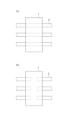
- FIGS. 1(a) and 1(b) schematically show an electrode structure in which the silver finger electrodes 2 arranged on the light receiving surface side are covered with the first copper bus electrodes 1.
- FIG. The silver finger electrodes 2 may be formed continuously from one end of the substrate to the other, as shown in FIG. You may form discontinuously in the part covered with 1.
- FIG. 1(a) and 1(b) schematically show an electrode structure in which the silver finger electrodes 2 arranged on the light receiving surface side are covered with the first copper bus electrodes 1.
- FIG. The silver finger electrodes 2 may be formed continuously from one end of the substrate to the other, as shown in FIG. You may form discontinuously in the part covered with 1.
- the solar cell according to this embodiment can be produced, for example, by the following method.
- a silicon wafer having a texture structure on the surface and forming a p/n junction can be used.
- a layer of Al 2 O 3 is deposited on the back side by atomic layer deposition (ALD), and a plasma-assisted chemical vapor deposition is performed on the Al 2 O 3 layer.
- a SiN layer is formed by a growth method (PECVD).
- PECVD a partial opening is formed in the arranged SiN layer/Al 2 O 3 layer by laser light.
- an aluminum paste for forming aluminum bus electrodes and aluminum finger electrodes is printed by a screen printer.
- the SiN layer has an antireflection role.
- the Al 2 O 3 layer has a role of passivation. Since both the SiN layer and the Al 2 O 3 layer have insulating properties, they also function as insulating layers on the substrate.
- a SiN layer is formed on the light-receiving surface, and then silver paste for forming finger electrodes is printed.
- the silicon substrate on which each of the above pastes is printed is subjected to heat treatment (fire-through) in which the silicon substrate is heated in the atmosphere at a temperature of 600° C. to 900° C. for several minutes.
- heat treatment fire-through
- connection between the silver finger electrodes and the silicon substrate is obtained on the light-receiving surface of the silicon substrate, and connection between the aluminum bus electrodes and the aluminum finger electrodes and the silicon substrate is obtained on the back surface.
- a copper paste for forming the second copper bus electrodes is partially printed on the aluminum bus electrodes on the back side.
- a copper paste for forming the first copper bus electrodes is printed so as to cover the silver finger electrodes.
- the substrate on which these copper pastes are printed is dried in the air at 100° C. for 3 minutes, and then subjected to an oxidizing heat treatment by heating in the air, so that the copper paste is changed to copper oxide and sintered.
- the substrate obtained above is subjected to a reduction heat treatment in which it is heated in a reducing gas atmosphere, and the copper oxide is changed to copper to obtain the first copper bus electrode and the second copper bus electrode.
- the heating conditions for the oxidation heat treatment or reduction heat treatment 300 to 420° C. and 1 to 30 minutes can be used.
- a mixed gas containing hydrogen (eg, 3% by volume) and nitrogen can be used as the reducing gas atmosphere.
- the aluminum bus electrode arranged on the back surface side of the substrate in the solar cell according to this embodiment is formed of a sintered body of fine particles containing aluminum, and a second copper bus electrode is formed on part of the aluminum bus electrode. is formed.
- the sintered body of the aluminum bus electrode has a region having an alloy containing aluminum and copper near the end of the interface between the aluminum bus electrode and the second copper bus electrode. Near the edge of the interface between the aluminum bus electrode and the second copper bus electrode, the aluminum of the aluminum bus electrode and the copper of the second copper bus electrode react to form an alloy containing aluminum and copper in the sintered body. A region is formed. The alloy region can enhance the adhesion between the copper bus electrode and the contact electrode.
- FIGS. 2(a) to 2(c) are scanning electron microscope (SEM) images of a region including the aluminum bus electrode 4 arranged on the back side and the second copper bus electrode 3 partially overlapping thereon. ) is an SEM image observed in .
- the respective portions of the second copper bus electrodes 3 and aluminum bus electrodes 4 formed using copper paste and aluminum paste can be distinguished based on the size and shape of the particles, as shown in FIG. 2(a). Therefore, the structure near the interface between the aluminum bus electrode 4 and the second copper bus electrode 3 can be specified.
- FIG. 3 is a diagram schematically showing the cross-sectional structure along the line A-A' marked in FIG. 2(a).
- the second copper bus electrodes 3 are arranged to partially cover the aluminum bus electrodes 4, so that the second copper bus electrodes 3 and the aluminum bus electrodes 4 overlap each other.
- a portion 8 is formed.
- the aluminum bus electrode 4 is in contact with the Al finger electrodes 10 on the side opposite to the overlapping portion 8 .
- the interface 7 where the second copper bus electrode 3 and the aluminum bus electrode 4 are in contact continues to the end of the overlapping portion 8 .
- the edge of the interface located at the edge of the overlapping portion 8 is at the position indicated by reference numeral 9 in FIG. This specification refers to the edge of the above interface as the "interface edge”.
- the interface edge 9 can be identified at the position indicated by the white dotted line in the SEM image of FIG. 2(a).
- FIG. 2(b) shows region X remote from the interface edge and FIG. 2(c) shows region Y adjacent to the interface edge.
- the image contrast of region Y shows patchy tissue compared to the image contrast of region X.
- SEM-EDX X-ray energy dispersive spectroscopy
- the region of the sintered body at a distance of 5 ⁇ m or more and 170 ⁇ m or less from the end of the interface between the aluminum bus electrode and the second copper bus electrode contains an alloy containing aluminum and copper. ing.
- a region having an alloy containing aluminum and copper may be hereinafter referred to as an "alloy layer.” The above specified distances for the alloy layers are explained below.
- the range of the area where the alloy layer is formed can be determined, for example, as follows. Observe the surface texture of the Al bus electrode at a magnification of 4000 times using SEM. At this time, the observation area is moved from the interface edge toward the Al finger electrode, and a plurality of SEM images are taken. In these SEM images, as shown in FIGS. 2(b) and 2(c), alloy particles exhibiting a mottled structure and Al particles not exhibiting a mottled structure can be clearly distinguished. It connects multiple images and draws multiple rectangular frames in them. The first rectangle is arranged so that one long side overlaps with the interface end portion 9 and the other long side is included in the Al bus electrode side.
- the structure within the rectangular frame is observed, and the number of alloy particles and Al particles contained within the frame is determined.
- the first rectangular region is determined to be an alloy layer.
- the alloy layer containing aluminum and copper in this embodiment is specified by such a method.
- the distance from the edge of the interface is determined to be zero.
- the second rectangle is arranged at a position farther from the interface edge than the first rectangle, and one of the long sides of the second rectangle is the Al bus electrode of the first rectangle. Place it so that it overlaps with the long side on the side. Then, the texture within the frame was observed in the same manner as for the first rectangle, and the ratio of the number of particles exhibiting a patchy texture was measured. If the particles exhibit a patchy texture, the second rectangular area is determined to be the alloy layer.
- the second rectangle is not an alloy layer
- it is determined that the distance from the edge of the interface is 5 ⁇ m. do.
- the alloy layer containing the alloy containing aluminum and copper is preferably present in a range at a distance of 5 ⁇ m or more and 170 ⁇ m or less from the end of the interface between the aluminum bus electrode and the copper bus electrode. If the alloy layer expands beyond 170 ⁇ m, copper may diffuse into the silicon substrate in contact with the aluminum bus electrode, greatly deteriorating battery characteristics.
- the lower limit of the distance from the edge of the interface to the edge of the alloy layer is preferably 5 ⁇ m or more, more preferably 10 ⁇ m or more, and even more preferably 15 ⁇ m or more and 47 ⁇ m or more.
- the upper limit of the distance is preferably 170 ⁇ m or less, more preferably 100 ⁇ m or less, and particularly preferably 91 ⁇ m or less. Even if the heat treatment temperature and heat treatment time are changed, the conditions may be selected so that the distance from the interface edge to the alloy layer edge is in the range of 5 ⁇ m or more and 170 ⁇ m or less.
- At least one of the first copper bus electrode and the second copper bus electrode of the solar cell according to the present embodiment contains copper and has a softening point of 450° C. or less Te oxide (tellurium oxide) or Se It preferably contains at least one kind of oxide (selenium oxide).
- the first copper bus electrode and the second copper bus electrode may be collectively referred to as "copper bus electrode”.
- the copper bus electrodes are made by firing the copper paste printed on the insulating layer. If an oxide that softens or melts at the firing temperature is contained in the copper paste, the oxide softens or melts and then cools and distributes due to the firing process. As a result, the adhesion between the oxide and the insulating layer is enhanced, and the bus electrode can be prevented from peeling off from the insulating layer. From that point of view, the copper bus electrode preferably contains at least one of Te oxide and Se oxide having a softening point of 450° C. or lower.
- the copper paste containing an oxide having a softening point of 450° C. or lower can be fired at a low temperature, Cu diffuses into the silicon substrate through the silver finger electrodes or the Al bus electrodes during the firing process. can prevent you from doing it.
- Mixing Te oxide and Se oxide is preferable because the melting point can be lowered to 350° C. or lower.
- oxides of tellurium (Te) and selenium (Se) there are oxides of bismuth (Bi), vanadium (V), and the like.
- the softening point of the oxide according to this embodiment is defined as the temperature at the fourth inflection point obtained by differential thermal analysis.
- the distribution of Te oxide or Se oxide contained in the copper bus electrode corresponds to the distribution of Te or Se.
- This embodiment specified the copper bus electrode based on the percentage of the area where Te or Se is distributed. That is, in the cross section perpendicular to the length direction of the copper bus electrode, the ratio of the area where Te (tellurium) or Se (selenium), which is a constituent element of Te oxide or Se oxide, is distributed is 4% or more and 45%. The following are preferable. In this specification, the above-mentioned "ratio of area” is hereinafter referred to as "area ratio". If the area ratio of Te or Se is less than 4%, the adhesion may be insufficient.
- the lower limit of the area ratio of Te or Se is preferably 4% or more, more preferably 10% or more, and still more preferably 13% or more.
- the upper limit of the area ratio is preferably 45% or less, more preferably 40% or less.
- a sample obtained by a predetermined manufacturing method has Cu bus electrodes and Ag finger electrodes formed on the light receiving surface side. After exposing a cross section of the sample perpendicular to the longitudinal direction of the Cu bus electrode, the composition distribution of the cross section was examined using a scanning electron microscope (SEM) and an X-ray energy dispersive spectrometer (SEM-EDX). Ta. Samples subjected to cross-sectional observation were produced from arbitrary five points on the Cu bus electrode.
- FIG. 4(a) shows an SEM image of the cross-sectional structure.
- FIGS. 1 shows an SEM image of the cross-sectional structure.
- FIG. 4(b), (c), and (d) respectively show composition distribution images of Cu, Ag, and Te elements obtained by SEM-EDX, and Cu is present in FIG. 4(b). Regions and regions where Te exists in FIG. 4(d) are shown in white.
- the area of Te distribution and the area of Cu distribution were measured at five arbitrarily selected points in the cross section, and the area ratio of Te was obtained by dividing the area of Te by the total area of Cu and Te. Their average value was taken as the area ratio of Te.
- the area ratio of Te was calculated to be 6.4%. Since the distribution of Te corresponds to the distribution of Te oxide, the effect of Te oxide can be evaluated based on the area ratio of Te. The same applies to the area ratio of Se.
- thermoplastic organic polymer In order to ensure adhesion between the copper bus electrode and the insulating layer, an organic layer may be provided near the interface between the copper bus electrode and the insulating layer.
- the copper bus electrode of the solar cell according to this embodiment preferably contains a thermoplastic organic polymer having a glass transition temperature of 300° C. or higher and 450° C. or lower.
- the ratio of the area where carbon, which is a constituent element of the thermoplastic organic polymer, is distributed is preferably 9% or more and 40% or less.
- the bus electrode containing a thermoplastic organic polymer having a glass transition temperature of 300°C or higher and 450°C or lower, which constitutes the organic layer, can enhance adhesion with the insulating layer.
- the bus electrodes are produced by the firing process, they are not thermally decomposed, but are softened or melted, and then cooled to form bus electrodes in close contact with the insulating layer.
- the glass transition temperature of the thermoplastic organic polymer is lower than 300° C., the viscosity of the organic material layer decreases during firing of the bus electrodes, and the amount of the organic material layer that penetrates into the voids of the bus electrodes increases. Since the amount of the organic layer present at the interface between the two is reduced, the adhesion strength may be reduced.
- the glass transition temperature is higher than 450°C, there is a possibility that sufficient adhesion strength cannot be obtained.
- the size of the organic layer formed near the interface can be evaluated by the ratio of the area where the carbon contained in the thermoplastic organic polymer forming the organic layer is distributed.
- the "area ratio” is hereinafter referred to as "area ratio”.
- the area ratio of carbon can be obtained by SEM-EDX analysis of the cross section of the bus electrode in the same manner as the measurement method described for the area ratio of Te.
- the area ratio of carbon in the cross section perpendicular to the length direction of the bus electrode is preferably 9% or more and 40% or less. If the area ratio of carbon is less than 9%, the adhesion strength between the bus electrode and the insulating layer is reduced.
- the area ratio of carbon exceeds 40%, a problem may occur that the solder does not sufficiently adhere to the bus electrodes in the process of soldering the TAB wires to the bus electrodes.
- the lower limit of the carbon area ratio is preferably 9% or more, more preferably 25% or more.
- the upper limit of the carbon area ratio is preferably 40% or less.
- the glass transition temperature of the thermoplastic organic polymer constituting the organic layer is defined as the temperature at which the loss tangent measured by dynamic viscoelasticity measurement becomes maximum.
- the solar cell according to this embodiment has a laminated structure in which part or all of the finger electrodes are composed of first-layer electrodes and second-layer electrodes.
- the electrode of the first layer contains silver, penetrates through the insulating layer and is in contact with the surface of the silicon substrate.
- a second layer electrode comprises copper and is disposed on the first layer.
- the line width of the first layer electrode is 15 ⁇ m or more and 60 ⁇ m or less, the line width of the second layer electrode is 20 ⁇ m or more and 100 ⁇ m or less, and is wider than the line width of the first layer electrode, It is preferable that the end in the width direction is in contact with the insulating layer.
- the line widths of the electrodes of the first layer and the line width of the second layer are too small, a sufficient amount of the paste will not be extruded from the openings of the screen printing plate during paste printing, making it impossible to form continuous wiring.
- the line width is too large, the light-receiving area is reduced, resulting in degradation of conversion efficiency.
- the line width of the electrodes of the second layer must be wider than that of the electrodes of the first layer in order to conduct electricity from the electrodes of the first layer to the outside.
- the second layer electrode contains copper, it is preferable that the portion other than the portion in contact with the first layer electrode is in contact with the insulating layer in order to suppress the diffusion of Cu into the substrate.
- the electrodes of the first layer contain silver, penetrate through the insulating layer and are in contact with the surface of the silicon substrate, and are spaced apart in the length direction.
- the length of each electrode of the first layer is 1 mm or more and 10 mm or less, and the distance between the electrodes of the first layer is 1 mm or more and 5 mm or less in the length direction and 0.8 mm in the width direction. 2 mm or less.
- the electrodes of the second layer contain copper, are arranged in contact with the electrodes of the first layer, and electrically connect the spaced electrodes of the first layer.
- the arrangement form of the silver finger electrodes of the first layer may be continuous from one end of the substrate to the other end, or may be divided in the middle.
- the length of each electrode of the first layer and the distance between the electrodes of the first layer within the above-specified range, carriers inside the silicon substrate can be efficiently discharged from the emitter. It is preferable in terms of shifting to the electrodes of the first layer.
- the copper finger electrodes of the second layer are preferable in that the carriers in the substrate can be extracted to the outside by connecting the individual silver finger electrodes.
- the length and width of the electrodes of the first layer are larger than the above-specified ranges, the light-receiving area becomes small, resulting in degradation of conversion efficiency.
- the length and width of the electrodes of the first layer are smaller than the ranges specified above, the rate at which the photoinduced carriers generated in the substrate recombine and disappear before reaching the electrodes of the first layer is increased, and the fill factor (FF) and open-circuit voltage (Voc) are decreased.
- Example 1 Distance from Interface Edge to Alloy Layer
- a silicon substrate having a textured structure on the surface and having a p/n junction was used.
- An Al 2 O 3 layer was formed on the back surface of the silicon substrate by atomic layer deposition (ALD), and a SiN layer was formed on the Al 2 O 3 layer by plasma enhanced chemical vapor deposition (PECVD).
- PECVD plasma enhanced chemical vapor deposition
- a laser beam was then used to form a partial opening in the SiN layer/Al 2 O 3 layer.
- an aluminum paste for forming Al bus electrodes and Al finger electrodes was printed by screen printing.
- a SiN layer was formed on the light-receiving surface of the silicon substrate, and silver paste was printed thereon.
- the silicon substrate was subjected to heat treatment at 600° C. for 3 minutes in the atmosphere (this heat treatment is also called “fire-through”) to form silver finger electrodes and Al bus electrodes.
- a copper paste was partially printed on the Al bus electrode on the back surface of the obtained substrate.
- a copper paste for forming the first copper bus electrodes was printed on the light receiving surface side of the substrate so as to cover the silver finger electrodes.
- the substrate after printing was dried in the atmosphere at 100° C. for 3 minutes, and then subjected to oxidation heat treatment in the atmosphere at a predetermined temperature for 3 minutes to change the copper paste into copper oxide.
- the obtained substrate was subjected to reduction heat treatment for 3 minutes at a predetermined temperature in a mixed gas atmosphere of 3% by volume of hydrogen and the balance of nitrogen to form the first copper bus electrodes from copper oxide.
- a sample was made. The same heating temperature was applied to the above oxidation heat treatment and reduction heat treatment.
- the rate of change of Rs ( ⁇ Rs) and the rate of change of Rsh ( ⁇ Rsh) were calculated by the following formulas (1) and (2). Table 1 shows the results.
- Judgments A to D shown in the overall judgment in Table 1 are classified according to the following criteria.
- Judgment A The absolute values of both ⁇ Rs and ⁇ Rsh are less than 0.2.
- Judgment B The absolute values of both ⁇ Rs and ⁇ Rsh are less than 0.3.
- Judgment C The absolute values of both ⁇ Rs and ⁇ Rsh are less than 1.0.
- Determination D The absolute value of either ⁇ Rs or ⁇ Rsh is 1.0 or more. Judgments A, B, and C were evaluated as good, and judgment D was evaluated as unsuitable.
- Example 2 Area ratio of Te Te oxide particles were added to the paste containing the copper particles at the weight ratio (%) shown in Table 2.
- the weight ratio is the ratio (%) of the weight of the oxide particles to the total value of the weight of the copper particles and the weight of the oxide particles.
- a TAB wire with a width of 1.4 mm was soldered to each sample, and the solderability was evaluated by lifting the soldered TAB wire by hand.
- the TAB wire was lifted by hand the case where the TAB wire adhered to the sample was judged as "acceptable”, and the case where the TAB wire was separated from the sample was judged as "impossible”.
- the TAB wire was pulled perpendicularly to the sample surface, and the tensile strength (N) of the TAB wire when the TAB wire was peeled off from the sample was measured. Table 2 shows the measurement results thereof.
- Example 3 Area ratio of carbon contained in thermoplastic organic polymer
- a polyimide powder having a glass transition temperature of 190 ° C. and a melting point of 320 ° C. is added to the weight ratio (%) shown in Table 3. was added with The weight ratio is the ratio (%) of the weight of the polyimide powder to the sum of the weight of the copper particles and the weight of the powder.
- a sample having a copper bus electrode was produced by selecting an oxidation heat treatment temperature and a reduction heat treatment temperature of 380° C. in the same procedure as in Example 1.
- Test Examples 3-2 to 3-4 in which the area ratio of carbon is within the range of the present invention (9% or more and 40% or less), were evaluated as A, and the solderability was good. As a result, a solar cell having a TAB wire with high tensile strength was obtained. On the other hand, Test Examples 3-1, 3-5, and 3-6, which are outside the scope of the present invention, were judged as D, and the solderability and adhesive strength of the TAB wire were unsuitable.
- Example 4 Line width of the first layer and line width of the second layer
- a predetermined electrode was produced on the back side of the substrate.
- a silver paste was printed in the same procedure as in Example 1, followed by a drying process and a fire-through heat treatment to form finger electrodes with a thickness of 5 to 8 ⁇ m (hereinafter referred to as “ (referred to as "first layer electrode”) was formed.
- a copper paste is printed so as to overlap the electrodes of the first layer, dried in the air at 100 ° C. for 3 minutes, and then subjected to oxidation heat treatment at 380 ° C. in the atmosphere for 3 minutes, and then in a reducing atmosphere.
- a reduction heat treatment was performed at 380° C. for 3 minutes in (a mixed gas atmosphere containing 3% by volume of hydrogen gas in argon gas) to form a second layer electrode containing copper.
- the electrodes of the second layer were formed so that the ends in the width direction were in contact with the insulating layer.
- the total thickness of the electrodes of the first layer and the thickness of the electrodes of the second layer was 20 to 40 ⁇ m.
- Various samples were prepared having line widths shown in Table 4 for the first layer electrode and the second layer electrode.
- the open circuit voltage (Voc) (unit: V) and series resistance (Rs) (unit: m ⁇ ) were measured. Furthermore, in order to evaluate the adhesion between the electrodes and the substrate, a tape test was performed to check whether the electrodes were separated from the substrate. In the comprehensive judgment, the criteria for judgment A are Voc of 0.74 or more, Rs of 500 or less, and peeling in the tape test of "no (adhesion)". Criteria for judgment B are Voc of less than 0.74, Rs of 650 or less, and no delamination in the tape test. The criterion for judgment D is "yes" in the tape test.
- a solar cell with a judgment of A or B is evaluated as having good conversion characteristics and adhesiveness, and a solar cell with a judgment of C is evaluated as unsuitable.
- the line width of the first layer electrode and the line width of the second layer electrode are within the range of the present invention (the line width of the first layer electrode is 15 ⁇ m or more and 60 ⁇ m or less, the second layer electrode Test Examples 4-2 to 4-6 included in the line width of 20 ⁇ m or more and 100 ⁇ m or less) were judged A and B, and showed good conversion characteristics and adhesion.
- Test Example 4-1 which is outside the scope of the present invention, was judged C, and was unsuitable for conversion characteristics and adhesiveness.
- Example 5 Line width of the first layer
- Example 5 Line width of the first layer
- Example 6 First layer electrode length, lengthwise spacing, and widthwise spacing A condition was selected in which the line width of the second layer electrode was 50 ⁇ m. Then, when forming the electrodes of the first layer, the silver paste is printed so as to be arranged at regular intervals in the length direction, and the drying treatment and the fire-through treatment are performed by the same procedure as in Example 4. to prepare a first layer silver finger electrode. Copper paste was then printed to form a continuous second layer electrode overlying the top of the first layer and connecting the spaced first layer electrodes. After that, according to the same procedure as in Example 4, air drying was performed at 100 ° C. for 3 minutes, and then oxidation heat treatment and reduction heat treatment were performed at 380 ° C. for 3 minutes to obtain a sample having a second layer electrode. made.
- Test Example 6 included in the scope of the present invention (the electrode length of the first layer is 1 mm or more and 15 mm or less, the distance in the length direction is 1 mm or more and 7 mm or less, the distance in the width direction is 0.8 mm or more and 2 mm or less) -2 to 6-5 were rated A and exhibited good conversion properties and adhesion.
- Test Example 6-1 which is outside the scope of the present invention, was judged C, and was unsuitable for conversion characteristics and adhesiveness.
Abstract
The present invention provides a solar cell which employs copper as an electrode material, while having good solar cell characteristics and adhesion. A solar cell according to the present invention has a configuration in which: a silver finger electrode 2 and a first copper bus electrode 1 are arranged on the light-receiving surface side of a silicon substrate; the first copper bus electrode 1 covers a part of the silver finger electrode 2; an Al finger electrode, an Al bus electrode 4 and a second copper bus electrode 3 are arranged on the back surface side of the silicon substrate; the Al finger electrode and the Al bus electrode 4 are formed of a sintered body of fine particles that contain aluminum; the second copper bus electrode 3 covers a part of the Al bus electrode 4; and the Al bus electrode 4 contains an alloy, which contains aluminum and copper, in a region of the sintered body extending from a position that is 5 µm away from an interfacial edge 9 between the Al bus electrode 4 and the second copper bus electrode 3 to a position that is 170 µm away from the interfacial edge 9.
Description
本発明は、太陽電池の電極配線及びその周辺構造に関するものである。
The present invention relates to electrode wiring of a solar cell and its peripheral structure.
再生可能エネルギー源として太陽電池の必要性が高まっている。従来、集電電極であるバス電極およびフィンガー電極の材料として、高価な銀を有する銀ペーストが用いられているため、当該電極の低コスト化が困難である。そのため、銀(Ag)電極を銅(Cu)電極へ転換してコスト低減をする提案が行われている。以下、銀を「Ag」、銅を「Cu」、シリコンを「Si」と記載することもある。
The need for solar cells as a renewable energy source is increasing. Conventionally, silver paste containing expensive silver has been used as a material for bus electrodes and finger electrodes, which are current collecting electrodes, making it difficult to reduce the cost of the electrodes. Therefore, a proposal has been made to convert the silver (Ag) electrode to a copper (Cu) electrode to reduce the cost. Hereinafter, silver may be referred to as "Ag", copper as "Cu", and silicon as "Si".
その一例として、特許文献1は、シリコン半導体基板1と、Cu含有金属層4と、Ag含有フィンガー配線4と、酸化物または有機化合物を含む界面層3と、を有する太陽電池装置10において、前記Ag含有フィンガー配線4が前記シリコン半導体基板1の受光面側に積層され、前記界面層3が前記シリコン半導体基板1の受光面側に積層され、前記Cu含有金属層4が前記界面層3の上に積層され、かつ、前記Ag含有フィンガー配線2と離間して配置された、太陽電池装置10を提案している。しかし、Cu含有金属層とAg含有フィンガー配線との間には絶縁性の界面層が存在するため、配線全体の電気抵抗が高くなる。その結果、太陽電池セルの直列抵抗が高くなるため、曲線因子(FF)および変換効率が劣化する。
As an example, Patent Document 1 discloses a solar cell device 10 having a silicon semiconductor substrate 1, a Cu-containing metal layer 4, an Ag-containing finger wiring 4, and an interface layer 3 containing an oxide or an organic compound. The Ag-containing finger wiring 4 is laminated on the light receiving surface side of the silicon semiconductor substrate 1, the interface layer 3 is laminated on the light receiving surface side of the silicon semiconductor substrate 1, and the Cu-containing metal layer 4 is laminated on the interface layer 3. , and spaced apart from the Ag-containing finger wires 2 are proposed. However, since there is an insulating interfacial layer between the Cu-containing metal layer and the Ag-containing finger wiring, the electrical resistance of the wiring as a whole increases. As a result, the series resistance of the photovoltaic cell increases, deteriorating the fill factor (FF) and conversion efficiency.
また、銅電極とシリコン基板との間の導電性を高めるため、銅電極がシリコン基板に直接的に接するように配置された場合、銅電極のCuとシリコン基板のSiとが相互拡散を起こすことに加えて、Si中のCu拡散速度が非常に速いという問題がある(非特許文献1参照)。シリコン基板中に進入したCuは、シリコンバンドギャップの深いエネルギー位置にアクセプター準位を形成し、ダイオード内のキャリア寿命を短縮させるため、開放電圧(Voc)が減少し、太陽電池特性を劣化させる原因となる。
Further, in order to increase the conductivity between the copper electrode and the silicon substrate, when the copper electrode is arranged so as to be in direct contact with the silicon substrate, interdiffusion between Cu in the copper electrode and Si in the silicon substrate occurs. In addition to this, there is a problem that the diffusion rate of Cu in Si is very high (see Non-Patent Document 1). Cu that has entered the silicon substrate forms an acceptor level at a deep energy position in the silicon bandgap and shortens the carrier life in the diode. becomes.
上述したように、太陽電池装置の製造コストを低減するため、バス電極及びフィンガー電極の材料として、高価な銀を安価な銅へ転換する場合、電極材料の銅は、シリコン基板中へ容易に拡散して太陽電池特性の劣化を招くという課題がある。さらに、この銅の拡散を防止するために、銅電極とシリコン基板との間に界面層を配置する場合、配線全体の電気抵抗が高くなり、セルの直列抵抗(Rs)が増加するので、曲線因子(FF)及び変換効率が劣化するという課題がある。また、銅電極は、シリコン基板および反射防止膜(SiN、SiO2など)などの銅電極の下部に配置される材料との密着性が不十分であるため、銅電極がセル表面から剥離するという課題もある。
As described above, in order to reduce the manufacturing cost of the solar cell device, when expensive silver is replaced with inexpensive copper as the material of the bus electrodes and finger electrodes, the electrode material copper easily diffuses into the silicon substrate. As a result, there is a problem that deterioration of solar cell characteristics is caused. Furthermore, if an interfacial layer is placed between the copper electrode and the silicon substrate to prevent this copper diffusion, the electrical resistance of the entire wiring will be higher, increasing the series resistance (Rs) of the cell, so the curve There is a problem that the factor (FF) and conversion efficiency deteriorate. In addition, the copper electrode is said to peel off from the cell surface because the adhesion of the copper electrode to the silicon substrate and the materials placed under the copper electrode such as anti-reflection coatings (SiN, SiO2, etc.) is insufficient. There are also challenges.
本発明は、太陽電池において銀電極を銅電極へ転換しても、良好な太陽電池特性及び密着性を有する太陽電池を提供することを目的とする。
An object of the present invention is to provide a solar cell that has good solar cell characteristics and adhesion even if the silver electrode in the solar cell is replaced with a copper electrode.
本発明者らは、上記の課題について検討し、Cu含有バス電極の組成を調整することにより、TAB線のはんだ付け特性を犠牲にすることなく、Cu電極とその下地との密着性を高めることができることを見出した。さらに、Cu含有バス電極のCuがAg電極及びAl電極を介してシリコン基板の中へ拡散することを抑止できることを見出し、本発明を完成するに至った。具体的には、本発明は、以下の(1)~(5)の実施態様を含む。
The inventors of the present invention have studied the above problems and have found that by adjusting the composition of the Cu-containing bus electrode, the adhesion between the Cu electrode and its underlying layer can be improved without sacrificing the solderability of the TAB wire. I found out what I can do. Furthermore, the inventors have found that Cu in the Cu-containing bus electrode can be prevented from diffusing into the silicon substrate through the Ag electrode and the Al electrode, and have completed the present invention. Specifically, the present invention includes the following embodiments (1) to (5).
(1)本発明に係る実施態様は、シリコン基板を有する太陽電池において、
前記シリコン基板は、その表面の一部に絶縁層を有しており、
前記シリコン基板の受光面側には、銀フィンガー電極及び第1の銅バス電極が配置され、
前記銀フィンガー電極は、銀を含み、前記シリコン基板の表面に接しており、
前記第1の銅バス電極は、少なくとも銅を含み、前記銀フィンガー電極の一部の上を覆っており、前記銀フィンガー電極以外の部分では前記絶縁層に接しており、
前記シリコン基板の裏面側には、アルミニウムフィンガー電極、アルミニウムバス電極及び第2の銅バス電極が配置され、
前記アルミニウムフィンガー電極及び前記アルミニウムバス電極は、アルミニウムを含む微粒子の焼結体により形成され、
前記アルミニウムバス電極においては、その一部が前記第2の銅バス電極によって覆われており、前記アルミニウムバス電極と前記第2の銅バス電極との界面端部から5μm以上、170μm以下の距離にある前記焼結体の領域が、アルミニウム及び銅を含む合金を有している、太陽電池である。 (1) An embodiment according to the present invention is a solar cell having a silicon substrate,
The silicon substrate has an insulating layer on a part of its surface,
A silver finger electrode and a first copper bus electrode are arranged on the light receiving surface side of the silicon substrate,
the silver finger electrodes contain silver and are in contact with the surface of the silicon substrate;
The first copper bus electrode contains at least copper, covers a part of the silver finger electrode, and is in contact with the insulating layer in a part other than the silver finger electrode,
Aluminum finger electrodes, aluminum bus electrodes and second copper bus electrodes are arranged on the back side of the silicon substrate,
The aluminum finger electrodes and the aluminum bus electrodes are formed of a sintered body of fine particles containing aluminum,
A part of the aluminum bus electrode is covered with the second copper bus electrode, and a distance of 5 μm or more and 170 μm or less from the interface end between the aluminum bus electrode and the second copper bus electrode is provided. A solar cell wherein a region of the sintered body comprises an alloy containing aluminum and copper.
(2)本発明に係る実施態様は、前記第1の銅バス電極または前記第2の銅バス電極は、軟化点が450℃以下である、Te酸化物またはSe酸化物の少なくとも一種を含み、
前記銅バス電極の長さ方向に垂直な断面において、前記Te酸化物または前記Se酸化物の構成元素であるTeまたはSeが分布する面積の割合が、4%以上、45%以下である、上記(1)に記載の太陽電池である。 (2) In an embodiment according to the present invention, the first copper bus electrode or the second copper bus electrode contains at least one Te oxide or Se oxide having a softening point of 450° C. or less,
In the cross section perpendicular to the length direction of the copper bus electrode, the percentage of the area where Te or Se, which is a constituent element of the Te oxide or the Se oxide, is 4% or more and 45% or less. (1) is a solar cell.
(3)本発明に係る実施態様は、前記第1の銅バス電極または前記第2の銅バス電極は、ガラス転移温度が300℃以上、450℃以下である熱可塑性有機高分子を含み、
前記銅バス電極の長さ方向に垂直な断面において、前記熱可塑性有機高分子の構成元素である炭素が分布する面積の割合が、9%以上、40%以下である、上記(1)または(2)に記載の太陽電池である。 (3) In an embodiment according to the present invention, the first copper bus electrode or the second copper bus electrode contains a thermoplastic organic polymer having a glass transition temperature of 300° C. or more and 450° C. or less,
(1) or ( 2) is the solar cell described in .
(4)本発明に係る実施態様は、前記銀フィンガー電極の一部または全部が第一層の電極と第二層の電極とからなる積層構造を有しており、
前記第一層の電極は、銀を含み、前記絶縁層を貫通して前記シリコン基板の表面に接しており、
前記第二層の電極は、銅を含み、前記第一層の電極の上に配置されており、
前記第一層の電極の線幅は、15μm以上、60μm以下であり、
前記第二層の電極の線幅は、20μm以上、100μm以下であり、前記第一層の電極の線幅より広く、幅方向の端部は前記絶縁層と接している、上記(1)または(2)に記載の太陽電池である。 (4) In an embodiment according to the present invention, part or all of the silver finger electrode has a laminated structure consisting of a first layer electrode and a second layer electrode,
the electrode of the first layer contains silver, penetrates the insulating layer and is in contact with the surface of the silicon substrate;
the second layer electrode comprises copper and is disposed on the first layer electrode;
The line width of the electrode of the first layer is 15 μm or more and 60 μm or less,
The line width of the electrode of the second layer is 20 μm or more and 100 μm or less, is wider than the line width of the electrode of the first layer, and the end in the width direction is in contact with the insulating layer, or (2) is the solar cell.
(5)本発明に係る実施態様は、前記銀フィンガー電極の一部が第一層の電極と第二層の電極とからなる積層構造を有しており、
前記第一層の電極は、銀を含み、前記絶縁層を貫通して前記シリコン基板の表面に接しており、長さ方向に間隔を空けて配置され、前記第一層の個々の電極の長さは、1mm以上、15mm以下であり、前記第一層の電極同士の間隔は、長さ方向が1mm以上、7mm以下であり、幅方向が0.8mm以上、3mm以下であり、
前記第二層の電極は、銅を含み、前記第一層の電極に接して配置されており、離間した前記第一層の電極同士を電気的に接続する、上記(1)または(2)に記載の太陽電池である。 (5) In an embodiment according to the present invention, part of the silver finger electrode has a laminated structure consisting of a first layer electrode and a second layer electrode,
The electrodes of the first layer comprise silver, extend through the insulating layer and contact the surface of the silicon substrate, are spaced longitudinally, and are spaced apart lengthwise of the individual electrodes of the first layer. the distance between the electrodes of the first layer is 1 mm or more and 7 mm or less in the length direction and 0.8 mm or more and 3 mm or less in the width direction;
(1) or (2) above, wherein the electrodes of the second layer contain copper, are arranged in contact with the electrodes of the first layer, and electrically connect the electrodes of the first layer that are spaced apart; The solar cell described in .
本発明によれば、太陽電池のバス電極として安価な銅バス電極を適用できるとともに、Cuバス電極とその下地との密着性が良好である太陽電池を提供することができる。さらに、電極を形成するための焼成温度の低温化が可能となり、銅バス電極のCuがAgフィンガー電極およびAlフィンガー電極を介してシリコン基板の中へ拡散することを抑止できる。本発明によれば、性能と信頼性を損ねることなく、太陽電池の製造コストを大幅に低減することができる。
According to the present invention, an inexpensive copper bus electrode can be applied as the bus electrode of the solar cell, and a solar cell in which the adhesion between the Cu bus electrode and its underlying layer is good can be provided. Furthermore, the baking temperature for forming the electrodes can be lowered, and the Cu of the copper bus electrodes can be prevented from diffusing into the silicon substrate through the Ag finger electrodes and the Al finger electrodes. ADVANTAGE OF THE INVENTION According to this invention, the manufacturing cost of a solar cell can be reduced significantly, without impairing performance and reliability.
以下、本発明の実施の形態について説明する。本発明は、この実施の形態により限定されるものではない。なお、本明細書において、「X~Y」(X、Yは任意の数値)との表記は、「X以上Y以下」を
意味する。 BEST MODE FOR CARRYING OUT THE INVENTION Embodiments of the present invention will be described below. The present invention is not limited by this embodiment. In this specification, the notation "X to Y" (X and Y are arbitrary numerical values) means "X or more and Y or less".
意味する。 BEST MODE FOR CARRYING OUT THE INVENTION Embodiments of the present invention will be described below. The present invention is not limited by this embodiment. In this specification, the notation "X to Y" (X and Y are arbitrary numerical values) means "X or more and Y or less".
(太陽電池の基本構造)
本実施形態に係る太陽電池は、シリコン基板を有しており、当該シリコン基板は、その表面の一部に絶縁層を有している。シリコン基板の受光面側には、銀フィンガー電極及び第1の銅バス電極が配置され、シリコン基板の裏面側には、アルミニウムフィンガー電極、アルミニウムバス電極及び第2の銅バス電極が配置されている。上記絶縁層は、SiN、SiO2、Al2O3などの材料により形成することができる。シリコン基板の表面のうち、上記「受光面」は、太陽光が当たる側の表面を指しており、上記「裏面」は、受光面と反対側に位置する表面を指している。本明細書では、上記「シリコン基板」を単に「基板」と記載することもある。 (Basic structure of solar cell)
The solar cell according to this embodiment has a silicon substrate, and the silicon substrate has an insulating layer on a part of its surface. Silver finger electrodes and first copper bus electrodes are arranged on the light receiving surface side of the silicon substrate, and aluminum finger electrodes, aluminum bus electrodes and second copper bus electrodes are arranged on the back surface side of the silicon substrate. . The insulating layer can be formed of a material such as SiN, SiO2 , Al2O3 . Of the surfaces of the silicon substrate, the "light-receiving surface" refers to the surface that is exposed to sunlight, and the "rear surface" refers to the surface opposite to the light-receiving surface. In this specification, the "silicon substrate" may be simply referred to as "substrate".
(電極の構造)
前記銀フィンガー電極は、銀を含み、前記シリコン基板の表面に接している。前記第1の銅バス電極は、少なくとも銅を含んでいる。前記アルミニウムフィンガー電極は、アルミニウムを含み、前記シリコン基板の表面に接している。前記アルミニウムバス電極は、アルミニウムを含む微粒子の焼結体により形成されている。本明細書では、上記「銅バス電極」を「Cuバス電極」と記載し、上記「銀フィンガー電極」を「Agフィンガー電極」と記載し、上記「アルミニウムフィンガー電極」を「Alフィンガー電極」と記載し、上記「アルミニウムバス電極」を「Alバス電極」と記載することもある。 (Electrode structure)
The silver finger electrodes contain silver and are in contact with the surface of the silicon substrate. The first copper bus electrode contains at least copper. The aluminum finger electrodes contain aluminum and are in contact with the surface of the silicon substrate. The aluminum bus electrode is formed of a sintered body of fine particles containing aluminum. In this specification, the "copper bus electrode" is referred to as "Cu bus electrode", the "silver finger electrode" is referred to as "Ag finger electrode", and the "aluminum finger electrode" is referred to as "Al finger electrode". and the "aluminum bus electrode" may also be referred to as "Al bus electrode".
受光面側に配置された前記第1の銅バス電極は、前記銀フィンガー電極の一部の上を覆っており、前記銀フィンガー電極以外の部分では前記絶縁層に接している。前記第2の銅バス電極は、前記アルミニウムバス電極の一部の上を覆っており、前記アルミニウムバス電極以外の部分では前記絶縁層に接している。このような電極構造とすることにより、導電性の電極のうち、銅バス電極がシリコン基板と直接的に接していないので、電極とシリコン基板との界面において発生するキャリア消滅を抑制することができる。そのため、曲線因子(FF)と開放電圧(Voc)を増加することができる。
The first copper bus electrodes arranged on the light-receiving surface side cover part of the silver finger electrodes, and the parts other than the silver finger electrodes are in contact with the insulating layer. The second copper bus electrode covers a portion of the aluminum bus electrode, and is in contact with the insulating layer at a portion other than the aluminum bus electrode. With such an electrode structure, among the conductive electrodes, the copper bus electrode is not in direct contact with the silicon substrate, so carrier disappearance occurring at the interface between the electrode and the silicon substrate can be suppressed. . Therefore, the fill factor (FF) and the open circuit voltage (Voc) can be increased.
図1(a)及び(b)は、受光面側に配置された銀フィンガー電極2が第1の銅バス電極1によって覆われる電極構造を模式的に示したものである。銀フィンガー電極2は、図1(a)に示すように、基板の一端から他端まで連続して形成してもよく、または、図1(b)に示すように、第1の銅バス電極1に覆われる部分において不連続に形成してもよい。
FIGS. 1(a) and 1(b) schematically show an electrode structure in which the silver finger electrodes 2 arranged on the light receiving surface side are covered with the first copper bus electrodes 1. FIG. The silver finger electrodes 2 may be formed continuously from one end of the substrate to the other, as shown in FIG. You may form discontinuously in the part covered with 1. FIG.
(太陽電池の作製)
本実施形態に係る太陽電池は、例えば、以下の方法により作製することができる。シリコン基板として、表面にテクスチャ構造を有し、p/n接合を形成したシリコンウェハーを用いることができる。シリコン基板の受光面と反対側に位置する裏面側では、裏面の上にAl2O3層を原子層堆積法(ALD)により形成し、当該Al2O3層の上にプラズマ支援化学気相成長法(PECVD)によりSiN層を形成する。次いで、配置された上記SiN層/Al2O3層においてレーザー光により部分的な開口部を形成する。その後、スクリーン印刷機によりアルミニウムバス電極及びアルミニウムフィンガー電極を形成するためのアルミニウムペーストを印刷する。 (Fabrication of solar cell)
The solar cell according to this embodiment can be produced, for example, by the following method. As the silicon substrate, a silicon wafer having a texture structure on the surface and forming a p/n junction can be used. On the back side of the silicon substrate opposite to the light-receiving side, a layer of Al 2 O 3 is deposited on the back side by atomic layer deposition (ALD), and a plasma-assisted chemical vapor deposition is performed on the Al 2 O 3 layer. A SiN layer is formed by a growth method (PECVD). Next, a partial opening is formed in the arranged SiN layer/Al 2 O 3 layer by laser light. After that, an aluminum paste for forming aluminum bus electrodes and aluminum finger electrodes is printed by a screen printer.
上記SiN層は、反射防止の役割を有する。上記Al2O3層は、パッシベーション(passivation)の役割を有する。上記SiN層と上記Al2O3層は、いずれも絶縁性を有するので、基板上の絶縁層としても機能する。
The SiN layer has an antireflection role. The Al 2 O 3 layer has a role of passivation. Since both the SiN layer and the Al 2 O 3 layer have insulating properties, they also function as insulating layers on the substrate.
他方、シリコン基板の受光面側では、受光面の上にSiN層を形成し、次いで、フィンガー電極を形成するための銀ペーストを印刷する。
On the other hand, on the light-receiving surface side of the silicon substrate, a SiN layer is formed on the light-receiving surface, and then silver paste for forming finger electrodes is printed.
そして、上記の各ペーストが印刷されたシリコン基板に対して、大気中にて600℃~900℃の温度で数分間の加熱を行う加熱処理(ファイヤースルー)が施される。この加熱処理によって、シリコン基板の受光面において銀フィンガー電極とシリコン基板との接続が得られ、裏面においてアルミニウムバス電極及びアルミニウムフィンガー電極とシリコン基板との接続が得られる。
Then, the silicon substrate on which each of the above pastes is printed is subjected to heat treatment (fire-through) in which the silicon substrate is heated in the atmosphere at a temperature of 600° C. to 900° C. for several minutes. By this heat treatment, connection between the silver finger electrodes and the silicon substrate is obtained on the light-receiving surface of the silicon substrate, and connection between the aluminum bus electrodes and the aluminum finger electrodes and the silicon substrate is obtained on the back surface.
次いで、上記の加熱処理により得られた基板において、裏面側のアルミニウムバス電極の上に部分的に、第2の銅バス電極を形成するための銅ペーストを印刷する。他方、基板の受光面側では、第1の銅バス電極を形成するための銅ペーストを、銀フィンガー電極を覆うように印刷する。これらの銅ペーストが印刷された基板は、100℃で3分間の大気乾燥を経た後、大気中で加熱する酸化熱処理を施して、銅ペーストが酸化銅へ変化して焼結される。その後、上記の得られた基板は、還元ガス雰囲気中で加熱する還元熱処理が施されて、酸化銅が銅へ変化して第1の銅バス電極及び第2の銅バス電極が得られる。上記酸化熱処理または還元熱処理の加熱条件については、300~420℃、1~30分間を用いることができる。上記還元ガス雰囲気は、水素(例えば、3体積%)と窒素とからなる混合ガスを用いることできる。
Next, in the substrate obtained by the above heat treatment, a copper paste for forming the second copper bus electrodes is partially printed on the aluminum bus electrodes on the back side. On the other hand, on the light-receiving surface side of the substrate, a copper paste for forming the first copper bus electrodes is printed so as to cover the silver finger electrodes. The substrate on which these copper pastes are printed is dried in the air at 100° C. for 3 minutes, and then subjected to an oxidizing heat treatment by heating in the air, so that the copper paste is changed to copper oxide and sintered. After that, the substrate obtained above is subjected to a reduction heat treatment in which it is heated in a reducing gas atmosphere, and the copper oxide is changed to copper to obtain the first copper bus electrode and the second copper bus electrode. As for the heating conditions for the oxidation heat treatment or reduction heat treatment, 300 to 420° C. and 1 to 30 minutes can be used. A mixed gas containing hydrogen (eg, 3% by volume) and nitrogen can be used as the reducing gas atmosphere.
(アルミニウムバス電極と第2の銅バス電極との界面領域)
本実施形態に係る太陽電池における基板の裏面側に配置されたアルミニウムバス電極は、アルミニウムを含む微粒子の焼結体により形成されており、アルミニウムバス電極の一部の上に第2の銅バス電極が形成されている。アルミニウムバス電極の焼結体は、アルミニウムバス電極と第2の銅バス電極との界面端部付近にアルミニウム及び銅を含む合金を有する領域を備えている。アルミニウムバス電極と第2の銅バス電極との界面端部付近では、アルミニウムバス電極のアルミニウムと第2の銅バス電極の銅とが反応して、焼結体内にアルミニウム及び銅を含む合金を有する領域が形成される。当該合金の領域により、銅バス電極とコンタクト電極との密着性を高めることができる。 (Interface region between aluminum bus electrode and second copper bus electrode)
The aluminum bus electrode arranged on the back surface side of the substrate in the solar cell according to this embodiment is formed of a sintered body of fine particles containing aluminum, and a second copper bus electrode is formed on part of the aluminum bus electrode. is formed. The sintered body of the aluminum bus electrode has a region having an alloy containing aluminum and copper near the end of the interface between the aluminum bus electrode and the second copper bus electrode. Near the edge of the interface between the aluminum bus electrode and the second copper bus electrode, the aluminum of the aluminum bus electrode and the copper of the second copper bus electrode react to form an alloy containing aluminum and copper in the sintered body. A region is formed. The alloy region can enhance the adhesion between the copper bus electrode and the contact electrode.
図2(a)~(c)は、裏面側に配置されたアルミニウムバス電極4及びその上に一部重ねて形成された第2の銅バス電極3が含まれる領域について、走査電子顕微鏡(SEM)で観察したSEM像を示している。銅ペースト及びアルミニウムペーストを用いて形成された第2の銅バス電極3及びアルミニウムバス電極4のそれぞれの部分は、図2(a)に示されるように、粒子のサイズ及び形状に基づいて判別可能であるので、アルミニウムバス電極4と第2の銅バス電極3との界面付近の組織を特定できる。
FIGS. 2(a) to 2(c) are scanning electron microscope (SEM) images of a region including the aluminum bus electrode 4 arranged on the back side and the second copper bus electrode 3 partially overlapping thereon. ) is an SEM image observed in . The respective portions of the second copper bus electrodes 3 and aluminum bus electrodes 4 formed using copper paste and aluminum paste can be distinguished based on the size and shape of the particles, as shown in FIG. 2(a). Therefore, the structure near the interface between the aluminum bus electrode 4 and the second copper bus electrode 3 can be specified.
図3は、図2(a)に表記されたA-A’ 線に沿った断面の構造を模式的に示した図である。図3に示されるように、第2の銅バス電極3がアルミニウムバス電極4の上の一部を覆うように配置されているので、第2の銅バス電極3とアルミニウムバス電極4とが重なる部分8が形成される。アルミニウムバス電極4は、重なる部分8と反対側でAlフィンガー電極10に接している。第2の銅バス電極3とアルミニウムバス電極4とが接する界面7は、上記重なる部分8の端まで続いている。上記重なる部分8の端に位置する界面の端は、図3の符号9に示される位置にある。本明細書は、上記の界面の端を「界面端部」という。界面端部9は、図2(a)のSEM像において白色の点線で示される位置にあると特定できる。
FIG. 3 is a diagram schematically showing the cross-sectional structure along the line A-A' marked in FIG. 2(a). As shown in FIG. 3, the second copper bus electrodes 3 are arranged to partially cover the aluminum bus electrodes 4, so that the second copper bus electrodes 3 and the aluminum bus electrodes 4 overlap each other. A portion 8 is formed. The aluminum bus electrode 4 is in contact with the Al finger electrodes 10 on the side opposite to the overlapping portion 8 . The interface 7 where the second copper bus electrode 3 and the aluminum bus electrode 4 are in contact continues to the end of the overlapping portion 8 . The edge of the interface located at the edge of the overlapping portion 8 is at the position indicated by reference numeral 9 in FIG. This specification refers to the edge of the above interface as the "interface edge". The interface edge 9 can be identified at the position indicated by the white dotted line in the SEM image of FIG. 2(a).
ここで、図2(a)に示されたアルミニウムバス電極4において2つの領域(符号5,6で示す。)を選択して、それらの領域が拡大されたSEM像を図2(b)及び(c)により示す。図2(b)は、界面端部から離れた領域Xを示し、図2(c)は、界面端部に隣接する領域Yを示す。領域Yの画像コントラストは、領域Xの画像コントラストと比べて、斑状の組織を呈している。X線エネルギー分散分光装置(SEM-EDX)により領域Yを解析すると、アルミニウム及び銅を含む合金を形成していることが明らかになった。酸化熱処理及び還元熱処理の各温度を変えることにより、アルミニウム及び銅を含む合金が形成された領域は、界面端部からどの程度の距離まで進展しているのかを知ることができる。
Here, two regions (indicated by reference numerals 5 and 6) are selected in the aluminum bus electrode 4 shown in FIG. (c). FIG. 2(b) shows region X remote from the interface edge and FIG. 2(c) shows region Y adjacent to the interface edge. The image contrast of region Y shows patchy tissue compared to the image contrast of region X. Analysis of region Y by X-ray energy dispersive spectroscopy (SEM-EDX) revealed that an alloy containing aluminum and copper was formed. By changing the temperatures of the oxidation heat treatment and the reduction heat treatment, it is possible to know how far the region in which the alloy containing aluminum and copper is formed extends from the edge of the interface.
本実施形態に係る太陽電池は、アルミニウムバス電極と第2の銅バス電極との界面端部から5μm以上、170μm以下の距離にある焼結体の領域が、アルミニウム及び銅を含む合金を有している。本明細書は、アルミニウム及び銅を含む合金を有する領域を、以下、「合金層」と記載することもある。合金層に関する上記の特定された距離について、以下、説明する。
In the solar cell according to the present embodiment, the region of the sintered body at a distance of 5 μm or more and 170 μm or less from the end of the interface between the aluminum bus electrode and the second copper bus electrode contains an alloy containing aluminum and copper. ing. In this specification, a region having an alloy containing aluminum and copper may be hereinafter referred to as an "alloy layer." The above specified distances for the alloy layers are explained below.
合金層が形成されている領域の範囲は、例えば次のように決めることができる。SEMを用いて4000倍の倍率でAlバス電極の表面組織を観察する。このとき、界面端部からAlフィンガー電極の方向に向けて観察領域を移動し、複数のSEM像を撮影する。これらSEM像においては、図2(b)及び(c)に示すように、斑状の組織を呈する合金粒子と、斑状の組織を呈さないAl粒子が明瞭に判別できる。撮影した複数の画像をつなぎあわせて、その中に複数の長方形の枠を描く。一番目の長方形は、一方の長辺が界面端部9と重なるとともに、他方の長辺がAlバス電極側に含まれるように配置する。そして、この長方形の枠内の組織を観察し、当該枠内に含まれる合金粒子及びAl粒子の個数を求める。得られた全粒子数に対して10%以上の粒子が斑状の組織を呈している場合、この一番目の長方形の領域は、合金層であると判定する。本実施形態におけるアルミニウム及び銅を含む合金層は、このような手法で特定される。
The range of the area where the alloy layer is formed can be determined, for example, as follows. Observe the surface texture of the Al bus electrode at a magnification of 4000 times using SEM. At this time, the observation area is moved from the interface edge toward the Al finger electrode, and a plurality of SEM images are taken. In these SEM images, as shown in FIGS. 2(b) and 2(c), alloy particles exhibiting a mottled structure and Al particles not exhibiting a mottled structure can be clearly distinguished. It connects multiple images and draws multiple rectangular frames in them. The first rectangle is arranged so that one long side overlaps with the interface end portion 9 and the other long side is included in the Al bus electrode side. Then, the structure within the rectangular frame is observed, and the number of alloy particles and Al particles contained within the frame is determined. When 10% or more of the obtained grains exhibit a mottled structure, the first rectangular region is determined to be an alloy layer. The alloy layer containing aluminum and copper in this embodiment is specified by such a method.
一番目の長方形の組織が合金層でない場合は、界面端部からの距離は、ゼロと判定する。一番目の長方形の組織が合金層である場合は、一番目の長方形よりも界面端部から離れた位置に二番目の長方形を配置し、その一方の長辺が一番目の長方形のAlバス電極側にある長辺と重なるように配置する。そして、一番目の長方形と同様に枠内の組織を観察し、斑状の組織を呈する粒子数の割合を測定し、二番目の長方形の枠内に含まれる全粒子数に対して10%以上の粒子が斑状の組織を呈している場合、二番目の長方形の領域は、合金層であると判定する。例えば、長方形の枠の大きさが、界面端部から5μmで離れるように20μm×5μmとするとき、二番目の長方形が合金層でない場合は、界面端部からの距離は、5μmであると判定する。このような操作を繰り返すことによって、合金層が界面端部からどの程度の距離まで進展しているのかを決めることができる。
If the structure of the first rectangle is not an alloy layer, the distance from the edge of the interface is determined to be zero. When the structure of the first rectangle is an alloy layer, the second rectangle is arranged at a position farther from the interface edge than the first rectangle, and one of the long sides of the second rectangle is the Al bus electrode of the first rectangle. Place it so that it overlaps with the long side on the side. Then, the texture within the frame was observed in the same manner as for the first rectangle, and the ratio of the number of particles exhibiting a patchy texture was measured. If the particles exhibit a patchy texture, the second rectangular area is determined to be the alloy layer. For example, when the size of the rectangular frame is 20 μm×5 μm so that it is separated from the edge of the interface by 5 μm, if the second rectangle is not an alloy layer, it is determined that the distance from the edge of the interface is 5 μm. do. By repeating such operations, it is possible to determine how far the alloy layer extends from the edge of the interface.
上記のアルミニウム及び銅を含む合金を有する合金層は、アルミニウムバス電極と銅バス電極との界面端部から5μm以上、170μm以下の距離にある範囲に存在することが好ましい。上記合金層が170μmを超えて拡大すると、アルミニウムバス電極と接するシリコン基板の中へ銅が拡散して、電池特性を大きく劣化させる恐れがある。界面端部から合金層の端部への距離は、その下限が5μm以上が好ましく、10μm以上がより好ましく、15μm以上、47μm以上がさらに好ましい。他方、当該距離の上限は、170μm以下が好ましく、100μm以下がさらに好ましく、91μm以下が特に好ましい。熱処理温度および熱処理時間を変更した場合であっても、界面端部から合金層端部への距離を5μm以上、170μm以下の範囲にすることができる条件を選択すればよい。
The alloy layer containing the alloy containing aluminum and copper is preferably present in a range at a distance of 5 μm or more and 170 μm or less from the end of the interface between the aluminum bus electrode and the copper bus electrode. If the alloy layer expands beyond 170 μm, copper may diffuse into the silicon substrate in contact with the aluminum bus electrode, greatly deteriorating battery characteristics. The lower limit of the distance from the edge of the interface to the edge of the alloy layer is preferably 5 μm or more, more preferably 10 μm or more, and even more preferably 15 μm or more and 47 μm or more. On the other hand, the upper limit of the distance is preferably 170 μm or less, more preferably 100 μm or less, and particularly preferably 91 μm or less. Even if the heat treatment temperature and heat treatment time are changed, the conditions may be selected so that the distance from the interface edge to the alloy layer edge is in the range of 5 μm or more and 170 μm or less.
(Te酸化物、Se酸化物)
本実施形態に係る太陽電池の第1の銅バス電極または第2の銅バス電極の少なくともいずれかは、銅を含み、軟化点が450℃以下である、Te酸化物(テルル酸化物)またはSe酸化物(セレン酸化物)の少なくとも一種を含むものであることが好ましい。以下、第1の銅バス電極及び第2の銅バス電極を、まとめて「銅バス電極」と記載することもある。 (Te oxide, Se oxide)
At least one of the first copper bus electrode and the second copper bus electrode of the solar cell according to the present embodiment contains copper and has a softening point of 450° C. or less Te oxide (tellurium oxide) or Se It preferably contains at least one kind of oxide (selenium oxide). Hereinafter, the first copper bus electrode and the second copper bus electrode may be collectively referred to as "copper bus electrode".
銅バス電極は、絶縁層の上に印刷された銅ペーストを焼成して作製される。焼成温度において軟化または融解する酸化物が銅ペースト中に含有すると、焼成処理により当該酸化物は、軟化または融解した後に冷却されて分布する。その結果、当該酸化物と絶縁層との密着性が高まり、バス電極が絶縁層から剥離することを防止できる。その観点から、銅バス電極は、軟化点が450℃以下である、Te酸化物またはSe酸化物の少なくとも1種を含有することが好ましい。
The copper bus electrodes are made by firing the copper paste printed on the insulating layer. If an oxide that softens or melts at the firing temperature is contained in the copper paste, the oxide softens or melts and then cools and distributes due to the firing process. As a result, the adhesion between the oxide and the insulating layer is enhanced, and the bus electrode can be prevented from peeling off from the insulating layer. From that point of view, the copper bus electrode preferably contains at least one of Te oxide and Se oxide having a softening point of 450° C. or lower.
また、軟化点が450℃以下である酸化物を含有した銅ペーストは、低い温度で焼成することができるため、焼成処理においてCuが銀フィンガー電極またはAlバス電極を介してシリコン基板の中へ拡散することを抑止できる。Te酸化物とSe酸化物とを混合すると、融点を350℃以下に低減できるので、好ましい。テルル(Te)及びセレン(Se)の各酸化物以外には、例えば、ビスマス(Bi)、バナジウム(V)などの酸化物がある。
In addition, since the copper paste containing an oxide having a softening point of 450° C. or lower can be fired at a low temperature, Cu diffuses into the silicon substrate through the silver finger electrodes or the Al bus electrodes during the firing process. can prevent you from doing it. Mixing Te oxide and Se oxide is preferable because the melting point can be lowered to 350° C. or lower. Other than oxides of tellurium (Te) and selenium (Se), there are oxides of bismuth (Bi), vanadium (V), and the like.
ここで、本実施形態に係る酸化物の軟化点は、示差熱分析で得られる第四変曲点における温度と定義する。
Here, the softening point of the oxide according to this embodiment is defined as the temperature at the fourth inflection point obtained by differential thermal analysis.
(TeまたはSeが分布する面積の割合(面積率))
後記するとおり、銅バス電極に含まれるTe酸化物またはSe酸化物の分布は、TeまたはSeの分布に対応する。本実施形態は、TeまたはSeが分布する面積の割合に基づいて、銅バス電極を特定した。すなわち、銅バス電極の長さ方向に垂直な断面において、Te酸化物またはSe酸化物の構成元素であるTe(テルル)またはSe(セレン)が分布する面積の割合は、4%以上、45%以下であることが好ましい。本明細書は、以下、上記「面積の割合」を「面積率」と記載する。TeまたはSeの面積率が4%未満であると、密着性が不十分となる恐れがある。他方、上記面積率が過大であると、銅バス電極の電気抵抗が増加する。さらには、銅バス電極の表面に存在する酸化物が増加するため、銅バス電極へTAB線をハンダ付けする工程において、ハンダが銅バス電極へ十分に付着しないという問題が生じる恐れがある。そのため、TeまたはSeの面積率の下限は、4%以上が好ましく、より好ましくは10%以上、さらに好ましくは13%以上である。当該面積率の上限は、45%以下が好ましく、より好ましくは40%以下である。 (Proportion of area where Te or Se is distributed (area ratio))
As will be described later, the distribution of Te oxide or Se oxide contained in the copper bus electrode corresponds to the distribution of Te or Se. This embodiment specified the copper bus electrode based on the percentage of the area where Te or Se is distributed. That is, in the cross section perpendicular to the length direction of the copper bus electrode, the ratio of the area where Te (tellurium) or Se (selenium), which is a constituent element of Te oxide or Se oxide, is distributed is 4% or more and 45%. The following are preferable. In this specification, the above-mentioned "ratio of area" is hereinafter referred to as "area ratio". If the area ratio of Te or Se is less than 4%, the adhesion may be insufficient. On the other hand, if the area ratio is too large, the electrical resistance of the copper bus electrode increases. Furthermore, since the amount of oxide present on the surface of the copper bus electrodes increases, there is a possibility that the solder will not adhere sufficiently to the copper bus electrodes in the process of soldering the TAB wires to the copper bus electrodes. Therefore, the lower limit of the area ratio of Te or Se is preferably 4% or more, more preferably 10% or more, and still more preferably 13% or more. The upper limit of the area ratio is preferably 45% or less, more preferably 40% or less.
ここで、銅バス電極に含まれるTeまたはSeの面積率を測定する方法について、以下、Teを例にして説明する。所定の作製方法によって得られたサンプルは、受光面側にCuバス電極及びAgフィンガー電極が形成されている。当該サンプルについて、Cuバス電極の長手方向に垂直な断面を露出させた後、走査型電子顕微鏡(SEM)とX線エネルギー分散分光装置(SEM-EDX)を用いて、当該断面の組成分布を調べた。断面観察に供したサンプルは、Cuバス電極における任意5箇所から作製した。図4(a)は、断面組織のSEM像を示している。図4(b)、(c)、(d)は、SEM-EDXによって得られたCu、Ag、Teの各元素の組成分布像をそれぞれ示しており、図4(b)においてCuが存在する領域と、図4(d)においてTeが存在する領域は、白色で示されている。断面において任意に選定した5箇所で、Teが分布する面積とCuが分布する面積を測定し、Teの面積をCu及びTeの面積の総計によって除することにより、Teの面積率を得た。それらの平均した値をTeの面積率とした。図4(d)ではTeの面積率は、6.4%であると算出された。Teの分布は、Te酸化物の分布に対応するから、Teの面積率に基づいてTe酸化物による効果を評価することができる。Seの面積率についても同様である。
Here, the method for measuring the area ratio of Te or Se contained in the copper bus electrode will be described below using Te as an example. A sample obtained by a predetermined manufacturing method has Cu bus electrodes and Ag finger electrodes formed on the light receiving surface side. After exposing a cross section of the sample perpendicular to the longitudinal direction of the Cu bus electrode, the composition distribution of the cross section was examined using a scanning electron microscope (SEM) and an X-ray energy dispersive spectrometer (SEM-EDX). Ta. Samples subjected to cross-sectional observation were produced from arbitrary five points on the Cu bus electrode. FIG. 4(a) shows an SEM image of the cross-sectional structure. FIGS. 4(b), (c), and (d) respectively show composition distribution images of Cu, Ag, and Te elements obtained by SEM-EDX, and Cu is present in FIG. 4(b). Regions and regions where Te exists in FIG. 4(d) are shown in white. The area of Te distribution and the area of Cu distribution were measured at five arbitrarily selected points in the cross section, and the area ratio of Te was obtained by dividing the area of Te by the total area of Cu and Te. Their average value was taken as the area ratio of Te. In FIG. 4D, the area ratio of Te was calculated to be 6.4%. Since the distribution of Te corresponds to the distribution of Te oxide, the effect of Te oxide can be evaluated based on the area ratio of Te. The same applies to the area ratio of Se.
(熱可塑性有機高分子)
銅バス電極と絶縁層との密着性を確保するため、銅バス電極と絶縁層との界面付近に有機物層を設けてもよい。本実施形態に係る太陽電池の銅バス電極は、ガラス転移温度が300℃以上、450℃以下である熱可塑性有機高分子を含むことが好ましく、前記バス電極の長さ方向に垂直な断面において、前記熱可塑性有機高分子の構成元素である炭素が分布する面積の割合は、9%以上、40%以下であることが好ましい。 (thermoplastic organic polymer)
In order to ensure adhesion between the copper bus electrode and the insulating layer, an organic layer may be provided near the interface between the copper bus electrode and the insulating layer. The copper bus electrode of the solar cell according to this embodiment preferably contains a thermoplastic organic polymer having a glass transition temperature of 300° C. or higher and 450° C. or lower. The ratio of the area where carbon, which is a constituent element of the thermoplastic organic polymer, is distributed is preferably 9% or more and 40% or less.
上記の有機物層を構成するガラス転移温度が300℃以上、450℃以下である熱可塑性有機高分子を含むバス電極は、絶縁層との密着性を高めることができる。焼成処理によってバス電極が作製される際に熱分解せずに、軟化または融解した後、冷却されて絶縁層と密着したバス電極が形成される。熱可塑性有機高分子のガラス転移温度が300℃未満であると、バス電極の焼成時に有機物層の粘度の低下にともない、バス電極の空隙に侵入する量が増大して、バス電極と絶縁層との界面に存在する有機物層の量が減少するため、密着強度が減少する恐れがある。他方、ガラス転移温度が450℃より高い場合、充分な密着強度が得られない恐れがある。
The bus electrode containing a thermoplastic organic polymer having a glass transition temperature of 300°C or higher and 450°C or lower, which constitutes the organic layer, can enhance adhesion with the insulating layer. When the bus electrodes are produced by the firing process, they are not thermally decomposed, but are softened or melted, and then cooled to form bus electrodes in close contact with the insulating layer. If the glass transition temperature of the thermoplastic organic polymer is lower than 300° C., the viscosity of the organic material layer decreases during firing of the bus electrodes, and the amount of the organic material layer that penetrates into the voids of the bus electrodes increases. Since the amount of the organic layer present at the interface between the two is reduced, the adhesion strength may be reduced. On the other hand, when the glass transition temperature is higher than 450°C, there is a possibility that sufficient adhesion strength cannot be obtained.
界面付近に形成される有機物層の大きさは、有機物層を形成する熱可塑性有機高分子に含まれる炭素が分布する面積の割合によって評価することができる。当該「面積の割合」を、以下、「面積率」と記載する。炭素の面積率は、上記Teの面積率に関して説明した測定手法と同様に、バス電極の断面におけるSEM-EDX分析によって得られる。バス電極の長さ方向に垂直な断面において、炭素の面積率は、9%以上、40%以下であることが好ましい。炭素の面積率が9%未満であると、バス電極と絶縁層との密着強度が減少する。他方、炭素の面積率が40%を超えると、バス電極へTAB線をハンダ付けする工程において、ハンダがバス電極へ十分に付着しないという問題が生じる恐れがある。炭素の面積率の下限は、9%以上が好ましく、25%以上がより好ましい。炭素の面積率の上限は、40%以下が好ましい。
The size of the organic layer formed near the interface can be evaluated by the ratio of the area where the carbon contained in the thermoplastic organic polymer forming the organic layer is distributed. The "area ratio" is hereinafter referred to as "area ratio". The area ratio of carbon can be obtained by SEM-EDX analysis of the cross section of the bus electrode in the same manner as the measurement method described for the area ratio of Te. The area ratio of carbon in the cross section perpendicular to the length direction of the bus electrode is preferably 9% or more and 40% or less. If the area ratio of carbon is less than 9%, the adhesion strength between the bus electrode and the insulating layer is reduced. On the other hand, if the area ratio of carbon exceeds 40%, a problem may occur that the solder does not sufficiently adhere to the bus electrodes in the process of soldering the TAB wires to the bus electrodes. The lower limit of the carbon area ratio is preferably 9% or more, more preferably 25% or more. The upper limit of the carbon area ratio is preferably 40% or less.
なお、有機物層を構成する熱可塑性有機高分子のガラス転移温度は、動的粘弾性測定により測定される損失正接が極大となる温度と定義する。
The glass transition temperature of the thermoplastic organic polymer constituting the organic layer is defined as the temperature at which the loss tangent measured by dynamic viscoelasticity measurement becomes maximum.
(フィンガー電極の第一層と第二層)
本実施形態に係る太陽電池は、フィンガー電極の一部または全部が第一層の電極と第二層の電極とからなる積層構造を有している。 (first layer and second layer of finger electrodes)
The solar cell according to this embodiment has a laminated structure in which part or all of the finger electrodes are composed of first-layer electrodes and second-layer electrodes.
本実施形態に係る太陽電池は、フィンガー電極の一部または全部が第一層の電極と第二層の電極とからなる積層構造を有している。 (first layer and second layer of finger electrodes)
The solar cell according to this embodiment has a laminated structure in which part or all of the finger electrodes are composed of first-layer electrodes and second-layer electrodes.
1つの実施形態例としては、第一層の電極は、銀を含み、絶縁層を貫通してシリコン基板の表面に接している。第二層の電極は、銅を含み、前記第一層の上に配置されている。前記第一層の電極の線幅は、15μm以上、60μm以下であり、前記第二層の電極の線幅は、20μm以上、100μm以下であり、前記第一層の電極の線幅より広く、幅方向の端部は前記絶縁層と接していることが好ましい。
In one embodiment, the electrode of the first layer contains silver, penetrates through the insulating layer and is in contact with the surface of the silicon substrate. A second layer electrode comprises copper and is disposed on the first layer. The line width of the first layer electrode is 15 μm or more and 60 μm or less, the line width of the second layer electrode is 20 μm or more and 100 μm or less, and is wider than the line width of the first layer electrode, It is preferable that the end in the width direction is in contact with the insulating layer.
第一層の電極及び第二層のそれぞれの線幅が過小であると、ペースト印刷時にスクリーン印刷版の開口部から十分な量のペーストが押し出されず、連続した配線を形成できない点で不適であり、他方、当該線幅が過大であると、受光面積が減少して変換効率の劣化を招く。第二層の電極は、第一層の電極からの電気を外部へ伝えるため、第一層の電極の線幅より広くする必要がある。また、第二層の電極は、銅を含むので、基板内へのCu拡散を抑制するため、第一層の電極と接する部分以外は、絶縁層と接することが好ましい。
If the line widths of the electrodes of the first layer and the line width of the second layer are too small, a sufficient amount of the paste will not be extruded from the openings of the screen printing plate during paste printing, making it impossible to form continuous wiring. On the other hand, if the line width is too large, the light-receiving area is reduced, resulting in degradation of conversion efficiency. The line width of the electrodes of the second layer must be wider than that of the electrodes of the first layer in order to conduct electricity from the electrodes of the first layer to the outside. Moreover, since the second layer electrode contains copper, it is preferable that the portion other than the portion in contact with the first layer electrode is in contact with the insulating layer in order to suppress the diffusion of Cu into the substrate.
また、別の実施形態例としては、第一層の電極は、銀を含み、絶縁層を貫通して前記シリコン基板の表面に接しており、長さ方向に間隔を空けて配置されている。前記第一層の個々の電極の長さは、1mm以上、10mm以下であり、前記第一層の電極同士の間隔は、長さ方向が1mm以上、5mm以下であり、幅方向が0.8mm以上、2mm以下である。前記第二層の電極は、銅を含み、前記第一層の電極に接して配置されており、離間した前記第一層の電極同士を電気的に接続している。
In another embodiment, the electrodes of the first layer contain silver, penetrate through the insulating layer and are in contact with the surface of the silicon substrate, and are spaced apart in the length direction. The length of each electrode of the first layer is 1 mm or more and 10 mm or less, and the distance between the electrodes of the first layer is 1 mm or more and 5 mm or less in the length direction and 0.8 mm in the width direction. 2 mm or less. The electrodes of the second layer contain copper, are arranged in contact with the electrodes of the first layer, and electrically connect the spaced electrodes of the first layer.
このように、第一層の銀フィンガー電極の配置形態は、基板の端から他端まで連続していてもよく、途中で分断されていてもよい。第一層の個々の電極の長さ、及び第一層の電極同士の間隔について、上記の特定された範囲の大きさを選択することにより、シリコン基板の内部のキャリアがエミッタ部から効率的に第一層の電極へ移行する点で好ましい。さらに、分断して配置された銀フィンガー電極の場合、第二層の銅フィンガー電極は、個々の銀フィンガー電極同士を接続することにより、基板内のキャリアを外部に取り出すことができる点で好ましい。また、第一層の電極の長さ及び幅が上記の特定された範囲よりも大きい場合、受光面積が小さくなるため、変換効率の劣化を招く。他方、第一層の電極の長さ及び幅が上記の特定された範囲より小さい場合、基板内で発生した光誘起キャリアは、第一層の電極に到達する前に再結合して消滅する割合が増加し、曲線因子(FF)と開放電圧(Voc)が減少するので好ましくない。
In this way, the arrangement form of the silver finger electrodes of the first layer may be continuous from one end of the substrate to the other end, or may be divided in the middle. By selecting the length of each electrode of the first layer and the distance between the electrodes of the first layer within the above-specified range, carriers inside the silicon substrate can be efficiently discharged from the emitter. It is preferable in terms of shifting to the electrodes of the first layer. Furthermore, in the case of the silver finger electrodes arranged separately, the copper finger electrodes of the second layer are preferable in that the carriers in the substrate can be extracted to the outside by connecting the individual silver finger electrodes. Further, if the length and width of the electrodes of the first layer are larger than the above-specified ranges, the light-receiving area becomes small, resulting in degradation of conversion efficiency. On the other hand, when the length and width of the electrodes of the first layer are smaller than the ranges specified above, the rate at which the photoinduced carriers generated in the substrate recombine and disappear before reaching the electrodes of the first layer is increased, and the fill factor (FF) and open-circuit voltage (Voc) are decreased.
以下、本発明の実施例について説明する。本発明は、これらの説明に限定されるものではない。
Examples of the present invention will be described below. The invention is not limited to these descriptions.
(実施例1)界面端部から合金層への距離
表面にテクスチャ構造を有し、p/n接合を形成したシリコン基板を用いた。シリコン基板の裏面においてAl2O3層を原子層堆積法(ALD)により形成し、当該Al2O3層の上にSiN層をプラズマ支援化学気相成長法(PECVD)により形成した。次いで、レーザー光を用いてSiN層/Al2O3層に部分的な開口部を形成した。次いで、スクリーン印刷法によりAlバス電極とAlフィンガー電極を形成するためのアルミニウムペーストを印刷した。シリコン基板の受光面の上にSiN層を形成し、その上に銀ペーストを印刷した。その後、このシリコン基板に、大気中において600℃で3分間の熱処理(この熱処理を「ファイヤースルー」ともいう。)を施して、銀フィンガー電極とAlバス電極を形成した。 (Example 1) Distance from Interface Edge to Alloy Layer A silicon substrate having a textured structure on the surface and having a p/n junction was used. An Al 2 O 3 layer was formed on the back surface of the silicon substrate by atomic layer deposition (ALD), and a SiN layer was formed on the Al 2 O 3 layer by plasma enhanced chemical vapor deposition (PECVD). A laser beam was then used to form a partial opening in the SiN layer/Al 2 O 3 layer. Next, an aluminum paste for forming Al bus electrodes and Al finger electrodes was printed by screen printing. A SiN layer was formed on the light-receiving surface of the silicon substrate, and silver paste was printed thereon. Thereafter, the silicon substrate was subjected to heat treatment at 600° C. for 3 minutes in the atmosphere (this heat treatment is also called “fire-through”) to form silver finger electrodes and Al bus electrodes.
表面にテクスチャ構造を有し、p/n接合を形成したシリコン基板を用いた。シリコン基板の裏面においてAl2O3層を原子層堆積法(ALD)により形成し、当該Al2O3層の上にSiN層をプラズマ支援化学気相成長法(PECVD)により形成した。次いで、レーザー光を用いてSiN層/Al2O3層に部分的な開口部を形成した。次いで、スクリーン印刷法によりAlバス電極とAlフィンガー電極を形成するためのアルミニウムペーストを印刷した。シリコン基板の受光面の上にSiN層を形成し、その上に銀ペーストを印刷した。その後、このシリコン基板に、大気中において600℃で3分間の熱処理(この熱処理を「ファイヤースルー」ともいう。)を施して、銀フィンガー電極とAlバス電極を形成した。 (Example 1) Distance from Interface Edge to Alloy Layer A silicon substrate having a textured structure on the surface and having a p/n junction was used. An Al 2 O 3 layer was formed on the back surface of the silicon substrate by atomic layer deposition (ALD), and a SiN layer was formed on the Al 2 O 3 layer by plasma enhanced chemical vapor deposition (PECVD). A laser beam was then used to form a partial opening in the SiN layer/Al 2 O 3 layer. Next, an aluminum paste for forming Al bus electrodes and Al finger electrodes was printed by screen printing. A SiN layer was formed on the light-receiving surface of the silicon substrate, and silver paste was printed thereon. Thereafter, the silicon substrate was subjected to heat treatment at 600° C. for 3 minutes in the atmosphere (this heat treatment is also called “fire-through”) to form silver finger electrodes and Al bus electrodes.
次いで、得られた基板の裏面のAlバス電極の上に部分的に銅ペーストを印刷した。基板の受光面側に、第1の銅バス電極を形成するための銅ペーストを用いて、銀フィンガー電極を覆うように受光面に印刷した。印刷後の基板は、100℃で3分間の大気乾燥を経た後、大気中において所定温度で3分間の酸化熱処理を施して、銅ペーストを酸化銅へ変化させた。次いで、得られた基板は、3体積%の水素及び残部の窒素からなる混合ガス雰囲気において、所定温度で3分間の還元熱処理が施されて、酸化銅から第1の銅バス電極が形成されたサンプルを作製した。なお、上記の酸化熱処理及び還元熱処理においては同じ加熱温度を適用した。
Next, a copper paste was partially printed on the Al bus electrode on the back surface of the obtained substrate. A copper paste for forming the first copper bus electrodes was printed on the light receiving surface side of the substrate so as to cover the silver finger electrodes. The substrate after printing was dried in the atmosphere at 100° C. for 3 minutes, and then subjected to oxidation heat treatment in the atmosphere at a predetermined temperature for 3 minutes to change the copper paste into copper oxide. Next, the obtained substrate was subjected to reduction heat treatment for 3 minutes at a predetermined temperature in a mixed gas atmosphere of 3% by volume of hydrogen and the balance of nitrogen to form the first copper bus electrodes from copper oxide. A sample was made. The same heating temperature was applied to the above oxidation heat treatment and reduction heat treatment.
表1に示すように、酸化熱処理温度及び還元熱処理温度(T)を280℃~450℃の範囲で変化させて、サンプルを作製した。得られたサンプルにおいて、裏面側のAlバス電極と第2の銅バス電極との界面端部付近の断面をSEMで観察し、Alバス電極に形成されたアルミニウム及び銅を含む合金層を確認した。そして、Alバス電極と第2の銅バス電極との界面端部から当該合金層の端部までの距離(L)を測定した。その結果を表1に示す。
As shown in Table 1, samples were prepared by changing the oxidizing heat treatment temperature and the reduction heat treatment temperature (T) in the range of 280°C to 450°C. In the obtained sample, the cross section near the end of the interface between the Al bus electrode on the back side and the second copper bus electrode was observed with an SEM to confirm the alloy layer containing aluminum and copper formed on the Al bus electrode. . Then, the distance (L) from the edge of the interface between the Al bus electrode and the second copper bus electrode to the edge of the alloy layer was measured. Table 1 shows the results.
さらに、それぞれのサンプルを用いて、AM(Air Mass)=1.5の強度の光照射下における電圧-電流曲線を測定し、酸化熱処理温度及び還元熱処理温度(T)の温度(℃)で熱処理されたサンプルについて、その直列抵抗Rs(T)及び並列抵抗Rsh(T)を得たこれらの値を用いて、380℃で熱処理を行ったサンプルのRs(380℃)とRsh(380℃)を基準にして、以下に示す式(1)及び式(2)によって、Rsの変化率(ΔRs)及びRshの変化率(ΔRsh)を算出した。その結果を表1に示す。
Furthermore, each sample was used to measure the voltage-current curve under light irradiation with an intensity of AM (Air Mass) = 1.5, and heat treated at the temperature (° C.) of the oxidation heat treatment temperature and the reduction heat treatment temperature (T). Rs (380 ° C.) and Rsh (380 ° C.) of the sample heat-treated at 380 ° C. As a reference, the rate of change of Rs (ΔRs) and the rate of change of Rsh (ΔRsh) were calculated by the following formulas (1) and (2). Table 1 shows the results.
ΔRs={Rs(T)-Rs(380℃)}/Rs(380℃) ・・・式(1)
ΔRsh={Rsh(T)-Rsh(380℃)}/Rsh(380℃) ・・・式(2) ΔRs={Rs(T)−Rs(380° C.)}/Rs(380° C.) Equation (1)
ΔRsh={Rsh(T)−Rsh(380° C.)}/Rsh(380° C.) Equation (2)
ΔRsh={Rsh(T)-Rsh(380℃)}/Rsh(380℃) ・・・式(2) ΔRs={Rs(T)−Rs(380° C.)}/Rs(380° C.) Equation (1)
ΔRsh={Rsh(T)−Rsh(380° C.)}/Rsh(380° C.) Equation (2)
表1の総合判定に示した判定A~判定Dは、以下の基準により区分されている。
判定A:ΔRs及びΔRshの両方の絶対値が0.2未満である。
判定B:ΔRs及びΔRshの両方の絶対値が0.3未満である。
判定C:ΔRs及びΔRshの両方の絶対値が1.0未満である。
判定D:ΔRs及びΔRshのいずかの絶対値が1.0以上である。
判定A、B及びCの場合は良好であると評価し、判定Dの場合は不適であると評価した。 Judgments A to D shown in the overall judgment in Table 1 are classified according to the following criteria.
Judgment A: The absolute values of both ΔRs and ΔRsh are less than 0.2.
Judgment B: The absolute values of both ΔRs and ΔRsh are less than 0.3.
Judgment C: The absolute values of both ΔRs and ΔRsh are less than 1.0.
Determination D: The absolute value of either ΔRs or ΔRsh is 1.0 or more.
Judgments A, B, and C were evaluated as good, and judgment D was evaluated as unsuitable.
表1において、界面から合金層端部までへの距離が本発明の範囲(5μm以上、170μm以下)に含まれるサンプル(試験例1-2~1-7)は、判定A、BまたはCであり、ΔRs及びΔRshが小さく、変換効率(FF)へ与える影響が軽微であると言える。他方で、上記距離が本発明の範囲外であるサンプル(試験例1-1、1-8)は、判定Dであり、5μm未満であると、ΔRsが大きく、170μm超であると、ΔRs及びΔRshの両方の絶対値が大きく、いずれの場合も変換効率の低下をもたらすことを示した。また、表1によれば、酸化と還元の各熱処理時間をそれぞれ3分とするときは、熱処理温度の好適な範囲は、320℃以上、420℃以下であることを示している。
In Table 1, the samples (Test Examples 1-2 to 1-7) in which the distance from the interface to the end of the alloy layer is within the range of the present invention (5 μm or more and 170 μm or less) are judged A, B or C. It can be said that ΔRs and ΔRsh are small and the effect on the conversion efficiency (FF) is minor. On the other hand, the samples (Test Examples 1-1 and 1-8) in which the above distance is outside the scope of the present invention are judged D, and if it is less than 5 μm, ΔRs is large, and if it is more than 170 μm, ΔRs and Both absolute values of ΔRsh were large, indicating that both cases resulted in a decrease in conversion efficiency. Further, according to Table 1, when each heat treatment time of oxidation and reduction is 3 minutes, the preferable range of heat treatment temperature is 320° C. or more and 420° C. or less.

(実施例2)Teの面積率
銅粒子を含むペースト中へTe酸化物粒子を、表2に示す重量比率(%)により添加した。当該重量比率は、銅粒子の重量と酸化物粒子の重量との合計値に対する酸化物粒子の重量の割合(%)である。このように調製した銅ペーストを用いて、実施例1と同様の手順により、380℃の酸化熱処理温度及び還元熱処理温度を選択し、銅バス電極を有するサンプルを作製した。得られたサンプルについて、受光面側に配置された銅バス電極の長手方向に垂直な断面を形成し露出させた後、X線エネルギー分散分光装置(SEM-EDX)を用いて、断面におけるTeの分布を測定し、Teの面積率(%)を得た。その結果を表2に示す。 (Example 2) Area ratio of Te Te oxide particles were added to the paste containing the copper particles at the weight ratio (%) shown in Table 2. The weight ratio is the ratio (%) of the weight of the oxide particles to the total value of the weight of the copper particles and the weight of the oxide particles. Using the copper paste prepared in this way, a sample having a copper bus electrode was produced by selecting an oxidation heat treatment temperature and a reduction heat treatment temperature of 380° C. in the same procedure as in Example 1. For the obtained sample, after forming a cross section perpendicular to the longitudinal direction of the copper bus electrode arranged on the light receiving surface side and exposing it, using an X-ray energy dispersive spectrometer (SEM-EDX), Te in the cross section was measured. The distribution was measured to obtain the area ratio (%) of Te. Table 2 shows the results.
銅粒子を含むペースト中へTe酸化物粒子を、表2に示す重量比率(%)により添加した。当該重量比率は、銅粒子の重量と酸化物粒子の重量との合計値に対する酸化物粒子の重量の割合(%)である。このように調製した銅ペーストを用いて、実施例1と同様の手順により、380℃の酸化熱処理温度及び還元熱処理温度を選択し、銅バス電極を有するサンプルを作製した。得られたサンプルについて、受光面側に配置された銅バス電極の長手方向に垂直な断面を形成し露出させた後、X線エネルギー分散分光装置(SEM-EDX)を用いて、断面におけるTeの分布を測定し、Teの面積率(%)を得た。その結果を表2に示す。 (Example 2) Area ratio of Te Te oxide particles were added to the paste containing the copper particles at the weight ratio (%) shown in Table 2. The weight ratio is the ratio (%) of the weight of the oxide particles to the total value of the weight of the copper particles and the weight of the oxide particles. Using the copper paste prepared in this way, a sample having a copper bus electrode was produced by selecting an oxidation heat treatment temperature and a reduction heat treatment temperature of 380° C. in the same procedure as in Example 1. For the obtained sample, after forming a cross section perpendicular to the longitudinal direction of the copper bus electrode arranged on the light receiving surface side and exposing it, using an X-ray energy dispersive spectrometer (SEM-EDX), Te in the cross section was measured. The distribution was measured to obtain the area ratio (%) of Te. Table 2 shows the results.
次いで、各サンプルに対して、幅が1.4mmのTAB線をハンダ付けして、ハンダ付け後のTAB線を手で持ち上げることにより、ハンダ接合性の可否を評価した。TAB線を手で持ち上げたときに、TAB線がサンプルに付着している場合を「可」と判定し、サンプルから剥離する場合を「不可」と判定した。次いで、ハンダ付けが「可」であるサンプルを用いて、TAB線をサンプル面に垂直に引張って、TAB線がサンプルから剥離するときのTAB線の引張強度(N)を測定した。それらの測定結果を表2に示す。
Next, a TAB wire with a width of 1.4 mm was soldered to each sample, and the solderability was evaluated by lifting the soldered TAB wire by hand. When the TAB wire was lifted by hand, the case where the TAB wire adhered to the sample was judged as "acceptable", and the case where the TAB wire was separated from the sample was judged as "impossible". Next, using a sample that was "acceptable" for soldering, the TAB wire was pulled perpendicularly to the sample surface, and the tensile strength (N) of the TAB wire when the TAB wire was peeled off from the sample was measured. Table 2 shows the measurement results thereof.
総合判定において、判定A及び判定Bは良好であり、判定Dは不適であると評価した。表2に示すように、Teの面積率が本発明の範囲(4%以上、45%以下)に含まれる試験例2-2~2-6は、判定Aまたは判定Bであり、ハンダ付け性が良好であって、TAB線の引張強度が高い太陽電池が得られることを確認できた。他方、本発明の範囲外である試験例2-1,2-7及び2-8は、判定Dであり、TAB線とのハンダ付け性や接着強度が不適であった。
In the overall judgment, judgment A and judgment B were evaluated as good, and judgment D was evaluated as unsuitable. As shown in Table 2, Test Examples 2-2 to 2-6 in which the area ratio of Te is within the range of the present invention (4% or more and 45% or less) are judged A or B, and solderability was good, and it was confirmed that a solar cell having a TAB wire with high tensile strength could be obtained. On the other hand, Test Examples 2-1, 2-7, and 2-8, which are outside the scope of the present invention, were judged as D, and were unsuitable for solderability to TAB wires and adhesion strength.

(実施例3)熱可塑性有機高分子に含まれる炭素の面積率
銅粒子を含むペースト中に、ガラス転移温度が190℃、融点が320℃のポリイミドパウダーを、表3に示す重量比率(%)で添加した。当該重量比率は、銅粒子の重量とパウダーの重量との合算値に対するポリイミドパウダーの重量の割合(%)である。このように調製した銅ペーストを用いて、実施例1と同様の手順により、380℃の酸化熱処理温度及び還元熱処理温度を選択し、銅バス電極を有するサンプルを作製した。得られたサンプルについて、受光面側に配置された銅バス電極の長手方向に垂直な断面を形成し露出させた後、X線エネルギー分散分光装置(SEM-EDX)を用いて、断面における炭素の分布を測定し、炭素の面積率(%)を得た。さらに、実施例2と同様の手順により、「ハンダ付け性」と「TAB線の引張強度」を測定した。それらの結果を表3に示す。表3に示した「総合判定」の基準は、実施例2と同様である。 (Example 3) Area ratio of carbon contained in thermoplastic organic polymer In a paste containing copper particles, a polyimide powder having a glass transition temperature of 190 ° C. and a melting point of 320 ° C. is added to the weight ratio (%) shown in Table 3. was added with The weight ratio is the ratio (%) of the weight of the polyimide powder to the sum of the weight of the copper particles and the weight of the powder. Using the copper paste prepared in this way, a sample having a copper bus electrode was produced by selecting an oxidation heat treatment temperature and a reduction heat treatment temperature of 380° C. in the same procedure as in Example 1. After forming and exposing a cross-section perpendicular to the longitudinal direction of the copper bus electrode arranged on the light-receiving surface side of the obtained sample, carbon concentration in the cross-section was measured using an X-ray energy dispersive spectrometer (SEM-EDX). The distribution was measured to obtain the carbon area ratio (%). Furthermore, the same procedures as in Example 2 were used to measure "solderability" and "tensile strength of TAB wire". Those results are shown in Table 3. The criteria for the “comprehensive evaluation” shown in Table 3 are the same as in Example 2.
銅粒子を含むペースト中に、ガラス転移温度が190℃、融点が320℃のポリイミドパウダーを、表3に示す重量比率(%)で添加した。当該重量比率は、銅粒子の重量とパウダーの重量との合算値に対するポリイミドパウダーの重量の割合(%)である。このように調製した銅ペーストを用いて、実施例1と同様の手順により、380℃の酸化熱処理温度及び還元熱処理温度を選択し、銅バス電極を有するサンプルを作製した。得られたサンプルについて、受光面側に配置された銅バス電極の長手方向に垂直な断面を形成し露出させた後、X線エネルギー分散分光装置(SEM-EDX)を用いて、断面における炭素の分布を測定し、炭素の面積率(%)を得た。さらに、実施例2と同様の手順により、「ハンダ付け性」と「TAB線の引張強度」を測定した。それらの結果を表3に示す。表3に示した「総合判定」の基準は、実施例2と同様である。 (Example 3) Area ratio of carbon contained in thermoplastic organic polymer In a paste containing copper particles, a polyimide powder having a glass transition temperature of 190 ° C. and a melting point of 320 ° C. is added to the weight ratio (%) shown in Table 3. was added with The weight ratio is the ratio (%) of the weight of the polyimide powder to the sum of the weight of the copper particles and the weight of the powder. Using the copper paste prepared in this way, a sample having a copper bus electrode was produced by selecting an oxidation heat treatment temperature and a reduction heat treatment temperature of 380° C. in the same procedure as in Example 1. After forming and exposing a cross-section perpendicular to the longitudinal direction of the copper bus electrode arranged on the light-receiving surface side of the obtained sample, carbon concentration in the cross-section was measured using an X-ray energy dispersive spectrometer (SEM-EDX). The distribution was measured to obtain the carbon area ratio (%). Furthermore, the same procedures as in Example 2 were used to measure "solderability" and "tensile strength of TAB wire". Those results are shown in Table 3. The criteria for the “comprehensive evaluation” shown in Table 3 are the same as in Example 2.
表3に示すように、炭素の面積率が本発明の範囲(9%以上、40%以下)に含まれる試験例3-2~3―4は、判定Aであり、ハンダ付け性が良好であって、TAB線の引張強度が高い太陽電池が得られた。他方、本発明の範囲外である試験例3-1、3-5,3-6は、判定Dであり、TAB線のハンダ付け性や接着強度が不適であった。
As shown in Table 3, Test Examples 3-2 to 3-4, in which the area ratio of carbon is within the range of the present invention (9% or more and 40% or less), were evaluated as A, and the solderability was good. As a result, a solar cell having a TAB wire with high tensile strength was obtained. On the other hand, Test Examples 3-1, 3-5, and 3-6, which are outside the scope of the present invention, were judged as D, and the solderability and adhesive strength of the TAB wire were unsuitable.

(実施例4)第一層の線幅及び第二層の線幅
実施例1と同様の手順により、基板の裏面側に所定の電極を作製した。次いで、基板の受光面側には、実施例1と同様の手順により、銀ペーストを印刷し、乾燥工程及びファイヤースルーの加熱処理を施して、厚さが5~8μmのフィンガー電極(以下、「第一層の電極」という。)を形成した。さらに、第一層の電極の上に重なるように銅ペーストを印刷し、100℃、3分間の大気乾燥を行った後に、大気中で380℃、3分間の酸化熱処理を行い、次いで、還元雰囲気(アルゴンガスに3体積%の水素ガスを含む混合ガス雰囲気)で380℃、3分間の還元熱処理を行い、銅を含む第二層の電極を形成した。また、第二層の電極は、幅方向の端部が絶縁層と接するように形成した。第一層の電極の厚さと第二層の電極の厚さとを合算した厚さは、20~40μmであった。第一層の電極及び第二層の電極について表4に示す線幅を有する種々のサンプルを作製した。 (Example 4) Line width of the first layer and line width of the second layer By the same procedure as in Example 1, a predetermined electrode was produced on the back side of the substrate. Next, on the light-receiving surface side of the substrate, a silver paste was printed in the same procedure as in Example 1, followed by a drying process and a fire-through heat treatment to form finger electrodes with a thickness of 5 to 8 μm (hereinafter referred to as “ (referred to as "first layer electrode") was formed. Furthermore, a copper paste is printed so as to overlap the electrodes of the first layer, dried in the air at 100 ° C. for 3 minutes, and then subjected to oxidation heat treatment at 380 ° C. in the atmosphere for 3 minutes, and then in a reducing atmosphere. A reduction heat treatment was performed at 380° C. for 3 minutes in (a mixed gas atmosphere containing 3% by volume of hydrogen gas in argon gas) to form a second layer electrode containing copper. The electrodes of the second layer were formed so that the ends in the width direction were in contact with the insulating layer. The total thickness of the electrodes of the first layer and the thickness of the electrodes of the second layer was 20 to 40 μm. Various samples were prepared having line widths shown in Table 4 for the first layer electrode and the second layer electrode.
実施例1と同様の手順により、基板の裏面側に所定の電極を作製した。次いで、基板の受光面側には、実施例1と同様の手順により、銀ペーストを印刷し、乾燥工程及びファイヤースルーの加熱処理を施して、厚さが5~8μmのフィンガー電極(以下、「第一層の電極」という。)を形成した。さらに、第一層の電極の上に重なるように銅ペーストを印刷し、100℃、3分間の大気乾燥を行った後に、大気中で380℃、3分間の酸化熱処理を行い、次いで、還元雰囲気(アルゴンガスに3体積%の水素ガスを含む混合ガス雰囲気)で380℃、3分間の還元熱処理を行い、銅を含む第二層の電極を形成した。また、第二層の電極は、幅方向の端部が絶縁層と接するように形成した。第一層の電極の厚さと第二層の電極の厚さとを合算した厚さは、20~40μmであった。第一層の電極及び第二層の電極について表4に示す線幅を有する種々のサンプルを作製した。 (Example 4) Line width of the first layer and line width of the second layer By the same procedure as in Example 1, a predetermined electrode was produced on the back side of the substrate. Next, on the light-receiving surface side of the substrate, a silver paste was printed in the same procedure as in Example 1, followed by a drying process and a fire-through heat treatment to form finger electrodes with a thickness of 5 to 8 μm (hereinafter referred to as “ (referred to as "first layer electrode") was formed. Furthermore, a copper paste is printed so as to overlap the electrodes of the first layer, dried in the air at 100 ° C. for 3 minutes, and then subjected to oxidation heat treatment at 380 ° C. in the atmosphere for 3 minutes, and then in a reducing atmosphere. A reduction heat treatment was performed at 380° C. for 3 minutes in (a mixed gas atmosphere containing 3% by volume of hydrogen gas in argon gas) to form a second layer electrode containing copper. The electrodes of the second layer were formed so that the ends in the width direction were in contact with the insulating layer. The total thickness of the electrodes of the first layer and the thickness of the electrodes of the second layer was 20 to 40 μm. Various samples were prepared having line widths shown in Table 4 for the first layer electrode and the second layer electrode.
得られたサンプルを用いて、開放電圧(Voc)(単位V)、直列抵抗(Rs)(単位mΩ)を測定した。さらに、電極と基板との接着性を評価するため、テープテストを行い、電極が基板から剥離したか否かを調べた。総合判定において、判定Aの基準は、Vocが0.74以上、Rsが500以下、かつテープテストの剥離が「無し(密着)」である。判定Bの基準は、Vocが0.74未満、Rsが650以下、かつテープテストの剥離が「無し」である。判定Dの基準は、テープテストの剥離が「あり」である。判定Aまたは判定Bの太陽電池は、変換特性及び接着性が良好であると評価され、判定Cの太陽電池は、不適であると評価される。表4に示すように、第一層の電極の線幅及び第二層の電極の線幅が本発明の範囲(第一層の電極の線幅が15μm以上、60μm以下、第二層の電極の線幅が20μm以上、100μm以下)に含まれる試験例4-2~4-6は、判定A及び判定Bであり、良好な変換特性及び接着性を示した。他方、本発明の範囲を外れる試験例4-1は、判定Cであり、変換特性及び接着性が不適であった。
Using the obtained sample, the open circuit voltage (Voc) (unit: V) and series resistance (Rs) (unit: mΩ) were measured. Furthermore, in order to evaluate the adhesion between the electrodes and the substrate, a tape test was performed to check whether the electrodes were separated from the substrate. In the comprehensive judgment, the criteria for judgment A are Voc of 0.74 or more, Rs of 500 or less, and peeling in the tape test of "no (adhesion)". Criteria for judgment B are Voc of less than 0.74, Rs of 650 or less, and no delamination in the tape test. The criterion for judgment D is "yes" in the tape test. A solar cell with a judgment of A or B is evaluated as having good conversion characteristics and adhesiveness, and a solar cell with a judgment of C is evaluated as unsuitable. As shown in Table 4, the line width of the first layer electrode and the line width of the second layer electrode are within the range of the present invention (the line width of the first layer electrode is 15 μm or more and 60 μm or less, the second layer electrode Test Examples 4-2 to 4-6 included in the line width of 20 μm or more and 100 μm or less) were judged A and B, and showed good conversion characteristics and adhesion. On the other hand, Test Example 4-1, which is outside the scope of the present invention, was judged C, and was unsuitable for conversion characteristics and adhesiveness.

(実施例5)第一層の線幅
第二層の電極を形成しないことを除いて、実施例4と同様の手順により、第一層の電極が表5に示す線幅を第一層の電極を有するサンプルを作製した。得られたサンプルを用いて、実施例4と同様の項目について測定して総合判定を行った。それらの結果を表5に示す。 (Example 5) Line width of the first layer By the same procedure as in Example 4, except that the electrodes of the second layer were not formed, the line widths shown in Table 5 were applied to the electrodes of the first layer. A sample with electrodes was prepared. Using the obtained sample, the same items as in Example 4 were measured and overall judgment was made. Those results are shown in Table 5.
第二層の電極を形成しないことを除いて、実施例4と同様の手順により、第一層の電極が表5に示す線幅を第一層の電極を有するサンプルを作製した。得られたサンプルを用いて、実施例4と同様の項目について測定して総合判定を行った。それらの結果を表5に示す。 (Example 5) Line width of the first layer By the same procedure as in Example 4, except that the electrodes of the second layer were not formed, the line widths shown in Table 5 were applied to the electrodes of the first layer. A sample with electrodes was prepared. Using the obtained sample, the same items as in Example 4 were measured and overall judgment was made. Those results are shown in Table 5.

(実施例6)第一層の電極長さ、長さ方向の間隔、及び幅方向の間隔
実施例4に示された判定Aのサンプルに合わせて、第一層の電極の線幅が30μmであり、第二層の電極の線幅が50μmである条件を選択した。そして、第一層の電極を形成する際に、長さ方向に一定の間隔で離間して配置するように銀ペーストを印刷し、実施例4と同様の手順により、乾燥処理及びファイヤースルー処理を行い、第一層の銀フィンガ-電極を作製した。その後、第一層の上部に重なり、かつ離間した第一層の電極を連結するように連続した第二層電極を形成するために、銅ペーストを印刷した。その後は、実施例4と同様の手順により、100℃、3分の大気乾燥を行った後、380℃、3分間での酸化熱処理及び還元熱処理を行って、第二層の電極を有するサンプルを作製した。 (Example 6) First layer electrode length, lengthwise spacing, and widthwise spacing A condition was selected in which the line width of the second layer electrode was 50 μm. Then, when forming the electrodes of the first layer, the silver paste is printed so as to be arranged at regular intervals in the length direction, and the drying treatment and the fire-through treatment are performed by the same procedure as in Example 4. to prepare a first layer silver finger electrode. Copper paste was then printed to form a continuous second layer electrode overlying the top of the first layer and connecting the spaced first layer electrodes. After that, according to the same procedure as in Example 4, air drying was performed at 100 ° C. for 3 minutes, and then oxidation heat treatment and reduction heat treatment were performed at 380 ° C. for 3 minutes to obtain a sample having a second layer electrode. made.
実施例4に示された判定Aのサンプルに合わせて、第一層の電極の線幅が30μmであり、第二層の電極の線幅が50μmである条件を選択した。そして、第一層の電極を形成する際に、長さ方向に一定の間隔で離間して配置するように銀ペーストを印刷し、実施例4と同様の手順により、乾燥処理及びファイヤースルー処理を行い、第一層の銀フィンガ-電極を作製した。その後、第一層の上部に重なり、かつ離間した第一層の電極を連結するように連続した第二層電極を形成するために、銅ペーストを印刷した。その後は、実施例4と同様の手順により、100℃、3分の大気乾燥を行った後、380℃、3分間での酸化熱処理及び還元熱処理を行って、第二層の電極を有するサンプルを作製した。 (Example 6) First layer electrode length, lengthwise spacing, and widthwise spacing A condition was selected in which the line width of the second layer electrode was 50 μm. Then, when forming the electrodes of the first layer, the silver paste is printed so as to be arranged at regular intervals in the length direction, and the drying treatment and the fire-through treatment are performed by the same procedure as in Example 4. to prepare a first layer silver finger electrode. Copper paste was then printed to form a continuous second layer electrode overlying the top of the first layer and connecting the spaced first layer electrodes. After that, according to the same procedure as in Example 4, air drying was performed at 100 ° C. for 3 minutes, and then oxidation heat treatment and reduction heat treatment were performed at 380 ° C. for 3 minutes to obtain a sample having a second layer electrode. made.
得られたサンプルを用いて、第一層の電極における離間して配置された個々の電極の長さ、長さ方向の間隔、及び幅方向の間隔を測定した。さらに。実施例4と同様の項目について測定して総合判定を行った。それらの測定結果を表6に示す。本発明の範囲(第一層の電極長さが1mm以上、15mm以下、長さ方向の間隔が1mm以上、7mm以下、幅方向の間隔が0.8mm以上、2mm以下)に含まれる試験例6-2~6-5は、判定Aであり、良好な変換特性及び接着性を示した。他方、本発明の範囲を外れる試験例6-1は、判定Cであり、変換特性及び接着性が不適であった。
Using the obtained sample, the length, lengthwise interval, and widthwise interval of the individual electrodes arranged apart from each other in the electrodes of the first layer were measured. moreover. The same items as in Example 4 were measured to make a comprehensive judgment. Table 6 shows the measurement results thereof. Test Example 6 included in the scope of the present invention (the electrode length of the first layer is 1 mm or more and 15 mm or less, the distance in the length direction is 1 mm or more and 7 mm or less, the distance in the width direction is 0.8 mm or more and 2 mm or less) -2 to 6-5 were rated A and exhibited good conversion properties and adhesion. On the other hand, Test Example 6-1, which is outside the scope of the present invention, was judged C, and was unsuitable for conversion characteristics and adhesiveness.

1 第1の銅バス電極
2 銀フィンガー電極
3 第2の銅バス電極
4 アルミニウムバス電極
5 領域X
6 領域Y
7 アルミニウムバス電極と第2の銅バス電極との界面
8 アルミニウムバス電極と第2の銅バス電極とが重なる部分
9 界面端部
10 アルミニウムフィンガー電極 REFERENCE SIGNSLIST 1 first copper bus electrode 2 silver finger electrode 3 second copper bus electrode 4 aluminum bus electrode 5 region X
6 Area Y
7 interface between aluminum bus electrode and secondcopper bus electrode 8 portion where aluminum bus electrode and second copper bus electrode overlap 9 interface edge 10 aluminum finger electrode
2 銀フィンガー電極
3 第2の銅バス電極
4 アルミニウムバス電極
5 領域X
6 領域Y
7 アルミニウムバス電極と第2の銅バス電極との界面
8 アルミニウムバス電極と第2の銅バス電極とが重なる部分
9 界面端部
10 アルミニウムフィンガー電極 REFERENCE SIGNS
6 Area Y
7 interface between aluminum bus electrode and second
Claims (5)
- シリコン基板を有する太陽電池において、
前記シリコン基板は、その表面の一部に絶縁層を有しており、
前記シリコン基板の受光面側には、銀フィンガー電極及び第1の銅バス電極が配置され、
前記銀フィンガー電極は、銀を含み、前記シリコン基板の表面に接しており、
前記第1の銅バス電極は、少なくとも銅を含み、前記銀フィンガー電極の一部の上を覆っており、前記銀フィンガー電極以外の部分では前記絶縁層に接しており、
前記シリコン基板の裏面側には、アルミニウムフィンガー電極、アルミニウムバス電極及び第2の銅バス電極が配置され、
前記アルミニウムフィンガー電極及び前記アルミニウムバス電極は、アルミニウムを含む微粒子の焼結体により形成され、
前記アルミニウムバス電極においては、その一部が前記第2の銅バス電極によって覆われており、前記アルミニウムバス電極と前記第2の銅バス電極との界面端部から5μm以上、170μm以下の距離にある前記焼結体の領域が、アルミニウム及び銅を含む合金を有している、太陽電池。 In a solar cell having a silicon substrate,
The silicon substrate has an insulating layer on a part of its surface,
A silver finger electrode and a first copper bus electrode are arranged on the light receiving surface side of the silicon substrate,
the silver finger electrodes contain silver and are in contact with the surface of the silicon substrate;
The first copper bus electrode contains at least copper, covers a part of the silver finger electrode, and is in contact with the insulating layer in a part other than the silver finger electrode,
Aluminum finger electrodes, aluminum bus electrodes and second copper bus electrodes are arranged on the back side of the silicon substrate,
The aluminum finger electrodes and the aluminum bus electrodes are formed of a sintered body of fine particles containing aluminum,
A part of the aluminum bus electrode is covered with the second copper bus electrode, and a distance of 5 μm or more and 170 μm or less from the interface end between the aluminum bus electrode and the second copper bus electrode is provided. A solar cell, wherein a region of the sintered body comprises an alloy containing aluminum and copper. - 前記第1の銅バス電極または前記第2の銅バス電極は、軟化点が450℃以下である、Te酸化物またはSe酸化物の少なくとも一種を含み、
前記銅バス電極の長さ方向に垂直な断面において、前記Te酸化物または前記Se酸化物の構成元素であるTeまたはSeが分布する面積の割合が、4%以上、45%以下である、請求項1に記載の太陽電池。 The first copper bus electrode or the second copper bus electrode contains at least one Te oxide or Se oxide having a softening point of 450° C. or less,
In a cross section perpendicular to the length direction of the copper bus electrode, a ratio of an area in which Te or Se, which is a constituent element of the Te oxide or the Se oxide, is distributed is 4% or more and 45% or less. Item 1. The solar cell according to item 1. - 前記第1の銅バス電極または前記第2の銅バス電極は、ガラス転移温度が300℃以上、450℃以下である熱可塑性有機高分子を含み、
前記銅バス電極の長さ方向に垂直な断面において、前記熱可塑性有機高分子の構成元素である炭素が分布する面積の割合が、9%以上、40%以下である、請求項1または2に記載の太陽電池。 The first copper bus electrode or the second copper bus electrode contains a thermoplastic organic polymer having a glass transition temperature of 300° C. or higher and 450° C. or lower,
3. The method according to claim 1 or 2, wherein in a cross section perpendicular to the length direction of the copper bus electrode, the ratio of the area where carbon, which is a constituent element of the thermoplastic organic polymer, is distributed is 9% or more and 40% or less. A solar cell as described. - 前記銀フィンガー電極の一部または全部が第一層の電極と第二層の電極とからなる積層構造を有しており、
前記第一層の電極は、銀を含み、前記絶縁層を貫通して前記シリコン基板の表面に接しており、
前記第二層の電極は、銅を含み、前記第一層の電極の上に配置されており、
前記第一層の電極の線幅は、15μm以上、60μm以下であり、
前記第二層の電極の線幅は、20μm以上、100μm以下であり、前記第一層の電極の線幅より広く、幅方向の端部は前記絶縁層と接している、請求項1または2に記載の太陽電池。 Some or all of the silver finger electrodes have a laminated structure consisting of a first layer electrode and a second layer electrode,
the electrode of the first layer contains silver, penetrates the insulating layer and is in contact with the surface of the silicon substrate;
the second layer electrode comprises copper and is disposed on the first layer electrode;
The line width of the electrode of the first layer is 15 μm or more and 60 μm or less,
3. The line width of the electrodes of the second layer is 20 μm or more and 100 μm or less, is wider than the line width of the electrodes of the first layer, and the ends in the width direction are in contact with the insulating layer. The solar cell described in . - 前記銀フィンガー電極の一部が第一層の電極と第二層の電極とからなる積層構造を有しており、
前記第一層の電極は、銀を含み、前記絶縁層を貫通して前記シリコン基板の表面に接しており、長さ方向に間隔を空けて配置され、前記第一層の個々の電極の長さは、1mm以上、15mm以下であり、前記第一層の電極同士の間隔は、長さ方向が1mm以上、7mm以下であり、幅方向が0.8mm以上、3mm以下であり、
前記第二層の電極は、銅を含み、前記第一層の電極に接して配置されており、離間した前記第一層の電極同士を電気的に接続する、請求項1または2に記載の太陽電池。 A part of the silver finger electrode has a laminated structure consisting of a first layer electrode and a second layer electrode,
The electrodes of the first layer comprise silver, extend through the insulating layer and contact the surface of the silicon substrate, are spaced longitudinally, and are spaced apart lengthwise of the individual electrodes of the first layer. the distance between the electrodes of the first layer is 1 mm or more and 7 mm or less in the length direction and 0.8 mm or more and 3 mm or less in the width direction;
3. The electrode of the second layer according to claim 1 or 2, wherein the electrode of the second layer contains copper, is arranged in contact with the electrode of the first layer, and electrically connects the electrodes of the first layer that are spaced apart. solar cell.
Applications Claiming Priority (2)
| Application Number | Priority Date | Filing Date | Title |
|---|---|---|---|
| JP2022-022289 | 2022-02-16 | ||
| JP2022022289 | 2022-02-16 |
Publications (1)
| Publication Number | Publication Date |
|---|---|
| WO2023157935A1 true WO2023157935A1 (en) | 2023-08-24 |
Family
ID=87578667
Family Applications (1)
| Application Number | Title | Priority Date | Filing Date |
|---|---|---|---|
| PCT/JP2023/005543 WO2023157935A1 (en) | 2022-02-16 | 2023-02-16 | Solar cell |
Country Status (1)
| Country | Link |
|---|---|
| WO (1) | WO2023157935A1 (en) |
Citations (7)
| Publication number | Priority date | Publication date | Assignee | Title |
|---|---|---|---|---|
| JPS58178573A (en) * | 1982-04-12 | 1983-10-19 | Sanyo Electric Co Ltd | Amorphous semiconductor device |
| JP2011034894A (en) * | 2009-08-05 | 2011-02-17 | Hitachi Chem Co Ltd | Cu-Al ALLOY POWDER, ALLOY PASTE USING IT, AND ELECTRONIC PARTS |
| JP2014057028A (en) * | 2012-09-14 | 2014-03-27 | Shin Etsu Chem Co Ltd | Solar battery and manufacturing method therefor |
| WO2016152481A1 (en) * | 2015-03-20 | 2016-09-29 | 株式会社マテリアル・コンセプト | Solar cell device and method for manufacturing same |
| WO2017017771A1 (en) * | 2015-07-27 | 2017-02-02 | 長州産業株式会社 | Photovoltaic element and method for manufacturing same |
| JP2017529699A (en) * | 2014-08-28 | 2017-10-05 | イー・アイ・デュポン・ドウ・ヌムール・アンド・カンパニーE.I.Du Pont De Nemours And Company | Solar cell with copper electrode |
| CN215644514U (en) * | 2021-10-29 | 2022-01-25 | 浙江晶科能源有限公司 | Composite grid line electrode of solar cell, solar cell and photovoltaic module |
-
2023
- 2023-02-16 WO PCT/JP2023/005543 patent/WO2023157935A1/en unknown
Patent Citations (7)
| Publication number | Priority date | Publication date | Assignee | Title |
|---|---|---|---|---|
| JPS58178573A (en) * | 1982-04-12 | 1983-10-19 | Sanyo Electric Co Ltd | Amorphous semiconductor device |
| JP2011034894A (en) * | 2009-08-05 | 2011-02-17 | Hitachi Chem Co Ltd | Cu-Al ALLOY POWDER, ALLOY PASTE USING IT, AND ELECTRONIC PARTS |
| JP2014057028A (en) * | 2012-09-14 | 2014-03-27 | Shin Etsu Chem Co Ltd | Solar battery and manufacturing method therefor |
| JP2017529699A (en) * | 2014-08-28 | 2017-10-05 | イー・アイ・デュポン・ドウ・ヌムール・アンド・カンパニーE.I.Du Pont De Nemours And Company | Solar cell with copper electrode |
| WO2016152481A1 (en) * | 2015-03-20 | 2016-09-29 | 株式会社マテリアル・コンセプト | Solar cell device and method for manufacturing same |
| WO2017017771A1 (en) * | 2015-07-27 | 2017-02-02 | 長州産業株式会社 | Photovoltaic element and method for manufacturing same |
| CN215644514U (en) * | 2021-10-29 | 2022-01-25 | 浙江晶科能源有限公司 | Composite grid line electrode of solar cell, solar cell and photovoltaic module |
Similar Documents
| Publication | Publication Date | Title |
|---|---|---|
| AU661405B2 (en) | Improved solar cell and method of making same | |
| JP5735093B1 (en) | Solar cell and manufacturing method thereof | |
| JP5052697B2 (en) | Photoelectric conversion device | |
| CN1230920C (en) | Method and apparatus for self-doping negative and positive electrodes for silicon solar cells and other device | |
| AU644021B2 (en) | Electrical contacts and method of manufacturing same | |
| US20090242022A1 (en) | Solar Cell | |
| WO1993024961A9 (en) | Improved solar cell and method of making same | |
| WO2007010735A1 (en) | Chalcopyrite-type solar cell | |
| EP2590224B1 (en) | Photoelectric conversion device | |
| US20120000523A1 (en) | Metal paste composition for forming electrode and silver-carbon composite electrode and silicon solar cell using the same | |
| WO2016152481A1 (en) | Solar cell device and method for manufacturing same | |
| JPWO2010001473A1 (en) | Photovoltaic device and manufacturing method thereof | |
| US20060118898A1 (en) | Photoelectric conversion device and method of manufacturing the same | |
| JP2013048126A (en) | Photovoltaic device and manufacturing method thereof | |
| JP2014154737A (en) | Solar cell, method of forming oxide layer in the solar cell and method of forming laminated oxide layer | |
| JP5362100B2 (en) | Photoelectric conversion device and method for manufacturing photoelectric conversion device | |
| KR20140011462A (en) | Solar cell and method for manufacturing the same | |
| WO2023157935A1 (en) | Solar cell | |
| JP2020092267A (en) | Solar cell and method for manufacturing the same, and solar cell panel | |
| JP4903444B2 (en) | Photoelectric conversion element | |
| Dubey | Application of thick film techniques to the manufacture of solar cells | |
| WO2022181732A1 (en) | Solar cell element and solar cell | |
| WO2022176520A1 (en) | Composition for forming electrode, solar cell element, and aluminum/silver stacked electrode | |
| WO2022075457A1 (en) | Electrode-forming composition, solar cell element, and aluminum/silver stacked electrode | |
| WO2022075456A1 (en) | Electrode-forming composition, solar cell element, and aluminum/silver stacked electrode |
Legal Events
| Date | Code | Title | Description |
|---|---|---|---|
| 121 | Ep: the epo has been informed by wipo that ep was designated in this application |
Ref document number: 23756459 Country of ref document: EP Kind code of ref document: A1 |