WO2023149121A1 - 銅合金板材、および銅合金板材を用いて作製された絞り加工部品 - Google Patents
銅合金板材、および銅合金板材を用いて作製された絞り加工部品 Download PDFInfo
- Publication number
- WO2023149121A1 WO2023149121A1 PCT/JP2022/047421 JP2022047421W WO2023149121A1 WO 2023149121 A1 WO2023149121 A1 WO 2023149121A1 JP 2022047421 W JP2022047421 W JP 2022047421W WO 2023149121 A1 WO2023149121 A1 WO 2023149121A1
- Authority
- WO
- WIPO (PCT)
- Prior art keywords
- copper alloy
- alloy sheet
- sheet material
- orientation
- mass
- Prior art date
- Legal status (The legal status is an assumption and is not a legal conclusion. Google has not performed a legal analysis and makes no representation as to the accuracy of the status listed.)
- Ceased
Links
Classifications
-
- C—CHEMISTRY; METALLURGY
- C22—METALLURGY; FERROUS OR NON-FERROUS ALLOYS; TREATMENT OF ALLOYS OR NON-FERROUS METALS
- C22C—ALLOYS
- C22C9/00—Alloys based on copper
- C22C9/06—Alloys based on copper with nickel or cobalt as the next major constituent
-
- C—CHEMISTRY; METALLURGY
- C22—METALLURGY; FERROUS OR NON-FERROUS ALLOYS; TREATMENT OF ALLOYS OR NON-FERROUS METALS
- C22F—CHANGING THE PHYSICAL STRUCTURE OF NON-FERROUS METALS AND NON-FERROUS ALLOYS
- C22F1/00—Changing the physical structure of non-ferrous metals or alloys by heat treatment or by hot or cold working
- C22F1/08—Changing the physical structure of non-ferrous metals or alloys by heat treatment or by hot or cold working of copper or alloys based thereon
-
- C—CHEMISTRY; METALLURGY
- C22—METALLURGY; FERROUS OR NON-FERROUS ALLOYS; TREATMENT OF ALLOYS OR NON-FERROUS METALS
- C22F—CHANGING THE PHYSICAL STRUCTURE OF NON-FERROUS METALS AND NON-FERROUS ALLOYS
- C22F1/00—Changing the physical structure of non-ferrous metals or alloys by heat treatment or by hot or cold working
Definitions
- the present invention relates to a copper alloy sheet material and a drawn part made from the copper alloy sheet material.
- Copper alloy sheets are used in various parts such as connectors for electronic devices, batteries, and automobiles, lead frames, relays, switches, sockets, shield cases, shield cans, camera modules, and heat dissipation parts for liquid crystal and organic EL displays. It is used as a material for manufacturing. Such various parts are manufactured by subjecting materials to processing methods such as bending, etching, and drawing.
- Copper alloy sheet materials suitable for each processing method are being studied, and copper alloy sheet materials with desired characteristics and workability are known by focusing on crystal orientation.
- Patent Document 1 bending is studied, and by controlling the KAM value indicating the local misorientation of the crystal and its standard deviation, bending workability, fatigue properties, 0.2% proof stress and A copper alloy for electronic materials with improved electrical conductivity is disclosed.
- Patent document 2 discusses etching processing, and a predetermined crystal orientation difference from S1 orientation ⁇ 2 4 1 ⁇ ⁇ 1 1 2> and a predetermined crystal orientation difference from S2 orientation ⁇ 2 3 1 ⁇ ⁇ 1 2 4>
- the ratio of the area of the region that satisfies at least one condition of the crystal orientation difference to the area of the region that has the predetermined crystal orientation difference from the Brass orientation ⁇ 0 1 1 ⁇ ⁇ 2 1 1> is adjusted so as to fall within a predetermined numerical range.
- a copper alloy sheet material in which the etching factor is improved while maintaining a good balance of properties such as strength, conductivity, and bending workability by controlling the crystal orientation.
- Patent Document 3 describes optimization of the Goss orientation density ⁇ 1 1 0 ⁇ ⁇ 0 0 1>, the average value of KAM, and the ratio of the total special grain boundary length of the special grain boundary to the total grain boundary length of the grain boundary.
- a Cu--Ni--Si based copper alloy sheet having excellent fatigue resistance and deep drawability is disclosed.
- JP 2018-162510 A Japanese Unexamined Patent Application Publication No. 2021-110038 JP 2012-122114 A
- Patent Document 1 The copper alloy for electronic materials described in Patent Document 1 includes a step of solution heat treatment in a state in which more strain is introduced. Therefore, it is presumed that it is difficult to control the crystal orientation of the obtained copper alloy in order to improve the drawability. In addition, Patent Document 1 neither teaches nor suggests drawability.
- Patent Document 2 The copper alloy sheet material described in Patent Document 2 is intended to improve etching properties, and does not teach or suggest drawing.
- Patent Document 2 in order to obtain a crystal orientation that exhibits the effect of improving the etching factor, the final cold rolling is performed at a high reduction rate of 18% or more, so the drawability is inferior. It is considered to be a thing.
- Patent Document 3 The Cu—Ni—Si-based copper alloy plate described in Patent Document 3 is described as having excellent deep drawability as electronic components become smaller and thinner, but it is not described here.
- a cup was produced by pressing a punch (punch) having a large spherical tip with a diameter of 10 mm against a blank material taken from a copper alloy plate using an Erichsen tester. It is measured under relatively loose drawing conditions, and is a more severe drawing condition for a difficult shape assuming a compact part (for example, when the drawing ratio is large or when the curvature radius R of the punch shoulder is small).
- Patent Document 3 also has a problem that it does not pay attention to the improvement of the yield of products (parts) when drawing is performed during progressive press working.
- the present invention has been made in view of the above problems, and while having high strength and high conductivity, drawing is performed under stricter processing conditions, especially to difficult shapes assuming miniaturized parts. It is an object of the present invention to provide a copper alloy sheet material having excellent drawability even when the above is performed, and a drawn part manufactured using the copper alloy sheet material.
- the present inventors have found a composition containing 1.00 to 5.00% by mass of at least one of Ni and Co and 0.20 to 1.50% by mass of Si, with the balance being Cu and unavoidable impurities.
- a composition containing 1.00 to 5.00% by mass of at least one of Ni and Co and 0.20 to 1.50% by mass of Si with the balance being Cu and unavoidable impurities.
- the area ratio of crystal grains having the R orientation ⁇ 1 2 4 ⁇ ⁇ 2 1 -1> measured by the EBSD method is 20 to 50%, and the average KAM value is 0.5 to 2 .0° copper alloy plate.
- the present invention while having high strength and high conductivity, it is excellent even when drawing is performed under stricter processing conditions for difficult shapes, especially for miniaturized parts. It is possible to provide a copper alloy sheet material having drawability and a drawn part produced using the copper alloy sheet material.
- the copper alloy sheet material according to the present embodiment contains 1.00 to 5.00% by mass of at least one of Ni and Co, and 0.20 to 1.50% by mass of Si, and the balance is Cu and It consists of a copper alloy having a composition that is an unavoidable impurity.
- Ni and Co are important components that act to increase the strength of copper alloy sheet materials.
- the total content of at least one of Ni and Co must be 1.00% by mass or more.
- the electrical conductivity suitable as a material for electronic parts can be maintained without significantly decreasing the electrical conductivity. Therefore, the total content of at least one of Ni and Co should be 1.00 to 5.00% by mass.
- the content of at least one component of Ni and Co is preferably 1.50 to 4.00% by mass in total from the viewpoint of achieving both high strength and high conductivity in a well-balanced manner. More preferably, the total is 2.00 to 3.50% by mass.
- Si silicon
- Si is an important component that acts to increase the strength of a copper alloy sheet.
- the Si content must be 0.20% by mass or more.
- the Si content should be 0.20 to 1.50% by mass.
- the Si content is preferably 0.40 to 1.00% by mass, more preferably 0.50 to 0.80% by mass, from the viewpoint of achieving both high strength and high conductivity in a well-balanced manner.
- the copper alloy constituting the copper alloy sheet material has an alloy composition in which the balance is Cu (copper) and inevitable impurities other than the components described above.
- the term “inevitable impurities” as used here generally refers to substances that exist in the raw materials of metal products or that are unavoidably mixed in during the manufacturing process. It is an acceptable impurity because it does not affect the properties of Examples of components that can be cited as inevitable impurities include nonmetallic elements such as S (sulfur), C (carbon) and O (oxygen), and metallic elements such as Sb (antimony).
- the content of inevitable impurities is large, the content of the inevitable impurities may be a factor of lowering the electrical conductivity, so it is preferable to suppress the content of the inevitable impurities in consideration of the lowering of the electrical conductivity.
- the upper limit of the content of the unavoidable impurities in the entire copper alloy can be, for example, 0.05% by mass for each of the above components, and 0.20% by mass for the total amount of the above components.
- the copper alloy sheet material of the present embodiment contains at least one component of Ni and Co and Si as essential components. , Zn, Cr, Zr, and Fe in a total amount of 0.10 to 1.00% by mass.
- Mg 0.10 to 0.30% by mass
- Mg magnesium
- Mg content it is preferable to set the Mg content to 0.10% by mass or more.
- the Mg content is more than 0.30% by mass, the electrical conductivity tends to decrease, so the Mg content is preferably 0.10 to 0.30% by mass.
- Sn (tin) is a component that has the effect of improving stress relaxation resistance.
- the Sn content is preferably 0.10% by mass or more.
- the Sn content is preferably 0.10 to 0.30% by mass.
- Zn (zinc) is a component that acts to improve the adhesion and migration properties of Sn plating. In order to exhibit this effect, it is preferable to set the Zn content to 0.10% by mass or more. On the other hand, if the Zn content is more than 0.50% by mass, the electrical conductivity tends to decrease, so the Zn content is preferably 0.10 to 0.50% by mass.
- Cr 0.05 to 0.30% by mass
- Cr Cr
- Cr Cr
- Cr Cr
- Cr is a component that suppresses coarsening of crystal grains during solution heat treatment and facilitates grain size control. In order to exhibit this effect, it is preferable to set the Cr content to 0.05% by mass or more. On the other hand, if the Cr content exceeds 0.30% by mass, coarse crystallized substances containing Cr are produced during casting, and crack starting points are likely to be formed. .30% by mass is preferred.
- Zr 0.05 to 0.20% by mass
- Zr zirconium
- Zr is a component that forms a solid solution in the material and raises the recrystallization temperature of the material, thereby suppressing the growth of recrystallized grains in the solution heat treatment.
- the Zr content exceeds 0.20% by mass, coarse crystallized substances are formed during casting, which increases the risk of starting fractures during press working. .20% by mass is preferred.
- Fe 0.05 to 0.30% by mass
- Fe is a component that suppresses coarsening of crystal grains in solution heat treatment and facilitates grain size control. In order to exhibit this effect, it is preferable to set the Fe content to 0.05% by mass or more. On the other hand, if the Fe content exceeds 0.30% by mass, coarse crystallized substances containing Fe are produced during casting, and crack starting points are likely to be formed. .30% by mass is preferred.
- the copper alloy sheet material according to the present embodiment has improved drawability by controlling a specific crystal orientation in the crystal grains constituting the copper alloy.
- the area ratio of crystal grains having the R orientation ⁇ 1 2 4 ⁇ ⁇ 2 1 -1> measured by the EBSD method is 20 to 50%
- the average KAM value is 0.5 to 2.0°.
- the method of indicating the crystal orientation in this specification is a three-dimensional orthogonal coordinate system in which the rolling direction (RD) of the copper alloy sheet material is the X axis, the sheet width direction (TD) is the Y axis, and the rolling normal direction (ND) is the Z axis.
- each region in the copper alloy sheet has an index (h k l) of the crystal plane perpendicular to the Z axis (that is, parallel to the rolling direction) and an index of the crystal direction parallel to the X axis [u v w] and are shown in the form of (h k l) [u v w].
- equivalent orientations under the cubic crystal symmetry of copper alloys such as (1 3 2) [6 - 4 3] and (2 3 1) [3 - 4 6], represent families We use brackets to denote ⁇ hkl ⁇ uvw>.
- EBSD Electron Backscatter Diffraction
- SEM scanning electron microscope
- the measurement by the EBSD method in this embodiment was performed on the surface of the electropolished copper alloy plate with a step size of 0.5 ⁇ m and an area of 1000 ⁇ m ⁇ 1000 ⁇ m.
- the surface to be measured may be a section parallel to rolling, and the area to be measured may be 1000 ⁇ m ⁇ plate thickness in the direction parallel to rolling.
- the plate material is embedded in resin and mechanically polished with colloidal silica to expose the surface.
- measurement points with a reliability index CI value of 0.1 or more and crystal grains composed of 2 pixels or more were analyzed with a tolerance angle of 10°. Equivalent orientations were also included in the analysis of the area ratios of the crystal orientations.
- the R orientation is a crystal orientation expressed as ⁇ 1 2 4 ⁇ ⁇ 2 1 -1>.
- the area ratio of R-oriented crystal grains measured by the EBSD method must be 20 to 50%.
- the area ratio of crystal grains having the R orientation is preferably 25 to 45%, more preferably 30 to 40%.
- the KAM value is an abbreviation for the Kernel Average Misorientation value, and the crystal orientation of each pixel in the crystal grain is measured by the EBSD method, and the measured pixel and the range that does not exceed the grain boundary (i.e., less than 15 °) It is the mean value of the orientation difference with existing and adjacent pixels.
- a measurement plane is set in any one field of view of the copper alloy sheet material, measurement is performed by the EBSD method, and the average value calculated from a plurality of measurement points in the measurement plane is taken as the average KAM value.
- the average KAM value needs to be 0.5-2.0°.
- the average KAM value is less than 0.5°, the strength of the copper alloy sheet is lowered, and it becomes impossible to impart sufficient rigidity as a drawn part.
- the average KAM value is greater than 2.0°, the drawing workability deteriorates, making it impossible to perform drawing under severe working conditions.
- the average KAM value is more preferably 0.5 to 1.4°.
- the Cube orientation is a crystal orientation expressed as ⁇ 1 0 0 ⁇ ⁇ 0 0 1>.
- the area ratio of crystal grains having the Cube orientation measured by the EBSD method is preferably controlled to 10% or less.
- the area ratio of the crystal grains having the Cube orientation is more than 10%, the height difference of the undulation after drawing becomes small. As a result, it becomes difficult to leave an appropriate flange, and breakage between the flange and the bridge is likely to occur during progressive press working, which may lead to a decrease in product yield.
- the area ratio of crystal grains having Cube orientation is more preferably 2 to 8%.
- the area ratio of the crystal grains having an orientation other than the R orientation and the Cube orientation is not particularly limited, for example, the area ratio of the crystal grains having the Brass orientation ⁇ 1 1 0 ⁇ ⁇ 1 -1 2> is less than 5.0%. , the area fraction of grains having the Goss orientation ⁇ 1 1 0 ⁇ ⁇ 0 0 1> is less than 2.0%, and/or the area fraction of the grains having the Copper orientation ⁇ 1 1 2 ⁇ ⁇ 1 1 -1> is preferably controlled to less than 5.0%.
- the copper alloy sheet material according to this embodiment can be manufactured by controlling a combination of the alloy composition and the manufacturing process.
- a non-limiting example of a manufacturing process capable of obtaining excellent drawability in addition to thermal conductivity (electrical conductivity) and high rigidity (strength) is the following method.
- An example of the method for producing the copper alloy sheet material of the present embodiment is that a copper alloy material having an alloy composition equivalent to that of the copper alloy sheet material described above is subjected to at least a melting and casting step [step 1], reheating and hot rolling.
- Process [process 2], first cold rolling process [process 3], first annealing process [process 4], second cold rolling process [process 5], second annealing process [process 6], solution heat treatment process [Step 7], the aging heat treatment step [Step 8], the third cold rolling step [Step 9], and the fourth annealing step [Step 10] are sequentially performed.
- steps 3 to 7 in order to control the area ratio of the R orientation within a specified range, the steps from the first cold rolling to the solution heat treatment [steps 3 to 7] are performed under appropriate conditions. This is very important. Also, in order to control the average KAM value within a specified range, it is particularly important to perform the third cold rolling and fourth annealing steps [steps 9 and 10] under appropriate conditions.
- step 4 it is particularly important to carry out the first annealing step [step 4] under appropriate conditions.
- Step 1 a copper alloy material having the above alloy composition is melted and cast to obtain an ingot having a predetermined shape (for example, a thickness of 30 mm, a width of 100 mm, and a length of 150 mm). It is a process of making.
- Step 1 preferably uses a high-frequency melting furnace to melt and cast the copper alloy material in the atmosphere, in an inert gas atmosphere, or in a vacuum.
- the alloy composition of the copper alloy material may adhere to the melting furnace or volatilize depending on the additive components in each manufacturing process, and may not necessarily completely match the alloy composition of the copper alloy sheet material to be manufactured. has substantially the same alloy composition as that of the copper alloy sheet.
- step 2 In the reheating/hot rolling step [Step 2], first, the ingot is heat-treated (reheated) by holding it at 800 to 1000° C. for 1 to 6 hours. In this [Step 2], coarse solidification segregation and crystallized substances contained in the ingot are dissolved in the mother phase to make them as small as possible, and are eliminated as much as possible for homogenization. Immediately after homogenization, hot rolling is performed until a predetermined thickness is achieved. The temperature of hot rolling is 700° C. or higher, and can be in the same range of 800 to 1000° C. as in the above heat treatment (reheating), and the working rate in hot rolling is in the range of 50 to 90%. be able to. Immediately after hot rolling is finished, the steel is cooled. If there is a large amount of oxide scale on the surface of the hot-rolled material, it is preferable to remove the oxide scale by chamfering 0.5 to 4.0 mm.
- the "processing rate” is a value obtained by subtracting the cross-sectional area after rolling from the cross-sectional area before rolling, dividing the value by the cross-sectional area before rolling, multiplying by 100, and expressing it as a percentage. It is calculated by the following formula (1). Not only the processing rate of [Step 2], but also the processing rate of [Step 3], [Step 5], and [Step 9] below can be similarly calculated by the following formula (1).
- the first cold rolling step [step 3] is a step of cold rolling the hot-rolled material after [step 2].
- the rolling in [Step 3] can be performed at an arbitrary rolling reduction according to the thickness of the product plate.
- the processing rate in [Step 3] is preferably 30% or more, more preferably 40% or more, and even more preferably 50% or more. Although the upper limit of the processing rate is not particularly limited, it can be, for example, 99.9% or less. When the reduction rate is less than 30%, the amount of precipitates generated in the subsequent first annealing step [step 4] is small, and the accumulation of crystal grains having the R orientation in the solution heat treatment step [step 7]. tends to decrease.
- the first annealing step [step 4] is a step of heat-treating the cold-rolled material after the first cold-rolling step [step 3] according to the alloy composition.
- the annealing conditions in this [Step 4] can be a reaching temperature of 450 to 550° C. and a holding time of 1 to 6 hours. If the ultimate temperature is less than 450° C., the degree of accumulation of R-oriented crystal grains in the subsequent solution heat treatment step [Step 7] is lowered. In addition, it is presumed that the amount and/or size of precipitates in this step affects the degree of accumulation of crystal grains having the R orientation in the solution heat treatment step [Step 7]. On the other hand, when the reaching temperature exceeds 550° C., the recrystallization of the matrix phase proceeds, the area ratio of the Cube orientation increases, and the drawability tends to deteriorate.
- the second cold rolling step [step 5] is a step of further cold rolling the material after the first cold rolling step [step 4] using rolling work rolls.
- the processing rate in [Step 5] is preferably 50% or more, more preferably 60% or more, and even more preferably 70% or more. Although the upper limit of the processing rate is not particularly limited, it can be, for example, 99.9% or less. If the working rate is less than 50%, the degree of accumulation of R-oriented crystal grains tends to decrease in the subsequent solution heat treatment step [Step 7].
- the second annealing step [step 6] is a step of subjecting the cold-rolled material after the second cold rolling step [step 5] to heat treatment for recrystallization and annealing to adjust the amount of strain.
- the conditions for the heat treatment in [Step 6] can be, for example, a reaching temperature of 300 to 400° C. and a holding time at the reaching temperature of 1 to 6 hours. If the ultimate temperature is less than 300° C., the amount of strain increases, and the degree of accumulation of R-oriented crystal grains in the subsequent solution heat treatment step [step 7] tends to decrease. On the other hand, when the reaching temperature exceeds 400° C., partial recrystallization tends to proceed, and the degree of accumulation of R-oriented crystal grains in the subsequent solution heat treatment step [step 7] tends to decrease.
- the solution heat treatment step [step 7] is a step of heat-treating the material after the second annealing step [step 6].
- the annealing conditions in this [Step 7] can be a reaching temperature of 750 to 1000° C. and a holding time of 10 to 60 seconds. If the ultimate temperature is less than 750° C., the degree of accumulation of crystal grains having the R orientation tends to decrease. On the other hand, if the reaching temperature exceeds 1000° C., the crystal grains become coarse, the strength is lowered, and the appearance of the drawn part may be damaged.
- the aging heat treatment step [step 8] is a step of heat-treating the material after the solution heat treatment step [step 7]. In this [step 8], for example, heat treatment is performed at 400 to 600° C. for 1 to 6 hours. If the temperature is less than 400°C or exceeds 600°C, sufficient precipitation strengthening cannot be obtained.
- the third cold rolling step [step 9] is a step of further cold rolling the material after the aging heat treatment step [step 8].
- the processing rate in [Step 9] is preferably 1 to 10%, more preferably 1 to 5%. If the processing rate is less than 1%, the strength improvement effect is small. On the other hand, when the working ratio exceeds 10%, the average KAM value increases and the drawability deteriorates.
- (x) fourth annealing step [step 10] the material subjected to the third cold rolling step [step 9] is subjected to heat treatment and strain relief annealing.
- the annealing conditions in this [Step 10] are preferably a temperature of 300 to 600° C. and a holding time of 10 to 60 seconds. If the temperature reached is less than 300° C., the average KAM value becomes high and the drawability deteriorates. If the temperature exceeds 600° C., the strength and electrical conductivity are lowered due to solid solution of precipitates.
- the temperature reached is more preferably 350 to 550°C, particularly preferably 400 to 500°C.
- the copper alloy sheet material according to the present embodiment improves the yield of products (drawn parts) by controlling the crystal grains having the R orientation and the average KAM value, and is a material for producing drawn parts. It is suitable for use as In addition, since the copper alloy sheet material according to the present embodiment has excellent drawability as well as high strength and conductivity, it can be used for electronic device parts (connectors, lead frames, relays, switches, sockets, shield cases, shields, etc.) cans, camera modules, etc.), parts for liquid crystal and organic EL displays (heat dissipation parts, batteries, etc.), automotive parts (connectors, shield cases, shield cans, etc.). can be done. It is particularly suitable as a material for drawn parts such as connector hold-downs or shells, camera module cases, battery cases, or shield cases.
- the drawing of the copper alloy sheet material according to the present embodiment can be progressive press working.
- progressive press working a plurality of different dies are installed in order in a processing device.
- This is a processing method in which the processing steps proceed in the order of the dies, and in the final step, a plurality of products (drawn parts) are individually separated from the band-shaped metal plate material.
- Progressive press processing can perform a plurality of processes with one device, so even complicated shapes can be processed efficiently and quickly, and production capacity can be improved.
- the copper alloy sheet material processed in the nth process is sent to the next n+1th process in the apparatus, but at this time, the drawn part in the middle of processing is transferred to the outer peripheral copper alloy sheet material (carrier). connected by flanges and bridges.
- This connection allows positioning of the material relative to the mold.
- the flange area is too small, breakage is likely to occur between the flange and the bridge, making positioning impossible and possibly reducing the yield.
- the copper alloy sheet material according to the present embodiment can easily leave an appropriate flange locally and is less likely to break between the flange and the bridge, so it is suitable for progressive press working. It is suitable as a material for use.
- step 2 As a reheating/hot rolling step [step 2], these ingots are heat treated at a holding temperature of 800 to 1000 ° C. for a holding time of 1 to 6 hours, and immediately after that, the working rate is 50 to 90%.
- a hot-rolled material was obtained by rolling so that the longitudinal direction of the ingot was the rolling direction. After that, it was cooled to room temperature by water cooling.
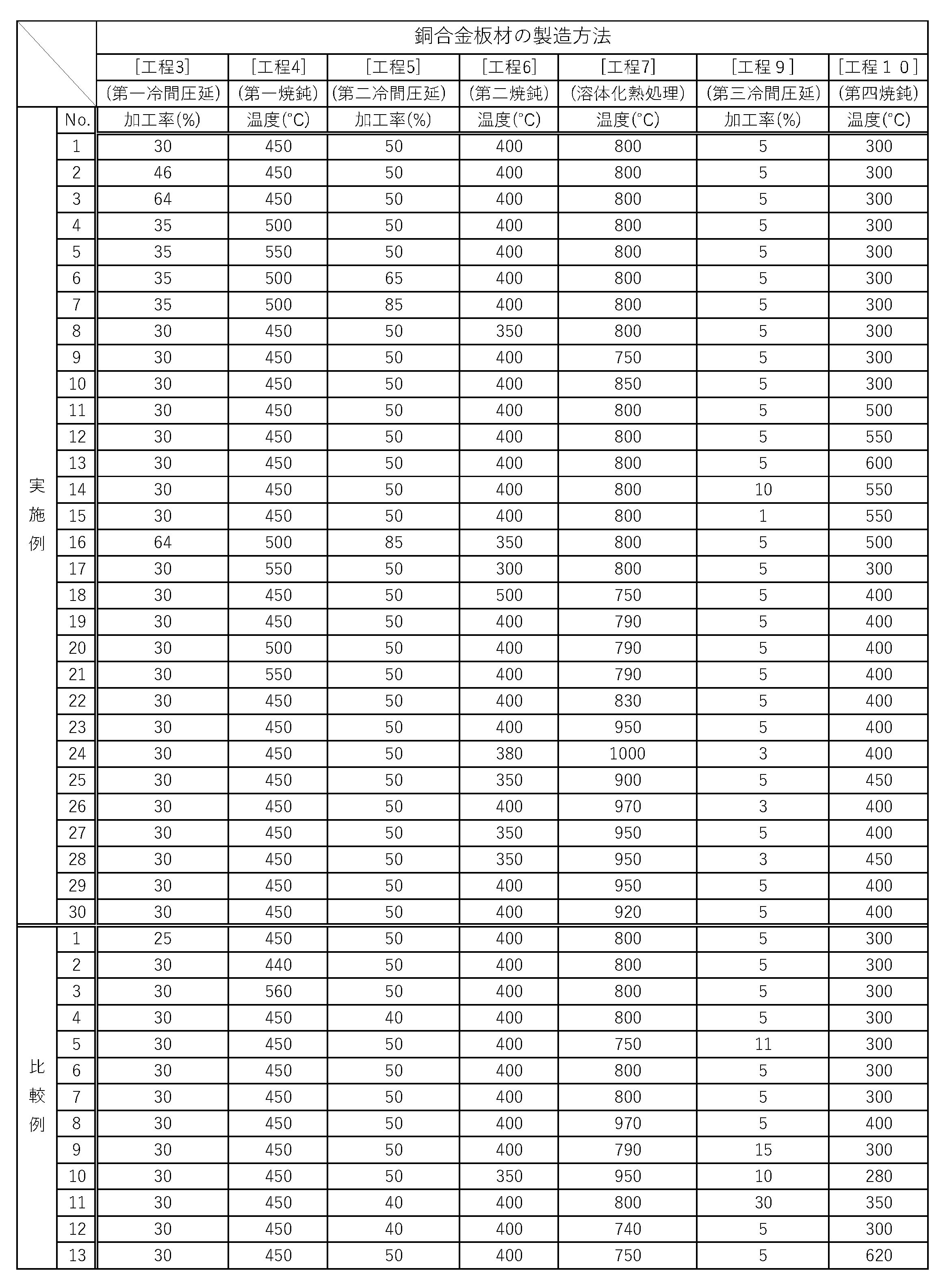
- Step 3 A first cold rolling step was performed in which the material was rolled so that the longitudinal direction of the material was the rolling direction.
- the rolled material after the first cold rolling step [step 3] is subjected to the first annealing step [step 4] in which heat treatment is performed at the attained temperature shown in Table 2 and the holding time for 2 hours. Then, the second cold-rolling step [step 5] was carried out at the reduction rate shown in Table 2, in which the rolled material was rolled so that its longitudinal direction was the rolling direction.
- the rolled material after the second cold rolling step [step 5] is subjected to the second annealing step [step 6] in which heat treatment is performed at the reached temperature shown in Table 2 and for a holding time of 2 hours. was immediately cooled to room temperature by water cooling.
- the rolled material after cooling is subjected to a solution heat treatment step [step 7] in which heat treatment is performed at the reached temperature shown in Table 2 and a holding time of 30 seconds.
- An aging heat treatment step [step 8] was performed in which heat treatment was performed for a holding time of 6 hours.
- a third cold rolling step [step] in which the rolled material after the aging heat treatment step [step 8] is rolled so that the longitudinal direction is in the rolling direction under the conditions of the reduction rate described in Table 2. 9], followed by a fourth annealing step [step 10] in which heat treatment is performed at the attained temperature shown in Table 2 and for a holding time of 4 hours.
- the plate surfaces of Examples 1 to 30 and Comparative Examples 1 to 13 were mirror-finished by electropolishing and used as measurement samples.
- a 1000 ⁇ m ⁇ 1000 ⁇ m visual field area of a mirror-finished measurement sample is measured, and a step size of 0.5 ⁇ m is used, and an EBSD detector attached to a high-resolution scanning analytical electron microscope (manufactured by JEOL Ltd., JSM-7001FA) is used.
- the crystal orientation data were measured continuously. Crystal orientation analysis data was calculated using analysis software (manufactured by TSL, OIM Analysis) for the crystal orientation data obtained by the measurement. From the calculated crystal orientation analysis data, the area ratio of crystal grains having R orientation and the area ratio of crystal grains having Cube orientation were obtained. Subsequently, using the analysis software described above, the average KAM value of the measurement region was calculated with a crystal misorientation of 15° or more as a boundary. Measurement points with a CI value of 0.1 or more were analyzed.
- Tensile strength was adopted as an index indicating the rigidity (strength) of the copper alloy sheet material, and the rigidity (strength) of Examples 1 to 30 and Comparative Examples 1 to 13 was evaluated by measuring the tensile strength.
- the tensile strength was measured using two test pieces of No. 13B specified in JIS Z2241, which were cut out from the test material so that the direction parallel to the rolling direction was the longitudinal direction. The average value of the tensile strength obtained from the test pieces was used as the measured value. Note that in this example, the tensile strength of the copper alloy sheet material of 500 MPa or more was regarded as a passing level.
- ⁇ Measurement of conductivity> The distance between the terminals was set to 100 mm, and the specific resistance was measured twice by the four-terminal method in a constant temperature bath kept at 20 ° C. ( ⁇ 0.5 ° C.), the average value was calculated, and this value was used as the conductivity. . Note that in this example, a passing level was defined when the electrical conductivity of the copper alloy sheet material was 30% IACS (International Annealed Copper Standard) or higher.
- a blank having a diameter of 61 mm was produced by press punching from each of Examples 1 to 30 and Comparative Examples 1 to 13 as a plate material having a thickness of 0.50 mm.
- This blank was drawn into a cup shape with a punch having a diameter of 33 mm using a sheet forming tester manufactured by Eriksen.
- the drawing was performed using two types of punches, one having a radius of curvature R of the corner (shoulder) of the tip of 0.50 mm and the other having a radius of curvature R of 0.75 mm.
- the drawing was performed by applying lubricating oil (trade name: Pleton R-303P, manufactured by Sugimura Chemical Industry Co., Ltd.) to the plate.
- the height from the crest to the valley of the undulations of the obtained cup rim was measured. Evaluation of the height difference of the undulation at this time (waviness evaluation) and evaluation of the curvature radius R of the corner portion of the punch tip (punch R evaluation) were performed according to the following criteria. If the waviness is too low, it will be difficult to leave the drawing bridge, and if the waviness is too high, the drawn shape will be damaged. .
- [Average height difference of undulation (mm)] [Average peak height (mm)] ⁇ [Average valley height (mm)] Equation (2)
- the peak height means the height when measuring from the bottom of the cup formed by drawing to the peak position of the undulation formed on the upper edge of the cup, and the valley height is formed by drawing. It means the height when measuring from the bottom of the molded cup to the trough position of the undulation formed on the upper edge of the cup.
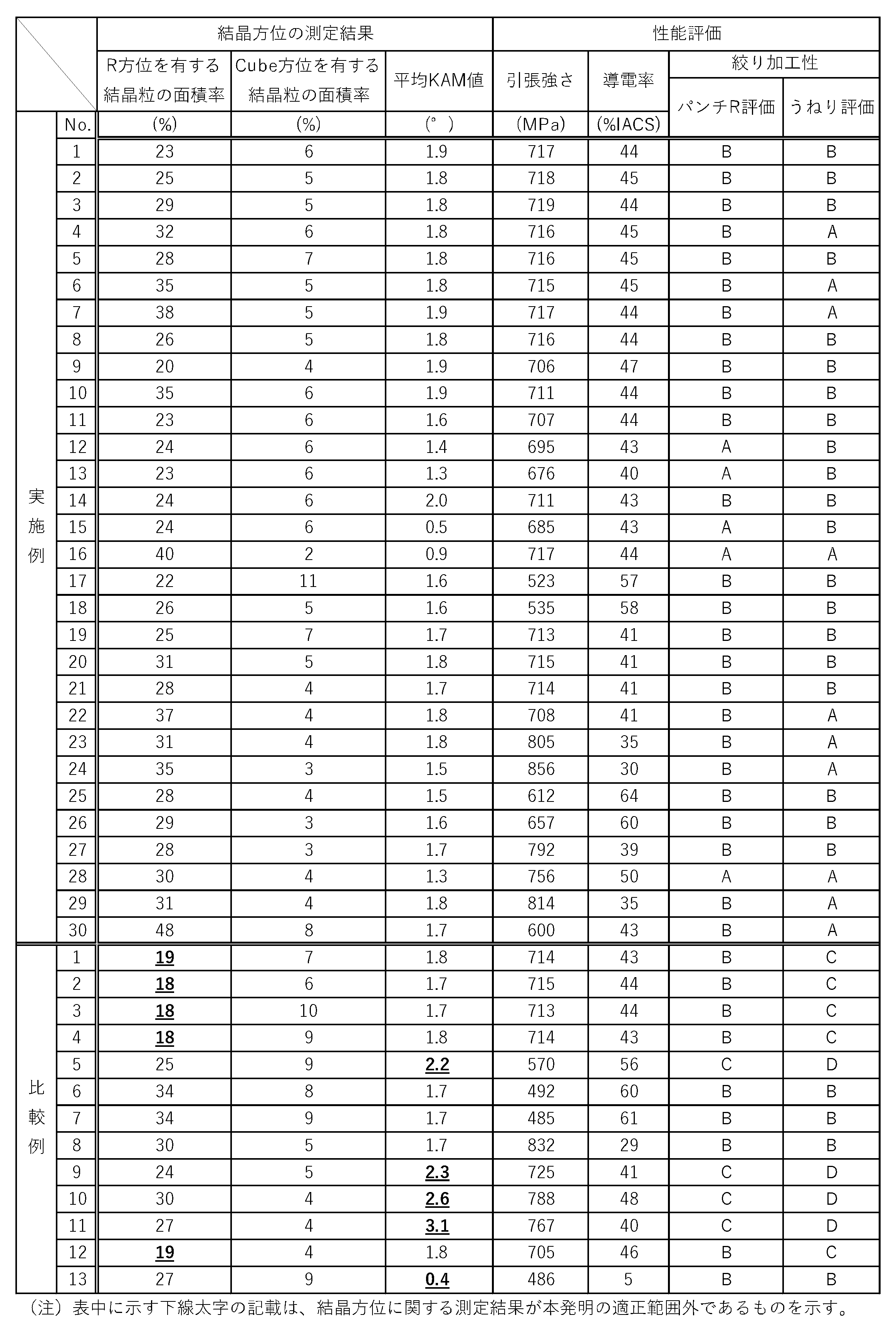
- Table 3 shows the results of the area ratio of R-oriented crystal grains, the area ratio of Cube-oriented crystal grains, the average KAM value, the tensile strength, the electrical conductivity, the waviness evaluation, and the punch R evaluation.
- the alloy composition is within the appropriate range of the present invention, the area ratio of the crystal grains having the R orientation is 20 to 50%, and the average KAM value is 0.5 to 2.0. %, the punch R evaluation and waviness evaluation were both "A (excellent)” or "B (good)", and the copper alloy sheet material was excellent in drawability. .
- Examples 1 to 30 had a tensile strength of 500 MPa or more and an electrical conductivity of 30% IACS or greater, and were copper alloy sheet materials excellent in tensile strength and electrical conductivity. From this, it is considered that Examples 1 to 30 are suitable as materials for electronic parts.
- Examples 1 to 30 in particular, Examples 12, 13, 15, 16, and 28 all had an average KAM value of 0.5 to 1.4, which is the present invention. , the punch R evaluation was "A (excellent)".
- Example 30 the area ratio of crystal grains having the R orientation was as large as 30 or more, and the waviness evaluation was "A (excellent)".
- the area ratio of crystal grains having the R orientation and the average KAM value were within particularly preferable numerical ranges, and both the punch R evaluation and waviness evaluation were "A (excellent)".
- Example 28 contains an appropriate amount of Fe as an optional additive element, and the area ratio of crystal grains having R orientation and the average KAM value are also within appropriate ranges. , conductivity, and drawability were the best.
- Examples 1 to 30 have a tensile strength of 500 MPa or more and are excellent as copper alloy sheet materials applied to drawn parts, but there are differences in tensile strength due to differences in alloy composition and manufacturing process. rice field. Those having a relatively low tensile strength (less than 600 MPa) are considered particularly suitable for drawn parts such as camera module cases, battery cases, or shield cases. On the other hand, those having a relatively high tensile strength (600 MPa or more) are considered to be particularly suitable for drawn parts such as connector hold-downs or shells.
- 600 MPa or more are considered to be particularly suitable for drawn parts such as connector hold-downs or shells.
- An appropriate copper alloy sheet material can be selected and used according to the performance required by each electronic component.
- Comparative Example 6 the Ni content is less than the range of the present invention, and in Comparative Example 7, the Si content is less than the range of the present invention. was rather lacking.
- Comparative Example 8 the total content of Ni and Co was larger than the range of the present invention, so the electrical conductivity was not at an acceptable level.
- Comparative Example 13 has an average KAM value smaller than the range of the present invention, so it can be seen that the tensile strength and electrical conductivity are not at acceptable levels.
- the copper alloy sheet material of the present invention has high strength and high conductivity by controlling the alloy composition, the area ratio of the crystal grains having the R orientation, and the average KAM value within the ranges of the present invention.
Landscapes
- Chemical & Material Sciences (AREA)
- Engineering & Computer Science (AREA)
- Materials Engineering (AREA)
- Mechanical Engineering (AREA)
- Metallurgy (AREA)
- Organic Chemistry (AREA)
- Physics & Mathematics (AREA)
- Thermal Sciences (AREA)
- Crystallography & Structural Chemistry (AREA)
- Conductive Materials (AREA)
Abstract
Description
本実施形態に係る銅合金板材は、NiとCoのうちの少なくとも一方の成分を1.00~5.00質量%、およびSiを0.20~1.50質量%含有し、残部がCuおよび不可避不純物である組成を有する銅合金からなる。
Ni(ニッケル)とCo(コバルト)は、ともに銅合金板材の強度を高める作用を有する重要な成分である。この作用を発揮させるために、NiとCoのうち少なくとも一方の含有量は、これらの合計で1.00質量%以上とする必要がある。また、前記含有量が合計で5.00質量%以下であれば、導電率をさほど低下させることなく、電子部品の材料として適した導電率を維持することができる。このため、NiとCoのうちの少なくとも一方の成分の含有量は、合計で1.00~5.00質量%とする。なお、NiとCoのうちの少なくとも一方の成分の含有量は、高強度と高導電率の双方をバランスよく両立させる観点から、合計で1.50~4.00質量%とすることが好ましく、より好ましくは、合計で2.00~3.50質量%とする。
Si(ケイ素)は、銅合金板材の強度を高める作用を有する重要な成分である。この作用を発揮させるために、Siの含有量は、0.20質量%以上とする必要がある。また、Si含有量が1.50質量%以下であれば、Si成分を起点とするクラック発生のおそれがなく、導電率をさほど低下させることなく、電子部品の材料として適した導電率を維持することができる。このため、Si含有量は、0.20~1.50質量%とする。なお、Si含有量は、高強度と高導電率の双方をバランスよく両立させる観点から、0.40~1.00質量%であることが好ましく、より好ましくは0.50~0.80質量%とする。
銅合金板材を構成する銅合金は、上記した成分以外は、残部がCu(銅)および不可避不純物である合金組成を有する。なお、ここでいう「不可避不純物」とは、おおむね金属製品において、原料中に存在するものや、製造工程において不可避的に混入するもので、本来は不要なものであるが微量であり、金属製品の特性に影響を及ぼさないため許容されている不純物である。不可避不純物として挙げられる成分としては、例えば、S(硫黄)、C(炭素)、O(酸素)などの非金属元素、およびSb(アンチモン)などの金属元素などが挙げられる。不可避不純物は、含有量が多いと導電率を低下させる要因にもなりうるため、導電率の低下を考慮して不可避不純物の含有量を抑制することが好ましい。なお、不可避不純物の銅合金全体に対する含有量の上限は、例えば上記成分ごとに0.05質量%、上記成分の総量で0.20質量%とすることができる。
本実施形態の銅合金板材は、主成分のCuに加え、NiとCoのうちの少なくとも一方の成分とSiを必須含有成分とするが、必要に応じて、任意添加成分として、さらにMg、Sn、Zn、Cr、Zr、およびFeからなる群から選ばれる少なくとも1種の成分を、合計で0.10~1.00質量%含有することができる。
Mg(マグネシウム)は、耐応力緩和特性を向上させる作用を有する成分である。この作用を発揮させるには、Mg含有量を0.10質量%以上とすることが好ましい。一方、Mg含有量が0.30質量%よりも多いと、導電率が低下する傾向があるため、Mg含有量は、0.10~0.30質量%とすることが好ましい。
Sn(スズ)は、耐応力緩和特性を向上させる作用を有する成分である。この作用を発揮させるには、Sn含有量を0.10質量%以上とすることが好ましい。一方、Sn含有量が0.30質量%よりも多いと、導電率が低下する傾向があるため、Sn含有量は、0.10~0.30質量%とすることが好ましい。
Zn(亜鉛)は、Snめっきの密着性やマイグレーション特性を改善する作用を有する成分である。この作用を発揮させるには、Zn含有量を0.10質量%以上とすることが好ましい。一方、Zn含有量が0.50質量%よりも多いと、導電率が低下する傾向があるため、Zn含有量は、0.10~0.50質量%とすることが好ましい。
Cr(クロム)は、溶体化熱処理における結晶粒の粗大化を抑制し、粒径の制御を容易にする作用を有する成分である。この作用を発揮させるには、Cr含有量を0.05質量%以上とすることが好ましい。一方、Cr含有量が0.30質量%を超えると、鋳造時にCrを含有する粗大な晶出物を生じて、クラックの起点が形成され易くなるため、Cr含有量は、0.05~0.30質量%とすることが好ましい。
Zr(ジルコニウム)は、材料中に固溶し、材料の再結晶温度を上昇させることで溶体化熱処理における再結晶粒の成長を抑制する作用を有する成分である。この作用を発揮させるには、Zr含有量を0.05質量%以上とすることが好ましい。一方、Zr含有量が0.20質量%を超えると、鋳造時に粗大な晶出物を生じてプレス加工時の破断の起点になるおそれが高まることから、Zr含有量は、0.05~0.20質量%とすることが好ましい。
Fe(鉄)は、溶体化熱処理における結晶粒の粗大化を抑制し、粒径の制御を容易にする作用を有する成分である。この作用を発揮させるには、Fe含有量を0.05質量%以上とすることが好ましい。一方、Fe含有量が0.30質量%を超えると、鋳造時にFeを含有する粗大な晶出物を生じて、クラックの起点が形成され易くなるため、Fe含有量は、0.05~0.30質量%とすることが好ましい。
本実施形態に係る銅合金板材は、銅合金を構成する結晶粒において、特定の結晶方位を制御することによって、絞り加工性を向上させたものである。具体的には、本実施形態に係る銅合金板材は、EBSD法によって測定される、R方位{1 2 4}<2 1 -1>を有する結晶粒の面積率が20~50%であり、かつ平均KAM値が0.5~2.0°である。これらが同時に満たされることにより、相乗効果により銅合金板材の絞り加工性が大きく向上し、例えば小さな曲率半径を含む、難形状の厳しい加工条件の場合においても、優れた精度で絞り加工を行うことが可能となるため、有用性が飛躍的に向上する。
「EBSD」とは、Electron BackScatter Diffractionの略で、走査型電子顕微鏡(SEM)内で試料に電子線を照射したときに生じる反射電子菊池線回折を利用した結晶方位解析技術のことである。
R方位は、{1 2 4}<2 1 -1>と表記される結晶方位である。本実施形態では、EBSD法によって測定されるR方位を有する結晶粒の面積率は20~50%であることが必要である。R方位を有する結晶粒を集積し、R方位を有する結晶粒の面積率を上記の範囲内とすることで順送プレス絞り加工時に、局所的に面積の小さいフランジを確実に残すことができ、その結果、製品(絞り加工部品)の歩留まりが向上する。R方位を有する結晶粒の面積率が20%未満の場合は、適度なフランジを残しづらく、順送プレス加工時にフランジとブリッジの間での破断が起こり易くなり、製品(絞り加工部品)の歩留まりが低下する。一方、R方位を有する結晶粒の面積率が50%超えの場合は、フランジ面積が大きくなりすぎて、材料ロスが多くなる結果、製品(絞り加工部品)の歩留まりが低下する。なお、R方位を有する結晶粒の面積率は、25~45%であることが好ましく、30~40%であることがさらに好ましい。
KAM値とは、Kernel Average Misorientation値の略称であり、結晶粒内の各ピクセルの結晶方位をEBSD法によって測定し、測定した各ピクセルと、結晶粒界を超えない範囲(すなわち15°未満)に存在し隣接するピクセルとの方位差の平均値を算出したものである。また本実施形態では、銅合金板材の任意の1視野において測定面を設定し、EBSD法による測定を行ない、測定面内の複数の測定点から算出した平均値を平均KAM値とする。
Cube方位は、{1 0 0}<0 0 1>と表記される結晶方位である。本実施形態では、上記のR方位および平均KAM値の制御に加えて、EBSD法によって測定されるCube方位を有する結晶粒の面積率が、10%以下に制御されることが好ましい。Cube方位を有する結晶粒の面積率が10%より大きい場合は、絞り加工後のうねりの高低差が小さくなる。この結果、適度なフランジを残しづらくなり、順送プレス加工時にフランジとブリッジの間での破断が起こり易くなり、製品歩留まりの低下を招くおそれがある。また、フランジとブリッジの間での破断を防ぐために、あえてフランジ面積を大きくすることも可能であるが、その場合は、材料ロスが増えるため好ましくない。なお、Cube方位を有する結晶粒の面積率は、2~8%であることがより好ましい。
R方位およびCube方位以外の方位を有する結晶粒の面積率は、特に限定されないが、例えば、Brass方位{1 1 0}<1 -1 2>を有する結晶粒の面積率は5.0%未満、Goss方位{1 1 0}<0 0 1>を有する結晶粒の面積率は2.0%未満、および/またはCopper方位{1 1 2}<1 1 -1>を有する結晶粒の面積率は5.0%未満に制御されることが好ましい。
本実施形態に係る銅合金板材は、合金組成や製造プロセスを組み合わせて制御することによって製造することが可能である。熱伝導性(導電性)、高い剛性(強度)に加えて、優れた絞り加工性を得ることが可能な製造プロセスの一例として、限定されないが以下の方法を挙げることができる。
溶解鋳造工程[工程1]は、上記の合金組成を有する銅合金素材を溶融させ、これを鋳造することによって、所定形状(例えば厚さ30mm、幅100mm、長さ150mm)の鋳塊(インゴット)を作製する工程である。[工程1]は、高周波溶解炉を用いて、大気中、不活性ガス雰囲気中または真空中で、銅合金素材を溶融および鋳造することが好ましい。なお、銅合金素材の合金組成は、製造の各工程において、添加成分によっては溶解炉に付着したり揮発したりして、製造される銅合金板材の合金組成と必ずしも完全に一致しない場合があるが、銅合金板材の合金組成と実質的に同じ合金組成を有している。
再熱・熱間圧延工程[工程2]では、まず上記の鋳塊を800~1000℃で1~6時間保持し熱処理(再熱)を行なう。この[工程2]において、鋳塊に含有される粗大な凝固偏析や晶出物は、できるだけ母相に固溶させて小さくし、可能な限り無くして均質化する。均質化した直後に所定の厚さになるまで熱間圧延を行なう。熱間圧延の温度は、700℃以上であり、上記の熱処理(再熱)時と同じ800~1000℃の範囲とすることもでき、熱間圧延における加工率は50~90%の範囲で行なうことができる。熱間圧延終了後は直ちに冷却する。なお、熱延材の表面に酸化スケールが多い場合は、0.5~4.0mmの面削を行ない、酸化スケールを除去することが好ましい。
第一冷間圧延工程[工程3]は、[工程2]を行なった後の熱延材に、冷間圧延を施す工程である。[工程3]における圧延は、製品板厚に合わせて任意の圧下率で行なうことができる。この[工程3]における加工率は、30%以上とすることが好ましく、40%以上とすることがより好ましく、50%以上とすることがさらに好ましい。なお加工率の上限値は特に限定されないが、例えば99.9%以下とすることができる。加工率が30%未満の場合は、その後に行なう第一焼鈍工程[工程4]において生成される析出物の量が少なく、溶体化熱処理工程[工程7]でのR方位を有する結晶粒の集積度が低下する傾向がある。
第一焼鈍工程[工程4]は、第一冷間圧延工程[工程3]を行なった後の冷延材に対して、合金組成に応じて熱処理を施す工程である。この[工程4]での焼鈍条件は、到達温度を450~550℃、保持時間を1~6時間とすることができる。到達温度が450℃未満の場合は、その後に行なう溶体化熱処理工程[工程7]でのR方位を有する結晶粒の集積度が低下する。またこの工程における析出物の量、および/またはサイズが、溶体化熱処理工程[工程7]でのR方位を有する結晶粒の集積度に影響していると推定される。一方、到達温度が550℃を超える場合は、母相の再結晶化が進み、Cube方位の面積率が増加し、絞り加工性が低下する傾向がある。
第二冷間圧延工程[工程5]は、第一冷間圧延工程[工程4]を行なった後の材料に対して、圧延ワークロールを用いてさらに冷間圧延を施す工程である。この[工程5]における加工率は、50%以上とすることが好ましく、60%以上とすることがより好ましく、70%以上とすることがさらに好ましい。なお加工率の上限値は特に限定されないが、例えば99.9%以下とすることができる。加工率が50%未満の場合は、その後に行なう溶体化熱処理工程[工程7]でのR方位を有する結晶粒の集積度が低下する傾向がある。
第二焼鈍工程[工程6]は、第二冷間圧延工程[工程5]を行なった後の冷延材に対して熱処理を施して再結晶させる焼鈍し、歪量を調製する工程である。ここで[工程6]における熱処理の条件は、例えば、到達温度が300~400℃、かつ到達温度での保持時間が1~6時間にすることができる。到達温度が300℃未満の場合は、歪量が多くなり、その後に行なう溶体化熱処理工程[工程7]でのR方位を有する結晶粒の集積度が低下する傾向がある。一方、到達温度が400℃を超える場合は、部分的な再結晶化が進み、その後に行なう溶体化熱処理工程[工程7]でのR方位を有する結晶粒の集積度が低下する傾向がある。
溶体化熱処理工程[工程7]は、第二焼鈍工程[工程6]を行なった後の材料に対して、熱処理を行なう工程である。この[工程7]での焼鈍条件は、到達温度を750~1000℃、保持時間を10~60秒とすることができる。到達温度が750℃未満の場合は、R方位を有する結晶粒の集積度が低下する傾向がある。一方、到達温度が1000℃を超える場合は、結晶粒が粗大化し、強度が低下し、また絞り加工部品の外観を損なうおそれがある。なお、その後に行なう時効熱処理工程[工程8]での析出強化を得るために、熱処理後には直ちに50℃/s以上で急冷することが好ましい。
時効熱処理工程[工程8]は、溶体化熱処理工程[工程7]を行なった後の材料に対して、熱処理を行なう工程である。この[工程8]では、例えば、400~600℃で1~6時間の熱処理を行なう。400℃未満の場合、または600℃を超える場合、充分な析出強化が得られない。
第三冷間圧延工程[工程9]は、時効熱処理工程[工程8]を行なった後の材料に対して、さらに冷間圧延を施す工程である。[工程9]における加工率は、1~10%であることが好ましく、1~5%であることがさらに好ましい。加工率が1%未満の場合は、強度向上の効果が小さい。一方、加工率が10%を超える場合、平均KAM値が大きくなり、絞り加工性が低下する。
第四焼鈍工程[工程10]は、第三冷間圧延工程[工程9]を行なった後の材料に対して熱処理を施して、歪取り焼鈍を行なう。この[工程10]での焼鈍条件は、到達温度を300~600℃、保持時間を10~60秒とすることが好ましい。到達温度が300℃未満の場合は、平均KAM値が高くなり、絞り加工性が低下する。600℃を超える場合は析出物の再固溶により、強度と導電性が低下する。到達温度は、350~550℃がさらに好ましく、400~500℃が特に好ましい。
本実施形態に係る銅合金板材は、R方位を有する結晶粒および平均KAM値を制御することによって、製品(絞り加工部品)の歩留まりを向上したものであり、絞り加工部品を作製するための素材として用いることに適したものである。また、本実施形態に係る銅合金板材は、優れた絞り加工性と同時に、高い強度と導電性を有するため、例えば、電子機器部品(コネクタ、リードフレーム、リレー、スイッチ、ソケット、シールドケース、シールドキャン、およびカメラモジュールなど)、液晶や有機ELディスプレイ用部品(放熱部品、およびバッテリーなど)、自動車車載用部品(コネクタ、シールドケース、およびシールドキャンなど)など絞り加工部品の材料として好適に用いることができる。特にコネクタのホールドダウンまたはシェル、カメラモジュールケース、バッテリーケース、あるいはシールドケースなどの絞り加工部品の材料として最適である。
表1に示す合金組成を有する種々の銅合金素材を溶解し、これを大気雰囲気で冷却して鋳造する溶解鋳造工程[工程1]を行なって鋳塊を得た。

上記のとおり製造した実施例1~30および比較例1~13に対して、EBSD法による測定を行ない、R方位を有する結晶粒の面積率、Cube方位を有する結晶粒の面積率、および平均KAM値を得た。
銅合金板材の剛性(強度)を示す指標として引張強さを採用し、実施例1~30および比較例1~13の剛性(強度)について、引張強さを測定することで評価した。引張強さの測定は、圧延方向に対して平行な方向が長手方向になるように供試材を切り出した、JIS Z2241に規定されている13B号の2本の試験片で行ない、2本の試験片から得られた引張強さの平均値を測定値とした。なお本実施例では、銅合金板材の引張強さが500MPa以上を合格レベルとした。
端子間距離を100mmとし、20℃(±0.5℃)に保たれた恒温槽中で四端子法により比抵抗を2回測定し、この平均値を算出し、この値を導電率とした。なお本実施例では、銅合金板材の導電率が30%IACS(International Annealed Copper Standard)以上である場合を合格レベルとした。
実施例1~30および比較例1~13を板厚0.50mmの板材として、プレス打ち抜きで直径61mmのブランクを作製した。このブランクに対してエリクセン社製薄板成形試験機を用いて、直径33mmのパンチでカップ形状に絞り加工を行なった。また、絞り加工は、先端の角部(肩部)の曲率半径Rが0.50mmであるパンチと、0.75mmであるパンチの2種類のパンチを使用して行った。なお絞り加工は、潤滑油(商品名:プレトンR-303P、スギムラ化学工業社製)を板材に塗布して行なった。得られたカップ縁のうねりにおける山から谷までの高さ(うねりの高低差)をそれぞれ測定した。このときのうねりの高低差の評価(うねり評価)、およびパンチ先端のコーナー部の曲率半径Rの評価(パンチR評価)を以下の基準で行なった。なお、うねり評価の判断基準は、うねりが低すぎると絞りブリッジを残しづらく、高すぎると絞り形状を損なうため、うねりの高低差が小さすぎても大きすぎても絞り加工性が劣ると判断した。
A(優):うねりの高低差の平均が0.75mm以上1.25mm未満の場合
B(良):うねりの高低差の平均が0.25mm以上0.75mm未満の場合
C(不可):うねりの高低差の平均が0.25mm未満または1.25mm以上の場合
D(破断):カップ縁のうねりが破断して測定不可の場合
なお、うねりの高低差の平均は、下記式(2)で算出されるものである。
なお、山高さは、絞り加工して成形されたカップの底からカップ上縁に形成されるうねりの頂点位置までを測定したときの高さを意味し、谷高さは、絞り加工して成形されたカップの底からカップ上縁に形成されるうねりの谷位置までを測定したときの高さを意味する。
A(優):先端肩部の曲率半径Rが0.75mmであるパンチを用いた絞り加工条件だけではなく、先端肩部の曲率半径Rが0.50mmであるパンチを用いた厳しい絞り加工条件でも、破断や側壁のシワが発生することなく、良好な絞り加工部品が試作できた場合
B(良):上記A(優)よりは評価が劣るものの、先端肩部の曲率半径Rが0.75mmであるパンチを用いた絞り加工条件では、破断や側壁のシワが発生することなく、良好な絞り加工部品が試作できた場合
C(不可):先端肩部の曲率半径Rが0.75mmであるパンチを用いた絞り加工条件で、絞り加工部品に破断または側壁のシワが発生した場合
R方位を有する結晶粒の面積率、Cube方位を有する結晶粒の面積率、平均KAM値、引張強さ、導電率、うねり評価、およびパンチR評価の結果を表3に示す。
Claims (5)
- NiとCoのうちの少なくとも一方の成分を、合計で1.00~5.00質量%、およびSiを0.20~1.50質量%含有し、残部がCuおよび不可避不純物である組成を有し、
EBSD法によって測定される、R方位{1 2 4}<2 1 -1>を有する結晶粒の面積率が20~50%であり、かつ平均KAM値が0.5~2.0°である銅合金板材。 - EBSD法で測定されるCube方位{1 0 0}<0 0 1>を有する結晶粒の面積率が10%以下である、請求項1に記載の銅合金板材。
- Mg、Sn、Zn、Cr、ZrおよびFeからなる群から選択される少なくとも1種の成分を合計で0.10~1.00質量%含有する、請求項1または2に記載の銅合金板材。
- 絞り加工部品を作製するための素材として用いる請求項1~3のいずれかに記載の銅合金板材。
- 請求項1~3のいずれかに記載の銅合金板材を用いて作製された絞り加工部品。
Priority Applications (3)
| Application Number | Priority Date | Filing Date | Title |
|---|---|---|---|
| CN202280075127.2A CN118234880A (zh) | 2022-02-04 | 2022-12-22 | 铜合金板材、及使用铜合金板材而制得的引伸加工零件 |
| KR1020247017798A KR20240124905A (ko) | 2022-02-04 | 2022-12-22 | 구리 합금 판재 및 구리 합금 판재를 사용하여 제작된 드로잉 가공 부품 |
| JP2023515176A JP7328472B1 (ja) | 2022-02-04 | 2022-12-22 | 銅合金板材、および銅合金板材を用いて作製された絞り加工部品 |
Applications Claiming Priority (2)
| Application Number | Priority Date | Filing Date | Title |
|---|---|---|---|
| JP2022016518 | 2022-02-04 | ||
| JP2022-016518 | 2022-02-04 |
Publications (1)
| Publication Number | Publication Date |
|---|---|
| WO2023149121A1 true WO2023149121A1 (ja) | 2023-08-10 |
Family
ID=87552244
Family Applications (1)
| Application Number | Title | Priority Date | Filing Date |
|---|---|---|---|
| PCT/JP2022/047421 Ceased WO2023149121A1 (ja) | 2022-02-04 | 2022-12-22 | 銅合金板材、および銅合金板材を用いて作製された絞り加工部品 |
Country Status (5)
| Country | Link |
|---|---|
| JP (1) | JP7328472B1 (ja) |
| KR (1) | KR20240124905A (ja) |
| CN (1) | CN118234880A (ja) |
| TW (1) | TW202332784A (ja) |
| WO (1) | WO2023149121A1 (ja) |
Cited By (1)
| Publication number | Priority date | Publication date | Assignee | Title |
|---|---|---|---|---|
| WO2025120905A1 (ja) * | 2023-12-07 | 2025-06-12 | Jx金属株式会社 | 銅合金板、電子部品及び銅合金板の製造方法 |
Families Citing this family (3)
| Publication number | Priority date | Publication date | Assignee | Title |
|---|---|---|---|---|
| WO2025079295A1 (ja) * | 2023-10-10 | 2025-04-17 | 古河電気工業株式会社 | 銅合金板材、曲げ加工品および絞り加工品 |
| WO2025204142A1 (ja) * | 2024-03-29 | 2025-10-02 | 株式会社フジクラ | 酸化物超電導線材、超電導コイルおよび超電導導体 |
| WO2025204143A1 (ja) * | 2024-03-29 | 2025-10-02 | 株式会社フジクラ | 酸化物超電導線材、超電導コイルおよび超電導導体 |
Citations (4)
| Publication number | Priority date | Publication date | Assignee | Title |
|---|---|---|---|---|
| JP2012122114A (ja) * | 2010-12-10 | 2012-06-28 | Mitsubishi Shindoh Co Ltd | 深絞り加工性及び耐疲労特性に優れたCu−Ni−Si系銅合金板及びその製造方法 |
| JP2015086416A (ja) * | 2013-10-29 | 2015-05-07 | Jx日鉱日石金属株式会社 | 導電性、耐応力緩和性および成形性に優れる銅合金板 |
| JP2018162510A (ja) * | 2017-03-27 | 2018-10-18 | Jx金属株式会社 | 電子材料用銅合金及び電子部品 |
| WO2020121775A1 (ja) * | 2018-12-13 | 2020-06-18 | 古河電気工業株式会社 | 銅合金板材およびその製造方法ならびに絞り加工品、電気・電子部品用部材、電磁波シールド材および放熱部品 |
Family Cites Families (1)
| Publication number | Priority date | Publication date | Assignee | Title |
|---|---|---|---|---|
| JP7614824B2 (ja) | 2020-01-09 | 2025-01-16 | Dowaメタルテック株式会社 | Cu-Ni-Si系銅合金板材およびその製造方法並びに通電部品 |
-
2022
- 2022-12-22 WO PCT/JP2022/047421 patent/WO2023149121A1/ja not_active Ceased
- 2022-12-22 KR KR1020247017798A patent/KR20240124905A/ko active Pending
- 2022-12-22 JP JP2023515176A patent/JP7328472B1/ja active Active
- 2022-12-22 CN CN202280075127.2A patent/CN118234880A/zh active Pending
- 2022-12-28 TW TW111150341A patent/TW202332784A/zh unknown
Patent Citations (4)
| Publication number | Priority date | Publication date | Assignee | Title |
|---|---|---|---|---|
| JP2012122114A (ja) * | 2010-12-10 | 2012-06-28 | Mitsubishi Shindoh Co Ltd | 深絞り加工性及び耐疲労特性に優れたCu−Ni−Si系銅合金板及びその製造方法 |
| JP2015086416A (ja) * | 2013-10-29 | 2015-05-07 | Jx日鉱日石金属株式会社 | 導電性、耐応力緩和性および成形性に優れる銅合金板 |
| JP2018162510A (ja) * | 2017-03-27 | 2018-10-18 | Jx金属株式会社 | 電子材料用銅合金及び電子部品 |
| WO2020121775A1 (ja) * | 2018-12-13 | 2020-06-18 | 古河電気工業株式会社 | 銅合金板材およびその製造方法ならびに絞り加工品、電気・電子部品用部材、電磁波シールド材および放熱部品 |
Cited By (2)
| Publication number | Priority date | Publication date | Assignee | Title |
|---|---|---|---|---|
| WO2025120905A1 (ja) * | 2023-12-07 | 2025-06-12 | Jx金属株式会社 | 銅合金板、電子部品及び銅合金板の製造方法 |
| JPWO2025120905A1 (ja) * | 2023-12-07 | 2025-06-12 |
Also Published As
| Publication number | Publication date |
|---|---|
| JP7328472B1 (ja) | 2023-08-16 |
| CN118234880A (zh) | 2024-06-21 |
| JPWO2023149121A1 (ja) | 2023-08-10 |
| TW202332784A (zh) | 2023-08-16 |
| KR20240124905A (ko) | 2024-08-19 |
Similar Documents
| Publication | Publication Date | Title |
|---|---|---|
| JP7328472B1 (ja) | 銅合金板材、および銅合金板材を用いて作製された絞り加工部品 | |
| KR101628583B1 (ko) | Cu-Ni-Si 계 합금 및 그 제조 방법 | |
| JP5158909B2 (ja) | 銅合金板材及びその製造方法 | |
| KR101419149B1 (ko) | 구리합금판재 | |
| US10190194B2 (en) | Copper alloy for electronic and electrical equipment, copper alloy thin sheet for electronic and electrical equipment, and conductive component for electronic and electrical equipment, terminal | |
| KR101917416B1 (ko) | 전자 재료용 Cu-Co-Si 계 합금 | |
| CN111788320A (zh) | 电子电气设备用铜合金﹑电子电气设备用铜合金板条材、电子电气设备用组件、端子及汇流排 | |
| CN114302975B (zh) | 电子电气设备用铜合金﹑电子电气设备用铜合金板条材、电子电气设备用组件、端子及汇流排 | |
| JP6306632B2 (ja) | 電子材料用銅合金 | |
| WO2011036804A1 (ja) | 電子材料用Cu-Ni-Si-Co系銅合金及びその製造方法 | |
| KR20160102989A (ko) | 구리합금판재, 커넥터, 및 구리합금판재의 제조방법 | |
| JP2017179493A (ja) | 電子・電気機器用銅合金、電子・電気機器用銅合金塑性加工材、電子・電気機器用部品、端子、及び、バスバー | |
| JP7328471B1 (ja) | 銅合金板材およびその製造方法、ならびに電子部品および絞り加工品 | |
| JP2012193408A (ja) | 曲げ加工性に優れたCu−Ni−Si系合金 | |
| JP6928597B2 (ja) | 銅合金板材およびその製造方法ならびに絞り加工品、電気・電子部品用部材、電磁波シールド材および放熱部品 | |
| JP6542817B2 (ja) | 電子材料用銅合金 | |
| CN114867875B (zh) | 铜合金板材及其制造方法、以及电气·电子部件用构件 | |
| WO2023149312A1 (ja) | 電子材料用銅合金及び電子部品 | |
| JP6310004B2 (ja) | 電子部品用Cu−Co−Ni−Si合金 | |
| WO2024225165A1 (ja) | 銅合金板材、絞り加工用銅合金板材および絞り加工品 | |
| WO2025079295A1 (ja) | 銅合金板材、曲げ加工品および絞り加工品 | |
| CN120390813A (zh) | 铜合金板材、拉深加工用铜合金板材及拉深件 | |
| CN121992246A (zh) | 铜合金板材及拉深加工品 | |
| JP2019077890A (ja) | 電子材料用銅合金 | |
| JP2018145495A (ja) | 電子部品用Cu−Ni−Co−Si合金 |
Legal Events
| Date | Code | Title | Description |
|---|---|---|---|
| WWE | Wipo information: entry into national phase |
Ref document number: 2023515176 Country of ref document: JP |
|
| 121 | Ep: the epo has been informed by wipo that ep was designated in this application |
Ref document number: 22925024 Country of ref document: EP Kind code of ref document: A1 |
|
| WWE | Wipo information: entry into national phase |
Ref document number: 202280075127.2 Country of ref document: CN |
|
| NENP | Non-entry into the national phase |
Ref country code: DE |
|
| 122 | Ep: pct application non-entry in european phase |
Ref document number: 22925024 Country of ref document: EP Kind code of ref document: A1 |