WO2023149081A1 - Semiconductor laser element - Google Patents
Semiconductor laser element Download PDFInfo
- Publication number
- WO2023149081A1 WO2023149081A1 PCT/JP2022/045514 JP2022045514W WO2023149081A1 WO 2023149081 A1 WO2023149081 A1 WO 2023149081A1 JP 2022045514 W JP2022045514 W JP 2022045514W WO 2023149081 A1 WO2023149081 A1 WO 2023149081A1
- Authority
- WO
- WIPO (PCT)
- Prior art keywords
- layer
- semiconductor laser
- laser device
- semiconductor
- output
- Prior art date
Links
Images

Classifications
-
- H—ELECTRICITY
- H01—ELECTRIC ELEMENTS
- H01S—DEVICES USING THE PROCESS OF LIGHT AMPLIFICATION BY STIMULATED EMISSION OF RADIATION [LASER] TO AMPLIFY OR GENERATE LIGHT; DEVICES USING STIMULATED EMISSION OF ELECTROMAGNETIC RADIATION IN WAVE RANGES OTHER THAN OPTICAL
- H01S5/00—Semiconductor lasers
- H01S5/02—Structural details or components not essential to laser action
- H01S5/028—Coatings ; Treatment of the laser facets, e.g. etching, passivation layers or reflecting layers
Definitions
- the present disclosure relates to a semiconductor laser device.
- an external resonance type laser device that includes an external resonator that forms a resonant state of laser light with an optical component such as a diffraction grating that is spaced apart from a semiconductor laser element.
- an optical component such as a diffraction grating that is spaced apart from a semiconductor laser element.
- a high-output and high-quality laser light can be emitted by constructing a synthesizing optical system for synthesizing a plurality of laser lights emitted from a semiconductor laser element in the external cavity.
- the spatial synthesis method is a method of spatially synthesizing a plurality of laser beams without focusing them on the same optical axis.
- the wavelength combining method is a method of condensing a plurality of laser beams having different wavelengths on the same optical axis.
- a wavelength synthesis method is preferable to a spatial synthesis method in which a plurality of optical axes are different from each other.
- a semiconductor laser element having a plurality of light emitting points is adopted as the semiconductor laser element.
- the reflectance of the laser light emitting side facet of the laser array element is required to be 1% or less.
- FIG. 1 is a schematic diagram showing a planar configuration of the multi-wavelength semiconductor laser device of Patent Document 1. As shown in FIG.
- the multi-wavelength semiconductor laser device disclosed in Patent Document 1 has a first light emitting section 11 that emits laser light in the 650 nm band and a second light emitting section 12 that emits laser light in the 780 nm band.
- the multi-wavelength semiconductor laser element also has an emission-side protective layer 14 composed of a plurality of dielectric layers 14A, 14B, and 14C on the laser light emission-side facet.
- the emission-side protective layer 14 reduces the reflectance of the emission-side facet for laser light in a wavelength range including the 650 nm band and the 780 nm band.
- a semiconductor laser device includes a semiconductor laminate that emits laser light; an output-side protective layer disposed on the laser light output-side facet of the semiconductor laminate; a non-emission-side protective layer arranged on an end face opposite to the laser light emission-side end face of the semiconductor laminate and reflecting the laser light; with
- the emission-side protective layer has a control layer that suppresses the reflectance on the emission side with respect to the wavelength of the laser beam to a predetermined value or less,
- the control layer has a strain relief layer that suppresses strain due to thermal expansion of the control layer.
- FIG. 1 is a schematic diagram showing a planar configuration of the multi-wavelength semiconductor laser device of Patent Document 1.
- FIG. 2 is a schematic cross-sectional view showing the semiconductor laser device according to the first embodiment.
- FIG. 3 is a schematic diagram showing a semiconductor laser device including the semiconductor laser element according to the first embodiment.
- FIG. 4 is a schematic cross-sectional view showing a semiconductor laser device according to a second embodiment.
- FIG. 5 is a graph showing the reflectance of the semiconductor laser element on the side of the laser light emitting facet, showing the wavelength characteristics of the reflectance for each type of the emitting facet-side protective layer.
- the structure of the emission-side protective layer of the semiconductor laser element is appropriately adjusted, for example, by increasing the types and thicknesses of the constituent layers, in order to ensure the reliability of the laser light.
- the structure of the output-side protective layer is appropriately adjusted so as to suppress the overall reflectance on the output-side facet including reflection inside the output-side protective layer in order to achieve desired laser characteristics.
- the output-side protective layer includes a layer with a high coefficient of thermal expansion
- the internal stress caused by the thermal expansion of the output-side protective layer may cause peeling of the output-side protective layer or damage to the laser light output-side facet of the multi-wavelength semiconductor laser device. , which may lead to deterioration of laser quality.
- An object of the present disclosure is to provide a semiconductor laser element capable of reducing the reflectance on the laser light emitting end face side and improving the laser quality.
- the terms “upper” and “lower” do not refer to the upward direction (vertical upward) and the downward direction (vertical downward) in absolute spatial recognition, but to the stacking of semiconductor stacks described later. It is used as a term defined by a relative positional relationship based on the stacking order in the configuration. Also, the terms “above” and “below” are used not only when two components are spaced apart from each other and there is another component between the two components, but also when two components are spaced apart from each other. It also applies when they are arranged in contact with each other.
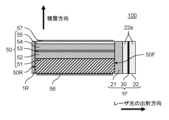
- FIG. 2 is a schematic cross-sectional view showing the semiconductor laser device 100 according to the first embodiment.
- FIG. 2 shows a cross-section of the semiconductor laser element 100 along a plane along the lamination direction of each layer of the semiconductor laminate 50 (described later) and the emission direction of the laser light.
- the semiconductor laser device 100 is a semiconductor light emitting device that emits a plurality of laser beams, a so-called semiconductor laser array.
- the semiconductor laser device 100 is a gallium nitride-based semiconductor laser device, and emits laser light having a wavelength in a band of about 390 nm to 530 nm.
- the semiconductor laser element 100 includes a semiconductor laminate 50, an emitting-side protective layer 1F, and a non-emitting-side protective layer 1R.
- the semiconductor laminate 50 is a laminate of a plurality of semiconductor layers.
- the semiconductor laminate 50 has a substrate 51 , a first semiconductor layer 52 , an active layer 53 , a second semiconductor layer 54 and a contact layer 55 .
- the substrate 51 is a plate-like member that serves as the base material of the semiconductor laminate 50 .
- the substrate 51 is a GaN single crystal substrate.
- the thickness of the substrate 51 is, for example, approximately 100 ⁇ m.
- the material forming the substrate 51 may be single crystal such as Al 2 O 3 (sapphire), SiC, GaAs, or InP. Also, the thickness of the substrate 51 may be, for example, 50 ⁇ m or more and 120 ⁇ m or less.
- the first semiconductor layer 52 is a semiconductor layer formed above the substrate 51 .
- the first semiconductor layer 52 is an n-type semiconductor layer and includes an n-type clad layer.
- the n-type clad layer is a layer made of n-Al 0.2 Ga 0.8 N.
- the thickness of the n-type clad layer is, for example, about 1 ⁇ m.
- the n-type cladding layer may be made of, for example, n-Al x Ga 1-x N (0 ⁇ x ⁇ 1). Also, the thickness of the n-type cladding layer may be, for example, 0.5 ⁇ m or more and 5 ⁇ m or less.
- an n-type Al x InyGa 1-x-yN (0 ⁇ x+y ⁇ 1) guide layer or an undoped Al x InyGa 1-x-yN (0 ⁇ x+y ⁇ 1) guide layer is formed on the n-type cladding layer. may be formed.
- the active layer 53 is a layer formed above the first semiconductor layer 52 .
- the active layer 53 functions as a light emitting layer.
- the active layer 53 has two well layers.
- the active layer 53 is a quantum well active layer in which well layers made of In 0.18 Ga 0.82 N and barrier layers made of GaN are alternately laminated.
- the thickness of the well layer is, for example, approximately 5 nm
- the thickness of the barrier layer is, for example, approximately 10 nm.
- the active layer 53 is composed of a well layer made of InxGa1 -xN (0 ⁇ x ⁇ 1) and AlxInyGa1 -x-yN (0 ⁇ x+y ⁇ 1) . Quantum well active layers in which barrier layers are alternately laminated may be used.
- the active layer 53 may have a guide layer at least one of above and below the quantum well active layer. Although the number of well layers is two in this embodiment, it may be one to four. In addition, the In composition of the well layer may be appropriately selected so that light with a desired wavelength is emitted within the wavelength range of 390 nm or more and 530 nm or less.
- the second semiconductor layer 54 is a semiconductor layer formed above the active layer 53 .
- the second semiconductor layer 54 is a p-type semiconductor layer and includes a p-type clad layer.
- the p-type cladding layer is a superlattice layer in which 100 layers of p-Al 0.2 Ga 0.8 N and 100 layers of GaN are alternately laminated.
- the thickness of the p-Al 0.2 Ga 0.8 N layer is, for example, approximately 3 nm, and the thickness of the GaN layer is, for example, approximately 3 nm.
- the p-type cladding layer may be a layer formed of Al x Ga 1-x N (0 ⁇ x ⁇ 1) instead of the superlattice layer described above.
- the thickness of this layer may be, for example, 0.3 ⁇ m or more and 1 ⁇ m or less.
- the p-type clad layer may be a bulk clad layer made of Al x Ga 1-x N (0 ⁇ x ⁇ 1).
- AlGaN is used as the material of the p-type clad layer.
- the reason is that AlGaN has a refractive index suitable for confining laser light in the active layer 53 .
- Materials other than AlGaN may be used as the material of the p-type cladding layer.
- ITO may be used as the material of the p-type clad layer.
- a material that transmits emitted laser light such as a transparent dielectric oxide such as In 2 O 3 , Ga 2 O 3 , SnO, or InGaO 3 may be used.
- the second semiconductor layer 54 includes a p-type Al x In y Ga 1-x-y N (0 ⁇ x+y ⁇ 1) guide layer and undoped Al x In y Ga 1-x under the p-type cladding layer.
- a plurality of -yN (0 ⁇ x+y ⁇ 1) guide layers may be provided.
- the contact layer 55 is a semiconductor layer formed above the second semiconductor layer 54 and is in ohmic contact with the second electrode 57 .
- the contact layer 55 is a p-type semiconductor layer made of p-GaN.
- the thickness of the contact layer 55 is, for example, approximately 10 nm.
- the material of the contact layer 55 is not limited to p-GaN. Also, the thickness of the contact layer 55 may be, for example, 5 nm or more and 200 nm or less.
- two or more ridges are formed in the second semiconductor layer 54 and contact layer 55 .
- a region of the active layer 53 corresponding to each ridge portion serves as a light emitting point, and laser light is emitted from a plurality of light emitting points.
- a first electrode 56 is arranged as an electrode on the lower main surface of the substrate 51 (that is, the main surface on which the first semiconductor layer 52 and the like are not arranged).
- the first electrode 56 is an n-side electrode and has a laminated structure in which a Ti layer, a Pt layer, and an Au layer are laminated in order from the substrate 51 side.
- the first electrode 56 may have another laminated structure, for example, a laminated structure in which a Ti layer and an Au layer are laminated.
- a second electrode 57 is arranged on the contact layer 55 as an electrode.
- the second electrode 57 has a p-side electrode that makes ohmic contact with the contact layer 55 and a pad electrode that is arranged on the p-side electrode.
- the p-side electrode has a laminated structure in which a Pd layer and a Pt layer are laminated in order from the contact layer 55 side. Also, the configuration of the p-side electrode is not limited to this.
- the p-side electrode may have a single layer structure or a multilayer structure including at least one of a Cr layer, Ti layer, Ni layer, Pd layer, Pt layer and Au layer, for example.
- the p-side electrode may be an ITO layer used as a transparent oxide electrode, an In 2 O 3 layer, a Ga 2 O 3 layer, an SnO layer, or an InGaO 3 layer.
- the pad electrode is a pad-shaped electrode arranged above the p-side electrode.
- the pad electrode has a laminated structure in which layers formed of a Ti layer and an Au layer are laminated in order from the p-side electrode side, and are arranged on the ridge and its periphery.
- the pad electrode may be composed of, for example, only an Au layer, or may have a laminated structure in which a Ti layer, a Pt layer and an Au layer are laminated, or a laminated structure in which a Ni layer and an Au layer are laminated. may be Also, the pad electrode may have a laminated structure in which two or more layers made of another metal are laminated.
- the semiconductor laminate 50 may further include an insulating layer such as an SiO 2 film covering the sidewalls of the ridge.
- Non-emission-side protective layer 1R is a layer arranged on the laser light non-emission-side facet 50R of the semiconductor laminate 50 (hereinafter referred to as "non-emission-side facet 50R").
- the non-emission-side protective layer 1R protects the non-emission-side facet 50R and increases the reflectance of the non-emission side of the semiconductor laminate 50 with respect to laser light to a certain value (eg, 90%) or higher.
- the “reflectance on the non-emission side” means the reflectance that is comprehensively evaluated by combining the non-emission-side end surface 50R and the non-emission-side protective layer 1R.
- the non-emission-side protective layer 1R has a multi-layer structure in which a plurality of pairs of SiO 2 layers and AlO 1-x N x (0 ⁇ x ⁇ 1) layers are laminated.
- the thicknesses of the SiO 2 layer and the AlO 1-x N x (0 ⁇ x ⁇ 1) layer are, for example, SiO 2 layer and AlO 1-x N x (0 ⁇ x ⁇ 1), where ⁇ a is the average wavelength of a plurality of laser beams. ⁇ 1)
- ⁇ a is the average wavelength of a plurality of laser beams.
- ⁇ 1 When the refractive index of each layer is n, it is approximately ⁇ a/(4n).
- the reflectance of the non-emission side with respect to the laser light becomes 90% or more.
- the semiconductor laser device 100 with high slope efficiency and low threshold current can be realized.
- the laminated structure of the non-emitting side protective layer 1R is not limited as long as a desired value of reflectance on the non-emitting side can be obtained.
- the non-emission-side protective layer 1R includes a set of SiO 2 layer and ZrO 2 layer, a set of SiO 2 layer and Ta 2 O 5 layer, a set of SiO 2 layer and AlN layer, a set of SiO 2 layer and TiO 2 layer. , a set of SiO 2 layers and HfO 2 layers, a set of SiO 2 layers and Nb 2 O 5 layers, or a set of SiO 2 layers and Al 2 O 3 layers, etc. good.
- the Al 2 O 3 layer may be used as the low refractive index layer.
- the non-emission-side protective layer 1R may have a single-layer structure or a multi-layer structure including at least one of an oxynitride layer and a nitride layer.
- the emission-side protective layer 1F is a layer arranged on the laser light emission-side facet 50F of the semiconductor laminate 50 (hereinafter referred to as the "emission-side facet 50F").
- the emission-side protective layer 1F protects the emission-side facet 50F and reduces the reflectance of the semiconductor laminate 50 on the emission side of the laser beam.
- the “output-side reflectance” means the reflectance that is comprehensively evaluated by combining the output-side end face 50F and the output-side protective layer 1F.
- the exit-side protective layer 1F includes a barrier layer 21 and a control layer 22.
- the reflectance on the output side may be simply called "reflectance”.
- the barrier layer 21 is arranged in contact with the emission-side end surface 50F.
- the barrier layer 21 has a function of suppressing deterioration of the output-side facet 50 ⁇ /b>F of the semiconductor stacked body 50 .
- the barrier layer 21 is a dielectric layer, specifically an oxynitride layer or a nitride layer.
- the barrier layer 21 is a single layer made of AlO 1-x N x (0 ⁇ x ⁇ 1), for example. Moreover, the thickness of the barrier layer 21 is, for example, about 20 nm.
- the barrier layer 21 may be, for example, an oxynitride layer such as a SiO 1-x N x (0 ⁇ x ⁇ 1) layer, or a nitride layer such as an AlN layer or a SiN layer. may
- the control layer 22 is arranged in contact with the emission-side surface of the barrier layer 21 .
- the control layer 22 has a function of adjusting the reflectance of the output side of the semiconductor laminate 50 . More specifically, the control layer 22 suppresses the reflectance on the emission side to a predetermined value (for example, 1%) or less for each oscillation wavelength of the laser light.
- the control layer 22 has a main control layer 22a that contributes to adjusting the reflectance, and a strain relaxation layer 30 that relaxes the strain of the control layer 22 as a whole.
- the main control layer 22a and the strain relaxation layer 30 are made of different materials.
- the main control layer 22a is a dielectric layer, specifically an oxynitride layer, a nitride layer, or an oxide layer.
- the main control layer 22a is a layer made of Al2O3 , for example.
- the total thickness of the main control layer 22a on both sides of the strain relaxation layer 30 is, for example, about 55 nm.
- the main control layer 22a is an oxynitride layer such as an AlO 1-x N x (0 ⁇ x ⁇ 1) layer or a SiO 1-x N x (0 ⁇ x ⁇ 1) layer, an AlN layer, or an SiN layer. It may be a nitride layer, such as a layer, or an oxide layer, such as TiO 2 layer, Nb 2 O 5 layer, ZrO 2 layer, Ta 2 O 5 layer, or HfO 2 layer. Since the main control layer 22a has such a structure, the reflectance on the output side can be suppressed to 1% or less for each wavelength of laser light. As a result, stable external resonance characteristics can be realized in a laser device including the semiconductor laser element 100 .
- the strain relaxation layer 30 is arranged so as to be inserted at an intermediate position in the control layer 22 in the traveling direction of the laser light. That is, the strain relaxation layer 30 is sandwiched between two main control layers 22a.
- the two main control layers 22a may be made of the same material, or may be made of different materials.
- the strain relaxation layer 30 has a function of suppressing strain due to thermal expansion of the entire emission-side protective layer 1F including the control layer 22. It should be noted that the thermal expansion of the control layer 22 is caused by the heat generated by the emitted laser light.
- the strain relaxation layer 30 is a dielectric layer, and has a smaller thermal expansion coefficient than at least the main control layer 22a.
- the strain relaxation layer 30 is made of a material having the smallest coefficient of thermal expansion among the layers included in the output-side protective layer 1F.
- a material with low light absorption in the wavelength range near the 450 nm band is selected in order to suppress light absorption of laser light.
- the strain relaxation layer 30 is made of SiO2 .
- SiO 2 is a substance with a relatively small thermal expansion coefficient and little light absorption in the vicinity of the 450 nm band. Also, since SiO 2 is an oxide layer, it is less susceptible to the effects of surrounding layers and the outside air.
- ⁇ Action of strain relaxation layer> When a laser beam is emitted from the semiconductor laser element 100, the vicinity of the emission-side facet 50F becomes a high temperature state, and the emission-side protective layer 1F thermally expands. At this time, tensile stress is generated at the interface between the semiconductor laminate 50 and the output-side protective layer 1F. In particular, when a part of the exit-side protective layer 1F includes a layer formed of a material having a large coefficient of thermal expansion, the tensile stress increases.
- the entire output-side protective layer 1F including the control layer 22 can be restrained from being strained due to thermal expansion. More specifically, the thermal expansion of the output-side protective layer 1F can be suppressed, and the tensile stress generated at the interface between the output-side protective layer 1F and the output-side end surface 50F can be reduced.
- SiO 2 forming the strain relaxation layer 30 has a smaller thermal expansion coefficient than Al 2 O 3 or the like forming the main control layer 22a. Therefore, by arranging the strain relaxation layer 30 between the two main control layers 22a (Al 2 O 3 layers), it is possible to effectively suppress strain due to thermal expansion of the output-side protective layer 1F.
- the material for the strain relaxation layer 30 should have a smaller thermal expansion coefficient than the material for the main control layer 22a. It is more desirable if the material of the strain relaxation layer 30 is a material with the smallest coefficient of thermal expansion among the layers included in the output-side protective layer 1F.
- the light absorption is small with respect to the oscillation wavelength of each laser light (for example, the extinction coefficient is 2.0 ⁇ 10 ⁇ 3 or less)
- materials other than SiO 2 may be used.
- the strain relaxation layer 30 does not necessarily have to be a SiO 2 layer.
- the strain relaxation layer 30 is, for example, another dielectric layer with a small thermal expansion coefficient, such as an AlN layer, a nitride layer such as an SiN layer, an AlO 1-x N x (0 ⁇ x ⁇ 1) layer, or , SiO 1-x N x (0 ⁇ x ⁇ 1) layers, or oxynitride layers, or oxide layers such as Al 2 O 3 layers, Ta 2 O 5 layers, or HfO 2 layers. good.
- the total thickness of the main control layer 22a is, for example, about 55 nm.
- the thickness of the strain relaxation layer 30 may be 2 nm or less, and is 1 nm in this embodiment.
- the semiconductor laser device 100 does not have the strain relaxation layer 30 and does not have the emission side protective layer 30 except for the fact that it does not have the strain relaxation layer 30 .
- the wavelength characteristics with respect to the laser light are equivalent.
- the output-side protective layer without the strain relaxation layer 30 is disposed on the output-side facet 50F, the output-side reflectance is 1.0% or less for each oscillation wavelength of the laser light.
- the main control layer 22a so as to suppress it, even if the strain relaxation layer 30 is added to the output side protective layer 1F, the output side reflectance can be maintained at 1.0% or less.
- the output-side protective layer without the strain relaxation layer 30 when the output-side protective layer without the strain relaxation layer 30 is disposed on the output-side facet 50F, the output-side reflectance is 1.0 for each oscillation wavelength of the laser light. % or less, the main control layer 22a is configured. Therefore, although the semiconductor laser device 100 according to the present embodiment has the strain relaxation layer 30, the reflectance on the emission side can be maintained at 1.0% or less. Therefore, a stable external resonance characteristic can be realized in a laser device including the semiconductor laser element 100.
- the strain relief layer 30 may exist at any position on the control layer 22 . That is, the main control layer 22a is arranged so that the reflectance on the output side is 1% or less with respect to the oscillation wavelength of each laser beam when the output-side protective layer without the strain relaxation layer 30 is arranged. is configured, regardless of the position of the strain relaxation layer 30 in the control layer 22, the reflectance on the output side is suppressed to 1% or less with respect to the oscillation wavelength of each laser beam.
- a semiconductor wafer which is the base of the semiconductor laminate 50, is formed.
- a substrate 51 is prepared.
- a first semiconductor layer 52 as an n-type clad layer, an active layer 53, a second semiconductor layer 54 as a p-type clad layer, and a contact layer 55 are laminated in this order on the substrate 51 .
- Each layer can be formed by, for example, a metal organic chemical vapor deposition (MOCVD) method.
- MOCVD metal organic chemical vapor deposition
- a ridge portion is formed in the second semiconductor layer 54 and the contact layer 55 .
- the ridge portion can be formed by, for example, high-frequency inductively coupled plasma (ICP) type reactive ion etching.
- ICP inductively coupled plasma
- a semiconductor wafer is formed through the above process.
- an insulating layer such as a SiO 2 layer is formed on the entire surface by, for example, plasma CVD. Then, at least part of the upper surface of the ridge portion of the insulating layer is removed by wet etching or the like, and an insulating layer is formed on the sidewalls of the ridge portion.
- a second electrode 57 and a first electrode 56 are formed on the region where the insulating layer on the ridge is removed and on the lower surface of the substrate 51 by vacuum deposition or the like.
- the semiconductor laminate 50 having the emitting side facet 50F and the non-emitting side facet 50R is formed as a laser bar.
- an output-side protective layer 1F and a non-output-side protective layer 1R are formed on the output-side end surface 50F and the non-output-side end surface 50R of the semiconductor laminate 50, respectively.
- a solid source ECR (Electron Cyclotron Resonance) sputtering plasma deposition apparatus is used to form a dielectric layer. By using this apparatus, it is possible to suppress damage to the exit-side facet 50F and the already formed layers when forming each layer of the exit-side facet 50F.
- the emission-side facet 50F and the non-emission-side facet 50R may be formed using a vapor deposition device or the like, an ablation deposition device using PLD (PULSE Laser Deposition) or ALD (Atomic Layer Deposition), or , an epitaxial growth apparatus using MOCVD, or the like.
- a vapor deposition device or the like an ablation deposition device using PLD (PULSE Laser Deposition) or ALD (Atomic Layer Deposition), or , an epitaxial growth apparatus using MOCVD, or the like.
- the semiconductor laser device 100 according to this embodiment is manufactured through the above processes.
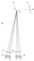
- FIG. 3 is a schematic diagram showing a semiconductor laser device 90 including the semiconductor laser element according to the first embodiment.
- the semiconductor laser device 90 is an external resonator type semiconductor laser device that combines wavelengths.
- a semiconductor laser device 90 includes semiconductor laser elements 101 and 102 , optical lenses 91 and 92 , a diffraction grating 95 and a partially reflecting mirror 97 .
- the semiconductor laser elements 101 and 102 are elements having the same structure and the same function as the semiconductor laser element 100 according to the first embodiment.
- the semiconductor laser elements 101 and 102 are laser array elements having a plurality of light emitting points. That is, the semiconductor laser elements 101 and 102 are used as small laser light sources that emit a plurality of laser beams. Therefore, the semiconductor laser device 90 can be, for example, a small semiconductor laser device on which the semiconductor laser elements 101 and 102 are mounted.
- Each of the semiconductor laser elements 101 and 102 has N light emitting points E11 to E1N (N is an integer equal to or greater than 2) and N light emitting points E21 to E2N.
- a plurality of laser beams are emitted from the light emitting points E11 to E1N.
- a plurality of laser beams are emitted from the light emitting points E21 to E2N.
- the wavelength of the laser light emitted from each light emitting point is determined according to the wavelength selection action by the external resonator including the diffraction grating 95 . Therefore, a plurality of laser beams having different wavelengths ⁇ 11 to ⁇ 1N are emitted from the light emitting points E11 to E1N as external resonance laser beams.
- a plurality of laser beams of ⁇ 2N are emitted as external resonance laser beams.
- the semiconductor laser elements 101 and 102 are arranged so that a plurality of laser beams propagate within the same plane.
- the optical lenses 91 and 92 are optical elements that condense a plurality of laser beams emitted from the semiconductor laser elements 101 and 102 onto the diffraction grating 95 .
- the optical lenses 91 and 92 may have a function of collimating the laser light.
- the semiconductor laser device 90 may include a collimating lens for collimating each laser beam.
- the diffraction grating 95 is a wavelength dispersive element that multiplexes a plurality of laser beams having different wavelengths, and is specifically a transmissive diffraction grating.
- a plurality of laser beams with different propagation directions can be transmitted on substantially the same optical axis. Can be synthesized.
- the diffraction grating 95 may be an element other than a transmissive diffraction grating, such as a prism or a reflective diffraction grating.
- the partially reflecting mirror 97 forms an external resonator with the non-emitting end faces of the semiconductor laser elements 101 and 102 .
- the partially reflecting mirror 97 functions as an output coupler that transmits (that is, emits) a portion of the laser light.
- the reflectance and transmittance of the partially reflecting mirror 97 are appropriately set according to the gains of the semiconductor laser elements 101 and 102 and the like.
- the semiconductor laser elements 101 and 102 each emit N laser beams when current is supplied.
- the N laser beams emitted from the semiconductor laser element 101 are condensed at a condensing point on the diffraction grating 95 by the optical lens 91 . Also, the N laser beams emitted from the semiconductor laser element 102 are condensed at a condensing point on the diffraction grating 95 by the optical lens 92 . Note that the laser light from the semiconductor laser element 101 and the laser light from the semiconductor laser element 102 are condensed at the same condensing point.
- the 2N laser beams are diffracted by the diffraction grating 95 and propagate along substantially the same optical axis toward the partially reflecting mirror 97 .
- a part of the laser light incident on the partial reflection mirror 97 is reflected by the partial reflection mirror 97, returns to the semiconductor laser element 101 or 102 via the diffraction grating 95 and the optical lens 91 or 92, and is reflected by each element. It is reflected by the output side end surface 50R. In this manner, an external resonator is formed between the non-emitting end face 50R of the semiconductor laser elements 101 and 102 and the partially reflecting mirror 97.
- the semiconductor laser elements 101 and 102 are arranged together with the optical lenses 91 and 92, the diffraction grating 95 and the partially reflecting mirror 97 to form an external resonator.
- the other portion of the laser light directed from the diffraction grating 95 toward the partially reflecting mirror 97 is transmitted through the partially reflecting mirror 97 and becomes the output light of the semiconductor laser device 90 .
- the output light is output as high-output laser light to the outside of the semiconductor laser device 90 via, for example, an optical fiber arranged on the optical axis of the output light.
- the wavelength synthesizing method used in the semiconductor laser device 90 of FIG. 3 and a spatial synthesizing method for spatially synthesizing laser beams.
- the wavelength combining method of condensing light of different wavelengths on the same optical axis is more advantageous than the spatial combining method.
- the optical path lengths from the emission side facet 50F to the diffraction grating 95 and the incident angles with respect to the diffraction grating 95 of the laser beams with wavelengths ⁇ 11 to ⁇ 1N emitted from the semiconductor laser element 101 are different from each other.
- the optical path lengths from the emission side facet 50F to the diffraction grating 95 and the incident angles with respect to the diffraction grating 95 of the laser beams with wavelengths ⁇ 21 to ⁇ 2N emitted from the semiconductor laser element 102 are different from each other. Therefore, the laser beams of different wavelengths ⁇ 11 to ⁇ 1N and ⁇ 21 to ⁇ 2N are diffracted by the diffraction grating 95, thereby changing the wavelengths of the laser beams.
- the semiconductor laser device 90 includes two semiconductor laser elements 101 and 102 in this embodiment, the semiconductor laser device 90 may include three or more semiconductor laser elements. As the number of semiconductor laser elements included in the semiconductor laser device 90 increases, the optical output value of the semiconductor laser device 90 can be increased.
- a plurality of semiconductor laser devices 90 that combine wavelengths may be used, and the output light from the semiconductor laser devices 90 may be combined by a spatial combining method to further increase the optical output.
- the semiconductor laser device 100 includes the semiconductor laminate 50 that emits laser light, the emission-side protective layer 1F disposed on the emission-side facet 50F of the semiconductor laminate 50, and the semiconductor laminate. and a non-emission-side protective layer 1R disposed on the end face (non-emission-side end face 50R) opposite to the emission-side end face 50F of the body 50 and reflecting the laser light.
- the output-side protective layer 1F has a control layer 22 that suppresses the reflectance on the output side with respect to the wavelength of the laser light to a predetermined value or less, and the control layer 22 suppresses distortion due to thermal expansion of the control layer 22. It has a strain relief layer 30 .
- the reflectance on the output side of the semiconductor laminate 50 can be maintained at a predetermined value or less.
- the thermal expansion of the output-side protective layer 1F can be suppressed, and the tensile stress generated at the interface between the output-side end surface 50F of the semiconductor laminate 50 and the output-side protective layer 1F can be reduced, deterioration of the output-side end surface 50F and deterioration of the output-side protective layer 1F can be prevented. Peeling of the protective layer 1F can be suppressed.
- the semiconductor laminate 50 has a plurality of light emitting points located on the emitting side facet 50F and emitting a plurality of laser beams. Moreover, the reflectance on the output side is less than or equal to a predetermined value with respect to the wavelength of the laser light.
- the semiconductor laser device 100 can emit a plurality of laser beams and can output high-quality laser beams. Further, by mounting the above-described semiconductor laser device 100 in an external resonator type semiconductor laser device 90 that performs wavelength synthesis, a semiconductor laser device that outputs high-quality laser light can be realized.
- the semiconductor laser device 100 when used in an external cavity type semiconductor laser device 90 that performs wavelength synthesis, an external cavity is formed between the partially reflecting mirror 97 and the non-emitting facet of the semiconductor laser device. That is, a plurality of laser beams having different wavelengths are transmitted through the emission-side protective layer 1F.
- the reflectance on the emission side with respect to the wavelength of each laser beam can be reduced. can be suppressed to a predetermined value or less. Therefore, the configuration and manufacturing process of the semiconductor laser device 90 can be simplified. That is, manufacturing errors of the semiconductor laser device can be reduced, the manufacturing process can be stabilized, and cost reduction can be realized.
- the reflectance on the emission side with respect to the wavelength of the laser light emitted from the semiconductor laser element 100 is suppressed to 1.0% or less.
- the strain relaxation layer 30 is arranged at an intermediate position in the control layer 22 in the traveling direction of the laser light.
- the exit-side protective layer 1F further has a barrier layer 21 arranged between the exit-side end face 50F and the control layer 22.
- the semiconductor laser element 100 is a gallium nitride-based semiconductor laser element
- diffusion of oxygen from the outside of the output-side protective layer 1F to the semiconductor laminate 50 easily deteriorates the output-side protective layer 1F and the output-side facet 50F.
- the barrier layer 21 on the output-side protective layer 1F
- diffusion of oxygen from the outside of the output-side protective layer 1F to the semiconductor stacked body 50 can be reduced. Therefore, it is possible to suppress the deterioration of the output-side protective layer 1F and the exit-side end surface 50F. Therefore, the reliability of the output of the semiconductor laser device 100 can be improved, and the operation period can be lengthened.
- the emission-side protective layer 1F tends to be thick.
- the thicker the output-side protective layer 1F the greater the tensile stress generated at the interface between the output-side protective layer 1F and the output-side end surface 50F when the output-side protective layer 1F thermally expands. Therefore, the emission-side end surface 50F is likely to deteriorate.
- the exit-side protective layer 1F of this embodiment has a barrier layer 21 and is relatively thick as a whole. However, the exit-side protective layer 1F has the control layer 22 including the strain relaxation layer 30. FIG. Therefore, in a device that emits high-energy laser light, such as a gallium nitride-based semiconductor laser device, it is possible to output high-energy laser light and improve the quality of the laser light while keeping the reflectance on the emission side low. can.
- the protection performance of the exit-side facet 50F can be enhanced.
- the thickness of the strain relaxation layer 30 is 2 nm or less.
- strain relaxation layer 30 Since the strain relaxation layer 30 is thin, even if the control layer 22 has the strain relaxation layer 30, compared with the emission side protective layer without the strain relaxation layer 30, the emission side of the output side for a plurality of wavelengths of laser light is reduced. Reflectance values and wavelength characteristics are unchanged.
- the strain relaxation layer 30 has the smallest coefficient of thermal expansion among the layers included in the output-side protective layer 1F.
- the strain relaxation layer 30 is made of SiO 2 .
- SiO 2 has a particularly small coefficient of thermal expansion (approximately 0.5), so deterioration of the emission-side facet 50F can be further suppressed.
- SiO 2 has a low light absorption in the wavelength band of the laser light emitted from the gallium nitride based semiconductor laser device. Therefore, absorption of laser light by the strain relaxation layer 30 can be suppressed.
- FIG. 4 is a schematic cross-sectional view showing a semiconductor laser device 200 according to the second embodiment.
- FIG. 4 shows a cross section of the semiconductor laser element 200 along a plane along the lamination direction of each layer of the semiconductor layered body 50 provided in the semiconductor laser element 200 and the emission direction of the laser light.
- the semiconductor laser element 200 is a semiconductor light emitting element that emits a plurality of laser beams.
- the semiconductor laser device 200 is a gallium nitride based semiconductor laser device.
- the semiconductor laser element 200 includes a semiconductor laminate 50, an emitting side protective layer 2F, and a non-emitting side protective layer 1R.
- the semiconductor laser device 200 differs from the semiconductor laser device 100 according to the first embodiment only in the structure and function of the emission-side protective layer 2F, and is otherwise the same in structure and function.
- the exit-side protective layer 2 ⁇ /b>F has a barrier layer 21 and a control layer 22 .
- the barrier layer 21 of the first embodiment has a single-layer structure
- the barrier layer 21 of this embodiment has a two-layer structure composed of the first layer 31 and the second layer 32 .
- the first layer 31 is in contact with the emission-side end surface 50F of the semiconductor laminate 50.
- the first layer 31 is a dielectric layer, specifically an oxynitride layer or a nitride layer.
- the first layer 31 is the same material as the barrier layer 21 of the first embodiment.
- the first layer 31 is a layer made of AlO 1-x N x (0 ⁇ x ⁇ 1), for example.
- the thickness of the first layer 31 is, for example, about 20 nm.
- the first layer 31 may be an oxynitride layer such as a SiO 1-x N x (0 ⁇ x ⁇ 1) layer, or a nitride layer such as an AlN layer or a SiN layer.
- the second layer 32 is a layer arranged in contact with the output side surface of the first layer 31 .
- the second layer 32 has a function of enhancing the protection performance of the emission-side end surface 50F.
- the second layer 32 is a dielectric layer, specifically an oxynitride layer, a nitride layer, or an oxide layer.
- the second layer 32 is a layer made of Al 2 O 3 , for example.
- the thickness of the second layer 32 is, for example, about 10 nm.
- the second layer 32 is a SiO 1-x N x (0 ⁇ x ⁇ 1) layer, an oxynitride layer such as an AlO 1-x N x (0 ⁇ x ⁇ 1) layer, a SiN layer, or , a nitride layer such as an AlN layer, or an oxide layer such as a SiO2 layer.
- the control layer 22 is farther from the emission-side end surface 50F than the barrier layer 21 and is arranged in contact with the emission side surface of the barrier layer 21 .
- the control layer 22 has an inner layer 33 , an intermediate layer 34 and an outer layer 35 . These layers are all dielectric layers, and are arranged in order of the inner layer 33 , the intermediate layer 34 and the outer layer 35 from the side closer to the barrier layer 21 .
- control layer 22 Since the control layer 22 has three types of layers, the inner layer 33, the intermediate layer 34, and the outer layer 35, the reflectance on the output side is 1% or less for a wider range of wavelengths than in the first embodiment. can be suppressed to
- the inner layer 33 is a layer made of Al2O3 , for example.
- the thickness of the inner layer 33 is, for example, about 100 nm.
- the outer layer 35 is, for example, a layer made of SiO2 .
- the thickness of the outer layer 35 is, for example, about 100 nm.
- the intermediate layer 34 has a main intermediate layer 34 a that contributes to adjusting the reflectance, and a strain relaxation layer 30 that relaxes the strain of the control layer 22 as a whole.
- the materials of the main intermediate layer 34a and the strain relaxation layer 30 are different.
- the main intermediate layer 34a is, for example, a layer made of ZrO2 .
- the main intermediate layer 34a may be a layer formed of a material having a higher refractive index with respect to laser light than either of the inner layer 33 and the outer layer 35 .
- the main intermediate layer 34a is, for example, an AlO 1-x N x (0 ⁇ x ⁇ 1) layer, an oxynitride layer such as a SiO 1-x N x (0 ⁇ x ⁇ 1) layer, a SiN layer, or , a nitride layer such as an AlN layer, an oxide layer such as a TiO 2 layer, a Nb 2 O 5 layer, a Ta 2 O 5 layer, or an HfO 2 layer.
- the inner layer 33 may be a layer other than the Al 2 O 3 layer. If the inner layer 33 is a layer other than an Al2O3 layer, the main intermediate layer 34a may be an Al2O3 layer.
- the inner layer 33 and the outer layer 35 may be layers formed of a material having a lower refractive index for laser light than the main intermediate layer 34a.
- the inner layer 33 is, for example, an AlO 1-x N x (0 ⁇ x ⁇ 1) layer, an oxynitride layer such as a SiO 1-x N x (0 ⁇ x ⁇ 1) layer, or an SiO 2 layer. It may be an oxide layer such as
- the outer layer 35 is, for example, an AlO 1-x N x (0 ⁇ x ⁇ 1) layer, an oxynitride layer such as a SiO 1-x N x (0 ⁇ x ⁇ 1) layer, or an Al It may also be an oxide layer such as a 2 O 3 layer.
- the strain relaxation layer 30 is arranged so as to be inserted in an intermediate position of the intermediate layer 34 in the traveling direction of the laser light. That is, the strain relaxation layer 30 is sandwiched between two main intermediate layers 34a.
- the two main intermediate layers 34a may be made of the same material, or may be made of different materials.
- the strain relaxation layer 30 is made of SiO 2 and has a thickness of about 2 nm, as in the first embodiment. On the other hand, the total thickness of the main intermediate layers 34a on both sides of the strain relaxation layer 30 is, for example, about 50 nm.
- the strain relaxation layer 30 may be made of a material having a smaller thermal expansion coefficient than at least the main intermediate layer 34a. More desirably, the strain relaxation layer 30 is made of a material having the smallest coefficient of thermal expansion among the layers included in the output-side protective layer 2F. Further, the strain relaxation layer 30 may be an AlO 1-x N x (0 ⁇ x ⁇ 1) layer or a SiO 1-x N layer depending on the materials of the layers other than the strain relaxation layer 30 in the output-side protective layer 2F.
- an oxynitride layer such as an x (0 ⁇ x ⁇ 1) layer, a nitride layer such as an AlN layer or a SiN layer, or an Al 2 O 3 layer, a Ta 2 O 5 layer or a HfO 2 layer It may be an oxide layer.
- control layer 22 has the strain relaxation layer 30, so that the same effect as in the first embodiment can be obtained.
- control layer 22 since the control layer 22 has the strain relaxation layer 30 made of a material with a small thermal expansion coefficient, the tensile stress generated at the interface between the output-side protective layer 2F and the output-side end surface 50F can be reduced. Therefore, the reflectance of the semiconductor laser element 200 on the emission side can be reduced, and the laser quality can be improved.
- the strain relaxation layer 30 is arranged at an intermediate position in the intermediate layer 34 in the traveling direction of the laser light. Therefore, it is possible to further suppress distortion due to thermal expansion of the output-side protective layer 2F as a whole, and to further suppress deterioration of the output-side protective layer 2F.
- the thickness of the strain relaxation layer 30 should be 2 nm or less.
- the semiconductor laser device 200 does not have the strain relaxation layer 30, and the output side is protected in the points other than not having the strain relaxation layer 30.
- the wavelength characteristics with respect to laser light are equivalent.
- the control layer 22 of this embodiment has an inner layer 33, a main intermediate layer 34a, and an outer layer 35, and an output-side protective layer without the strain relaxation layer 30 is disposed on the output-side end surface 50F.
- the inner layer 33, the main intermediate layer 34a, and the outer layer 35 are configured so that the reflectance on the output side is suppressed to 1.0% or less for each oscillation wavelength of the laser light. . Therefore, the reflectance on the output side of the laser light can be suppressed to 1.0% or less.
- the reflectance on the output side can be suppressed to 1.0% or less for a wider range of wavelengths.
- the semiconductor laser device 200 of the second embodiment has the output side facet 50F, so that the reflectance on the output side is 1% for wavelengths included in a wavelength range with a wavelength width of 50 nm or more. can be reduced to the following.
- the reflectance on the output side can be appropriately changed.
- the strain relaxation layer 30 has substantially the same reflectance and wavelength characteristics on the exit side regardless of the position of the strain relaxation layer 30 on the control layer 22 . That is, the strain relief layer 30 may be placed anywhere in the control layer 22 , for example, the inner layer 33 or the outer layer 35 may have the strain relief layer 30 .
- the barrier layer 21 of the second embodiment has a two-layer structure, it may have a layer structure composed of three or more layers.
- at least the layer in contact with the emission-side facet 50F should be a layer corresponding to the first layer 31, that is, an oxynitride layer or a nitride layer.
- the two or more layers other than the layer in contact with the output-side facet 50F are necessarily AlO 1-x N x (0 ⁇ x ⁇ 1) layers or SiO 1-x N x (0 ⁇ x ⁇ 1) layers. It may not be an oxynitride layer, or a nitride layer such as an AlN layer or a SiN layer, but may be an oxide layer such as an Al2O3 layer or an SiO2 layer.
- the first layer 31 may have a multi-layer structure composed of at least one layer of an oxynitride layer and a nitride layer.
- the semiconductor laser device 200 is a gallium nitride based semiconductor laser device, and the barrier layer 21 includes the first layer 31 which is an oxynitride layer or a nitride layer. .
- the first layer 31 on the output-side facet 50F By arranging the first layer 31 on the output-side facet 50F, diffusion of oxygen from the outside of the output-side protective layer 2F to the semiconductor laminate 50 can be reduced. Therefore, the deterioration of the emission-side protective layer 2F can be suppressed, the reliability of the output of the semiconductor laser device 100 can be improved, and the operation period can be lengthened.
- the layer (first layer 31) in contact with the emission-side facet 50F is an oxynitride layer or a nitride layer having the same crystallinity as the semiconductor stacked body 50. Therefore, it is possible to enhance the protective performance of the emission-side end surface 50F.
- the barrier layer 21 includes, in addition to the first layer 31, a second layer 32 which is an oxynitride layer, a nitride layer, or an oxide layer.
- the diffusion of oxygen from the outside of the emission-side protective layer 2F to the semiconductor laminate 50 can be further reduced.
- deterioration of the emission-side facet 50F can be further suppressed, so that the quality of the laser light from the semiconductor laser device 100 can be further improved, and the operating period can be extended.
- the control layer 22 has an inner layer 33 , an intermediate layer 34 and an outer layer 35 , the inner layer 33 , the intermediate layer 34 and the outer layer 35 having the inner layer 33 , the intermediate layer 34 and the outer layer 35 with respect to the barrier layer 21 .
- 34 and the outer layer 35 are arranged in this order.
- the intermediate layer 34 has the strain relief layer 30 , and the main intermediate layer 34 a of the intermediate layer 34 is made of a material different from that of the inner layer 33 and the outer layer 35 .
- the refractive index of the main intermediate layer 34a for laser light is greater than that of both the inner layer 33 and the outer layer 35 for laser light.
- the reflectance on the output side can be suppressed to 1% or less for a wider range of wavelengths than in the first embodiment.
- the inner layer 33 and the outer layer 35 are AlO 1-x N x (0 ⁇ x ⁇ 1), SiO 1-x N x (0 ⁇ x ⁇ 1), SiO 2 and Al 2 O 3 respectively. is formed by Thus, inner layer 33 and outer layer 35 with relatively low refractive indices are realized.
- the main intermediate layer 34a is made of AlO 1-x N x (0 ⁇ x ⁇ 1), SiO 1-x N x (0 ⁇ x ⁇ 1), AlN, SiN, Al 2 O 3 , ZrO 2 , TiO 2 , Nb 2 O 5 , Ta 2 O 5 or HfO 2 . Therefore, the main intermediate layer 34a having a relatively high refractive index is realized.
- the output-side protective layers 1F and 2F have at least one or more of an oxynitride layer, a nitride layer, or an oxide layer in addition to the strain relaxation layer 30. Even with such a structure, the reflectance on the output side can be suppressed to a predetermined value or less, and the laser quality can be improved.
- the non-emission side protective layer 1R may have any layer structure as long as the reflectance on the non-emission side can be secured at a certain value or higher. As long as the non-emission-side protective layer 1R has at least one layer of an oxynitride layer, a nitride layer, or an oxide layer, any layer structure may be used. And the effects of the second embodiment are not reduced.
- the semiconductor laser device 100 has a plurality of light emitting points, but even if it has a single light emitting point, the same effect can be obtained. That is, it is possible to suppress the reflectance on the output side with respect to the wavelength of the laser light emitted from the semiconductor laser device 100 to a predetermined value or less, thereby realizing improvements in laser quality and output.
- the semiconductor laser element does not have to be a gallium nitride semiconductor laser element.
- the semiconductor laser device may be an AlGaInP semiconductor laser device, a gallium arsenide semiconductor laser device, or an InP semiconductor laser device.
- the semiconductor laser element is an AlGaInP-based semiconductor laser element
- the wavelength of the emitted laser light is in the red wavelength band (band of 600 nm or more and 700 nm or less).
- the semiconductor laser device is a gallium arsenide-based semiconductor laser device
- the wavelength of the emitted laser light is in the infrared wavelength band (750 nm or more and 1100 nm or less).
- the semiconductor laser element is an InP-based semiconductor laser element, the wavelength of the emitted laser light is in the 1 ⁇ m band.
- the semiconductor laser device 100 does not necessarily have to have the barrier layer 21 .
- the semiconductor laser device is an AlGaInP semiconductor laser device, a gallium arsenide semiconductor laser device, or an InP semiconductor laser device
- the diffusion of oxygen from the outside of the emission-side protective layers 1F and 2F to the semiconductor laminate 50 causes Deterioration of the outgoing end face 50F is less likely to occur.
- first embodiment Both the semiconductor laser device having the strain relaxation layer 30 (hereinafter referred to as “first embodiment”) and the semiconductor laser device having no strain relaxation layer 30 (hereinafter referred to as “comparative example”) were tested.
- the catastrophic optical damage (COD) level of the element was examined.
- the following conditions (1) and (2) are common to the first embodiment and the comparative example.
- (1) When the wavelength of the laser light emitted from the semiconductor laser element is ⁇ , the total thickness of the protective layer on the output side is approximately ⁇ /2.
- the thickness of the control layer 22 is about 3 ⁇ /8 Specifically, a reliability test was performed on the semiconductor laser devices of the first example and the comparative example, and the COD level was evaluated based on the change in optical output value before and after the reliability test. As a reliability test, the inventor continuously output laser light from the semiconductor laser devices of Examples and Comparative Examples for a long time (here, 1000 hours). The measurement results of the light output values of both devices are shown in Table 2 below.
- the light output value of the semiconductor laser device of the comparative example decreased significantly after the reliability test. That is, the COD level was significantly lowered.
- the amount of decrease in the optical output value after the reliability test was smaller than that before the reliability test. That is, it can be said that the decrease in the COD level was suppressed.
- the semiconductor laser device 100 according to the first embodiment has a strain relief layer in which the control layer 22 is made of a material having a smaller thermal expansion coefficient than the material of the main control layer 22a. has 30. Therefore, similarly to the semiconductor laser device of the first embodiment, it can be said that the tensile stress generated at the interface between the emission-side protective layer 1F and the emission-side facet 50F can be reduced, and deterioration of the emission-side facet 50F can be suppressed. Therefore, it can be said that the reflectance on the emission side of the semiconductor laser device 100 can be reduced and the laser quality can be improved.
- the semiconductor laser device 200 according to the second embodiment has the strain relief layer 30 in which the intermediate layer 34 of the control layer 22 is made of a material having a smaller thermal expansion coefficient than the material of the main intermediate layer 34a. Therefore, it can be said that an effect similar to that of the first embodiment can be obtained. Therefore, it can be said that the reflectance on the emission side of the semiconductor laser device 200 can be reduced and the laser quality can be improved.
- This appropriate value is the thickness of the strain relaxation layer 30 required to obtain the same reflectance as that of the semiconductor laser device having the emission side protective layer that does not include the strain relaxation layer 30. That is.
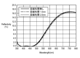
- FIG. 5 is a graph showing the reflectance on the emission side of the semiconductor laser device according to the second example.
- the solid line in FIG. 5 indicates the wavelength characteristics of the reflectance of a semiconductor laser device without a strain relaxation layer
- the one-dot chain line indicates the wavelength of the reflectance of a semiconductor laser device having a strain relaxation layer 30 with a thickness of 1 nm.
- the dashed line indicates the wavelength characteristics of the reflectance of the semiconductor laser device having the strain relaxation layer 30 with a thickness of 2 nm.
- These semiconductor laser devices according to the second example have control layers according to the second embodiment, that is, control layers composed of an inner layer, an intermediate layer, and an outer layer. Also, the intermediate layer of the semiconductor laser device having the strain relaxation layer 30 has a SiO 2 layer as the strain relaxation layer 30 .
- the thickness of the strain relaxation layer was 2.0 nm or less, the reflectance wavelength characteristics equivalent to those of the semiconductor laser device without the strain relaxation layer 30 were exhibited. Moreover, when the thickness of the strain relaxation layer is 2.0 nm or less, a reflectance of 1.0% or less can be achieved in the 450 nm band including the oscillation wavelength of the laser light.
- the thickness of the strain relaxation layer 30 is set to 2.0 nm or less, wavelength characteristics of reflectance equivalent to those of a semiconductor laser device without the strain relaxation layer 30 can be obtained. Further, when the output-side protective layer without the strain relaxation layer 30 suppresses the reflectance on the output side to 1.0% or less at the oscillation wavelength of the laser light, the strain-relaxing layer It can be said that even with the addition of layer 30, the reflectance on the output side is maintained below 1.0%.
- the semiconductor laser device 100 has the strain relaxation layer 30 with a thickness of 2.0 nm or less. It can be said that the wavelength characteristics of the reflectance on the output side of the device 100 are not changed.
- the main control layer is arranged such that the reflectance on the output side is suppressed to 1.0% or less with respect to the oscillation wavelength of the laser light. 22a, even if the strain relaxation layer 30 is added to the output-side protective layer 1F, it can be said that the output-side reflectance can be maintained at 1.0% or less with respect to the oscillation wavelength of the laser light.
- the semiconductor laser device 200 according to the second embodiment has the strain relaxation layer 30 with a thickness of 2.0 nm or less. It can be said that the wavelength characteristics of the reflectance on the emission side of the semiconductor laser element 200 defined by the above are not changed.
- the inner side is arranged so that the reflectance on the output side is suppressed to 1.0% or less with respect to the oscillation wavelength of the laser light.
- the semiconductor laser device 200 of the second embodiment and the semiconductor laser device of the second example are similar in structure. That is, in the semiconductor laser device 200 according to the second embodiment, the control layer 22 has the inner layer 33, the intermediate layer 34, and the outer layer 35, like the semiconductor laser device according to the second embodiment. Therefore, according to the semiconductor laser device 200 according to the second embodiment, it can be said that the wavelength characteristics of the reflectance on the output side are close to the wavelength characteristics of FIG.
- the semiconductor laser device 200 of the second embodiment has the emission-side protective layer 2F, so that the reflectance on the emission side can be suppressed to 1% or less in a wavelength range having a wavelength width of 50 nm or more. guessed.
- the reflectance on the output side is 1% or less in the wavelength range where the center wavelength is about 420 nm and the wavelength width is about 130 nm. is assumed to be reduced to
- the reflectance on the exit side can be suppressed to 1.0% or less for a wider range of wavelengths than in the first embodiment.
- the inventor changed the position of the strain relaxation layer 30 in the control layer 22 and examined the wavelength characteristics of the reflectance on the output side. had the same reflectance. That is, when layers other than the strain relaxation layer 30 included in the output side protective layers 1F and 2F are configured so that the reflectance on the output side is 1% or less with respect to the oscillation wavelength of the laser light, the strain relief It can be said that regardless of the position of the layer 30 in the control layer 22, the reflectance on the output side is suppressed to 1% or less with respect to the oscillation wavelength of the laser light. For example, in the second embodiment, even if the inner layer 33 or the outer layer 35 has the strain relaxation layer 30, the reflectance on the output side and its wavelength characteristics are substantially the same.
- the present disclosure it is possible to provide a semiconductor laser device capable of reducing the reflectance on the laser light emitting end face side and improving the laser quality.
- the present disclosure can be suitably applied to a semiconductor laser device in which a protective layer is arranged on the laser light emitting facet side.
Abstract
This semiconductor laser element comprises: a semiconductor laminate that emits a laser beam; an emitting-side protective layer disposed on a laser beam emitting-side end face of the semiconductor laminate; and a non-emitting-side protective layer that is disposed on an end face of the semiconductor laminate on the side opposite from the laser beam emitting-side end face and that reflects the laser beam, wherein the emitting-side protective layer has a control layer that suppresses emitting-side reflectance with respect to the wavelength of the laser beam to a prescribed value or lower, and the control layer has a strain relief layer inhibiting strain associated with the thermal expansion of the control layer.
Description
本開示は、半導体レーザ素子に関する。
The present disclosure relates to a semiconductor laser device.
従来、レーザ装置を用いたレーザ加工技術が実用化されている。レーザ加工技術の用途を拡大するためには、レーザ光の高出力化及び高品質化が求められる。一般に、レーザ光の高品質化には、レーザ光の狭ビーム化が必要である。
Conventionally, laser processing technology using laser equipment has been put into practical use. In order to expand the use of laser processing technology, higher power and higher quality of laser light are required. In general, to improve the quality of laser light, it is necessary to narrow the beam of laser light.
レーザ装置の一例として、半導体レーザ素子から離隔して配置される回折格子等の光学部品によりレーザ光の共振状態を形成する外部共振器を備える外部共振型レーザ装置がある。外部共振型レーザ装置において、半導体レーザ素子から出射される複数のレーザ光を合成する合成光学系を外部共振器内に構築することで、高出力かつ高品質のレーザ光を出射することができる。
As an example of a laser device, there is an external resonance type laser device that includes an external resonator that forms a resonant state of laser light with an optical component such as a diffraction grating that is spaced apart from a semiconductor laser element. In an external cavity laser device, a high-output and high-quality laser light can be emitted by constructing a synthesizing optical system for synthesizing a plurality of laser lights emitted from a semiconductor laser element in the external cavity.
複数のレーザ光の合成手法としては、空間合成法と波長合成法とがある。空間合成法は、同じ光軸上には集光せずに、複数のレーザ光を空間的に合成する手法である。一方、波長合成法は、互いに異なる波長を有する複数のレーザ光を同じ光軸上に集光する手法である。複数のレーザ光を合成して狭ビーム化を実現するためには、複数の光軸が互いに異なる空間合成法よりも波長合成法の方が好ましい。
There are spatial synthesis method and wavelength synthesis method as methods for synthesizing multiple laser beams. The spatial synthesis method is a method of spatially synthesizing a plurality of laser beams without focusing them on the same optical axis. On the other hand, the wavelength combining method is a method of condensing a plurality of laser beams having different wavelengths on the same optical axis. In order to achieve a narrow beam by synthesizing a plurality of laser beams, a wavelength synthesis method is preferable to a spatial synthesis method in which a plurality of optical axes are different from each other.
また、波長合成法を適用する場合、例えば、半導体レーザ素子として、複数の発光点を有する半導体レーザ素子(いわゆる、レーザアレイ素子)が採用される。
Also, when applying the wavelength combining method, for example, a semiconductor laser element having a plurality of light emitting points (so-called laser array element) is adopted as the semiconductor laser element.
ところで、外部共振型レーザ装置においては、レーザアレイ素子内での内部共振を抑制するために、レーザアレイ素子のレーザ光出射側端面の反射率を極力低減する必要がある。この出射側端面側の反射率は、例えば、1%以下であることが求められる。
By the way, in an external resonance type laser device, it is necessary to reduce the reflectance of the laser light emitting side facet of the laser array element as much as possible in order to suppress internal resonance within the laser array element. For example, the reflectance of the exit facet is required to be 1% or less.
例えば、特許文献1には、多波長半導体レーザ素子のレーザ光出射側端面に、複数の誘電体層で構成された出射側保護層を設けることで、出射側端面の反射率を低減することが開示されている。図1は、特許文献1の多波長半導体レーザ素子の平面構成を示す模式図である。
For example, in Patent Document 1, it is possible to reduce the reflectance of the emission side end face by providing an emission side protective layer composed of a plurality of dielectric layers on the laser light emission side facet of a multi-wavelength semiconductor laser element. disclosed. FIG. 1 is a schematic diagram showing a planar configuration of the multi-wavelength semiconductor laser device of Patent Document 1. As shown in FIG.
特許文献1に開示されている多波長半導体レーザ素子は、650nm帯のレーザ光を出射する第1発光部11と、780nm帯のレーザ光を出射する第2発光部12とを有している。また、多波長半導体レーザ素子は、レーザ光出射側端面に、複数の誘電体層14A、14B、14Cで構成された出射側保護層14を有している。出射側保護層14は、650nm帯と780nm帯とを含む波長範囲のレーザ光に対する出射側端面の反射率を低減する。
The multi-wavelength semiconductor laser device disclosed in Patent Document 1 has a first light emitting section 11 that emits laser light in the 650 nm band and a second light emitting section 12 that emits laser light in the 780 nm band. The multi-wavelength semiconductor laser element also has an emission-side protective layer 14 composed of a plurality of dielectric layers 14A, 14B, and 14C on the laser light emission-side facet. The emission-side protective layer 14 reduces the reflectance of the emission-side facet for laser light in a wavelength range including the 650 nm band and the 780 nm band.
本開示の一態様に係る半導体レーザ素子は、
レーザ光を出射する半導体積層体と、
前記半導体積層体のレーザ光出射側端面に配置される出射側保護層と、
前記半導体積層体の前記レーザ光出射側端面とは反対側の端面に配置され、前記レーザ光を反射させる非出射側保護層と、
を備え、
前記出射側保護層は、前記レーザ光の波長に対する出射側の反射率を所定値以下に抑制する制御層を有しており、
前記制御層は、前記制御層の熱膨張に伴う歪みを抑制する歪緩和層を有する。 A semiconductor laser device according to an aspect of the present disclosure includes
a semiconductor laminate that emits laser light;
an output-side protective layer disposed on the laser light output-side facet of the semiconductor laminate;
a non-emission-side protective layer arranged on an end face opposite to the laser light emission-side end face of the semiconductor laminate and reflecting the laser light;
with
The emission-side protective layer has a control layer that suppresses the reflectance on the emission side with respect to the wavelength of the laser beam to a predetermined value or less,
The control layer has a strain relief layer that suppresses strain due to thermal expansion of the control layer.
半導体レーザ素子の出射側保護層の構造は、レーザ光の信頼性を確保するために、例えば、構成する層の種類や層の厚さが増加されるなど、適宜調整される。また、出射側保護層の構造は、所望のレーザ特性を実現するために、出射側保護層内部での反射を含む出射側端面側の全体の反射率が抑制されように、適宜調整される。
The structure of the emission-side protective layer of the semiconductor laser element is appropriately adjusted, for example, by increasing the types and thicknesses of the constituent layers, in order to ensure the reliability of the laser light. In addition, the structure of the output-side protective layer is appropriately adjusted so as to suppress the overall reflectance on the output-side facet including reflection inside the output-side protective layer in order to achieve desired laser characteristics.
しかしながら、出射側保護層に熱膨張係数が高い層が含まれる場合、出射側保護層の熱膨張に起因する内部応力により、出射側保護層の剥がれや多波長半導体レーザ素子のレーザ光出射側端面の劣化が生じ、ひいては、レーザ品質の悪化を招く虞がある。加えて、出射側保護層が厚くなるほど、内部応力によりレーザ品質が悪化しやすくなる。
However, if the output-side protective layer includes a layer with a high coefficient of thermal expansion, the internal stress caused by the thermal expansion of the output-side protective layer may cause peeling of the output-side protective layer or damage to the laser light output-side facet of the multi-wavelength semiconductor laser device. , which may lead to deterioration of laser quality. In addition, the thicker the exit-side protective layer is, the more easily the laser quality deteriorates due to internal stress.
本開示は、レーザ光出射側端面側の反射率を低減できるとともに、レーザ品質を向上させることのできる半導体レーザ素子を提供することを目的としている。
An object of the present disclosure is to provide a semiconductor laser element capable of reducing the reflectance on the laser light emitting end face side and improving the laser quality.
以下、本開示の各実施形態及び変形例について、図面を参照しながら説明する。なお、以下に説明する各実施形態及び変形例は、いずれも本開示の一具体例を示すものである。従って、以下の各実施形態及び変形例で示される、数値、形状、材料、構成要素、及び、構成要素の配置位置や接続形態などは、一例であって本開示を限定する主旨では記載されていない。また、各図は模式的に示す図であり、必ずしも厳密に図示されたものではない。従って、各図において縮尺等は必ずしも一致していない。なお、各図において、実質的に同一の構成要素に対しては同一の符号を付しており、重複する説明は省略又は簡略化する。また、本明細書において、「上方」及び「下方」という用語は、絶対的な空間認識における上方向(鉛直上方)及び下方向(鉛直下方)を指すものではなく、後述する半導体積層体の積層構成における積層順を基に相対的な位置関係により規定される用語として用いる。また、「上方」及び「下方」という用語は、2つの構成要素が互いに間隔をあけて配置されて2つの構成要素の間に別の構成要素が存在する場合のみならず、2つの構成要素が互いに接する状態で配置される場合にも適用される。
Hereinafter, each embodiment and modifications of the present disclosure will be described with reference to the drawings. It should be noted that each of the embodiments and modifications described below is one specific example of the present disclosure. Therefore, the numerical values, shapes, materials, components, and arrangement positions and connection forms of the components shown in the following embodiments and modifications are examples and are not intended to limit the present disclosure. do not have. Also, each figure is a schematic diagram and is not necessarily strictly illustrated. Therefore, the scales and the like are not always the same in each drawing. In addition, in each figure, the same code|symbol is attached|subjected to the substantially same component, and the overlapping description is abbreviate|omitted or simplified. In this specification, the terms "upper" and "lower" do not refer to the upward direction (vertical upward) and the downward direction (vertical downward) in absolute spatial recognition, but to the stacking of semiconductor stacks described later. It is used as a term defined by a relative positional relationship based on the stacking order in the configuration. Also, the terms "above" and "below" are used not only when two components are spaced apart from each other and there is another component between the two components, but also when two components are spaced apart from each other. It also applies when they are arranged in contact with each other.
(第1実施形態)
以下、図2を参照しながら、第1実施形態に係る半導体レーザ素子100について説明する。図2は、第1実施形態に係る半導体レーザ素子100を示す模式的な断面図である。図2には、半導体積層体50(後述)の各層の積層方向、及び、レーザ光の出射方向に沿う平面による半導体レーザ素子100の断面が示されている。 (First embodiment)
Thesemiconductor laser device 100 according to the first embodiment will be described below with reference to FIG. FIG. 2 is a schematic cross-sectional view showing the semiconductor laser device 100 according to the first embodiment. FIG. 2 shows a cross-section of the semiconductor laser element 100 along a plane along the lamination direction of each layer of the semiconductor laminate 50 (described later) and the emission direction of the laser light.
以下、図2を参照しながら、第1実施形態に係る半導体レーザ素子100について説明する。図2は、第1実施形態に係る半導体レーザ素子100を示す模式的な断面図である。図2には、半導体積層体50(後述)の各層の積層方向、及び、レーザ光の出射方向に沿う平面による半導体レーザ素子100の断面が示されている。 (First embodiment)
The
[1-1.全体構成]
半導体レーザ素子100は、複数のレーザ光を出射する半導体発光素子、いわゆる、半導体レーザアレイである。本実施形態では、半導体レーザ素子100は、窒化ガリウム系半導体レーザ素子であり、390nm以上530nm以下程度の帯域の波長を有するレーザ光を出射する。 [1-1. overall structure]
Thesemiconductor laser device 100 is a semiconductor light emitting device that emits a plurality of laser beams, a so-called semiconductor laser array. In this embodiment, the semiconductor laser device 100 is a gallium nitride-based semiconductor laser device, and emits laser light having a wavelength in a band of about 390 nm to 530 nm.
半導体レーザ素子100は、複数のレーザ光を出射する半導体発光素子、いわゆる、半導体レーザアレイである。本実施形態では、半導体レーザ素子100は、窒化ガリウム系半導体レーザ素子であり、390nm以上530nm以下程度の帯域の波長を有するレーザ光を出射する。 [1-1. overall structure]
The
半導体レーザ素子100は、半導体積層体50と、出射側保護層1Fと、非出射側保護層1Rと、を備える。
The semiconductor laser element 100 includes a semiconductor laminate 50, an emitting-side protective layer 1F, and a non-emitting-side protective layer 1R.
[1-1-1.半導体積層体]
半導体積層体50は、複数の半導体層の積層体である。 [1-1-1. Semiconductor laminate]
The semiconductor laminate 50 is a laminate of a plurality of semiconductor layers.
半導体積層体50は、複数の半導体層の積層体である。 [1-1-1. Semiconductor laminate]
The semiconductor laminate 50 is a laminate of a plurality of semiconductor layers.
半導体積層体50は、基板51と、第1半導体層52と、活性層53と、第2半導体層54と、コンタクト層55とを有する。
The semiconductor laminate 50 has a substrate 51 , a first semiconductor layer 52 , an active layer 53 , a second semiconductor layer 54 and a contact layer 55 .
基板51は、半導体積層体50の基材となる板状部材である。本実施形態では、基板51は、GaN単結晶基板である。基板51の厚さは、例えば、約100μmである。基板51を形成する材料は、Al2O3(サファイア)、SiC、GaAs、または、InPなどの単結晶であってもよい。また、基板51の厚さは、例えば、50μm以上120μm以下であってもよい。
The substrate 51 is a plate-like member that serves as the base material of the semiconductor laminate 50 . In this embodiment, the substrate 51 is a GaN single crystal substrate. The thickness of the substrate 51 is, for example, approximately 100 μm. The material forming the substrate 51 may be single crystal such as Al 2 O 3 (sapphire), SiC, GaAs, or InP. Also, the thickness of the substrate 51 may be, for example, 50 μm or more and 120 μm or less.
第1半導体層52は、基板51の上方に形成される半導体層である。本実施形態では、第1半導体層52は、n型の半導体層であり、n型クラッド層を含む。
The first semiconductor layer 52 is a semiconductor layer formed above the substrate 51 . In this embodiment, the first semiconductor layer 52 is an n-type semiconductor layer and includes an n-type clad layer.
n型クラッド層は、n-Al0.2Ga0.8Nで形成されている層である。n型クラッド層の厚さは、例えば、約1μmである。なお、n型クラッド層は、例えば、n-AlxGa1-xN(0<x<1)で形成されていればよい。また、n型クラッド層の厚さは、例えば、0.5μm以上5μm以下であってもよい。
The n-type clad layer is a layer made of n-Al 0.2 Ga 0.8 N. The thickness of the n-type clad layer is, for example, about 1 μm. The n-type cladding layer may be made of, for example, n-Al x Ga 1-x N (0<x<1). Also, the thickness of the n-type cladding layer may be, for example, 0.5 μm or more and 5 μm or less.
また、n型クラッド層上にn型のAlxInyGa1-x―yN(0≦x+y≦1)ガイド層やアンドープのAlxInyGa1-x―yN(0≦x+y≦1)ガイド層が形成されていてもよい。
Further, an n-type Al x InyGa 1-x-yN (0≦x+y≦1) guide layer or an undoped Al x InyGa 1-x-yN (0≦x+y≦1) guide layer is formed on the n-type cladding layer. may be formed.
活性層53は、第1半導体層52の上方に形成される層である。活性層53は、発光層として機能する。本実施形態では、活性層53は、2層の井戸層を有している。具体的には、活性層53は、In0.18Ga0.82Nから形成されている井戸層、及び、GaNから形成されている障壁層とが交互に積層された量子井戸活性層である。ここで、井戸層の厚さは、例えば、約5nmであり、障壁層の厚さは、例えば、約10nmである。半導体レーザ素子100は、このような活性層53を備えることにより、例えば、波長が約450nmの青色レーザ光を出射できる。
The active layer 53 is a layer formed above the first semiconductor layer 52 . The active layer 53 functions as a light emitting layer. In this embodiment, the active layer 53 has two well layers. Specifically, the active layer 53 is a quantum well active layer in which well layers made of In 0.18 Ga 0.82 N and barrier layers made of GaN are alternately laminated. . Here, the thickness of the well layer is, for example, approximately 5 nm, and the thickness of the barrier layer is, for example, approximately 10 nm. By including such an active layer 53, the semiconductor laser device 100 can emit blue laser light with a wavelength of about 450 nm, for example.
活性層53は、InxGa1-xN(0<x<1)から形成されている井戸層と、AlxInyGa1-x―yN(0≦x+y≦1)から形成されている障壁層とが交互に積層された量子井戸活性層であればよい。
The active layer 53 is composed of a well layer made of InxGa1 -xN (0<x<1) and AlxInyGa1 -x-yN (0≤x+y≤1) . Quantum well active layers in which barrier layers are alternately laminated may be used.
なお、活性層53は、量子井戸活性層の上方及び下方の少なくとも一方にガイド層を有していてもよい。本実施形態では井戸層の数は2層であるが、1層以上4層以下であってもよい。また、波長範囲390nm以上530nm以下のうち、所望の波長の光が発光されるように井戸層のIn組成が適宜選択されてもよい。
Note that the active layer 53 may have a guide layer at least one of above and below the quantum well active layer. Although the number of well layers is two in this embodiment, it may be one to four. In addition, the In composition of the well layer may be appropriately selected so that light with a desired wavelength is emitted within the wavelength range of 390 nm or more and 530 nm or less.
第2半導体層54は、活性層53の上方に形成される半導体層である。本実施形態では、第2半導体層54は、p型の半導体層であり、p型クラッド層を含む。p型クラッド層は、p-Al0.2Ga0.8Nから形成された層と、GaNから形成された層とが交互に100層ずつ積層された超格子層である。p-Al0.2Ga0.8N層の厚さは、例えば、約3nmであり、GaN層の厚さは、例えば、約3nmである。
The second semiconductor layer 54 is a semiconductor layer formed above the active layer 53 . In this embodiment, the second semiconductor layer 54 is a p-type semiconductor layer and includes a p-type clad layer. The p-type cladding layer is a superlattice layer in which 100 layers of p-Al 0.2 Ga 0.8 N and 100 layers of GaN are alternately laminated. The thickness of the p-Al 0.2 Ga 0.8 N layer is, for example, approximately 3 nm, and the thickness of the GaN layer is, for example, approximately 3 nm.
p型クラッド層は、上述の超格子層ではなくとも、AlxGa1-xN(0<x<1)から形成された層であってもよい。なお、この層の厚さは、例えば、0.3μm以上1μm以下であってもよい。また、p型クラッド層は、AlxGa1-xN(0<x<1)からなるバルククラッド層であってもよい。
The p-type cladding layer may be a layer formed of Al x Ga 1-x N (0<x<1) instead of the superlattice layer described above. The thickness of this layer may be, for example, 0.3 μm or more and 1 μm or less. Also, the p-type clad layer may be a bulk clad layer made of Al x Ga 1-x N (0<x<1).
本実施形態では、p型クラッド層の材料として、AlGaNが用いられている。その理由は、AlGaNは、活性層53にレーザ光を閉じこめるために適した屈折率を有するからである。p型クラッド層の材料として、AlGaN以外の材料が用いられてもよい。例えば、p型クラッド層の材料として、ITOが用いられてもよい。また、p型クラッド層の材料として、出射されるレーザ光を透過する材料、例えば、In2O3、Ga2O3、SnO、InGaO3などの透明誘電体酸化物が用いられてもよい。
In this embodiment, AlGaN is used as the material of the p-type clad layer. The reason is that AlGaN has a refractive index suitable for confining laser light in the active layer 53 . Materials other than AlGaN may be used as the material of the p-type cladding layer. For example, ITO may be used as the material of the p-type clad layer. As the material of the p-type cladding layer, a material that transmits emitted laser light, such as a transparent dielectric oxide such as In 2 O 3 , Ga 2 O 3 , SnO, or InGaO 3 may be used.
また、第2半導体層54は、p型クラッド層の下方にp型のAlxInyGa1-x―yN(0≦x+y≦1)ガイド層やアンドープのAlxInyGa1-x-yN(0≦x+y≦1)ガイド層を複数有していてもよい。
The second semiconductor layer 54 includes a p-type Al x In y Ga 1-x-y N (0≦x+y≦1) guide layer and undoped Al x In y Ga 1-x under the p-type cladding layer. A plurality of -yN (0≤x+y≤1) guide layers may be provided.
コンタクト層55は、第2半導体層54の上方に形成される半導体層であり、第2電極57とオーミック接触する。本実施形態では、コンタクト層55は、p型の半導体層であり、p-GaNから形成されている。コンタクト層55の厚さは、例えば、約10nmである。
The contact layer 55 is a semiconductor layer formed above the second semiconductor layer 54 and is in ohmic contact with the second electrode 57 . In this embodiment, the contact layer 55 is a p-type semiconductor layer made of p-GaN. The thickness of the contact layer 55 is, for example, approximately 10 nm.
なお、コンタクト層55の材料はp-GaNに限定されない。また、コンタクト層55の厚さは、例えば、5nm以上200nm以下であってもよい。
The material of the contact layer 55 is not limited to p-GaN. Also, the thickness of the contact layer 55 may be, for example, 5 nm or more and 200 nm or less.
本実施形態では、第2半導体層54及びコンタクト層55に2以上のリッジ部が形成されている。各リッジ部に対応する活性層53の領域(つまり、各リッジ部の下方に位置する活性層53の領域)が発光点となり、複数の発光点からレーザ光が出射される。
In this embodiment, two or more ridges are formed in the second semiconductor layer 54 and contact layer 55 . A region of the active layer 53 corresponding to each ridge portion (that is, a region of the active layer 53 located below each ridge portion) serves as a light emitting point, and laser light is emitted from a plurality of light emitting points.
基板51の下方の主面(つまり、第1半導体層52などが配置されていない方の主面)には、電極として第1電極56が配置されている。
A first electrode 56 is arranged as an electrode on the lower main surface of the substrate 51 (that is, the main surface on which the first semiconductor layer 52 and the like are not arranged).
本実施形態では、第1電極56は、n側電極であり、基板51側から順にそれぞれTi層、Pt層及びAu層が積層された積層構造を有する。なお、第1電極56は、他の積層構造を有していてもよく、例えば、Ti層及びAu層が積層された積層構造を有していてもよい。
In this embodiment, the first electrode 56 is an n-side electrode and has a laminated structure in which a Ti layer, a Pt layer, and an Au layer are laminated in order from the substrate 51 side. Note that the first electrode 56 may have another laminated structure, for example, a laminated structure in which a Ti layer and an Au layer are laminated.
コンタクト層55上には、電極として第2電極57が配置されている。本実施形態では、第2電極57は、コンタクト層55とオーミック接触するp側電極と、p側電極上に配置されるパッド電極とを有する。
A second electrode 57 is arranged on the contact layer 55 as an electrode. In this embodiment, the second electrode 57 has a p-side electrode that makes ohmic contact with the contact layer 55 and a pad electrode that is arranged on the p-side electrode.
p側電極は、コンタクト層55側から順にそれぞれPd層及びPt層が積層された積層構造を有する。また、p側電極の構成はこれに限定されない。p側電極は、例えば、Cr層、Ti層、Ni層、Pd層、Pt層及びAu層の少なくとも一つを有する単層構造又は多層構造を有していてもよい。
The p-side electrode has a laminated structure in which a Pd layer and a Pt layer are laminated in order from the contact layer 55 side. Also, the configuration of the p-side electrode is not limited to this. The p-side electrode may have a single layer structure or a multilayer structure including at least one of a Cr layer, Ti layer, Ni layer, Pd layer, Pt layer and Au layer, for example.
また、p側電極は、透明酸化物電極として用いられるITO層であってもよいし、In2O3層、Ga2O3層、SnO層、または、InGaO3層であってもよい。
Also, the p-side electrode may be an ITO layer used as a transparent oxide electrode, an In 2 O 3 layer, a Ga 2 O 3 layer, an SnO layer, or an InGaO 3 layer.
パッド電極は、p側電極の上方に配置されたパッド状の電極である。本実施形態では、パッド電極は、p側電極側から順にそれぞれTi層及びAu層で形成された層が積層された積層構造を有しており、リッジ部及びその周辺に配置されている。
The pad electrode is a pad-shaped electrode arranged above the p-side electrode. In this embodiment, the pad electrode has a laminated structure in which layers formed of a Ti layer and an Au layer are laminated in order from the p-side electrode side, and are arranged on the ridge and its periphery.
パッド電極は、例えば、Au層のみで構成されていてもよいし、それぞれTi層、Pt層及びAu層が積層された積層構造や、それぞれNi層及びAu層が積層された積層構造を有していてもよい。また、パッド電極は、他の金属で形成された2以上の層が積層された積層構造を有していてもよい。
The pad electrode may be composed of, for example, only an Au layer, or may have a laminated structure in which a Ti layer, a Pt layer and an Au layer are laminated, or a laminated structure in which a Ni layer and an Au layer are laminated. may be Also, the pad electrode may have a laminated structure in which two or more layers made of another metal are laminated.
なお、図2には示されないが、半導体積層体50は、リッジ部の側壁などを覆うSiO2膜などの絶縁層などをさらに有してもよい。
Although not shown in FIG. 2, the semiconductor laminate 50 may further include an insulating layer such as an SiO 2 film covering the sidewalls of the ridge.
[1-1-2.非出射側保護層1R]
非出射側保護層1Rは、半導体積層体50のレーザ光非出射側端面50R(以下、「非出射側端面50R」と称す。)に配置される層である。非出射側保護層1Rは、非出射側端面50Rを保護し、レーザ光に対する半導体積層体50の非出射側の反射率を一定値(例えば、90%)以上に高める。ここで、「非出射側の反射率」とは、非出射側端面50Rと非出射側保護層1Rとを合わせて総合的に評価される反射率を意味する。 [1-1-2. Non-emission-sideprotective layer 1R]
The non-emission-sideprotective layer 1R is a layer arranged on the laser light non-emission-side facet 50R of the semiconductor laminate 50 (hereinafter referred to as "non-emission-side facet 50R"). The non-emission-side protective layer 1R protects the non-emission-side facet 50R and increases the reflectance of the non-emission side of the semiconductor laminate 50 with respect to laser light to a certain value (eg, 90%) or higher. Here, the “reflectance on the non-emission side” means the reflectance that is comprehensively evaluated by combining the non-emission-side end surface 50R and the non-emission-side protective layer 1R.
非出射側保護層1Rは、半導体積層体50のレーザ光非出射側端面50R(以下、「非出射側端面50R」と称す。)に配置される層である。非出射側保護層1Rは、非出射側端面50Rを保護し、レーザ光に対する半導体積層体50の非出射側の反射率を一定値(例えば、90%)以上に高める。ここで、「非出射側の反射率」とは、非出射側端面50Rと非出射側保護層1Rとを合わせて総合的に評価される反射率を意味する。 [1-1-2. Non-emission-side
The non-emission-side
本実施形態では、非出射側保護層1Rは、SiO2層及びAlO1-xNx(0<x<1)層の組が複数積層された多層構造を有する。SiO2層及びAlO1-xNx(0<x<1)層の厚さは、例えば、複数のレーザ光の平均波長をλaとして、SiO2層及びAlO1-xNx(0<x<1)層の屈折率をnとしたとき、それぞれλa/(4n)程度である。
In this embodiment, the non-emission-side protective layer 1R has a multi-layer structure in which a plurality of pairs of SiO 2 layers and AlO 1-x N x (0<x<1) layers are laminated. The thicknesses of the SiO 2 layer and the AlO 1-x N x (0<x<1) layer are, for example, SiO 2 layer and AlO 1-x N x (0<x<1), where λa is the average wavelength of a plurality of laser beams. <1) When the refractive index of each layer is n, it is approximately λa/(4n).
非出射側保護層1Rがこのような構造を有することで、レーザ光に対する非出射側の反射率が90%以上となる。これにより、スロープ効率が高く、かつ、閾値電流が低い半導体レーザ素子100を実現することができる。
With such a structure of the non-emission side protective layer 1R, the reflectance of the non-emission side with respect to the laser light becomes 90% or more. As a result, the semiconductor laser device 100 with high slope efficiency and low threshold current can be realized.
なお、非出射側保護層1Rは、非出射側の反射率が所望の値を得ることができれば、その積層構造は限定されない。例えば、非出射側保護層1Rは、SiO2層及びZrO2層の組、SiO2層及びTa2O5層の組、SiO2層及びAlN層の組、SiO2層及びTiO2層の組、SiO2層及びHfO2層の組、SiO2層及びNb2O5層の組、または、SiO2層及びAl2O3層の組などが複数積層された積層構造を有していてもよい。また、SiO2層及びAl2O3層の組を除く、上述の層の組のうち、低屈折率の層として、Al2O3層が用いられてもよい。
Note that the laminated structure of the non-emitting side protective layer 1R is not limited as long as a desired value of reflectance on the non-emitting side can be obtained. For example, the non-emission-side protective layer 1R includes a set of SiO 2 layer and ZrO 2 layer, a set of SiO 2 layer and Ta 2 O 5 layer, a set of SiO 2 layer and AlN layer, a set of SiO 2 layer and TiO 2 layer. , a set of SiO 2 layers and HfO 2 layers, a set of SiO 2 layers and Nb 2 O 5 layers, or a set of SiO 2 layers and Al 2 O 3 layers, etc. good. In addition, among the above-described layer sets, excluding the set of the SiO 2 layer and the Al 2 O 3 layer, the Al 2 O 3 layer may be used as the low refractive index layer.
また、非出射側保護層1Rは、酸窒化物層、または、窒化物層の少なくとも一方を含む単層構造または多層構造を有していてもよい。
Also, the non-emission-side protective layer 1R may have a single-layer structure or a multi-layer structure including at least one of an oxynitride layer and a nitride layer.
[1-1-3.出射側保護層1F]
出射側保護層1Fは、半導体積層体50のレーザ光出射側端面50F(以下、「出射側端面50F」と称す。)に配置される層である。出射側保護層1Fは、出射側端面50Fを保護するとともに、レーザ光に対する半導体積層体50の出射側の反射率を低減する。ここで、「出射側の反射率」とは、出射側端面50Fと出射側保護層1Fとを合わせて総合的に評価される反射率を意味する。 [1-1-3. Output-sideprotective layer 1F]
The emission-sideprotective layer 1F is a layer arranged on the laser light emission-side facet 50F of the semiconductor laminate 50 (hereinafter referred to as the "emission-side facet 50F"). The emission-side protective layer 1F protects the emission-side facet 50F and reduces the reflectance of the semiconductor laminate 50 on the emission side of the laser beam. Here, the “output-side reflectance” means the reflectance that is comprehensively evaluated by combining the output-side end face 50F and the output-side protective layer 1F.
出射側保護層1Fは、半導体積層体50のレーザ光出射側端面50F(以下、「出射側端面50F」と称す。)に配置される層である。出射側保護層1Fは、出射側端面50Fを保護するとともに、レーザ光に対する半導体積層体50の出射側の反射率を低減する。ここで、「出射側の反射率」とは、出射側端面50Fと出射側保護層1Fとを合わせて総合的に評価される反射率を意味する。 [1-1-3. Output-side
The emission-side
出射側保護層1Fは、バリア層21と、制御層22とを備えている。なお、以下の説明において、出射側の反射率を、単に「反射率」と呼ぶことがある。
The exit-side protective layer 1F includes a barrier layer 21 and a control layer 22. In the following description, the reflectance on the output side may be simply called "reflectance".
<バリア層>
バリア層21は、出射側端面50Fに接して配置されている。バリア層21は、半導体積層体50の出射側端面50Fの劣化を抑制する機能を有する。バリア層21は、誘電体層であり、具体的には、酸窒化物層または窒化物層である。 <Barrier layer>
Thebarrier layer 21 is arranged in contact with the emission-side end surface 50F. The barrier layer 21 has a function of suppressing deterioration of the output-side facet 50</b>F of the semiconductor stacked body 50 . The barrier layer 21 is a dielectric layer, specifically an oxynitride layer or a nitride layer.
バリア層21は、出射側端面50Fに接して配置されている。バリア層21は、半導体積層体50の出射側端面50Fの劣化を抑制する機能を有する。バリア層21は、誘電体層であり、具体的には、酸窒化物層または窒化物層である。 <Barrier layer>
The
本実施形態では、バリア層21は、例えば、AlO1-xNx(0<x<1)で形成された単層である。また、バリア層21の厚さは、例えば、20nm程度である。なお、バリア層21は、例えば、SiO1-xNx(0<x<1)層などの酸窒化物層であってもよいし、AlN層、または、SiN層などの窒化物層であってもよい。
In this embodiment, the barrier layer 21 is a single layer made of AlO 1-x N x (0<x<1), for example. Moreover, the thickness of the barrier layer 21 is, for example, about 20 nm. The barrier layer 21 may be, for example, an oxynitride layer such as a SiO 1-x N x (0<x<1) layer, or a nitride layer such as an AlN layer or a SiN layer. may
<制御層>
制御層22は、バリア層21の出射側の面に接して配置される。制御層22は、半導体積層体50の出射側の反射率を調整する機能を有する。より詳しく説明すると、制御層22は、各レーザ光の発振波長に対して、出射側の反射率を所定値(例えば、1%)以下に抑制する。 <Control layer>
Thecontrol layer 22 is arranged in contact with the emission-side surface of the barrier layer 21 . The control layer 22 has a function of adjusting the reflectance of the output side of the semiconductor laminate 50 . More specifically, the control layer 22 suppresses the reflectance on the emission side to a predetermined value (for example, 1%) or less for each oscillation wavelength of the laser light.
制御層22は、バリア層21の出射側の面に接して配置される。制御層22は、半導体積層体50の出射側の反射率を調整する機能を有する。より詳しく説明すると、制御層22は、各レーザ光の発振波長に対して、出射側の反射率を所定値(例えば、1%)以下に抑制する。 <Control layer>
The
制御層22は、反射率の調整に寄与する主制御層22aと、制御層22全体の歪みを緩和する歪緩和層30を有する。主制御層22aと歪緩和層30とは材料が異なる。
The control layer 22 has a main control layer 22a that contributes to adjusting the reflectance, and a strain relaxation layer 30 that relaxes the strain of the control layer 22 as a whole. The main control layer 22a and the strain relaxation layer 30 are made of different materials.
主制御層22aは、誘電体層であり、具体的には、酸窒化物層、窒化物層、または、酸化物層である。本実施形態では、主制御層22aは、例えば、Al2O3で形成された層である。また、歪緩和層30の両側の主制御層22aの厚さの合計は、例えば、55nm程度である。
The main control layer 22a is a dielectric layer, specifically an oxynitride layer, a nitride layer, or an oxide layer. In this embodiment , the main control layer 22a is a layer made of Al2O3 , for example. Also, the total thickness of the main control layer 22a on both sides of the strain relaxation layer 30 is, for example, about 55 nm.
主制御層22aは、AlO1-xNx(0<x<1)層、または、SiO1-xNx(0<x<1)層等の酸窒化物層、AlN層、または、SiN層等の窒化物層、あるいは、TiO2層、Nb2O5層、ZrO2層、Ta2O5層、または、HfO2層等の酸化物層であってもよい。主制御層22aは、このような構造を有しているので、各レーザ光の波長に対して、出射側の反射率を1%以下に抑制できる。ひいては、半導体レーザ素子100を備えるレーザ装置において、安定した外部共振特性を実現できる。
The main control layer 22a is an oxynitride layer such as an AlO 1-x N x (0<x<1) layer or a SiO 1-x N x (0<x<1) layer, an AlN layer, or an SiN layer. It may be a nitride layer, such as a layer, or an oxide layer, such as TiO 2 layer, Nb 2 O 5 layer, ZrO 2 layer, Ta 2 O 5 layer, or HfO 2 layer. Since the main control layer 22a has such a structure, the reflectance on the output side can be suppressed to 1% or less for each wavelength of laser light. As a result, stable external resonance characteristics can be realized in a laser device including the semiconductor laser element 100 .
歪緩和層30は、制御層22におけるレーザ光の進行方向の中間位置に挿入されるように配置されている。すなわち、歪緩和層30は、2つの主制御層22aに挟まれている。2つの主制御層22aは、互いに同じ材料で形成されていてもよく、異なる材料で形成されていてもよい。
The strain relaxation layer 30 is arranged so as to be inserted at an intermediate position in the control layer 22 in the traveling direction of the laser light. That is, the strain relaxation layer 30 is sandwiched between two main control layers 22a. The two main control layers 22a may be made of the same material, or may be made of different materials.
歪緩和層30は、制御層22を含む出射側保護層1F全体の熱膨張に伴う歪みを抑制する機能を有する。なお、制御層22の熱膨張は、レーザ光の出射による発熱に起因して生じる。
The strain relaxation layer 30 has a function of suppressing strain due to thermal expansion of the entire emission-side protective layer 1F including the control layer 22. It should be noted that the thermal expansion of the control layer 22 is caused by the heat generated by the emitted laser light.
歪緩和層30は、誘電体層であり、少なくとも主制御層22aよりも熱膨張係数が小さい。好ましくは、歪緩和層30は、出射側保護層1Fに含まれる層の中で、最も熱膨張係数が小さい材料で形成される。また、歪緩和層30には、レーザ光の光吸収を抑制するために、450nm帯近傍の波長範囲において、光吸収が小さい材料が選択されている。
The strain relaxation layer 30 is a dielectric layer, and has a smaller thermal expansion coefficient than at least the main control layer 22a. Preferably, the strain relaxation layer 30 is made of a material having the smallest coefficient of thermal expansion among the layers included in the output-side protective layer 1F. For the strain relaxation layer 30, a material with low light absorption in the wavelength range near the 450 nm band is selected in order to suppress light absorption of laser light.
本実施形態では、歪緩和層30はSiO2で形成されている。SiO2は熱膨張係数が比較的小さく、かつ、450nm帯近傍において光吸収が少ない物質である。また、SiO2は酸化物層であるため、周囲の層や外気の影響を受けにくい。
In this embodiment, the strain relaxation layer 30 is made of SiO2 . SiO 2 is a substance with a relatively small thermal expansion coefficient and little light absorption in the vicinity of the 450 nm band. Also, since SiO 2 is an oxide layer, it is less susceptible to the effects of surrounding layers and the outside air.
<歪緩和層の作用>
半導体レーザ素子100からレーザ光が出射されると、出射側端面50F付近は高温状態となり、出射側保護層1Fが熱膨張する。このとき、半導体積層体50と出射側保護層1Fとの界面に引張応力が生じる。特に、出射側保護層1Fの一部に、熱膨張係数が大きい材料で形成されている層が含まれる場合、引張応力は大きくなる。 <Action of strain relaxation layer>
When a laser beam is emitted from thesemiconductor laser element 100, the vicinity of the emission-side facet 50F becomes a high temperature state, and the emission-side protective layer 1F thermally expands. At this time, tensile stress is generated at the interface between the semiconductor laminate 50 and the output-side protective layer 1F. In particular, when a part of the exit-side protective layer 1F includes a layer formed of a material having a large coefficient of thermal expansion, the tensile stress increases.
半導体レーザ素子100からレーザ光が出射されると、出射側端面50F付近は高温状態となり、出射側保護層1Fが熱膨張する。このとき、半導体積層体50と出射側保護層1Fとの界面に引張応力が生じる。特に、出射側保護層1Fの一部に、熱膨張係数が大きい材料で形成されている層が含まれる場合、引張応力は大きくなる。 <Action of strain relaxation layer>
When a laser beam is emitted from the
この引張応力により、出射側端面50Fの活性層53近傍に転位が形成されるような劣化が発生する。ひいては、レーザ光の出力値及び品質の低下を招く。また、引張応力によって、出射側保護層1Fの剥離が生じる。
Due to this tensile stress, deterioration occurs such that dislocations are formed in the vicinity of the active layer 53 of the emission-side facet 50F. As a result, the output value and quality of the laser light are degraded. Also, the tensile stress causes peeling of the exit-side protective layer 1F.
制御層22は、熱膨張係数が小さい材料で形成されている歪緩和層30を有するので、制御層22を含む出射側保護層1F全体の熱膨張に伴う歪みを抑制できる。より具体的には、出射側保護層1Fの熱膨張を抑制し、出射側保護層1Fと出射側端面50Fとの界面に生じる引張応力を低減できる。
Since the control layer 22 has the strain relief layer 30 made of a material with a small thermal expansion coefficient, the entire output-side protective layer 1F including the control layer 22 can be restrained from being strained due to thermal expansion. More specifically, the thermal expansion of the output-side protective layer 1F can be suppressed, and the tensile stress generated at the interface between the output-side protective layer 1F and the output-side end surface 50F can be reduced.
よって、出射側保護層1Fの劣化を抑制し、レーザ光の出力値及び品質を向上させることができる。下記表1に示されているように、歪緩和層30を形成するSiO2は、主制御層22aを形成するAl2O3等よりも熱膨張係数が小さい。したがって、2つの主制御層22a(Al2O3層)の間に歪緩和層30を配置することで、出射側保護層1Fの熱膨張に伴う歪みを効果的に抑制できる。
Therefore, it is possible to suppress the deterioration of the emission-side protective layer 1F and improve the output value and quality of laser light. As shown in Table 1 below, SiO 2 forming the strain relaxation layer 30 has a smaller thermal expansion coefficient than Al 2 O 3 or the like forming the main control layer 22a. Therefore, by arranging the strain relaxation layer 30 between the two main control layers 22a (Al 2 O 3 layers), it is possible to effectively suppress strain due to thermal expansion of the output-side protective layer 1F.

なお、歪緩和層30の材料は、主制御層22aの材料よりも熱膨張係数が小さければよい。歪緩和層30の材料が、出射側保護層1Fに含まれる層の中で最も熱膨張係数が小さい材料であれば、より望ましい。
The material for the strain relaxation layer 30 should have a smaller thermal expansion coefficient than the material for the main control layer 22a. It is more desirable if the material of the strain relaxation layer 30 is a material with the smallest coefficient of thermal expansion among the layers included in the output-side protective layer 1F.
また、各レーザ光の発振波長に対して光吸収が小さければ(例えば、消衰係数が2.0×10⁻³以下)、SiO2以外であってもよい。
Also, if the light absorption is small with respect to the oscillation wavelength of each laser light (for example, the extinction coefficient is 2.0×10 −3 or less), materials other than SiO 2 may be used.
各レーザ光の発振波長に対して、1%以下の反射率を維持しつつ、レーザ光の品質を向上させようとする場合、必ずしも、歪緩和層30はSiO2層でなくてもよい。歪緩和層30は、例えば、その他の熱膨張係数が小さい誘電体層、例えば、AlN層、または、SiN層等の窒化物層、AlO1-xNx(0<x<1)層、または、SiO1-xNx(0<x<1)層等の酸窒化物層、あるいは、Al2O3層、Ta2O5層、または、HfO2層等の酸化物層であってもよい。
When trying to improve the quality of laser light while maintaining a reflectance of 1% or less for each oscillation wavelength of laser light, the strain relaxation layer 30 does not necessarily have to be a SiO 2 layer. The strain relaxation layer 30 is, for example, another dielectric layer with a small thermal expansion coefficient, such as an AlN layer, a nitride layer such as an SiN layer, an AlO 1-x N x (0<x<1) layer, or , SiO 1-x N x (0<x<1) layers, or oxynitride layers, or oxide layers such as Al 2 O 3 layers, Ta 2 O 5 layers, or HfO 2 layers. good.
上述した通り、主制御層22aの厚さの合計は、例えば、55nm程度である。これに対して、歪緩和層30の厚さは、2nm以下であればよく、本実施形態では、1nmである。
As described above, the total thickness of the main control layer 22a is, for example, about 55 nm. On the other hand, the thickness of the strain relaxation layer 30 may be 2 nm or less, and is 1 nm in this embodiment.
詳細は後述するが、歪緩和層30を薄くすることで、半導体レーザ素子100は、歪緩和層30を有さず、かつ、歪緩和層30を有さないこと以外の点で出射側保護層の構造が同じ半導体レーザ素子と比べて、レーザ光に対する波長特性が同等となる。
Although the details will be described later, by making the strain relaxation layer 30 thinner, the semiconductor laser device 100 does not have the strain relaxation layer 30 and does not have the emission side protective layer 30 except for the fact that it does not have the strain relaxation layer 30 . As compared with the semiconductor laser device having the same structure, the wavelength characteristics with respect to the laser light are equivalent.
よって、反射率の波長特性を維持しつつ、出射側保護層1Fの熱膨張に伴う歪みを抑制できる。また、歪緩和層30を有さない状態の出射側保護層が出射側端面50Fに配置されたときに、各レーザ光の発振波長に対して、出射側の反射率が1.0%以下に抑制されるように、主制御層22aを構成することで、歪緩和層30が出射側保護層1Fに追加されたとしても、出射側の反射率を1.0%以下に維持できる。
Therefore, distortion due to thermal expansion of the output-side protective layer 1F can be suppressed while maintaining the wavelength characteristics of the reflectance. Further, when the output-side protective layer without the strain relaxation layer 30 is disposed on the output-side facet 50F, the output-side reflectance is 1.0% or less for each oscillation wavelength of the laser light. By constructing the main control layer 22a so as to suppress it, even if the strain relaxation layer 30 is added to the output side protective layer 1F, the output side reflectance can be maintained at 1.0% or less.
本実施形態では、歪緩和層30を有さない状態の出射側保護層が出射側端面50Fに配置された場合に、各レーザ光の発振波長に対して、出射側の反射率が1.0%以下に抑制されるように、主制御層22aが構成されている。このため、本実施形態に係る半導体レーザ素子100は、歪緩和層30を有しているものの、出射側の反射率を1.0%以下に維持できる。よって、半導体レーザ素子100を備えるレーザ装置において、安定した外部共振特性を実現できる。
In this embodiment, when the output-side protective layer without the strain relaxation layer 30 is disposed on the output-side facet 50F, the output-side reflectance is 1.0 for each oscillation wavelength of the laser light. % or less, the main control layer 22a is configured. Therefore, although the semiconductor laser device 100 according to the present embodiment has the strain relaxation layer 30, the reflectance on the emission side can be maintained at 1.0% or less. Therefore, a stable external resonance characteristic can be realized in a laser device including the semiconductor laser element 100. FIG.
<歪緩和層の位置>
歪緩和層30は、制御層22のどの位置に存在していてもよい。すなわち、歪緩和層30を有さない状態の出射側保護層を配置したときに、各レーザ光の発振波長に対して、出射側の反射率が1%以下となるように、主制御層22aが構成されているならば、歪緩和層30が制御層22のどの位置に存在しても、出射側の反射率は、各レーザ光の発振波長に対して、1%以下に抑制される。 <Position of strain relaxation layer>
Thestrain relief layer 30 may exist at any position on the control layer 22 . That is, the main control layer 22a is arranged so that the reflectance on the output side is 1% or less with respect to the oscillation wavelength of each laser beam when the output-side protective layer without the strain relaxation layer 30 is arranged. is configured, regardless of the position of the strain relaxation layer 30 in the control layer 22, the reflectance on the output side is suppressed to 1% or less with respect to the oscillation wavelength of each laser beam.
歪緩和層30は、制御層22のどの位置に存在していてもよい。すなわち、歪緩和層30を有さない状態の出射側保護層を配置したときに、各レーザ光の発振波長に対して、出射側の反射率が1%以下となるように、主制御層22aが構成されているならば、歪緩和層30が制御層22のどの位置に存在しても、出射側の反射率は、各レーザ光の発振波長に対して、1%以下に抑制される。 <Position of strain relaxation layer>
The
[1-2.製造方法]
次に、本実施形態に係る半導体レーザ素子200の製造方法について説明する。 [1-2. Production method]
Next, a method for manufacturing thesemiconductor laser device 200 according to this embodiment will be described.
次に、本実施形態に係る半導体レーザ素子200の製造方法について説明する。 [1-2. Production method]
Next, a method for manufacturing the
まず、半導体積層体50のもととなる半導体ウエハを形成する。半導体ウエハの形成に際して、最初に基板51を準備する。そして、基板51上に、n型クラッド層である第1半導体層52、活性層53、p型クラッド層である第2半導体層54、及び、コンタクト層55を順に積層する。各層は、例えば、有機金属気相成長MOCVD(Metal Organic Chemical Vapor Deposition)法により形成できる。
First, a semiconductor wafer, which is the base of the semiconductor laminate 50, is formed. In forming a semiconductor wafer, first a substrate 51 is prepared. Then, a first semiconductor layer 52 as an n-type clad layer, an active layer 53, a second semiconductor layer 54 as a p-type clad layer, and a contact layer 55 are laminated in this order on the substrate 51 . Each layer can be formed by, for example, a metal organic chemical vapor deposition (MOCVD) method.
続いて、第2半導体層54及びコンタクト層55にリッジ部を形成する。リッジ部は、例えば、高周波誘導結合プラズマ(Inductive Coupled Plasma:ICP)型の反応性イオンエッチングなどによって形成できる。
Subsequently, a ridge portion is formed in the second semiconductor layer 54 and the contact layer 55 . The ridge portion can be formed by, for example, high-frequency inductively coupled plasma (ICP) type reactive ion etching.
以上のプロセスを経て、半導体ウエハが形成される。
A semiconductor wafer is formed through the above process.
続いて、例えば、プラズマCVD法などによって、SiO2層などの絶縁層を全面に形成する。そして、当該絶縁層のうちのリッジ部の上面の少なくとも一部を、ウエットエッチングなどによって除去し、リッジ部の側壁などに絶縁層を形成する。
Subsequently, an insulating layer such as a SiO 2 layer is formed on the entire surface by, for example, plasma CVD. Then, at least part of the upper surface of the ridge portion of the insulating layer is removed by wet etching or the like, and an insulating layer is formed on the sidewalls of the ridge portion.
次に、真空蒸着法などによって、リッジ部上の絶縁層が除去された領域、及び、基板51の下面に、第2電極57及び第1電極56をそれぞれ形成する。
Next, a second electrode 57 and a first electrode 56 are formed on the region where the insulating layer on the ridge is removed and on the lower surface of the substrate 51 by vacuum deposition or the like.
続いて、例えば、レーザスクライブ装置とブレーキング装置を使用し、半導体ウエハの1次劈開を行う。これにより、出射側端面50F及び非出射側端面50Rを有する半導体積層体50がレーザバーとして形成される。
Subsequently, for example, a laser scribing device and a breaking device are used to perform primary cleavage of the semiconductor wafer. As a result, the semiconductor laminate 50 having the emitting side facet 50F and the non-emitting side facet 50R is formed as a laser bar.
次に、半導体積層体50の出射側端面50F及び非出射側端面50Rに、それぞれ出射側保護層1F及び非出射側保護層1Rを形成する。ここで、例えば、固体ソースECR(Electron Cyclotron Resonance)スパッタプラズマ成膜装置を用いて、誘電体層を形成していく。この装置を使用することで、出射側端面50Fの各層を形成する際に、出射側端面50F及びすでに形成されている層に対する損傷を抑制できる。
Next, an output-side protective layer 1F and a non-output-side protective layer 1R are formed on the output-side end surface 50F and the non-output-side end surface 50R of the semiconductor laminate 50, respectively. Here, for example, a solid source ECR (Electron Cyclotron Resonance) sputtering plasma deposition apparatus is used to form a dielectric layer. By using this apparatus, it is possible to suppress damage to the exit-side facet 50F and the already formed layers when forming each layer of the exit-side facet 50F.
出射側端面50F及び非出射側端面50Rは、蒸着装置などを用いて形成してもよいし、PLD(PULSE Laser Deposition)、または、ALD(Atomic Layer Deposition)などを用いたアブレーション成膜装置、あるいは、MOCVDなどを用いたエピタキシャル成長装置などを用いて形成してもよい。
The emission-side facet 50F and the non-emission-side facet 50R may be formed using a vapor deposition device or the like, an ablation deposition device using PLD (PULSE Laser Deposition) or ALD (Atomic Layer Deposition), or , an epitaxial growth apparatus using MOCVD, or the like.
以上のプロセスを経て本実施形態に係る半導体レーザ素子100が製造される。
The semiconductor laser device 100 according to this embodiment is manufactured through the above processes.
[1-3.適用例]
次に、本実施形態に係る半導体レーザ素子100の適用例について説明する。 [1-3. Application example]
Next, application examples of thesemiconductor laser device 100 according to this embodiment will be described.
次に、本実施形態に係る半導体レーザ素子100の適用例について説明する。 [1-3. Application example]
Next, application examples of the
<半導体レーザ装置の全体構成>
図3は、第1実施形態に係る半導体レーザ素子を備える半導体レーザ装置90を示す模式図である。半導体レーザ装置90は、波長合成を行う外部共振器型の半導体レーザ装置である。 <Overall Configuration of Semiconductor Laser Device>
FIG. 3 is a schematic diagram showing asemiconductor laser device 90 including the semiconductor laser element according to the first embodiment. The semiconductor laser device 90 is an external resonator type semiconductor laser device that combines wavelengths.
図3は、第1実施形態に係る半導体レーザ素子を備える半導体レーザ装置90を示す模式図である。半導体レーザ装置90は、波長合成を行う外部共振器型の半導体レーザ装置である。 <Overall Configuration of Semiconductor Laser Device>
FIG. 3 is a schematic diagram showing a
半導体レーザ装置90は、半導体レーザ素子101、102、光学レンズ91、92、回折格子95、及び、部分反射ミラー97を備えている。
A semiconductor laser device 90 includes semiconductor laser elements 101 and 102 , optical lenses 91 and 92 , a diffraction grating 95 and a partially reflecting mirror 97 .
半導体レーザ素子101、102は、第1実施形態に係る半導体レーザ素子100と同一構造及び同一機能を有する素子である。
The semiconductor laser elements 101 and 102 are elements having the same structure and the same function as the semiconductor laser element 100 according to the first embodiment.
すなわち、半導体レーザ素子101、102は、複数の発光点を有するレーザアレイ素子である。すなわち、半導体レーザ素子101、102は、複数のレーザ光を出射する小型のレーザ光源として用いられる。よって、半導体レーザ装置90は、例えば、半導体レーザ素子101、102が搭載された小型の半導体レーザ装置とすることができる。
That is, the semiconductor laser elements 101 and 102 are laser array elements having a plurality of light emitting points. That is, the semiconductor laser elements 101 and 102 are used as small laser light sources that emit a plurality of laser beams. Therefore, the semiconductor laser device 90 can be, for example, a small semiconductor laser device on which the semiconductor laser elements 101 and 102 are mounted.
半導体レーザ素子101、102は、それぞれ、N個(Nは、2以上の整数)の発光点E11~E1N、及び、N個の発光点E21~E2Nを有する。発光点E11~E1Nからは、複数のレーザ光が出射される。また、発光点E21~E2Nからは、複数のレーザ光が出射される。各発光点から出射されるレーザ光の波長は、回折格子95を含む外部共振器による波長選択作用に応じて決定される。よって、発光点E11~E1Nからは、それぞれ異なる波長λ11~λ1Nの複数のレーザ光が、外部共振レーザ光として出射されるようになり、また、発光点E21~E2Nからは、それぞれ異なる波長λ21~λ2Nの複数のレーザ光が、外部共振レーザ光として出射されるようになる。
Each of the semiconductor laser elements 101 and 102 has N light emitting points E11 to E1N (N is an integer equal to or greater than 2) and N light emitting points E21 to E2N. A plurality of laser beams are emitted from the light emitting points E11 to E1N. A plurality of laser beams are emitted from the light emitting points E21 to E2N. The wavelength of the laser light emitted from each light emitting point is determined according to the wavelength selection action by the external resonator including the diffraction grating 95 . Therefore, a plurality of laser beams having different wavelengths λ11 to λ1N are emitted from the light emitting points E11 to E1N as external resonance laser beams. A plurality of laser beams of λ2N are emitted as external resonance laser beams.
半導体レーザ素子101、102は、複数のレーザ光が同一平面内において伝搬するように配置される。
The semiconductor laser elements 101 and 102 are arranged so that a plurality of laser beams propagate within the same plane.
光学レンズ91及び92は、それぞれ半導体レーザ素子101及び102から出射された複数のレーザ光を回折格子95上に集光する光学素子である。なお、光学レンズ91及び92は、レーザ光をコリメートする機能を有してもよい。また、半導体レーザ装置90は、光学レンズ91及び92とは別に、各レーザ光をコリメートするコリメートレンズを備えていてもよい。
The optical lenses 91 and 92 are optical elements that condense a plurality of laser beams emitted from the semiconductor laser elements 101 and 102 onto the diffraction grating 95 . Note that the optical lenses 91 and 92 may have a function of collimating the laser light. In addition to the optical lenses 91 and 92, the semiconductor laser device 90 may include a collimating lens for collimating each laser beam.
回折格子95は、互いに波長が異なる複数のレーザ光を合波する波長分散素子であり、具体的には、透過型の回折格子である。回折格子95に入射する複数のレーザ光の波長及び入射角度、並びに、回折格子95のスリットの間隔を適切に設定することで、複数の伝搬方向が異なるレーザ光を、ほぼ同一の光軸上に合成することができる。
The diffraction grating 95 is a wavelength dispersive element that multiplexes a plurality of laser beams having different wavelengths, and is specifically a transmissive diffraction grating. By appropriately setting the wavelengths and incident angles of the plurality of laser beams incident on the diffraction grating 95 and the intervals between the slits of the diffraction grating 95, a plurality of laser beams with different propagation directions can be transmitted on substantially the same optical axis. Can be synthesized.
なお、回折格子95は、透過型の回折格子以外の素子、例えば、プリズム、または、反射型の回折格子であってもよい。
Note that the diffraction grating 95 may be an element other than a transmissive diffraction grating, such as a prism or a reflective diffraction grating.
部分反射ミラー97は、半導体レーザ素子101及び102の非出射側端面との間で外部共振器を形成する。部分反射ミラー97は、一部のレーザ光を透過(すなわち、出射)させる出力カプラ(Output Coupler)として機能する。部分反射ミラー97の反射率及び透過率は、半導体レーザ素子101、102のゲインなどに応じて適宜設定される。
The partially reflecting mirror 97 forms an external resonator with the non-emitting end faces of the semiconductor laser elements 101 and 102 . The partially reflecting mirror 97 functions as an output coupler that transmits (that is, emits) a portion of the laser light. The reflectance and transmittance of the partially reflecting mirror 97 are appropriately set according to the gains of the semiconductor laser elements 101 and 102 and the like.
<半導体レーザ装置の動作>
以下、半導体レーザ装置90の動作を説明する。 <Operation of semiconductor laser device>
The operation of thesemiconductor laser device 90 will be described below.
以下、半導体レーザ装置90の動作を説明する。 <Operation of semiconductor laser device>
The operation of the
半導体レーザ素子101、102は、電流が供給されると、それぞれN個のレーザ光を出射する。
The semiconductor laser elements 101 and 102 each emit N laser beams when current is supplied.
半導体レーザ素子101から出射されたN個のレーザ光は、光学レンズ91によって、回折格子95上の集光点に集光される。また、半導体レーザ素子102から出射されたN個のレーザ光は、光学レンズ92によって、回折格子95上の集光点に集光される。なお、半導体レーザ素子101からのレーザ光と半導体レーザ素子102からのレーザ光は、同一の集光点に集光される。
The N laser beams emitted from the semiconductor laser element 101 are condensed at a condensing point on the diffraction grating 95 by the optical lens 91 . Also, the N laser beams emitted from the semiconductor laser element 102 are condensed at a condensing point on the diffraction grating 95 by the optical lens 92 . Note that the laser light from the semiconductor laser element 101 and the laser light from the semiconductor laser element 102 are condensed at the same condensing point.
2N個のレーザ光は、回折格子95によって回折されて、ほぼ同一の光軸上を伝搬して部分反射ミラー97に向かう。そして、部分反射ミラー97に入射するレーザ光の一部は、部分反射ミラー97で反射され、回折格子95、光学レンズ91または92を介して半導体レーザ素子101または102に戻り、それぞれの素子の非出射側端面50Rで反射される。このようにして、半導体レーザ素子101、102の非出射側端面50Rと部分反射ミラー97との間で外部共振器が形成される。
The 2N laser beams are diffracted by the diffraction grating 95 and propagate along substantially the same optical axis toward the partially reflecting mirror 97 . A part of the laser light incident on the partial reflection mirror 97 is reflected by the partial reflection mirror 97, returns to the semiconductor laser element 101 or 102 via the diffraction grating 95 and the optical lens 91 or 92, and is reflected by each element. It is reflected by the output side end surface 50R. In this manner, an external resonator is formed between the non-emitting end face 50R of the semiconductor laser elements 101 and 102 and the partially reflecting mirror 97. FIG.
言いかえると、半導体レーザ素子101及び102が、光学レンズ91及び92、回折格子95、部分反射ミラー97とともに、外部共振器が形成されるように配置されている。
In other words, the semiconductor laser elements 101 and 102 are arranged together with the optical lenses 91 and 92, the diffraction grating 95 and the partially reflecting mirror 97 to form an external resonator.
一方、回折格子95から部分反射ミラー97に向かうレーザ光の他の一部は、部分反射ミラー97を透過し、半導体レーザ装置90の出力光となる。出力光は、例えば、出力光の光軸上に配置された光ファイバなどを介して半導体レーザ装置90の外部に、高出力レーザ光として出力される。
On the other hand, the other portion of the laser light directed from the diffraction grating 95 toward the partially reflecting mirror 97 is transmitted through the partially reflecting mirror 97 and becomes the output light of the semiconductor laser device 90 . The output light is output as high-output laser light to the outside of the semiconductor laser device 90 via, for example, an optical fiber arranged on the optical axis of the output light.
なお、レーザ光の合成手法としては、図3の半導体レーザ装置90で用いられる波長合成法と、レーザ光を空間的に合成する空間合成法とがある。合成光の狭ビーム化を実現するためには、同じ光軸上に異なる波長の光を集光する波長合成法の方が、空間合成法よりも有利である。
As methods for synthesizing laser beams, there are a wavelength synthesizing method used in the semiconductor laser device 90 of FIG. 3 and a spatial synthesizing method for spatially synthesizing laser beams. In order to achieve a narrow beam of combined light, the wavelength combining method of condensing light of different wavelengths on the same optical axis is more advantageous than the spatial combining method.
半導体レーザ素子101から出射される波長λ11~λ1Nのレーザ光の出射側端面50Fから回折格子95までの光路長、及び、回折格子95に対する入射角は互いに異なる。同様に、半導体レーザ素子102から出射される波長λ21~λ2Nのレーザ光の出射側端面50Fから回折格子95までの光路長、及び、回折格子95に対する入射角は互いに異なる。よって、異なる波長λ11~λ1N、λ21~λ2Nのレーザ光が回折格子95によって回折されることで、レーザ光の波長が変化する。
The optical path lengths from the emission side facet 50F to the diffraction grating 95 and the incident angles with respect to the diffraction grating 95 of the laser beams with wavelengths λ11 to λ1N emitted from the semiconductor laser element 101 are different from each other. Similarly, the optical path lengths from the emission side facet 50F to the diffraction grating 95 and the incident angles with respect to the diffraction grating 95 of the laser beams with wavelengths λ21 to λ2N emitted from the semiconductor laser element 102 are different from each other. Therefore, the laser beams of different wavelengths λ11 to λ1N and λ21 to λ2N are diffracted by the diffraction grating 95, thereby changing the wavelengths of the laser beams.
なお、本実施形態では、半導体レーザ装置90は2つの半導体レーザ素子101及び102を備えているが、半導体レーザ装置90は、3つ以上の半導体レーザ素子を備えていてもよい。半導体レーザ装置90が有する半導体レーザ素子の個数が多くなるほど、半導体レーザ装置90の光出力値を大きくすることができる。
Although the semiconductor laser device 90 includes two semiconductor laser elements 101 and 102 in this embodiment, the semiconductor laser device 90 may include three or more semiconductor laser elements. As the number of semiconductor laser elements included in the semiconductor laser device 90 increases, the optical output value of the semiconductor laser device 90 can be increased.
また、波長合成を行う半導体レーザ装置90を複数利用し、半導体レーザ装置90からの出力光を、空間合成法により合成することで光出力をより一層増大させてもよい。
Also, a plurality of semiconductor laser devices 90 that combine wavelengths may be used, and the output light from the semiconductor laser devices 90 may be combined by a spatial combining method to further increase the optical output.
以上説明した通り、第1実施形態に係る半導体レーザ素子100は、レーザ光を出射する半導体積層体50と、半導体積層体50の出射側端面50Fに配置される出射側保護層1Fと、半導体積層体50の出射側端面50Fとは反対側の端面(非出射側端面50R)に配置され、レーザ光を反射させる非出射側保護層1Rと、を備える。
As described above, the semiconductor laser device 100 according to the first embodiment includes the semiconductor laminate 50 that emits laser light, the emission-side protective layer 1F disposed on the emission-side facet 50F of the semiconductor laminate 50, and the semiconductor laminate. and a non-emission-side protective layer 1R disposed on the end face (non-emission-side end face 50R) opposite to the emission-side end face 50F of the body 50 and reflecting the laser light.
出射側保護層1Fは、レーザ光の波長に対する出射側の反射率を所定値以下に抑制する制御層22を有しており、制御層22は、制御層22の熱膨張に伴う歪みを抑制する歪緩和層30を有する。
The output-side protective layer 1F has a control layer 22 that suppresses the reflectance on the output side with respect to the wavelength of the laser light to a predetermined value or less, and the control layer 22 suppresses distortion due to thermal expansion of the control layer 22. It has a strain relief layer 30 .
これにより、半導体積層体50の出射側の反射率を所定値以下に維持できる。また、出射側保護層1Fの熱膨張を抑制し、半導体積層体50の出射側端面50Fと出射側保護層1Fとの界面に生じる引張応力を低減できるので、出射側端面50Fの劣化や出射側保護層1Fの剥がれを抑制できる。
Thereby, the reflectance on the output side of the semiconductor laminate 50 can be maintained at a predetermined value or less. In addition, since the thermal expansion of the output-side protective layer 1F can be suppressed, and the tensile stress generated at the interface between the output-side end surface 50F of the semiconductor laminate 50 and the output-side protective layer 1F can be reduced, deterioration of the output-side end surface 50F and deterioration of the output-side protective layer 1F can be prevented. Peeling of the protective layer 1F can be suppressed.
したがって、半導体レーザ素子100の出射側の反射率を低減できるとともに、レーザ品質を向上させることができる。
Therefore, it is possible to reduce the reflectance on the emission side of the semiconductor laser element 100 and improve the laser quality.
また、半導体積層体50は、出射側端面50Fに位置し、複数のレーザ光が出射される複数の発光点を有する。また、レーザ光の波長に対して、出射側の反射率は、所定値以下である。
In addition, the semiconductor laminate 50 has a plurality of light emitting points located on the emitting side facet 50F and emitting a plurality of laser beams. Moreover, the reflectance on the output side is less than or equal to a predetermined value with respect to the wavelength of the laser light.
すなわち、半導体レーザ素子100は、複数のレーザ光を出射できるとともに、高品質のレーザ光を出力できる。また、上述の半導体レーザ素子100を、波長合成を行う外部共振器型の半導体レーザ装置90に搭載することで、高品質のレーザ光を出力する半導体レーザ装置を実現できる。
That is, the semiconductor laser device 100 can emit a plurality of laser beams and can output high-quality laser beams. Further, by mounting the above-described semiconductor laser device 100 in an external resonator type semiconductor laser device 90 that performs wavelength synthesis, a semiconductor laser device that outputs high-quality laser light can be realized.
さらに、半導体レーザ素子100を、波長合成を行う外部共振器型の半導体レーザ装置90に用いる場合、部分反射ミラー97と半導体レーザ素子の非出射側端面との間で外部共振器が形成される。すなわち、異なる波長を有する複数のレーザ光が、出射側保護層1Fを透過することになる。しかしながら、本実施形態によれば、発光点毎に出射側保護層1Fの層構造を変更しなくても、異なる波長を有する複数のレーザ光に対する出射側の反射率を所定値以下に抑制できる。また、複数の半導体レーザ素子100からの複数のレーザ光を波長合成する場合において、各半導体レーザ素子100に同じ出射側保護層1Fを配置するだけで、各レーザ光の波長に対する出射側の反射率を所定値以下に抑制できる。よって、半導体レーザ装置90の構成や製造工程を簡素化できる。すなわち、半導体レーザ装置の製造誤差を低減して製造プロセスを安定化するとともに、低コスト化を実現できる。
Furthermore, when the semiconductor laser device 100 is used in an external cavity type semiconductor laser device 90 that performs wavelength synthesis, an external cavity is formed between the partially reflecting mirror 97 and the non-emitting facet of the semiconductor laser device. That is, a plurality of laser beams having different wavelengths are transmitted through the emission-side protective layer 1F. However, according to this embodiment, it is possible to suppress the reflectance on the output side for a plurality of laser beams having different wavelengths to a predetermined value or less without changing the layer structure of the output side protective layer 1F for each light emitting point. In the case of wavelength-combining a plurality of laser beams from a plurality of semiconductor laser elements 100, only by arranging the same emission-side protective layer 1F on each semiconductor laser element 100, the reflectance on the emission side with respect to the wavelength of each laser beam can be reduced. can be suppressed to a predetermined value or less. Therefore, the configuration and manufacturing process of the semiconductor laser device 90 can be simplified. That is, manufacturing errors of the semiconductor laser device can be reduced, the manufacturing process can be stabilized, and cost reduction can be realized.
本実施形態では、半導体レーザ素子100から出射されるレーザ光の波長に対する出射側の反射率は、1.0%以下に抑えられている。
In this embodiment, the reflectance on the emission side with respect to the wavelength of the laser light emitted from the semiconductor laser element 100 is suppressed to 1.0% or less.
また、本実施形態では、歪緩和層30は、制御層22におけるレーザ光の進行方向の中間位置に配置される。
In addition, in this embodiment, the strain relaxation layer 30 is arranged at an intermediate position in the control layer 22 in the traveling direction of the laser light.
これにより、歪緩和層30の両面が主制御層22aに接するので、より一層制御層22の熱膨張に伴う歪みを抑制することができる。
As a result, since both surfaces of the strain relaxation layer 30 are in contact with the main control layer 22a, the strain due to thermal expansion of the control layer 22 can be further suppressed.
出射側保護層1Fは、出射側端面50Fと制御層22との間に配置されるバリア層21をさらに有する。
The exit-side protective layer 1F further has a barrier layer 21 arranged between the exit-side end face 50F and the control layer 22.
半導体レーザ素子100が窒化ガリウム系半導体レーザ素子である場合、出射側保護層1Fの外部から半導体積層体50への酸素の拡散により、出射側保護層1F、及び出社側端面50Fが劣化しやすい。しかしながら、バリア層21が出射側保護層1Fに配置されることで、出射側保護層1Fの外部から半導体積層体50への酸素の拡散を低減できる。このため、出射側保護層1F、及び出社側端面50Fの劣化を抑制できる。よって、半導体レーザ素子100の出力の信頼性を高めることができるとともに、動作期間を長くすることができる。
When the semiconductor laser element 100 is a gallium nitride-based semiconductor laser element, diffusion of oxygen from the outside of the output-side protective layer 1F to the semiconductor laminate 50 easily deteriorates the output-side protective layer 1F and the output-side facet 50F. However, by arranging the barrier layer 21 on the output-side protective layer 1F, diffusion of oxygen from the outside of the output-side protective layer 1F to the semiconductor stacked body 50 can be reduced. Therefore, it is possible to suppress the deterioration of the output-side protective layer 1F and the exit-side end surface 50F. Therefore, the reliability of the output of the semiconductor laser device 100 can be improved, and the operation period can be lengthened.
このように、半導体レーザ素子100が窒化ガリウム系半導体レーザ素子である場合、出射側保護層1Fが厚くなりやすい。その結果、出射側保護層1Fが厚くなるほど、出射側保護層1Fが熱膨張したときに、出射側保護層1Fと出射側端面50Fとの界面に生じる引張応力が大きくなる。よって、出射側端面50Fが劣化しやすい。
Thus, when the semiconductor laser device 100 is a gallium nitride semiconductor laser device, the emission-side protective layer 1F tends to be thick. As a result, the thicker the output-side protective layer 1F, the greater the tensile stress generated at the interface between the output-side protective layer 1F and the output-side end surface 50F when the output-side protective layer 1F thermally expands. Therefore, the emission-side end surface 50F is likely to deteriorate.
本実施形態の出射側保護層1Fは、バリア層21を有しており、全体として比較的厚い。しかしながら、出射側保護層1Fは、歪緩和層30を含む制御層22を有する。よって、窒化ガリウム系半導体レーザ素子などの高エネルギーのレーザ光を出射する素子において、出射側の反射率を低く抑えつつ、高エネルギーのレーザ光を出力させるとともに、レーザ光の品質を向上させることができる。
The exit-side protective layer 1F of this embodiment has a barrier layer 21 and is relatively thick as a whole. However, the exit-side protective layer 1F has the control layer 22 including the strain relaxation layer 30. FIG. Therefore, in a device that emits high-energy laser light, such as a gallium nitride-based semiconductor laser device, it is possible to output high-energy laser light and improve the quality of the laser light while keeping the reflectance on the emission side low. can.
また、バリア層21として、半導体積層体50と同様の結晶性を有する酸窒化物層、または、窒化物層を用いることで、出射側端面50Fの保護性能を高めることができる。
In addition, by using an oxynitride layer or a nitride layer having the same crystallinity as the semiconductor laminate 50 as the barrier layer 21, the protection performance of the exit-side facet 50F can be enhanced.
歪緩和層30の厚さは、2nm以下である。
The thickness of the strain relaxation layer 30 is 2 nm or less.
歪緩和層30は薄いので、制御層22が歪緩和層30を有していたとしても、歪緩和層30を有さない出射側保護層と比べて、複数のレーザ光の波長に対する出射側の反射率の値及び波長特性は変更されない。
Since the strain relaxation layer 30 is thin, even if the control layer 22 has the strain relaxation layer 30, compared with the emission side protective layer without the strain relaxation layer 30, the emission side of the output side for a plurality of wavelengths of laser light is reduced. Reflectance values and wavelength characteristics are unchanged.
歪緩和層30は、出射側保護層1Fに含まれる層の中で、最も熱膨張係数が小さい。
The strain relaxation layer 30 has the smallest coefficient of thermal expansion among the layers included in the output-side protective layer 1F.
具体的には、歪緩和層30は、SiO2で形成されている。
Specifically, the strain relaxation layer 30 is made of SiO 2 .
SiO2は、表1に示されているように、特に熱膨張係数が小さい(0.5程度)ので、出射側端面50Fの劣化をより一層抑制できる。また、SiO2は、窒化ガリウム系半導体レーザ素子から出射されるレーザ光の波長帯における光吸収が小さい。このため、歪緩和層30によるレーザ光の吸収を抑制できる。
As shown in Table 1, SiO 2 has a particularly small coefficient of thermal expansion (approximately 0.5), so deterioration of the emission-side facet 50F can be further suppressed. In addition, SiO 2 has a low light absorption in the wavelength band of the laser light emitted from the gallium nitride based semiconductor laser device. Therefore, absorption of laser light by the strain relaxation layer 30 can be suppressed.
(第2実施形態)
以下、第2実施形態について、主に第1実施形態と異なる点について説明する。 (Second embodiment)
In the following, the second embodiment will be described mainly about the differences from the first embodiment.
以下、第2実施形態について、主に第1実施形態と異なる点について説明する。 (Second embodiment)
In the following, the second embodiment will be described mainly about the differences from the first embodiment.
[2-1.全体構成]
図4は、第2実施形態に係る半導体レーザ素子200を示す模式的な断面図である。図4には、半導体レーザ素子200が備える半導体積層体50の各層の積層方向、及び、レーザ光の出射方向に沿う平面による半導体レーザ素子200の断面が示されている。 [2-1. overall structure]
FIG. 4 is a schematic cross-sectional view showing asemiconductor laser device 200 according to the second embodiment. FIG. 4 shows a cross section of the semiconductor laser element 200 along a plane along the lamination direction of each layer of the semiconductor layered body 50 provided in the semiconductor laser element 200 and the emission direction of the laser light.
図4は、第2実施形態に係る半導体レーザ素子200を示す模式的な断面図である。図4には、半導体レーザ素子200が備える半導体積層体50の各層の積層方向、及び、レーザ光の出射方向に沿う平面による半導体レーザ素子200の断面が示されている。 [2-1. overall structure]
FIG. 4 is a schematic cross-sectional view showing a
半導体レーザ素子200は、複数のレーザ光を出射する半導体発光素子である。第1実施形態と同様、半導体レーザ素子200は、窒化ガリウム系半導体レーザ素子である。半導体レーザ素子200は、半導体積層体50と、出射側保護層2Fと、非出射側保護層1Rと、を備える。なお、半導体レーザ素子200は、第1実施形態に係る半導体レーザ素子100に対して、出射側保護層2Fの構造及び機能が異なるだけで、それ以外の構造及び機能は同じである。
The semiconductor laser element 200 is a semiconductor light emitting element that emits a plurality of laser beams. As in the first embodiment, the semiconductor laser device 200 is a gallium nitride based semiconductor laser device. The semiconductor laser element 200 includes a semiconductor laminate 50, an emitting side protective layer 2F, and a non-emitting side protective layer 1R. The semiconductor laser device 200 differs from the semiconductor laser device 100 according to the first embodiment only in the structure and function of the emission-side protective layer 2F, and is otherwise the same in structure and function.
[2-1-1.出射側保護層]
出射側保護層2Fは、バリア層21と、制御層22とを有している。 [2-1-1. Output Side Protective Layer]
The exit-side protective layer 2</b>F has abarrier layer 21 and a control layer 22 .
出射側保護層2Fは、バリア層21と、制御層22とを有している。 [2-1-1. Output Side Protective Layer]
The exit-side protective layer 2</b>F has a
<バリア層>
第1実施形態のバリア層21は、1層構造であったが、本実施形態のバリア層21は、第1層31及び第2層32から構成される2層構造を有している。 <Barrier layer>
Although thebarrier layer 21 of the first embodiment has a single-layer structure, the barrier layer 21 of this embodiment has a two-layer structure composed of the first layer 31 and the second layer 32 .
第1実施形態のバリア層21は、1層構造であったが、本実施形態のバリア層21は、第1層31及び第2層32から構成される2層構造を有している。 <Barrier layer>
Although the
第1層31は、半導体積層体50の出射側端面50Fに接している。第1層31は、誘電体層であり、具体的には、酸窒化物層または窒化物層である。第1層31は、第1実施形態のバリア層21と同じ材料である。
The first layer 31 is in contact with the emission-side end surface 50F of the semiconductor laminate 50. The first layer 31 is a dielectric layer, specifically an oxynitride layer or a nitride layer. The first layer 31 is the same material as the barrier layer 21 of the first embodiment.
本実施形態では、第1層31は、例えば、AlO1-xNx(0<x<1)で形成されている層である。第1層31の厚さは、例えば、20nm程度である。なお、第1層31は、SiO1-xNx(0<x<1)層などの酸窒化物層、あるいは、AlN層、または、SiN層などの窒化物層であってもよい。
In the present embodiment, the first layer 31 is a layer made of AlO 1-x N x (0<x<1), for example. The thickness of the first layer 31 is, for example, about 20 nm. The first layer 31 may be an oxynitride layer such as a SiO 1-x N x (0<x<1) layer, or a nitride layer such as an AlN layer or a SiN layer.
第2層32は、第1層31の出射側面に接して配置される層である。第2層32は、出射側端面50Fの保護性能を高める機能を有する。第2層32は、誘電体層であり、具体的には、酸窒化物層、窒化物層、または、酸化物層である。
The second layer 32 is a layer arranged in contact with the output side surface of the first layer 31 . The second layer 32 has a function of enhancing the protection performance of the emission-side end surface 50F. The second layer 32 is a dielectric layer, specifically an oxynitride layer, a nitride layer, or an oxide layer.
本実施形態では、第2層32は、例えば、Al2O3で形成されている層である。第2層32の厚さは、例えば、10nm程度である。なお、第2層32は、SiO1-xNx(0<x<1)層、または、AlO1-xNx(0<x<1)層などの酸窒化物層、SiN層、または、AlN層などの窒化物層、あるいは、SiO2層などの酸化物層であってもよい。
In this embodiment, the second layer 32 is a layer made of Al 2 O 3 , for example. The thickness of the second layer 32 is, for example, about 10 nm. The second layer 32 is a SiO 1-x N x (0<x<1) layer, an oxynitride layer such as an AlO 1-x N x (0<x<1) layer, a SiN layer, or , a nitride layer such as an AlN layer, or an oxide layer such as a SiO2 layer.
制御層22は、バリア層21よりも出射側端面50Fから離れており、バリア層21の出射側面に接して配置されている。制御層22は、内側層33と、中間層34と、外側層35とを有している。これらの層は、いずれも誘電体層であり、バリア層21に近い方から内側層33、中間層34、及び、外側層35の順に配置されている。
The control layer 22 is farther from the emission-side end surface 50F than the barrier layer 21 and is arranged in contact with the emission side surface of the barrier layer 21 . The control layer 22 has an inner layer 33 , an intermediate layer 34 and an outer layer 35 . These layers are all dielectric layers, and are arranged in order of the inner layer 33 , the intermediate layer 34 and the outer layer 35 from the side closer to the barrier layer 21 .
制御層22が、内側層33と中間層34と外側層35の3種類の層を有することで、第1実施形態と比べて、より広範囲の波長に対して出射側の反射率を1%以下に抑制できる。
Since the control layer 22 has three types of layers, the inner layer 33, the intermediate layer 34, and the outer layer 35, the reflectance on the output side is 1% or less for a wider range of wavelengths than in the first embodiment. can be suppressed to
本実施形態では、内側層33は、例えば、Al2O3で形成された層である。内側層33の厚さは、例えば、100nm程度である。外側層35は、例えば、SiO2で形成された層である。外側層35の厚さは、例えば、100nm程度である。
In this embodiment , the inner layer 33 is a layer made of Al2O3 , for example. The thickness of the inner layer 33 is, for example, about 100 nm. The outer layer 35 is, for example, a layer made of SiO2 . The thickness of the outer layer 35 is, for example, about 100 nm.
中間層34は、反射率の調整に寄与する主中間層34aと、制御層22全体の歪みを緩和する歪緩和層30を有する。主中間層34aと歪緩和層30とは材料が異なる。本実施形態では、主中間層34aは、例えば、ZrO2で形成された層である。
The intermediate layer 34 has a main intermediate layer 34 a that contributes to adjusting the reflectance, and a strain relaxation layer 30 that relaxes the strain of the control layer 22 as a whole. The materials of the main intermediate layer 34a and the strain relaxation layer 30 are different. In this embodiment, the main intermediate layer 34a is, for example, a layer made of ZrO2 .
なお、主中間層34aは、レーザ光に対する屈折率が、内側層33及び外側層35のいずれの屈折率よりも大きい材料で形成された層であればよい。主中間層34aは、例えば、AlO1-xNx(0<x<1)層、または、SiO1-xNx(0<x<1)層などの酸窒化物層、SiN層、または、AlN層などの窒化物層、TiO2層、Nb2O5層、Ta2O5層、または、HfO2層などの酸化物層であってもよい。後述するが、内側層33は、Al2O3層以外の層でもよい。内側層33がAl2O3層以外の層である場合、主中間層34aは、Al2O3層であってもよい。
Note that the main intermediate layer 34a may be a layer formed of a material having a higher refractive index with respect to laser light than either of the inner layer 33 and the outer layer 35 . The main intermediate layer 34a is, for example, an AlO 1-x N x (0<x<1) layer, an oxynitride layer such as a SiO 1-x N x (0<x<1) layer, a SiN layer, or , a nitride layer such as an AlN layer, an oxide layer such as a TiO 2 layer, a Nb 2 O 5 layer, a Ta 2 O 5 layer, or an HfO 2 layer. As will be described later, the inner layer 33 may be a layer other than the Al 2 O 3 layer. If the inner layer 33 is a layer other than an Al2O3 layer, the main intermediate layer 34a may be an Al2O3 layer.
言い換えると、内側層33及び外側層35は、それぞれのレーザ光に対する屈折率が、主中間層34aの屈折率よりも小さい材料で形成された層であればよい。内側層33は、例えば、AlO1-xNx(0<x<1)層、または、SiO1-xNx(0<x<1)層などの酸窒化物層、あるいは、SiO2層などの酸化物層であってもよい。また、外側層35は、例えば、AlO1-xNx(0<x<1)層、または、SiO1-xNx(0<x<1)層などの酸窒化物層、あるいは、Al2O3層などの酸化物層であってもよい。
In other words, the inner layer 33 and the outer layer 35 may be layers formed of a material having a lower refractive index for laser light than the main intermediate layer 34a. The inner layer 33 is, for example, an AlO 1-x N x (0<x<1) layer, an oxynitride layer such as a SiO 1-x N x (0<x<1) layer, or an SiO 2 layer. It may be an oxide layer such as The outer layer 35 is, for example, an AlO 1-x N x (0<x<1) layer, an oxynitride layer such as a SiO 1-x N x (0<x<1) layer, or an Al It may also be an oxide layer such as a 2 O 3 layer.
歪緩和層30は、中間層34におけるレーザ光の進行方向の中間位置に挿入されるように配置されている。すなわち、歪緩和層30は、2つの主中間層34aに挟まれている。2つの主中間層34aは、互いに同じ材料で形成されていてもよく、異なる材料で形成されていてもよい。また、歪緩和層30は、第1実施形態と同様、SiO2で形成されており、厚さは2nm程度である。これに対して、歪緩和層30の両側の主中間層34aの合計の厚さは、例えば、50nm程度である。
The strain relaxation layer 30 is arranged so as to be inserted in an intermediate position of the intermediate layer 34 in the traveling direction of the laser light. That is, the strain relaxation layer 30 is sandwiched between two main intermediate layers 34a. The two main intermediate layers 34a may be made of the same material, or may be made of different materials. The strain relaxation layer 30 is made of SiO 2 and has a thickness of about 2 nm, as in the first embodiment. On the other hand, the total thickness of the main intermediate layers 34a on both sides of the strain relaxation layer 30 is, for example, about 50 nm.
歪緩和層30は、少なくとも主中間層34aよりも熱膨張係数が小さい材料で形成されていればよい。より望ましくは、歪緩和層30は、出射側保護層2Fに含まれる層の中で最も熱膨張係数が小さい材料で形成される。また、歪緩和層30は、出射側保護層2Fの中の歪緩和層30以外の層の材料によっては、AlO1-xNx(0<x<1)層、または、SiO1-xNx(0<x<1)層などの酸窒化物層、AlN層、または、SiN層などの窒化物層、あるいは、Al2O3層、Ta2O5層、または、HfO2層などの酸化物層であってもよい。
The strain relaxation layer 30 may be made of a material having a smaller thermal expansion coefficient than at least the main intermediate layer 34a. More desirably, the strain relaxation layer 30 is made of a material having the smallest coefficient of thermal expansion among the layers included in the output-side protective layer 2F. Further, the strain relaxation layer 30 may be an AlO 1-x N x (0<x<1) layer or a SiO 1-x N layer depending on the materials of the layers other than the strain relaxation layer 30 in the output-side protective layer 2F. an oxynitride layer such as an x (0<x<1) layer, a nitride layer such as an AlN layer or a SiN layer, or an Al 2 O 3 layer, a Ta 2 O 5 layer or a HfO 2 layer It may be an oxide layer.
詳細は後述するが、第2実施形態において、制御層22が歪緩和層30を有することで、第1実施形態と同様の効果が得られる。
Although the details will be described later, in the second embodiment, the control layer 22 has the strain relaxation layer 30, so that the same effect as in the first embodiment can be obtained.
すなわち、制御層22が、熱膨張係数が小さい材料で形成されている歪緩和層30を有することで、出射側保護層2Fと出射側端面50Fとの界面に生じる引張応力を小さくできる。このため、半導体レーザ素子200の出射側の反射率を低減できるとともに、レーザ品質を向上させることができる。
That is, since the control layer 22 has the strain relaxation layer 30 made of a material with a small thermal expansion coefficient, the tensile stress generated at the interface between the output-side protective layer 2F and the output-side end surface 50F can be reduced. Therefore, the reflectance of the semiconductor laser element 200 on the emission side can be reduced, and the laser quality can be improved.
第2実施形態では、歪緩和層30は、中間層34におけるレーザ光の進行方向の中間位置に配置されている。このため、より一層、出射側保護層2F全体の熱膨張に伴う歪みを抑制でき、出射側保護層2Fの劣化をより一層抑制することができる。
In the second embodiment, the strain relaxation layer 30 is arranged at an intermediate position in the intermediate layer 34 in the traveling direction of the laser light. Therefore, it is possible to further suppress distortion due to thermal expansion of the output-side protective layer 2F as a whole, and to further suppress deterioration of the output-side protective layer 2F.
なお、歪緩和層30の厚さは、2nm以下であればよい。
The thickness of the strain relaxation layer 30 should be 2 nm or less.
第1実施形態と同様、歪緩和層30を薄くすることで、半導体レーザ素子200は、歪緩和層30を有さず、かつ、歪緩和層30を有さないこと以外の点で出射側保護層の構造が同じ半導体レーザ素子と比べて、レーザ光に対する波長特性が同等となる。
As in the first embodiment, by thinning the strain relaxation layer 30, the semiconductor laser device 200 does not have the strain relaxation layer 30, and the output side is protected in the points other than not having the strain relaxation layer 30. Compared with semiconductor laser elements having the same layer structure, the wavelength characteristics with respect to laser light are equivalent.
本実施形態の制御層22は、内側層33、主中間層34a、及び、外側層35を有し、歪緩和層30を有さない状態の出射側保護層が出射側端面50Fに配置された場合に、各レーザ光の発振波長に対して、出射側の反射率が1.0%以下に抑制されるように、内側層33、主中間層34a、及び、外側層35が構成されている。よって、レーザ光に対して出射側の反射率が1.0%以下に抑制できる。また、第1実施形態と比べて、より広範囲の波長に対して、出射側の反射率が1.0%以下に抑制できる。
The control layer 22 of this embodiment has an inner layer 33, a main intermediate layer 34a, and an outer layer 35, and an output-side protective layer without the strain relaxation layer 30 is disposed on the output-side end surface 50F. In this case, the inner layer 33, the main intermediate layer 34a, and the outer layer 35 are configured so that the reflectance on the output side is suppressed to 1.0% or less for each oscillation wavelength of the laser light. . Therefore, the reflectance on the output side of the laser light can be suppressed to 1.0% or less. Moreover, compared with the first embodiment, the reflectance on the output side can be suppressed to 1.0% or less for a wider range of wavelengths.
具体的には、第2実施形態の半導体レーザ素子200は、出射側端面50Fを有することで、波長幅が50nm以上である波長範囲に含まれる波長に対して、出射側の反射率が1%以下に抑えることができる。
Specifically, the semiconductor laser device 200 of the second embodiment has the output side facet 50F, so that the reflectance on the output side is 1% for wavelengths included in a wavelength range with a wavelength width of 50 nm or more. can be reduced to the following.
なお、出射側保護層2Fの各層の材料や厚さ等の層の構造を変更することで、出射側の反射率を適宜変更できる。
By changing the layer structure such as the material and thickness of each layer of the output-side protective layer 2F, the reflectance on the output side can be appropriately changed.
また、第1実施形態と同様、歪緩和層30は、制御層22のどの位置に配置されてたとしても、出射側の反射率及びその波長特性はほぼ同じである。すなわち、歪緩和層30は、制御層22においてどの位置に配置されていてもよく、例えば、内側層33または外側層35が、歪緩和層30を有していてもよい。
Also, as in the first embodiment, the strain relaxation layer 30 has substantially the same reflectance and wavelength characteristics on the exit side regardless of the position of the strain relaxation layer 30 on the control layer 22 . That is, the strain relief layer 30 may be placed anywhere in the control layer 22 , for example, the inner layer 33 or the outer layer 35 may have the strain relief layer 30 .
第2実施形態のバリア層21は2層構造を有しているが、3層以上の層で構成される層構造を有していてもよい。その場合、少なくとも、出射側端面50Fに接する層は、第1層31に相当する層、つまり、酸窒化物層、または、窒化物層であればよい。出射側端面50Fに接する層以外の2以上の層は、必ずしも、AlO1-xNx(0<x<1)層、または、SiO1-xNx(0<x<1)層などの酸窒化物層、あるいは、AlN層、または、SiN層などの窒化物層でなくてもよく、Al2O3層またはSiO2層などの酸化物層であってもよい。また、第1層31は、酸窒化物層及び窒化物層の少なくとも1種の層から構成されている複数層の構造を有していてもよい。
Although the barrier layer 21 of the second embodiment has a two-layer structure, it may have a layer structure composed of three or more layers. In that case, at least the layer in contact with the emission-side facet 50F should be a layer corresponding to the first layer 31, that is, an oxynitride layer or a nitride layer. The two or more layers other than the layer in contact with the output-side facet 50F are necessarily AlO 1-x N x (0<x<1) layers or SiO 1-x N x (0<x<1) layers. It may not be an oxynitride layer, or a nitride layer such as an AlN layer or a SiN layer, but may be an oxide layer such as an Al2O3 layer or an SiO2 layer. Also, the first layer 31 may have a multi-layer structure composed of at least one layer of an oxynitride layer and a nitride layer.
以上、説明した通り、第2実施形態によれば、半導体レーザ素子200は、窒化ガリウム系半導体レーザ素子であり、バリア層21は、酸窒化物層または窒化物層である第1層31を含む。
As described above, according to the second embodiment, the semiconductor laser device 200 is a gallium nitride based semiconductor laser device, and the barrier layer 21 includes the first layer 31 which is an oxynitride layer or a nitride layer. .
第1層31が出射側端面50Fに配置されることで、出射側保護層2Fの外部から半導体積層体50への酸素の拡散を低減することができる。よって、出射側保護層2Fの劣化を抑制し、半導体レーザ素子100の出力の信頼性を高めることができるとともに、動作期間を長くすることができる。
By arranging the first layer 31 on the output-side facet 50F, diffusion of oxygen from the outside of the output-side protective layer 2F to the semiconductor laminate 50 can be reduced. Therefore, the deterioration of the emission-side protective layer 2F can be suppressed, the reliability of the output of the semiconductor laser device 100 can be improved, and the operation period can be lengthened.
また、出射側端面50Fに接する層(第1層31)が、半導体積層体50と同様の結晶性を有する酸窒化物層、または、窒化物層である。よって、出射側端面50Fの保護性能を高めることができる。
Also, the layer (first layer 31) in contact with the emission-side facet 50F is an oxynitride layer or a nitride layer having the same crystallinity as the semiconductor stacked body 50. Therefore, it is possible to enhance the protective performance of the emission-side end surface 50F.
バリア層21は、第1層31に加えて、酸窒化物層、窒化物層、または、酸化物層である第2層32を含む。
The barrier layer 21 includes, in addition to the first layer 31, a second layer 32 which is an oxynitride layer, a nitride layer, or an oxide layer.
よって、出射側保護層2Fの外部から半導体積層体50への酸素の拡散をより一層低減できる。すなわち、出射側端面50Fの劣化をより一層抑制できるので、半導体レーザ素子100のレーザ光をさらに高品質化できるとともに、動作期間を延ばすことができる。
Therefore, the diffusion of oxygen from the outside of the emission-side protective layer 2F to the semiconductor laminate 50 can be further reduced. In other words, deterioration of the emission-side facet 50F can be further suppressed, so that the quality of the laser light from the semiconductor laser device 100 can be further improved, and the operating period can be extended.
制御層22は、内側層33と、中間層34と、外側層35とを有し、内側層33、中間層34、及び、外側層35は、バリア層21に対して内側層33、中間層34、及び、外側層35の順に配置されている。中間層34は、歪緩和層30を有し、中間層34のうちの主中間層34aは、内側層33及び外側層35とは異なる材料で形成されている。
The control layer 22 has an inner layer 33 , an intermediate layer 34 and an outer layer 35 , the inner layer 33 , the intermediate layer 34 and the outer layer 35 having the inner layer 33 , the intermediate layer 34 and the outer layer 35 with respect to the barrier layer 21 . 34 and the outer layer 35 are arranged in this order. The intermediate layer 34 has the strain relief layer 30 , and the main intermediate layer 34 a of the intermediate layer 34 is made of a material different from that of the inner layer 33 and the outer layer 35 .
そして、主中間層34aのレーザ光に対する屈折率は、内側層33及び外側層35のレーザ光に対する屈折率のいずれよりも大きい。
The refractive index of the main intermediate layer 34a for laser light is greater than that of both the inner layer 33 and the outer layer 35 for laser light.
よって、第1実施形態よりも、広範囲の波長に対して、出射側の反射率を1%以下に抑制できる。
Therefore, the reflectance on the output side can be suppressed to 1% or less for a wider range of wavelengths than in the first embodiment.
内側層33及び外側層35は、それぞれAlO1-xNx(0<x<1)、SiO1-xNx(0<x<1)、SiO2、および、Al2O3のいずれかで形成されている。よって、比較的屈折率が低い内側層33及び外側層35が実現される。
The inner layer 33 and the outer layer 35 are AlO 1-x N x (0<x<1), SiO 1-x N x (0<x<1), SiO 2 and Al 2 O 3 respectively. is formed by Thus, inner layer 33 and outer layer 35 with relatively low refractive indices are realized.
主中間層34aは、AlO1-xNx(0<x<1)、SiO1-xNx(0<x<1)、AlN、SiN、Al2O3、ZrO2、TiO2、Nb2O5、Ta2O5、または、HfO2で形成されている。よって、比較的屈折率が高い主中間層34aが実現される。
The main intermediate layer 34a is made of AlO 1-x N x (0<x<1), SiO 1-x N x (0<x<1), AlN, SiN, Al 2 O 3 , ZrO 2 , TiO 2 , Nb 2 O 5 , Ta 2 O 5 or HfO 2 . Therefore, the main intermediate layer 34a having a relatively high refractive index is realized.
(変形例)
出射側保護層1F、2Fは、歪緩和層30を含む制御層22を有し、かつ、半導体レーザ素子の出射側の反射率が所定値以下に抑制できれば、どのような層構造を有していてもよい。出射側保護層1F、2Fは、歪緩和層30に加えて、酸窒化物層、窒化物層、または、酸化物層のうちの少なくとも1以上の層を有していれば、どのような層構造であったとしても、出射側の反射率を所定値以下に抑制し、レーザ品質を向上させることができる。 (Modification)
What kind of layer structure does the emission-side protective layers 1F and 2F have if they have the control layer 22 including the strain relaxation layer 30 and the reflectance on the emission side of the semiconductor laser element can be suppressed to a predetermined value or less? may The output-side protective layers 1F and 2F have at least one or more of an oxynitride layer, a nitride layer, or an oxide layer in addition to the strain relaxation layer 30. Even with such a structure, the reflectance on the output side can be suppressed to a predetermined value or less, and the laser quality can be improved.
出射側保護層1F、2Fは、歪緩和層30を含む制御層22を有し、かつ、半導体レーザ素子の出射側の反射率が所定値以下に抑制できれば、どのような層構造を有していてもよい。出射側保護層1F、2Fは、歪緩和層30に加えて、酸窒化物層、窒化物層、または、酸化物層のうちの少なくとも1以上の層を有していれば、どのような層構造であったとしても、出射側の反射率を所定値以下に抑制し、レーザ品質を向上させることができる。 (Modification)
What kind of layer structure does the emission-side
非出射側保護層1Rは、非出射側の反射率が一定値以上を確保できれば、どのような層構造を有していてもよい。非出射側保護層1Rは、酸窒化物層、窒化物層、または、酸化物層のうちの少なくとも1以上の層を有していれば、どのような層構造であったとしても、第1及び第2実施形態に係る効果が低下することはない。
The non-emission side protective layer 1R may have any layer structure as long as the reflectance on the non-emission side can be secured at a certain value or higher. As long as the non-emission-side protective layer 1R has at least one layer of an oxynitride layer, a nitride layer, or an oxide layer, any layer structure may be used. And the effects of the second embodiment are not reduced.
第1及び第2実施形態では、半導体レーザ素子100は、複数の発光点を有していたが、単一の発光点を有している場合であっても、同様の効果が得られる。すなわち、半導体レーザ素子100から出射されるレーザ光の波長に対する出射側の反射率を所定値以下に抑制し、レーザ品質及び出力の向上を実現できる。
In the first and second embodiments, the semiconductor laser device 100 has a plurality of light emitting points, but even if it has a single light emitting point, the same effect can be obtained. That is, it is possible to suppress the reflectance on the output side with respect to the wavelength of the laser light emitted from the semiconductor laser device 100 to a predetermined value or less, thereby realizing improvements in laser quality and output.
半導体レーザ素子は、窒化ガリウム系半導体レーザ素子でなくともよい。例えば、半導体レーザ素子はAlGaInP系半導体レーザ素子、砒化ガリウム系半導体レーザ素子、または、InP系半導体レーザ素子であってもよい。半導体レーザ素子がAlGaInP系半導体レーザ素子である場合、出射されるレーザ光の波長は、赤色波長帯(600nm以上700nm以下の帯域)となる。半導体レーザ素子が砒化ガリウム系半導体レーザ素子である場合、出射されるレーザ光の波長は、赤外波長帯(750nm以上1100nm以下の帯域)となる。半導体レーザ素子がInP系半導体レーザ素子である場合、出射されるレーザ光の波長は、1μm帯となる。
The semiconductor laser element does not have to be a gallium nitride semiconductor laser element. For example, the semiconductor laser device may be an AlGaInP semiconductor laser device, a gallium arsenide semiconductor laser device, or an InP semiconductor laser device. When the semiconductor laser element is an AlGaInP-based semiconductor laser element, the wavelength of the emitted laser light is in the red wavelength band (band of 600 nm or more and 700 nm or less). When the semiconductor laser device is a gallium arsenide-based semiconductor laser device, the wavelength of the emitted laser light is in the infrared wavelength band (750 nm or more and 1100 nm or less). When the semiconductor laser element is an InP-based semiconductor laser element, the wavelength of the emitted laser light is in the 1 μm band.
なお、半導体レーザ素子100は、必ずしもバリア層21を有していなくともよい。例えば、半導体レーザ素子はAlGaInP系半導体レーザ素子、砒化ガリウム系半導体レーザ素子、または、InP系半導体レーザ素子である場合、出射側保護層1F、2Fの外部から半導体積層体50への酸素の拡散による出射側端面50Fの劣化が生じにくい。
Note that the semiconductor laser device 100 does not necessarily have to have the barrier layer 21 . For example, when the semiconductor laser device is an AlGaInP semiconductor laser device, a gallium arsenide semiconductor laser device, or an InP semiconductor laser device, the diffusion of oxygen from the outside of the emission-side protective layers 1F and 2F to the semiconductor laminate 50 causes Deterioration of the outgoing end face 50F is less likely to occur.
(第1実施例)
歪緩和層30を有する半導体レーザ素子(以下、「第1実施例」と称す。)、及び、歪緩和層30を有さない半導体レーザ素子(以下、「比較例」と称す。)について、両素子の端面光破壊(Catastrophic Optical Damage:COD)レベルを調べた。第1実施例及び比較例において、以下の条件(1)~(2)は、共通である。
(1)半導体レーザ素子が出射するレーザ光の波長をλとしたとき、出射側保護層全体の厚さが約λ/2
(2)制御層22の厚さ(第1実施例の場合は主制御層22aの厚さ)が約3λ/8
具体的には、第1実施例及び比較例の半導体レーザ素子について、信頼性試験を実行し、信頼性試験前後の光出力値の変化に基づいて、CODレベルを評価した。発明者は、信頼性試験として、実施例及び比較例の半導体レーザ素子からレーザ光を長時間(ここでは、1000時間)継続的に出力させた。両素子の光出力値の測定結果が下記表2に示されている。 (First embodiment)
Both the semiconductor laser device having the strain relaxation layer 30 (hereinafter referred to as "first embodiment") and the semiconductor laser device having no strain relaxation layer 30 (hereinafter referred to as "comparative example") were tested. The catastrophic optical damage (COD) level of the element was examined. The following conditions (1) and (2) are common to the first embodiment and the comparative example.
(1) When the wavelength of the laser light emitted from the semiconductor laser element is λ, the total thickness of the protective layer on the output side is approximately λ/2.
(2) The thickness of the control layer 22 (thickness of themain control layer 22a in the first embodiment) is about 3λ/8
Specifically, a reliability test was performed on the semiconductor laser devices of the first example and the comparative example, and the COD level was evaluated based on the change in optical output value before and after the reliability test. As a reliability test, the inventor continuously output laser light from the semiconductor laser devices of Examples and Comparative Examples for a long time (here, 1000 hours). The measurement results of the light output values of both devices are shown in Table 2 below.
歪緩和層30を有する半導体レーザ素子(以下、「第1実施例」と称す。)、及び、歪緩和層30を有さない半導体レーザ素子(以下、「比較例」と称す。)について、両素子の端面光破壊(Catastrophic Optical Damage:COD)レベルを調べた。第1実施例及び比較例において、以下の条件(1)~(2)は、共通である。
(1)半導体レーザ素子が出射するレーザ光の波長をλとしたとき、出射側保護層全体の厚さが約λ/2
(2)制御層22の厚さ(第1実施例の場合は主制御層22aの厚さ)が約3λ/8
具体的には、第1実施例及び比較例の半導体レーザ素子について、信頼性試験を実行し、信頼性試験前後の光出力値の変化に基づいて、CODレベルを評価した。発明者は、信頼性試験として、実施例及び比較例の半導体レーザ素子からレーザ光を長時間(ここでは、1000時間)継続的に出力させた。両素子の光出力値の測定結果が下記表2に示されている。 (First embodiment)
Both the semiconductor laser device having the strain relaxation layer 30 (hereinafter referred to as "first embodiment") and the semiconductor laser device having no strain relaxation layer 30 (hereinafter referred to as "comparative example") were tested. The catastrophic optical damage (COD) level of the element was examined. The following conditions (1) and (2) are common to the first embodiment and the comparative example.
(1) When the wavelength of the laser light emitted from the semiconductor laser element is λ, the total thickness of the protective layer on the output side is approximately λ/2.
(2) The thickness of the control layer 22 (thickness of the
Specifically, a reliability test was performed on the semiconductor laser devices of the first example and the comparative example, and the COD level was evaluated based on the change in optical output value before and after the reliability test. As a reliability test, the inventor continuously output laser light from the semiconductor laser devices of Examples and Comparative Examples for a long time (here, 1000 hours). The measurement results of the light output values of both devices are shown in Table 2 below.

比較例の半導体レーザ素子は、信頼性試験後に、光出力値が大きく低下した。すなわち、CODレベルが大きく低下した。
The light output value of the semiconductor laser device of the comparative example decreased significantly after the reliability test. That is, the COD level was significantly lowered.
一方、第1実施例の半導体レーザ素子は、信頼性試験前に対する信頼性試験後の光出力値の減少量が小さくなった。すなわち、CODレベルの低下を抑制できたと言える。
On the other hand, in the semiconductor laser device of Example 1, the amount of decrease in the optical output value after the reliability test was smaller than that before the reliability test. That is, it can be said that the decrease in the COD level was suppressed.
以上の結果から、以下のことが分かった。
From the above results, we learned the following.
(I)制御層22に歪緩和層30を導入することで、半導体積層体50と出射側保護層との界面に生じる引張応力を小さくし、出射側端面50Fの劣化を抑制できている。
(I) By introducing the strain relaxation layer 30 into the control layer 22, the tensile stress generated at the interface between the semiconductor laminate 50 and the output-side protective layer can be reduced, and deterioration of the output-side facet 50F can be suppressed.
(II)比較例の半導体レーザ素子の測定結果は、光学的な層の厚さが比較的厚い3λ/8以上の層を含む出射側保護層が配置された場合、出射側保護層と出射側端面50Fとの界面に生じる引張応力が大きく、出射側端面50Fの劣化が進むことを示唆する。
(II) Measurement results of the semiconductor laser device of the comparative example show that when an output-side protective layer including a layer having a relatively thick optical layer thickness of 3λ/8 or more is disposed, the output-side protective layer and the output-side protective layer The tensile stress generated at the interface with the end face 50F is large, suggesting that the deterioration of the exit-side end face 50F progresses.
(III)特に、出射側保護層が比較的厚い場合、制御層22に熱膨張係数が小さい歪緩和層30を挿入することで、出射側保護層と出射側端面50Fとの界面に生じる引張応力を小さくし、出射側端面50Fの劣化を抑制できる。
(III) Especially when the exit-side protective layer is relatively thick, by inserting the strain relief layer 30 having a small thermal expansion coefficient into the control layer 22, the tensile stress generated at the interface between the exit-side protective layer and the exit-side facet 50F can be reduced, and deterioration of the output-side end surface 50F can be suppressed.
第1実施例及び比較例の結果より、第1実施形態に係る半導体レーザ素子100は、制御層22が、主制御層22aの材料よりも熱膨張係数が小さい材料で形成されている歪緩和層30を有する。よって、第1実施例の半導体レーザ素子と同様、出射側保護層1Fと出射側端面50Fとの界面に生じる引張応力を小さくし、出射側端面50Fの劣化を抑制することができると言える。このため、半導体レーザ素子100の出射側の反射率を低減できるとともに、レーザ品質を向上させることができると言える。
From the results of the first example and the comparative example, the semiconductor laser device 100 according to the first embodiment has a strain relief layer in which the control layer 22 is made of a material having a smaller thermal expansion coefficient than the material of the main control layer 22a. has 30. Therefore, similarly to the semiconductor laser device of the first embodiment, it can be said that the tensile stress generated at the interface between the emission-side protective layer 1F and the emission-side facet 50F can be reduced, and deterioration of the emission-side facet 50F can be suppressed. Therefore, it can be said that the reflectance on the emission side of the semiconductor laser device 100 can be reduced and the laser quality can be improved.
また、第2実施形態に係る半導体レーザ素子200は、制御層22の中間層34が、主中間層34aの材料よりも熱膨張係数が小さい材料で形成されている歪緩和層30を有する。よって、第1実施形態と同様の効果が得られると言える。このため、半導体レーザ素子200の出射側の反射率を低減できるとともに、レーザ品質を向上させることができると言える。
Further, the semiconductor laser device 200 according to the second embodiment has the strain relief layer 30 in which the intermediate layer 34 of the control layer 22 is made of a material having a smaller thermal expansion coefficient than the material of the main intermediate layer 34a. Therefore, it can be said that an effect similar to that of the first embodiment can be obtained. Therefore, it can be said that the reflectance on the emission side of the semiconductor laser device 200 can be reduced and the laser quality can be improved.
(第2実施例)
発明者は、歪緩和層30の厚さの適値を調べた。この適値は、出射側の反射率として、半導体レーザ素子が歪緩和層30を含まない出射側保護層を有するときと同等の反射率を得るために要求される歪緩和層30の厚さのことである。 (Second embodiment)
The inventor investigated the appropriate value of the thickness of thestrain relief layer 30 . This appropriate value is the thickness of the strain relaxation layer 30 required to obtain the same reflectance as that of the semiconductor laser device having the emission side protective layer that does not include the strain relaxation layer 30. That is.
発明者は、歪緩和層30の厚さの適値を調べた。この適値は、出射側の反射率として、半導体レーザ素子が歪緩和層30を含まない出射側保護層を有するときと同等の反射率を得るために要求される歪緩和層30の厚さのことである。 (Second embodiment)
The inventor investigated the appropriate value of the thickness of the
図5は、第2実施例に係る半導体レーザ素子における出射側の反射率を示すグラフである。図5の実線は、歪緩和層を有さない半導体レーザ素子の反射率の波長特性を示しており、1点鎖線は、厚さ1nmの歪緩和層30を有する半導体レーザ素子の反射率の波長特性を示しており、破線は、厚さ2nmの歪緩和層30を有する半導体レーザ素子の反射率の波長特性を示している。なお、これらの第2実施例に係る半導体レーザ素子は、第2実施形態に係る制御層、つまり、内側層、中間層、及び、外側層からなる制御層を有する。また、歪緩和層30を有する半導体レーザ素子の中間層は、歪緩和層30として、SiO2層を有する。
FIG. 5 is a graph showing the reflectance on the emission side of the semiconductor laser device according to the second example. The solid line in FIG. 5 indicates the wavelength characteristics of the reflectance of a semiconductor laser device without a strain relaxation layer, and the one-dot chain line indicates the wavelength of the reflectance of a semiconductor laser device having a strain relaxation layer 30 with a thickness of 1 nm. The dashed line indicates the wavelength characteristics of the reflectance of the semiconductor laser device having the strain relaxation layer 30 with a thickness of 2 nm. These semiconductor laser devices according to the second example have control layers according to the second embodiment, that is, control layers composed of an inner layer, an intermediate layer, and an outer layer. Also, the intermediate layer of the semiconductor laser device having the strain relaxation layer 30 has a SiO 2 layer as the strain relaxation layer 30 .
図5に示されているように、歪緩和層の厚さが2.0nm以下の場合、歪緩和層30を有さない半導体レーザ素子と同等の反射率の波長特性が示された。また、歪緩和層の厚さが2.0nm以下の場合、レーザ光の発振波長が含まれる450nm帯において、1.0%以下の反射率が実現できている。
As shown in FIG. 5, when the thickness of the strain relaxation layer was 2.0 nm or less, the reflectance wavelength characteristics equivalent to those of the semiconductor laser device without the strain relaxation layer 30 were exhibited. Moreover, when the thickness of the strain relaxation layer is 2.0 nm or less, a reflectance of 1.0% or less can be achieved in the 450 nm band including the oscillation wavelength of the laser light.
以上の結果から、歪緩和層30の厚さを2.0nm以下とすれば、歪緩和層30を有さない半導体レーザ素子と同等の反射率の波長特性が得られることが分かった。また、歪緩和層30を有さない状態の出射側保護層により、レーザ光の発振波長において、出射側の反射率が1.0%以下に抑制される場合、当該出射側保護層に歪緩和層30が追加されても、出射側の反射率は1.0%以下に維持されると言える。
From the above results, it was found that if the thickness of the strain relaxation layer 30 is set to 2.0 nm or less, wavelength characteristics of reflectance equivalent to those of a semiconductor laser device without the strain relaxation layer 30 can be obtained. Further, when the output-side protective layer without the strain relaxation layer 30 suppresses the reflectance on the output side to 1.0% or less at the oscillation wavelength of the laser light, the strain-relaxing layer It can be said that even with the addition of layer 30, the reflectance on the output side is maintained below 1.0%.
以上の事項を踏まえると、第1実施形態に係る半導体レーザ素子100は、2.0nm以下の歪緩和層30を有するので、歪緩和層30の追加により、主制御層22aによって規定される半導体レーザ素子100の出射側の反射率の波長特性が変更されないと言える。
In view of the above, the semiconductor laser device 100 according to the first embodiment has the strain relaxation layer 30 with a thickness of 2.0 nm or less. It can be said that the wavelength characteristics of the reflectance on the output side of the device 100 are not changed.
歪緩和層30を有さない状態の出射側保護層を配置したときに、レーザ光の発振波長に対して、出射側の反射率が1.0%以下に抑制されるように、主制御層22aを構成することで、歪緩和層30が出射側保護層1Fに追加されたとしても、レーザ光の発振波長に対して、出射側の反射率を1.0%以下に維持できると言える。
When the output-side protective layer without the strain relaxation layer 30 is arranged, the main control layer is arranged such that the reflectance on the output side is suppressed to 1.0% or less with respect to the oscillation wavelength of the laser light. 22a, even if the strain relaxation layer 30 is added to the output-side protective layer 1F, it can be said that the output-side reflectance can be maintained at 1.0% or less with respect to the oscillation wavelength of the laser light.
同様に、第2実施形態に係る半導体レーザ素子200は、2.0nm以下の歪緩和層30を有するので、歪緩和層30の追加により、内側層33、主中間層34a、及び、外側層35によって規定される半導体レーザ素子200の出射側の反射率の波長特性が変更されないと言える。
Similarly, the semiconductor laser device 200 according to the second embodiment has the strain relaxation layer 30 with a thickness of 2.0 nm or less. It can be said that the wavelength characteristics of the reflectance on the emission side of the semiconductor laser element 200 defined by the above are not changed.
よって、歪緩和層30を有さない状態の出射側保護層を配置したときに、レーザ光の発振波長に対して、出射側の反射率が1.0%以下に抑制されるように、内側層33、主中間層34a、及び、外側層35を構成することで、当該出射側保護層に歪緩和層30が追加されても、出射側の反射率は1.0%以下に維持できると言える。
Therefore, when the output-side protective layer without the strain relaxation layer 30 is arranged, the inner side is arranged so that the reflectance on the output side is suppressed to 1.0% or less with respect to the oscillation wavelength of the laser light. By configuring the layer 33, the main intermediate layer 34a, and the outer layer 35, even if the strain relaxation layer 30 is added to the output side protective layer, the reflectance on the output side can be maintained at 1.0% or less. I can say
また、第2実施形態の半導体レーザ素子200と第2実施例に係る半導体レーザ素子とは構造が互いに類似している。すなわち、第2実施形態に係る半導体レーザ素子200は、第2実施例に係る半導体レーザ素子と同様、制御層22が、内側層33、中間層34、及び、外側層35を有する。よって、第2実施形態に係る半導体レーザ素子200によれば、出射側の反射率の波長特性が、図5の波長特性に近いものとなると言える。
Also, the semiconductor laser device 200 of the second embodiment and the semiconductor laser device of the second example are similar in structure. That is, in the semiconductor laser device 200 according to the second embodiment, the control layer 22 has the inner layer 33, the intermediate layer 34, and the outer layer 35, like the semiconductor laser device according to the second embodiment. Therefore, according to the semiconductor laser device 200 according to the second embodiment, it can be said that the wavelength characteristics of the reflectance on the output side are close to the wavelength characteristics of FIG.
具体的には、第2実施形態の半導体レーザ素子200は、出射側保護層2Fを有することで、50nm以上の波長幅を有する波長範囲において、出射側の反射率が1%以下に抑えられると推測される。
Specifically, the semiconductor laser device 200 of the second embodiment has the emission-side protective layer 2F, so that the reflectance on the emission side can be suppressed to 1% or less in a wavelength range having a wavelength width of 50 nm or more. guessed.
より具体的には、第2実施形態によれば、図5に示されているように、中心波長が約420nmで波長幅が約130nmである波長範囲において、出射側の反射率が1%以下に抑えられると推測される。なお、第2実施形態において、第1実施形態よりも、広範囲の波長に対して、出射側の反射率が1.0%以下に抑制できる。
More specifically, according to the second embodiment, as shown in FIG. 5, the reflectance on the output side is 1% or less in the wavelength range where the center wavelength is about 420 nm and the wavelength width is about 130 nm. is assumed to be reduced to In addition, in the second embodiment, the reflectance on the exit side can be suppressed to 1.0% or less for a wider range of wavelengths than in the first embodiment.
(第3実施例)
発明者は、制御層22における歪緩和層30の位置を変更して、出射側の反射率の波長特性を調べたところ、図5に示されている波長特性とほぼ同じであり、かつ、ほぼ同じ反射率であった。すなわち、レーザ光の発振波長に対して、出射側の反射率が1%以下となるように、出射側保護層1F、2Fに含まれる歪緩和層30以外の層が構成される場合、歪緩和層30が制御層22のどの位置に存在しても、出射側の反射率は、レーザ光の発振波長に対して、1%以下に抑制されると言える。例えば、第2実施形態において、内側層33または外側層35が、歪緩和層30を有していても、出射側の反射率及びその波長特性はほぼ同じである。 (Third embodiment)
The inventor changed the position of thestrain relaxation layer 30 in the control layer 22 and examined the wavelength characteristics of the reflectance on the output side. had the same reflectance. That is, when layers other than the strain relaxation layer 30 included in the output side protective layers 1F and 2F are configured so that the reflectance on the output side is 1% or less with respect to the oscillation wavelength of the laser light, the strain relief It can be said that regardless of the position of the layer 30 in the control layer 22, the reflectance on the output side is suppressed to 1% or less with respect to the oscillation wavelength of the laser light. For example, in the second embodiment, even if the inner layer 33 or the outer layer 35 has the strain relaxation layer 30, the reflectance on the output side and its wavelength characteristics are substantially the same.
発明者は、制御層22における歪緩和層30の位置を変更して、出射側の反射率の波長特性を調べたところ、図5に示されている波長特性とほぼ同じであり、かつ、ほぼ同じ反射率であった。すなわち、レーザ光の発振波長に対して、出射側の反射率が1%以下となるように、出射側保護層1F、2Fに含まれる歪緩和層30以外の層が構成される場合、歪緩和層30が制御層22のどの位置に存在しても、出射側の反射率は、レーザ光の発振波長に対して、1%以下に抑制されると言える。例えば、第2実施形態において、内側層33または外側層35が、歪緩和層30を有していても、出射側の反射率及びその波長特性はほぼ同じである。 (Third embodiment)
The inventor changed the position of the
上記各実施形態及び各変形例に対して当業者が思いつく各種変形を施して得られる形態や、本開示の趣旨を逸脱しない範囲で上記各実施形態における構成要素及び機能を任意に組み合わせることで実現される形態も本開示に含まれる。
Realized by arbitrarily combining the components and functions of the above-described embodiments without departing from the scope of the present disclosure, and the forms obtained by applying various modifications that a person skilled in the art can think of for the above-described embodiments and modifications. Any form is also included in the present disclosure.
本開示によれば、レーザ光出射側端面側の反射率を低減できるとともに、レーザ品質を向上させることのできる半導体レーザ素子を提供することができる。
According to the present disclosure, it is possible to provide a semiconductor laser device capable of reducing the reflectance on the laser light emitting end face side and improving the laser quality.
本開示は、レーザ光の出射側端面側に保護層が配置されている半導体レーザ素子に好適に適用できる。
The present disclosure can be suitably applied to a semiconductor laser device in which a protective layer is arranged on the laser light emitting facet side.
1F 出射側保護層
1R 非出射側保護層
11 第1発光部
12 第2発光部
14 出射側保護層
14A、14B、14C 誘電体層
21 バリア層
22 制御層
22a 主制御層
30 歪緩和層
31 第1層
32 第2層
33 内側層
34 中間層
34a 主中間層
35 外側層
50 半導体積層体
50F レーザ光出射側端面
50R レーザ光非出射側端面
51 基板
52 第1半導体層
53 活性層
54 第2半導体層
55 コンタクト層
56 第1電極
57 第2電極
90 半導体レーザ装置
91、92 光学レンズ
95 回折格子
97 部分反射ミラー
100、101、102、200 半導体レーザ素子 1F output-sideprotective layer 1R non-output-side protective layer 11 first light-emitting portion 12 second light-emitting portion 14 output-side protective layer 14A, 14B, 14C dielectric layer 21 barrier layer 22 control layer 22a main control layer 30 strain relaxation layer 31 second First layer 32 Second layer 33 Inner layer 34 Intermediate layer 34a Main intermediate layer 35 Outer layer 50 Semiconductor laminate 50F Laser light emitting side facet 50R Laser light non-emitting side facet 51 Substrate 52 First semiconductor layer 53 Active layer 54 Second semiconductor Layer 55 Contact layer 56 First electrode 57 Second electrode 90 Semiconductor laser device 91, 92 Optical lens 95 Diffraction grating 97 Partial reflection mirror 100, 101, 102, 200 Semiconductor laser element
1R 非出射側保護層
11 第1発光部
12 第2発光部
14 出射側保護層
14A、14B、14C 誘電体層
21 バリア層
22 制御層
22a 主制御層
30 歪緩和層
31 第1層
32 第2層
33 内側層
34 中間層
34a 主中間層
35 外側層
50 半導体積層体
50F レーザ光出射側端面
50R レーザ光非出射側端面
51 基板
52 第1半導体層
53 活性層
54 第2半導体層
55 コンタクト層
56 第1電極
57 第2電極
90 半導体レーザ装置
91、92 光学レンズ
95 回折格子
97 部分反射ミラー
100、101、102、200 半導体レーザ素子 1F output-side
Claims (17)
- レーザ光を出射する半導体積層体と、
前記半導体積層体のレーザ光出射側端面に配置される出射側保護層と、
前記半導体積層体の前記レーザ光出射側端面とは反対側の端面に配置され、前記レーザ光を反射させる非出射側保護層と、
を備え、
前記出射側保護層は、前記レーザ光の波長に対する出射側の反射率を所定値以下に抑制する制御層を有しており、
前記制御層は、前記制御層の熱膨張に伴う歪みを抑制する歪緩和層を有する、
半導体レーザ素子。 a semiconductor laminate that emits laser light;
an output-side protective layer disposed on the laser light output-side facet of the semiconductor laminate;
a non-emission-side protective layer arranged on an end face opposite to the laser light emission-side end face of the semiconductor laminate and reflecting the laser light;
with
The emission-side protective layer has a control layer that suppresses the reflectance on the emission side with respect to the wavelength of the laser beam to a predetermined value or less,
The control layer has a strain relaxation layer that suppresses strain associated with thermal expansion of the control layer.
Semiconductor laser element. - 前記半導体積層体は、前記レーザ光出射側端面に位置し、かつ、複数のレーザ光が出射される複数の発光点を有し、
前記複数のレーザ光の波長に対して、前記反射率は、前記所定値以下である、
請求項1に記載の半導体レーザ素子。 the semiconductor laminate has a plurality of light emitting points located on the laser light emission side facet and from which a plurality of laser light beams are emitted;
The reflectance is equal to or less than the predetermined value with respect to the wavelengths of the plurality of laser beams.
2. The semiconductor laser device according to claim 1. - 前記歪緩和層は、前記制御層における前記レーザ光の進行方向の中間位置に配置される、
請求項1または2に記載の半導体レーザ素子。 The strain relaxation layer is arranged at an intermediate position of the control layer in the traveling direction of the laser light,
3. The semiconductor laser device according to claim 1 or 2. - 前記出射側保護層は、前記レーザ光出射側端面と前記制御層との間に配置されるバリア層をさらに有する、
請求項1から3のいずれかに記載の半導体レーザ素子。 The emission-side protective layer further has a barrier layer disposed between the laser light emission-side facet and the control layer.
4. The semiconductor laser device according to claim 1. - 前記半導体レーザ素子は、窒化ガリウム系半導体レーザ素子であり、
前記バリア層は、酸窒化物層または窒化物層である第1層を含む、
請求項4に記載の半導体レーザ素子。 The semiconductor laser device is a gallium nitride semiconductor laser device,
wherein the barrier layer comprises a first layer that is an oxynitride layer or a nitride layer;
5. The semiconductor laser device according to claim 4. - 前記第1層は、AlO1-xNx(0<x<1)、SiO1-xNx(0<x<1)、AlN、または、SiNで形成されている、
請求項5に記載の半導体レーザ素子。 the first layer is formed of AlO 1-x N x (0<x<1), SiO 1-x N x (0<x<1), AlN, or SiN;
6. The semiconductor laser device according to claim 5. - 前記バリア層は、酸窒化物層、窒化物層、または、酸化物層である第2層をさらに含む、
請求項5または6に記載の半導体レーザ素子。 the barrier layer further comprises a second layer that is an oxynitride layer, a nitride layer, or an oxide layer;
7. The semiconductor laser device according to claim 5 or 6. - 前記第2層は、SiO1-xNx(0<x<1)、AlO1-xNx(0<x<1)、SiN、AlN、Al2O3、または、SiO2で形成されている、
請求項7記載の半導体レーザ素子。 The second layer is formed of SiO 1-x N x (0<x<1), AlO 1-x N x (0<x<1), SiN, AlN, Al 2 O 3 , or SiO 2 . ing,
8. The semiconductor laser device according to claim 7. - 前記制御層は、内側層と、中間層と、外側層と、を有し、
前記内側層、前記中間層、及び、前記外側層は、前記バリア層に対して前記内側層、前記中間層、及び、前記外側層の順に配置されており、
前記中間層は、前記歪緩和層を有し、
前記中間層のうちの前記歪緩和層以外の層は、前記内側層及び前記外側層とは異なる材料で形成されている、
請求項4から8のいずれかに記載の半導体レーザ素子。 the control layer has an inner layer, an intermediate layer, and an outer layer;
the inner layer, the intermediate layer, and the outer layer are arranged in the order of the inner layer, the intermediate layer, and the outer layer with respect to the barrier layer;
The intermediate layer has the strain relaxation layer,
A layer other than the strain relaxation layer of the intermediate layer is formed of a material different from that of the inner layer and the outer layer,
9. The semiconductor laser device according to claim 4. - 前記内側層及び前記外側層は、それぞれAlO1-xNx(0<x<1)、SiO1-xNx(0<x<1)、SiO2、または、Al2O3のいずれかで形成されている、
請求項9に記載の半導体レーザ素子。 The inner layer and the outer layer are each AlO 1-x N x (0<x<1), SiO 1-x N x (0<x<1), SiO 2 , or Al 2 O 3 formed of
10. The semiconductor laser device according to claim 9. - 前記中間層のうちの前記歪緩和層以外の層は、SiO1-xNx(0<x<1)、AlO1-xNx(0<x<1)、SiN、AlN、Al2O3、ZrO2、TiO2、Nb2O5、Ta2O5、または、HfO2で形成されている、
請求項9または10に記載の半導体レーザ素子。 The layers of the intermediate layer other than the strain relaxation layer are SiO 1-x N x (0<x<1), AlO 1-x N x (0<x<1), SiN, AlN, Al 2 O 3 , ZrO2 , TiO2 , Nb2O5 , Ta2O5 , or HfO2 ,
11. The semiconductor laser device according to claim 9 or 10. - 前記中間層のうちの前記歪緩和層以外の層の屈折率は、前記内側層の屈折率及び前記外側層の屈折率のいずれよりも大きい、
請求項9から11のいずれかに記載の半導体レーザ素子。 A refractive index of a layer other than the strain relaxation layer in the intermediate layer is higher than both the refractive index of the inner layer and the refractive index of the outer layer.
12. The semiconductor laser device according to claim 9. - 前記歪緩和層の厚さは、2nm以下である、
請求項1から12のいずれかに記載の半導体レーザ素子。 The strain relaxation layer has a thickness of 2 nm or less.
13. The semiconductor laser device according to claim 1. - 前記歪緩和層は、前記出射側保護層に含まれる層の中で、最も熱膨張係数が小さい、
請求項1から13のいずれかに記載の半導体レーザ素子。 The strain relaxation layer has the smallest thermal expansion coefficient among the layers included in the exit-side protective layer,
14. The semiconductor laser device according to claim 1. - 前記歪緩和層は、SiO2で形成されている、
請求項1から14のいずれかに記載の半導体レーザ素子。 The strain relaxation layer is made of SiO2 ,
15. The semiconductor laser device according to claim 1. - 前記レーザ光の波長に対する前記反射率は、1.0%以下である、
請求項1から15のいずれかに記載の半導体レーザ素子。 The reflectance for the wavelength of the laser light is 1.0% or less,
16. The semiconductor laser device according to claim 1. - 前記制御層は、さらに、第1主制御層および第2主制御層を含み、前記歪緩和層は、前記第1主制御層および前記第2主制御層の間に位置する、
請求項1に記載の半導体レーザ素子。 said control layer further comprising a first main control layer and a second main control layer, wherein said strain relief layer is located between said first main control layer and said second main control layer;
2. The semiconductor laser device according to claim 1.
Applications Claiming Priority (2)
| Application Number | Priority Date | Filing Date | Title |
|---|---|---|---|
| JP2022-014354 | 2022-02-01 | ||
| JP2022014354 | 2022-02-01 |
Publications (1)
| Publication Number | Publication Date |
|---|---|
| WO2023149081A1 true WO2023149081A1 (en) | 2023-08-10 |
Family
ID=87552069
Family Applications (1)
| Application Number | Title | Priority Date | Filing Date |
|---|---|---|---|
| PCT/JP2022/045514 WO2023149081A1 (en) | 2022-02-01 | 2022-12-09 | Semiconductor laser element |
Country Status (1)
| Country | Link |
|---|---|
| WO (1) | WO2023149081A1 (en) |
Citations (3)
| Publication number | Priority date | Publication date | Assignee | Title |
|---|---|---|---|---|
| US20110051767A1 (en) * | 2009-08-28 | 2011-03-03 | M2K-Laser Gmbh | High-power diode laser and method for producing a high-power diode laser |
| WO2019159449A1 (en) * | 2018-02-14 | 2019-08-22 | パナソニックIpマネジメント株式会社 | Nitride semiconductor laser element and illumination light source module |
| WO2021187081A1 (en) * | 2020-03-17 | 2021-09-23 | パナソニック株式会社 | Semiconductor laser element |
-
2022
- 2022-12-09 WO PCT/JP2022/045514 patent/WO2023149081A1/en unknown
Patent Citations (3)
| Publication number | Priority date | Publication date | Assignee | Title |
|---|---|---|---|---|
| US20110051767A1 (en) * | 2009-08-28 | 2011-03-03 | M2K-Laser Gmbh | High-power diode laser and method for producing a high-power diode laser |
| WO2019159449A1 (en) * | 2018-02-14 | 2019-08-22 | パナソニックIpマネジメント株式会社 | Nitride semiconductor laser element and illumination light source module |
| WO2021187081A1 (en) * | 2020-03-17 | 2021-09-23 | パナソニック株式会社 | Semiconductor laser element |
Similar Documents
| Publication | Publication Date | Title |
|---|---|---|
| KR100778909B1 (en) | Semiconductor Laser Device | |
| US7518153B2 (en) | Nitride semiconductor light emitting device | |
| US20230072452A1 (en) | Semiconductor laser element | |
| KR101760937B1 (en) | Vertical cavity surface emitting laser | |
| JP2006210429A (en) | Surface emitting semiconductor laser | |
| US7830940B2 (en) | Nitride semiconductor laser element having nitride semiconductor substrate and nitride semiconductor layer laminated thereon with nitride semiconductor substrate and nitride semiconductor layer having recesses formed in high dislocation density region of nitride semiconductor substrate and nitride semiconductor layer having portions with different film thicknesses | |
| JP2006228826A (en) | Semiconductor laser | |
| JPH08191171A (en) | Nitride semiconductor laser element | |
| KR20060132483A (en) | Multiwavelength laser diode | |
| US8369372B1 (en) | Laser device | |
| WO2023149081A1 (en) | Semiconductor laser element | |
| JP2017204579A (en) | Vertical resonator type light-emitting element and method for manufacturing vertical resonator type light emitting element | |
| US8077753B2 (en) | Semiconductor laser device | |
| JP2002026442A (en) | Semiconductor laser | |
| KR20140127034A (en) | Edge emitting laser diode and method for manufacturing the same | |
| JP2008294090A (en) | Semiconductor laser device | |
| US20060258026A1 (en) | Multi-wavelength semiconductor laser device and its manufacturing method | |
| WO2024004677A1 (en) | Semiconductor laser element | |
| JP4292786B2 (en) | Semiconductor laser device | |
| JP2010034221A (en) | Edge-emitting semiconductor laser and manufacturing method thereof | |
| JP2012216742A (en) | Multi-wavelength semiconductor laser element | |
| CN111435782B (en) | Light emitting element | |
| JP2000216476A (en) | Semiconductor light emitting element | |
| WO2013125376A1 (en) | Semiconductor light-emitting element | |
| JP2000036633A (en) | Semiconductor laser |
Legal Events
| Date | Code | Title | Description |
|---|---|---|---|
| 121 | Ep: the epo has been informed by wipo that ep was designated in this application |
Ref document number: 22924985 Country of ref document: EP Kind code of ref document: A1 |