WO2023139792A1 - 表示装置 - Google Patents
表示装置 Download PDFInfo
- Publication number
- WO2023139792A1 WO2023139792A1 PCT/JP2022/002447 JP2022002447W WO2023139792A1 WO 2023139792 A1 WO2023139792 A1 WO 2023139792A1 JP 2022002447 W JP2022002447 W JP 2022002447W WO 2023139792 A1 WO2023139792 A1 WO 2023139792A1
- Authority
- WO
- WIPO (PCT)
- Prior art keywords
- potential
- level
- display device
- pixel circuit
- transistor
- Prior art date
- Legal status (The legal status is an assumption and is not a legal conclusion. Google has not performed a legal analysis and makes no representation as to the accuracy of the status listed.)
- Ceased
Links
Images










Classifications
-
- G—PHYSICS
- G09—EDUCATION; CRYPTOGRAPHY; DISPLAY; ADVERTISING; SEALS
- G09G—ARRANGEMENTS OR CIRCUITS FOR CONTROL OF INDICATING DEVICES USING STATIC MEANS TO PRESENT VARIABLE INFORMATION
- G09G3/00—Control arrangements or circuits, of interest only in connection with visual indicators other than cathode-ray tubes
- G09G3/20—Control arrangements or circuits, of interest only in connection with visual indicators other than cathode-ray tubes for presentation of an assembly of a number of characters, e.g. a page, by composing the assembly by combination of individual elements arranged in a matrix no fixed position being assigned to or needed to be assigned to the individual characters or partial characters
- G09G3/22—Control arrangements or circuits, of interest only in connection with visual indicators other than cathode-ray tubes for presentation of an assembly of a number of characters, e.g. a page, by composing the assembly by combination of individual elements arranged in a matrix no fixed position being assigned to or needed to be assigned to the individual characters or partial characters using controlled light sources
- G09G3/30—Control arrangements or circuits, of interest only in connection with visual indicators other than cathode-ray tubes for presentation of an assembly of a number of characters, e.g. a page, by composing the assembly by combination of individual elements arranged in a matrix no fixed position being assigned to or needed to be assigned to the individual characters or partial characters using controlled light sources using electroluminescent panels
- G09G3/32—Control arrangements or circuits, of interest only in connection with visual indicators other than cathode-ray tubes for presentation of an assembly of a number of characters, e.g. a page, by composing the assembly by combination of individual elements arranged in a matrix no fixed position being assigned to or needed to be assigned to the individual characters or partial characters using controlled light sources using electroluminescent panels semiconductive, e.g. using light-emitting diodes [LED]
- G09G3/3208—Control arrangements or circuits, of interest only in connection with visual indicators other than cathode-ray tubes for presentation of an assembly of a number of characters, e.g. a page, by composing the assembly by combination of individual elements arranged in a matrix no fixed position being assigned to or needed to be assigned to the individual characters or partial characters using controlled light sources using electroluminescent panels semiconductive, e.g. using light-emitting diodes [LED] organic, e.g. using organic light-emitting diodes [OLED]
- G09G3/3225—Control arrangements or circuits, of interest only in connection with visual indicators other than cathode-ray tubes for presentation of an assembly of a number of characters, e.g. a page, by composing the assembly by combination of individual elements arranged in a matrix no fixed position being assigned to or needed to be assigned to the individual characters or partial characters using controlled light sources using electroluminescent panels semiconductive, e.g. using light-emitting diodes [LED] organic, e.g. using organic light-emitting diodes [OLED] using an active matrix
- G09G3/3233—Control arrangements or circuits, of interest only in connection with visual indicators other than cathode-ray tubes for presentation of an assembly of a number of characters, e.g. a page, by composing the assembly by combination of individual elements arranged in a matrix no fixed position being assigned to or needed to be assigned to the individual characters or partial characters using controlled light sources using electroluminescent panels semiconductive, e.g. using light-emitting diodes [LED] organic, e.g. using organic light-emitting diodes [OLED] using an active matrix with pixel circuitry controlling the current through the light-emitting element
-
- G—PHYSICS
- G09—EDUCATION; CRYPTOGRAPHY; DISPLAY; ADVERTISING; SEALS
- G09G—ARRANGEMENTS OR CIRCUITS FOR CONTROL OF INDICATING DEVICES USING STATIC MEANS TO PRESENT VARIABLE INFORMATION
- G09G3/00—Control arrangements or circuits, of interest only in connection with visual indicators other than cathode-ray tubes
- G09G3/20—Control arrangements or circuits, of interest only in connection with visual indicators other than cathode-ray tubes for presentation of an assembly of a number of characters, e.g. a page, by composing the assembly by combination of individual elements arranged in a matrix no fixed position being assigned to or needed to be assigned to the individual characters or partial characters
-
- G—PHYSICS
- G09—EDUCATION; CRYPTOGRAPHY; DISPLAY; ADVERTISING; SEALS
- G09G—ARRANGEMENTS OR CIRCUITS FOR CONTROL OF INDICATING DEVICES USING STATIC MEANS TO PRESENT VARIABLE INFORMATION
- G09G2300/00—Aspects of the constitution of display devices
- G09G2300/04—Structural and physical details of display devices
- G09G2300/0421—Structural details of the set of electrodes
- G09G2300/043—Compensation electrodes or other additional electrodes in matrix displays related to distortions or compensation signals, e.g. for modifying TFT threshold voltage in column driver
Definitions
- the present invention relates to display devices.
- Patent Document 1 discloses a display device in which each pixel circuit includes a light-emitting element.
- the brightness of the light emitting element decreases in the light emitting frame period immediately after the non-light emitting frame period.
- a display device includes a display unit including a plurality of scanning lines, a plurality of control lines, and a plurality of pixel circuits; and a driving circuit that drives the scanning lines and the control lines.
- the pixel circuit includes a light-emitting element; a driving transistor that is provided in series with the light-emitting element and controls the amount of current flowing through the light-emitting element; a writing control transistor that has a gate terminal connected to a corresponding one of the plurality of scanning lines; a second capacitor connected to a constant potential wiring and having a data signal sequentially written thereto; and a second capacitor having a first electrode connected to the gate terminal of the drive transistor and the first electrode of the first capacitor and having a second electrode connected to a corresponding one of the plurality of control lines, and a pulse signal is supplied to the control line.
- the present disclosure it is possible to improve the luminance of the light-emitting element in the light-emitting frame period following the non-light-emitting frame period.
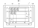
- FIG. 1 is a schematic diagram showing an example of a schematic configuration of a display device according to an embodiment of the present disclosure
- FIG. 2 is a schematic circuit diagram showing an equivalent circuit of an example of the pixel circuit shown in FIG. 1
- FIG. 3 is a schematic diagram showing an example of behavior of the pixel circuit shown in FIG. 2
- FIG. It is a schematic diagram which shows an example of schematic structure of organic LED.
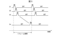
- 2 is a schematic diagram showing an example of signal potentials supplied to the scanning lines shown in FIG. 1
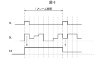
- FIG. 3 is a schematic diagram showing an example of behavior of the pixel circuit shown in FIG. 2;
- FIG. 4 is a schematic circuit diagram showing an equivalent circuit of a pixel circuit of a comparative example
- 8 is a schematic diagram showing an example of the behavior of the pixel circuit of the comparative example shown in FIG. 7
- FIG. FIG. 4 is a diagram showing characteristics of a TFT having an n-type channel made of an oxide semiconductor
- 3 is a schematic circuit diagram showing a circuit configuration in which an equivalent circuit between the gate and source of a drive transistor DR-T is added to the equivalent circuit of the pixel circuit of the comparative example
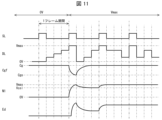
- FIG. 11 is a schematic diagram showing an example of the behavior of the pixel circuit of the comparative example shown in FIG. 10
- FIG. 2 is a schematic circuit diagram showing an equivalent circuit of an example of the pixel circuit shown in FIG. 1;
- FIG. 13 is a schematic diagram showing an example of behavior of the pixel circuit shown in FIG. 12;
- FIG. FIG. 4 is a schematic diagram showing an equivalent circuit of a pixel circuit of a comparative example;
- 2 is a schematic circuit diagram showing an equivalent circuit of an example of the pixel circuit shown in FIG. 1;
- FIG. 1 is a schematic diagram showing an example of a schematic configuration of a display device according to an embodiment of the present disclosure;
- FIG. 18 is a schematic circuit diagram showing an equivalent circuit of an example of the pixel circuit shown in FIG. 17;
- FIG. 19 is a schematic diagram showing an example of the behavior of the pixel circuit shown in FIG. 18;
- FIG. 19 is a schematic diagram showing an example of the behavior of the pixel circuit shown in FIG. 18;
- FIG. 19 is a schematic diagram showing an example of the behavior of the pixel circuit shown in FIG. 18;
- FIG. 4 is a schematic diagram showing an example of behavior of a pixel circuit in a frame period of 0 gradation;
- FIG. 4 is a schematic diagram illustrating an example of behavior of a pixel circuit during a frame period of a maximum luminance gray scale; It is a figure which shows the relationship between time and APL.
- FIG. 1 is a schematic diagram showing an example of a schematic configuration of a display device 2 according to an embodiment of the present disclosure.
- the display device 2 includes a display section DA including n scanning lines SL, n control lines PudL, m data signal lines DL, and m*n pixel circuits PC, a scan driver SD (driving circuit) for driving the scanning lines SL, a pump up-down driver PudD (driving circuit) for driving the control lines PudL, a data driver DD for driving the data signal lines DL, and a power supply potential Vdd for a pixel current supply source.
- a power supply potential wiring VddL and a common reference potential wiring VssL for supplying the common reference potential Vss of the pixel current supply source are provided.
- n is an integer of 2 or more
- m is an integer of 2 or more
- "*" is used as an operator for accumulation.
- the scanning lines SL extend in the horizontal direction and are supplied with scanning signals for controlling writing to the pixel circuits PC.
- the i-th scanning line SL is connected to the output terminal Si of the scanning driver SD.
- i is an integer less than or equal to n.
- the control line PudL extends in the same horizontal direction as the scanning line SL, and is supplied with a pulse signal.
- the control line PudL of the i-th stage is connected to the output terminal Pi of the pump up-down driver PudD.
- the data signal line DL extends in the vertical direction and supplies a write data signal to the pixel circuit PC.
- the data signal line DL intersects the scanning line SL and the control line PudL perpendicularly in a plan view, and is provided in a separate layer from the scanning line SL and the control line PudL. Therefore, the data signal line DL is not connected to the scanning line SL and the control line PudL.
- the j-th row data signal line DL is connected to the output terminal Dj of the data driver DD.
- j is an integer less than or equal to m.
- the power supply potential wiring VddL and the common reference potential wiring VssL are power lines for supplying current to the light emitting element Ed, and are constant potential wirings.
- Common reference potential Vss may be GND potential or ground potential.
- the common reference potential Vss is set to 0V.
- the pixel circuits PC are arranged in a matrix so as to correspond to the intersections of the scanning lines SL and the data signal lines DL, and are connected to the corresponding scanning lines SL, the corresponding data signal lines DL, and the corresponding control lines PudL.
- the pixel circuit PC provided in the i-th row and j-th row is connected to the output terminal Si of the scan driver SD via the i-th scanning line SL, to the output terminal Pi of the pump up-down driver PudD via the i-th control line PudL, and to the output terminal Dj of the data driver DD via the j-th row data signal line DL.
- FIG. 2 is a schematic circuit diagram showing an equivalent circuit of one example of the pixel circuit PC shown in FIG.
- FIG. 3 is a schematic diagram showing an example of behavior of the pixel circuit PC shown in FIG.
- the pixel circuit PC includes a light emitting element Ed, a drive transistor DR-T, a write control transistor SW-T, a first capacitor Csb, and a second capacitor Csa.
- the light-emitting element Ed may be an organic light-emitting diode (OLED) including an organic light-emitting layer or a quantum dot diode (QLED) including a quantum dot light-emitting layer.
- OLED organic light-emitting diode
- QLED quantum dot diode
- the light emitting element Ed is connected between the power supply potential wiring VddL and the common reference potential wiring VssL.
- the drive transistor DR-T is connected in series with the light emitting element Ed between the power supply potential wiring VddL and the common reference potential wiring VssL, and controls the amount of current flowing through the light emitting element Ed.
- the drive transistor DR-T is a thin film transistor (TFT) with an n-type channel.
- the write control transistor SW-T has a gate terminal connected to the corresponding scanning line SL, and is connected between the corresponding data signal line DL and the gate terminal of the drive transistor DR-T.
- the first capacitor Csb has a first electrode connected to the gate terminal of the drive transistor DR-T and the write control transistor SW-T, and a second electrode connected to the constant potential wiring.
- the second electrode is connected to the power supply potential wiring VddL. Data signals are sequentially written into the first capacitors Csb from the corresponding data signal lines DL via the write control transistors SW-T.
- the second capacitor Csa has a first electrode connected to the gate terminal of the drive transistor DR-T, the write control transistor SW-T, and the first electrode of the first capacitor Csb, and a second electrode connected to the corresponding control line PudL. Data signals are sequentially written from the corresponding data signal line DL to the second capacitor Csa via the write control transistor SW-T.
- circuit configuration shown in FIG. 2 merely shows the minimum required circuit configuration for the basic operation of the pixel circuit PC.
- additional transistors are provided to control the current in order to compensate for variations in circuit elements.
- a pulse signal is supplied to the scanning line SL and the control line PudL, and a stepped data voltage is supplied to the data signal line DL. Then, the potential of the node N1 connected to the gate terminal of the driving transistor DR-T of the pixel circuit PC fluctuates as shown in FIG. As a result, the luminance of the light emitting element Ed of the pixel circuit PC fluctuates as shown in FIG.
- the light emission luminance of the light emitting element Ed is controlled by the current flowing between the source and drain of the drive transistor DR-T.
- the current flowing between the source and drain of the drive transistor DR-T is controlled by the potential difference between the gate and source of the drive transistor DR-T.
- the potential difference between the gate and source of the drive transistor DR-T is controlled by the charges accumulated in the first capacitor Csb and the second capacitor Csa and the potential of the control line PudL.
- the signal potential supplied to the scanning line SL becomes the potential Vslh (so-called "ON potential") that makes the write control transistor SW-T conductive.
- Vslh the potential that makes the write control transistor SW-T conductive.
- Charge corresponding to the potential 0V or Vmax of the data signal line DL at that time is stored in the first capacitor Csb and the second capacitor Csa, and the luminance of the light emitting element Ed is controlled during the frame period.
- the display device 2 may be a Micro LED display.
- a portion of the pixel circuit PC shown in FIG. 2 excluding the light emitting element Ed, an electrode pad for connecting the micro LED, a scanning line SL, a control line PudL, a data signal line DL, a power supply potential wiring VddL, and a common reference potential wiring VssL are provided on the supporting substrate.
- the support substrate is a glass substrate or the like.
- the light emitting element Ed is externally mounted on the support substrate as a micro LED.
- LED means light emitting diode
- the display device 2 may be an organic LED display.
- a portion of the pixel circuit PC shown in FIG. 2 excluding the light emitting element Ed, the scanning line SL, the control line PudL, the data signal line DL, and the power supply potential wiring VddL are provided on the supporting substrate.
- a transparent electrode functioning as a common reference potential wiring VssL is provided on the opposing substrate, and an organic LED is generated between the supporting substrate and the opposing substrate.
- FIG. 4 is a schematic diagram showing an example of the schematic configuration of an organic LED.
- the organic LED consists of a laminate of a cathode 12, an electron injection layer 14, an electron transport layer 16, a light emitting layer 18, a hole transport layer 20, a hole injection layer 22, and an anode 24 formed on a support substrate 10.
- At least one of the cathode 12 and the anode 24 is a transparent electrode.
- the transparent electrode may be formed from a transparent conductor such as indium tin oxide (so-called “ITO”) or from a thin film of an opaque conductor such as a silver alloy.
- ITO indium tin oxide
- the display device 2 may be a liquid crystal display including a mini LED backlight.
- the above local dimming LED backlight mainly has a circuit configuration in which the output of the LED driver is connected to the cathode side of the mini LED for each area, and wiring and anode wiring corresponding to the number of areas are required.
- the number of areas increases, the number of wiring lines increases, and the same number of outputs of the LED drivers is required, so there is a problem that the number of LED drivers increases.
- active matrix driving in which pixel circuits including TFTs are formed on a glass substrate used in current liquid crystal panels, is considered to be a local dimming driving method. In the future, if the number of areas exceeds 10,000, active matrix driving will be effective.
- the support substrate is provided with a portion of the pixel circuit PC shown in FIG.
- the support substrate is a glass substrate or the like.
- the light emitting element Ed is externally mounted on the substrate as a mini LED.
- the light emitting element Ed may be a series of two or more LEDs. Two or more LEDs may be connected in parallel, in series, or in a parallel-series mixed connection.
- FIG. 5 is a schematic diagram showing an example of signal potentials supplied to the scanning line SL shown in FIG.
- FIG. 6 is a schematic diagram showing an example of behavior of the pixel circuit PC shown in FIG.
- the waveform representing the luminance of the light-emitting element Ed in FIG. 6 is merely a simplified step-like waveform for simplification of explanation. Furthermore, for simplicity of explanation, it should be understood that phenomena unrelated to the basic operation of active matrix driving, such as voltage effects due to leakage currents across the terminals of each transistor, have been omitted.
- the display device 2 is an active matrix driven display device.
- a certain period (so-called “frame period” or “vertical scanning period”) is divided by n, and a potential (so-called “ON potential”) is sequentially supplied to the scanning line SL to turn on the write control transistor SW-T.
- Each scanning line SL is supplied with a potential (so-called "OFF potential”) that causes the write control transistor SW-T to be in a non-conducting state after the period in which the ON potential is supplied (so-called "ON period”) ends.
- each data signal line DL is connected to the corresponding node N1 via the corresponding write control transistor SW-T, and applies voltage to the corresponding first capacitor Csb and the corresponding second capacitor Csa.
- Charge corresponding to the applied voltage is accumulated in the first capacitor Csb and the second capacitor Csa.
- the first capacitor Csb and the second capacitor Csa hold a voltage (so-called "data voltage") corresponding to the accumulated charge during a period (so-called "OFF period”) in which the scanning line SL is supplied with the OFF potential.
- the current flowing between the source and the drain of the driving transistor DR-T is controlled, and the luminance of the light emitting element Ed is controlled.
- FIG. 7 is a schematic circuit diagram showing an equivalent circuit of the pixel circuit 100 of Comparative Example 1. As shown in FIG.
- FIG. 8 is a schematic diagram showing an example of the behavior of the pixel circuit 100 of Comparative Example 1 shown in FIG.
- FIG. 9 is a diagram showing characteristics of a TFT having an n-type channel made of an oxide semiconductor.
- the vertical axis of FIG. 9 indicates the current Id flowing between the source and drain of the TFT, and the horizontal axis indicates the voltage Vgs between the gate and source of the TFT.
- FIG. 10 is a schematic circuit diagram showing a circuit configuration in which an equivalent circuit between the gate and source of the driving transistor DR-T is added to the equivalent circuit of the pixel circuit 100 of Comparative Example 1.
- FIG. 10 is a schematic circuit diagram showing a circuit configuration in which an equivalent circuit between the gate and source of the driving transistor DR-T is added to the equivalent circuit of the pixel circuit 100 of Comparative Example 1.
- FIG. 11 is a schematic diagram showing an example of the behavior of the pixel circuit 100 of Comparative Example 1 shown in FIG.
- the pixel circuit 100 of Comparative Example 1 is the same as the pixel circuit PC of Embodiment 1, except that it is not connected to the control line PudL and has a storage capacitor Cs instead of the first capacitor Cab and the second capacitor Csa. Note that the capacity of the storage capacity Cs is equal to the sum of the capacities of the first capacity Cab and the second capacity Csa.
- a dark display in which the light-emitting element Ed does not emit light continues for several frames, and then a stepwise signal potential is supplied to the scanning line SL and the data signal line DL so that the dark display is switched to a bright display in which the light-emitting element Ed emits light, and the luminance change of the light-emitting element Ed is measured.
- the luminance of the light emitting element Ed decreased over time.
- the luminance of the light emitting element Ed did not decrease over time.
- leakage current between the gate and source of the drive transistor DR-T was investigated as the cause of the decrease in brightness. However, if the leakage current is the cause, the luminance should have decreased similarly in the second and subsequent frame periods after switching. Therefore, it is inferred that leakage current is not the cause.
- Insufficient charging of the gate electrode of the drive transistor DR-T was also considered as the cause of the decrease in luminance.
- the length of the ON period is set sufficiently so that the storage capacitor Cs can hold the data voltage until the next frame period. Therefore, it is inferred that insufficient charging is not the cause.
- the drive transistor DR-T is a TFT with an n-type channel made of an oxide semiconductor such as indium gallium tin oxide
- Vgs a voltage generated between the gate and source of the drive transistor DR-T
- charges are accumulated in the p-type semiconductor facing the gate electrode with an insulator interposed therebetween.
- the potential difference between the gate and the source becomes equal to or higher than the threshold voltage Vth, the current Id flowing between the source and the drain rapidly increases.
- the depletion layer of a semiconductor holds charges unlike an insulator. Then, when the gate-source voltage Vgs is equal to or higher than the flat band voltage, the depletion layer of the semiconductor changes and a neutral region and an accumulation region are formed.
- the gate-source capacitance between the gate-source voltage Vgs of 0 V and a voltage smaller than the flat band voltage, there are the gate-source capacitance Cg due to the insulator and the capacitance Ct due to the state of the depletion layer of the semiconductor. Two capacitances Cg and Ct are connected in series.
- the gate-source voltage Vgs becomes equal to or higher than the flat band voltage, the state of the depletion layer in the semiconductor gradually changes, and the capacitance Ct caused by the depletion layer gradually disappears.
- the time required for the state change of the depletion layer is longer than the ON period during which the data voltage is written to the storage capacitor Cs.
- the voltage Vgs between the gate and source of the driving transistor DR-T is lower than the flat band voltage in dark display and is equal to or higher than the flat band voltage in bright display. For these reasons, it is necessary to consider the capacitance Ct due to the depletion layer immediately after switching from bright display to dark display.
- the capacitance Ct due to the depletion layer changes depending on the charge distribution due to the state of the depletion layer in the semiconductor. When the voltage Vgs changes from below the flat band to above the flat band, the state of the depletion layer changes with time.
- the state change speed of the depletion layer is estimated to be about sub ms to several ms from the change of the voltage Vgs to the completion of the state change, depending on the material and composition.
- the capacitance Ct due to the depletion layer exists and is proportional to the reciprocal of the square root of the voltage Vb.
- the depletion layer electrons and holes are thermally generated and annihilated repeatedly.
- electrons in the depletion layer gradually move to the interface with the insulator, and the thickness of the depletion layer gradually decreases. Since this phenomenon is a transition to a thermal equilibrium state, it takes time from sub ms to several ms. After the transition, there is no need to consider the capacitance Ct.
- an equivalent circuit between the gate and source of the drive transistor DR-T is added to the pixel circuit 100 of Comparative Example 1.
- the capacitance Cg is the capacitance due to the insulator between the gate and the source
- the capacitance Ct is the capacitance dependent on the state of the semiconductor
- Rt is the resistance that expresses the nonlinear dielectric relaxation due to the state transition of the semiconductor as a simple charge flow. Note that the capacitance Ct and the resistance Rt are not constants, but vary according to the gate-source voltage Vgs.
- the capacitance Cgf between the gate and source of the drive transistor DR-T is the combined capacitance of the two directly connected capacitances Cg and Ct.
- a stepwise signal potential is supplied to the scanning line SL and the data signal line DL so that the dark display is switched to the bright display after the dark display continues for several frame periods.
- the capacitance Cgf between the gate and source of the drive transistor DR-T, the potential of the node N1, and the luminance of the light emitting element Ed change as shown in FIG.
- an ON potential is applied to the scanning line SL every frame period.
- the potential of the data signal line DL is held in the storage capacitor Cs, and the potential of the node N1 is equal to the potential of the data signal line DL.
- the potential of the data signal line DL is 0 V during the ON period of the first frame period among the frame periods shown in FIG. 11, and is Vmax during the ON period of the second and subsequent frame periods.
- the gate-source capacitance Cgf of the drive transistor DR-T is equivalent to the capacitance Cg due to the insulator during the frame period during which the dark display continues and the frame period during which the bright display continues.
- the potential Vcs of the node N1 changes from Vmax to Vcsl as the capacitance Cgf returns from Cgo to Cg in the frame period immediately after switching from dark display to bright display.
- the light emission luminance of the light emitting element Ed is proportional to the source-drain current Id of the drive transistor DR-T, and the drive transistor DR-T has a range in which the current Id changes greatly according to the change in the gate-source voltage Vgs as described above. Therefore, in such a range, even if the gate-source voltage Vgs changes by several percent, the change in luminance is large.
- Vscl is about 92.7% of Vmax. If Vmx is 5.0V, Vcxl is approximately 4.67V. Therefore, even if the storage capacity Cs is ten times the electrostatic capacity Cg of the insulator, it is estimated that the potential of the node N1, ie, the voltage Vgs between the gate and source of the drive transistor DR-T, will drop by about 7%.
- the cause of the decrease in brightness is the change in the capacitance Cgf between the gate and source of the driving transistor DR-T.
- the decrease in luminance can also be eliminated by sufficiently charging the storage capacitance Cs, which is large enough to prevent its influence.
- the resolution of the screen is increasing, the pixel area is limited to a small size, and the ON time is limited to a short period. For this reason, the storage capacity Cs cannot be sufficiently enlarged.
- the pixel circuit PC includes the second capacitor Csa, and the second electrode of the second capacitor Csa is connected to the corresponding control line PudL. Therefore, as shown in FIG. 3, when the potential of the control line PudL is raised from the low potential Vudl (first level potential) to the high potential Vudh (second level potential) after the ON period, the potential Vcs of the node N1 is raised via the second capacitor Csa.
- ⁇ Vcs be the voltage width by which the potential Vcs of the node N1 is raised
- ⁇ C be the sum of all capacitances connected to the node N1
- ⁇ Vcs Csa/ ⁇ C*Vamp.
- the total capacitance ⁇ C includes the first capacitance Csb, the second capacitance Csa, the capacitance Cgf between the gate and source of the drive transistor DR-T, and parasitic capacitance other than between the gate and source of the drive transistor DR-T.
- the pull-up voltage width ⁇ Vcs immediately after writing that switches from dark display to bright display is larger than the pull-up voltage width ⁇ Vcs immediately after writing that continues bright display. Then, it is possible to compensate or cancel the potential change of the node N1 due to the change of the capacitance Cgf between the gate and source of the driving transistor DR-T. Therefore, compared to the pixel circuit 100 of Comparative Example 1, it is possible to reduce the decrease in luminance of the light emitting element Ed in the frame period immediately after switching from bright display to dark display.
- the timing at which the potential of the pulse signal of the control line PudL rises from the low potential Vudl (first level) to the high potential Vudh (second level) is from the end of writing the data signal to the corresponding pixel circuit PC to the start of writing the next data signal.
- the capacitance Cgf between the gate and the source is Cgo immediately after writing to switch from dark display to bright display, and gradually returns to Cg. Therefore, it is desirable to raise the potential of the control line PudL immediately after writing to switch from dark display to bright display.
- the timing at which the pulse signal of the control line PudL rises from the low potential Vudl (first level) to the high potential Vudh (second level) is preferably in the period from the end of writing the data signal to the corresponding pixel circuit PC to the end of writing the data signal to the next-stage pixel circuit PC of the corresponding pixel circuit PC.
- Tp the time from the end of the ON period of the corresponding pixel circuit PC to the timing of boosting the potential of the control line PudL from Vudl to Vudh.
- the timing at which the potential of the pulse signal of the control line PudL drops from the high potential Vudh (second level) to the low potential Vudl (first level) is preferably in the ON period during which the data signal is written to the corresponding pixel circuit PC.
- the pull-up voltage width ⁇ Vcs is larger than the threshold voltage Vth of the drive transistor DR-T, the light emitting element Ed can emit light during the dark display frame period. This is because 0 V is written to the first capacitor Csb and the second capacitor Csa during the ON period of the dark display frame period, and immediately after the writing, the potential Vcs of the node N1 is raised higher than the threshold voltage Vth by raising the potential of the control line PudL. Therefore, the potential amplitude Vamp and the pull-up timing of the control line PudL are set so that the pull-up voltage width ⁇ Vcs is equal to or less than the threshold voltage Vth. From the viewpoint of efficiency, it is desirable to set the pull-up voltage width ⁇ Vcs to a voltage as close as possible to the threshold voltage Vth.
- the potential amplitude Vamp and the pull-up timing of the control line PudL so that the average luminance of the light emitting element Ed in the frame period immediately after switching from dark display to bright display is equivalent to the average luminance of the light emitting element Ed in the frame period in which the bright display continues.
- the potential supplied from the data signal line DL during the ON period of the frame period immediately after switching from the dark display to the bright display is equivalent to the potential supplied from the data signal line DL during the ON period of the frame period during which the bright display continues.
- the drive transistor DR-T should be set so that the data voltage Vmax that maximizes the current Id flowing between the source and drain of the drive transistor DR-T is 2.16 times the threshold voltage Vth. At this time, the decrease in luminance during the frame period immediately after switching from dark display to bright display is reduced.
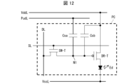
- FIG. 12 is a schematic circuit diagram showing an equivalent circuit of one example of the pixel circuit PC shown in FIG.
- FIG. 13 is a diagram showing characteristics of a TFT having a p-type channel made of an oxide semiconductor.
- the vertical axis of FIG. 13 indicates the current Id flowing between the source and drain of the TFT, and the horizontal axis indicates the voltage Vgs between the gate and source of the TFT.
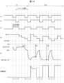
- FIG. 14 is a schematic diagram showing an example of behavior of the pixel circuit PC shown in FIG.
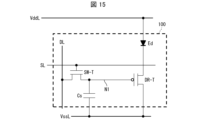
- FIG. 15 is a schematic diagram showing an equivalent circuit of the pixel circuit 200 of Comparative Example 2.
- FIG. 15 is a schematic diagram showing an equivalent circuit of the pixel circuit 200 of Comparative Example 2.
- the pixel circuit PC according to the present embodiment is the same as the pixel circuit PC according to Embodiment 1 described above, except that the driving transistor DR-T is a TFT having a p-type channel, and accordingly the second electrode of the second capacitor Csa is connected to the common reference potential line VssL.
- the data voltage supplied to the data signal line DL is the power supply potential Vdd supplied by the power supply potential wiring VddL during dark display.
- the data voltage that maximizes the current Id flowing between the source and drain of the drive transistor DR-T is Vmin.
- the pixel circuit 200 of Comparative Example 2 is the same as the pixel circuit PC of Embodiment 2, except that it is not connected to the control line PudL and has a storage capacitor Cs instead of the first capacitor Cab and the second capacitor Csa. Note that the capacity of the storage capacity Cs is equal to the sum of the capacities of the first capacity Cab and the second capacity Csa.
- the luminance of the light emitting element Ed decreased over time in the frame period immediately after switching from dark display to bright display.
- the pixel circuit PC compared with the pixel circuit 200 of Comparative Example 2, it is possible to reduce the decrease in luminance of the light emitting element Ed in the frame period immediately after switching from bright display to dark display.
- Tp is the period from the end of the ON period of the corresponding pixel circuit PC to the timing of stepping down the potential of the control line PudL from the high potential Vudh (first level potential) to the low potential Vudl (second level potential)
- the time Tp be as short as possible. That is, it is desirable that Tp>0 and Tp ⁇ 0.
- the timing for boosting the potential of the control line PudL from Vudl to Vudh is preferably the ON period of the corresponding pixel circuit PC.
- the voltage width by which the potential Vcs of the node N1 is lowered is ⁇ Vcs, and the potential amplitude Vamp and the pull-up timing of the control line PudL are set so that the absolute value of the pull-down voltage width ⁇ Vcs is equal to or less than the absolute value of the threshold voltage Vth. From the viewpoint of efficiency, it is desirable to set the voltage drop width ⁇ Vcs to a voltage as close as possible to the threshold voltage Vth.
- the parameters are set by the same method as in the first embodiment, taking into consideration the fact that the magnitude relationship of the voltages related to the drive transistor DR-T is inverted.
- FIG. 16 is a schematic circuit diagram showing an equivalent circuit of one example of the pixel circuit PC shown in FIG.
- the pixel circuit PC according to this embodiment is the same as the pixel circuit PC according to Embodiment 1 described above, except that the drive transistor DR-T is a metal oxide semiconductor field effect transistor (MOSFET).
- MOSFET metal oxide semiconductor field effect transistor
- the MOSFET is formed separately from the support substrate. Therefore, an electrode pad for connecting the driving transistor DR-T is provided on the support substrate instead of the driving transistor DR-T.
- the drive transistor DR-T is mounted externally on the support substrate.
- the pixel circuits 100 and 200 of Comparative Examples 1 and 2 described above experience a decrease in luminance during the frame period immediately after switching from dark display to bright display.
- the mechanism of generation of the depletion layer in the semiconductor below the flat band voltage described above differs between TFT and MOSFET.
- the change in the state of the depletion layer in the semiconductor with respect to the transition of the gate voltage from below the flatband voltage to above the flatband voltage, which causes the luminance reduction occurs in the MOSFET as well as the TFT.
- the pixel circuit PC according to the present embodiment exhibits behavior similar to that of the pixel circuit PC according to the first embodiment.
- FIG. 17 is a schematic diagram showing an example of a schematic configuration of the display device 2 according to an embodiment of the present disclosure.
- the display device 2 includes a data timing controller DTC in addition to the same configuration as the display device 2 according to any one of the first to third embodiments.
- the data timing control unit DTC sends to the data driver DD a Data signal indicating an image in each frame period and a Dtim signal indicating data transfer timing.
- the data timing controller DTC sends to the scan driver SD the SST signal indicating the start of scanning, the SON signal indicating the ON period, and the SShift signal indicating the timing shift of the output.
- the data timing control unit DTC sends to the pump up/down driver PudD a PUST signal indicating the start timing of outputting up, a PDST signal indicating the start timing of outputting down, and a PShift signal indicating the timing shift of the output.
- the data driver DD outputs a data voltage corresponding to the Data signal from each output terminal D1 to Dm to each data signal line DL at a timing corresponding to the Dtim signal.
- An ON voltage Son and an OFF voltage Soff are also input to the scan driver SD.
- the scan driver SD outputs an ON voltage Son from the output terminal S1 of the first stage to the scanning line SL at a timing corresponding to the SST signal for a period corresponding to the SON signal, and then outputs an OFF voltage Soff.
- the scan driver SD outputs the ON voltage Son from the output terminal S2 of the second stage to the scanning line SL in a period corresponding to the SON signal at a timing shifted according to the SShift signal from the timing corresponding to the SST signal, and then outputs the OFF voltage Soff.
- the scan driver SD similarly outputs the ON voltage Son from the output terminals S1 to Sn of each stage to each scanning line SL at sequentially shifted timings.
- a high potential Vudh and a low potential Vudl are individually input to the pump up/down driver PudD.
- the pump up-down driver PudD outputs a high potential Vudh from the output terminal P1 of the first stage to the control line PudL from the timing indicated by the PUST signal to the timing indicated by the PDST signal, and outputs the low potential Vudl from the timing indicated by the PDST signal to the timing indicated by the PUST signal.
- the pump up-down driver PudD outputs a high potential Vudh or a low potential Vudl from the output terminals P1 to Pn of each stage to the corresponding control line PudL so as to sequentially shift the timing according to the Pshift signal.
- FIG. 18 is a schematic circuit diagram showing an equivalent circuit of one example of the pixel circuit PC shown in FIG. FIG. 18 shows the pixel circuit PC of the x-th row and the y-th row.
- a configuration in which the driving transistor DR-T is a TFT having a p-type channel will be described below, but a configuration in which the driving transistor DR-T is a TFT or a MOSFET having an n-type channel is also included in the scope of the present embodiment.
- the pixel circuit PC according to this embodiment is the same as the pixel circuit PC according to Embodiments 1 to 3 described above, except that an internal compensation circuit that compensates for variations in the threshold voltage Vth of the driving transistor DR-T is incorporated.
- the pixel circuit PC incorporates an internal compensation circuit including a set of isolation transistors R1-T and R2-T, a set of voltage initialization transistors R3-T and R4-T, and a compensation transistor RE-T in the pixel circuit PC according to Embodiments 1 to 3 described above.
- the isolation transistors R1-T and R2-T are arranged so as to isolate the drive transistor DR-T from the current path passing through the light emitting element Ed connected between the power supply potential wiring VddL and the common reference potential wiring VssL.
- the gate terminals of the isolation transistors R1-T and R2-T of the pixel circuit PC of the i-th stage are connected to the output terminal Ri of the i-th stage via the light emission control line RL.
- the voltage initialization transistors R3-T and R4-T are arranged so as to connect the first electrode of the first capacitor Csb and the first electrode of the second capacitor Csa to the reset voltage line VresL that supplies a constant voltage.
- the gate terminals of the voltage initialization transistors R3-T and R4-T of the i-th pixel circuit PC are connected to the output terminal S(i-1) in the same manner as the scanning line SL of the (i-1)th stage.
- the compensation transistor RE-T is arranged between the source terminal and the gate terminal of the drive transistor DR-T and connects them. Alternatively, the compensation transistor RE-T may be placed between and connected between the drain and gate terminals of the drive transistor DR-T.
- the gate terminal of the compensation transistor RE-T of the i-th pixel circuit PC is connected to the output terminal Si through the i-th scanning line SL.
- the data signal on the data signal line DL is written to the first capacitor Csb and the second capacitor Csa via the drive transistor DR-T and the compensation transistor RE-T, thereby compensating for variations in the threshold voltage Vth of the drive transistor DR-T.
- the drive transistor DR-T is disconnected from the current path through the light emitting element Ed by the disconnecting transistors R1-T and R2-T, so the light emitting element Ed does not emit light.
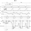
- FIGS. 19 to 21 are schematic diagrams each showing an example of the behavior of the pixel circuit PC on the x-th row and the y-th row shown in FIG.
- the pixel circuit PC in the x-th row and the y-th row is in dark display during the first frame period and several frame periods before it.
- the pixel circuit PC in the x-th row and the y-th row is brightly displayed at the maximum luminance gradation.
- FIG. 19 shows behavior when a constant potential is supplied to the control line PudL.
- the potential Vcs of the node N1 of the pixel circuit PC of the x-th stage is reset to the voltage Vres of the reset voltage line VresL while the output terminal Sx-1 for the scanning line SL of the (x-1)th stage is supplying the ON voltage Son.
- This period is referred to as a "reset period” or "x-stage reset period”.
- the output terminal Rx for the emission control line RLL of the x-th stage supplies an OFF voltage, and the light-emitting element Ed of the pixel circuit PC of the x-th stage is turned off.
- This period is called a "non-lighting period” or a “non-lighting period of x stages”.
- the data voltage output from the output terminal Dy to the pixel circuit PC during the dark display frame period is Vdd-V0. Since the data voltage is written to the first capacitor Csb and the second capacitor Csa via the drive transistor DR-T, the written voltage is lower than the data voltage by the threshold voltage Vth of the drive transistor DR-T. Therefore, the absolute value of the potential difference between the gate and source of the driving transistor DR-T at this time
- V0+Vth. Since V0 ⁇ 0V, the light emitting element Ed emits almost no light.
- the data voltage output from the output terminal Dy to the pixel circuit PC in the bright display frame period with the maximum luminance gradation is Vdd-Vmax.
- the voltage to be written is lower than the data voltage by the threshold voltage Vth of the drive transistor DR-T, and the absolute value of the potential difference between the gate and source of the drive transistor DR-T
- Vmax+Vth.
- the second frame period is a frame period during which there is a transition from almost non-emission to high gradation luminance. That is, in the second frame period, the state of the semiconductor of the drive transistor DR-T changes, so the absolute value
- the third and fourth frame periods are frame periods during which the high-gradation luminance continues. That is, in the third and fourth frame periods, the state of the semiconductor of the drive transistor DR-T is in an equilibrium state, the absolute value
- the luminance of the light-emitting element Ed decreases only in the first frame period during the transition from the low gradation luminance to the high gradation luminance, so the display response is delayed.
- FIG. 20 shows behavior when a pulse signal is supplied to the control line PudL.
- the signal potential output from the output terminal Px to the x-stage control line PudL shifts from the low potential Vudl to the high potential Vudh during the write period, and shifts from the high potential Vudh to the low potential Vudl after the write period ends.
- This transition of the potential of the control line PudL is similar to the transition of the potential of the control line PudL in the second embodiment described above.
- the potential Vcs of the node N1 drops significantly due to the lowering of the potential of the control line PudL. Therefore, even if the potential Vcs of the node N1 rises due to the transition of the state of the semiconductor, the average luminance of the light emitting element Ed increases. Therefore, as in the second embodiment, the voltage can be adjusted so that the average luminance in each frame period is the same, and the display response when transitioning from low gradation luminance to high gradation luminance is improved.
- the pixel circuit PC according to the present embodiment incorporates a circuit that compensates for the threshold voltage Vth, when driving the pixel circuit PC according to the present embodiment in the same manner as the pixel circuit PC according to the second embodiment, it is difficult to make the absolute value
- FIG. 20 shows the behavior when another pulse signal is supplied to the control line PudL.
- the potential of the pulse signal output from the output terminal Px to the control line PudL of the x stage maintains the high potential Vudh (first level) during the writing period of the data signal of the x stage, and shifts from the high potential Vudh (first level) to the low potential Vudl (second level) after the time Tp has elapsed from the end of the writing period of the x stage.
- the potential of the pulse signal from the output terminal Px shifts from the low potential Vudl (second level) to the high potential Vudh (first level) after the shift from the high potential Vudh (first level) to the low potential Vudl (second level) until the write period of the next data signal in the x stage is started.
- time Tq be the time required for the pulse signal shifted to the low potential Vudl (second level) to return to the high potential Vudh (first level).
- the time Tq is preferably longer than the time required for the state of the semiconductor of the drive transistor DR-T to shift to the equilibrium state.
- the time required to shift to the equilibrium state depends on the semiconductor material, impurity concentration, and temperature, but is estimated to be approximately several milliseconds.
- Vdd-V0-Vth is written to the potential Vcs of the node N1 during the writing period.
- the capacitive coupling of the second capacitor Csa lowers the potential Vcs of the node N1 to Vdd-V0-Vth-.DELTA.Vp.
- the absolute value of the gate-source voltage Vgs of the driving transistor DR-T at this time is
- the luminance after time Tq is 0 in the frame period of 0 gradation. Therefore, whitening of black pixels is improved.
- the width by which the potential Vcs of the node N1 is lowered after the time Tp is larger by ⁇ Vq than the width by which the potential Vcs of the node N1 is raised after the time Tq. Therefore, as in the first to third embodiments, the display response is improved when transitioning from low gradation luminance to high gradation luminance.
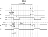
- FIG. 22 is a schematic diagram showing an example of the behavior of the pixel circuit PC during a frame period of 0 gradation.
- FIG. 23 is a schematic diagram showing an example of the behavior of the pixel circuit PC during the frame period of the gradation of maximum luminance.
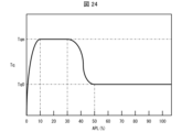
- FIG. 24 is a diagram showing the relationship between time Tp and APL (Average Picture Level).
- APL indicates the ratio of the total number of gradations of all pixels when displaying a certain image to the total number of gradations of all pixels when all pixels are at the maximum gradation.
- the gradation number is a data voltage that the data driver DD inputs from the output terminals D1 to Dm to the pixel circuit PC through the data signal line DL. That is, APL is calculated by the following formula.
- Di,j is the data voltage input to the pixel circuit PC of the i-th row and the j-th row when displaying a certain image.
- Dmax is a data voltage input to the pixel circuit PC when the pixel circuit PC causes the light emitting element Ed to emit light with the maximum luminance grayscale.
- ⁇ is used as a summation symbol.
- n is the number of scanning lines SL and is an integer of 2 or more.
- m is the number of data signal lines DL and is an integer of 2 or more.
- "*" is used as an operator for accumulation.
- the pulse width corresponding to the length of time Tp may be set according to the image to be displayed. That is, the pulse width of the pulse signal of the control line PudL may be set according to the input image data and data signal.
- the potential of the control line PudL is stepped down from the high potential Vudh to the low potential Vudl after the time Tp of the write period, and further increased from the low potential Vudl to the high potential Vudh after the time Tq.
- the light-emitting element Ed emits light, albeit a little, during the time Tq during which the potential of the control line PudL is at the low potential Vudl. As a result, black pixels appear white.
- the luminance of the light-emitting element Ed increases by the amount that the potential Vcs of the node N1 is lowered during the time Tq during which the potential of the control line PudL is at the low potential Vudl. After that, when the potential of the control line PudL returns to the high potential Vudh, the luminance of the light emitting element Ed decreases by the amount of the increased potential Vcs of the node N1. Therefore, compared to the pixel circuit PC according to the second embodiment, the average luminance of the light emitting element Ed during the frame period of the same gradation is low. Also, the longer the time Tq, the higher the average luminance of the light emitting element Ed.
- a shorter time Tq for dark display and a longer time Tq for high luminance display lead to improved display.
- the pulse width corresponding to the time Tq when displaying the first image is longer than the pulse width corresponding to the time Tq when displaying the second image darker than the first image.
- the length of the time Tq is changed according to the input image, thereby improving the whitening of black pixels and increasing the maximum luminance.
- the length of time Tq may be controlled according to APL.
- Tq 0 ms.
- the length of the time Tq may be controlled according to ALL (Average Luminance Level).
- the genre of the image to be displayed may be specified by ALL, and the length of the time Tq may be controlled according to the genre.
- ALL indicates the ratio of the total display luminance value of all pixels when displaying a certain image to the total display luminance value of all pixels when all pixels are at the maximum gradation.
- the display luminance value is a luminance value when the pixel circuit PC causes the light emitting element Ed to emit light in response to the data voltage input to the pixel circuit PC by the data driver DD. That is, ALL is calculated by the following formula.
- Li,j is the luminance value of the light emitting element Ed connected to the pixel circuit PC of the i-th row and the j-th row when displaying a certain image.
- Lmax is the luminance value of the light emitting element Ed when the pixel circuit PC causes the light emitting element Ed to emit light at the maximum luminance gradation.
- ⁇ is used as a summation symbol.
Landscapes
- Engineering & Computer Science (AREA)
- Physics & Mathematics (AREA)
- Computer Hardware Design (AREA)
- General Physics & Mathematics (AREA)
- Theoretical Computer Science (AREA)
- Control Of Indicators Other Than Cathode Ray Tubes (AREA)
Abstract
Description
(表示装置の構成)
図1は、本開示の一実施形態に係る表示装置2の概略構成の一例を示す模式図である。
図2は、図1に示した画素回路PCの一例の等価回路を示す概略回路図である。
表示装置2がマイクロLEDディスプレイであってよい。この場合、支持基板の上に図2に示した画素回路PCの発光素子Edを除く部分と、マイクロLEDを接続するための電極パッドと、走査線SLと制御線PudLとデータ信号線DLと電源電位配線VddLと共通基準電位配線VssLと、が設けられる。支持基板はガラス基板などである。発光素子Edは、マイクロLEDとして支持基板上に外付けされる。
表示装置2が有機LEDディスプレイであってもよい。この場合、支持基板の上に図2に示した画素回路PCの発光素子Edを除く部分と、走査線SLと制御線PudLとデータ信号線DLと電源電位配線VddLと、が設けられる。そして、対向基板の上に共通基準電位配線VssLとして機能する透明電極が設けられ、支持基板と対向基板との間に有機LEDが生成される。
表示装置2がミニLEDバックライトを含む液晶ディスプレイであってもよい。
図5は、図1に示した走査線SLに供給される信号電位の一例を示す概略図である。
図7は、比較例1の画素回路100の等価回路を示す概略回路図である。
図2を参照して示したように、本実施形態に係る画素回路PCは、第2容量Csaを備え、第2容量Csaの第2の電極が対応する制御線PudLに接続する。このため、図3に示すように、ON期間の後に制御線PudLの電位が低電位Vudl(第1レベルの電位)から高電位Vudh(第2レベルの電位)に引き上げられるとき、ノードN1の電位Vcsが第2容量Csaを介して引き上げられる。ノードN1の電位Vcsが引き上げられる電圧の幅をΔVcsとし、ノードN1に接続されている全ての静電容量の総和をΣCとし、制御線PudLの電位振幅をVamp(=Vudh-Vudl)とする。ΔVcs=Csa/ΣC*Vampである。静電容量の総和ΣCは、第1容量Csbおよび第2容量Csaと、駆動トランジスタDR-Tのゲートソース間の静電容量Cgfとに加えて、駆動トランジスタDR-Tのゲートソース間以外に寄生する静電容量を含む。
引き上げ電圧幅ΔVcsが駆動トランジスタDR-Tの閾値電圧Vthよりも大きい場合、暗表示のフレーム期間において、発光素子Edが発光し得る。なぜならば、暗表示のフレーム期間のON期間において、第1容量Csbおよび第2容量Csaに0Vが書き込まれ、書き込みの直後に制御線PudLの電位の引き上げによって、ノードN1の電位Vcsが閾値電圧Vthよりも大きく引き上げられるからである。したがって、引き上げ電圧幅ΔVcsが閾値電圧Vth以下であるように、制御線PudLの電位振幅Vampおよび引き上げタイミングを設定する。効率性の観点から、引き上げ電圧幅ΔVcsは、閾値電圧Vthになるべく近い電圧になるように、設定することが望ましい。
本発明の他の実施形態について、以下に説明する。なお、説明の便宜上、上記実施形態にて説明した部材と同じ機能を有する部材については、同じ符号を付記し、その説明を繰り返さない。
本発明の他の実施形態について、以下に説明する。なお、説明の便宜上、上記実施形態にて説明した部材と同じ機能を有する部材については、同じ符号を付記し、その説明を繰り返さない。
本発明の他の実施形態について、以下に説明する。なお、説明の便宜上、上記実施形態にて説明した部材と同じ機能を有する部材については、同じ符号を付記し、その説明を繰り返さない。
図17は、本開示の一実施形態に係る表示装置2の概略構成の一例を示す模式図である。
図18は、図17に示した画素回路PCの一例の等価回路を示す概略回路図である。図18は、第x段第y行の画素回路PCを示す。
図19~図21は各々、図18に示した第x段第y行の画素回路PCの挙動の一例を示す概略図である。図19~図21の各々において、1番目のフレーム期間およびそれ以前の数フレーム期間において、第x段第y行の画素回路PCは暗表示である。2番目のフレーム期間およびそれ以降の数フレーム期間において、第x段第y行の画素回路PCは最大輝度の階調での明表示である。
図22は、0階調のフレーム期間における画素回路PCの挙動の一例を示す概略図である。


Csb 第1容量
DA 表示部
DL データ信号線
DR-T 駆動トランジスタ
Ed 発光素子
SL 走査線
PC 画素回路
PudL 制御線
PudD ポンプアップダウンドライバ(駆動回路)
RE-T 補償トランジスタ
SD スキャンドラバ(駆動回路)
SW-T 書き込み制御トランジスタ
Tp 時間(第2レベルにシフトしたパルス信号が第1レベルに戻るまでの時間)
VddL 電源電位配線(定電位配線)
VssL 共通基準電位配線(定電位配線)
Vth 閾値電圧
Vudh 高電位(第2レベルの電位,第1レベルの電位)
Vudl 低電位(第1レベルの電位,第2レベルの電位)
Claims (17)
- 複数の走査線、複数の制御線、および、複数の画素回路を含む表示部と、
前記走査線および前記制御線を駆動する駆動回路とを備え、
前記画素回路は、
発光素子と、
前記発光素子と直列に設けられ、前記発光素子に流れる電流の量を制御する駆動トランジスタと、
ゲート端子が前記複数の走査線の対応する1本に接続する書き込み制御トランジスタと、
第1の電極が前記駆動トランジスタのゲート端子と前記書き込み制御トランジスタとに接続し、第2の電極が定電位配線に接続し、データ信号が順次書き込まれる第1容量と、
第1の電極が前記駆動トランジスタのゲート端子と前記第1容量の第1の電極とに接続し、第2の電極が前記複数の制御線の対応する1本に接続する第2容量を備え、
前記制御線には、パルス信号が供給される表示装置。 - データ信号の書き込み完了から次のデータ信号の書き込み開始までの間に、前記パルス信号が第1レベルから第2レベルへシフトする、請求項1に記載の表示装置。
- 画素回路への書き込み終了から次段の画素回路への書き込み終了までの期間に、前記パルス信号が第1レベルから第2レベルへシフトする、請求項2に記載の表示装置。
- 前記データ信号の書き込みが開始した後に、前記パルス信号が第2レベルから第1レベルへシフトする、請求項2または3に記載の表示装置。
- 前記データ信号の書き込み中は、前記パルス信号が第1レベルを維持し、
前記データ信号の書き込みが完了した後に、前記パルス信号が第1レベルから第2レベルへシフトし、
前記パルス信号が第1レベルから第2レベルへシフトした後から、次のデータ信号の書込みが開始されるまでの間に、前記パルス信号が第2レベルから第1レベルへシフトする、請求項1~3の何れか1項に記載の表示装置。 - 各画素回路は、駆動トランジスタの閾値電圧を補償する内部補償回路を含む、請求項5に記載の表示装置。
- 第2レベルにシフトしたパルス信号が第1レベルに戻るまでの時間に対応するパルス幅が、表示する画像に応じて設定される、請求項6に記載の表示装置。
- 入力される画像データに応じて前記パルス幅が設定される、請求項7に記載の表示装置。
- 第1画像を表示する際の前記パルス幅が、前記第1画像よりも暗い第2画像を表示する際の前記パルス幅よりも長く設定される、請求項7または8に記載の表示装置。
- 前記内部補償回路は補償トランジスタを含み、
前記駆動トランジスタのドレイン端子およびゲート端子が、あるいは、前記駆動トランジスタのソース端子およびゲート端子が、前記補償トランジスタを介して接続される請求項6~9の何れか1項に記載の表示装置。 - 前記発光素子は、前記データ信号の書き込み中に発光しない、請求項1~10のいずれか1項に記載の表示装置。
- 前記複数の制御線と、前記複数の走査線とが同方向に延伸する、請求項1~11の何れか1項に記載の表示装置。
- 前記第1レベルの電位と前記第2レベルの電位との差が、前記駆動トランジスタの閾値電圧以下である、請求項2~4の何れか1項に記載の表示装置。
- データ信号が供給される複数のデータ信号線を備え、
前記書き込み制御トランジスタは、前記複数のデータ信号線の対応する1本と前記駆動トランジスタとの間に接続される、請求項1~13の何れか1項に記載の表示装置。 - 前記駆動トランジスタがn型チャネルであり、前記第2レベルの電位が前記第1レベルの電位よりも高い、請求項2~4の何れか1項に記載の表示装置。
- 前記駆動トランジスタがp型チャネルであり、前記第2レベルの電位が前記第1レベルの電位よりも低い、請求項2~4の何れか1項に記載の表示装置。
- 前記発光素子は、有機発光層または量子ドット発光層を含む、請求項1~16のいずれか1項に記載の表示装置。
Priority Applications (2)
| Application Number | Priority Date | Filing Date | Title |
|---|---|---|---|
| US18/700,479 US20250232721A1 (en) | 2022-01-24 | 2022-01-24 | Display device |
| PCT/JP2022/002447 WO2023139792A1 (ja) | 2022-01-24 | 2022-01-24 | 表示装置 |
Applications Claiming Priority (1)
| Application Number | Priority Date | Filing Date | Title |
|---|---|---|---|
| PCT/JP2022/002447 WO2023139792A1 (ja) | 2022-01-24 | 2022-01-24 | 表示装置 |
Publications (1)
| Publication Number | Publication Date |
|---|---|
| WO2023139792A1 true WO2023139792A1 (ja) | 2023-07-27 |
Family
ID=87348410
Family Applications (1)
| Application Number | Title | Priority Date | Filing Date |
|---|---|---|---|
| PCT/JP2022/002447 Ceased WO2023139792A1 (ja) | 2022-01-24 | 2022-01-24 | 表示装置 |
Country Status (2)
| Country | Link |
|---|---|
| US (1) | US20250232721A1 (ja) |
| WO (1) | WO2023139792A1 (ja) |
Citations (6)
| Publication number | Priority date | Publication date | Assignee | Title |
|---|---|---|---|---|
| JP2004029791A (ja) * | 2002-06-11 | 2004-01-29 | Samsung Sdi Co Ltd | 発光表示装置及びその表示パネルと駆動方法 |
| JP2007065218A (ja) * | 2005-08-30 | 2007-03-15 | Eastman Kodak Co | アクティブマトリクス型表示装置 |
| JP2009251590A (ja) * | 2008-04-03 | 2009-10-29 | Samsung Mobile Display Co Ltd | 画素および有機電界発光表示装置 |
| JP2009294508A (ja) * | 2008-06-06 | 2009-12-17 | Sony Corp | 表示装置、表示装置の駆動方法および電子機器 |
| JP2011175103A (ja) * | 2010-02-24 | 2011-09-08 | Sony Corp | 画素回路、表示装置およびその駆動方法ならびに電子機器 |
| JP2013083825A (ja) * | 2011-10-11 | 2013-05-09 | Seiko Epson Corp | 電気光学装置、電気光学装置の駆動方法および電子機器 |
-
2022
- 2022-01-24 WO PCT/JP2022/002447 patent/WO2023139792A1/ja not_active Ceased
- 2022-01-24 US US18/700,479 patent/US20250232721A1/en active Pending
Patent Citations (6)
| Publication number | Priority date | Publication date | Assignee | Title |
|---|---|---|---|---|
| JP2004029791A (ja) * | 2002-06-11 | 2004-01-29 | Samsung Sdi Co Ltd | 発光表示装置及びその表示パネルと駆動方法 |
| JP2007065218A (ja) * | 2005-08-30 | 2007-03-15 | Eastman Kodak Co | アクティブマトリクス型表示装置 |
| JP2009251590A (ja) * | 2008-04-03 | 2009-10-29 | Samsung Mobile Display Co Ltd | 画素および有機電界発光表示装置 |
| JP2009294508A (ja) * | 2008-06-06 | 2009-12-17 | Sony Corp | 表示装置、表示装置の駆動方法および電子機器 |
| JP2011175103A (ja) * | 2010-02-24 | 2011-09-08 | Sony Corp | 画素回路、表示装置およびその駆動方法ならびに電子機器 |
| JP2013083825A (ja) * | 2011-10-11 | 2013-05-09 | Seiko Epson Corp | 電気光学装置、電気光学装置の駆動方法および電子機器 |
Also Published As
| Publication number | Publication date |
|---|---|
| US20250232721A1 (en) | 2025-07-17 |
Similar Documents
| Publication | Publication Date | Title |
|---|---|---|
| US20250246146A1 (en) | Pixel Circuit and Display Panel | |
| CN113838419B (zh) | 像素电路及其驱动方法、显示面板 | |
| US11631369B2 (en) | Pixel circuit and driving method thereof, display panel | |
| US10475377B2 (en) | Display device and method of driving the same | |
| KR101202040B1 (ko) | 유기발광다이오드 표시소자 및 그 구동방법 | |
| CN114038429B (zh) | 显示面板及驱动方法、显示装置 | |
| KR101171188B1 (ko) | 표시 장치 및 그 구동 방법 | |
| KR102733615B1 (ko) | 표시 장치 및 그 구동 방법 | |
| CN101661707B (zh) | 图像显示装置 | |
| KR101080350B1 (ko) | 표시 장치 및 그 구동 방법 | |
| CN1819001B (zh) | 显示器及驱动像素的方法 | |
| CN101221726A (zh) | 图像显示装置 | |
| CN101256734A (zh) | 图像显示设备 | |
| JPWO2002075710A1 (ja) | アクティブマトリクス型発光素子の駆動回路 | |
| EP2016579A1 (en) | Organic light emitting display device | |
| CN113611248B (zh) | 显示面板及其开关电路的驱动方法、显示装置 | |
| US11699402B2 (en) | Display device and data driving circuit | |
| KR20040019208A (ko) | 유기전계발광소자용 에이징 회로 및 그 구동방법 | |
| JP4260586B2 (ja) | 表示装置の駆動回路及び駆動方法 | |
| WO2023173518A1 (zh) | 显示面板和显示装置 | |
| US20090109149A1 (en) | Image display device | |
| KR101285537B1 (ko) | 유기발광다이오드 표시장치 및 그 구동방법 | |
| KR20070059403A (ko) | 표시 장치 및 그 구동 방법 | |
| CN101847365B (zh) | 像素电路与其驱动方法以及所应用的显示面板与显示器 | |
| US8094110B2 (en) | Active matrix display device |
Legal Events
| Date | Code | Title | Description |
|---|---|---|---|
| 121 | Ep: the epo has been informed by wipo that ep was designated in this application |
Ref document number: 22921949 Country of ref document: EP Kind code of ref document: A1 |
|
| WWE | Wipo information: entry into national phase |
Ref document number: 18700479 Country of ref document: US |
|
| NENP | Non-entry into the national phase |
Ref country code: DE |
|
| 122 | Ep: pct application non-entry in european phase |
Ref document number: 22921949 Country of ref document: EP Kind code of ref document: A1 |
|
| NENP | Non-entry into the national phase |
Ref country code: JP |
|
| WWP | Wipo information: published in national office |
Ref document number: 18700479 Country of ref document: US |