WO2023135833A1 - 欠陥検出装置及び欠陥検出方法 - Google Patents
欠陥検出装置及び欠陥検出方法 Download PDFInfo
- Publication number
- WO2023135833A1 WO2023135833A1 PCT/JP2022/021526 JP2022021526W WO2023135833A1 WO 2023135833 A1 WO2023135833 A1 WO 2023135833A1 JP 2022021526 W JP2022021526 W JP 2022021526W WO 2023135833 A1 WO2023135833 A1 WO 2023135833A1
- Authority
- WO
- WIPO (PCT)
- Prior art keywords
- defect
- inspected
- axis
- images
- image
- Prior art date
Links
Images


Classifications
-
- G—PHYSICS
- G01—MEASURING; TESTING
- G01N—INVESTIGATING OR ANALYSING MATERIALS BY DETERMINING THEIR CHEMICAL OR PHYSICAL PROPERTIES
- G01N21/00—Investigating or analysing materials by the use of optical means, i.e. using sub-millimetre waves, infrared, visible or ultraviolet light
- G01N21/84—Systems specially adapted for particular applications
- G01N21/88—Investigating the presence of flaws or contamination
- G01N21/89—Investigating the presence of flaws or contamination in moving material, e.g. running paper or textiles
- G01N21/892—Investigating the presence of flaws or contamination in moving material, e.g. running paper or textiles characterised by the flaw, defect or object feature examined
-
- G—PHYSICS
- G01—MEASURING; TESTING
- G01N—INVESTIGATING OR ANALYSING MATERIALS BY DETERMINING THEIR CHEMICAL OR PHYSICAL PROPERTIES
- G01N21/00—Investigating or analysing materials by the use of optical means, i.e. using sub-millimetre waves, infrared, visible or ultraviolet light
- G01N21/84—Systems specially adapted for particular applications
- G01N21/88—Investigating the presence of flaws or contamination
- G01N21/91—Investigating the presence of flaws or contamination using penetration of dyes, e.g. fluorescent ink
Definitions
- the present disclosure relates to a defect detection apparatus and a defect detection method for detecting defects on the surface of an object to be inspected that moves in a predetermined movement direction.
- magnetic particle testing which uses magnetic particles to inspect the surface of an object to be inspected
- a magnetic particle liquid containing magnetic particles is applied to the surface of the magnetized object to be inspected. Since the object to be inspected is magnetized, magnetic flux leaks from the opening or non-opening defects present on the surface of the object to be inspected, and the magnetic particles contained in the magnetic particle liquid are attracted to the defects.
- the magnetic particles are fluorescent magnetic particles, the magnetic particles are excited to emit light by irradiating the object to be inspected with ultraviolet light, and are visualized as magnetic particle patterns.
- the inspector visually observes the magnetic particle pattern in the dark room, and distinguishes between the magnetic particle pattern (defect pattern) caused by the defect and the magnetic particle pattern (pseudo pattern) caused by the accumulation of the magnetic particle liquid caused by the surface roughness other than the defect.
- the accuracy of the inspection largely depends on the skill of the inspector, and the shape and direction of the defects that occur vary widely, and the defect pattern may closely resemble the pseudo pattern, so the magnetic particle pattern is the defect pattern. It is difficult to determine whether or not
- automation of magnetic particle flaw detection is required.
- a uniform light (ultraviolet light in the case of fluorescent magnetic particles) is applied to the surface of the object to be inspected coated with magnetic particle liquid, and the operator visually observes the magnetic particle pattern, or the operator uses an imaging device Defects are detected by visually observing the captured image of the magnetic particle pattern captured in . Also, defects can be automatically detected by image processing the captured image.
- Patent Literature 1 proposes a magnetic particle flaw detector for magnetic particle flaw detection of a threaded portion of a steel pipe.
- the magnetic particle flaw detection apparatus described in Patent Document 1 has a configuration in which a plurality of two-dimensional imaging devices are arranged in parallel in the axial direction of the steel pipe, and a composite image of the entire threaded portion is generated while rotating the steel pipe in the circumferential direction.
- the angle of view (angle ⁇ 1) of each imaging device with respect to the axial direction of the steel pipe is the screw thread of the screw portion.
- Patent Literature 1 uses only the magnetic particle pattern imaged from a certain direction (the direction within the angle ⁇ 2 and the angle ⁇ ). Therefore, when a defect that is visible only when viewed from a specific direction is also a detection target, there is a problem that the defect cannot be detected when the above-mentioned fixed direction is different from the above-mentioned specific direction.
- An object of the present disclosure is to provide a defect detection apparatus and a defect detection method that can detect even defects that are visible only when viewed from a specific direction.
- a defect detection apparatus detects defects on the surface of an object to be inspected.
- the surface of the object to be inspected moves in a predetermined moving direction.
- the defect detection device includes an illuminator, a two-dimensional imaging device, and a defect detector.
- the illuminator irradiates the surface of the object to be inspected with light.
- a two-dimensional imaging machine has a visual axis in the normal direction of the surface of the object to be inspected.
- a two-dimensional imager receives light from a surface of an object to be inspected and generates a plurality of captured images having a two-dimensional area.
- the two-dimensional area is defined by a first axis in a direction corresponding to the moving direction, and a second axis in a direction corresponding to a direction orthogonal to the visual axis and the first axis.
- the defect detector detects defects on the surface of the object to be inspected based on the captured image.
- the defect detector is configured to perform the following processes. - A process of setting a plurality of capture areas arranged at different positions in the direction of the first axis in each of the captured images and extending in the direction of the second axis; ⁇ A plurality of connected images corresponding to a plurality of capture regions are generated by connecting the images included in each capture region of the captured images that are sequentially generated as the surface of the object to be inspected moves. and - A process of detecting a pixel group corresponding to a defect from a plurality of connected images
- the defect detection method detects defects on the surface of the object to be inspected.
- the surface of the object to be inspected moves in a predetermined movement direction.
- the defect detection method includes an illumination step, an imaging step, and a defect detection step.
- the illumination step the illuminator irradiates the surface of the object to be inspected with light.
- the imaging step a two-dimensional imaging machine having a visual axis in the direction normal to the surface of the object to be inspected sequentially receives light from the surface of the object to be inspected to generate a plurality of captured images having two-dimensional regions. .
- the two-dimensional area is defined by a first axis in a direction corresponding to the moving direction, and a second axis in a direction corresponding to a direction orthogonal to the visual axis and the first axis.
- the defect detector detects defects on the surface of the object to be inspected based on the captured image.
- the defect detection step includes a capture area setting step, a connected image generation step, and a detection step.
- the capturing area setting step a plurality of capturing areas arranged at different positions in the direction of the first axis and extending in the direction of the second axis are set in each captured image.
- the connected image generation step images included in each capture region of captured images sequentially generated along with movement of the surface of the object to be inspected are connected for each capture region to obtain a plurality of images corresponding to the plurality of capture regions. generates a concatenated image of
- the detection step a pixel group corresponding to a defect is detected from a plurality of connected images.
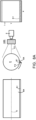
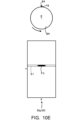
- FIG. 1A is a diagram schematically showing the schematic configuration of a defect detection apparatus according to an embodiment of the present disclosure, and is a front view of the defect detection apparatus as seen from the direction of the rotation axis of an object to be inspected.
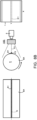
- FIG. 1B is a side view of the defect detection device viewed from the direction indicated by arrow A in FIG. 1A.
- FIG. 1C is a diagram for explaining a connected image generation process executed by the defect detector shown in FIG. 1A.
- FIG. 1D is a diagram showing an example of a connected image.
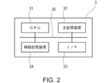
- FIG. 2 is a block diagram showing an example hardware configuration of a defect detector included in the defect detection apparatus.
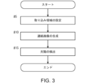
- FIG. 3 is a flow chart illustrating the processing performed by the defect detector.
- FIG. 1A is a diagram schematically showing the schematic configuration of a defect detection apparatus according to an embodiment of the present disclosure, and is a front view of the defect detection apparatus as seen from the direction of the rotation axis of an object to be inspected.
- FIG. 1B
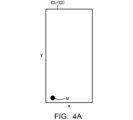
- FIG. 4A is a diagram schematically illustrating an example of a connected image generated when a simulated marker simulating a defect that is visualized when viewed from any direction is attached to an object to be inspected
- FIG. 1B is a diagram showing an example of a connected image CI 1 for a capture area TA 1 shown in FIG.
- FIG. 4B is a diagram showing an example of a connected image CI2 for the capture area TA2 shown in FIG. 1B.
- FIG. 4C is a diagram showing an example of a connected image CI3 for the capture area TA3 shown in FIG. 1B.
- FIG. 4D is a diagram showing an example of a connected image CI 4 for the capture area TA 4 shown in FIG. 1B.
- FIG. 1B is a diagram schematically illustrating an example of a connected image generated when a simulated marker simulating a defect that is visualized when viewed from any direction is attached to an object to be inspected
- FIG. 1B is a diagram showing an
- FIG. 4E is a diagram showing an example of a connected image CI 5 for the capture area TA 5 shown in FIG. 1B.
- FIG. 5A is a diagram schematically illustrating an example of a captured image generated when a defect that can be visualized when viewed from any direction exists on the surface of a cylindrical test object.
- FIG. 10 is a diagram showing a captured image I generated when F1 is positioned in capture area TA1 ;
- FIG. 5B is a diagram showing a captured image I generated when the defect F1 is located in the capture area TA3 .
- FIG. 5C is a diagram showing the captured image I generated when the defect F1 is located in the capture area TA5 .
- FIG. 6A is a diagram schematically illustrating an example of a captured image generated when a defect visible only when viewed from a specific direction exists on the surface of a cylindrical test object.
- FIG. 10 is a diagram showing a captured image I generated when F2 is positioned in capture area TA1 ;
- FIG. 6B is a diagram showing the captured image I generated when the defect F2 is located in the capture area TA3 .
- FIG. 6C is a diagram showing the captured image I generated when the defect F2 is located in the capture area TA5 .
- FIG. 7A is a diagram schematically illustrating an example of a connected image generated by rotating the inspection object having the same defect as that shown in FIG .
- FIG. 10 is a diagram showing a connected image CI 1 generated for .
- FIG. 7B is a diagram showing a connected image CI2 generated for the capture area TA2 .
- FIG. 7C shows a connected image CI3 generated for the capture area TA3 .
- FIG. 7D shows a connected image CI 4 generated for the capture area TA 4.
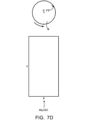
- FIG. 7E shows the connected image CI 5 generated for the capture area TA 5.
- FIG. 8A is a diagram schematically illustrating an example of a captured image generated for a substantially cylindrical inspected object having a convex portion, and is a captured image generated when the defect F3 is positioned in the capture area TA1 .
- FIG. 3 shows I.
- FIG. FIG. 8B is a diagram showing the captured image I when the defect F3 is located in the capture area TA3 .
- FIG. 8C is a diagram showing the captured image I when the defect F3 is located in the capture area TA5 .
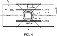
- FIG. 9 is a diagram for explaining capture areas set in the examples shown in FIGS. 8A to 8C.
- FIG. 10A is a diagram for schematically explaining an example of a connected image generated by rotating the inspection object having the same defect as that shown in FIG. 8A one round counterclockwise.
- FIG. 10 is a diagram showing a connected image CI 1 generated for .
- FIG. 10B is a diagram showing a connected image CI2 generated for the capture area TA2 .
- FIG. 10C shows a connected image CI3 generated for the capture area TA3 .
- FIG. 10D shows the connected image CI 4 generated for the capture area TA 4.
- FIG. 10E shows a connected image CI 5 generated for the capture area TA 5.
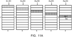
- FIG. 11A is a diagram schematically explaining a method of regenerating a connected image, and is a diagram showing a connected image CI before regeneration.
- FIG. 11B is a diagram showing the process of regenerating a connected image.
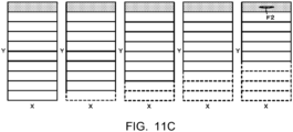
- FIG. 11C is a diagram showing a regenerated concatenated image.
- FIG. 12A is a diagram schematically illustrating an example of a captured image generated when a defect visible only when viewed from a specific direction exists on the surface of a cylindrical test object.
- FIG. 10 is a diagram showing a captured image I generated when F2 is positioned in capture area TA5 ;
- FIG. 12B is a diagram showing the captured image I when the defect F4 whose direction is different from that of the defect F2 is positioned in the capture area TA1 .
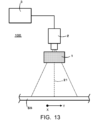
- FIG. 13 is a diagram schematically showing a state in which the defect detection apparatus according to the present embodiment is applied to a plate-shaped object to be inspected.
- a defect detection apparatus detects defects on the surface of an object to be inspected.
- the surface of the object to be inspected moves in a predetermined movement direction.
- the defect detection device includes an illuminator, a two-dimensional imaging device, and a defect detector.
- the illuminator irradiates the surface of the object to be inspected with light.
- a two-dimensional imaging machine has a visual axis in the normal direction of the surface of the object to be inspected.
- a two-dimensional imager receives light from a surface of an object to be inspected and generates a plurality of captured images having a two-dimensional area.
- the two-dimensional area is defined by a first axis in a direction corresponding to the moving direction, and a second axis in a direction corresponding to a direction orthogonal to the visual axis and the first axis.
- the defect detector detects defects on the surface of the object to be inspected based on the captured image.
- the defect detector is configured to perform the following processes. - A process of setting a plurality of capture areas arranged at different positions in the direction of the first axis in each of the captured images and extending in the direction of the second axis; ⁇ A plurality of connected images corresponding to a plurality of capture regions are generated by connecting the images included in each capture region of the captured images that are sequentially generated as the surface of the object to be inspected moves. and a process of detecting a pixel group corresponding to a defect from a plurality of connected images (first configuration)
- the two-dimensional imaging machine sequentially receives light over a two-dimensional area from the surface of the object to be inspected as the surface of the object to be inspected moves.
- the angle of view of the two-dimensional imaging device includes information captured from a plurality of different imaging directions.
- the defect detector first sets a plurality of capture areas in each captured image.
- the plurality of capture areas are arranged at different positions in the direction of the first axis, and each extend in the direction of the second axis (the axis in the direction corresponding to the direction orthogonal to the visual axis and the first axis).
- the plurality of capture areas are arranged at positions with different imaging directions in the direction corresponding to the movement direction of the surface of the object to be inspected.
- the defect detector corresponds to a plurality of capture areas by connecting images included in each capture area of captured images that are sequentially generated as the surface of the object to be inspected moves. Generate multiple concatenated images. As a result, one connected image is obtained by connecting the images included in the same captured area among the plurality of captured images. In other words, one connected image is obtained by connecting images captured from the same imaging direction among a plurality of captured images. Therefore, the plurality of connected images are images captured from different imaging directions, and include information when viewed from different imaging directions.
- the defect detector compares, for example, the density values of all pixels forming each connected image with a predetermined threshold to determine whether a pixel group corresponding to a defect exists in any of the plurality of connected images. It is possible to detect whether or not Therefore, according to the defect detection apparatus of the first configuration, even defects that are visible only when viewed from a specific direction can be detected.
- the object to be inspected is preferably a rotating body.
- the object to be inspected can be rotated around a predetermined rotation axis so that its circumferential direction is the moving direction of the surface of the object to be inspected.
- the two-dimensional imaging machine may sequentially generate a plurality of captured images as the object to be inspected rotates more than once (second configuration).
- Steel pipes, steel bars, wheels, axles, crankshafts, etc. can be exemplified as objects to be inspected that are rotating bodies.
- the object to be inspected is not limited to a rotating body, and may be, for example, a plate-like object such as a steel plate. If the object to be inspected is a plate-like object, the defect detection apparatus can also detect defects on the surface of the object to be inspected that moves (is transported) in its longitudinal direction.
- the illuminator irradiates the surface of the inspected object on which the magnetized fluorescent magnetic powder is scattered with ultraviolet light.
- the two-dimensional imaging device may receive light from the surface of the object to be inspected irradiated with ultraviolet light and generate a plurality of captured images (third configuration).
- the two-dimensional imaging device receives light emitted from the fluorescent magnetic particles adhering to the surface of the object to be inspected as the light from the surface of the object to be inspected.
- the defect detection device can be used for magnetic particle flaw detection.
- the defect detection device is not limited to magnetic particle flaw detection.
- the defect detection device emits visible light from the illuminator without scattering fluorescent magnetic powder on the surface of the object to be inspected, and the two-dimensional imaging machine emits light from the surface of the object to be inspected. It may be configured to receive reflected visible light.
- the defect detector generates a plurality of connected images such that the same part of the object to be inspected is displayed at the same position among the plurality of connected images (fourth configuration).
- the defect detection apparatus having the fourth configuration has the advantage of facilitating evaluation of the direction of the defect.
- the defect may be visualized only when viewed from a specific direction (fifth configuration).
- the defect detection device is not limited to this, and can be used to detect defects that are visualized when viewed from any of a plurality of different directions.
- a defect detection method detects defects on the surface of an object to be inspected.
- the surface of the object to be inspected moves in a predetermined moving direction.
- the defect detection method includes an illumination step, an imaging step, and a defect detection step.
- the illumination step the illuminator irradiates the surface of the object to be inspected with light.
- the imaging step a two-dimensional imaging machine having a visual axis in the direction normal to the surface of the object to be inspected sequentially receives light from the surface of the object to be inspected to generate a plurality of captured images having two-dimensional regions. .
- the two-dimensional area is defined by a first axis in a direction corresponding to the moving direction, and a second axis in a direction corresponding to a direction orthogonal to the visual axis and the first axis.
- the defect detector detects defects on the surface of the object to be inspected based on the captured image.
- the defect detection step includes a capture area setting step, a connected image generation step, and a detection step.
- the capturing area setting step a plurality of capturing areas arranged at different positions in the direction of the first axis and extending in the direction of the second axis are set in each captured image.
- the connected image generation step images included in each capture region of captured images sequentially generated along with movement of the surface of the object to be inspected are connected for each capture region to obtain a plurality of images corresponding to the plurality of capture regions. generates a concatenated image of
- a pixel group corresponding to a defect is detected from a plurality of connected images (sixth configuration).
- the two-dimensional imaging machine sequentially receives light over a two-dimensional area from the surface of the object to be inspected as the surface of the object to be inspected moves. Therefore, the angle of view of the two-dimensional imaging device includes information captured from a plurality of different imaging directions. Then, in the capturing area setting step, the defect detector first sets a plurality of capturing areas in each captured image.
- the plurality of capture areas are arranged at different positions in the direction of the first axis, and each extend in the direction of the second axis (the axis in the direction corresponding to the direction orthogonal to the visual axis and the first axis). In other words, the plurality of capture areas are arranged at positions with different imaging directions in the direction corresponding to the movement direction of the surface of the object to be inspected.
- the defect detector connects, for each captured image, images included in captured images sequentially generated as the surface of the object to be inspected moves. generates a plurality of concatenated images corresponding to the captured regions of .
- one connected image is obtained by connecting the images included in the same captured area among the plurality of captured images.
- one connected image is obtained by connecting images captured from the same imaging direction among a plurality of captured images. Therefore, the plurality of connected images are images captured from different imaging directions, and include information when viewed from different imaging directions.
- the defect detector compares the density values of all pixels constituting each connected image with a predetermined threshold value to determine whether a pixel corresponding to a defect is detected in one of the plurality of connected images. It is possible to detect whether groups exist or not. Therefore, according to the defect detection method of the sixth configuration, it is possible to detect even defects that are visible only when viewed from a specific direction.
- the object to be inspected is a rotating body that rotates about a predetermined rotation axis, and magnetic particle flaw detection is performed on the object to be inspected. Note that the present disclosure is not limited to magnetic particle flaw detection.
- FIG. 1A to 1D are diagrams schematically showing the schematic configuration of a defect detection device according to an embodiment of the present disclosure.
- FIG. 1A is a front view of the defect detection apparatus 100 viewed from the direction of the rotation axis C of the object S to be inspected.
- FIG. 1B is a side view of the defect detection apparatus 100 viewed from the direction indicated by arrow A in FIG. 1A.
- 1C and 1D are diagrams for explaining the process of generating a connected image executed by the defect detector 3 shown in FIG. 1A.
- illustration of the defect detector 3 is abbreviate
- FIG. 1B also shows the state of the capturing area setting process executed by the defect detector 3 .
- the defect detection apparatus 100 is an apparatus for detecting defects on the surface of an object S to be inspected.
- the subject S has a cylindrical shape.
- the object S to be inspected is a rotating body that rotates around the rotation axis C.
- the rotation axis C is the central axis of the object S to be inspected.
- the surface of the object S to be inspected moves in the circumferential direction of the object S to be inspected.
- the object S to be inspected is magnetized, and fluorescent magnetic powder is scattered on its surface.
- the defect detection apparatus 100 includes an illuminator 1 , a two-dimensional imaging device 2 and a defect detector 3 .
- the illuminator 1 is a device that irradiates the surface of the object S to be inspected with light.
- the illuminator 1 is arranged coaxially with the two-dimensional imaging device 2 and irradiates the surface of the object S to be inspected with ultraviolet light.
- a ring-type illumination device is used as the illumination device 1 .
- the illuminator 1 is arranged in a circular shape around the visual axis 21 of the two-dimensional imaging device 2 so as not to block the visual axis 21 of the two-dimensional imaging device 2 (the central axis of the imaging field of view 22 of the two-dimensional imaging device 2). are placed.
- the illuminator 1 includes, for example, multiple LED light sources that emit ultraviolet light.
- the illuminator 1 is configured to irradiate an area wider than the imaging field of view 22 of the two-dimensional imaging device 2 with ultraviolet light.
- a ring-shaped illuminator arranged coaxially with the two-dimensional imaging device 2 is used as the illuminator 1 .
- the illuminator 1 is not limited to this.
- various types of illuminators such as a line-type illuminator can be used.
- the illuminator 1 may irradiate the surface of the object S to be inspected with uniform light.
- the two-dimensional imaging device 2 has a visual axis 21 in the direction normal to the surface of the object S to be inspected, receives light from the surface of the object S to be inspected, and takes an image.
- the two-dimensional imaging device 2 captures an image by receiving light excited and emitted from fluorescent magnetic particles adhering to the surface of the object S to be inspected.
- the two-dimensional imaging device 2 generates a captured image I corresponding to the imaging visual field 22 by receiving light and capturing an image. As shown in FIG. 1C, the captured image I has a two-dimensional area.
- the two-dimensional area is defined by a first axis in a direction corresponding to the direction of movement of the surface of the object S to be inspected and a second axis in a direction corresponding to a direction orthogonal to the visual axis 21 and the first axis.
- the first axis is called the Y-axis
- the second axis is called the X-axis.
- the two-dimensional imaging device 2 for example, a monochrome or color area camera can be used.
- the area camera is composed of, for example, a 2048 ⁇ 2040 pixel CMOS or CCD.
- the two-dimensional imaging device 2 has an imaging field of view of 200 mm ⁇ 200 mm (resolution: 0.1 mm/pixel) when the distance to the object to be inspected S is 450 mm, for example, depending on the focal length and aperture of the lens used. Depth is set to 100 mm.
- the imaging field of view and the depth of field are not limited to these, and may be any suitable one depending on the type and surface properties of the object S to be inspected, the size of defects to be detected, the type of magnetic particles, etc. should be set to a value.
- the two-dimensional imaging machine 2 sequentially generates captured images I as the object S to be inspected rotates (rotates one round or more). That is, the two-dimensional imaging device 2 sequentially generates the captured images I as the surface of the object S to be inspected moves in the circumferential direction of the object S to be inspected.
- FIG. 1C shows an example in which n captured images I, that is, captured images I 1 to I n are generated.
- the defect detection apparatus 100 includes a rotation mechanism (not shown) that rotates the inspection object S around the rotation axis C. As shown in FIG.
- the two-dimensional imaging machine 2 can receive a rotation synchronization signal output from an encoder or the like included in the rotation mechanism.
- the two-dimensional imaging device 2 generates a captured image I each time the object S to be inspected rotates by a predetermined pitch (for example, 0.1 mm) in response to the rotation synchronization signal, and outputs the captured image I to the defect detector 3 .
- a predetermined pitch for example, 0.1 mm
- the defect detector 3 detects defects on the surface of the object S to be inspected based on the captured image I.
- the defect detector 3 is communicably connected to the two-dimensional imaging machine 2 .
- the defect detector 3 is, for example, a computer in which a program for executing various processes described later is installed.
- FIG. 2 is a block diagram showing an example of the hardware configuration of the defect detector 3.
- the defect detector 3 includes a CPU (Central Processing Unit) 31, a main storage device 32, an interface (I/F) 33, and an auxiliary storage device .
- the CPU 31 , main storage device 32 , interface 33 , and auxiliary storage device 34 are communicably connected to each other via a bus 35 .
- the main storage device 32 is a RAM (Random Access Memory) or the like that serves as a work area for the CPU 31 or the like.
- the interface 33 is connected to the two-dimensional imaging machine 2 (see FIGS. 1A and 1B) and a display (not shown).
- the auxiliary storage device 34 is an HDD (Hard Disk Drive) that stores various data, programs, and the like.
- the auxiliary storage device 34 may be a storage medium such as an SSD (Solid State Drive).
- the auxiliary storage device 34 stores a program for executing capture area setting processing, a program for executing connected image generation processing, and a program for executing defect detection processing.
- Various programs are loaded into the main storage device 32, the CPU 31 executes the programs, and the results are displayed on the display.
- FIG. 3 is a flow chart for explaining the processing executed by the defect detector 3. As shown in FIG. As shown in FIG. 3, the defect detector 3 performs a process (#5) for setting a capture area, a process (#10) for generating a connected image, and a process (#15) for detecting the presence or absence of a defect. configured to run.
- the defect detector 3 sets a plurality of capture areas TA corresponding to a plurality of positions defined in advance in the program in each captured image I (see FIG. 1B). ).
- the plurality of capturing areas TA are arranged at different positions in the Y-axis (first axis) direction and extend in the X-axis (second axis) direction.
- each capturing area TA has a size of 1 pixel in the Y-axis direction and 2048 pixels in the X-axis direction.
- five capture areas TA (TA 1 to TA 5 ) are set in each captured image I.
- each captured image I a plurality of capture areas TA (TA 1 to TA 5 ) are spaced apart in the Y-axis direction.
- the number and size of the capturing areas TA are not limited to the example of this embodiment, and can be set appropriately according to the direction of the defect to be detected.
- the defect detector 3 extracts (captures) the images included in the capture area TA of each captured image I, and connects them for each capture area TA.
- FIGS. 1C and 1D show, as an example, how the linking process is performed for the capture area TA3 .
- the two-dimensional imaging machine 2 sequentially generates captured images I 1 to I n as the object S to be inspected rotates one or more rounds.
- the defect detector 3 extracts an image included in the capture area TA 3 (TA 31 to TA 3n ) from each of the captured images I 1 to I n that are sequentially generated.
- the defect detector 3 Y Connect from the top to the bottom of the axis.
- the defect detector 3 also performs similar connection processing for the other capture areas TA 1 , TA 2 , TA 4 and TA 5 .
- the generation process of the captured image I by the two-dimensional imaging device 2 and the connection process of the image included in the capturing area TA of the captured image I by the defect detector 3 described above are performed when the object S to be inspected S rotates one or more times.
- a plurality of connected images CI corresponding to the plurality of capture areas TA are generated by repeating until the process is completed. That is, a connected image CI is generated for each capture area TA.
- FIG. 1D shows an example in which a connected image CI3 is generated for the capture area TA3 .
- the defect detector 3 After generating a plurality of connected images CI, the defect detector 3 executes processing for detecting defects from these connected images CI, as shown in step #15 of FIG. The defect detection process will be described below with reference to FIGS. 4A to 4E.
- FIGS. 4A to 4E show a connected image CI generated when a simulated marker M (see FIGS. 1A and 1B) simulating a defect visualized when viewed from any direction is attached to the inspected object S. It is a figure which illustrates typically the example of. Specifically, in FIGS. 4A to 4E , generation of the captured image I is started from the state shown in FIG .
- FIG. 1B is a diagram showing an example of a connected image CI generated by one rotation of the inspection object S counterclockwise in FIG. 1A. 4A shows an example of the connected image CI 1 for the capturing area TA 1 , FIG. 4B shows an example of the connected image CI 2 for the capturing area TA 2 , and FIG.
- 4C shows the connected image CI 3 for the capturing area TA 3.
- 4D shows an example of the connected image CI4 for the capturing area TA4
- FIG. 4E shows an example of the connected image CI5 for the capturing area TA5 .
- each of the connected images CI 1 to CI 5 is generated by connecting the images of the capturing area TA in the order in which they were extracted, so that the same part (simulated marker) of the subject S is generated.
- the position (position on the Y axis) of the site where M is attached differs among the connected images CI 1 to CI 5 .
- the defect detector 3 performs image processing on the generated multiple connected images CI, and detects pixel groups corresponding to defects from the multiple connected images CI. Specifically, for example, the defect detector 3 compares the density values (pixel values) of all pixels forming each connected image CI with a predetermined threshold value and binarizes them, thereby detecting defects. A group of pixels can be detected by distinguishing it from other groups of pixels. After performing the binarization process on each connected image CI, the defect detector 3 can perform noise removal such as removing a group of pixels having a small area (the number of pixels), if necessary.
- the defect detector 3 determines that a defect (flaw) exists in the object S to be inspected, and determines that the object S to be inspected S has a defect. may be displayed on the display device.
- the defect detector 3 can also cause the display to display the binarized connected image CI alone or together with the information indicating that the object S to be inspected has a defect.
- the inspector can visually check the connected image CI to confirm the defect.
- FIGS. 5A to 5C schematically illustrate an example of a captured image I generated when a defect F1 visible from any direction exists on the surface of a cylindrical inspection object S. It is a figure to do.
- the defect F1 is open on the surface of the object S to be inspected, and extends along the radial direction of the object S to be inspected in the depth direction.
- 5A shows a captured image I generated when the defect F1 is located in the capture area TA 1 (see FIG. 1B)
- FIG. 5B is a captured image I generated when the defect F1 is located in the capture area TA 3 (see FIG. 1B).
- FIG. 5C shows the captured image I when the defect F1 is located in the capturing area TA 5 (see FIG. 1B).
- the left figure is a side view of the inspected object S
- the middle figure is a front view of the inspected object S and the defect detection apparatus 100
- the right figure shows the captured image I.
- FIG. 1B the left figure is a side view
- FIGS. 5A to 5C As shown in FIGS. 5A to 5C, as the inspection object S rotates (counterclockwise rotation), the position of the defect F1 shifts from the position of the capture area TA1 (FIG. 5A) to the position of the capture area TA3. (FIG. 5B) to the location of the acquisition area TA 5 (FIG. 5C). Then, a captured image I in which the defect F1 is visualized is generated at each position.
- the defect F1 when the defect F1 is located in the capture area TA3 , the defect F1 is located on the visual axis 21 of the two-dimensional imaging machine 2. As shown in FIG. At this time, a captured image I is generated in which the pixel group corresponding to the defect F1 has the same shape and size as the actual object (actual magnetic particle pattern attracted to the defect F1). In contrast, when defect F1 is located in capture area TA1 , as shown in FIG. 5A, or when defect F1 is located in capture area TA5 , as shown in FIG. It is located away from the visual axis 21 of the imaging device 2 .
- the defect F1 since the defect F1 is imaged obliquely, the pixel group corresponding to the defect F1 becomes smaller in size than the actual object, the shape changes, and the resolution may become low. This change is remarkable if the angle of view of the two-dimensional imaging device 2 is large.
- FIGS. 6A to 6C schematically illustrate an example of a captured image I generated when a defect F2 visible only when viewed from a specific direction exists on the surface of a cylindrical inspection object S. It is a figure to do.
- FIG. 6A shows a captured image I generated when the defect F2 is located in the capture area TA 1 (see FIG. 1B)
- FIG. 6B is a captured image I generated when the defect F2 is located in the capture area TA 3 (see FIG. 1B).
- FIG. 6C shows the captured image I when the defect F2 is located in the capturing area TA 5 (see FIG. 1B).
- the left figure is a side view of the inspected object S
- the middle figure is a front view of the inspected object S and the defect detection apparatus 100
- the right figure shows the captured image I.
- FIG. in the right figures of FIGS. 6A and 6B, the position of the defect F2, which is not actually visualized but is supposed to be visualized, is indicated by a dotted line.
- the position of the defect F2 shifts from the position of the capture area TA1 (FIG. 6A) to the position of the capture area TA3. (FIG. 6B) to the location of the acquisition area TA 5 (FIG. 6C).
- the defect F2 is opened on the surface of the object S to be inspected, the depth direction is inclined from the radial direction of the object S to be inspected, and the depth direction extends along the surface of the object S to be inspected. Therefore, as shown in FIG.
- the imaging direction of the defect F2 is close to the depth direction of the defect F2, and the captured image I in which the defect F2 is visualized is generated.
- the angular difference between the imaging direction of the defect F2 and the depth direction of the defect F2 increases, and the defect F2 A captured image I in which is invisible is generated.
- any of the generated captured images I It is considered that the defect F2 is visualized in 1. Therefore, it is conceivable to adopt a method of detecting a pixel group corresponding to the defect F2 by performing image processing such as binarization on all of the plurality of captured images I. The same is true for defect F1 shown in FIGS. 5A to 5C.
- the defect detector 3 detects the image included in the capture area TA of each captured image I for each capture area TA.
- a configuration is adopted in which a plurality of connected images CI corresponding to a plurality of capturing areas TA are generated by connecting them.
- FIGS. 7A to 7E schematically illustrate an example of a connected image CI generated by rotating the inspected object S having the same defect F2 as shown in FIGS. 6A to 6C one round counterclockwise. It is a figure to do.
- the upper diagram shows the state where the defect F2 is located in the capture area TA1
- the lower diagram shows the connected image CI1 generated for the capture area TA1
- the upper diagram shows the state where the defect F2 is located in the capture area TA2
- the lower diagram shows the connected image CI2 generated for the capture area TA2 .
- the upper diagram shows the state where the defect F2 is located in the capture area TA3
- the lower diagram shows the connected image CI3 generated for the capture area TA3
- the upper diagram shows the state where the defect F2 is located in the capture area TA4
- the lower diagram shows the connected image CI4 generated for the capture area TA4
- the upper diagram shows the state where the defect F2 is located in the capture area TA5
- the lower diagram shows the connected image CI5 generated for the capture area TA5 .
- the defect F2 is not visualized in any of the connected images CI 1 to CI 4 respectively generated for the capture areas TA 1 to TA 4 .
- the defect F2 is visualized in the connected image CI5 generated for the capture area TA5 . Therefore, the defect detector 3 performs image processing on the plurality of generated connected images CI 1 to CI 5 , and among the plurality of connected images CI 1 to CI 5 , the pixel corresponding to the defect F2 is detected in the connected image CI 5. It is possible to detect the presence of groups.
- the resolution resolution in the Y-axis direction
- the imaging direction imaging direction in the Y-axis direction
- the binarization threshold value and the reference number of pixels for noise removal are the same in one connected image CI, the pixel group corresponding to the defect F2 can be detected with high accuracy.
- the defect F2 shown in FIGS. 6A to 6C was visible only when viewed from a specific direction due to the depth direction of the defect F2, but due to the shape of the object to be inspected, It is also possible that the defect is only visible when viewed from a particular direction.
- FIGS. 8A to 8C are diagrams for schematically explaining an example of the captured image I generated for the substantially cylindrical inspection subject SA having the convex portion S1.
- FIG. 9 is a diagram for explaining the capturing area TA set in the examples shown in FIGS. 8A to 8C.
- FIGS. 8A to 8C the defect F3 exists on one side surface of the convex portion S1.
- FIG. 8A shows a captured image I generated when defect F3 is located in capture area TA 1 (see FIG. 9).
- FIG. 8B shows the captured image I when the defect F3 is located in the capture area TA 3 (see FIG. 9).
- FIG. 8C shows the captured image I when the defect F3 is located in the capturing area TA 5 (see FIG. 9).
- the left figure is a side view of the inspection object SA
- the middle figure is a front view of the inspection object SA and the defect detection apparatus 100
- the right figure shows the captured image I.
- FIG. In the right diagrams of FIGS. 8A to 8C dotted lines indicate the positions of the protrusions S1 that are assumed to be visualized, although they are not actually visualized.
- the position of the defect F3 shifts from the position of the capture area TA1 (FIG. 8A) to the position of the capture area TA3. (FIG. 8B) to the position of the capture area TA 5 (FIG. 8C).
- the defect F3 is located on the side surface of the convex portion S1 on the opposite side (left side) to the side facing the two-dimensional imaging machine 2, so it is not visualized. Further, as shown in FIG.
- the side surfaces of the convex portion S1 are positioned above and below, and the defect F3 is positioned on the side surface of the lower convex portion S1, so that it is not visualized.
- the defect F3 is located on the side surface of the convex portion S1 on the side facing the two-dimensional imaging machine 2 (right side), and therefore is visualized.
- FIGS. 10A to 10E schematically illustrate an example of a connected image CI generated by rotating the object SA having the same defect F3 as shown in FIGS. 8A to 8C counterclockwise one round. It is a figure to do.
- the upper diagram shows the state where the defect F3 is located in the capture area TA1
- the lower diagram shows the connected image CI1 generated for the capture area TA1
- the upper diagram shows the state where the defect F3 is located in the capture area TA2
- the lower diagram shows the connected image CI2 generated for the capture area TA2 .
- the upper diagram shows the state where the defect F3 is located in the capture area TA3
- the lower diagram shows the connected image CI3 generated for the capture area TA3
- the upper diagram shows the state where the defect F3 is located in the capture area TA4
- the lower diagram shows the connected image CI4 generated for the capture area TA4
- the upper diagram shows the state where the defect F3 is located in the capture area TA5
- the lower diagram shows the connected image CI5 generated for the capture area TA5 .
- the position of the convex portion S1 which is not actually visualized but is assumed to be visualized, is indicated by a dotted line.
- the defect F3 is not visualized in any of the connected images CI 1 to CI 4 respectively generated for the capturing areas TA 1 to TA 4 .
- the defect F3 is visualized in the connected image CI5 generated for the capture area TA5 . Therefore, the defect detector 3 performs image processing on the plurality of generated connected images CI 1 to CI 5 , and among the plurality of connected images CI 1 to CI 5 , the pixel corresponding to the defect F3 is detected in the connected image CI 5. It is possible to detect the presence of groups.
- the convex portion S1) of the object to be inspected SA is not displayed at the same position (the same position in the Y-axis direction) among the connected images CI (CI 1 to CI 5 ).
- the display position in each connected image CI is shifted in the Y-axis direction from the display positions in other connected images CI with respect to the same part of the object to be inspected.
- the images included in each captured area TA of the captured image I sequentially generated by the two-dimensional imaging device 2 are arranged in the order of extraction (the order in which the captured image I was generated) from the top to the bottom of the Y axis. This is because the connected image CI is generated by combining the images.
- the same part of the subject to be inspected may be the same among the plurality of concatenated images CI. (the same position in the Y-axis direction) to regenerate the connected image CI.
- FIGS. 11A to 11C are diagrams schematically explaining a method for regenerating the connected image CI. Specifically, FIGS. 11A to 11C are diagrams explaining a method of regenerating the connected image CI shown in FIGS. 7A to 7E.
- FIG. 11A is a view showing the concatenated image CI before regeneration (a view corresponding to the concatenated image CI shown in FIGS. 7A to 7E). 2) represents the part where the defect F2 exists.
- FIG. 11A shows how each connected image CI starts to be generated based on the state where the defect F2 is located in the capture area TA1 . The image is located at the top of the Y-axis.
- images corresponding to the portion where the defect F2 exists are displayed according to the amount of positional deviation (the amount of positional deviation in the Y-axis direction) of the capture areas TA 2 to TA 5 with respect to the capture area TA 1 . It will be shifted downward in the direction of the Y-axis.
- the amount of positional deviation of the images corresponding to the same part of the subject S is determined by the position of each capturing area TA set in the captured image I and the pitch (for example, 0.1 mm) for generating the captured image I. ) and can be obtained by Therefore, as shown in FIG. 11B, images (images indicated by dashed lines in FIG. 11B) corresponding to the positional deviation amounts of the images corresponding to the same part of the subject S in the connected images CI 2 to CI 5 are shown in FIG. Move downward in the direction of the Y-axis, as shown at 11C. As a result, it is possible to regenerate the connected image CI in which the image corresponding to the same part of the subject S is displayed at the same position (the same position in the Y-axis direction) among the plurality of connected images CI. be possible.
- the defect detection apparatus 100 of this embodiment has an advantage that it is easy to evaluate the direction of the defect F2.
- FIG. 12A and 12B are diagrams for schematically explaining an example of a captured image I generated when a defect visible only when viewed from a specific direction exists on the surface of a cylindrical inspection object S. is.
- FIG. 12A shows a captured image I produced when the same defect F2 shown in FIGS. 6A-6C is located in capture area TA 5 (see FIG. 1B).
- FIG. 12B shows the captured image I when the defect F4 whose direction is different from that of the defect F2 is located in the capturing area TA 1 (see FIG. 1B).
- the left figure is a side view of the inspected object S
- the middle figure is a front view of the inspected object S and the defect detection apparatus 100
- the right figure shows the captured image I.
- FIG. 12A shows a captured image I produced when the same defect F2 shown in FIGS. 6A-6C is located in capture area TA 5 (see FIG. 1B).
- FIG. 12B shows the captured image I when the defect F4 whose direction is different from that
- both the defect F2 and the defect F4 are defects that open on the surface of the object S to be inspected and extend along the surface of the object S to be inspected in the depth direction.
- the depth direction from the opening extends in the rotation direction (counterclockwise) of the object S to be inspected
- the depth direction from the opening of the defect F4 is opposite to the rotation direction of the object S to be inspected. extending in the direction That is, the directions of both defects F2 and F4 are different.
- Defect F2 shown in FIG. 12A is visible when located in uptake area TA5 . That is, the defect F2 is visible in the concatenated image CI5 .
- defect F4 shown in FIG. 12B is visible when located in capture area TA1 . That is, defect F4 is visualized in concatenated image CI1 .
- the regenerated connected images CI 1 and CI 5 are displayed as the connected images CI 1 and CI 5 , and the same position in the Y-axis direction is displayed between the connected images CI 1 and CI 5 .
- the object to be inspected is a rotating body that rotates about the predetermined rotation axis C
- the object to be inspected is not limited to a rotating body.
- FIG. 13 is a diagram schematically showing a state in which the defect detection apparatus 100 according to the present embodiment is applied to a plate-shaped object to be inspected SB.
- the defect detection apparatus 100 can also be applied when a plate-like object such as a steel plate moving (conveyed) in the longitudinal direction is the object to be inspected SB.
- the longitudinal direction is the movement direction of the surface of the object SB to be inspected.
- the imaging device 2 may sequentially generate the captured image I having a two-dimensional area.
- the two-dimensional area has a first axis (Y-axis) in a direction corresponding to the movement direction of the surface of the object to be inspected SB and a second axis in a direction perpendicular to the visual axis 21 and the Y-axis of the two-dimensional imaging device 2 .
- 2 axes (X-axis).
- the multiple capture areas TA are arranged at different positions in the Y-axis direction and extend in the X-axis direction. Further, the defect detector 3 connects the images included in the capture areas TA of the picked-up images I sequentially generated along with the movement of the object to be inspected SB for each capture area TA, thereby forming a plurality of capture areas TA. Generate a corresponding plurality of concatenated images CI. By using this connected image CI, it is possible to detect even defects that are visible only when viewed from a specific direction, as in the case of the body of revolution.
- the present disclosure is not limited to this, and without scattering fluorescent magnetic powder on the surface of the object to be inspected, the illuminator 1 irradiates visible light, and the two-dimensional imaging device 2 emits The light may be visible light reflected by the surface of the object to be inspected.
- Illuminator 2 Two-dimensional imaging device 21: Visual axis 3: Defect detector 100: Defect detector CI: Connected image S, SA, SB: Object to be inspected TA: Capture area I: Captured image
Abstract
欠陥検出装置は、被検査体の表面に光を照射する照明機と、被検査体の表面の法線方向に視軸を有し、被検査体の表面の移動方向に対応する方向の第1軸と、視軸及び第1軸に直交する方向に対応する方向の第2軸とで規定される2次元領域を有する、複数の撮像画像を生成する2次元撮像機と、撮像画像に基づいて、被検査体の表面の欠陥を検出する欠陥検出機と、を備える。欠陥検出機は、撮像画像の各々において、第1軸の方向で互いに異なる位置に配置され、それぞれ第2軸の方向に延びる複数の取り込み領域を設定する処理(#5)と、被検査体の表面の移動に伴って逐次生成される撮像画像の各々の取り込み領域に含まれる画像を、取り込み領域毎に連結することで、複数の取り込み領域に対応する複数の連結画像を生成する処理(#10)と、複数の連結画像から欠陥に対応する画素群を検出する処理(#15)と、を実行する。
Description
本開示は、被検査体の、所定の移動方向に移動する表面の欠陥を検出する欠陥検出装置及び欠陥検出方法に関する。
磁粉を用いて被検査体の表面の検査を行う磁粉探傷では、磁化された被検査体の表面に、磁粉を含む磁粉液を塗布する。被検査体が磁化されていることにより、被検査体の表面に存在する開口又は未開口の欠陥から磁束が漏洩し、磁粉液に含まれる磁粉が欠陥に吸着される。磁粉が蛍光磁粉である場合には、被検査体に紫外光を照射することで磁粉が励起発光し、磁粉模様として可視化される。
検査員は、暗室内で磁粉模様を目視観察し、欠陥に起因した磁粉模様(欠陥模様)と、欠陥以外の表面粗さ等に起因した磁粉液の液溜まり等による磁粉模様(疑似模様)とを見分けながら、検査を行っている。しかしながら、検査の精度は検査員の技量に負う部分が大きく、発生する欠陥の形状や方向が多岐にわたり、欠陥模様が疑似模様と酷似している場合があることから、磁粉模様が欠陥模様であるか否かの見極めが難しい。また、検査作業は暗室内で長時間行われることや、特に形状が複雑な被検査体の場合には作業が更に難しくなることから、磁粉探傷の自動化が求められている。
磁粉探傷では、磁粉液が塗布された被検査体の表面に一様な光(蛍光磁粉の場合には紫外光)を照射し、作業員が磁粉模様を目視観察したり、作業員が撮像装置で撮像した磁粉模様の撮像画像を目視観察したりすることで、欠陥を検出する。また、撮像画像を画像処理することで、欠陥を自動検出することもできる。
磁粉探傷における被検査体の撮像方法については、数々の手法が提案されている。例えば、特許文献1には、鋼管のネジ部を磁粉探傷する磁粉探傷装置が提案されている。特許文献1に記載の磁粉探傷装置は、複数の2次元の撮像装置を鋼管の軸方向に並設し、鋼管を周方向に回転させながら、ネジ部全体の合成画像を生成する構成である。具体的には、特許文献1に記載の磁粉探傷装置では、各撮像装置によって取得した撮像画像から、鋼管の軸方向に対する各撮像装置の画角(角度φ1)のうち、ネジ部のネジ山の側面を撮像可能な角度φ2に相当する撮像端部領域のみを抽出すると共に、鋼管の周方向の微小角度Δθに相当する中心領域を切り出し、これらを繋ぎ合わせて、ネジ部全体の合成画像を生成し、この合成画像を用いて磁粉探傷を行っている(特許文献1の請求項1、請求項2、図3、及び図4等)。
しかしながら、本発明者らの知見によれば、欠陥には、その形状や方向に応じて、特定の方向から見たときにのみ可視化される(磁粉模様を観察できる)ものが存在する。特許文献1に記載の磁粉探傷装置では、一定の方向(角度φ2、及び角度Δθ内の方向)から撮像した磁粉模様のみを用いることになる。このため、特定の方向から見たときにのみ可視化される欠陥も検出対象とする場合、上記の一定の方向が上記の特定の方向と異なるときに、当該欠陥を検出できないという問題がある。
なお、上記の問題は、必ずしも磁粉探傷装置に限るものではなく、被検査体の表面に光を照射する照明機と、被検査体の表面からの光を受光して撮像画像を生成する撮像機と、を備える欠陥検出装置に共通する課題である。
本開示は、上記のような従来技術の問題を解決するためになされたものである。本開示の課題は、特定の方向から見たときにのみ可視化される欠陥であっても検出可能な欠陥検出装置及び欠陥検出方法を提供することである。
本開示に係る欠陥検出装置は、被検査体の表面の欠陥を検出する。被検査体の表面は、所定の移動方向に移動する。欠陥検出装置は、照明機と、2次元撮像機と、欠陥検出機と、を備える。照明機は、被検査体の表面に光を照射する。2次元撮像機は、被検査体の表面の法線方向に視軸を有する。2次元撮像機は、被検査体の表面からの光を受光して、2次元領域を有する複数の撮像画像を生成する。2次元領域は、上記移動方向に対応する方向の第1軸と、視軸及び第1軸に直交する方向に対応する方向の第2軸とで規定される。欠陥検出機は、撮像画像に基づいて、被検査体の表面の欠陥を検出する。欠陥検出機は、以下の処理を実行するように構成される。
・撮像画像の各々において、第1軸の方向で互いに異なる位置に配置され、それぞれ第2軸の方向に延びる複数の取り込み領域を設定する処理;
・被検査体の表面の移動に伴って逐次生成される撮像画像の各々の取り込み領域に含まれる画像を、取り込み領域毎に連結することで、複数の取り込み領域に対応する複数の連結画像を生成する処理;及び
・複数の連結画像から欠陥に対応する画素群を検出する処理
・撮像画像の各々において、第1軸の方向で互いに異なる位置に配置され、それぞれ第2軸の方向に延びる複数の取り込み領域を設定する処理;
・被検査体の表面の移動に伴って逐次生成される撮像画像の各々の取り込み領域に含まれる画像を、取り込み領域毎に連結することで、複数の取り込み領域に対応する複数の連結画像を生成する処理;及び
・複数の連結画像から欠陥に対応する画素群を検出する処理
また、本開示に係る欠陥検出方法は、被検査体の表面の欠陥を検出する。被検査体の表面は、所定の移動方向に移動する。欠陥検出方法は、照明ステップと、撮像ステップと、欠陥検出ステップと、を備える。照明ステップでは、照明機が、被検査体の表面に光を照射する。撮像ステップでは、被検査体の表面の法線方向に視軸を有する2次元撮像機が、被検査体の表面からの光を逐次受光して、2次元領域を有する複数の撮像画像を生成する。2次元領域は、上記移動方向に対応する方向の第1軸と、視軸及び第1軸に直交する方向に対応する方向の第2軸とで規定される。欠陥検出ステップでは、欠陥検出機が、撮像画像に基づいて、被検査体の表面の欠陥を検出する。欠陥検出ステップは、取り込み領域設定ステップと、連結画像生成ステップと、検出ステップと、を備える。取り込み領域設定ステップでは、撮像画像の各々において、第1軸の方向で互いに異なる位置に配置され、それぞれ第2軸の方向に延びる複数の取り込み領域を設定する。連結画像生成ステップでは、被検査体の表面の移動に伴って逐次生成される撮像画像の各々の取り込み領域に含まれる画像を、取り込み領域毎に連結することで、複数の取り込み領域に対応する複数の連結画像を生成する。検出ステップでは、複数の連結画像から欠陥に対応する画素群を検出する。
本開示に係る欠陥検出装置及び欠陥検出方法によれば、特定の方向から見たときにのみ可視化される欠陥であっても検出可能である。
実施形態に係る欠陥検出装置は、被検査体の表面の欠陥を検出する。被検査体の表面は、所定の移動方向に移動する。欠陥検出装置は、照明機と、2次元撮像機と、欠陥検出機と、を備える。照明機は、被検査体の表面に光を照射する。2次元撮像機は、被検査体の表面の法線方向に視軸を有する。2次元撮像機は、被検査体の表面からの光を受光して、2次元領域を有する複数の撮像画像を生成する。2次元領域は、上記移動方向に対応する方向の第1軸と、視軸及び第1軸に直交する方向に対応する方向の第2軸とで規定される。欠陥検出機は、撮像画像に基づいて、被検査体の表面の欠陥を検出する。欠陥検出機は、以下の処理を実行するように構成される。
・撮像画像の各々において、第1軸の方向で互いに異なる位置に配置され、それぞれ第2軸の方向に延びる複数の取り込み領域を設定する処理;
・被検査体の表面の移動に伴って逐次生成される撮像画像の各々の取り込み領域に含まれる画像を、取り込み領域毎に連結することで、複数の取り込み領域に対応する複数の連結画像を生成する処理;及び
・複数の連結画像から欠陥に対応する画素群を検出する処理(第1の構成)
・撮像画像の各々において、第1軸の方向で互いに異なる位置に配置され、それぞれ第2軸の方向に延びる複数の取り込み領域を設定する処理;
・被検査体の表面の移動に伴って逐次生成される撮像画像の各々の取り込み領域に含まれる画像を、取り込み領域毎に連結することで、複数の取り込み領域に対応する複数の連結画像を生成する処理;及び
・複数の連結画像から欠陥に対応する画素群を検出する処理(第1の構成)
第1の構成の欠陥検出装置によれば、2次元撮像機が、被検査体の表面の移動に伴って、逐次、被検査体の表面からの2次元領域に亘る光を受光して複数の撮像画像を生成するため、2次元撮像機の画角内には、複数の異なる撮像方向から撮像された情報が含まれることになる。そして、欠陥検出機は、まず、撮像画像の各々において、複数の取り込み領域を設定する。複数の取り込み領域は、第1軸の方向で互いに異なる位置に配置され、それぞれ第2軸(視軸及び第1軸に直交する方向に対応する方向の軸)の方向に延びている。換言すれば、複数の取り込み領域は、被検査体の表面の移動方向に対応する方向で撮像方向が互いに異なる位置に配置されている。
さらに、欠陥検出機は、被検査体の表面の移動に伴って逐次生成される撮像画像の各々の取り込み領域に含まれる画像を、取り込み領域毎に連結することで、複数の取り込み領域に対応する複数の連結画像を生成する。これにより、一つの連結画像は、複数の撮像画像間で同じ取り込み領域に含まれる画像が連結されたものとなる。換言すれば、一つの連結画像は、複数の撮像画像間で同じ撮像方向から撮像された画像が連結されたものとなる。このため、複数の連結画像は、互いに異なる撮像方向から撮像された画像となり、互いに異なる撮像方向から見たときの情報を含む画像となる。
したがって、特定の方向から見たときにのみ可視化される欠陥であっても、複数の連結画像のいずれか(いずれかの撮像方向から撮像された連結画像)においては、その欠陥が可視化された状態になることが期待できる。すなわち、連結画像において、欠陥に対応する画素群の濃度値(画素値)が他の画素の濃度値と異なる状態になることにより、欠陥が可視化されて識別可能になると期待される。このため、欠陥検出機は、例えば、各連結画像を構成する全画素の濃度値を所定のしきい値と比較することにより、複数の連結画像のいずれかに欠陥に対応する画素群が存在するか否かを検出することができる。よって、第1の構成の欠陥検出装置によれば、特定の方向から見たときにのみ可視化される欠陥であっても検出可能である。
上記欠陥検出装置において、好ましくは、被検査体は、回転体である。被検査体は、その周方向が被検査体の表面の移動方向となるように所定の回転軸を中心として回転することができる。この場合、2次元撮像機は、被検査体の1周以上の回転に伴って逐次複数の撮像画像を生成してもよい(第2の構成)。
回転体である被検査体としては、鋼管、棒鋼、車輪、車軸、クランクシャフト等を例示できる。
ただし、被検査体は、回転体に限られるものではなく、例えば、鋼板等の板状体であってもよい。被検査体が板状体である場合、欠陥検出装置は、その長手方向に移動する(搬送される)被検査体の表面の欠陥を検出することもできる。
上記欠陥検出装置において、好ましくは、照明機は、磁化され蛍光磁粉が散布された被検査体の表面に紫外光を照射する。この場合、2次元撮像機は、紫外光が照射された被検査体の表面からの光を受光して、複数の撮像画像を生成してもよい(第3の構成)。
第3の構成では、2次元撮像機は、被検査体の表面からの光として、被検査体の表面に付着した蛍光磁粉から励起発光された光を受光することになる。この場合、欠陥検出装置を磁粉探傷に用いることができる。
ただし、欠陥検出装置の用途は、磁粉探傷に限定されない。欠陥検出装置は、被検査体の表面に蛍光磁粉を散布することなく、照明機が可視光を照射し、2次元撮像機が、被検査体の表面からの光として、被検査体の表面で反射した可視光を受光するように構成されていてもよい。
上記欠陥検出装置において、好ましくは、欠陥検出機は、被検査体の同一の部位が、複数の連結画像の間で同一の位置に表示されるように、複数の連結画像を生成する(第4の構成)。
第4の構成では、被検査体の同一の部位が、複数の連結画像の間で同一の位置に表示される。このため、例えば、複数の連結画像を表示して検査員が目視した場合に、同一の部位に存在する欠陥が、複数の連結画像のうちのいずれの連結画像で可視化されているか(換言すれば、いずれの撮像方向から撮像された場合に可視化されているか)を把握し易くなる。このため、第4の構成の欠陥検出装置は、欠陥の方向を評価し易いという利点を有する。
上記欠陥検出装置において、欠陥は、特定の方向から見たときにのみ可視化されるものであってもよい(第5の構成)。
ただし、上記欠陥検出装置は、これに限るものではなく、複数の異なる方向のうち、いずれの方向から見たときにも可視化される欠陥を検出するのに用いることも可能である。
実施形態に係る欠陥検出方法は、被検査体の表面の欠陥を検出する。被検査体の表面は、所定の移動方向に移動する。欠陥検出方法は、照明ステップと、撮像ステップと、欠陥検出ステップと、を備える。照明ステップでは、照明機が、被検査体の表面に光を照射する。撮像ステップでは、被検査体の表面の法線方向に視軸を有する2次元撮像機が、被検査体の表面からの光を逐次受光して、2次元領域を有する複数の撮像画像を生成する。2次元領域は、上記移動方向に対応する方向の第1軸と、視軸及び第1軸に直交する方向に対応する方向の第2軸とで規定される。欠陥検出ステップでは、欠陥検出機が、撮像画像に基づいて、被検査体の表面の欠陥を検出する。欠陥検出ステップは、取り込み領域設定ステップと、連結画像生成ステップと、検出ステップと、を備える。取り込み領域設定ステップでは、撮像画像の各々において、第1軸の方向で互いに異なる位置に配置され、それぞれ第2軸の方向に延びる複数の取り込み領域を設定する。連結画像生成ステップでは、被検査体の表面の移動に伴って逐次生成される撮像画像の各々の取り込み領域に含まれる画像を、取り込み領域毎に連結することで、複数の取り込み領域に対応する複数の連結画像を生成する。検出ステップでは、複数の連結画像から欠陥に対応する画素群を検出する(第6の構成)。
第6の構成の欠陥検出方法によれば、撮像ステップにおいて、2次元撮像機が、被検査体の表面の移動に伴って、逐次、被検査体の表面からの2次元領域に亘る光を受光して複数の撮像画像を生成するため、2次元撮像機の画角内には、複数の異なる撮像方向から撮像された情報が含まれることになる。そして、取り込み領域設定ステップでは、欠陥検出機は、まず、撮像画像の各々において、複数の取り込み領域を設定する。複数の取り込み領域は、第1軸の方向で互いに異なる位置に配置され、それぞれ第2軸(視軸及び第1軸に直交する方向に対応する方向の軸)の方向に延びている。換言すれば、複数の取り込み領域は、被検査体の表面の移動方向に対応する方向で撮像方向が互いに異なる位置に配置されている。
さらに、連結画像生成ステップでは、欠陥検出機は、被検査体の表面の移動に伴って逐次生成される撮像画像の各々の取り込み領域に含まれる画像を、取り込み領域毎に連結することで、複数の取り込み領域に対応する複数の連結画像を生成する。これにより、一つの連結画像は、複数の撮像画像間で同じ取り込み領域に含まれる画像が連結されたものとなる。換言すれば、一つの連結画像は、複数の撮像画像間で同じ撮像方向から撮像された画像が連結されたものとなる。このため、複数の連結画像は、互いに異なる撮像方向から撮像された画像となり、互いに異なる撮像方向から見たときの情報を含む画像となる。
したがって、特定の方向から見たときにのみ可視化される欠陥であっても、複数の連結画像のいずれか(いずれかの撮像方向から撮像された連結画像)においては、その欠陥が可視化された状態になることが期待できる。すなわち、連結画像において、欠陥に対応する画素群の濃度値(画素値)が他の画素の濃度値と異なる状態になることにより、欠陥が可視化されて識別可能になると期待される。このため、検出ステップでは、欠陥検出機は、例えば、各連結画像を構成する全画素の濃度値を所定のしきい値と比較することにより、複数の連結画像のいずれかに欠陥に対応する画素群が存在するか否かを検出することができる。よって、第6の構成の欠陥検出方法によれば、特定の方向から見たときにのみ可視化される欠陥であっても検出可能である。
以下、本開示の実施形態について、添付図面を適宜参照しつつ説明する。各図において同一又は相当の構成については同一符号を付し、同じ説明を繰り返さない。以下に示す実施形態では、被検査体が所定の回転軸を中心として回転する回転体であり、被検査体に対して磁粉探傷を行う場合を例に挙げて説明する。なお、本開示は磁粉探傷に限定されるものではない。
図1A~図1Dは、本開示の一実施形態に係る欠陥検出装置の概略構成を模式的に示す図である。図1Aは、被検査体Sの回転軸Cの方向から見た欠陥検出装置100の正面図である。図1Bは、図1Aの矢符Aに示す方向から見た欠陥検出装置100の側面図である。図1C及び図1Dは、図1Aに示す欠陥検出機3が実行する連結画像の生成処理を説明する図である。なお、図1Bでは、欠陥検出機3の図示を省略している。また、図1Bには、欠陥検出機3が実行する取り込み領域の設定処理による様子も図示している。
図1A及び図1Bに示すように、本実施形態に係る欠陥検出装置100は、被検査体Sの表面の欠陥を検出する装置である。図1A及び図1Bに示す例において、被検査体Sは、円柱状を有する。被検査体Sは、回転軸Cを中心として回転する回転体である。回転軸Cは、被検査体Sの中心軸である。被検査体Sが回転軸Cを中心として回転することにより、被検査体Sの表面が被検査体Sの周方向に移動する。本実施形態では、被検査体Sは、磁化され、その表面に蛍光磁粉が散布されている。欠陥検出装置100は、照明機1と、2次元撮像機2と、欠陥検出機3と、を備える。
照明機1は、被検査体Sの表面に光を照射する装置である。照明機1は、2次元撮像機2と同軸上に配置され、被検査体Sの表面に紫外光を照射する。本実施形態では、照明機1として、リング型照明機が用いられている。照明機1は、2次元撮像機2の視軸21(2次元撮像機2の撮像視野22の中心軸)を塞がないように、2次元撮像機2の視軸21の周りに円形状に配置されている。照明機1は、例えば、紫外光を出射する複数のLED光源を含む。照明機1は、2次元撮像機2の撮像視野22よりも広い範囲に紫外光を照射するように構成されている。
本実施形態では、照明機1として、2次元撮像機2と同軸に配置されたリング型照明機が用いられている。ただし、照明機1は、これに限られるものではない。照明機1として、ライン型照明機等の種々の形態の照明機を用いることができる。照明機1は、被検査体Sの表面に一様な光を照射できるものであればよい。
2次元撮像機2は、被検査体Sの表面の法線方向に視軸21を有し、被検査体Sの表面からの光を受光して撮像する。本実施形態では、2次元撮像機2は、被検査体Sの表面に付着した蛍光磁粉から励起発光された光を受光して撮像する。2次元撮像機2は、光を受光して撮像することで、撮像視野22に対応する撮像画像Iを生成するものである。図1Cに示すように、撮像画像Iは、2次元領域を有する。2次元領域は、被検査体Sの表面の移動方向に対応する方向の第1軸と、視軸21及び第1軸に直交する方向に対応する方向の第2軸とで規定される。本実施形態では、第1軸をY軸と称し、第2軸をX軸と称する。
2次元撮像機2としては、例えば、モノクロ又はカラーのエリアカメラを用いることができる。エリアカメラは、例えば、2048画素×2040画素のCMOSやCCDから構成される。2次元撮像機2は、用いるレンズの焦点距離や絞りによって、例えば、被検査体Sまでの距離が450mmのときの撮像視野が200mm×200mm(分解能:0.1mm/画素)で、被写界深度が100mmに設定される。ただし、撮像視野及び被写界深度は、これに限定されるものではなく、被検査体Sの種類や表面性状、検出対象とする欠陥の寸法、磁粉の種類等に応じて、適切な任意の値に設定すればよい。
2次元撮像機2は、被検査体Sの回転(1周以上の回転)に伴って、撮像画像Iを逐次生成する。すなわち、2次元撮像機2は、被検査体Sの表面が被検査体Sの周方向に移動するのに伴って、撮像画像Iを逐次生成する。図1Cには、n枚の撮像画像I、すなわち撮像画像I1~Inが生成される例を図示している。具体的には、欠陥検出装置100は、回転軸Cを中心として被検査体Sを回転させる回転機構(図示略)を備える。2次元撮像機2は、回転機構が具備するエンコーダ等から出力される回転同期信号を受信することができる。2次元撮像機2は、回転同期信号に応じて、被検査体Sが所定のピッチ(例えば、0.1mm)回転する毎に撮像画像Iを生成し、欠陥検出機3に出力する。
欠陥検出機3は、撮像画像Iに基づいて、被検査体Sの表面の欠陥を検出する。欠陥検出機3は、2次元撮像機2と通信可能に接続されている。欠陥検出機3は、例えば、後述の各種の処理を実行するプログラムがインストールされたコンピュータである。
図2は、欠陥検出機3のハードウェア構成の一例を示すブロック図である。図2に示すように、欠陥検出機3は、CPU(Central Processing Unit)31と、主記憶装置32と、インタフェース(I/F)33と、補助記憶装置34と、を備える。CPU31、主記憶装置32、インタフェース33、及び補助記憶装置34は、バス35により互いに通信可能に接続されている。
主記憶装置32は、CPU31のワークエリア等になるRAM(Random Access Memory)等である。インタフェース33は、2次元撮像機2(図1A及び図1B参照)、及び表示機(図示略)に接続される。補助記憶装置34は、各種データやプログラム等が記憶されるHDD(Hard Disk Drive)である。補助記憶装置34は、SSD(Solid State Drive)等のような記憶媒体であってもよい。補助記憶装置34には、取り込み領域の設定処理を実行するプログラム、連結画像の生成処理を実行するプログラム、及び欠陥の検出処理を実行するプログラムが格納されている。各種のプログラムが主記憶装置32にロードされて、CPU31がプログラムを実行し、その結果が表示機に表示される。
以下、図1B、図1C、図1D、及び図3を参照して、欠陥検出機3による処理を詳細に説明する。図3は、欠陥検出機3が実行する処理を説明するフローチャートである。図3に示すように、欠陥検出機3は、取り込み領域を設定する処理(#5)と、連結画像を生成する処理(#10)と、欠陥の有無を検出する処理(#15)とを実行するように構成される。
まず、図3のステップ#5に示すように、欠陥検出機3は、各撮像画像Iにおいて、予めプログラム内で定義された複数の位置に対応する複数の取り込み領域TAを設定する(図1B参照)。複数の取り込み領域TAは、Y軸(第1軸)の方向で互いに異なる位置に配置され、それぞれX軸(第2軸)の方向に延びている。本実施形態では、取り込み領域TAのそれぞれが、Y軸の方向に1画素、及びX軸の方向に2048画素の大きさを有する。本実施形態では、撮像画像Iのそれぞれにおいて5つの取り込み領域TA(TA1~TA5)が設定されている。各撮像画像Iにおいて、複数の取り込み領域TA(TA1~TA5)は、Y軸の方向に間隔をあけて配置されている。ただし、取り込み領域TAの数及び大きさは、本実施形態の例に限定されるものではなく、検出対象とする欠陥の方向等に応じて、適宜設定することが可能である。
次に、図3のステップ#10に示すように、欠陥検出機3は、各撮像画像Iの取り込み領域TAに含まれる画像を抽出し(取り込み)、取り込み領域TA毎に連結する。図1C及び図1Dには、一例として、取り込み領域TA3についての連結処理の様子を図示している。図1Cに示すように、被検査体Sが1周以上回転するのに伴って、2次元撮像機2が撮像画像I1~Inを逐次生成する。欠陥検出機3は、逐次生成される撮像画像I1~Inの各々から取り込み領域TA3(TA31~TA3n)に含まれる画像を抽出する。欠陥検出機3は、図1Dに示すように、撮像画像I1~Inの各々から抽出された取り込み領域TA3の画像を、抽出された順に(撮像画像Iが生成された順に)、Y軸の上から下に向けて連結する。欠陥検出機3は、他の取り込み領域TA1、TA2、TA4、TA5についても、同様の連結処理を実行する。
以上に説明した、2次元撮像機2による撮像画像Iの生成処理と、欠陥検出機3による撮像画像Iの取り込み領域TAに含まれる画像の連結処理とが、被検査体Sが1周以上回転するまで繰り返されることで、複数の取り込み領域TAに対応する複数の連結画像CIが生成される。すなわち、取り込み領域TAの各々について連結画像CIが生成される。図1Dには、取り込み領域TA3について連結画像CI3が生成される例を示している。
欠陥検出機3は、複数の連結画像CIを生成した後、図3のステップ#15に示すように、これらの連結画像CIから欠陥を検出する処理を実行する。以下、欠陥の検出処理について、図4A~図4Eを参照して説明する。
図4A~図4Eは、いずれの方向から見たときにも可視化される欠陥を模擬した模擬マーカM(図1A及び図1B参照)を被検査体Sに取り付けた場合に生成される連結画像CIの例を模式的に説明する図である。具体的には、図4A~図4Eは、図1Bに示す状態(模擬マーカMが取り込み領域TA1と取り込み領域TA2との間に位置する状態)から撮像画像Iの生成を開始し、被検査体Sが図1Aの反時計回りに1周回転することで生成される連結画像CIの例を示す図である。図4Aは、取り込み領域TA1についての連結画像CI1の例を、図4Bは、取り込み領域TA2についての連結画像CI2の例を、図4Cは、取り込み領域TA3についての連結画像CI3の例を、図4Dは、取り込み領域TA4についての連結画像CI4の例を、図4Eは、取り込み領域TA5についての連結画像CI5の例をそれぞれ示す。
図4A~図4Eに示すように、各連結画像CI1~CI5は、取り込み領域TAの画像が、抽出された順に連結されて生成されるため、被検査体Sの同一の部位(模擬マーカMが取り付けられた部位)の位置(Y軸の位置)は、連結画像CI1~CI5の間で異なるものとなる。
図3のステップ#15に示すように、欠陥検出機3は、生成した複数の連結画像CIに対して画像処理を施し、複数の連結画像CIから欠陥に対応する画素群を検出する。具体的には、例えば、欠陥検出機3は、各連結画像CIを構成する全画素の濃度値(画素値)を所定のしきい値と比較して2値化することで、欠陥に対応する画素群を他の画素群と区別化して検出することができる。欠陥検出機3は、各連結画像CIに対して2値化処理を施した後、必要に応じ、小さな面積(画素数)の画素群を除去する等のノイズ除去を実行することができる。欠陥検出機3は、連結画像CIのいずれかに欠陥に対応する画素群が存在する場合、被検査体Sに欠陥(傷)が存在すると判定して、被検査体Sに欠陥が存在することを示す情報を表示機に表示させてもよい。欠陥検出機3は、被検査体Sに欠陥が存在することを示す情報と併せて、又は単独で2値化処理された連結画像CIを表示機に表示させることもできる。2値化処理された連結画像CIが表示機に表示された場合、検査員は、連結画像CIを目視して欠陥を確認することができる。
以下、本実施形態に係る欠陥検出装置100を用いることで、種々の被検査体及び欠陥について生成される撮像画像I及び連結画像CIの例について説明する。
図5A~図5Cは、円柱状の被検査体Sの表面に、いずれの方向から見たときにも可視化される欠陥F1が存在する場合に生成される撮像画像Iの例を模式的に説明する図である。欠陥F1は、被検査体Sの表面で開口し、深さ方向が被検査体Sの径方向に沿って延びている。図5Aは、欠陥F1が取り込み領域TA1(図1B参照)に位置するときに生成される撮像画像Iを、図5Bは、欠陥F1が取り込み領域TA3(図1B参照)に位置するときの撮像画像Iを、図5Cは、欠陥F1が取り込み領域TA5(図1B参照)に位置するときの撮像画像Iをそれぞれ示す。図5A~図5Cにおいて、左図は、被検査体Sの側面図であり、中央図は、被検査体S及び欠陥検出装置100の正面図であり、右図は、撮像画像Iを示す。
図5A~図5Cに示すように、被検査体Sの回転(反時計回りの回転)に伴い、欠陥F1の位置は、取り込み領域TA1の位置(図5A)から、取り込み領域TA3の位置(図5B)を経て、取り込み領域TA5の位置(図5C)に移動する。そして、それぞれの位置において、欠陥F1が可視化された撮像画像Iが生成される。
図5Bに示すように、欠陥F1が取り込み領域TA3に位置するとき、欠陥F1は、2次元撮像機2の視軸21上の位置にある。このときには、欠陥F1に対応する画素群が実物(欠陥F1に吸着した実際の磁粉模様)と同一の形状・寸法となった撮像画像Iが生成される。これに対して、図5Aに示すように、欠陥F1が取り込み領域TA1に位置するとき、又は図5Cに示すように、欠陥F1が取り込み領域TA5に位置するとき、欠陥F1は、2次元撮像機2の視軸21から離れた位置にある。このときには、欠陥F1を斜めから撮像することになるため、欠陥F1に対応する画素群が実物よりも小さな寸法となり、形状も変化してしまい、低分解能となる場合がある。2次元撮像機2の画角が大きければ、この変化は顕著である。
図6A~図6Cは、円柱状の被検査体Sの表面に、特定の方向から見たときにのみ可視化される欠陥F2が存在する場合に生成される撮像画像Iの例を模式的に説明する図である。図6Aは、欠陥F2が取り込み領域TA1(図1B参照)に位置するときに生成される撮像画像Iを、図6Bは、欠陥F2が取り込み領域TA3(図1B参照)に位置するときの撮像画像Iを、図6Cは、欠陥F2が取り込み領域TA5(図1B参照)に位置するときの撮像画像Iをそれぞれ示す。図6A~図6Cにおいて、左図は、被検査体Sの側面図であり、中央図は、被検査体S及び欠陥検出装置100の正面図であり、右図は、撮像画像Iを示す。なお、図6A及び図6Bの右図には、実際には可視化されないが、仮に可視化されると考えた場合の欠陥F2の位置を点線で図示している。
図6A~図6Cに示すように、被検査体Sの回転(反時計回りの回転)に伴い、欠陥F2の位置は、取り込み領域TA1の位置(図6A)から、取り込み領域TA3の位置(図6B)を経て、取り込み領域TA5の位置(図6C)に移動する。欠陥F2は、被検査体Sの表面で開口し、深さ方向が被検査体Sの径方向から傾き、深さ方向が被検査体Sの表面に沿うように延びている。このため、図6Cに示すように、取り込み領域TA5の位置では、欠陥F2の撮像方向が欠陥F2の深さ方向に近くなり、欠陥F2が可視化された撮像画像Iが生成される。これに対して、図6A及び図6Bに示すように、取り込み領域TA1や取り込み領域TA3の位置では、欠陥F2の撮像方向と欠陥F2の深さ方向との角度差が大きくなり、欠陥F2が不可視の撮像画像Iが生成される。
ここで、図6A~図6Cに示す例において、被検査体Sが短ピッチ(例えば、0.1mm)回転する毎に撮像画像Iを逐次生成すれば、生成された複数の撮像画像Iのいずれかにおいて、欠陥F2が可視化されると考えられる。このため、この複数の撮像画像Iの全てに対して、2値化等の画像処理を施すことで、欠陥F2に対応する画素群を検出する方法を採用することも考えられる。図5A~図5Cに示す欠陥F1についても同様である。
しかしながら、このような方法では、画像処理を施すべき撮像画像Iの数が多大になり、検出に時間を要するという問題がある。また、2次元撮像機2の画角が大きければ、1枚の撮像画像I内での画素の位置によって分解能の差が大きくなったり、1枚の撮像画像I内での撮像方向が大きく異なる。これらのことに起因して、1枚の撮像画像I内を同一のしきい値と比較して2値化したり、同一の画素数を基準としてノイズ除去を実行したのでは、欠陥に対応する画素群を精度良く検出できないおそれがある。さらに、特定の方向から見たときにのみ可視化される欠陥に対応するため、視軸21の方向が異なる複数の2次元撮像機2を配置することは、機械的な干渉の問題やコストの高騰を招き、現実的ではないという問題がある。
このような問題を解決するため、本実施形態に係る欠陥検出装置100では、前述のように、欠陥検出機3が、各撮像画像Iの取り込み領域TAに含まれる画像を、取り込み領域TA毎に連結することで、複数の取り込み領域TAに対応する複数の連結画像CIを生成する構成を採用している。
図7A~図7Eは、図6A~図6Cに示すものと同じ欠陥F2が存在する被検査体Sが反時計回りに1周回転することで生成される連結画像CIの例を模式的に説明する図である。図7Aにおいて、上図は、欠陥F2が取り込み領域TA1に位置する状態を、下図は、取り込み領域TA1について生成される連結画像CI1をそれぞれ示す。図7Bにおいて、上図は、欠陥F2が取り込み領域TA2に位置する状態を、下図は、取り込み領域TA2について生成される連結画像CI2をそれぞれ示す。図7Cにおいて、上図は、欠陥F2が取り込み領域TA3に位置する状態を、下図は、取り込み領域TA3について生成される連結画像CI3をそれぞれ示す。図7Dにおいて、上図は、欠陥F2が取り込み領域TA4に位置する状態を、下図は、取り込み領域TA4について生成される連結画像CI4をそれぞれ示す。図7Eにおいて、上図は、欠陥F2が取り込み領域TA5に位置する状態を、下図は、取り込み領域TA5について生成される連結画像CI5をそれぞれ示す。
図7A~図7Dに示すように、取り込み領域TA1~TA4についてそれぞれ生成される連結画像CI1~CI4では、いずれも欠陥F2が可視化されていない。これに対して、図7Eに示すように、取り込み領域TA5について生成される連結画像CI5では、欠陥F2が可視化されている。したがって、欠陥検出機3は、生成した複数の連結画像CI1~CI5に対して画像処理を施し、複数の連結画像CI1~CI5のうち、連結画像CI5に欠陥F2に対応する画素群が存在することを検出可能である。
なお、分解能(Y軸方向の分解能)及び撮像方向(Y軸方向についての撮像方向)は、連結画像CIの間では異なるものの、1枚の連結画像CI内では同等である。このため、2値化のしきい値や、ノイズ除去の基準画素数は、連結画像CIの間では異なるものを用いることが好ましい。ただし、2値化のしきい値や、ノイズ除去の基準画素数は、1枚の連結画像CI内で同一のものを用いても、欠陥F2に対応する画素群を精度良く検出可能である。
図6A~図6Cに示す欠陥F2は、欠陥F2の深さ方向に起因して、特定の方向から見たときにのみ可視化されるものであったが、被検査体の形状に起因して、欠陥が特定の方向から見たときにのみ可視化されることも考えられる。
図8A~図8Cは、凸部S1を有する略円柱状の被検査体SAについて生成される撮像画像Iの例を模式的に説明する図である。図9は、図8A~図8Cに示す例で設定される取り込み領域TAを説明する図である。
図8A~図8Cに示す例では、凸部S1の一方の側面に欠陥F3が存在している。図8Aは、欠陥F3が取り込み領域TA1(図9参照)に位置するときに生成される撮像画像Iを示す。図8Bは、欠陥F3が取り込み領域TA3(図9参照)に位置するときの撮像画像Iを示す。図8Cは、欠陥F3が取り込み領域TA5(図9参照)に位置するときの撮像画像Iを示す。図8A~図8Cにおいて、左図は、被検査体SAの側面図であり、中央図は、被検査体SA及び欠陥検出装置100の正面図であり、右図は、撮像画像Iを示す。なお、図8A~図8Cの右図には、実際には可視化されないが、仮に可視化されると考えた場合の凸部S1の位置を点線で図示している。
図8A~図8Cに示すように、被検査体SAの回転(反時計回りの回転)に伴い、欠陥F3の位置は、取り込み領域TA1の位置(図8A)から、取り込み領域TA3の位置(図8B)を経て、取り込み領域TA5の位置(図8C)に移動する。図8Aに示すように、取り込み領域TA1の位置では、欠陥F3は、2次元撮像機2に面する側と反対側(左側)の凸部S1の側面に位置するため、可視化されない。また、図8Bに示すように、取り込み領域TA3の位置では、凸部S1の側面は上下に位置し、欠陥F3は、下側の凸部S1の側面に位置するため、可視化されない。これに対し、図8Cに示すように、取り込み領域TA5の位置では、欠陥F3は、2次元撮像機2に面する側(右側)の凸部S1の側面に位置するため、可視化される。
図10A~図10Eは、図8A~図8Cに示すものと同じ欠陥F3が存在する被検査体SAが反時計回りに1周回転することで生成される連結画像CIの例を模式的に説明する図である。図10Aにおいて、上図は、欠陥F3が取り込み領域TA1に位置する状態を、下図は、取り込み領域TA1について生成される連結画像CI1をそれぞれ示す。図10Bにおいて、上図は、欠陥F3が取り込み領域TA2に位置する状態を、下図は、取り込み領域TA2について生成される連結画像CI2をそれぞれ示す。図10Cにおいて、上図は、欠陥F3が取り込み領域TA3に位置する状態を、下図は、取り込み領域TA3について生成される連結画像CI3をそれぞれ示す。図10Dにおいて、上図は、欠陥F3が取り込み領域TA4に位置する状態を、下図は、取り込み領域TA4について生成される連結画像CI4をそれぞれ示す。図10Eにおいて、上図は、欠陥F3が取り込み領域TA5に位置する状態を、下図は、取り込み領域TA5について生成される連結画像CI5をそれぞれ示す。なお、図10A~図10Eの下図には、実際には可視化されないが、仮に可視化されると考えた場合の凸部S1の位置を点線で図示している。
図10A~図10Dに示すように、取り込み領域TA1~TA4についてそれぞれ生成される連結画像CI1~CI4では、いずれも欠陥F3が可視化されていない。これに対して、図10Eに示すように、取り込み領域TA5について生成される連結画像CI5では、欠陥F3が可視化されている。したがって、欠陥検出機3は、生成した複数の連結画像CI1~CI5に対して画像処理を施し、複数の連結画像CI1~CI5のうち、連結画像CI5に欠陥F3に対応する画素群が存在することを検出可能である。
以上に説明した本実施形態に係る欠陥検出装置100では、例えば、図10A~図10Eを参照すれば分かるように、被検査体の同一の部位(図10A~図10Eに示す例では、例えば、被検査体SAの凸部S1)が、連結画像CI(CI1~CI5)の間で同一の位置(Y軸の方向で同一の位置)に表示されていない。つまり、被検査体の同一の部位に関し、各連結画像CIにおける表示位置は、他の連結画像CIにおける表示位置とY軸方向にずれている。これは、2次元撮像機2で逐次生成される撮像画像Iの各取り込み領域TAに含まれる画像が、抽出された順に(撮像画像Iの生成された順に)、Y軸の上から下に向けて連結されて、連結画像CIが生成されるからである。
このようにして連結画像CIを生成することに問題はないものの、検査員がこの連結画像CIを目視する場合を考慮すると、被検査体の同一の部位が、複数の連結画像CIの間で同一の位置(Y軸の方向で同一の位置)に表示されるように、連結画像CIを再生成することが好ましい。
図11A~図11Cは、連結画像CIを再生成する方法を模式的に説明する図である。具体的には、図11A~図11Cは、図7A~図7Eに示す連結画像CIを再生成する方法を説明する図である。
図11Aは、再生成する前の連結画像CIを示す図(図7A~図7Eに示す連結画像CIに対応する図)であり、ドット模様を付した画像が被検査体Sの同一の部位(欠陥F2が存在する部位)を表している。図11Aは、欠陥F2が取り込み領域TA1に位置する状態を基準として、各連結画像CIの生成が開始される様子を示しており、連結画像CI1では、欠陥F2が存在する部位に対応する画像がY軸の最も上部に位置する。連結画像CI2~CI5では、取り込み領域TA1に対する取り込み領域TA2~TA5の位置ずれ量(Y軸方向の位置ずれ量)に応じて、欠陥F2が存在する部位に対応する画像がそれぞれY軸の方向で下方にずれることになる。
連結画像CIにおいて、被検査体Sの同一の部位に対応する画像の位置ずれ量は、撮像画像Iにおいて設定した各取り込み領域TAの位置と、撮像画像Iを生成するピッチ(例えば、0.1mm)と、によって求めることができる。したがって、図11Bに示すように、連結画像CI2~CI5における、被検査体Sの同一の部位に対応する画像の位置ずれ量に応じた画像(図11Bに破線で示す画像)を、図11Cに示すように、Y軸の方向で下方に移動させる。これにより、被検査体Sの同一の部位に対応する画像が、複数の連結画像CIの間で同一の位置(Y軸方向で同一の位置)に表示された連結画像CIを再生成することが可能になる。
上記のようにして連結画像CIを再生成すれば、複数の再生成後の連結画像CIを表示して検査員が目視した場合に、同一の部位に存在する欠陥F2が、複数の連結画像CIのうちのいずれの連結画像CIで可視化されているか(換言すれば、いずれの撮像方向から撮像された場合に可視化されているか)を把握し易くなる。このため、本実施形態の欠陥検出装置100は、欠陥F2の方向を評価し易いという利点を有する。
図12A及び図12Bは、円柱状の被検査体Sの表面に、特定の方向からみたときにのみ可視化される欠陥が存在する場合に生成される撮像画像Iの例を模式的に説明する図である。図12Aは、図6A~図6Cに示すものと同じ欠陥F2が取り込み領域TA5(図1B参照)に位置するときに生成される撮像画像Iを示す。図12Bは、欠陥F2とは方向が異なる欠陥F4が取り込み領域TA1(図1B参照)に位置するときの撮像画像Iを示す。図12A及び図12Bにおいて、左図は、被検査体Sの側面図であり、中央図は、被検査体S及び欠陥検出装置100の正面図であり、右図は、撮像画像Iを示す。
図12A及び図12Bに示すように、欠陥F2及び欠陥F4のいずれも被検査体Sの表面で開口し、深さ方向が被検査体Sの表面に沿うように延びる欠陥であるが、欠陥F2は、開口からの深さ方向が被検査体Sの回転方向(反時計周り)に延びているのに対し、欠陥F4は、開口からの深さ方向が被検査体Sの回転方向と反対の方向に延びている。つまり、両欠陥F2、F4の方向は異なる。
図12Aに示す欠陥F2は、取り込み領域TA5に位置するときに可視化される。すなわち、欠陥F2は、連結画像CI5において可視化される。一方、図12Bに示す欠陥F4は、取り込み領域TA1に位置するときに可視化される。すなわち、欠陥F4は、連結画像CI1において可視化される。この際、連結画像CI1及びCI5として、前述のようにして再生成後の連結画像CI1及びCI5を表示し、連結画像CI1及びCI5との間でY軸の方向で同じ位置にある画像を比較すればよい。これにより、欠陥F2については、連結画像CI5においてのみ可視化されているので、深さ方向が被検査体Sの回転方向に延びる欠陥であることを検出できる。欠陥F4については、連結画像CI1においてのみ可視化されているので、深さ方向が被検査体Sの回転方向と反対の方向に延びる欠陥であることを検出できる。したがって、欠陥の方向を評価し易くなる。
なお、本実施形態では、被検査体が所定の回転軸Cを中心として回転する回転体である場合を例に挙げて説明したが、被検査体は、回転体に限るものではない。
図13は、本実施形態に係る欠陥検出装置100を板状体の被検査体SBに適用した状態を模式的に示す図である。図13に示すように、欠陥検出装置100は、長手方向に移動する(搬送される)鋼板等の板状体が被検査体SBである場合にも適用可能である。被検査体SBが板状体である場合、長手方向が当該被検査体SBの表面の移動方向となる。
図13に示す場合には、被検査体が回転体の場合(被検査体S、SA)と同様に、被検査体SBの図中の矢符に示す方向への移動に伴って、2次元撮像機2が、2次元領域を有する撮像画像Iを逐次生成すればよい。2次元領域は、被検査体SBの表面の移動方向に対応する方向の第1軸(Y軸)と、2次元撮像機2の視軸21及びY軸に直交する方向に対応する方向の第2軸(X軸)とで規定される。そして、欠陥検出機3が、複数の取り込み領域TAを設定する。複数の取り込み領域TAは、Y軸の方向で互いに異なる位置に配置され、それぞれX軸の方向に延びている。さらに、欠陥検出機3が、被検査体SBの移動に伴って逐次生成される撮像画像Iの取り込み領域TAに含まれる画像を、取り込み領域TA毎に連結することで、複数の取り込み領域TAに対応する複数の連結画像CIを生成する。この連結画像CIを用いることで、回転体の場合と同様に、特定の方向から見たときにのみ可視化される欠陥であっても検出することが可能である。
また、本実施形態では、被検査体が、磁化され、表面に蛍光磁粉が散布されて、磁粉探傷を行う場合を例に挙げて説明した。しかしながら、本開示は、これに限るものではなく、被検査体の表面に蛍光磁粉を散布することなく、照明機1が可視光を照射し、2次元撮像機2が、被検査体の表面からの光として、被検査体の表面で反射した可視光を受光する構成であってもよい。
1:照明機
2:2次元撮像機
21:視軸
3:欠陥検出機
100:欠陥検出装置
CI:連結画像
S,SA,SB:被検査体
TA:取り込み領域
I:撮像画像
2:2次元撮像機
21:視軸
3:欠陥検出機
100:欠陥検出装置
CI:連結画像
S,SA,SB:被検査体
TA:取り込み領域
I:撮像画像
Claims (6)
- 被検査体の、所定の移動方向に移動する表面の欠陥を検出する欠陥検出装置であって、
前記被検査体の前記表面に光を照射する照明機と、
前記被検査体の前記表面の法線方向に視軸を有し、前記被検査体の前記表面からの光を受光して、前記移動方向に対応する方向の第1軸と、前記視軸及び前記第1軸に直交する方向に対応する方向の第2軸とで規定される2次元領域を有する、複数の撮像画像を生成する2次元撮像機と、
前記撮像画像に基づいて、前記被検査体の前記表面の欠陥を検出する欠陥検出機と、
を備え、
前記欠陥検出機は、
前記撮像画像の各々において、前記第1軸の方向で互いに異なる位置に配置され、それぞれ前記第2軸の方向に延びる複数の取り込み領域を設定する処理と、
前記被検査体の前記表面の移動に伴って逐次生成される前記撮像画像の各々の前記取り込み領域に含まれる画像を、前記取り込み領域毎に連結することで、前記複数の取り込み領域に対応する複数の連結画像を生成する処理と、
前記複数の連結画像から前記欠陥に対応する画素群を検出する処理と、を実行するように構成される、欠陥検出装置。 - 請求項1に記載の欠陥検出装置であって、
前記被検査体は、周方向が当該被検査体の前記表面の前記移動方向となるように所定の回転軸を中心として回転する回転体であり、
前記2次元撮像機は、前記被検査体の1周以上の回転に伴って逐次前記複数の撮像画像を生成する、欠陥検出装置。 - 請求項1に記載の欠陥検出装置であって、
前記照明機は、磁化され蛍光磁粉が散布された前記被検査体の表面に紫外光を照射し、
前記2次元撮像機は、前記紫外光が照射された前記被検査体の前記表面からの光を受光して、前記複数の撮像画像を生成する、欠陥検出装置。 - 請求項1に記載の欠陥検出装置であって、
前記欠陥検出機は、前記被検査体の同一の部位が、前記複数の連結画像の間で同一の位置に表示されるように、前記複数の連結画像を生成する、欠陥検出装置。 - 請求項1から4のいずれか1項に記載の欠陥検出装置であって、
前記欠陥は、特定の方向から見たときにのみ可視化される、欠陥検出装置。 - 被検査体の、所定の移動方向に移動する表面の欠陥を検出する欠陥検出方法であって、
照明機が、前記被検査体の前記表面に光を照射する照明ステップと、
前記被検査体の前記表面の法線方向に視軸を有する2次元撮像機が、前記被検査体の前記表面からの光を逐次受光して、前記移動方向に対応する方向の第1軸と、前記視軸及び前記第1軸に直交する方向に対応する方向の第2軸とで規定される2次元領域を有する、複数の撮像画像を生成する撮像ステップと、
欠陥検出機が、前記複数の撮像画像に基づいて、前記被検査体の前記表面の欠陥を検出する欠陥検出ステップと、
を備え、
前記欠陥検出ステップは、
前記撮像画像の各々において、前記第1軸の方向で互いに異なる位置に配置され、それぞれ前記第2軸の方向に延びる複数の取り込み領域を設定する取り込み領域設定ステップと、
前記被検査体の前記表面の移動に伴って逐次生成される前記撮像画像の各々の前記取り込み領域に含まれる画像を、前記取り込み領域毎に連結することで、前記複数の取り込み領域に対応する複数の連結画像を生成する連結画像生成ステップと、
前記複数の連結画像から前記欠陥に対応する画素群を検出する検出ステップと、
を備える、欠陥検出方法。
Applications Claiming Priority (2)
| Application Number | Priority Date | Filing Date | Title |
|---|---|---|---|
| JP2022002590 | 2022-01-11 | ||
| JP2022-002590 | 2022-01-11 |
Publications (1)
| Publication Number | Publication Date |
|---|---|
| WO2023135833A1 true WO2023135833A1 (ja) | 2023-07-20 |
Family
ID=87278747
Family Applications (1)
| Application Number | Title | Priority Date | Filing Date |
|---|---|---|---|
| PCT/JP2022/021526 WO2023135833A1 (ja) | 2022-01-11 | 2022-05-26 | 欠陥検出装置及び欠陥検出方法 |
Country Status (1)
| Country | Link |
|---|---|
| WO (1) | WO2023135833A1 (ja) |
Cited By (1)
| Publication number | Priority date | Publication date | Assignee | Title |
|---|---|---|---|---|
| CN117665095A (zh) * | 2024-02-01 | 2024-03-08 | 潍坊市计量测试所 | 一种基于机器视觉的无缝钢管检测方法及系统 |
Citations (4)
| Publication number | Priority date | Publication date | Assignee | Title |
|---|---|---|---|---|
| US20120026319A1 (en) * | 2010-07-27 | 2012-02-02 | Pixart Imaging Inc. | Distance measuring system and distance measuring method |
| JP2016080517A (ja) * | 2014-10-17 | 2016-05-16 | セイコーインスツル株式会社 | 表面検査装置 |
| JP2021025878A (ja) * | 2019-08-05 | 2021-02-22 | 電子磁気工業株式会社 | 磁粉探傷装置、及び磁粉探傷方法 |
| JP2021139630A (ja) * | 2020-03-02 | 2021-09-16 | 日本製鉄株式会社 | 表面検査装置及び表面検査方法 |
-
2022
- 2022-05-26 WO PCT/JP2022/021526 patent/WO2023135833A1/ja unknown
Patent Citations (4)
| Publication number | Priority date | Publication date | Assignee | Title |
|---|---|---|---|---|
| US20120026319A1 (en) * | 2010-07-27 | 2012-02-02 | Pixart Imaging Inc. | Distance measuring system and distance measuring method |
| JP2016080517A (ja) * | 2014-10-17 | 2016-05-16 | セイコーインスツル株式会社 | 表面検査装置 |
| JP2021025878A (ja) * | 2019-08-05 | 2021-02-22 | 電子磁気工業株式会社 | 磁粉探傷装置、及び磁粉探傷方法 |
| JP2021139630A (ja) * | 2020-03-02 | 2021-09-16 | 日本製鉄株式会社 | 表面検査装置及び表面検査方法 |
Cited By (2)
| Publication number | Priority date | Publication date | Assignee | Title |
|---|---|---|---|---|
| CN117665095A (zh) * | 2024-02-01 | 2024-03-08 | 潍坊市计量测试所 | 一种基于机器视觉的无缝钢管检测方法及系统 |
| CN117665095B (zh) * | 2024-02-01 | 2024-04-19 | 潍坊市计量测试所 | 一种基于机器视觉的无缝钢管检测方法及系统 |
Similar Documents
| Publication | Publication Date | Title |
|---|---|---|
| JP6370177B2 (ja) | 検査装置および検査方法 | |
| EP3203217B1 (en) | Inspection device and inspection method | |
| TWI626440B (zh) | 缺陷檢測裝置、缺陷檢測方法及程式產品 | |
| JP6922539B2 (ja) | 表面欠陥判定方法および表面欠陥検査装置 | |
| JP6646339B2 (ja) | 表面欠陥検出方法、表面欠陥検出装置、及び鋼材の製造方法 | |
| JP4739044B2 (ja) | 外観検査装置 | |
| WO2023135833A1 (ja) | 欠陥検出装置及び欠陥検出方法 | |
| JP6079948B1 (ja) | 表面欠陥検出装置および表面欠陥検出方法 | |
| EP3399302A1 (en) | Egg surface inspection apparatus | |
| JP3492509B2 (ja) | 表面欠陥探傷装置及び蛍光磁粉探傷方法 | |
| JP2011180107A (ja) | 車両検査装置 | |
| JP6387909B2 (ja) | 表面欠陥検出方法、表面欠陥検出装置、及び鋼材の製造方法 | |
| JP2010014670A (ja) | 外観検査装置、外観検査方法、画像処理方法及びこれを利用した外観検査装置 | |
| JP2010281648A (ja) | 放射線検査装置、放射線検査方法および放射線検査プログラム | |
| JP2008032487A (ja) | 外観検査装置 | |
| JP2008045957A (ja) | 軸受用ころの外観検査装置 | |
| JP3135075B2 (ja) | 外観検査方法およびその装置、磁気ヘッド検査方法およびその装置並びに磁気ヘッド製造設備 | |
| JP2009264800A (ja) | 表面検査方法および装置 | |
| JP2010139434A (ja) | 異物とキズ痕との判別検査装置及び検査方法 | |
| JP2010038723A (ja) | 欠陥検査方法 | |
| JP2009047517A (ja) | 検査装置 | |
| CN108254379A (zh) | 一种缺陷检测装置及方法 | |
| JP2005092471A (ja) | 画像処理装置 | |
| WO2023199549A1 (ja) | 表面検査装置及び表面検査方法 | |
| JP2023107957A (ja) | 鉄管外表面の欠陥判定装置 |
Legal Events
| Date | Code | Title | Description |
|---|---|---|---|
| 121 | Ep: the epo has been informed by wipo that ep was designated in this application |
Ref document number: 22920358 Country of ref document: EP Kind code of ref document: A1 |