WO2023120359A1 - 化合物及びこれを用いた光電変換素子 - Google Patents
化合物及びこれを用いた光電変換素子 Download PDFInfo
- Publication number
- WO2023120359A1 WO2023120359A1 PCT/JP2022/046175 JP2022046175W WO2023120359A1 WO 2023120359 A1 WO2023120359 A1 WO 2023120359A1 JP 2022046175 W JP2022046175 W JP 2022046175W WO 2023120359 A1 WO2023120359 A1 WO 2023120359A1
- Authority
- WO
- WIPO (PCT)
- Prior art keywords
- group
- substituent
- group represented
- represented
- optionally
- Prior art date
- Legal status (The legal status is an assumption and is not a legal conclusion. Google has not performed a legal analysis and makes no representation as to the accuracy of the status listed.)
- Ceased
Links
Images


Classifications
-
- C—CHEMISTRY; METALLURGY
- C07—ORGANIC CHEMISTRY
- C07D—HETEROCYCLIC COMPOUNDS
- C07D513/00—Heterocyclic compounds containing in the condensed system at least one hetero ring having nitrogen and sulfur atoms as the only ring hetero atoms, not provided for in groups C07D463/00, C07D477/00 or C07D499/00 - C07D507/00
- C07D513/22—Heterocyclic compounds containing in the condensed system at least one hetero ring having nitrogen and sulfur atoms as the only ring hetero atoms, not provided for in groups C07D463/00, C07D477/00 or C07D499/00 - C07D507/00 in which the condensed system contains four or more hetero rings
-
- C—CHEMISTRY; METALLURGY
- C08—ORGANIC MACROMOLECULAR COMPOUNDS; THEIR PREPARATION OR CHEMICAL WORKING-UP; COMPOSITIONS BASED THEREON
- C08G—MACROMOLECULAR COMPOUNDS OBTAINED OTHERWISE THAN BY REACTIONS ONLY INVOLVING UNSATURATED CARBON-TO-CARBON BONDS
- C08G61/00—Macromolecular compounds obtained by reactions forming a carbon-to-carbon link in the main chain of the macromolecule
- C08G61/12—Macromolecular compounds containing atoms other than carbon in the main chain of the macromolecule
-
- C—CHEMISTRY; METALLURGY
- C09—DYES; PAINTS; POLISHES; NATURAL RESINS; ADHESIVES; COMPOSITIONS NOT OTHERWISE PROVIDED FOR; APPLICATIONS OF MATERIALS NOT OTHERWISE PROVIDED FOR
- C09D—COATING COMPOSITIONS, e.g. PAINTS, VARNISHES OR LACQUERS; FILLING PASTES; CHEMICAL PAINT OR INK REMOVERS; INKS; CORRECTING FLUIDS; WOODSTAINS; PASTES OR SOLIDS FOR COLOURING OR PRINTING; USE OF MATERIALS THEREFOR
- C09D11/00—Inks
-
- H—ELECTRICITY
- H10—SEMICONDUCTOR DEVICES; ELECTRIC SOLID-STATE DEVICES NOT OTHERWISE PROVIDED FOR
- H10F—INORGANIC SEMICONDUCTOR DEVICES SENSITIVE TO INFRARED RADIATION, LIGHT, ELECTROMAGNETIC RADIATION OF SHORTER WAVELENGTH OR CORPUSCULAR RADIATION
- H10F30/00—Individual radiation-sensitive semiconductor devices in which radiation controls the flow of current through the devices, e.g. photodetectors
- H10F30/20—Individual radiation-sensitive semiconductor devices in which radiation controls the flow of current through the devices, e.g. photodetectors the devices having potential barriers, e.g. phototransistors
-
- H—ELECTRICITY
- H10—SEMICONDUCTOR DEVICES; ELECTRIC SOLID-STATE DEVICES NOT OTHERWISE PROVIDED FOR
- H10F—INORGANIC SEMICONDUCTOR DEVICES SENSITIVE TO INFRARED RADIATION, LIGHT, ELECTROMAGNETIC RADIATION OF SHORTER WAVELENGTH OR CORPUSCULAR RADIATION
- H10F39/00—Integrated devices, or assemblies of multiple devices, comprising at least one element covered by group H10F30/00, e.g. radiation detectors comprising photodiode arrays
- H10F39/10—Integrated devices
- H10F39/12—Image sensors
-
- H—ELECTRICITY
- H10—SEMICONDUCTOR DEVICES; ELECTRIC SOLID-STATE DEVICES NOT OTHERWISE PROVIDED FOR
- H10K—ORGANIC ELECTRIC SOLID-STATE DEVICES
- H10K30/00—Organic devices sensitive to infrared radiation, light, electromagnetic radiation of shorter wavelength or corpuscular radiation
- H10K30/30—Organic devices sensitive to infrared radiation, light, electromagnetic radiation of shorter wavelength or corpuscular radiation comprising bulk heterojunctions, e.g. interpenetrating networks of donor and acceptor material domains
-
- H—ELECTRICITY
- H10—SEMICONDUCTOR DEVICES; ELECTRIC SOLID-STATE DEVICES NOT OTHERWISE PROVIDED FOR
- H10K—ORGANIC ELECTRIC SOLID-STATE DEVICES
- H10K30/00—Organic devices sensitive to infrared radiation, light, electromagnetic radiation of shorter wavelength or corpuscular radiation
- H10K30/60—Organic devices sensitive to infrared radiation, light, electromagnetic radiation of shorter wavelength or corpuscular radiation in which radiation controls flow of current through the devices, e.g. photoresistors
-
- H—ELECTRICITY
- H10—SEMICONDUCTOR DEVICES; ELECTRIC SOLID-STATE DEVICES NOT OTHERWISE PROVIDED FOR
- H10K—ORGANIC ELECTRIC SOLID-STATE DEVICES
- H10K39/00—Integrated devices, or assemblies of multiple devices, comprising at least one organic radiation-sensitive element covered by group H10K30/00
- H10K39/30—Devices controlled by radiation
- H10K39/32—Organic image sensors
-
- H—ELECTRICITY
- H10—SEMICONDUCTOR DEVICES; ELECTRIC SOLID-STATE DEVICES NOT OTHERWISE PROVIDED FOR
- H10K—ORGANIC ELECTRIC SOLID-STATE DEVICES
- H10K39/00—Integrated devices, or assemblies of multiple devices, comprising at least one organic radiation-sensitive element covered by group H10K30/00
- H10K39/30—Devices controlled by radiation
- H10K39/36—Devices specially adapted for detecting X-ray radiation
-
- H—ELECTRICITY
- H10—SEMICONDUCTOR DEVICES; ELECTRIC SOLID-STATE DEVICES NOT OTHERWISE PROVIDED FOR
- H10K—ORGANIC ELECTRIC SOLID-STATE DEVICES
- H10K85/00—Organic materials used in the body or electrodes of devices covered by this subclass
- H10K85/60—Organic compounds having low molecular weight
-
- Y—GENERAL TAGGING OF NEW TECHNOLOGICAL DEVELOPMENTS; GENERAL TAGGING OF CROSS-SECTIONAL TECHNOLOGIES SPANNING OVER SEVERAL SECTIONS OF THE IPC; TECHNICAL SUBJECTS COVERED BY FORMER USPC CROSS-REFERENCE ART COLLECTIONS [XRACs] AND DIGESTS
- Y02—TECHNOLOGIES OR APPLICATIONS FOR MITIGATION OR ADAPTATION AGAINST CLIMATE CHANGE
- Y02E—REDUCTION OF GREENHOUSE GAS [GHG] EMISSIONS, RELATED TO ENERGY GENERATION, TRANSMISSION OR DISTRIBUTION
- Y02E10/00—Energy generation through renewable energy sources
- Y02E10/50—Photovoltaic [PV] energy
- Y02E10/549—Organic PV cells
Definitions
- the present invention relates to a compound and a photoelectric conversion device using the compound as a semiconductor material.
- Photoelectric conversion elements are attracting attention as they are extremely useful devices, for example, from the viewpoint of energy saving and reduction of carbon dioxide emissions.
- a photoelectric conversion element is an element that includes at least a pair of electrodes consisting of an anode and a cathode, and an active layer provided between the pair of electrodes.
- at least one of the pair of electrodes is made of a transparent or translucent material, and light is allowed to enter the active layer from the side of the transparent or translucent electrode. Electric charges (holes and electrons) are generated in the active layer by the energy (h ⁇ ) of light incident on the active layer, the generated holes move toward the anode, and the electrons move toward the cathode. Then, the charges that have reached the anode and cathode are taken out of the device.
- Non-Patent Document 1 In recent years, there has been a demand for further improvements in the characteristics of photoelectric conversion elements. Therefore, various further semiconductor materials have been developed and reported (see, for example, Non-Patent Document 1).
- Non-Patent Document 1 According to the compound that can function as an n-type semiconductor material reported in Non-Patent Document 1, it is difficult to reduce the dark current that is particularly required in photoelectric conversion elements, which are light detection elements.
- a compound represented by the following formula (I) A 1 -P-A 2 (I) (In formula (I), A 1 and A 2 are each independently an electron-withdrawing monovalent group; P is a divalent group represented by the following formula (1).
- X represents a group represented by -S-, a group represented by -O-, a group represented by -Se-, or a group represented by -NR-
- Ar 1 and Ar 2 each independently have an optionally substituted aromatic carbocyclic ring in which a plurality of ring structures may be conden
- Y 1 and Y 2 are groups represented by -NR-, or P is a divalent group represented by the following formula (2).
- X, R, R1 and R2 are as defined above.
- Ar 3 and Ar 4 are each independently a divalent aromatic heterocyclic group containing a thiophene ring, optionally having a substituent, and having a plurality of condensed ring structures; The compound according to any one of [1] to [3].
- a 1 and A 2 are each independently an electron-withdrawing group containing one or more selected from the group consisting of a cyano group, a carbonyl group and a thiocarbonyl group, [1] to [ 4].
- [6] A composition comprising a p-type semiconductor material and an n-type semiconductor material, and the compound according to any one of [1] to [5] as the n-type semiconductor material.
- An ink comprising the composition of [6] and a solvent.
- [8] comprising an anode, a cathode, and an active layer provided between the anode and the cathode and containing a p-type semiconductor material and an n-type semiconductor material, wherein the n-type semiconductor material is [1]
- a photoelectric conversion device comprising the compound according to any one of [5].
- An image sensor comprising the photoelectric conversion element of [9].
- Y 1 and Y 2 are a group represented by -NR- or a compound represented by the following formula (4).
- W represents a hydrogen atom, a halogen atom, a borate residue, a dihydroxyboryl group, a formyl group, a vinyl group or a substituted stannyl group. Two W may be the same or different. )
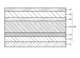
- FIG. 1 is a diagram schematically showing a configuration example of a photoelectric conversion element.
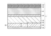
- FIG. 2 is a diagram schematically showing a configuration example of an image detection unit.
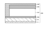
- FIG. 3 is a diagram schematically showing a configuration example of a fingerprint detection unit.
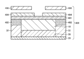
- FIG. 4 is a diagram schematically showing a configuration example of an image detection unit for an X-ray imaging apparatus.
- FIG. 5 is a diagram schematically showing a configuration example of a vein detection unit for the vein authentication device.
- FIG. 6 is a diagram schematically showing a configuration example of an image detection unit for an indirect TOF rangefinder.
- Non-fullerene compounds refer to compounds that are neither fullerenes nor fullerene derivatives.
- ⁇ -conjugated system means a system in which ⁇ electrons are delocalized to multiple bonds.
- polymer compound means a polymer having a molecular weight distribution and a polystyrene-equivalent number average molecular weight of 1 ⁇ 10 3 or more and 1 ⁇ 10 8 or less.
- structural units contained in the polymer compound are 100 mol % in total.
- a “structural unit” means a residue derived from a raw material compound (monomer) and present at least one in the compound and polymer compound of the present embodiment.
- a "hydrogen atom” may be a hydrogen atom or a deuterium atom.
- halogen atoms include fluorine atoms, chlorine atoms, bromine atoms, and iodine atoms.
- substituteduents include halogen atoms, alkyl groups, cycloalkyl groups, alkenyl groups, cycloalkenyl groups, alkynyl groups, cycloalkynyl groups, alkyloxy groups, cycloalkyloxy groups, alkylthio groups, cycloalkylthio groups, aryl groups, aryloxy groups, arylthio groups, monovalent heterocyclic groups, substituted amino groups, acyl groups, imine residues, amide groups, acid imide groups, substituted oxycarbonyl groups, cyano groups, alkylsulfonyl groups, and nitro groups mentioned.
- the number of carbon atoms usually does not include the number of carbon atoms of the substituent.
- the "alkyl group” may be linear, branched, or cyclic.
- the number of carbon atoms in the linear alkyl group is generally 1-50, preferably 1-30, more preferably 1-20, not including the number of carbon atoms in the substituents.
- the number of carbon atoms in the branched or cyclic alkyl group is usually 3 to 50, preferably 3 to 30, more preferably 4 to 20, not including the number of carbon atoms in substituents.
- alkyl groups include methyl, ethyl, n-propyl, isopropyl, n-butyl, isobutyl, tert-butyl, n-pentyl, isoamyl, 2-ethylbutyl, n- hexyl group, cyclohexyl group, n-heptyl group, cyclohexylmethyl group, cyclohexylethyl group, n-octyl group, 2-ethylhexyl group, 3-n-propylheptyl group, adamantyl group, n-decyl group, 3,7-dimethyl octyl group, 2-ethyloctyl group, 2-n-hexyl-decyl group, n-dodecyl group, tetradecyl group, hexadecyl group, octadecyl group and e
- the alkyl group may have a substituent.
- An alkyl group having a substituent is, for example, a group in which a hydrogen atom in the above-exemplified alkyl group is substituted with a substituent such as an alkyloxy group, an aryl group, or a fluorine atom.
- substituted alkyl examples include trifluoromethyl, pentafluoroethyl, perfluorobutyl, perfluorohexyl, perfluorooctyl, 3-phenylpropyl, and 3-(4-methylphenyl).
- propyl group 3-(3,5-dihexylphenyl)propyl group and 6-ethyloxyhexyl group.
- a “cycloalkyl group” may be a monocyclic group or a polycyclic group.
- a cycloalkyl group may have a substituent.
- the number of carbon atoms in the cycloalkyl group is usually 3-30, preferably 12-19, not including the number of carbon atoms in the substituents.
- cycloalkyl groups include unsubstituted alkyl groups such as cyclopentyl, cyclohexyl, cycloheptyl and adamantyl groups, and hydrogen atoms in these groups are alkyl groups, alkyloxy groups, aryl groups, fluorine Groups substituted with substituents such as atoms are included.
- cycloalkyl group having a substituent examples include a methylcyclohexyl group and an ethylcyclohexyl group.
- a "p-valent aromatic carbocyclic group" (p represents an integer of 1 or more) is a hydrogen atom directly bonded to a carbon atom constituting a ring from an optionally substituted aromatic hydrocarbon It means the remaining atomic groups excluding p atoms.
- the p-valent aromatic carbocyclic group may further have a substituent.
- the "aromatic carbocyclic ring” includes a structure in which two or more carbocyclic rings (aromatic rings) are crossed by a group (substituent) containing a hetero atom, for example.
- Aryl group is a monovalent aromatic carbocyclic group, which is an optionally substituted aromatic hydrocarbon remaining after removing one hydrogen atom directly bonded to a carbon atom constituting the ring means the atomic group of
- the aryl group may have a substituent.
- aryl groups include phenyl, 1-naphthyl, 2-naphthyl, 1-anthracenyl, 2-anthracenyl, 9-anthracenyl, 1-pyrenyl, 2-pyrenyl, and 4-pyrenyl groups.
- 2-fluorenyl group, 3-fluorenyl group, 4-fluorenyl group, 2-phenylphenyl group, 3-phenylphenyl group, 4-phenylphenyl group, and hydrogen atoms in these groups are alkyl groups, alkyloxy groups , an aryl group, and a group substituted with a substituent such as a fluorine atom.
- Alkyloxy group may be linear, branched, or cyclic.
- the number of carbon atoms in the straight-chain alkyloxy group is generally 1-40, preferably 1-10, not including the number of carbon atoms in the substituents.
- the number of carbon atoms in the branched or cyclic alkyloxy group is usually 3-40, preferably 4-10, not including the number of carbon atoms in the substituents.
- the alkyloxy group may have a substituent.
- alkyloxy groups include methoxy, ethoxy, n-propyloxy, isopropyloxy, n-butyloxy, isobutyloxy, tert-butyloxy, n-pentyloxy and n-hexyloxy groups.
- the cycloalkyl group possessed by the "cycloalkyloxy group” may be a monocyclic group or a polycyclic group.
- a cycloalkyloxy group may have a substituent.
- the number of carbon atoms in the cycloalkyloxy group is usually 3-30, preferably 12-19, not including the number of carbon atoms in the substituent.
- cycloalkyloxy groups include unsubstituted cycloalkyloxy groups such as cyclopentyloxy, cyclohexyloxy, and cycloheptyloxy groups, and hydrogen atoms in these groups substituted with fluorine atoms or alkyl groups. and the groups described above.
- the number of carbon atoms in the "aryloxy group” is usually 6 to 60, preferably 6 to 48, not including the number of carbon atoms in the substituents.
- the aryloxy group may have a substituent.
- Specific examples of the aryloxy group include a phenoxy group, a 1-naphthyloxy group, a 2-naphthyloxy group, a 1-anthracenyloxy group, a 9-anthracenyloxy group, a 1-pyrenyloxy group, and these groups.
- a group in which a hydrogen atom in is substituted with a substituent such as an alkyl group, an alkyloxy group, or a fluorine atom.
- Alkylthio group may be linear, branched, or cyclic.
- the number of carbon atoms in the straight-chain alkylthio group is generally 1-40, preferably 1-10, not including the number of carbon atoms in the substituents.
- the number of carbon atoms in the branched or cyclic alkylthio group is usually 3-40, preferably 4-10, not including the number of carbon atoms in the substituents.
- the alkylthio group may have a substituent.
- alkylthio groups include methylthio, ethylthio, propylthio, isopropylthio, butylthio, isobutylthio, tert-butylthio, pentylthio, hexylthio, cyclohexylthio, heptylthio, octylthio, 2 -ethylhexylthio, nonylthio, decylthio, 3,7-dimethyloctylthio, laurylthio, and trifluoromethylthio groups.
- the cycloalkyl group possessed by the "cycloalkylthio group” may be a monocyclic group or a polycyclic group.
- a cycloalkylthio group may have a substituent.
- the number of carbon atoms in the cycloalkylthio group is usually 3-30, preferably 12-19, not including the number of carbon atoms in the substituent.
- a cyclohexylthio group is mentioned as an example of the cycloalkylthio group which may have a substituent.
- the number of carbon atoms in the "arylthio group” is usually 6-60, preferably 6-48, not including the number of carbon atoms in the substituent.
- the arylthio group may have a substituent.
- the arylthio group include a phenylthio group and a C1-C12 alkyloxyphenylthio group (C1-C12 indicates that the number of carbon atoms in the group immediately following it is 1-12. The same applies below. .), C1-C12 alkylphenylthio groups, 1-naphthylthio groups, 2-naphthylthio groups, and pentafluorophenylthio groups.
- p-valent heterocyclic group means p hydrogen atoms among the hydrogen atoms directly bonded to the carbon atoms or heteroatoms constituting the ring from the optionally substituted heterocyclic compound means the rest of the atomic groups excluding
- the p-valent heterocyclic group may further have a substituent.
- the number of carbon atoms in the p-valent heterocyclic group is usually 2 to 30, preferably 2 to 6, not including the number of carbon atoms in the substituents.
- heterocyclic compound may have include halogen atoms, alkyl groups, aryl groups, alkyloxy groups, aryloxy groups, alkylthio groups, arylthio groups, monovalent heterocyclic groups, substituted amino groups, acyl groups, imine residues, amide groups, acid imide groups, substituted oxycarbonyl groups, alkenyl groups, alkynyl groups, cyano groups, and nitro groups.
- the p-valent heterocyclic group includes a "p-valent aromatic heterocyclic group".
- p-valent aromatic heterocyclic group from an optionally substituted aromatic heterocyclic compound, out of the hydrogen atoms directly bonded to the carbon atoms or heteroatoms constituting the ring p means the remaining atomic groups excluding the hydrogen atoms of The p-valent aromatic heterocyclic group may further have a substituent.
- Aromatic heterocyclic compounds include not only compounds in which the heterocycle itself exhibits aromaticity, but also compounds in which an aromatic ring is fused to a heterocycle, even if the heterocycle itself does not exhibit aromaticity. be.
- aromatic heterocyclic compounds specific examples of compounds in which the heterocycle itself exhibits aromaticity include oxadiazole, thiadiazole, thiazole, oxazole, thiophene, pyrrole, phosphole, furan, pyridine, pyrazine, pyrimidine, and triazine. , pyridazine, quinoline, isoquinoline, carbazole, and dibenzophosphole.
- aromatic heterocyclic compounds specific examples of compounds in which the aromatic heterocyclic ring itself does not show aromaticity and the aromatic ring is fused to the heterocyclic ring include phenoxazine, phenothiazine, dibenzoborol, dibenzo Siloles, and benzopyrans.
- the number of carbon atoms in the monovalent heterocyclic group is usually 2-60, preferably 4-20, not including the number of carbon atoms in the substituent.
- the monovalent heterocyclic group may have a substituent, and specific examples of the monovalent heterocyclic group include thienyl, pyrrolyl, furyl, pyridyl, piperidyl, quinolyl, isoquinolyl group, pyrimidinyl group, triazinyl group, and groups in which hydrogen atoms in these groups are substituted with alkyl groups, alkyloxy groups, and the like.
- Substituted amino group means an amino group having a substituent.
- substituents possessed by the amino group include alkyl groups, aryl groups, and monovalent heterocyclic groups, with alkyl groups, aryl groups, and monovalent heterocyclic groups being preferred.
- the substituted amino group usually has 2 to 30 carbon atoms.
- substituted amino groups include dialkylamino groups such as dimethylamino group and diethylamino group; diphenylamino group, bis(4-methylphenyl)amino group, bis(4-tert-butylphenyl)amino group, bis(3, and diarylamino groups such as 5-di-tert-butylphenyl)amino group.
- the "acyl group” may have a substituent.
- the number of carbon atoms in the acyl group is usually 2-20, preferably 2-18, not including the number of carbon atoms in the substituents.
- Specific examples of acyl groups include acetyl, propionyl, butyryl, isobutyryl, pivaloyl, benzoyl, trifluoroacetyl, and pentafluorobenzoyl groups.
- Imine residue means an atomic group remaining after removing one hydrogen atom directly bonded to a carbon atom or a nitrogen atom that constitutes a carbon atom-nitrogen atom double bond from an imine compound.
- An "imine compound” means an organic compound having a carbon atom-nitrogen atom double bond in the molecule.
- imine compounds include aldimines, ketimines, and compounds in which a hydrogen atom bonded to a nitrogen atom constituting a carbon atom-nitrogen double bond in aldimines is substituted with an alkyl group or the like.
- the imine residue usually has 2 to 20 carbon atoms, preferably 2 to 18 carbon atoms.
- Examples of imine residues include groups represented by the following structural formulas.
- Amido group means an atomic group remaining after removing one hydrogen atom bonded to a nitrogen atom from amide.
- the amide group usually has 1 to 20 carbon atoms, preferably 1 to 18 carbon atoms.
- Specific examples of the amide group include a formamide group, an acetamide group, a propioamide group, a butyroamide group, a benzamide group, a trifluoroacetamide group, a pentafluorobenzamide group, a diformamide group, a diacetamide group, a dipropioamide group, a dibutyroamide group, and a dibenzamide group. , a ditrifluoroacetamide group, and a dipentafluorobenzamide group.
- Acid imide group means an atomic group remaining after removing one hydrogen atom bonded to a nitrogen atom from an acid imide.
- the number of carbon atoms in the acid imide group is generally 4-20.
- Specific examples of acid imide groups include groups represented by the following structural formulas.
- R' represents an alkyl group, an aryl group, an arylalkyl group, or a monovalent heterocyclic group.
- the number of carbon atoms in the substituted oxycarbonyl group is usually 2 to 60, preferably 2 to 48, not including the number of carbon atoms in the substituent.
- substituted oxycarbonyl groups include methoxycarbonyl, ethoxycarbonyl, propoxycarbonyl, isopropoxycarbonyl, butoxycarbonyl, isobutoxycarbonyl, tert-butoxycarbonyl, pentyloxycarbonyl and hexyloxycarbonyl groups.
- Alkenyl group may be linear, branched, or cyclic.
- the number of carbon atoms in the straight-chain alkenyl group is usually 2-30, preferably 3-20, not including the number of carbon atoms in the substituents.
- the number of carbon atoms in the branched or cyclic alkenyl group is usually 3 to 30, preferably 4 to 20, not including the number of carbon atoms in substituents.
- the alkenyl group may have a substituent.
- alkenyl groups include vinyl, 1-propenyl, 2-propenyl, 2-butenyl, 3-butenyl, 3-pentenyl, 4-pentenyl, 1-hexenyl and 5-hexenyl groups. , 7-octenyl groups, and groups in which hydrogen atoms in these groups are substituted with alkyl groups, alkyloxy groups, aryl groups, and fluorine atoms.
- a "cycloalkenyl group” may be a monocyclic group or a polycyclic group.
- a cycloalkenyl group may have a substituent.
- the number of carbon atoms in the cycloalkenyl group is usually 3-30, preferably 12-19, not including the number of carbon atoms in the substituents.
- cycloalkenyl groups include unsubstituted cycloalkenyl groups such as cyclohexenyl, and groups in which hydrogen atoms in these groups are substituted with alkyl groups, alkyloxy groups, aryl groups, and fluorine atoms. mentioned.
- substituted cycloalkenyl groups include a methylcyclohexenyl group and an ethylcyclohexenyl group.
- Alkynyl group may be linear, branched, or cyclic.
- the number of carbon atoms in the linear alkenyl group is usually 2 to 20, preferably 3 to 20, not including the number of carbon atoms in the substituents.
- the number of carbon atoms in the branched or cyclic alkenyl group is usually 4 to 30, preferably 4 to 20, not including the number of carbon atoms in the substituents.
- the alkynyl group may have a substituent.
- alkynyl groups include ethynyl, 1-propynyl, 2-propynyl, 2-butynyl, 3-butynyl, 3-pentynyl, 4-pentynyl, 1-hexynyl and 5-hexynyl groups. , and groups in which hydrogen atoms in these groups are substituted with alkyloxy groups, aryl groups, and fluorine atoms.
- a “cycloalkynyl group” may be a monocyclic group or a polycyclic group.
- a cycloalkynyl group may have a substituent.
- the number of carbon atoms in the cycloalkynyl group is generally 4-30, preferably 12-19, not including the number of carbon atoms in the substituents.
- cycloalkynyl groups include unsubstituted cycloalkynyl groups such as cyclohexynyl groups, and groups in which hydrogen atoms in these groups are substituted with alkyl groups, alkyloxy groups, aryl groups, and fluorine atoms. be done.
- substituted cycloalkynyl groups include a methylcyclohexynyl group and an ethylcyclohexynyl group.
- alkylsulfonyl group may be linear or branched.
- the alkylsulfonyl group may have a substituent.
- the number of carbon atoms in the alkylsulfonyl group is usually 1-30, not including the number of carbon atoms in the substituents.
- Specific examples of alkylsulfonyl groups include methylsulfonyl, ethylsulfonyl, and dodecylsulfonyl groups.
- “Ink” means a liquid used in the coating method, and is not limited to colored liquids.
- coating method includes a method of forming a film (layer) using a liquid substance, for example, slot die coating method, slit coating method, knife coating method, spin coating method, casting method, micro gravure coating method. , gravure coating method, bar coating method, roll coating method, wire bar coating method, dip coating method, spray coating method, screen printing method, gravure printing method, flexographic printing method, offset printing method, inkjet coating method, dispenser printing method, A nozzle coating method and a capillary coating method can be mentioned.
- the ink may be a solution, or may be a dispersion liquid such as a dispersion liquid, an emulsion (emulsion), or a suspension (suspension).
- a dispersion liquid such as a dispersion liquid, an emulsion (emulsion), or a suspension (suspension).
- Absorption peak wavelength is a parameter specified based on the absorption peak of the absorption spectrum measured in a predetermined wavelength range, and refers to the wavelength of the absorption peak with the highest absorbance among the absorption peaks of the absorption spectrum.
- External Quantum Efficiency is also called EQE (External Quantum Efficiency), and the number of electrons that can be taken out of the photoelectric conversion element among the generated electrons with respect to the number of photons irradiated to the photoelectric conversion element. is expressed as a ratio (%).
- the compound of the present embodiment can be suitably used as a semiconductor material, particularly for the active layer of a photoelectric conversion device. Note that whether the compound of the present embodiment functions as a p-type semiconductor material or an n-type semiconductor material in the active layer depends on the HOMO energy level value or the LUMO energy level value of the selected compound. can be determined relatively from The compound of the present embodiment can be suitably used, particularly as an n-type semiconductor material, in the active layer of a photoelectric conversion device.
- the relationship between the HOMO and LUMO energy level values of the p-type semiconductor material contained in the active layer and the HOMO and LUMO energy level values of the n-type semiconductor material is used to function the photoelectric conversion element (light detection element). can be appropriately set within a range where
- the compound of this embodiment is a compound represented by the following formula (I).
- a 1 and A 2 are each independently an electron-withdrawing monovalent group; P is a divalent group represented by the following formula (1).
- X represents a group represented by -S-, a group represented by -O-, a group represented by -Se-, or a group represented by -N(R)-
- Ar 1 and Ar 2 each independently have an optionally substituted aromatic carbocyclic ring in which a plurality of ring structures may be conden
- the compound of the present embodiment is a non-fullerene compound represented by the above formula (I), wherein the electron-withdrawing monovalent groups A 1 and A 2 are represented by the formula (1) 2 It is a compound bound to both ends of P, which is a valence group.
- a 1 and A 2 are electron-withdrawing monovalent groups.
- a 1 and A 2 may be the same group, and from the viewpoint of facilitating synthesis of the compound, A 1 and A 2 are preferably the same group.
- Examples of A 1 and A 2 include groups represented by —CH ⁇ C(—CN) 2 and groups represented by the following formulas (a-1) to (a-9).
- T represents an optionally substituted carbocyclic ring or an optionally substituted heterocyclic ring.
- Carbocyclic and heterocyclic rings may be monocyclic or condensed. When these rings have multiple substituents, the multiple substituents may be the same or different.
- Examples of the optionally substituted carbocyclic ring represented by T include aromatic carbocyclic rings, preferably aromatic carbocyclic rings.
- Specific examples of optionally substituted carbocyclic rings represented by T include benzene ring, naphthalene ring, anthracene ring, tetracene ring, pentacene ring, pyrene ring and phenanthrene ring, preferably benzene They are a ring, a naphthalene ring and a phenanthrene ring, more preferably a benzene ring and a naphthalene ring, still more preferably a benzene ring. These rings may have a substituent.
- Examples of the optionally substituted heterocyclic ring represented by T include aromatic heterocyclic rings, preferably aromatic carbocyclic rings.
- Specific examples of the optionally substituted heterocyclic ring represented by T include pyridine ring, pyridazine ring, pyrimidine ring, pyrazine ring, pyrrole ring, furan ring, thiophene ring, imidazole ring, oxazole ring, thiazole and a thienothiophene ring, preferably a thiophene ring, a pyridine ring, a pyrazine ring, a thiazole ring, and a thienothiophene ring, more preferably a thiophene ring. These rings may have a substituent.
- substituents that the carbocyclic or heterocyclic ring represented by T may have include halogen atoms, alkyl groups, alkyloxy groups, aryl groups, cyano groups and monovalent heterocyclic groups, preferably fluorine atom, chlorine atom, alkyloxy group having 1 to 6 carbon atoms and/or alkyl group having 1 to 6 carbon atoms.
- X 7 is a hydrogen atom or a halogen atom, a cyano group, an optionally substituted alkyl group, an optionally substituted alkyloxy group, an optionally substituted aryl group, or represents a monovalent heterocyclic group.
- X7 is preferably a cyano group.
- R a1 , R a2 , R a3 , R a4 , and R a5 each independently represent a hydrogen atom, an optionally substituted alkyl group, a halogen atom, an optionally substituted alkyl represents an oxy group, an optionally substituted aryl group or a monovalent heterocyclic group, preferably an optionally substituted alkyl group or an optionally substituted aryl group is.
- R a6 and R a7 each independently represent a hydrogen atom, a halogen atom, an optionally substituted alkyl group, an optionally substituted cycloalkyl group, or a substituted an alkyloxy group that may have a substituent, a cycloalkyloxy group that may have a substituent, a monovalent aromatic carbocyclic group that may have a substituent, or a monovalent that may have a substituent and a plurality of R a6 and R a7 may be the same or different.
- electron-withdrawing monovalent groups represented by A 1 and A 2 include the following formulas (a-1-1) to (a-1-4), and formula (a-5- 1), groups represented by formula (a-6-1), formula (a-6-2) and formula (a-7-1).
- Formula (a-1-1) to formula (a-1-4), and formula (a-5-1), formula (a-6-1), formula (a-6-2) and formula (a- 7-1) Medium, multiple R a10 each independently represent a hydrogen atom or a substituent, R a1 , R a2 , R a3 , R a4 and R a5 are each independently as defined above.
- R a10 is preferably a hydrogen atom, a halogen atom, an alkyloxy group, a cyano group or an alkyl group.
- R a1 , R a2 , R a3 , R a4 and R a5 are preferably an optionally substituted alkyl group or an optionally substituted aryl group.
- a 1 and A 2 are each independently preferably an electron-withdrawing group containing one or more selected from the group consisting of a cyano group, a carbonyl group and a thiocarbonyl group.
- Preferred examples of the electron-withdrawing monovalent groups represented by A 1 and A 2 include groups represented by the following formulae.
- P P in the compound represented by the formula (I) is a divalent group represented by the following formula (1).
- P is a divalent radical containing one or more pairs of atoms that are ⁇ -bonded to each other, with a ⁇ -electron cloud extending throughout P.
- the compound represented by the formula (I) is preferably a compound in which the ⁇ -electron cloud extends over all of A 1 , A 2 and P.
- X represents a group represented by -S-, a group represented by -O-, a group represented by -Se-, or a group represented by -NR-.
- X is preferably a group represented by -S- or a group represented by -O- from the viewpoint of more effectively reducing dark current in a photoelectric conversion element (photodetector), and -S A group represented by - is more preferable.
- R is a hydrogen atom, a halogen atom, an optionally substituted alkyl group, an optionally substituted cycloalkyl group, an optionally substituted aryl group, a substituted optionally substituted alkyloxy group, optionally substituted cycloalkyloxy group, optionally substituted aryloxy group, optionally substituted alkylthio group , optionally substituted cycloalkylthio group, optionally substituted arylthio group, optionally substituted monovalent heterocyclic group, optionally substituted optionally substituted amino group, optionally substituted acyl group, optionally substituted imine residue, optionally substituted amide group, optionally substituted acid imide group, optionally substituted oxycarbonyl group, optionally substituted alkenyl group, optionally substituted cycloalkenyl group, substituted optionally substituted alkynyl group, optionally substituted cycloalkynyl group, cyano group, nitro group, group represented by a
- R 1 and R 2 each independently have the same meaning as R already explained, and the preferred examples are also the same as R, so detailed explanation thereof will be omitted.
- Ar 1 and Ar 2 each independently have an optionally substituted aromatic carbocyclic ring in which a plurality of ring structures may be condensed or may optionally have a substituent or a plurality of It is an aromatic heterocyclic ring in which the ring structure may be further condensed.
- Ar 1 and Ar 2 each independently preferably have a ring structure containing an optionally substituted thiophene ring, and are composed only of an optionally substituted thiophene ring. good too.
- the number of carbon atoms in the aromatic carbocyclic rings represented by Ar 1 and Ar 2 is usually 6-60, preferably 6-20, not including the number of carbon atoms in the substituents.
- the number of carbon atoms in the aromatic carbocyclic ring including substituents is usually 6-100.
- aromatic carbocyclic rings represented by Ar 1 and Ar 2 include aromatic carbocyclic rings represented by the following formulas (001) to (010). These aromatic carbocyclic rings may further have substituents.
- aromatic carbocyclic rings represented by Ar 1 and Ar 2 represented by the above formulas (001) to (010) include aromatic carbocyclic rings represented by the following formulae.
- the number of carbon atoms in the aromatic heterocycle represented by Ar 1 and Ar 2 is generally 2-60, preferably 4-60, more preferably 4-20.
- substituents which the aromatic heterocycles represented by Ar 1 and Ar 2 may have include halogen atoms, optionally substituted alkyl groups, aryl group, optionally substituted alkyloxy group, optionally substituted aryloxy group, optionally substituted alkylthio group, optionally substituted arylthio group, optionally substituted monovalent heterocyclic group, optionally substituted amino group, optionally substituted acyl group, substituted optionally substituted imine residue, optionally substituted amide group, optionally substituted acid imide group, optionally substituted oxycarbonyl group, substituent An alkenyl group which may have one, an alkynyl group which may have one or more substituents, a cyano group and a nitro group may be mentioned.
- aromatic heterocycles represented by Ar 1 and Ar 2 include groups represented by the following formulas (101) to (125). These aromatic heterocycles may further have a substituent.
- Ar 1 and Ar 2 are preferably a thiophene ring optionally having a substituent or a ring structure represented by the following formula.
- R, R1 and R2 are as defined above.
- Ar 1 and Ar 2 include ring structures represented by the following formulae.
- Y 1 and Y 2 are a group represented by -NR-, a group represented by -S-, or a group represented by -O-CR 1 R 2 - is preferably a group represented by -NR- or a group represented by -S- is more preferable.
- Y 1 and Y 2 are groups represented by -NR-, or P is a divalent group represented by the following formula (2). Preferably.
- Preferred examples of X, R, R 1 and R 2 are as already described in formula (1) above.
- Preferred examples of the divalent group represented by formula (1) in which Y 1 and Y 2 are groups represented by —NR— include groups represented by the following formula (1-1).
- X, R, Ar3 , Ar4 , m and n are as defined above.
- divalent group represented by formula (1-1) More specific and preferred examples of the divalent group represented by formula (1-1) above include a divalent group represented by the following formula.
- Preferred examples of the divalent group represented by formula (1) include groups represented by the following formula (1-2).
- Preferred examples of the divalent group represented by the formula (1-2) include groups having structures represented by the following formulas (1-2a), (1-2b) and (1-2c) is mentioned.
- R is as defined above.
- divalent group having a structure represented by formula (1-2a), formula (1-2b) and formula (1-2c) include a divalent group represented by the following formula: mentioned.
- divalent group represented by formula (1) include groups represented by the following formula (1-3).
- Preferred examples of the divalent group represented by the formula (1-3) include groups represented by the following formula.
- Ar 3 and Ar 4 are respectively plural, the plural Ar 3 and the plural Ar 4 may be the same or different.
- Ar 3 and Ar 4 are preferably divalent aromatic heterocyclic groups containing a thiophene ring, optionally having a substituent, and optionally having a plurality of condensed ring structures.
- the divalent aromatic carbocyclic group (arylene group) represented by Ar 3 and Ar 4 is specifically an aromatic hydrocarbon optionally having a substituent, a hydrogen atom means the remaining atomic groups excluding two of
- aromatic hydrocarbons also include compounds having a condensed ring in which a plurality of ring structures are condensed.
- the number of carbon atoms in the divalent aromatic carbocyclic group represented by Ar 3 and Ar 4 is usually 6-60, preferably 6-20, not including the number of carbon atoms in the substituents.
- the number of carbon atoms in the aromatic carbocyclic group including substituents is usually 6-100.
- Examples of the divalent aromatic carbocyclic groups represented by Ar 3 and Ar 4 include divalent aromatic carbocyclic groups represented by the following formulas (201) to (210). These groups may further have a substituent.
- the divalent aromatic hydrocarbon groups represented by Ar 3 and Ar 4 are preferably divalent aromatic carbocyclic groups represented by the following formulae.
- the number of carbon atoms in the divalent aromatic heterocyclic group represented by Ar 3 and Ar 4 is generally 2-60, preferably 4-60, more preferably 4-20.
- Examples of the substituent that the divalent aromatic heterocyclic group represented by Ar 3 and Ar 4 may have include a halogen atom, an optionally substituted alkyl group, and a optionally substituted aryl group, optionally substituted alkyloxy group, optionally substituted aryloxy group, optionally substituted alkylthio group, optionally substituted optionally substituted arylthio group, optionally substituted monovalent heterocyclic group, optionally substituted amino group, optionally substituted acyl group, substituted imine residue optionally having a group, an amide group optionally having a substituent, an acid imide group optionally having a substituent, a substituted oxycarbonyl group optionally having a substituent , an optionally substituted alkenyl group, an optionally substituted alkynyl group, a cyano group, and a nitro group.
- divalent aromatic heterocyclic groups represented by Ar 3 and Ar 4 include divalent aromatic heterocyclic groups represented by the following formulas (301) to (343). These groups may further have a substituent.
- divalent aromatic heterocyclic group represented by Ar 3 and Ar 4 a divalent aromatic heterocyclic group represented by the following formula is preferable. These groups may further have a substituent.
- divalent aromatic heterocyclic groups represented by Ar 3 and Ar 4 represented by the above formulas include divalent groups represented by the following formulas.
- n and m are each independently 0, 1, 2 or 3, and from the viewpoint of facilitating synthesis, n and m are each independently 0 or 1 is preferred. Therefore, the compound of this embodiment may not contain either one or both of Ar 3 and Ar 4 .
- Preferred specific examples of the compound represented by formula (I) of the present embodiment include compounds represented by the following formula.
- the compound of the present embodiment can be suitably used as a material for the active layer of a photoelectric conversion device (details will be described later), particularly as a non-fullerene compound that is an n-type semiconductor material.
- the dark current in the photoelectric conversion device can be more effectively reduced.
- Two or more of the compounds of this embodiment used as the n-type semiconductor material may be included as materials for the active layer.
- the compound of the present embodiment can be obtained by any suitable conventionally known method or It can be produced (synthesized) by the method shown in the examples described later.
- the present invention also relates to compounds represented by the following formula (3). That is, the present invention also relates to starting compounds that are suitable for the production of the compounds of formula (I) already explained.
- X represents a group represented by -S-, a group represented by -O-, a group represented by -Se-, or a group represented by -N(R)-
- Ar 1 and Ar 2 each independently have an optionally substituted aromatic carbocyclic ring in which a plurality of ring structures may be condensed or may optionally have a substituent or
- X, Y 1 , Y 2 , Ar 1 , Ar 2 , R, R 1 and R 2 in formula (3) are as already described in formula (1).
- Y 1 and Y 2 are preferably groups represented by -NR-.
- the compound represented by the formula (3) is preferably a compound represented by the following formula (4).
- W represents a hydrogen atom, a halogen atom, a borate residue, a dihydroxyboryl group, a formyl group, a vinyl group or a substituted stannyl group. Two W may be the same or different.
- Substituted stannyl groups include groups represented by -SnR 100 3 and the like.
- R 100 represents a monovalent organic group.
- Monovalent organic groups include, for example, alkyl groups and aryl groups.
- the alkyl group represented by R 100 includes methyl, ethyl, propyl, isopropyl, butyl, isobutyl, sec-butyl, tert-butyl, pentyl, isopentyl, 2-methylbutyl and 1-methylbutyl.
- hexyl group isohexyl group, 3-methylpentyl group, 2-methylpentyl group, 1-methylpentyl group, heptyl group, octyl group, isooctyl group, 2-ethylhexyl group, nonyl group, decyl group, undecyl group, dodecyl chain alkyl groups such as tetradecyl group, hexadecyl group, octadecyl group and eicosyl group; and cycloalkyl groups such as cyclopentyl group, cyclohexyl group and adamantyl group.
- the aryl group includes a phenyl group and a naphthyl group.
- Preferred substituted stannyl groups are -SnMe 3 , -SnEt 3 , -SnBu 3 and -SnPh 3 , and more preferred are -SnMe 3 , -SnEt 3 and -SnBu 3 .
- Me represents a methyl group
- Et represents an ethyl group
- Bu represents a butyl group
- Ph represents a phenyl group.
- a boric acid ester residue represents a group obtained by removing a hydroxyl group from a boric acid diester.
- Specific examples of the boric acid ester residue include groups represented by the following formulae.
- Me represents a methyl group and Et represents an ethyl group.
- Suitable specific examples of the compounds represented by the formulas (3) and (4) include compounds represented by the following formulas.
- the active layer of the photoelectric conversion element may contain only the compound of this embodiment as an n-type semiconductor material, or may contain a compound other than the compound of this embodiment as an additional n-type semiconductor material. good too.
- Compounds other than the compounds of the present embodiment that can be included as additional n-type semiconductor materials may be low-molecular-weight compounds or high-molecular-weight compounds.
- n-type semiconductor materials (electron-accepting compounds) other than the low-molecular compound "compound of the present embodiment” examples include oxadiazole derivatives, anthraquinodimethane and its derivatives, benzoquinone and its derivatives, naphthoquinone and its derivatives. derivatives, anthraquinone and its derivatives, tetracyanoanthraquinodimethane and its derivatives, fluorenone derivatives, diphenyldicyanoethylene and its derivatives, diphenoquinone derivatives, metal complexes of 8-hydroxyquinoline and its derivatives, and phenanthrene derivatives such as bathocuproine. be done.
- n-type semiconductor materials other than the "compound of the present embodiment" which is a polymer compound include polyvinylcarbazole and its derivatives, polysilane and its derivatives, polysiloxane derivatives having an aromatic amine structure in the side chain or main chain, polyaniline and its derivatives, polythiophene and its derivatives, polypyrrole and its derivatives, polyphenylene vinylene and its derivatives, polythienylene vinylene and its derivatives, polyquinoline and its derivatives, polyquinoxaline and its derivatives, and polyfluorene and its derivatives .
- Compounds other than “compounds of the present embodiment” may include fullerene derivatives.
- the fullerene derivative refers to a compound in which at least a portion of fullerene ( C60 fullerene, C70 fullerene, C76 fullerene, C78 fullerene, and C84 fullerene) is modified. In other words, it refers to a compound having one or more groups attached to the fullerene skeleton.
- the fullerene derivative of C60 fullerene may be particularly referred to as " C60 fullerene derivative”
- the fullerene derivative of C70 fullerene may be referred to as " C70 fullerene derivative”.
- the fullerene derivative that can be used as an n-type semiconductor material other than the "compound of the present embodiment” is not particularly limited as long as it does not impair the purpose of the present invention.
- C60 fullerene derivative that can be used as the n-type semiconductor material other than the "compound of the present embodiment” include the following compounds.
- R is as defined above.
- the multiple R's may be the same or different.
- C70 fullerene derivatives include the following compounds.
- Photoelectric conversion element The photoelectric conversion element according to the present embodiment includes an anode, a cathode, and an active layer provided between the anode and the cathode and containing a p-type semiconductor material and an n-type semiconductor material, A photoelectric conversion device containing the compound of the present embodiment described above as the n-type semiconductor material.
- the photoelectric conversion element of the present embodiment by having the above configuration, a decrease in external quantum efficiency due to heat treatment in the manufacturing process of the photoelectric conversion element or the process of incorporating the photoelectric conversion element into a device to which the photoelectric conversion element is applied is suppressed. and can effectively improve the heat resistance.
- FIG. 1 is a diagram schematically showing the configuration of the photoelectric conversion element of this embodiment.
- the photoelectric conversion element 10 is provided on a support substrate 11.
- the photoelectric conversion element 10 includes an anode 12 provided in contact with a support substrate 11, a hole transport layer 13 provided in contact with the anode 12, and a hole transport layer 13 provided in contact with the hole transport layer 13. an active layer 14 , an electron transport layer 15 provided in contact with the active layer 14 , and a cathode 16 provided in contact with the electron transport layer 15 .
- a sealing member 17 is further provided so as to be in contact with the cathode 16 .
- a photoelectric conversion element is usually formed on a substrate (support substrate). Further, it may be further sealed with a substrate (sealing substrate).
- a substrate substrate (sealing substrate).
- the material of the substrate is not particularly limited as long as it is a material that does not chemically change when the layer containing an organic compound is formed.
- the electrode on the opposite side of the electrode provided on the opaque substrate is preferably a transparent or translucent electrode.
- a photoelectric conversion element includes a pair of electrodes, an anode and a cathode. At least one of the anode and the cathode is preferably a transparent or translucent electrode in order to allow light to enter.
- Examples of materials for transparent or semi-transparent electrodes include conductive metal oxide films and semi-transparent metal thin films. Specifically, indium oxide, zinc oxide, tin oxide, and their composites indium tin oxide (ITO), indium zinc oxide (IZO), conductive materials such as NESA, gold, platinum, silver, copper. ITO, IZO, and tin oxide are preferable as materials for transparent or translucent electrodes. Moreover, as the electrode, a transparent conductive film using an organic compound such as polyaniline and its derivatives, polythiophene and its derivatives as a material may be used. The transparent or translucent electrode can be either the anode or the cathode.
- the other electrode may be an electrode with low light transmittance.
- materials for electrodes with low light transmittance include metals and conductive polymers.
- Specific examples of low light transmissive electrode materials include lithium, sodium, potassium, rubidium, cesium, magnesium, calcium, strontium, barium, aluminum, scandium, vanadium, zinc, yttrium, indium, cerium, samarium, europium, Metals such as terbium, ytterbium, and alloys of two or more thereof, or one or more of these metals together with gold, silver, platinum, copper, manganese, titanium, cobalt, nickel, tungsten and tin alloys with one or more metals selected from the group consisting of graphite, graphite intercalation compounds, polyaniline and its derivatives, polythiophene and its derivatives.
- Alloys include magnesium-silver alloys, magnesium-indium alloys, magnesium-aluminum alloys, indium-silver alloys, lithium-aluminum alloys, lithium-magnesium alloys, lithium-indium alloys, and calcium-aluminum alloys.
- the active layer included in the photoelectric conversion element of the present embodiment is assumed to have a bulk heterojunction structure and includes a p-type semiconductor material and an n-type semiconductor material, and the active layer is an n-type semiconductor material. includes the compound of the present embodiment (details will be described later).
- the thickness of the active layer is not particularly limited.
- the thickness of the active layer can be any suitable thickness considering the balance between suppression of dark current and extraction of the generated photocurrent.
- the thickness of the active layer is preferably 100 nm or more, more preferably 150 nm or more, and even more preferably 200 nm or more, particularly from the viewpoint of further reducing dark current.
- the thickness of the active layer is preferably 10 ⁇ m or less, more preferably 5 ⁇ m or less, and even more preferably 1 ⁇ m or less.
- the active layer is formed by a process that includes heating at a heating temperature of 200°C or higher (details will be described later).
- a p-type semiconductor material that can be suitably used as a material for the active layer according to this embodiment in combination with the n-type semiconductor material, which is the compound of this embodiment already described, will be described.
- the p-type semiconductor material is preferably a polymer compound having a predetermined polystyrene-equivalent weight-average molecular weight.
- the weight average molecular weight in terms of polystyrene means the weight average molecular weight calculated using a standard sample of polystyrene using gel permeation chromatography (GPC).
- the polystyrene-equivalent weight average molecular weight of the p-type semiconductor material is preferably 3,000 or more and 500,000 or less, particularly from the viewpoint of improving solubility in solvents.
- the p-type semiconductor material is a ⁇ -conjugated polymer compound (DA-type conjugated polymer It is also referred to as a compound.). It should be noted that which is the donor structural unit or which is the acceptor structural unit can be relatively determined from the energy level of the HOMO or LUMO.
- the donor structural unit is a structural unit with an excess of ⁇ electrons
- the acceptor structural unit is a structural unit with a ⁇ electron deficiency.
- the structural unit that can constitute the p-type semiconductor material may be a structural unit in which a donor structural unit and an acceptor structural unit are directly bonded, or a donor structural unit and an acceptor structural unit.
- Structural units linked via spacers are also included.
- Examples of p-type semiconductor materials that are polymer compounds include polyvinylcarbazole and its derivatives, polysilane and its derivatives, polysiloxane derivatives containing an aromatic amine structure in the side chain or main chain, polyaniline and its derivatives, polythiophene and its derivatives. , polypyrrole and its derivatives, polyphenylene vinylene and its derivatives, polythienylene vinylene and its derivatives, polyfluorene and its derivatives.
- the p-type semiconductor material of this embodiment is preferably a polymer compound containing a structural unit represented by the following formula (II).
- a structural unit represented by the following formula (II) is usually a donor structural unit in the present embodiment.
- Ar 5 and Ar 6 represent an optionally substituted trivalent aromatic heterocyclic group, and Z is represented by the following formulas (Z-1) to (Z-7). represents the group represented.
- R is as defined above. In each of formulas (Z-1) to (Z-7), when there are two R's, the two R's may be the same or different.
- the aromatic heterocycles that can constitute Ar 5 and Ar 6 include, in addition to monocyclic rings and condensed rings in which the heterocycle itself exhibits aromaticity, even if the heterocycle itself does not exhibit aromaticity.
- a ring in which an aromatic ring is condensed to a heterocyclic ring is included.
- Each of the aromatic heterocycles that can constitute Ar 5 and Ar 6 may be a monocyclic ring or a condensed ring.
- the aromatic heterocycle is a condensed ring, all of the rings constituting the condensed ring may be aromatic condensed rings, or only some of the rings may be aromatic condensed rings.
- these rings have multiple substituents, these substituents may be the same or different.
- aromatic carbocyclic rings that can constitute Ar 5 and Ar 6 include benzene ring, naphthalene ring, anthracene ring, tetracene ring, pentacene ring, pyrene ring and phenanthrene ring, preferably benzene ring and naphthalene ring. It is a ring, more preferably a benzene ring or a naphthalene ring, still more preferably a benzene ring. These rings may have a substituent.
- aromatic heterocyclic ring examples include ring structures possessed by compounds already described as aromatic heterocyclic compounds, such as oxadiazole ring, thiadiazole ring, thiazole ring, oxazole ring, thiophene ring, pyrrole ring, phosphole ring, furan ring, pyridine ring, pyrazine ring, pyrimidine ring, triazine ring, pyridazine ring, quinoline ring, isoquinoline ring, carbazole ring, dibenzophosphole ring, phenoxazine ring, phenothiazine ring, dibenzoborol ring, dibenzo A silole ring and a benzopyran ring are included. These rings may have a substituent.
- the structural unit represented by formula (II) is preferably a structural unit represented by formula (II-1), (II-2) or (II-3) below.
- R is as defined above.
- the two R's may be the same or different.
- Examples of more specific preferred structural units represented by formula (II) include structural units represented by the following formula.
- the polymer compound which is the p-type semiconductor material in this embodiment, preferably contains a structural unit represented by the following formula (III).
- a structural unit represented by the following formula (III) is usually an acceptor structural unit in the present embodiment.
- Ar 7 represents a divalent aromatic heterocyclic group.
- the number of carbon atoms in the divalent aromatic heterocyclic group represented by Ar 7 is generally 2-60, preferably 4-60, more preferably 4-20.
- the divalent aromatic heterocyclic group represented by Ar 7 may have a substituent.
- substituents that the divalent aromatic heterocyclic group represented by Ar 7 may have include a halogen atom, an optionally substituted alkyl group, and a optionally substituted aryl group, optionally substituted alkyloxy group, optionally substituted aryloxy group, optionally substituted alkylthio group, optionally substituted optionally substituted arylthio group, optionally substituted monovalent heterocyclic group, optionally substituted amino group, optionally substituted acyl group, optionally substituted optionally imine residue, optionally substituted amide group, optionally substituted acid imide group, optionally substituted oxycarbonyl group, substituent alkenyl groups optionally having a, alkynyl groups optionally having substituents, cyano groups, and nitro groups.
- structural units represented by formula (III) structural units represented by the following formulas (III-1) to (III-10) are preferable.
- X 1 , X 2 , Z 1 , Z 2 and R are as defined above. When there are two R's, the two R's may be the same or different.
- Both X 1 and X 2 in formulas (III-1) to (III-10) are preferably sulfur atoms from the viewpoint of availability of starting compounds.
- the structural units represented by formulas (III-1) to (III-10) can usually function as acceptor structural units, as described above. However, it is not limited to this, and in particular structural units represented by formulas (III-4), (III-5) and (III-7) can also function as donor structural units.
- the p-type semiconductor material is preferably a ⁇ -conjugated polymer compound containing a structural unit containing a thiophene skeleton and containing a ⁇ -conjugated system.
- divalent aromatic heterocyclic group represented by Ar 7 examples include groups represented by the following formulas (101) to (191). These groups may further have a substituent.
- the polymer compound that is the p-type semiconductor material of the present embodiment contains a structural unit represented by formula (II) as a donor structural unit, and a structural unit represented by formula (III) as an acceptor structural unit.
- a conjugated polymer compound is preferred.
- the polymer compound that is the p-type semiconductor material of the present embodiment includes a structural unit represented by the already explained formula (II) and a structural unit represented by the following formula (III). may contain a structure in which is linked as a structural unit.
- the polymer compound that is the p-type semiconductor material of the present embodiment may contain two or more structural units represented by formula (II), and may contain two or more structural units represented by formula (III). may contain.
- the polymer compound that is the p-type semiconductor material of the present embodiment may contain a structural unit represented by the following formula (IV).
- Ar 8 represents an arylene group.
- the arylene group represented by Ar 8 means an atomic group remaining after removing two hydrogen atoms from an optionally substituted aromatic hydrocarbon.
- Aromatic hydrocarbons include compounds having condensed rings, and compounds in which two or more selected from the group consisting of independent benzene rings and condensed rings are bonded directly or via a divalent group such as a vinylene group. included.
- substituents that the aromatic hydrocarbon may have include substituents similar to those exemplified as substituents that the heterocyclic compound may have.
- the number of carbon atoms in the arylene group represented by Ar 8 is usually 6-60, preferably 6-20, not including the number of carbon atoms in the substituent.
- the number of carbon atoms in the arylene group including substituents is usually 6-100.
- Examples of the arylene group represented by Ar 8 include a phenylene group (eg, the following formulas 1 to 3), a naphthalene-diyl group (eg, the following formulas 4 to 13), an anthracene-diyl group (eg, the following formulas 14 to formula 19), biphenyl-diyl groups (e.g., formulas 20 to 25 below), terphenyl-diyl groups (e.g., formulas 26 to 28 below), condensed ring compound groups (e.g., formulas 29 to 35 below ), fluorene-diyl groups (eg, formulas 36 to 38 below), and benzofluorene-diyl groups (eg, formulas 39 to 46 below).
- a phenylene group eg, the following formulas 1 to 3
- a naphthalene-diyl group eg, the following formulas 4 to 13
- R is as defined above.
- Plural R's may be the same or different.
- the structural units represented by formula (IV) are preferably structural units represented by formulas (IV-1) and (IV-2) below.
- R is as defined above. Two R's may be the same or different.
- the structural unit that constitutes the polymer compound that is the p-type semiconductor material may be a structural unit in which two or more types of structural units selected from the above structural units are combined and linked.
- the polymer compound as the p-type semiconductor material contains the structural unit represented by formula (II) and/or the structural unit represented by formula (III), the structural unit represented by formula (II) and the formula
- the total amount of structural units represented by (III) is usually 20 mol% to 100 mol% when the amount of all structural units contained in the polymer compound is 100 mol%, and the charge as a p-type semiconductor material From the viewpoint of improving transportability, the content is preferably 40 mol % to 100 mol %, more preferably 50 mol % to 100 mol %.
- polymer compound that is the p-type semiconductor material of the present embodiment include polymer compounds represented by the following formulas (P-1) to (P-18).
- R is as defined above. Multiple R's may be the same or different.
- the polymer compound exemplified above is used as the p-type semiconductor material, it is possible to suppress the decrease in EQE during heat treatment in the manufacturing process of the photoelectric conversion element or the process of incorporating the photoelectric conversion element into a device to which the photoelectric conversion element is applied. can be further improved, and the heat resistance of the photoelectric conversion element can be improved.
- the photoelectric conversion device of the present embodiment includes, for example, a charge transport layer (electron transport layer, hole transport layer, electron injection layer, An intermediate layer (buffer layer) such as a hole injection layer is preferably provided.
- materials used for the intermediate layer include metals such as calcium, inorganic oxide semiconductors such as molybdenum oxide and zinc oxide, and PEDOT (poly(3,4-ethylenedioxythiophene)) and PSS (poly( 4-styrenesulfonate)) (PEDOT:PSS).
- metals such as calcium, inorganic oxide semiconductors such as molybdenum oxide and zinc oxide
- PEDOT poly(3,4-ethylenedioxythiophene)
- PSS poly( 4-styrenesulfonate)
- the photoelectric conversion element preferably has a hole transport layer between the anode and the active layer.
- the hole transport layer has a function of transporting holes from the active layer to the electrode.
- the hole-transporting layer provided in contact with the anode is sometimes called a hole-injecting layer.
- a hole transport layer (hole injection layer) provided in contact with the anode has a function of promoting injection of holes into the anode.
- the hole transport layer (hole injection layer) may be in contact with the active layer.
- the hole-transporting layer contains a hole-transporting material.
- hole-transporting materials include polythiophene and its derivatives, aromatic amine compounds, polymer compounds containing constitutional units having aromatic amine residues, CuSCN, CuI, NiO, tungsten oxide (WO 3 ) and molybdenum oxide. (MoO 3 ).
- the intermediate layer can be formed by any suitable conventionally known forming method.
- the intermediate layer can be formed by a vacuum deposition method or a coating method similar to the method for forming the active layer.
- the intermediate layer is an electron transport layer
- the substrate supporting substrate
- anode, hole transport layer, active layer, electron transport layer, and cathode are laminated in this order so as to be in contact with each other. It is preferable to have a
- the photoelectric conversion element of this embodiment preferably has an electron transport layer as an intermediate layer between the cathode and the active layer.
- the electron transport layer has a function of transporting electrons from the active layer to the cathode.
- the electron transport layer may be in contact with the cathode.
- the electron transport layer may be in contact with the active layer.
- the electron-transporting layer provided in contact with the cathode is sometimes called an electron-injecting layer.
- An electron transport layer (electron injection layer) provided in contact with the cathode has a function of promoting injection of electrons generated in the active layer into the cathode.
- the electron-transporting layer contains an electron-transporting material.
- electron-transporting materials include polyalkyleneimines and their derivatives, high-molecular compounds containing a fluorene structure, metals such as calcium, and metal oxides.
- polyalkyleneimines and derivatives thereof include alkyleneimine having 2 to 8 carbon atoms, especially alkyleneimine having 2 to 8 carbon atoms, such as ethyleneimine, propyleneimine, butyleneimine, dimethylethyleneimine, pentyleneimine, hexyleneimine, heptyleneimine, octyleneimine.
- alkyleneimine having 2 to 8 carbon atoms such as ethyleneimine, propyleneimine, butyleneimine, dimethylethyleneimine, pentyleneimine, hexyleneimine, heptyleneimine, octyleneimine.
- examples include polymers obtained by conventionally polymerizing one or more of 2 to 4 alkyleneimines, and polymers chemically modified by reacting them with various compounds.
- Preferred polyalkyleneimines and derivatives thereof are polyethyleneimine (PEI) and ethoxylated polyethyleneimine (PEIE).
- polymer compounds containing a fluorene structure examples include poly[(9,9-bis(3′-(N,N-dimethylamino)propyl)-2,7-fluorene)-ortho-2,7-(9 ,9′-dioctylfluorene)] (PFN) and PFN-P2.
- metal oxides examples include zinc oxide, gallium-doped zinc oxide, aluminum-doped zinc oxide, titanium oxide, and niobium oxide.
- a metal oxide containing zinc is preferable, and zinc oxide is particularly preferable.
- Examples of other electron-transporting materials include poly(4-vinylphenol) and perylene diimide.
- the photoelectric conversion element of the present embodiment further includes a sealing member, and is a sealed body sealed with the sealing member.
- a sealing member Any suitable conventionally known member can be used as the sealing member.
- the sealing member include a combination of a glass substrate as a substrate (sealing substrate) and a sealing material (adhesive) such as a UV curable resin.
- the sealing member may be a sealing layer having a layer structure of one or more layers.
- layers constituting the sealing layer include gas barrier layers and gas barrier films.
- the sealing layer is preferably made of a material that has a property of blocking moisture (water vapor barrier property) or a property of blocking oxygen (oxygen barrier property).
- suitable materials for the sealing layer include polyethylene trifluoride, polytrifluoroethylene chloride (PCTFE), polyimide, polycarbonate, polyethylene terephthalate, alicyclic polyolefin, ethylene-vinyl alcohol copolymer, and the like.
- Examples include organic materials, inorganic materials such as silicon oxide, silicon nitride, aluminum oxide, and diamond-like carbon.
- the sealing member is usually made of a material that can withstand heat treatment to which the photoelectric conversion element is applied, for example, when it is incorporated into the device of the following application examples.
- the photoelectric conversion device of this embodiment includes photodetection devices and solar cells. More specifically, the photoelectric conversion element of the present embodiment allows a photocurrent to flow by irradiating light from the transparent or translucent electrode side while a voltage (reverse bias voltage) is applied between the electrodes. and can be operated as a photodetector (optical sensor). Also, it can be used as an image sensor by integrating a plurality of photodetectors. Thus, the photoelectric conversion element of this embodiment can be suitably used as a photodetector.
- the photoelectric conversion element of the present embodiment can generate a photovoltaic force between electrodes by being irradiated with light, and can be operated as a solar cell.
- a solar cell module can also be obtained by integrating a plurality of photoelectric conversion elements.
- the photoelectric conversion element according to the present embodiment is suitably applied as a light detection element to detection units provided in various electronic devices such as workstations, personal computers, personal digital assistants, entrance/exit management systems, digital cameras, and medical equipment. can do.
- the photoelectric conversion element of the present embodiment is provided in the above-exemplified electronic device, for example, an image detection unit for a solid-state imaging device such as an X-ray imaging device and a CMOS image sensor (e.g., an image sensor such as an X-ray sensor), a fingerprint Detection units of biometric information authentication devices that detect predetermined features of a part of a living body, such as detection units, face detection units, vein detection units, and iris detection units (e.g., near-infrared sensors), and optical biosensors such as pulse oximeters. It can be suitably applied to a detection unit or the like.
- a CMOS image sensor e.g., an image sensor such as an X-ray sensor
- a fingerprint Detection units of biometric information authentication devices that detect predetermined features of a part of a living body, such as detection units, face detection units, vein detection units, and iris detection units (e.g., near-infrared sensors), and optical biosensor
- the photoelectric conversion element of this embodiment can be suitably applied as an image detection unit for a solid-state imaging device, and further to a time-of-flight (TOF) type distance measurement device (TOF type distance measurement device).
- TOF time-of-flight
- the TOF rangefinder measures the distance by causing the photoelectric conversion element to receive the light emitted from the light source and reflected by the object to be measured. Specifically, the distance to the object to be measured is obtained by detecting the time of flight until the irradiation light emitted from the light source is reflected by the object to be measured and returns as reflected light.
- the TOF type includes a direct TOF method and an indirect TOF method.
- the direct TOF method directly measures the difference between the time when the light is irradiated from the light source and the time when the reflected light is received by the photoelectric conversion element. to measure the distance.
- the distance measurement principle used in the indirect TOF method to obtain the time of flight by charge accumulation includes a continuous wave (especially sine wave) modulation method in which the time of flight is obtained from the phases of the light emitted from the light source and the reflected light reflected by the measurement target. and pulse modulation method.
- an image detection unit for a solid-state imaging device an image detection unit for an X-ray imaging device, a biometric authentication device (for example, a fingerprint authentication device, a vein Configuration examples of a fingerprint detection unit and a vein detection unit for an authentication device, etc., and an image detection unit of a TOF rangefinder (indirect TOF method) will be described with reference to the drawings.
- a biometric authentication device for example, a fingerprint authentication device, a vein Configuration examples of a fingerprint detection unit and a vein detection unit for an authentication device, etc.
- an image detection unit of a TOF rangefinder indirect TOF method
- FIG. 2 is a diagram schematically showing a configuration example of an image detection unit for a solid-state imaging device.
- the image detection unit 1 includes a CMOS transistor substrate 20, an interlayer insulating film 30 provided so as to cover the CMOS transistor substrate 20, and a photoelectric conversion element provided on the interlayer insulating film 30 according to the embodiment of the present invention. It is provided so as to penetrate the element 10 and the interlayer insulating film 30 , and is provided so as to cover the photoelectric conversion element 10 and the interlayer wiring part 32 electrically connecting the CMOS transistor substrate 20 and the photoelectric conversion element 10 . and a color filter 50 provided on the sealing layer 40 .
- the CMOS transistor substrate 20 has a conventionally known arbitrary and suitable configuration in accordance with the design.
- the CMOS transistor substrate 20 includes functional elements such as CMOS transistor circuits (MOS transistor circuits) for realizing various functions, including transistors and capacitors formed within the thickness of the substrate.
- MOS transistor circuits CMOS transistor circuits
- Functional elements include, for example, floating diffusions, reset transistors, output transistors, and selection transistors.
- a signal readout circuit and the like are built into the CMOS transistor substrate 20 with such functional elements, wiring, and the like.
- the interlayer insulating film 30 can be made of any suitable conventionally known insulating material such as silicon oxide and insulating resin.
- the interlayer wiring portion 32 can be made of any suitable conventionally known conductive material (wiring material) such as copper and tungsten.
- the interlayer wiring portion 32 may be, for example, an in-hole wiring formed simultaneously with the formation of the wiring layer, or an embedded plug formed separately from the wiring layer.
- the sealing layer 40 may be made of any suitable conventionally known material on the condition that it can prevent or suppress permeation of harmful substances such as oxygen and water that may functionally deteriorate the photoelectric conversion element 10. can be done.
- the sealing layer 40 can have the same configuration as the sealing member 17 already described.
- the color filter 50 for example, a primary color filter made of any conventionally known suitable material and corresponding to the design of the image detection unit 1 can be used. Further, as the color filter 50, a complementary color filter that can be thinner than the primary color filter can be used. As complementary color filters, for example, three types of (yellow, cyan, magenta), three types of (yellow, cyan, transparent), three types of (yellow, transparent, magenta), and three types of (transparent, cyan, magenta) A combination of types of color filters can be used. These can be arranged in any suitable arrangement corresponding to the design of the photoelectric conversion element 10 and the CMOS transistor substrate 20 on the condition that color image data can be generated.
- the light received by the photoelectric conversion element 10 through the color filter 50 is converted by the photoelectric conversion element 10 into an electric signal corresponding to the amount of light received, and is output as a light reception signal, that is, the object to be imaged, to the outside of the photoelectric conversion element 10 through the electrodes. is output as an electrical signal corresponding to
- the received light signal output from the photoelectric conversion element 10 is input to the CMOS transistor substrate 20 via the interlayer wiring portion 32, read by a signal readout circuit built into the CMOS transistor substrate 20, and further Image information based on the object to be imaged is generated by performing signal processing by an arbitrary suitable conventionally known functional unit.
- FIG. 3 is a diagram schematically showing a configuration example of a fingerprint detection section integrally configured with a display device.
- the display device 2 of the mobile information terminal includes a fingerprint detection unit 100 including the photoelectric conversion element 10 according to the embodiment of the present invention as a main component, and a display panel provided on the fingerprint detection unit 100 and displaying a predetermined image. 200.
- the fingerprint detection section 100 is provided in an area that matches the display area 200a of the display panel section 200 .
- the display panel section 200 is integrally laminated above the fingerprint detection section 100 .
- the fingerprint detection section 100 may be provided so as to correspond only to the partial area.
- the fingerprint detection unit 100 includes the photoelectric conversion element 10 according to the embodiment of the present invention as a functional unit that performs essential functions.
- the fingerprint detection unit 100 includes any suitable conventionally known members such as a protection film (not shown), a support substrate, a sealing substrate, a sealing member, a barrier film, a bandpass filter, and an infrared cut film. It may be provided in a manner corresponding to the design to obtain the properties.
- the fingerprint detection unit 100 may employ the configuration of the image detection unit already described.
- the photoelectric conversion element 10 can be included in any manner within the display area 200a.
- a plurality of photoelectric conversion elements 10 may be arranged in a matrix.
- the photoelectric conversion element 10 is provided on the support substrate 11, and the support substrate 11 is provided with electrodes (anode or cathode), for example, in a matrix.
- the light received by the photoelectric conversion element 10 is converted by the photoelectric conversion element 10 into an electrical signal corresponding to the amount of received light, and the received light signal, that is, the electricity corresponding to the imaged fingerprint, is output outside the photoelectric conversion element 10 via the electrodes. output as a signal.
- the display panel section 200 is configured as an organic electroluminescence display panel (organic EL display panel) including a touch sensor panel.
- the display panel unit 200 may be configured by, for example, a display panel having an arbitrary and suitable conventionally known configuration such as a liquid crystal display panel including a light source such as a backlight, instead of the organic EL display panel.
- the display panel section 200 is provided on the fingerprint detection section 100 already described.
- the display panel section 200 includes an organic electroluminescence element (organic EL element) 220 as a functional section that performs an essential function.
- the display panel section 200 further includes an arbitrary and suitable substrate such as a conventionally known glass substrate (support substrate 210 or sealing substrate 240), a sealing member, a barrier film, a polarizing plate such as a circularly polarizing plate, and an arbitrary substrate such as a touch sensor panel 230.
- Suitable conventionally known members may be provided in a manner corresponding to the desired properties.
- the organic EL element 220 is used as a light source for the pixels in the display area 200a, and is also used as a light source for imaging the fingerprint in the fingerprint detection section 100.
- fingerprint detection unit 100 detects a fingerprint using light emitted from organic EL element 220 of display panel unit 200 . Specifically, the light emitted from the organic EL element 220 passes through the constituent elements existing between the organic EL element 220 and the photoelectric conversion element 10 of the fingerprint detection unit 100, and the display in the display area 200a is displayed. The light is reflected by the skin (finger surface) of the fingertip placed in contact with the surface of the panel section 200 . At least part of the light reflected by the finger surface is transmitted through intervening components and received by the photoelectric conversion element 10 , and converted into an electrical signal corresponding to the amount of light received by the photoelectric conversion element 10 . Image information about the fingerprint on the surface of the finger is constructed from the converted electric signal.
- the portable information terminal equipped with the display device 2 performs fingerprint authentication by comparing the obtained image information with pre-recorded fingerprint data for fingerprint authentication by any suitable conventionally known step.
- FIG. 4 is a diagram schematically showing a configuration example of an image detection unit for an X-ray imaging apparatus.
- An image detection unit 1 for an X-ray imaging device includes a CMOS transistor substrate 20, an interlayer insulating film 30 provided so as to cover the CMOS transistor substrate 20, and an interlayer insulating film 30 provided on the interlayer insulating film 30.
- a photoelectric conversion element 10 according to the embodiment; , a scintillator 42 provided on the sealing layer 40, a reflective layer 44 provided to cover the scintillator 42, and a reflective layer 44 provided to cover the and a protective layer 46 having a
- the CMOS transistor substrate 20 has a conventionally known arbitrary and suitable configuration in accordance with the design.
- the CMOS transistor substrate 20 includes functional elements such as CMOS transistor circuits (MOS transistor circuits) for realizing various functions, including transistors and capacitors formed within the thickness of the substrate.
- MOS transistor circuits CMOS transistor circuits
- Functional elements include, for example, floating diffusions, reset transistors, output transistors, and selection transistors.
- a signal readout circuit and the like are built into the CMOS transistor substrate 20 with such functional elements, wiring, and the like.
- the interlayer insulating film 30 can be made of any suitable conventionally known insulating material such as silicon oxide and insulating resin.
- the interlayer wiring portion 32 can be made of any suitable conventionally known conductive material (wiring material) such as copper and tungsten.
- the interlayer wiring portion 32 may be, for example, an in-hole wiring formed simultaneously with the formation of the wiring layer, or an embedded plug formed separately from the wiring layer.
- the sealing layer 40 may be made of any suitable conventionally known material on the condition that it can prevent or suppress permeation of harmful substances such as oxygen and water that may functionally deteriorate the photoelectric conversion element 10. can be done.
- the sealing layer 40 can have the same configuration as the sealing member 17 already described.
- the scintillator 42 can be made of any conventionally known suitable material that corresponds to the design of the image detection section 1 for the X-ray imaging apparatus.
- suitable materials for the scintillator 42 include inorganic crystals of inorganic materials such as CsI (cesium iodide), NaI (sodium iodide), ZnS (zinc sulfide), GOS (gadolinium oxysulfide), and GSO (gadolinium silicate).
- organic crystals of organic materials such as anthracene, naphthalene, and stilbene
- organic liquids obtained by dissolving organic materials such as diphenyloxazole (PPO) and terphenyl (TP) in organic solvents such as toluene, xylene, and dioxane
- organic materials such as xenon and helium. Gases, plastics, etc. can be used.
- the above components correspond to the design of the photoelectric conversion element 10 and the CMOS transistor substrate 20 on the condition that the scintillator 42 converts incident X-rays into light having a wavelength centered in the visible region to generate image data. Any suitable arrangement can be used.
- the reflective layer 44 reflects the light converted by the scintillator 42 .
- the reflective layer 44 can reduce the loss of converted light and increase detection sensitivity.
- the reflective layer 44 can also block light that is directly incident from the outside.
- the protective layer 46 can be made of any suitable conventionally known material on the condition that it can prevent or suppress permeation of harmful substances such as oxygen and water that may functionally deteriorate the scintillator 42.
- the scintillator 42 When radiation energy such as X-rays and ⁇ -rays is incident on the scintillator 42, the scintillator 42 absorbs the radiation energy and converts it into light (fluorescence) with a wavelength in the infrared range from ultraviolet, centered on the visible range. The light converted by the scintillator 42 is received by the photoelectric conversion element 10 .
- the light received by the photoelectric conversion element 10 via the scintillator 42 is converted by the photoelectric conversion element 10 into an electric signal corresponding to the amount of light received, and the received light signal is output outside the photoelectric conversion element 10 via the electrodes. That is, it is output as an electrical signal corresponding to the object to be imaged.
- Radiation energy (X-rays) to be detected may be incident from either the scintillator 42 side or the photoelectric conversion element 10 side.
- the received light signal output from the photoelectric conversion element 10 is input to the CMOS transistor substrate 20 via the interlayer wiring portion 32, read by a signal readout circuit built into the CMOS transistor substrate 20, and further Image information based on the object to be imaged is generated by performing signal processing by an arbitrary suitable conventionally known functional unit.
- FIG. 5 is a diagram schematically showing a configuration example of a vein detection unit for the vein authentication device.
- the vein detection unit 300 for the vein authentication device includes a cover unit 306 defining an insertion unit 310 into which a finger to be measured (eg, one or more fingertips, fingers and palm) is inserted during measurement, and a cover unit 306 .
- a light source unit 304 provided in a unit 306 for irradiating light onto a measurement object, a photoelectric conversion element 10 for receiving the light emitted from the light source unit 304 through the measurement object, and a support for supporting the photoelectric conversion element 10 .
- the glass substrate 302 is arranged so as to face the substrate 11 and the support substrate 11 with the photoelectric conversion element 10 interposed therebetween, is separated from the cover portion 306 at a predetermined distance, and defines an insertion portion 310 together with the cover portion 306 .
- the light source unit 304 is configured integrally with the cover unit 306 so that the photoelectric conversion element 10 is separated from the photoelectric conversion element 10 while sandwiching the object to be measured during use.
- the light source unit 304 is not necessarily positioned on the cover unit 306 side.
- the object to be measured can be efficiently irradiated with the light from the light source unit 304, for example, a reflection imaging method in which the object to be measured is irradiated from the photoelectric conversion element 10 side may be employed.
- the vein detection unit 300 includes the photoelectric conversion element 10 according to the embodiment of the present invention as a functional unit that performs essential functions.
- the vein detection unit 300 includes any suitable conventionally known member such as a protection film (not shown), a sealing member, a barrier film, a bandpass filter, a near-infrared transmission filter, a visible light cut film, and a finger placement guide. can be provided in a manner corresponding to the design to obtain the desired properties.
- the vein detection unit 300 may employ the configuration of the image detection unit 1 already described.
- the photoelectric conversion element 10 can be included in any manner.
- a plurality of photoelectric conversion elements 10 may be arranged in a matrix.
- the photoelectric conversion element 10 is provided on the support substrate 11, and the support substrate 11 is provided with electrodes (anode or cathode), for example, in a matrix.
- the light received by the photoelectric conversion element 10 is converted by the photoelectric conversion element 10 into an electrical signal corresponding to the amount of light received, and the received light signal, that is, the electricity corresponding to the imaged vein, is output outside the photoelectric conversion element 10 via the electrodes. output as a signal.
- the object to be measured may or may not be in contact with the glass substrate 302 on the photoelectric conversion element 10 side.
- the vein detection unit 300 detects the vein pattern of the measurement target using light emitted from the light source unit 304 . Specifically, the light emitted from the light source unit 304 is transmitted through the measurement target and converted into an electrical signal corresponding to the amount of light received by the photoelectric conversion element 10 . Image information of the vein pattern to be measured is constructed from the converted electrical signal.
- vein authentication is performed by comparing the obtained image information with previously recorded vein data for vein authentication by any suitable conventionally known step.
- FIG. 6 is a diagram schematically showing a configuration example of an image detection unit for an indirect TOF rangefinder.
- the image detection unit 400 for the TOF type distance measuring device includes a CMOS transistor substrate 20, an interlayer insulating film 30 provided so as to cover the CMOS transistor substrate 20, and an interlayer insulating film 30 provided on the interlayer insulating film 30.
- the photoelectric conversion element 10 according to the embodiment, the two floating diffusion layers 402 spaced apart to sandwich the photoelectric conversion element 10, and the photoelectric conversion element 10 and the floating diffusion layer 402 are provided to cover the photoelectric conversion element 10. It comprises an insulating layer 401 and two photogates 404 provided on the insulating layer 401 and spaced apart from each other.
- a part of the insulating layer 401 is exposed from the gap between the two photogates 404 separated from each other, and the remaining area is shielded from light by the light shielding portion 406 .
- the CMOS transistor substrate 20 and the floating diffusion layer 402 are electrically connected by an interlayer wiring portion 32 provided so as to penetrate the interlayer insulating film 30 .
- the insulating layer 401 in this configuration example can have any conventionally known and suitable configuration such as a field oxide film made of silicon oxide.
- the photogate 404 can be made of any suitable conventionally known material such as polysilicon.
- the image detection section 400 for the TOF type rangefinder includes the photoelectric conversion element 10 according to the embodiment of the present invention as a functional section that performs essential functions.
- the image detector 400 for the TOF-type rangefinder uses any suitable conventional film such as a protection film (not shown), a support substrate, a sealing substrate, a sealing member, a barrier film, a bandpass filter, an infrared cut film, and the like.
- Known components may be provided in a manner corresponding to the design to obtain the desired properties.
- the operation of the image detection section 400 for the TOF rangefinder will be briefly described.
- Light is emitted from the light source, the light from the light source is reflected from the object to be measured, and the photoelectric conversion element 10 receives the reflected light.
- Two photogates 404 are provided between the photoelectric conversion element 10 and the floating diffusion layer 402 , and by alternately applying pulses, signal charges generated by the photoelectric conversion element 10 are transferred to the two floating diffusion layers 402 .
- the charge is transferred to either one and accumulated in the floating diffusion layer 402 .
- the light pulse arrives so as to equally straddle the timing of opening the two photogates 404, the amount of charge accumulated in the two floating diffusion layers 402 becomes equal. If the light pulse arrives at the other photogate 404 with a delay with respect to the timing at which the light pulse arrives at the one photogate 404, the amount of charge accumulated in the two floating diffusion layers 402 will differ.
- the difference in the amount of charge accumulated in the floating diffusion layer 402 depends on the delay time of the light pulse.
- the amount of light received by the photoelectric conversion element 10 is converted into an electrical signal as the difference between the amounts of charge accumulated in the two floating diffusion layers 402, and the received light signal, that is, the electricity corresponding to the object to be measured, is output outside the photoelectric conversion element 10. output as a signal.
- the received light signal output from the floating diffusion layer 402 is input to the CMOS transistor substrate 20 via the interlayer wiring portion 32, read by a signal readout circuit built into the CMOS transistor substrate 20, and read out by a signal readout circuit (not shown).
- Distance information based on the measurement object is generated through signal processing by an arbitrary suitable conventionally known functional unit.
- a heat treatment such as a reflow process for mounting on a wiring board or the like may be performed.
- a process including a process of heating a photoelectric conversion element at a heating temperature of 200° C. or higher for about 50 minutes may be carried out.
- the compound of the present embodiment already described (non-fullerene compound that is an n-type semiconductor material) and the p-type semiconductor material already described are used as materials for the active layer.
- the process of forming the active layer (details will be described later), in the process of manufacturing the photoelectric conversion element after the formation of the active layer, or in the process of incorporating the manufactured photoelectric conversion element into an image sensor or a biometric authentication device.
- the EQE can be suppressed from being lowered or the EQE can be further improved, and the heat resistance can be effectively improved.
- the heating temperature in the post-baking process is set based on the EQE value in the photoelectric conversion element with the heating temperature in the pre-baking process in the active layer forming process of the photoelectric conversion element manufacturing method set to 100 ° C.
- a value (hereinafter referred to as “EQE heat /EQE 100 ° C. ”) obtained by normalization by dividing by the EQE value in the photoelectric conversion element changed to a higher temperature is preferably 0.80 or more, and 0.85 or more. More preferably, it is 1.0 or more.
- the method for manufacturing the photoelectric conversion element of the present embodiment is not particularly limited.
- the photoelectric conversion element of this embodiment can be manufactured by combining the materials selected for forming the constituent elements with a suitable forming method.
- the method for manufacturing the photoelectric conversion element of this embodiment can include a step including a heating process at a heating temperature of 200°C or higher. More specifically, the active layer is formed by a step including a process of heating at a heating temperature of 200° C. or higher, and/or heated at a heating temperature of 200° C. or higher after the step of forming the active layer. can include steps including processing to be performed.
- a method for manufacturing a photoelectric conversion element having a structure in which a substrate (supporting substrate), an anode, a hole transport layer, an active layer, an electron transport layer, and a cathode are in contact with each other in this order will be described.
- a support substrate provided with an anode is prepared.
- a substrate provided with a conductive thin film made of the material for the electrode already described is obtained from the market, and if necessary, the conductive thin film is patterned to form an anode, thereby forming an anode.
- a coated support substrate can be provided.
- the method for forming the anode when forming the anode on the support substrate is not particularly limited.
- the anode is formed by any suitable conventionally known method such as a vacuum deposition method, a sputtering method, an ion plating method, a plating method, a coating method, etc., using the materials already described. layer, hole transport layer).
- the method for manufacturing a photoelectric conversion element may include a step of forming a hole transport layer (hole injection layer) provided between the active layer and the anode.
- a method for forming the hole transport layer is not particularly limited. From the viewpoint of simplifying the process of forming the hole transport layer, it is preferable to form the hole transport layer by any suitable conventionally known coating method.
- the hole transport layer can be formed by, for example, a coating method using a coating liquid containing the material for the hole transport layer and a solvent, or a vacuum deposition method.
- the active layer is formed on the hole transport layer.
- the active layer which is the main component, can be formed by any suitable conventionally known forming process.
- the active layer is preferably manufactured by a coating method using ink (coating liquid).
- any suitable coating method can be used as a method of coating the ink on the coating object.
- the coating method is preferably a slit coating method, a knife coating method, a spin coating method, a micro gravure coating method, a gravure coating method, a bar coating method, an inkjet printing method, a nozzle coating method, or a capillary coating method.
- a coating method, a capillary coating method, or a bar coating method is more preferable, and a slit coating method or a spin coating method is even more preferable.
- the ink used in the method for producing a photoelectric conversion element of the present embodiment contains a p-type semiconductor material and an n-type semiconductor material, and the compound of the present embodiment already described as the n-type semiconductor material. and a solvent.
- the ink of this embodiment is preferably an ink for forming an active layer of a photoelectric conversion element.
- the ink for forming the active layer of this embodiment will be described below.
- the ink for forming the active layer of this embodiment is the ink for forming the bulk heterojunction active layer. Therefore, the ink for forming the active layer contains a composition containing the compound of the present embodiment already explained as the p-type semiconductor material and the n-type semiconductor material already explained.
- the active layer-forming ink of the present embodiment contains the composition and one or more solvents.
- the manufacturing process of the photoelectric conversion element or the device to which the photoelectric conversion element is applied It is possible to suppress the decrease in EQE due to heat treatment in the assembly process or the like, or to further improve the EQE, and to improve the heat resistance.
- the ink for forming the active layer according to the present embodiment is not particularly limited, provided that the active layer can be formed.
- the solvent for example, a mixed solvent in which a first solvent and a second solvent are combined to be described later can be used.
- the main solvent first solvent
- second solvent second solvent
- only the first solvent may be used.
- the first solvent, the second solvent, and combinations thereof that can be suitably used in the active layer forming ink of the present embodiment will be described below.
- the first solvent a solvent capable of dissolving the p-type semiconductor material is preferable.
- the first solvent of this embodiment is an aromatic hydrocarbon.
- aromatic hydrocarbons as the first solvent examples include toluene, xylene (eg, o-xylene, m-xylene, p-xylene), o-dichlorobenzene, trimethylbenzene (eg, mesitylene, 1,2,4 -trimethylbenzene (pseudocumene)), butylbenzene (eg n-butylbenzene, sec-butylbenzene, tert-butylbenzene), methylnaphthalene (eg 1-methylnaphthalene), tetralin and indane.
- xylene eg, o-xylene, m-xylene, p-xylene
- o-dichlorobenzene trimethylbenzene (eg, mesitylene, 1,2,4 -trimethylbenzene (pseudocumene))
- butylbenzene eg n-butylbenzen
- the first solvent may be composed of one type of aromatic hydrocarbon, or may be composed of two or more types of aromatic hydrocarbons.
- the first solvent preferably consists of one aromatic hydrocarbon.
- the first solvent is preferably toluene, o-xylene, m-xylene, p-xylene, mesitylene, o-dichlorobenzene, 1,2,4-trimethylbenzene, n-butylbenzene, sec-butylbenzene, tert-butyl
- the second solvent is a solvent selected from the viewpoint of making the manufacturing process easier and further improving the properties of the photoelectric conversion device.
- the second solvent include ketone solvents such as acetone, methyl ethyl ketone, cyclohexanone, acetophenone and propiophenone, ethyl acetate, butyl acetate, phenyl acetate, ethyl cellosolve acetate, methyl benzoate, butyl benzoate and benzyl benzoate. and an ester solvent of
- the second solvent it is preferable to use, for example, acetophenone, propiophenone, butyl benzoate, or methyl benzoate from the viewpoint of further reducing dark current.
- first solvent and second solvent examples include tetralin and ethyl benzoate, tetralin and propyl benzoate, and tetralin and butyl benzoate, and more.
- a combination of tetralin and butyl benzoate is preferred.
- the weight ratio of the first solvent that is the main solvent to the second solvent that is the additive solvent is the p-type semiconductor material and the n-type semiconductor From the viewpoint of further improving the solubility of the material, the range is preferably from 85:15 to 99:1.
- the solvent may contain any other solvent other than the first solvent and the second solvent.
- the content of any other solvent is preferably 5% by mass or less, more preferably 3% by mass or less, and even more preferably It is 1% by mass or less.
- Any other solvent preferably has a higher boiling point than the second solvent.
- the ink contains a surfactant and an ultraviolet absorber as long as they do not impair the object and effect of the present invention. , antioxidants, sensitizers to sensitize the ability to generate charge with absorbed light, and light stabilizers to increase stability from ultraviolet light.
- Concentration of p-type semiconductor material and n-type semiconductor material is in a range that does not impair the object of the present invention, taking into consideration the solubility in the solvent. can be any suitable concentration.
- the weight ratio (polymer/non-fullerene compound) of "p-type semiconductor material” to "n-type semiconductor material” in the ink is usually in the range of 1/0.1 to 1/10, preferably 1/0.5. to 1/2, more preferably 1/1.5.
- the total concentration of the "p-type semiconductor material” and "n-type semiconductor material” in the ink is usually 0.01% by mass or more, more preferably 0.02% by mass or more, and even more preferably 0.25% by mass or more. .
- the total concentration of the "p-type semiconductor material” and "n-type semiconductor material” in the ink is usually 20% by mass or less, preferably 10% by mass or less, and 7.50% by mass or less. is more preferred.
- the concentration of the "p-type semiconductor material" in the ink is usually 0.01% by mass or more, more preferably 0.02% by mass or more, and even more preferably 0.10% by mass or more. Also, the concentration of the "p-type semiconductor material” in the ink is usually 10% by mass or less, more preferably 5.00% by mass or less, and even more preferably 3.00% by mass or less.
- the concentration of the "n-type semiconductor material" in the ink is usually 0.01% by mass or more, more preferably 0.02% by mass or more, and even more preferably 0.15% by mass or more. Also, the concentration of the "n-type semiconductor material” in the ink is usually 10% by mass or less, more preferably 5% by mass or less, and even more preferably 4.50% by mass or less.
- Preparation of ink Ink can be prepared by a known method. For example, a method of preparing a mixed solvent by mixing a first solvent, or a first solvent and a second solvent, and adding a p-type semiconductor material and an n-type semiconductor material to the obtained mixed solvent; It can be prepared by a method of adding a semiconductor material, adding an n-type semiconductor material to a second solvent, and then mixing the first solvent and the second solvent to which each material has been added.
- the first solvent, the second solvent, the p-type semiconductor material and the n-type semiconductor material may be heated to a temperature below the boiling point of the solvent and mixed.
- the resulting mixture may be filtered using a filter, and the resulting filtrate may be used as the solvent.
- a filter for example, a filter made of a fluororesin such as polytetrafluoroethylene (PTFE) can be used.
- PTFE polytetrafluoroethylene
- the ink for forming the active layer is applied to an application target selected according to the photoelectric conversion element and its manufacturing method.
- the ink for forming the active layer can be applied to a functional layer of the photoelectric conversion element, in which the active layer may exist, in the manufacturing process of the photoelectric conversion element. Therefore, the target to which the ink for forming the active layer is applied differs depending on the layer structure and order of layer formation of the photoelectric conversion element to be manufactured. For example, when the photoelectric conversion element has a layer structure in which a substrate, an anode, a hole transport layer, an active layer, an electron transport layer, and a cathode are laminated, and the layer described further to the left is formed first.
- the object to be coated with the ink for forming the active layer is the hole transport layer.
- the photoelectric conversion element has a layer structure in which a substrate, a cathode, an electron transport layer, an active layer, a hole transport layer, and an anode are laminated, and the layer described further to the left is formed first.
- the target of application of the ink for forming the active layer is the electron transport layer.
- step (ii) Any suitable method can be used as a method for removing the solvent from the coating film of the ink, that is, as a method for removing the solvent from the coating film and solidifying the coating film.
- methods for removing the solvent include direct heating using a hot plate under an inert gas atmosphere such as nitrogen gas, hot air drying, infrared heat drying, flash lamp annealing drying, and vacuum drying. and other drying methods.
- step (ii) is a step for volatilizing and removing the solvent, and is also called a pre-baking step (first heat treatment step).
- the implementation conditions of the pre-baking process and the post-baking process can be arbitrarily suitable conditions in consideration of the composition of the ink used, the boiling point of the solvent, and the like.
- the pre-baking process and the post-baking process can be performed using a hot plate in a nitrogen gas atmosphere.
- the heating temperature in the pre-baking process is usually about 100°C.
- the p-type semiconductor material already described and the compound of the present embodiment already described are included as the n-type semiconductor material.
- the heating temperature in a post-baking process can be raised more.
- the heating temperature in the pre-baking step and/or the post-baking step can be preferably 200° C. or higher, and more preferably 220° C. or higher.
- the upper limit of the heating temperature is preferably 280°C or lower, more preferably 250°C or lower.
- the total heat treatment time in the pre-baking process and post-baking process can be, for example, 1 hour.
- the heating temperature in the pre-baking process and the heating temperature in the post-baking process may be the same or different.
- the heat treatment time can be, for example, 10 minutes or longer.
- the upper limit of the heat treatment time is not particularly limited, it can be set to, for example, 4 hours in consideration of the tact time and the like.
- the thickness of the active layer can be set to any suitable desired thickness by appropriately adjusting the solid content concentration in the coating liquid and the conditions of the above step (i) and/or step (ii).
- the step of forming the active layer may include other steps in addition to the steps (i) and (ii) provided that the object and effect of the present invention are not impaired.
- the method for manufacturing a photoelectric conversion element of the present embodiment may be a method for manufacturing a photoelectric conversion element including a plurality of active layers, or may be a method in which steps (i) and (ii) are repeated multiple times. good.
- the method for manufacturing the photoelectric conversion element of this embodiment includes a step of forming an electron transport layer (electron injection layer) provided on the active layer.
- the method for forming the electron transport layer is not particularly limited. From the viewpoint of making the step of forming the electron transport layer simpler, it is preferable to form the electron transport layer by any suitable conventionally known vacuum vapor deposition method.
- the method of forming the cathode is not particularly limited.
- the cathode can be formed, for example, on the electron-transporting layer using any of the electrode materials exemplified above by a conventionally known suitable method such as coating, vacuum deposition, sputtering, ion plating, or plating. . Through the above steps, the photoelectric conversion element of this embodiment is manufactured.
- sealing body In forming the sealing body, in the present embodiment, a conventionally known and suitable sealing material (adhesive) and substrate (sealing substrate) are used. Specifically, a sealing material such as a UV curable resin is applied to the support substrate so as to surround the manufactured photoelectric conversion element, and then the sealing material is bonded without gaps.
- a photoelectric conversion element sealed body can be obtained by sealing the photoelectric conversion element in the gap between the supporting substrate and the sealing substrate using a method suitable for the selected sealing material, such as light irradiation. .
- the photoelectric conversion device of the present embodiment can function by being incorporated in an image sensor, a biometrics authentication device (fingerprint authentication device, vein authentication device), as described above. .
- Such image sensors and biometric authentication devices can be manufactured by a manufacturing method that includes a process of heating the photoelectric conversion element (sealed body of the photoelectric conversion element) at a heating temperature of 200°C or higher.
- a reflow process that is performed when mounting the photoelectric conversion element on the wiring board is performed, so that the temperature rises to 200 ° C. or more, further 220 ° C.
- a treatment heated at the above heating temperature can be performed.
- the photoelectric conversion element of the present embodiment since the already described n-type semiconductor material is used as the material of the active layer, the reduction in EQE of the incorporated photoelectric conversion element is suppressed or the EQE is further improved. Furthermore, it is possible to suppress the increase in dark current or to further reduce the dark current, and to effectively improve the heat resistance, so that the manufactured image sensor, the detection accuracy in the biometric authentication device, etc. Characteristics can be improved.
- the heat treatment time can be, for example, 10 minutes or longer.
- the upper limit of the heat treatment time is not particularly limited, it can be set to, for example, 4 hours in consideration of the tact time and the like.
- the polymer compounds shown in Table 1 below are used as p-type semiconductor materials (electron-donating compounds), and the compounds shown in Tables 2 and 3 below are used as n-type semiconductor materials. (electron-accepting compound).
- Polymer compound P-1 which is a p-type semiconductor material, was synthesized with reference to the method described in International Publication No. 2011/052709 and used.
- Polymer compound P-2 was synthesized with reference to the method described in WO 2013/051676 and used.
- compound N-4 which is an n-type semiconductor material
- Y6 (trade name, manufactured by 1-material) was obtained from the market and used.
- the reaction was then stirred for 30 minutes, quenched by pouring 3% Na 2 SO 3 aqueous solution into the reaction, and chloroform was added to extract the organic layer.
- the resulting organic layer was washed once with water and once with brine, dried over magnesium sulfate, and the magnesium sulfate was removed by filtration. Obtained.
- the organic layer was extracted from the reaction solution, diluted with toluene, and washed twice with water. Then, after drying with magnesium sulfate and filtering, the total amount was concentrated with a rotary evaporator to obtain a crude product.
- step a A 100 mL three-necked flask was charged with compound 3 (0.356 g, 0.20 mmol) and dehydrated toluene (23.5 mL, 0.0085 M), and the internal atmosphere was replaced with N2 gas for 30 minutes. After cooling to 0° C. using an ice bath, trifluoromethanesulfonic acid (1.20 g, 7.90 mmol) was further charged into the three-necked flask and the reaction solution was warmed to room temperature (step a).
- a concentrate was obtained by concentrating the entire amount (step b).
- reaction solution was washed with water twice, and then filtered through a Kiriyama funnel to remove insoluble matter.
- the obtained filtrate was concentrated by a rotary evaporator to obtain a solid.
- compound 5 (0.295 g, 0.169 mmol), compound 5-3 (0.124 g, 0.506 mmol) synthesized according to the method described in WO 2020/109823, pTsOH.H 2 O ( 0.096 g, 0.506 mmol), EtOH (3 mL), toluene (6 mL), and MgSO 4 (0.15 g) were charged and kept in an oil bath heated to 60°C.
- the obtained crude product was purified using recycle preparative GPC (developing solvent: chloroform), and the collected fraction was concentrated with an evaporator.
- nBuLi hexane solution (2.57 mL, 1.0 eq, 4.01 mmol) was slowly added dropwise so that the internal temperature did not exceed -60°C. After maintaining the temperature for 1 hour, the temperature was raised to 0°C, maintained for 30 minutes, and then cooled again to -60°C or lower.
- acetone repulped product was obtained by repulping with acetone.
- the whole amount of the filtrate obtained by the acetone repulping was concentrated and repulped with hexane to obtain a hexane repulped product.
- chloroform was added to the three-necked flask, and after separating and washing with water three times, it was dehydrated with magnesium sulfate, and magnesium sulfate was removed by filtration. The obtained filtrate was concentrated by a rotary evaporator to obtain a crude product.
- the organic layer was washed twice with water, dehydrated with magnesium sulfate, and filtered to remove the magnesium sulfate to obtain a crude product.
- oXAP o-xylene
- MZ methyl benzoate
- Example 9 (Preparation of Ink I-2) Ink (I-2) was prepared in the same manner as in Example 8, except that the compounds shown in Table 4 below were used as n-type semiconductor materials.
- Example 10 (Preparation of ink (I-3)) Ink (I-3) was prepared in the same manner as in Example 8, except that the compounds shown in Table 4 below were used as n-type semiconductor materials.
- Example 11 (Preparation of Ink I-4) Ink (I-4) was prepared in the same manner as in Example 8, except that ortho-dichlorobenzene (ODCB) was used as the solvent and the compounds shown in Table 4 below were used as the n-type semiconductor materials.
- ODCB ortho-dichlorobenzene
- Example 12 (Preparation of ink (I-5)) Ink (I-5) was prepared in the same manner as in Example 8, except that ortho-dichlorobenzene was used as the solvent and the compound shown in Table 4 below was used as the n-type semiconductor material.
- Ink (I-6) was prepared in the same manner as in Example 8, except that ortho-dichlorobenzene was used as the solvent and the compound shown in Table 4 below was used as the n-type semiconductor material.
- Example 13> Manufacture and evaluation of photoelectric conversion element (1) Production of a photoelectric conversion element and its encapsulant A glass substrate on which a 50 nm thick ITO thin film (anode) is formed by sputtering is prepared, and the glass substrate is subjected to ozone UV treatment as surface treatment. gone.
- the ink (I-1) was applied onto the ITO thin film by spin coating to form a coating film, and then heat-treated for 10 minutes using a hot plate heated to 100° C. in a nitrogen gas atmosphere. to form an active layer (pre-baking step).
- the thickness of the formed active layer was about 300 nm.
- ZnO manufactured by Tayca, product name: HTD-711Z
- HTD-711Z was applied on the formed active layer by a spin coating method to form an electron transport layer with a thickness of about 50 nm.
- a silver (Ag) layer having a thickness of about 60 nm was formed on the formed electron transport layer to serve as a cathode.
- a photoelectric conversion element was manufactured on the glass substrate by the above steps.
- a UV curable sealant as a sealing material was applied onto a glass substrate as a support substrate so as to surround the manufactured photoelectric conversion element, and the glass substrate as a sealing substrate was bonded. After that, by irradiating UV light, the photodetector was sealed in the gap between the supporting substrate and the sealing substrate, thereby obtaining a sealed body of the photoelectric conversion element.
- the planar shape of the photoelectric conversion element sealed in the gap between the supporting substrate and the sealing substrate was a square of 2 mm ⁇ 2 mm when viewed from the thickness direction. The resulting sealed body was designated as Sample 1.
- Examples 14 to 17 and Comparative Example 2> Manufacture and evaluation of photoelectric conversion element
- inks (I-2) to (I-6) instead of the ink (I-1)
- sealed bodies for photoelectric conversion elements were produced and evaluated. The results are shown in Table 5 below.
- the dark current (value) is reduced by 1 as compared to the photoelectric conversion device using a conventional n-type semiconductor material. It was found that it can be reduced to about /200 to 1/6.
Landscapes
- Chemical & Material Sciences (AREA)
- Organic Chemistry (AREA)
- Physics & Mathematics (AREA)
- Engineering & Computer Science (AREA)
- Electromagnetism (AREA)
- Materials Engineering (AREA)
- Polymers & Plastics (AREA)
- Life Sciences & Earth Sciences (AREA)
- Medicinal Chemistry (AREA)
- Wood Science & Technology (AREA)
- Chemical Kinetics & Catalysis (AREA)
- Health & Medical Sciences (AREA)
- Spectroscopy & Molecular Physics (AREA)
- Indole Compounds (AREA)
- Heterocyclic Carbon Compounds Containing A Hetero Ring Having Oxygen Or Sulfur (AREA)
- Electroluminescent Light Sources (AREA)
- Nitrogen And Oxygen Or Sulfur-Condensed Heterocyclic Ring Systems (AREA)
- Polyoxymethylene Polymers And Polymers With Carbon-To-Carbon Bonds (AREA)
- Inks, Pencil-Leads, Or Crayons (AREA)
- Solid State Image Pick-Up Elements (AREA)
- Light Receiving Elements (AREA)
- Heterocyclic Carbon Compounds Containing A Hetero Ring Having Nitrogen And Oxygen As The Only Ring Hetero Atoms (AREA)
Abstract
本発明は、暗電流を低減する化合物を提供することを課題とする。 本発明は、下記式(I)で表される化合物に関する。 A1―P―A2 (I) (式(I)中、 A1及びA2は、それぞれ独立して、電子求引性の1価の基であり、 Pは、下記式(1)で表される2価の基である。) (式(1)中、 X、R、Y1、Y2、Ar1、Ar2、Ar3、Ar4、n及びmは、明細書にて定義のとおりである。)
Description
本発明は、化合物及び当該化合物を半導体材料として用いた光電変換素子に関する。
光電変換素子は、例えば、省エネルギー、二酸化炭素の排出量の低減の観点から極めて有用なデバイスであり、注目されている。
光電変換素子とは、陽極及び陰極からなる一対の電極と、該一対の電極間に設けられる活性層とを少なくとも備える素子である。光電変換素子においては、上記一対の電極のうちの少なくとも一方の電極を透明又は半透明の材料から構成し、透明又は半透明とした電極側から活性層に光を入射させる。活性層に入射した光のエネルギー(hν)によって、活性層において電荷(正孔及び電子)が生成し、生成した正孔は陽極に向かって移動し、電子は陰極に向かって移動する。そして、陽極及び陰極に到達した電荷は、素子の外部に取り出される。
近年、光電変換素子においてはさらなる特性の向上が求められている。そのために、さらなる種々の半導体材料が開発され、報告されている(例えば、非特許文献1参照。)。
Organic Electronics 83(2020) 105739
しかしながら、上記非特許文献1が報告しているn型半導体材料として機能しうる化合物によれば、特に光検出素子である光電変換素子において要求される暗電流の低減させることが困難であった。
よって、暗電流をより低減させることができるさらなる半導体材料が求められている。
本発明者は、上記課題を解決すべく鋭意研究を進めたところ、所定の構造を有する化合物により、上記課題を解決できることを見出し、本発明を完成するに至った。
よって、本発明は、下記〔1〕~〔12〕を提供する。
〔1〕 下記式(I)で表される化合物。
A1―P―A2 (I)
(式(I)中、
A1及びA2は、それぞれ独立して、電子求引性の1価の基であり、
Pは、下記式(1)で表される2価の基である。)

(式(1)中、
Xは、-S-で表される基、-O-で表される基、-Se-で表される基、又は-NR-で表される基を表し、
Y1及びY2は、それぞれ独立して、-S-で表される基、-CR1R2-で表される基、-SiR1R2-で表される基、-NR-で表される基、-C(=O)-で表される基、-C(=O)-NR-で表される基、-NR-C(=O)-で表される基、-CR1R2-O-で表される基、-O-CR1R2-で表される基、-C(=O)-CR1R2-で表される基、又は-CR1R2-C(=O)-で表される基を表し、
Ar1及びAr2は、それぞれ独立して、置換基を有していてもよく複数の環構造がさらに縮環していてもよい芳香族炭素環又は置換基を有していてもよく複数の環構造がさらに縮環していてもよい芳香族複素環を表し、
Ar3及びAr4は、それぞれ独立して、置換基を有していてもよく複数の環構造がさらに縮環していてもよい2価の芳香族炭素環基又は置換基を有していてもよく複数の環構造が縮環していてもよい2価の芳香族複素環基を表し、
n及びmは、それぞれ独立して、0、1、2又は3を表し、
R、R1及びR2は、それぞれ独立して、
水素原子、
ハロゲン原子、
置換基を有していてもよいアルキル基、
置換基を有していてもよいシクロアルキル基、
置換基を有していてもよいアリール基、
置換基を有していてもよいアルキルオキシ基、
置換基を有していてもよいシクロアルキルオキシ基、
置換基を有していてもよいアリールオキシ基、
置換基を有していてもよいアルキルチオ基、
置換基を有していてもよいシクロアルキルチオ基、
置換基を有していてもよいアリールチオ基、
置換基を有していてもよい1価の複素環基、
置換基を有していてもよい置換アミノ基、
置換基を有していてもよいアシル基、
置換基を有していてもよいイミン残基、
置換基を有していてもよいアミド基、
置換基を有していてもよい酸イミド基、
置換基を有していてもよい置換オキシカルボニル基、
置換基を有していてもよいアルケニル基、
置換基を有していてもよいシクロアルケニル基、
置換基を有していてもよいアルキニル基、
置換基を有していてもよいシクロアルキニル基、
シアノ基、
ニトロ基、
-C(=O)-Raで表される基、又は
-SO2-Rbで表される基を表し、
Ra及びRbは、それぞれ独立して、
水素原子、
置換基を有していてもよいアルキル基、
置換基を有していてもよいアリール基、
置換基を有していてもよいアルキルオキシ基、
置換基を有していてもよいアリールオキシ基、又は
置換基を有していてもよい1価の複素環基を表し、
複数あるR、R1及びR2は、同一であっても異なっていてもよい。)
〔2〕 Y1及びY2が-NR-で表される基であるか、又はPが下記式(2)で表される2価の基である、〔1〕に記載の化合物。

(式(2)中、
Y3及びY4は、それぞれ独立して、-S-で表される基、-CR1R2-で表される基、-SiR1R2-で表される基、-NR-で表される基、-C(=O)-で表される基、-C(=O)-NR-で表される基、-CR1R2-O-で表される基、-O-CR1R2-で表される基、-C(=O)-CR1R2-で表される基、又は-CR1R2-C(=O)-で表される基を表し、
X、R、R1及びR2は、前記定義のとおりである。)
〔3〕 Xが、-S-で表される基、又は-O-で表される基である、〔1〕又は〔2〕に記載の化合物。
〔4〕 Ar3及びAr4が、それぞれ独立して、チオフェン環を含み、置換基を有していてもよく複数の環構造が縮環していてもよい2価の芳香族複素環基である、〔1〕~〔3〕のいずれか1つに記載の化合物。
〔5〕 A1及びA2が、それぞれ独立して、シアノ基、カルボニル基及びチオカルボニル基からなる群から選択される1種以上を含む電子求引性の基である、〔1〕~〔4〕のいずれか1つに記載の化合物。
〔6〕 p型半導体材料と、n型半導体材料とを含み、該n型半導体材料として、〔1〕~〔5〕のいずれか1つに記載の化合物を含む、組成物。
〔7〕 〔6〕に記載の組成物と、溶媒とを含むインク。
〔8〕 陽極と、陰極と、該陽極と該陰極との間に設けられており、p型半導体材料及びn型半導体材料を含む活性層とを含み、該n型半導体材料として、〔1〕~〔5〕のいずれか1つに記載の化合物を含む、光電変換素子。
〔9〕 光検出素子である、〔8〕に記載の光電変換素子。
〔10〕 〔9〕に記載の光電変換素子を含む、イメージセンサー。
〔11〕 下記式(3)で表される化合物。

(式(3)中、
Xは、-S-で表される基、-O-で表される基、-Se-で表される基、又は-N(R)-で表される基を表し、
Y1及びY2は、それぞれ独立して、-S-で表される基、-CR1R2-で表される基、-SiR1R2-で表される基、-NR-で表される基、-C(=O)-で表される基、-C(=O)-NR-で表される基、-NR-C(=O)-で表される基、-CR1R2-O-で表される基、-O-CR1R2-で表される基、-C(=O)-CR1R2-で表される基、又は-CR1R2-C(=O)-で表される基を表し、
Ar1及びAr2は、それぞれ独立して、置換基を有していてもよく複数の環構造がさらに縮環していてもよい芳香族炭素環又は置換基を有していてもよく複数の環構造がさらに縮環していてもよい芳香族複素環を表し、
R、R1及びR2は、それぞれ独立して、
水素原子、
ハロゲン原子、
置換基を有していてもよいアルキル基、
置換基を有していてもよいシクロアルキル基、
置換基を有していてもよいアリール基、
置換基を有していてもよいアルキルオキシ基、
置換基を有していてもよいシクロアルキルオキシ基、
置換基を有していてもよいアリールオキシ基、
置換基を有していてもよいアルキルチオ基、
置換基を有していてもよいシクロアルキルチオ基、
置換基を有していてもよいアリールチオ基、
置換基を有していてもよい1価の複素環基、
置換基を有していてもよい置換アミノ基、
置換基を有していてもよいアシル基、
置換基を有していてもよいイミン残基、
置換基を有していてもよいアミド基、
置換基を有していてもよい酸イミド基、
置換基を有していてもよい置換オキシカルボニル基、
置換基を有していてもよいアルケニル基、
置換基を有していてもよいシクロアルケニル基、
置換基を有していてもよいアルキニル基、
置換基を有していてもよいシクロアルキニル基、
シアノ基、
ニトロ基、
-C(=O)-Raで表される基、又は
-SO2-Rbで表される基を表し、
Ra及びRbは、それぞれ独立して、
水素原子、
置換基を有していてもよいアルキル基、
置換基を有していてもよいアリール基、
置換基を有していてもよいアルキルオキシ基、
置換基を有していてもよいアリールオキシ基、又は
置換基を有していてもよい1価の複素環基を表し、
複数あるR、R1及びR2は、同一であっても異なっていてもよい。)
〔12〕 Y1及びY2が-NR-で表される基であるか、又は下記式(4)で表される化合物である、〔11〕に記載の化合物。

(式(4)中、
Y3及びY4は、それぞれ独立して、-S-で表される基、-CR1R2-で表される基、-SiR1R2-で表される基、-NR-で表される基、-C(=O)-で表される基、-C(=O)-NR-で表される基、-CR1R2-O-で表される基、-O-CR1R2-で表される基、-C(=O)-CR1R2-で表される基、又は-CR1R2-C(=O)-を表し、
X、R、R1及びR2は、前記定義のとおりである。
Wは、水素原子、ハロゲン原子、ホウ酸エステル残基、ジヒドロキシボリル基、ホルミル基、ビニル基又は置換スタンニル基を表す。2個あるWは、同一であっても異なっていてもよい。)
〔1〕 下記式(I)で表される化合物。
A1―P―A2 (I)
(式(I)中、
A1及びA2は、それぞれ独立して、電子求引性の1価の基であり、
Pは、下記式(1)で表される2価の基である。)
Xは、-S-で表される基、-O-で表される基、-Se-で表される基、又は-NR-で表される基を表し、
Y1及びY2は、それぞれ独立して、-S-で表される基、-CR1R2-で表される基、-SiR1R2-で表される基、-NR-で表される基、-C(=O)-で表される基、-C(=O)-NR-で表される基、-NR-C(=O)-で表される基、-CR1R2-O-で表される基、-O-CR1R2-で表される基、-C(=O)-CR1R2-で表される基、又は-CR1R2-C(=O)-で表される基を表し、
Ar1及びAr2は、それぞれ独立して、置換基を有していてもよく複数の環構造がさらに縮環していてもよい芳香族炭素環又は置換基を有していてもよく複数の環構造がさらに縮環していてもよい芳香族複素環を表し、
Ar3及びAr4は、それぞれ独立して、置換基を有していてもよく複数の環構造がさらに縮環していてもよい2価の芳香族炭素環基又は置換基を有していてもよく複数の環構造が縮環していてもよい2価の芳香族複素環基を表し、
n及びmは、それぞれ独立して、0、1、2又は3を表し、
R、R1及びR2は、それぞれ独立して、
水素原子、
ハロゲン原子、
置換基を有していてもよいアルキル基、
置換基を有していてもよいシクロアルキル基、
置換基を有していてもよいアリール基、
置換基を有していてもよいアルキルオキシ基、
置換基を有していてもよいシクロアルキルオキシ基、
置換基を有していてもよいアリールオキシ基、
置換基を有していてもよいアルキルチオ基、
置換基を有していてもよいシクロアルキルチオ基、
置換基を有していてもよいアリールチオ基、
置換基を有していてもよい1価の複素環基、
置換基を有していてもよい置換アミノ基、
置換基を有していてもよいアシル基、
置換基を有していてもよいイミン残基、
置換基を有していてもよいアミド基、
置換基を有していてもよい酸イミド基、
置換基を有していてもよい置換オキシカルボニル基、
置換基を有していてもよいアルケニル基、
置換基を有していてもよいシクロアルケニル基、
置換基を有していてもよいアルキニル基、
置換基を有していてもよいシクロアルキニル基、
シアノ基、
ニトロ基、
-C(=O)-Raで表される基、又は
-SO2-Rbで表される基を表し、
Ra及びRbは、それぞれ独立して、
水素原子、
置換基を有していてもよいアルキル基、
置換基を有していてもよいアリール基、
置換基を有していてもよいアルキルオキシ基、
置換基を有していてもよいアリールオキシ基、又は
置換基を有していてもよい1価の複素環基を表し、
複数あるR、R1及びR2は、同一であっても異なっていてもよい。)
〔2〕 Y1及びY2が-NR-で表される基であるか、又はPが下記式(2)で表される2価の基である、〔1〕に記載の化合物。
Y3及びY4は、それぞれ独立して、-S-で表される基、-CR1R2-で表される基、-SiR1R2-で表される基、-NR-で表される基、-C(=O)-で表される基、-C(=O)-NR-で表される基、-CR1R2-O-で表される基、-O-CR1R2-で表される基、-C(=O)-CR1R2-で表される基、又は-CR1R2-C(=O)-で表される基を表し、
X、R、R1及びR2は、前記定義のとおりである。)
〔3〕 Xが、-S-で表される基、又は-O-で表される基である、〔1〕又は〔2〕に記載の化合物。
〔4〕 Ar3及びAr4が、それぞれ独立して、チオフェン環を含み、置換基を有していてもよく複数の環構造が縮環していてもよい2価の芳香族複素環基である、〔1〕~〔3〕のいずれか1つに記載の化合物。
〔5〕 A1及びA2が、それぞれ独立して、シアノ基、カルボニル基及びチオカルボニル基からなる群から選択される1種以上を含む電子求引性の基である、〔1〕~〔4〕のいずれか1つに記載の化合物。
〔6〕 p型半導体材料と、n型半導体材料とを含み、該n型半導体材料として、〔1〕~〔5〕のいずれか1つに記載の化合物を含む、組成物。
〔7〕 〔6〕に記載の組成物と、溶媒とを含むインク。
〔8〕 陽極と、陰極と、該陽極と該陰極との間に設けられており、p型半導体材料及びn型半導体材料を含む活性層とを含み、該n型半導体材料として、〔1〕~〔5〕のいずれか1つに記載の化合物を含む、光電変換素子。
〔9〕 光検出素子である、〔8〕に記載の光電変換素子。
〔10〕 〔9〕に記載の光電変換素子を含む、イメージセンサー。
〔11〕 下記式(3)で表される化合物。
Xは、-S-で表される基、-O-で表される基、-Se-で表される基、又は-N(R)-で表される基を表し、
Y1及びY2は、それぞれ独立して、-S-で表される基、-CR1R2-で表される基、-SiR1R2-で表される基、-NR-で表される基、-C(=O)-で表される基、-C(=O)-NR-で表される基、-NR-C(=O)-で表される基、-CR1R2-O-で表される基、-O-CR1R2-で表される基、-C(=O)-CR1R2-で表される基、又は-CR1R2-C(=O)-で表される基を表し、
Ar1及びAr2は、それぞれ独立して、置換基を有していてもよく複数の環構造がさらに縮環していてもよい芳香族炭素環又は置換基を有していてもよく複数の環構造がさらに縮環していてもよい芳香族複素環を表し、
R、R1及びR2は、それぞれ独立して、
水素原子、
ハロゲン原子、
置換基を有していてもよいアルキル基、
置換基を有していてもよいシクロアルキル基、
置換基を有していてもよいアリール基、
置換基を有していてもよいアルキルオキシ基、
置換基を有していてもよいシクロアルキルオキシ基、
置換基を有していてもよいアリールオキシ基、
置換基を有していてもよいアルキルチオ基、
置換基を有していてもよいシクロアルキルチオ基、
置換基を有していてもよいアリールチオ基、
置換基を有していてもよい1価の複素環基、
置換基を有していてもよい置換アミノ基、
置換基を有していてもよいアシル基、
置換基を有していてもよいイミン残基、
置換基を有していてもよいアミド基、
置換基を有していてもよい酸イミド基、
置換基を有していてもよい置換オキシカルボニル基、
置換基を有していてもよいアルケニル基、
置換基を有していてもよいシクロアルケニル基、
置換基を有していてもよいアルキニル基、
置換基を有していてもよいシクロアルキニル基、
シアノ基、
ニトロ基、
-C(=O)-Raで表される基、又は
-SO2-Rbで表される基を表し、
Ra及びRbは、それぞれ独立して、
水素原子、
置換基を有していてもよいアルキル基、
置換基を有していてもよいアリール基、
置換基を有していてもよいアルキルオキシ基、
置換基を有していてもよいアリールオキシ基、又は
置換基を有していてもよい1価の複素環基を表し、
複数あるR、R1及びR2は、同一であっても異なっていてもよい。)
〔12〕 Y1及びY2が-NR-で表される基であるか、又は下記式(4)で表される化合物である、〔11〕に記載の化合物。
Y3及びY4は、それぞれ独立して、-S-で表される基、-CR1R2-で表される基、-SiR1R2-で表される基、-NR-で表される基、-C(=O)-で表される基、-C(=O)-NR-で表される基、-CR1R2-O-で表される基、-O-CR1R2-で表される基、-C(=O)-CR1R2-で表される基、又は-CR1R2-C(=O)-を表し、
X、R、R1及びR2は、前記定義のとおりである。
Wは、水素原子、ハロゲン原子、ホウ酸エステル残基、ジヒドロキシボリル基、ホルミル基、ビニル基又は置換スタンニル基を表す。2個あるWは、同一であっても異なっていてもよい。)
本発明によれば、光電変換素子において暗電流をより低減させることができる新規な化合物及び当該化合物を用いることにより暗電流がより低減された光電変換素子を提供することができる。
以下、本発明の実施形態にかかる化合物について説明し、さらには本実施形態にかかる化合物が用いられる光電変換素子について、図面を参照して説明する。なお、図面は、発明が理解できる程度に、構成要素の形状、大きさ及び配置が概略的に示されているに過ぎない。本発明は以下の記述によって限定されるものではなく、各構成要素は本発明の要旨を逸脱しない範囲において適宜変更可能である。また、本発明の実施形態にかかる構成は、必ずしも図面に示された配置で、製造されたり、使用されたりするとは限らない。
以下の説明において共通して用いられる用語についてまず説明する。
「非フラーレン化合物」とは、フラーレン及びフラーレン誘導体のいずれでもない化合物をいう。
「π共役系」とは、π電子が複数の結合に非局在化している系を意味している。
「高分子化合物」とは、分子量分布を有し、ポリスチレン換算の数平均分子量が、1×10³以上1×10⁸以下である重合体を意味する。なお、高分子化合物に含まれる構成単位は、合計100モル%である。
「構成単位」とは、本実施形態の化合物、及び高分子化合物中に1個以上存在している、原料化合物(モノマー)に由来する残基を意味する。
「水素原子」は、軽水素原子であっても、重水素原子であってもよい。
「ハロゲン原子」の例としては、フッ素原子、塩素原子、臭素原子、及びヨウ素原子が挙げられる。
「置換基を有していてもよい」態様には、化合物又は基を構成するすべての水素原子が無置換の場合、及び1個以上の水素原子の一部又は全部が置換基によって置換されている場合の両方の態様が含まれる。
「置換基」の例としては、ハロゲン原子、アルキル基、シクロアルキル基、アルケニル基、シクロアルケニル基、アルキニル基、シクロアルキニル基、アルキルオキシ基、シクロアルキルオキシ基、アルキルチオ基、シクロアルキルチオ基、アリール基、アリールオキシ基、アリールチオ基、1価の複素環基、置換アミノ基、アシル基、イミン残基、アミド基、酸イミド基、置換オキシカルボニル基、シアノ基、アルキルスルホニル基、及びニトロ基が挙げられる。なお、本明細書において炭素原子数という場合には、通常、当該炭素原子数には置換基の炭素原子数は含まれない。
本明細書において、特に特定しない限り、「アルキル基」は、直鎖状、分岐状、及び環状のいずれであってもよい。直鎖状のアルキル基の炭素原子数は、置換基の炭素原子数を含めないで、通常1~50であり、好ましくは1~30であり、より好ましくは1~20である。分岐状又は環状であるアルキル基の炭素原子数は、置換基の炭素原子数を含めないで、通常3~50であり、好ましくは3~30であり、より好ましくは4~20である。
アルキル基の具体例としては、メチル基、エチル基、n-プロピル基、イソプロピル基、n-ブチル基、イソブチル基、tert-ブチル基、n-ペンチル基、イソアミル基、2-エチルブチル基、n-ヘキシル基、シクロヘキシル基、n-ヘプチル基、シクロヘキシルメチル基、シクロヘキシルエチル基、n-オクチル基、2-エチルヘキシル基、3-n-プロピルヘプチル基、アダマンチル基、n-デシル基、3,7-ジメチルオクチル基、2-エチルオクチル基、2-n-ヘキシル-デシル基、n-ドデシル基、テトラデシル基、ヘキサデシル基、オクタデシル基、エイコシル基が挙げられる。
アルキル基は、置換基を有していてもよい。置換基を有するアルキル基は、例えば、上記例示のアルキル基における水素原子が、アルキルオキシ基、アリール基、フッ素原子等の置換基で置換された基である。
置換基を有するアルキルの具体例としては、トリフルオロメチル基、ペンタフルオロエチル基、パーフルオロブチル基、パーフルオロヘキシル基、パーフルオロオクチル基、3-フェニルプロピル基、3-(4-メチルフェニル)プロピル基、3-(3,5-ジヘキシルフェニル)プロピル基、6-エチルオキシヘキシル基が挙げられる。
「シクロアルキル基」は、単環の基であってもよく、多環の基であってもよい。シクロアルキル基は、置換基を有していてもよい。シクロアルキル基の炭素原子数は、置換基の炭素原子数を含めないで、通常3~30であり、好ましくは12~19である。
シクロアルキル基の例としては、シクロペンチル基、シクロヘキシル基、シクロヘプチル基、アダマンチル基などの置換基を有しないアルキル基、及びこれらの基における水素原子が、アルキル基、アルキルオキシ基、アリール基、フッ素原子などの置換基で置換された基が挙げられる。
置換基を有するシクロアルキル基の具体例としては、メチルシクロヘキシル基、エチルシクロヘキシル基が挙げられる。
「p価の芳香族炭素環基」(pは、1以上の整数を表す。)とは、置換基を有していてもよい芳香族炭化水素から環を構成する炭素原子に直接結合する水素原子p個を除いた残りの原子団を意味する。p価の芳香族炭素環基は、置換基をさらに有していてもよい。なお、「芳香族炭素環」には、2以上の炭素環(芳香環)同士を、例えばヘテロ原子を含む基(置換基)により渡環した構造が含まれる。
「アリール基」は、1価の芳香族炭素環基であって、置換基を有していてもよい芳香族炭化水素から環を構成する炭素原子に直接結合する水素原子1つを除いた残りの原子団を意味する。
アリール基は、置換基を有していてもよい。アリール基の具体例としては、フェニル基、1-ナフチル基、2-ナフチル基、1-アントラセニル基、2-アントラセニル基、9-アントラセニル基、1-ピレニル基、2-ピレニル基、4-ピレニル基、2-フルオレニル基、3-フルオレニル基、4-フルオレニル基、2-フェニルフェニル基、3-フェニルフェニル基、4-フェニルフェニル基、及び、これらの基における水素原子が、アルキル基、アルキルオキシ基、アリール基、フッ素原子などの置換基で置換された基が挙げられる。
「アルキルオキシ基」は、直鎖状、分岐状、及び環状のいずれであってもよい。直鎖状のアルキルオキシ基の炭素原子数は、置換基の炭素原子数を含めないで、通常1~40であり、好ましくは1~10である。分岐状又は環状のアルキルオキシ基の炭素原子数は、置換基の炭素原子数を含めないで、通常3~40であり、好ましくは4~10である。
アルキルオキシ基は、置換基を有していてもよい。アルキルオキシ基の具体例としては、メトキシ基、エトキシ基、n-プロピルオキシ基、イソプロピルオキシ基、n-ブチルオキシ基、イソブチルオキシ基、tert-ブチルオキシ基、n-ペンチルオキシ基、n-ヘキシルオキシ基、シクロヘキシルオキシ基、n-ヘプチルオキシ基、n-オクチルオキシ基、2-エチルヘキシルオキシ基、n-ノニルオキシ基、n-デシルオキシ基、3,7-ジメチルオクチルオキシ基、3-ヘプチルドデシルオキシ基、ラウリルオキシ基、及びこれらの基における水素原子が、アルキルオキシ基、アリール基、フッ素原子で置換された基が挙げられる。
「シクロアルキルオキシ基」が有するシクロアルキル基は、単環の基であってもよく、多環の基であってもよい。シクロアルキルオキシ基は、置換基を有していてもよい。シクロアルキルオキシ基の炭素原子数は、置換基の炭素原子数を含めないで、通常3~30であり、好ましくは12~19である。
シクロアルキルオキシ基の例としては、シクロペンチルオキシ基、シクロヘキシルオキシ基、シクロヘプチルオキシ基などの、置換基を有しないシクロアルキルオキシ基、及びこれらの基における水素原子が、フッ素原子、アルキル基で置換された基が挙げられる。
「アリールオキシ基」の炭素原子数は、置換基の炭素原子数を含めないで、通常6~60であり、好ましくは6~48である。
アリールオキシ基は、置換基を有していてもよい。アリールオキシ基の具体例としては、フェノキシ基、1-ナフチルオキシ基、2-ナフチルオキシ基、1-アントラセニルオキシ基、9-アントラセニルオキシ基、1-ピレニルオキシ基、及び、これらの基における水素原子が、アルキル基、アルキルオキシ基、フッ素原子などの置換基で置換された基が挙げられる。
「アルキルチオ基」は、直鎖状、分岐状、及び環状のいずれであってもよい。直鎖状のアルキルチオ基の炭素原子数は、置換基の炭素原子数を含めないで、通常1~40であり、好ましくは1~10である。分岐状及び環状のアルキルチオ基の炭素原子数は、置換基の炭素原子数を含めないで、通常3~40であり、好ましくは4~10である。
アルキルチオ基は、置換基を有していてもよい。アルキルチオ基の具体例としては、メチルチオ基、エチルチオ基、プロピルチオ基、イソプロピルチオ基、ブチルチオ基、イソブチルチオ基、tert-ブチルチオ基、ペンチルチオ基、ヘキシルチオ基、シクロヘキシルチオ基、ヘプチルチオ基、オクチルチオ基、2-エチルヘキシルチオ基、ノニルチオ基、デシルチオ基、3,7-ジメチルオクチルチオ基、ラウリルチオ基、及びトリフルオロメチルチオ基が挙げられる。
「シクロアルキルチオ基」が有するシクロアルキル基は、単環の基であってもよく、多環の基であってもよい。シクロアルキルチオ基は、置換基を有していてもよい。シクロアルキルチオ基の炭素原子数は、置換基の炭素原子数を含まないで、通常3~30であり、好ましくは12~19である。
置換基を有していてもよいシクロアルキルチオ基の例としては、シクロヘキシルチオ基が挙げられる。
「アリールチオ基」の炭素原子数は、置換基の炭素原子数を含めないで、通常6~60であり、好ましくは6~48である。
アリールチオ基は、置換基を有していてもよい。アリールチオ基の例としては、フェニルチオ基、C1~C12アルキルオキシフェニルチオ基(C1~C12は、その直後に記載された基の炭素原子数が1~12であることを示す。以下も同様である。)、C1~C12アルキルフェニルチオ基、1-ナフチルチオ基、2-ナフチルチオ基、及びペンタフルオロフェニルチオ基が挙げられる。
「p価の複素環基」とは、置換基を有していてもよい複素環式化合物から、環を構成する炭素原子又はヘテロ原子に直接結合している水素原子のうちp個の水素原子を除いた残りの原子団を意味する。
p価の複素環基は、置換基をさらに有していてもよい。p価の複素環基の炭素原子数は、置換基の炭素原子数を含めないで、通常2~30であり、好ましくは2~6である。
複素環式化合物が有していてもよい置換基としては、例えば、ハロゲン原子、アルキル基、アリール基、アルキルオキシ基、アリールオキシ基、アルキルチオ基、アリールチオ基、1価の複素環基、置換アミノ基、アシル基、イミン残基、アミド基、酸イミド基、置換オキシカルボニル基、アルケニル基、アルキニル基、シアノ基、及びニトロ基が挙げられる。p価の複素環基には、「p価の芳香族複素環基」が含まれる。
「p価の芳香族複素環基」は、置換基を有していてもよい芳香族複素環式化合物から、環を構成する炭素原子又はヘテロ原子に直接結合している水素原子のうちp個の水素原子を除いた残りの原子団を意味する。p価の芳香族複素環基は、置換基をさらに有していてもよい。
芳香族複素環式化合物には、複素環自体が芳香族性を示す化合物に加えて、複素環自体は芳香族性を示さなくとも、複素環に芳香環が縮環している化合物が包含される。
芳香族複素環式化合物のうち、複素環自体が芳香族性を示す化合物の具体例としては、オキサジアゾール、チアジアゾール、チアゾール、オキサゾール、チオフェン、ピロール、ホスホール、フラン、ピリジン、ピラジン、ピリミジン、トリアジン、ピリダジン、キノリン、イソキノリン、カルバゾール、及びジベンゾホスホールが挙げられる。
芳香族複素環式化合物のうち、芳香族複素環自体が芳香族性を示さず、複素環に芳香環が縮環している化合物の具体例としては、フェノキサジン、フェノチアジン、ジベンゾボロール、ジベンゾシロール、及びベンゾピランが挙げられる。
1価の複素環基の炭素原子数は、置換基の炭素原子数を含めないで、通常2~60であり、好ましくは4~20である。
1価の複素環基は、置換基を有していてもよく、1価の複素環基の具体例としては、例えば、チエニル基、ピロリル基、フリル基、ピリジル基、ピペリジル基、キノリル基、イソキノリル基、ピリミジニル基、トリアジニル基、及び、これらの基における水素原子が、アルキル基、アルキルオキシ基等で置換された基が挙げられる。
「置換アミノ基」は、置換基を有するアミノ基を意味する。アミノ基が有する置換基の例としては、アルキル基、アリール基、及び1価の複素環基が挙げられ、アルキル基、アリール基、又は1価の複素環基が好ましい。置換アミノ基の炭素原子数は、通常2~30である。
置換アミノ基の例としては、ジメチルアミノ基、ジエチルアミノ基等のジアルキルアミノ基;ジフェニルアミノ基、ビス(4-メチルフェニル)アミノ基、ビス(4-tert-ブチルフェニル)アミノ基、ビス(3,5-ジ-tert-ブチルフェニル)アミノ基等のジアリールアミノ基が挙げられる。
「アシル基」は、置換基を有していてもよい。アシル基の炭素原子数は、置換基の炭素原子数を含めないで、通常2~20であり、好ましくは2~18である。アシル基の具体例としては、アセチル基、プロピオニル基、ブチリル基、イソブチリル基、ピバロイル基、ベンゾイル基、トリフルオロアセチル基、及びペンタフルオロベンゾイル基が挙げられる。
「イミン残基」とは、イミン化合物から、炭素原子-窒素原子二重結合を構成する炭素原子又は窒素原子に直接結合する水素原子1つを除いた残りの原子団を意味する。「イミン化合物」とは、分子内に、炭素原子-窒素原子二重結合を有する有機化合物を意味する。イミン化合物の例として、アルジミン、ケチミン、及びアルジミン中の炭素原子-窒素原子二重結合を構成する窒素原子に結合している水素原子が、アルキル基等で置換された化合物が挙げられる。
イミン残基は、通常、炭素原子数が2~20であり、好ましくは炭素原子数が2~18である。イミン残基の例としては、下記の構造式で表される基が挙げられる。

「アミド基」は、アミドから窒素原子に結合した水素原子を1個除いた残りの原子団を意味する。アミド基の炭素原子数は、通常1~20であり、好ましくは1~18である。
アミド基の具体例としては、ホルムアミド基、アセトアミド基、プロピオアミド基、ブチロアミド基、ベンズアミド基、トリフルオロアセトアミド基、ペンタフルオロベンズアミド基、ジホルムアミド基、ジアセトアミド基、ジプロピオアミド基、ジブチロアミド基、ジベンズアミド基、ジトリフルオロアセトアミド基、及びジペンタフルオロベンズアミド基が挙げられる。
アミド基の具体例としては、ホルムアミド基、アセトアミド基、プロピオアミド基、ブチロアミド基、ベンズアミド基、トリフルオロアセトアミド基、ペンタフルオロベンズアミド基、ジホルムアミド基、ジアセトアミド基、ジプロピオアミド基、ジブチロアミド基、ジベンズアミド基、ジトリフルオロアセトアミド基、及びジペンタフルオロベンズアミド基が挙げられる。
「酸イミド基」とは、酸イミドから窒素原子に結合した水素原子を1個除いた残りの原子団を意味する。酸イミド基の炭素原子数は、通常4~20である。酸イミド基の具体例としては、下記の構造式で表される基が挙げられる。
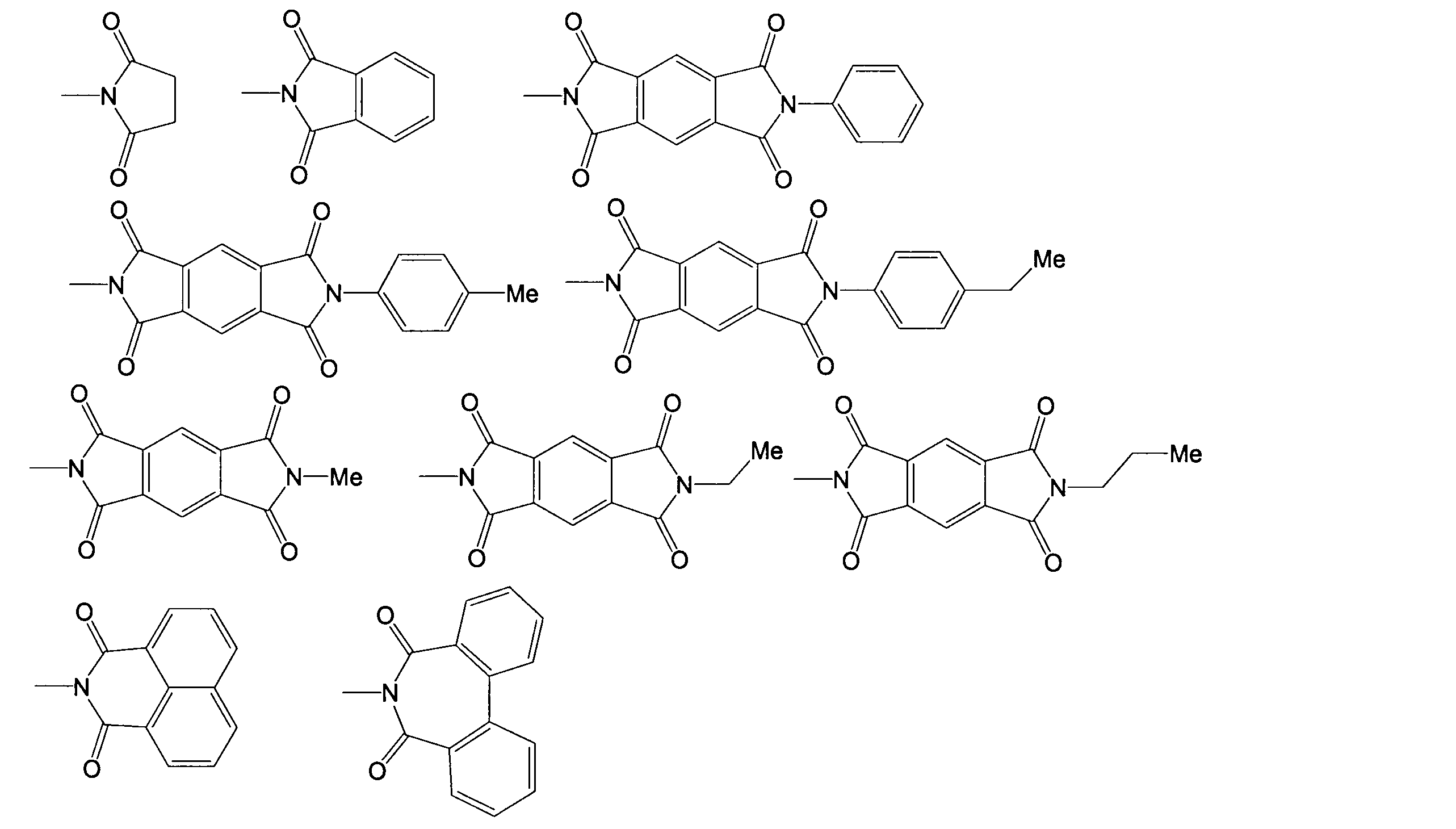
「置換オキシカルボニル基」とは、R’-O-(C=O)-で表される基を意味する。
ここで、R’は、アルキル基、アリール基、アリールアルキル基、又は1価の複素環基を表す。
ここで、R’は、アルキル基、アリール基、アリールアルキル基、又は1価の複素環基を表す。
置換オキシカルボニル基の炭素原子数は、置換基の炭素原子数を含めないで、通常2~60であり、好ましくは2~48である。
置換オキシカルボニル基の具体例としては、メトキシカルボニル基、エトキシカルボニル基、プロポキシカルボニル基、イソプロポキシカルボニル基、ブトキシカルボニル基、イソブトキシカルボニル基、tert-ブトキシカルボニル基、ペンチルオキシカルボニル基、ヘキシルオキシカルボニル基、シクロヘキシルオキシカルボニル基、ヘプチルオキシカルボニル基、オクチルオキシカルボニル基、2-エチルヘキシルオキシカルボニル基、ノニルオキシカルボニル基、デシルオキシカルボニル基、3,7-ジメチルオクチルオキシカルボニル基、ドデシルオキシカルボニル基、トリフルオロメトキシカルボニル基、ペンタフルオロエトキシカルボニル基、パーフルオロブトキシカルボニル基、パーフルオロヘキシルオキシカルボニル基、パーフルオロオクチルオキシカルボニル基、フェノキシカルボニル基、ナフトキシカルボニル基、及びピリジルオキシカルボニル基が挙げられる。
「アルケニル基」は、直鎖状、分岐状、及び環状のいずれであってもよい。直鎖状のアルケニル基の炭素原子数は、置換基の炭素原子数を含めないで、通常2~30であり、好ましくは3~20である。分岐状又は環状のアルケニル基の炭素原子数は、置換基の炭素原子数を含まないで、通常3~30であり、好ましくは4~20である。
アルケニル基は、置換基を有していてもよい。アルケニル基の具体例としては、ビニル基、1-プロペニル基、2-プロペニル基、2-ブテニル基、3-ブテニル基、3-ペンテニル基、4-ペンテニル基、1-ヘキセニル基、5-ヘキセニル基、7-オクテニル基、及び、これらの基における水素原子がアルキル基、アルキルオキシ基、アリール基、フッ素原子で置換された基が挙げられる。
「シクロアルケニル基」は、単環の基であってもよく、多環の基であってもよい。シクロアルケニル基は、置換基を有していてもよい。シクロアルケニル基の炭素原子数は、置換基の炭素原子数を含めないで、通常3~30であり、好ましくは12~19である。
シクロアルケニル基の例としては、シクロヘキセニル基などの、置換基を有しないシクロアルケニル基、及びこれらの基における水素原子が、アルキル基、アルキルオキシ基、アリール基、フッ素原子で置換された基が挙げられる。
置換基を有するシクロアルケニル基の例としては、メチルシクロヘキセニル基、及びエチルシクロヘキセニル基が挙げられる。
「アルキニル基」は、直鎖状、分岐状、及び環状のいずれであってもよい。直鎖状のアルケニル基の炭素原子数は、置換基の炭素原子数を含めないで、通常2~20であり、好ましくは3~20である。分岐状又は環状のアルケニル基の炭素原子数は、置換基の炭素原子数を含めないで、通常4~30であり、好ましくは4~20である。
アルキニル基は置換基を有していてもよい。アルキニル基の具体例としては、エチニル基、1-プロピニル基、2-プロピニル基、2-ブチニル基、3-ブチニル基、3-ペンチニル基、4-ペンチニル基、1-ヘキシニル基、5-ヘキシニル基、及び、これらの基における水素原子がアルキルオキシ基、アリール基、フッ素原子で置換された基が挙げられる。
「シクロアルキニル基」は、単環の基であってもよく、多環の基であってもよい。シクロアルキニル基は、置換基を有していてもよい。シクロアルキニル基の炭素原子数は、置換基の炭素原子数を含めないで、通常4~30であり、好ましくは12~19である。
シクロアルキニル基の例としては、シクロヘキシニル基などの置換基を有しないシクロアルキニル基、及びこれらの基における水素原子が、アルキル基、アルキルオキシ基、アリール基、フッ素原子で置換された基が挙げられる。
置換基を有するシクロアルキニル基の例としては、メチルシクロヘキシニル基、及びエチルシクロヘキシニル基が挙げられる。
「アルキルスルホニル基」は、直鎖状でもあってもよく、分岐状であってもよい。アルキルスルホニル基は、置換基を有していてもよい。アルキルスルホニル基の炭素原子数は、置換基の炭素原子数を含めないで、通常1~30である。アルキルスルホニル基の具体例としては、メチルスルホニル基、エチルスルホニル基、及びドデシルスルホニル基が挙げられる。
化学式に付されうる符合「*」は、結合手を表す。
「インク」は、塗布法に用いられる液状体を意味しており、着色した液に限定されない。また、「塗布法」は、液状物質を用いて膜(層)を形成する方法を包含し、例えば、スロットダイコート法、スリットコート法、ナイフコート法、スピンコート法、キャスティング法、マイクログラビアコート法、グラビアコート法、バーコート法、ロールコート法、ワイヤーバーコート法、ディップコート法、スプレーコート法、スクリーン印刷法、グラビア印刷法、フレキソ印刷法、オフセット印刷法、インクジェットコート法、ディスペンサー印刷法、ノズルコート法、及びキャピラリーコート法が挙げられる。
インクは、溶液であってよく、分散液、エマルション(乳濁液)、サスペンション(懸濁液)などの分散液であってもよい。
「吸収ピーク波長」とは、所定の波長範囲で測定された吸収スペクトルの吸収ピークに基づいて特定されるパラメータであり、吸収スペクトルの吸収ピークのうちの吸光度が最も大きい吸収ピークの波長をいう。
「外部量子効率」とは、EQE(External Quantum Efficiency)とも称され、光電変換素子に照射された光子の数に対して発生した電子のうち光電変換素子の外部に取り出すことができた電子の数を比率(%)で示した値をいう。
1.化合物
まず、本実施形態の化合物について説明する。本実施形態の化合物は、光電変換素子の特に活性層の半導体材料として好適に用いることができる。なお、活性層において、本実施形態の化合物が、p型半導体材料及びn型半導体材料のうちのいずれとして機能するかは、選択された化合物のHOMOのエネルギーレベルの値又はLUMOのエネルギーレベルの値から相対的に決定することができる。本実施形態の化合物は、光電変換素子の活性層において、特にn型半導体材料として好適に用いることができる。
まず、本実施形態の化合物について説明する。本実施形態の化合物は、光電変換素子の特に活性層の半導体材料として好適に用いることができる。なお、活性層において、本実施形態の化合物が、p型半導体材料及びn型半導体材料のうちのいずれとして機能するかは、選択された化合物のHOMOのエネルギーレベルの値又はLUMOのエネルギーレベルの値から相対的に決定することができる。本実施形態の化合物は、光電変換素子の活性層において、特にn型半導体材料として好適に用いることができる。
活性層に含まれるp型半導体材料のHOMO及びLUMOのエネルギーレベルの値と、n型半導体材料のHOMO及びLUMOのエネルギーレベルの値との関係は、光電変換素子(光検出素子)を機能させることができる範囲に適宜設定することができる。
本実施形態の化合物は、下記式(I)で表される化合物である。
A1―P―A2 (I)
A1―P―A2 (I)
式(I)中、
A1及びA2は、それぞれ独立して、電子求引性の1価の基であり、
Pは、下記式(1)で表される2価の基である。
A1及びA2は、それぞれ独立して、電子求引性の1価の基であり、
Pは、下記式(1)で表される2価の基である。

式(1)中、
Xは、-S-で表される基、-O-で表される基、-Se-で表される基、又は-N(R)-で表される基を表し、
Y1及びY2は、それぞれ独立して、-S-で表される基、-CR1R2-で表される基、-SiR1R2-で表される基、-NR-で表される基、-C(=O)-で表される基、-C(=O)-NR-で表される基、-NR-C(=O)-で表される基、-CR1R2-O-で表される基、-O-CR1R2-、-C(=O)-CR1R2-で表される基、又は-CR1R2-C(=O)-で表される基を表し、
Ar1及びAr2は、それぞれ独立して、置換基を有していてもよく複数の環構造がさらに縮環していてもよい芳香族炭素環又は置換基を有していてもよく複数の環構造がさらに縮環していてもよい芳香族複素環を表し、
Ar3及びAr4は、それぞれ独立して、置換基を有していてもよく複数の環構造がさらに縮環していてもよい2価の芳香族炭素環基又は置換基を有していてもよく複数の環構造が縮環していてもよい2価の芳香族複素環基を表し、
n及びmは、それぞれ独立して、0、1、2又は3を表し、
R、R1及びR2は、それぞれ独立して、
水素原子、
ハロゲン原子、
置換基を有していてもよいアルキル基、
置換基を有していてもよいシクロアルキル基、
置換基を有していてもよいアリール基、
置換基を有していてもよいアルキルオキシ基、
置換基を有していてもよいシクロアルキルオキシ基、
置換基を有していてもよいアリールオキシ基、
置換基を有していてもよいアルキルチオ基、
置換基を有していてもよいシクロアルキルチオ基、
置換基を有していてもよいアリールチオ基、
置換基を有していてもよい1価の複素環基、
置換基を有していてもよい置換アミノ基、
置換基を有していてもよいアシル基、
置換基を有していてもよいイミン残基、
置換基を有していてもよいアミド基、
置換基を有していてもよい酸イミド基、
置換基を有していてもよい置換オキシカルボニル基、
置換基を有していてもよいアルケニル基、
置換基を有していてもよいシクロアルケニル基、
置換基を有していてもよいアルキニル基、
置換基を有していてもよいシクロアルキニル基、
シアノ基、
ニトロ基、
-C(=O)-Raで表される基、又は
-SO2-Rbで表される基を表し、
Ra及びRbは、それぞれ独立して、
水素原子、
置換基を有していてもよいアルキル基、
置換基を有していてもよいアリール基、
置換基を有していてもよいアルキルオキシ基、
置換基を有していてもよいアリールオキシ基、又は
置換基を有していてもよい1価の複素環基を表し、
複数あるR、R1及びR2は、同一であっても異なっていてもよい。
本実施形態の化合物は、上記式(I)で表される非フラーレン化合物であって、電子求引性の1価の基であるA1及びA2が、式(1)で表される2価の基であるPの両末端に結合した化合物である。
以下、本実施形態の化合物を構成しうるA1、A2及びPについて具体的に説明する。
(1)A1及びA2について
本実施形態の化合物において、A1及びA2は、電子求引性の1価の基である。A1とA2とは同一の基であってもよく、当該化合物の合成をより容易にする観点から、A1及びA2は同一の基であることが好ましい。
本実施形態の化合物において、A1及びA2は、電子求引性の1価の基である。A1とA2とは同一の基であってもよく、当該化合物の合成をより容易にする観点から、A1及びA2は同一の基であることが好ましい。
A1及びA2の例としては、-CH=C(-CN)2で表される基、及び下記式(a-1)~式(a-9)で表される基が挙げられる。
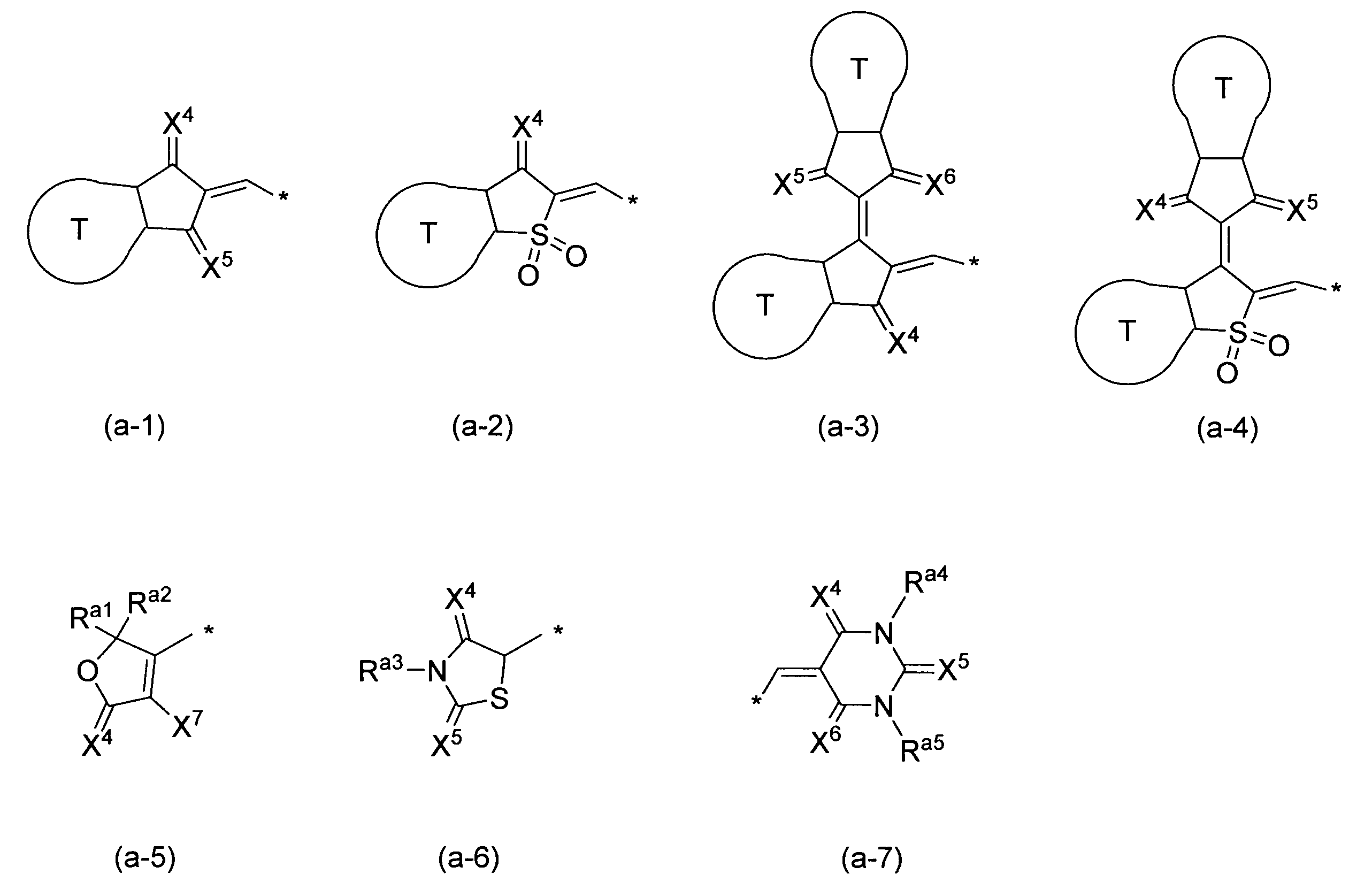
式(a-1)~式(a-7)中、
Tは、置換基を有していてもよい炭素環、又は置換基を有していてもよい複素環を表す。炭素環及び複素環は、単環であってもよく、縮合環であってもよい。これらの環が置換基を複数有する場合、複数ある置換基は、同一であっても異なっていてもよい。
Tは、置換基を有していてもよい炭素環、又は置換基を有していてもよい複素環を表す。炭素環及び複素環は、単環であってもよく、縮合環であってもよい。これらの環が置換基を複数有する場合、複数ある置換基は、同一であっても異なっていてもよい。
Tで表される置換基を有していてもよい炭素環の例としては、芳香族炭素環が挙げられ、好ましくは芳香族炭素環である。Tで表される置換基を有していてもよい炭素環の具体例としては、ベンゼン環、ナフタレン環、アントラセン環、テトラセン環、ペンタセン環、ピレン環、及びフェナントレン環が挙げられ、好ましくはベンゼン環、ナフタレン環、及びフェナントレン環であり、より好ましくはベンゼン環及びナフタレン環であり、さらに好ましくはベンゼン環である。これらの環は、置換基を有していてもよい。
Tで表される置換基を有していてもよい複素環の例としては、芳香族複素環が挙げられ、好ましくは芳香族炭素環である。Tで表される置換基を有していてもよい複素環の具体例としては、ピリジン環、ピリダジン環、ピリミジン環、ピラジン環、ピロール環、フラン環、チオフェン環、イミダゾール環、オキサゾール環、チアゾール環、及びチエノチオフェン環が挙げられ、好ましくはチオフェン環、及びピリジン環、ピラジン環、チアゾール環、及びチエノチオフェン環であり、より好ましくはチオフェン環である。これらの環は、置換基を有していてもよい。
Tで表される炭素環又は複素環が有しうる置換基の例としては、ハロゲン原子、アルキル基、アルキルオキシ基、アリール基、シアノ基及び1価の複素環基が挙げられ、好ましくはフッ素原子、塩素原子、炭素原子数1~6のアルキルオキシ基及び/又は炭素原子数1~6のアルキル基である。
X4、X5、及びX6は、それぞれ独立して、酸素原子、硫黄原子、アルキリデン基、又は=C(-CN)2で表される基を表し、好ましくは、酸素原子、硫黄原子、又は=C(-CN)2で表される基である。
X7は、水素原子又はハロゲン原子、シアノ基、置換基を有していてもよいアルキル基、置換基を有していてもよいアルキルオキシ基、置換基を有していてもよいアリール基又は1価の複素環基を表す。X7は、好ましくはシアノ基である。
Ra1、Ra2、Ra3、Ra4、及びRa5は、それぞれ独立して、水素原子、置換基を有していてもよいアルキル基、ハロゲン原子、置換基を有していてもよいアルキルオキシ基、置換基を有していてもよいアリール基又は1価の複素環基を表し、好ましくは、置換基を有していてもよいアルキル基又は置換基を有していてもよいアリール基である。
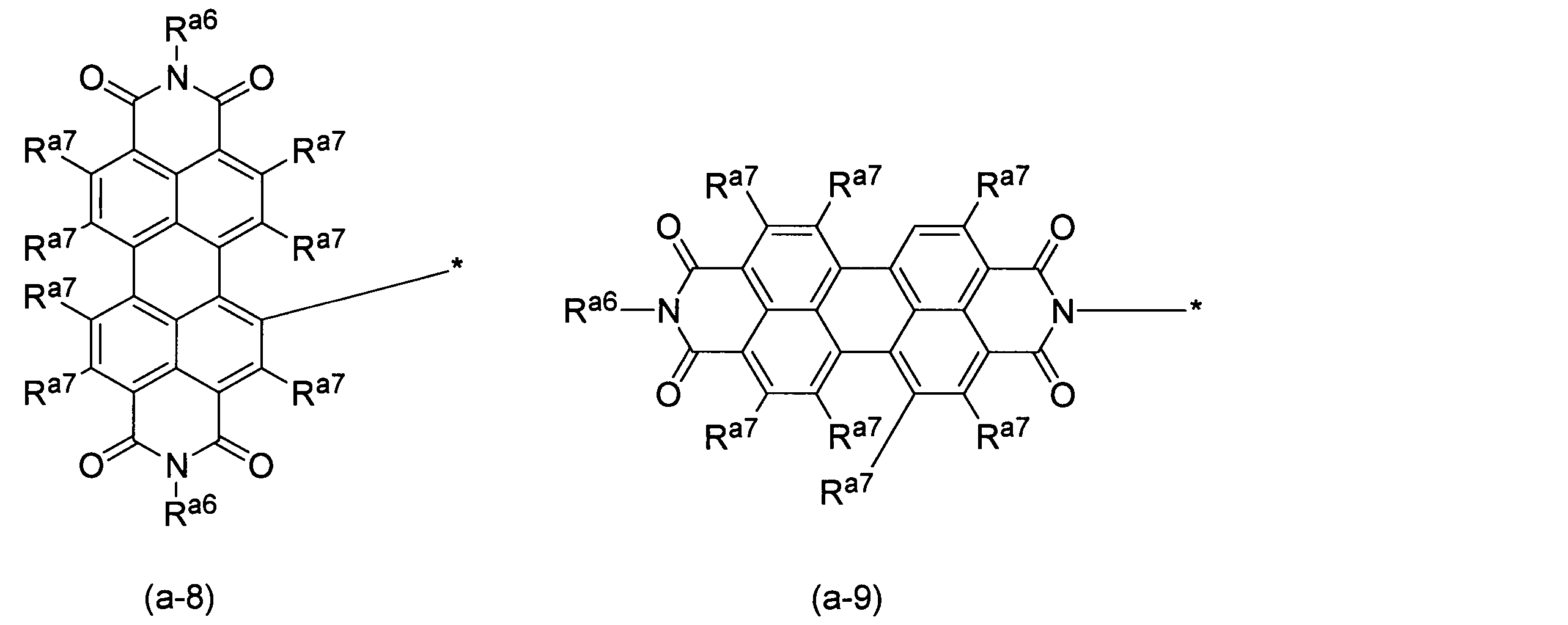
式(a-8)及び式(a-9)中、
Ra6及びRa7は、それぞれ独立して、水素原子、ハロゲン原子、置換基を有していてもよいアルキル基、置換基を有していてもよいシクロアルキル基、置換基を有していてもよいアルキルオキシ基、置換基を有していてもよいシクロアルキルオキシ基、置換基を有していてもよい1価の芳香族炭素環基、又は置換基を有していてもよい1価の芳香族複素環基を表し、複数あるRa6及びRa7は、互いに同一であっても異なっていてもよい。
Ra6及びRa7は、それぞれ独立して、水素原子、ハロゲン原子、置換基を有していてもよいアルキル基、置換基を有していてもよいシクロアルキル基、置換基を有していてもよいアルキルオキシ基、置換基を有していてもよいシクロアルキルオキシ基、置換基を有していてもよい1価の芳香族炭素環基、又は置換基を有していてもよい1価の芳香族複素環基を表し、複数あるRa6及びRa7は、互いに同一であっても異なっていてもよい。
A1及びA2で表される電子求引性の1価の基の具体例としては、下記式(a-1-1)~式(a-1-4)、並びに式(a-5-1)、式(a-6-1)、式(a-6-2)及び式(a-7-1)で表される基が挙げられる。
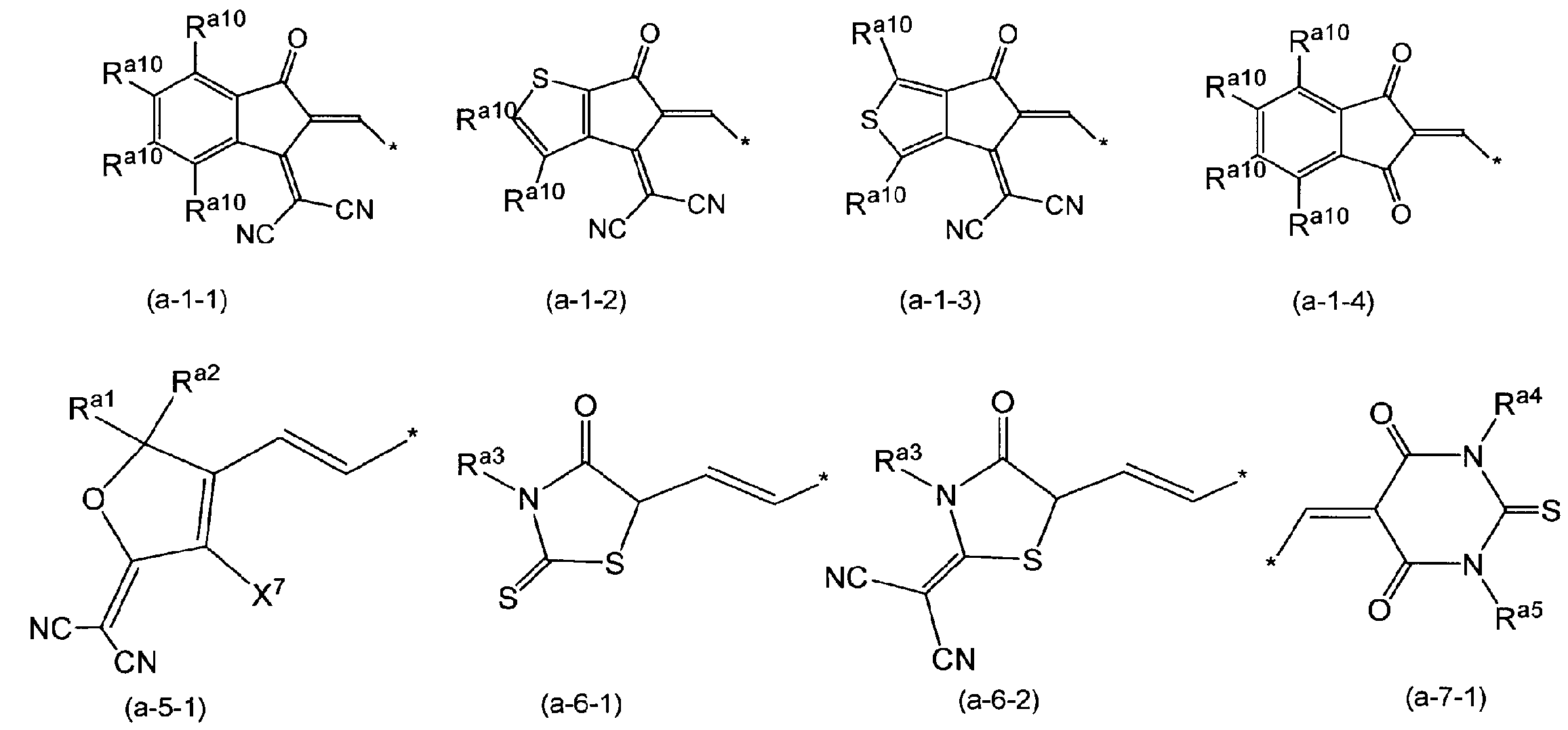
式(a-1-1)~式(a-1-4)、並びに式(a-5-1)、式(a-6-1)、式(a-6-2)及び式(a-7-1)中、
複数あるRa10は、それぞれ独立して、水素原子又は置換基を表し、
Ra1、Ra2、Ra3、Ra4、及びRa5は、それぞれ独立して、前記と同義である。
複数あるRa10は、それぞれ独立して、水素原子又は置換基を表し、
Ra1、Ra2、Ra3、Ra4、及びRa5は、それぞれ独立して、前記と同義である。
Ra10は、好ましくは水素原子、ハロゲン原子、アルキルオキシ基、シアノ基又はアルキル基である。Ra1、Ra2、Ra3、Ra4、及びRa5は、好ましくは置換基を有していてもよいアルキル基又は置換基を有していてもよいアリール基である。
A1及びA2は、それぞれ独立して、シアノ基、カルボニル基及びチオカルボニル基からなる群から選択される1種以上を含む電子求引性の基であることが好ましい。
A1及びA2で表される電子求引性の1価の基の好ましい例としては、下記式で表される基が挙げられる。
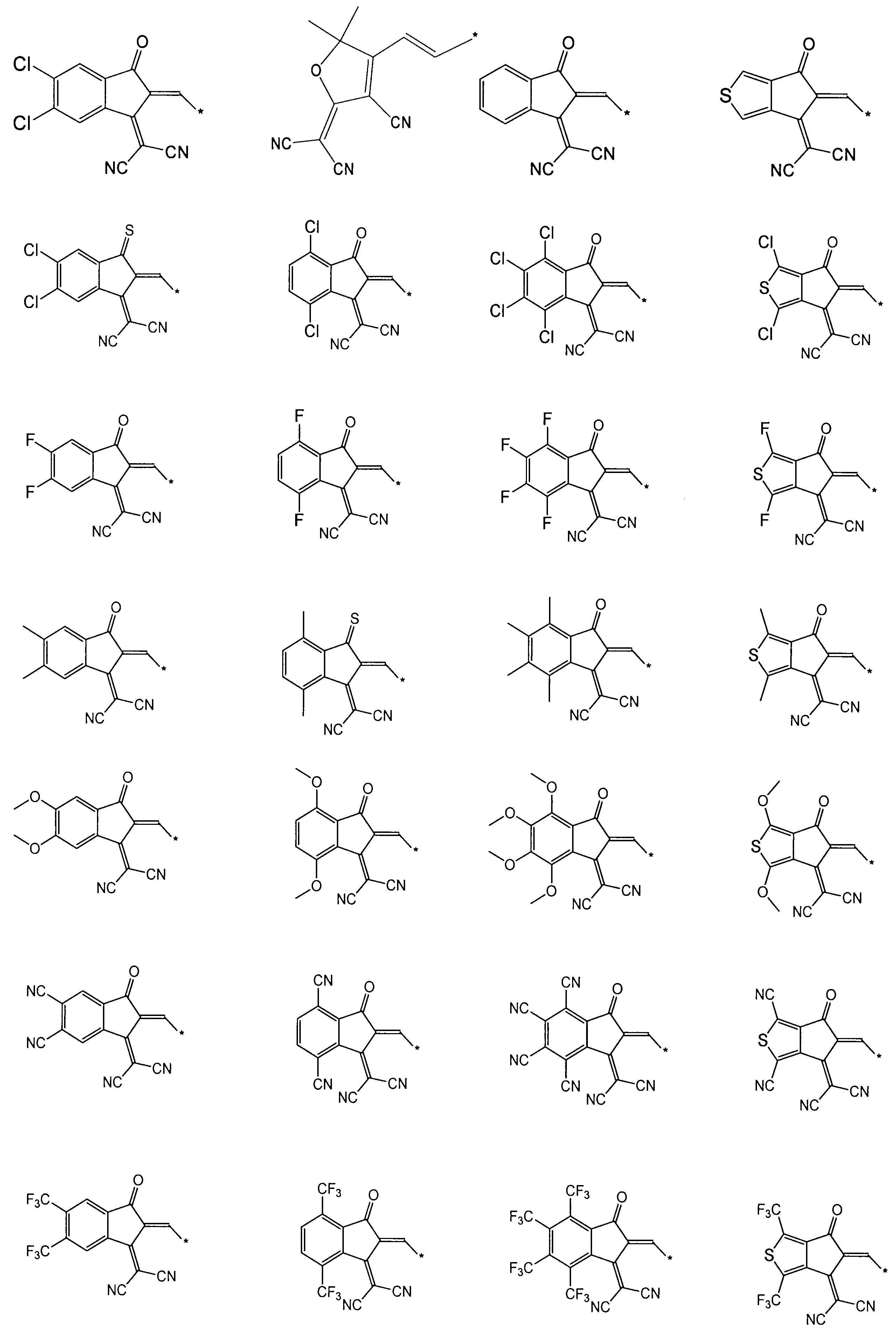

(2)Pについて
前記式(I)で表される化合物におけるPは、下記式(1)で表される2価の基である。Pは、互いにπ結合している一対以上の原子を含んでおり、π電子雲がPの全体にわたって広がっている2価の基である。
前記式(I)で表される化合物におけるPは、下記式(1)で表される2価の基である。Pは、互いにπ結合している一対以上の原子を含んでおり、π電子雲がPの全体にわたって広がっている2価の基である。
よって、前記式(I)で表される化合物は、A1、A2及びPの全体にわたってπ電子雲が広がっている化合物であることが好ましい。

式(1)中、Xは、-S-で表される基、-O-で表される基、-Se-で表される基、又は-NR-で表される基を表す。
Xは、光電変換素子(光検出素子)における暗電流をより効果的に低減させる観点から、-S-で表される基、又は-O-で表される基であることが好ましく、-S-で表される基であることがより好ましい。
ここで、Rは、水素原子、ハロゲン原子、置換基を有していてもよいアルキル基、置換基を有していてもよいシクロアルキル基、置換基を有していてもよいアリール基、置換基を有していてもよいアルキルオキシ基、置換基を有していてもよいシクロアルキルオキシ基、置換基を有していてもよいアリールオキシ基、置換基を有していてもよいアルキルチオ基、置換基を有していてもよいシクロアルキルチオ基、置換基を有していてもよいアリールチオ基、置換基を有していてもよい1価の複素環基、置換基を有していてもよい置換アミノ基、置換基を有していてもよいアシル基、置換基を有していてもよいイミン残基、置換基を有していてもよいアミド基、置換基を有していてもよい酸イミド基、置換基を有していてもよい置換オキシカルボニル基、置換基を有していてもよいアルケニル基、置換基を有していてもよいシクロアルケニル基、置換基を有していてもよいアルキニル基、置換基を有していてもよいシクロアルキニル基、シアノ基、ニトロ基、-C(=O)-Raで表される基、又は-SO2-Rbで表される基を表し、Ra及びRbは、それぞれ独立して、水素原子、置換基を有していてもよいアルキル基、置換基を有していてもよいアリール基、置換基を有していてもよいアルキルオキシ基、置換基を有していてもよいアリールオキシ基、又は置換基を有していてもよい1価の複素環基を表し、複数あるRは、同一であっても異なっていてもよい。Rは、置換基を有していてもよいアルキル基、置換基を有していてもよいアリール基置換基を有していてもよい1価の複素環基であることが好ましく、置換基を有していてもよいアルキル基であることがより好ましい。
式(1)中、Y1及びY2は、それぞれ独立して、-S-で表される基、-CR1R2-で表される基、-SiR1R2-で表される基、-NR-で表される基、-C(=O)-で表される基、-C(=O)-NR-で表される基、-NR-C(=O)-で表される基、-CR1R2-O-で表される基、-O-CR1R2-、-C(=O)-CR1R2-で表される基、又は-CR1R2-C(=O)-を表す。
ここで、R1及びR2は、それぞれ独立して、既に説明したRと同義であり、また好適例についてもRと同様であるので、これらの詳細な説明については省略する。
Ar1及びAr2は、それぞれ独立して、置換基を有していてもよく複数の環構造がさらに縮環していてもよい芳香族炭素環又は置換基を有していてもよく複数の環構造がさらに縮環していてもよい芳香族複素環である。
Ar1及びAr2は、それぞれ独立して、置換基を有していてもよいチオフェン環を含む環構造であることが好ましく、置換基を有していてもよいチオフェン環のみから構成されていてもよい。
Ar1及びAr2で表される芳香族炭素環の炭素原子数は、置換基の炭素原子数を含めないで通常6~60であり、好ましくは6~20である。置換基を含めた芳香族炭素環の炭素原子数は、通常6~100である。
Ar1及びAr2で表される芳香族炭素環の例としては、下記式(001)から式(010)で表される芳香族炭素環が挙げられる。これらの芳香族炭素環はさらに置換基を有していてもよい。

上記式(001)から式(010)で表されるAr1及びAr2で表される芳香族炭素環の好ましい具体例としては、下記式で表される芳香族炭素環が挙げられる。

Ar1及びAr2で表される芳香族複素環の炭素原子数は、通常2~60であり、好ましくは4~60であり、より好ましくは4~20である。
Ar1及びAr2で表される芳香族複素環が有していてもよい置換基の例としては、ハロゲン原子、置換基を有していてもよいアルキル基、置換基を有していてもよいアリール基、置換基を有していてもよいアルキルオキシ基、置換基を有していてもよいアリールオキシ基、置換基を有していてもよいアルキルチオ基、置換基を有していてもよいアリールチオ基、置換基を有していてもよい1価の複素環基、置換基を有していてもよい置換アミノ基、置換基を有していてもよいアシル基、置換基を有していてもよいイミン残基、置換基を有していてもよいアミド基、置換基を有していてもよい酸イミド基、置換基を有していてもよい置換オキシカルボニル基、置換基を有していてもよいアルケニル基、置換基を有していてもよいアルキニル基、シアノ基、及びニトロ基が挙げられる。
Ar1及びAr2で表される芳香族複素環の具体例としては、下記式(101)~式(125)で表される基が挙げられる。これらの芳香族複素環はさらに置換基を有していてもよい。
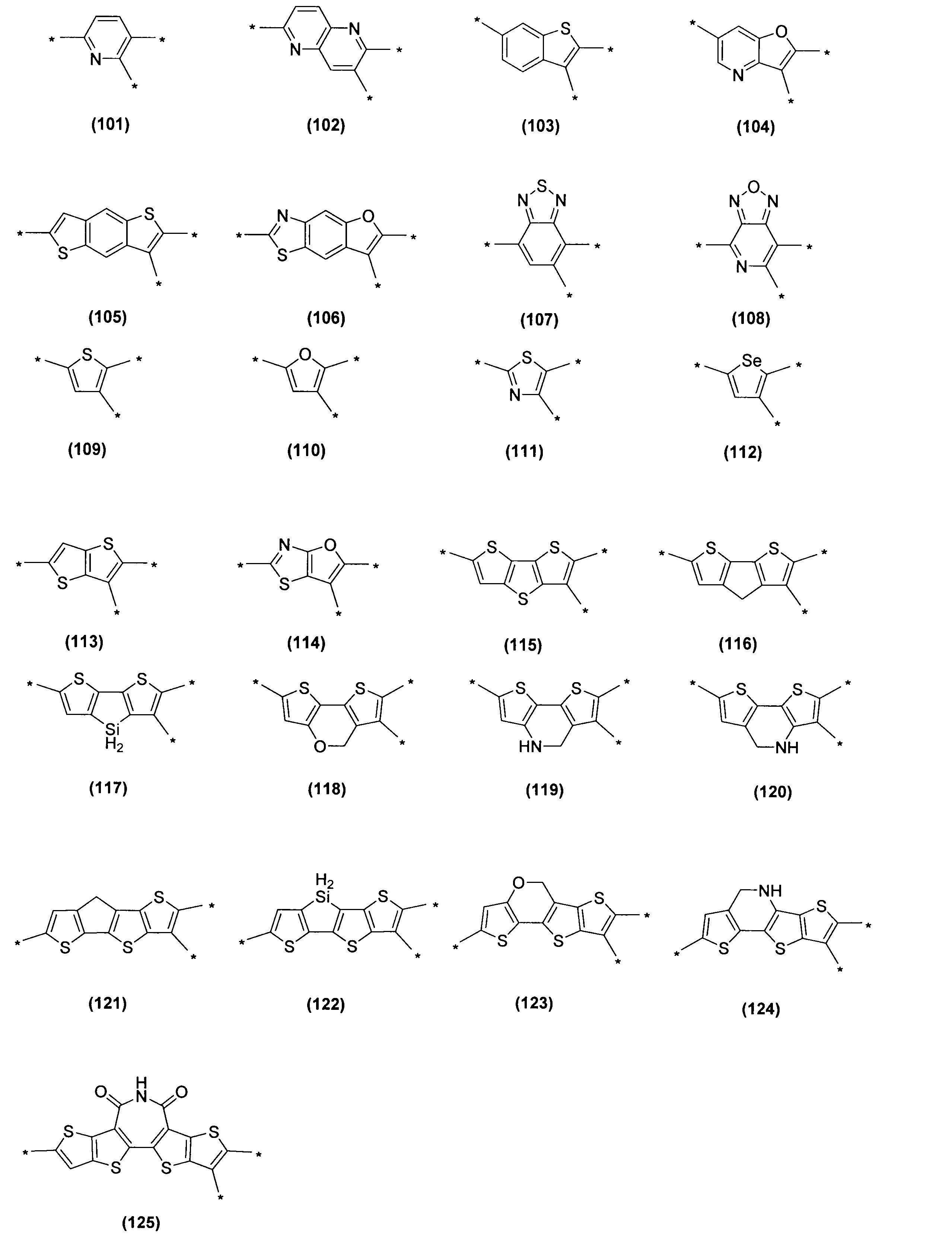
Ar1及びAr2は、置換基を有していてもよいチオフェン環または下記式で表される環構造であることが好ましい。

前記式中、Y5は、-S-で表される基、-CR1R2-で表される基、-SiR1R2-で表される基、-NR-で表される基、-C(=O)-で表される基、-C(=O)-NR-で表される基、-NR-C(=O)-で表される基、-CR1R2-O-で表される基、-O-CR1R2-、-C(=O)-CR1R2-で表される基、又は-CR1R2-C(=O)-を表す。Y5が複数ある場合、複数あるY5は同一であっても異なっていてもよい。
前記式中、R、R1及びR2は、前記定義のとおりである。
前記式中、R、R1及びR2は、前記定義のとおりである。
Ar1及びAr2の好ましい具体例としては、下記式で表される環構造が挙げられる。

式(1)で表される2価の基は、Y1及びY2が、-NR-で表される基、-S-で表される基、又は-O-CR1R2-で表される基であることが好ましく、-NR-で表される基、又は-S-で表される基であることがより好ましい。
前記式(1)で表される2価の基は、Y1及びY2が-NR-で表される基であるか、又はPが下記式(2)で表される2価の基であることが好ましい。

式(2)中、
Y3及びY4は、それぞれ独立して、-S-で表される基、-CR1R2-で表される基、-SiR1R2-で表される基、-NR-で表される基、-C(=O)-で表される基、-C(=O)-NR-で表される基、-CR1R2-O-で表される基、-O-CR1R2-で表される基、-C(=O)-CR1R2-で表される基、又は-CR1R2-C(=O)-で表される基を表し、
X、R、R1及びR2の好ましい例等は、前記式(1)において既に説明したとおりである。
Y3及びY4は、それぞれ独立して、-S-で表される基、-CR1R2-で表される基、-SiR1R2-で表される基、-NR-で表される基、-C(=O)-で表される基、-C(=O)-NR-で表される基、-CR1R2-O-で表される基、-O-CR1R2-で表される基、-C(=O)-CR1R2-で表される基、又は-CR1R2-C(=O)-で表される基を表し、
X、R、R1及びR2の好ましい例等は、前記式(1)において既に説明したとおりである。
Y1及びY2が-NR-で表される基である式(1)で表される2価の基の好ましい例としては、下記式(1-1)で表される基が挙げられる。

式(1-1)中、
X、R、Ar3、Ar4、m及びnは、前記定義のとおりである。
X、R、Ar3、Ar4、m及びnは、前記定義のとおりである。
上記式(1-1)で表される2価の基のより具体的な好ましい例としては、下記式で表される2価の基が挙げられる。
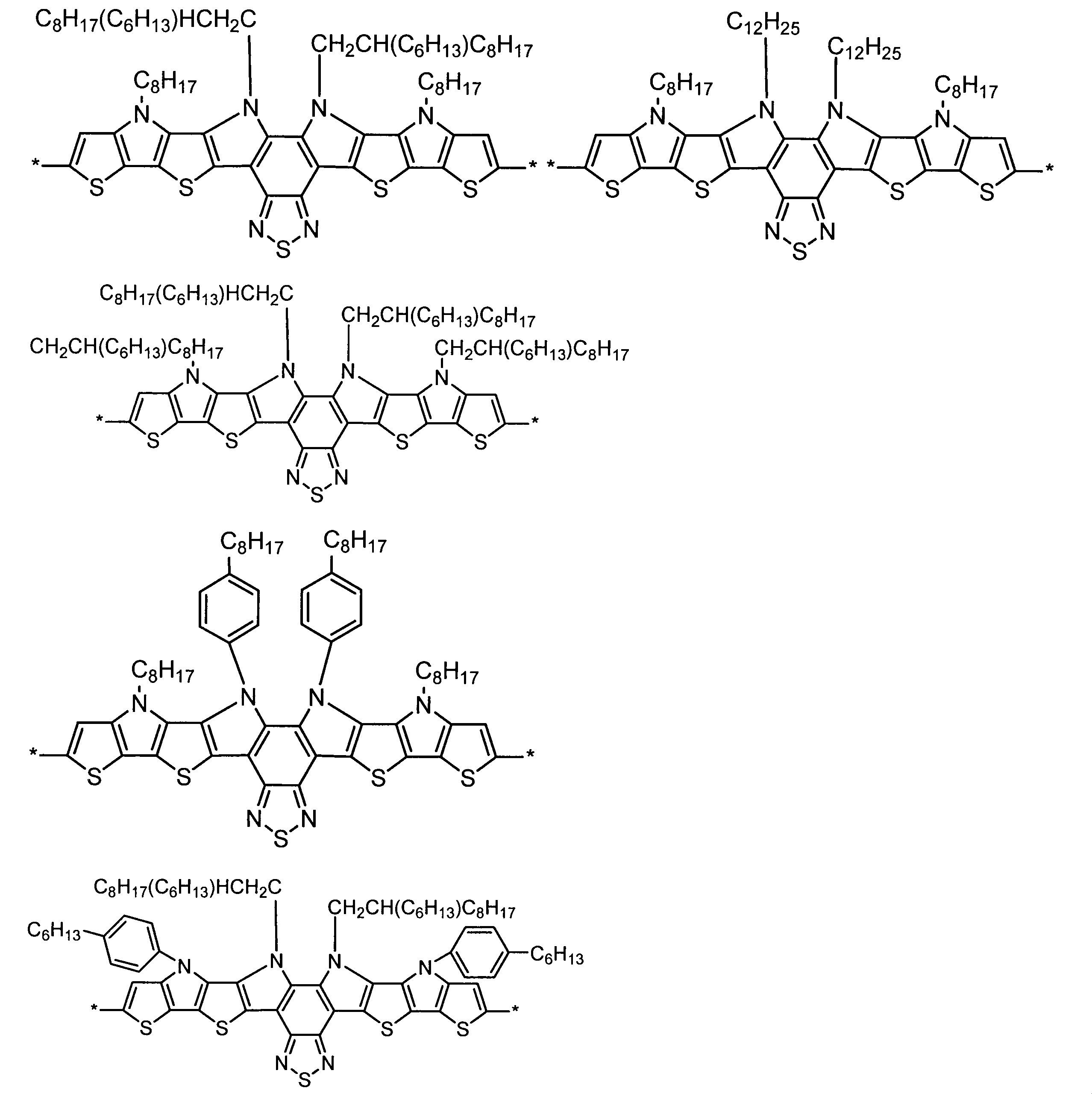

また、式(1)で表される2価の基の好ましい例としては、下記式(1-2)で表される基が挙げられる。

式(1-2)中、
Y3及びY4は、それぞれ独立して、-S-で表される基、-CR1R2-で表される基、-SiR1R2-で表される基、-NR-で表される基、-C(=O)-で表される基、-C(=O)-NR-で表される基、-CR1R2-O-で表される基、-O-CR1R2-、-C(=O)-CR1R2-で表される基、又は-CR1R2-CO-を表し、
X、R、R1、R2、Ar3、Ar4、m及びnは、前記定義のとおりである。
Y3及びY4は、それぞれ独立して、-S-で表される基、-CR1R2-で表される基、-SiR1R2-で表される基、-NR-で表される基、-C(=O)-で表される基、-C(=O)-NR-で表される基、-CR1R2-O-で表される基、-O-CR1R2-、-C(=O)-CR1R2-で表される基、又は-CR1R2-CO-を表し、
X、R、R1、R2、Ar3、Ar4、m及びnは、前記定義のとおりである。
前記式(1-2)で表される2価の基の好ましい例としては、下記式(1-2a)、式(1-2b)及び式(1-2c)で表される構造を有する基が挙げられる。
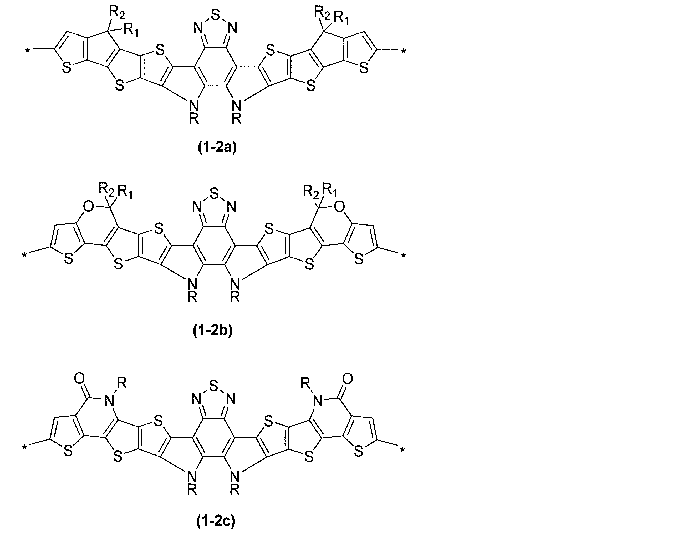
式(1-2a)、式(1-2b)及び式(1-2c)中、Rは前記定義のとおりである。
前記式(1-2a)、式(1-2b)及び式(1-2c)で表される構造を有する2価の基の好ましい具体例としては、下記式で表される2価の基が挙げられる。
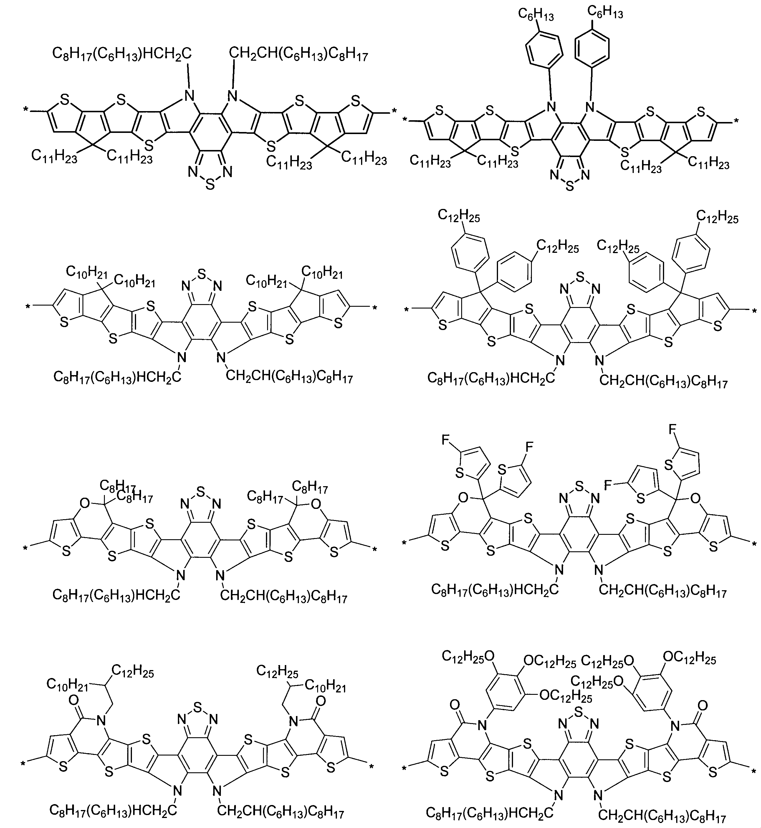
さらに、式(1)で表される2価の基の好ましい例としては、下記式(1-3)で表される基が挙げられる。

式(1-3)中、
X、Y3、Y4、R、R1及びR2は、前記定義のとおりである。
X、Y3、Y4、R、R1及びR2は、前記定義のとおりである。
前記式(1-3)で表される2価の基の好ましい例としては、下記式で表される基が挙げられる。
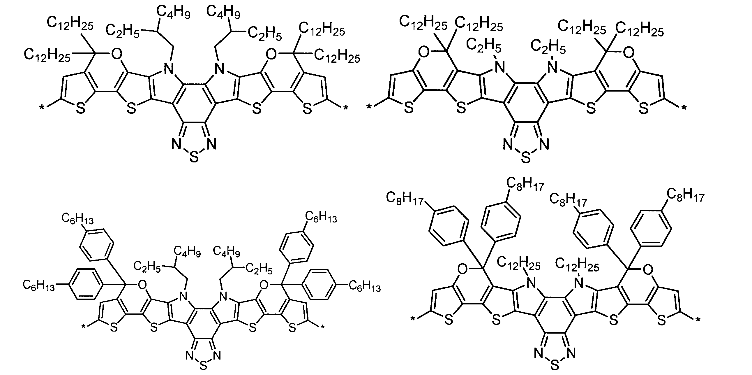
式(1)中、Ar3及びAr4は、それぞれ独立して、置換基を有していてもよく複数の環構造が縮環していてもよい2価の芳香族炭素環基、置換基を有していてもよく複数の環構造が縮環していてもよい2価の芳香族複素環基、置換基を有していてもよい-CH=CH-で表される基及び-C≡C-で表される基からなる群から選択される基である。Ar3及びAr4がそれぞれ複数ある場合には、複数あるAr3及び複数あるAr4は、同一であっても異なっていてもよい。
Ar3及びAr4は、チオフェン環を含み、置換基を有していてもよく複数の環構造が縮環していてもよい2価の芳香族複素環基であることが好ましい。
式(1)中、Ar3及びAr4である2価の芳香族炭素環基(アリーレン基)とは、具体的には、置換基を有していてもよい芳香族炭化水素から、水素原子を2個除いた残りの原子団を意味している。ここで、芳香族炭化水素には、複数の環構造が縮環している縮合環を有する化合物も含まれる。
Ar3及びAr4で表される2価の芳香族炭素環基の炭素原子数は、置換基の炭素原子数を含めないで通常6~60であり、好ましくは6~20である。置換基を含めた芳香族炭素環基の炭素原子数は、通常6~100である。
Ar3及びAr4で表される2価の芳香族炭素環基基の例としては、下記式(201)から式(210)で表される2価の芳香族炭素環基が挙げられる。これらの基はさらに置換基を有していてもよい。
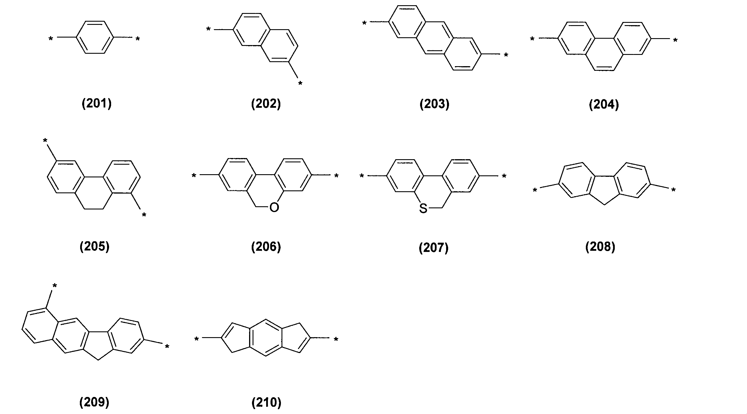
Ar3及びAr4で表される2価の芳香族炭化水素基は、下記式で表される2価の芳香族炭素環基であることが好ましい。

Ar3及びAr4で表される2価の芳香族複素環基の炭素原子数は、通常2~60であり、好ましくは4~60であり、より好ましくは4~20である。
Ar3及びAr4で表される2価の芳香族複素環基が有していてもよい置換基の例としては、ハロゲン原子、置換基を有していてもよいアルキル基、置換基を有していてもよいアリール基、置換基を有していてもよいアルキルオキシ基、置換基を有していてもよいアリールオキシ基、置換基を有していてもよいアルキルチオ基、置換基を有していてもよいアリールチオ基、置換基を有していてもよい1価の複素環基、置換基を有していてもよい置換アミノ基、置換基を有していてもよいアシル基、置換基を有していてもよいイミン残基、置換基を有していてもよいアミド基、置換基を有していてもよい酸イミド基、置換基を有していてもよい置換オキシカルボニル基、置換基を有していてもよいアルケニル基、置換基を有していてもよいアルキニル基、シアノ基、及びニトロ基が挙げられる。
Ar3及びAr4で表される2価の芳香族複素環基の具体例としては、下記式(301)から式(343)で表される2価の芳香族複素環基が挙げられる。これらの基はさらに置換基を有していてもよい。
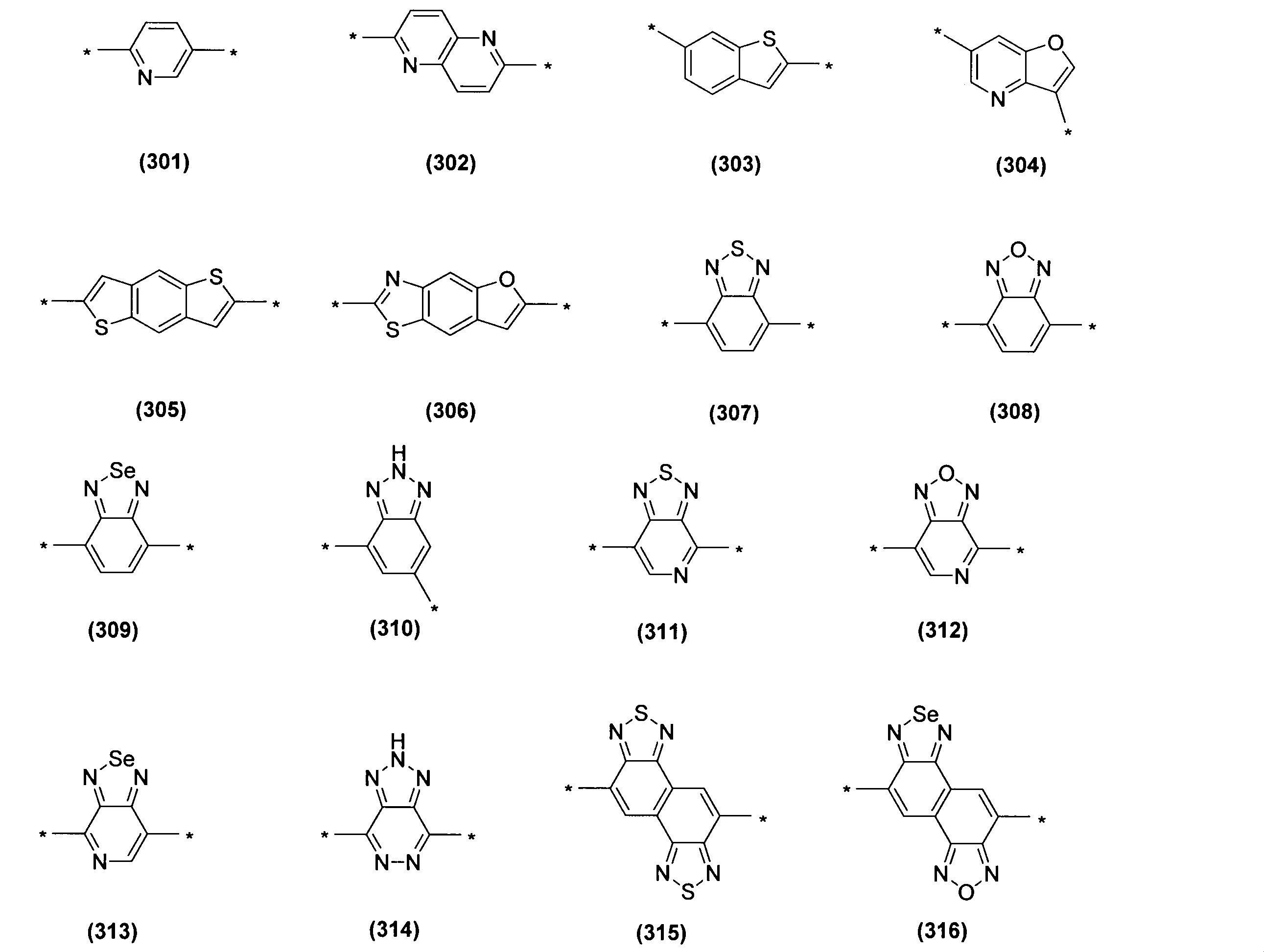

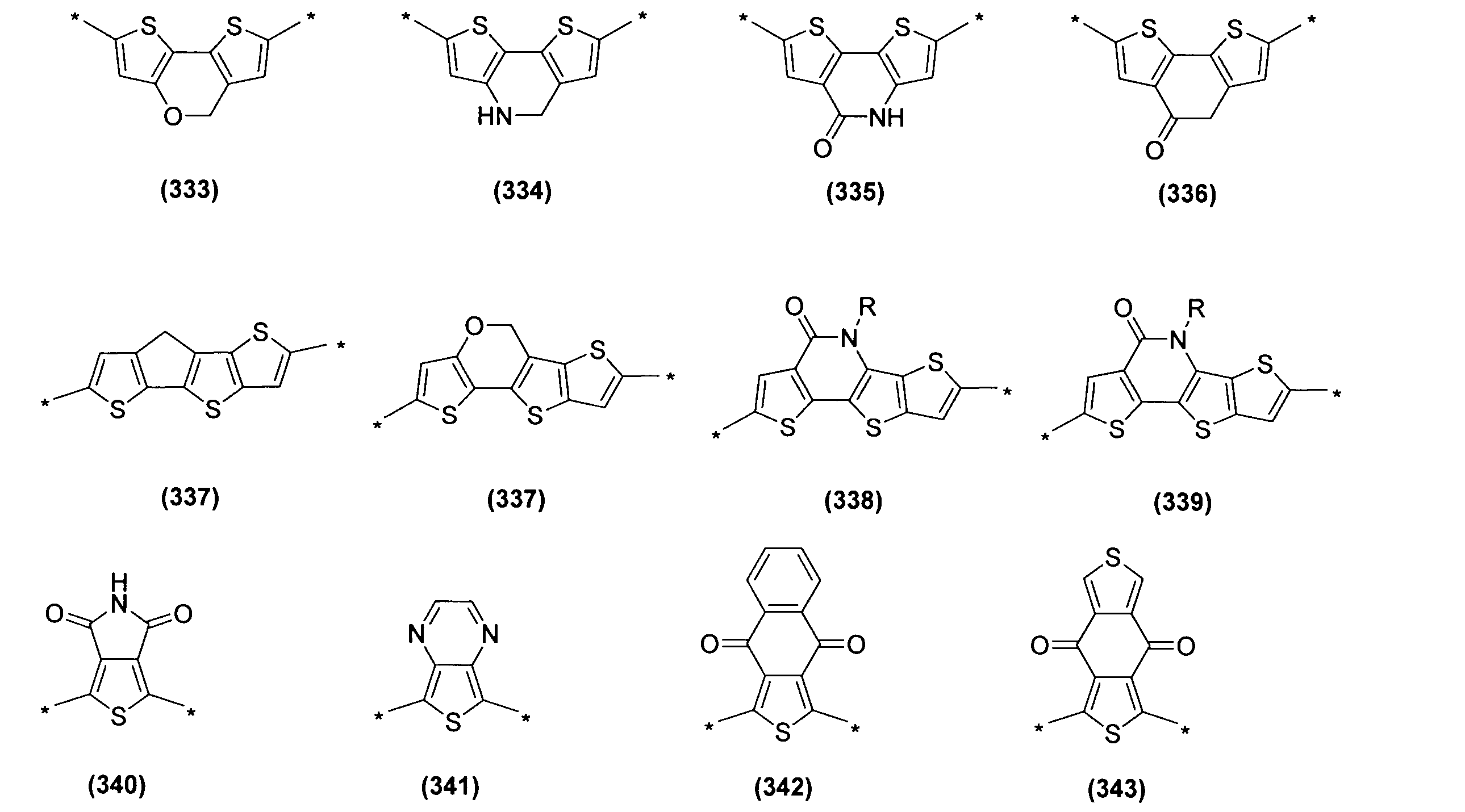
Ar3及びAr4で表される2価の芳香族複素環基としては、下記式で表される2価の芳香族複素環基が好ましい。これらの基はさらに置換基を有していてもよい。

上記式で表されるAr3及びAr4で表される2価の芳香族複素環基の好ましい具体例としては、下記式で表される2価の基が挙げられる。
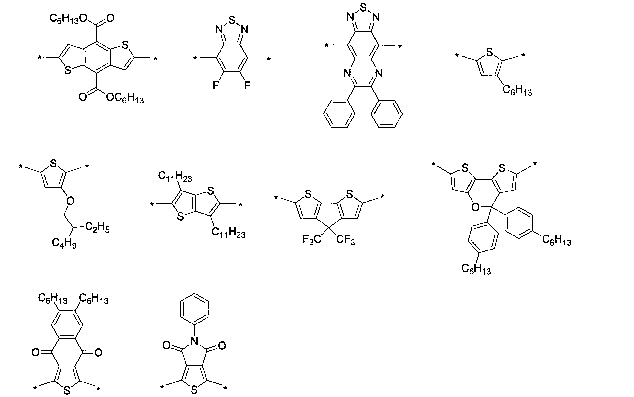
前記式(1)中、n及びmは、それぞれ独立して、0、1、2又は3であり、合成をより容易にする観点からは、n及びmは、それぞれ独立して、0又は1であることが好ましい。よって、本実施形態の化合物は、Ar3及びAr4のうちのいずれか一方又は双方を含んでいなくともよい。
本実施形態の式(I)で表される化合物の好適な具体例としては、下記式で表される化合物が挙げられる。

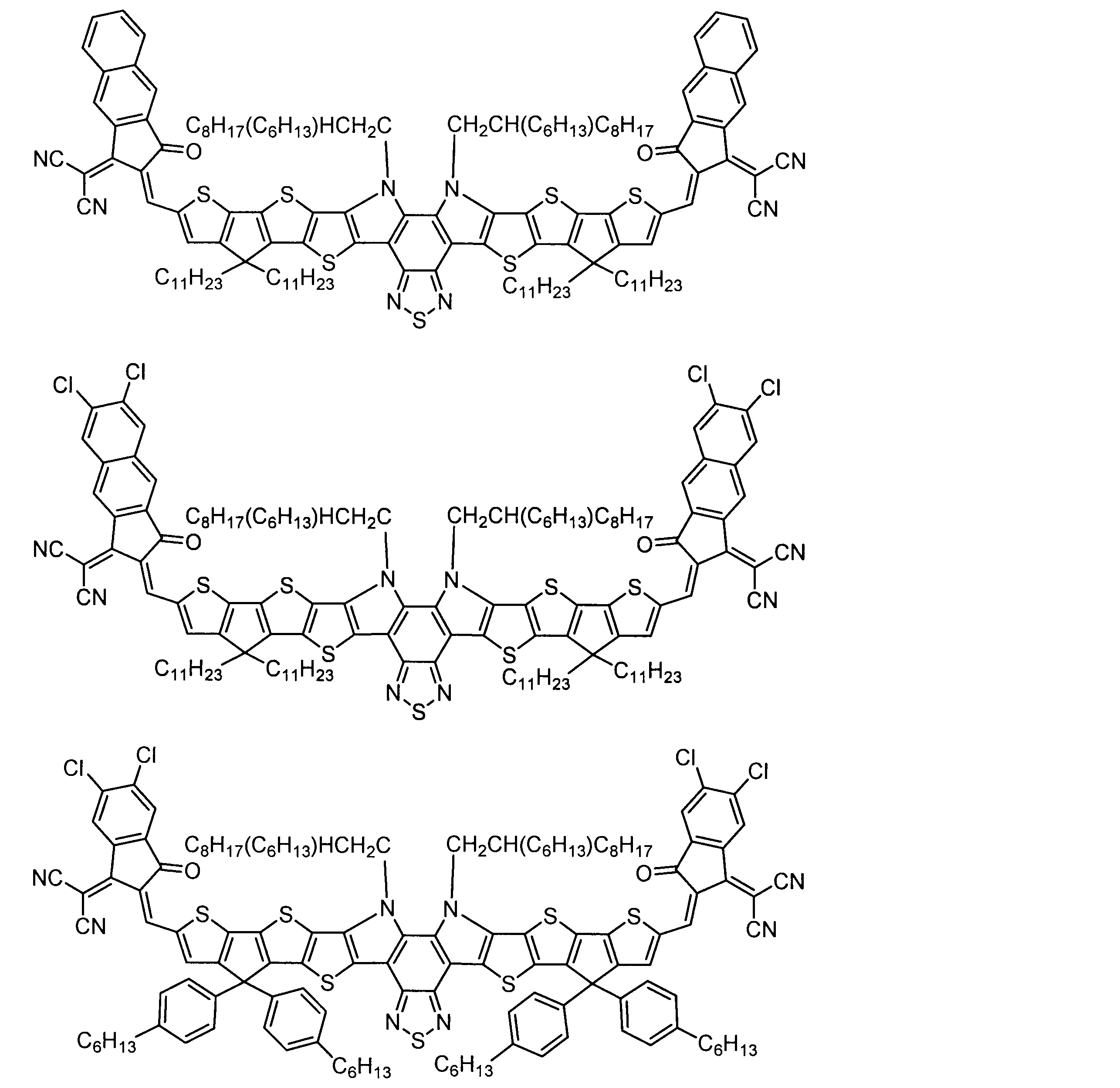
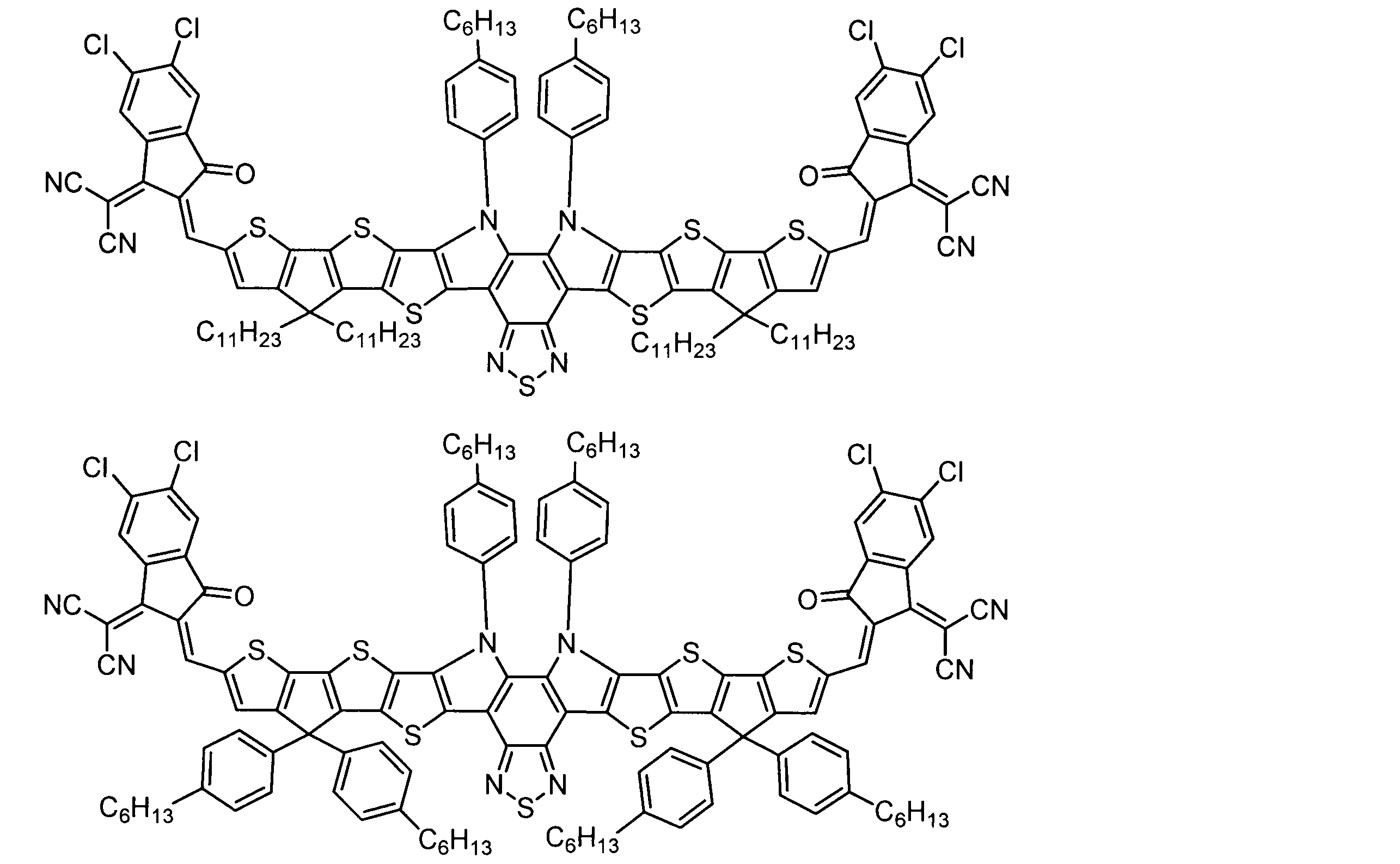
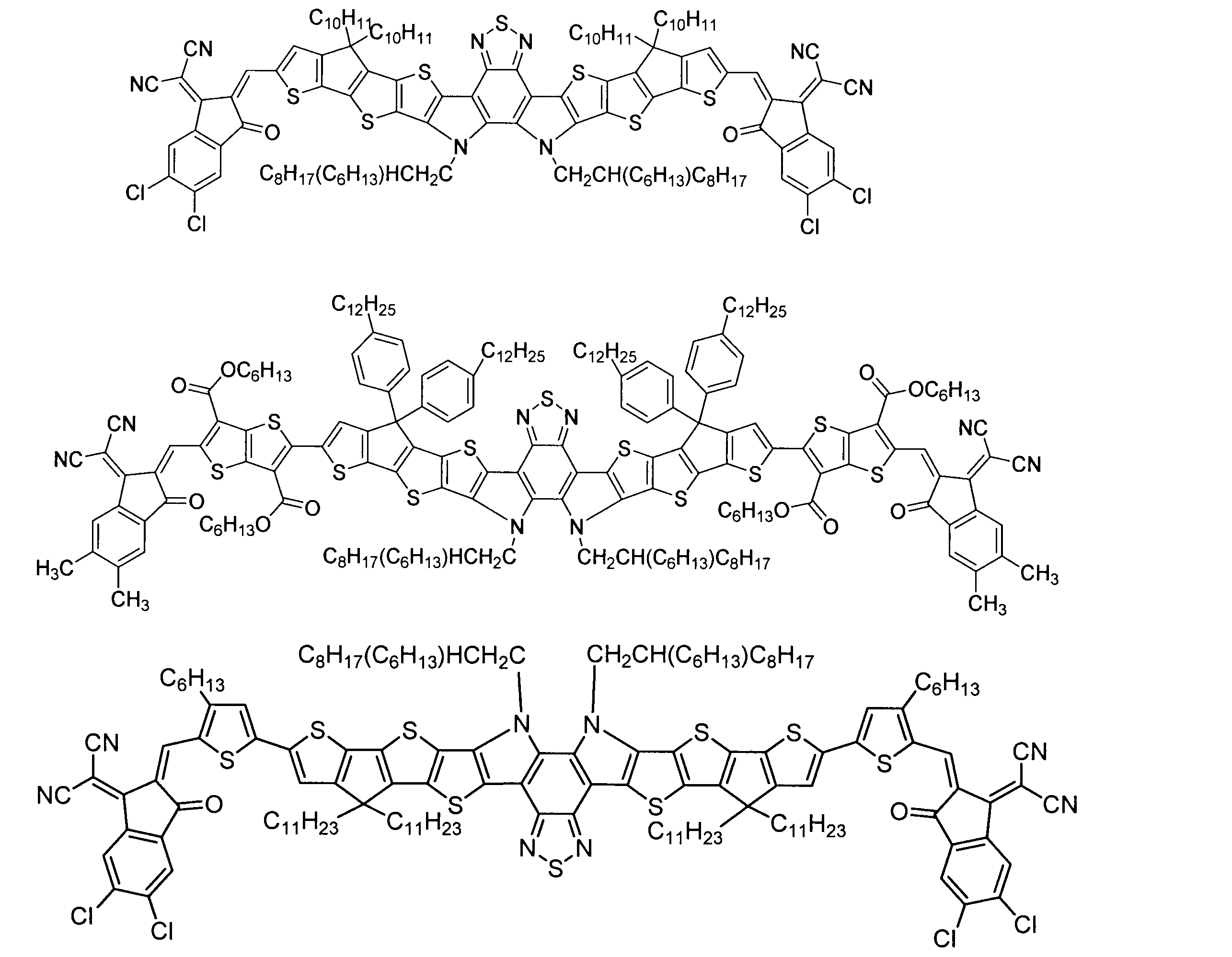

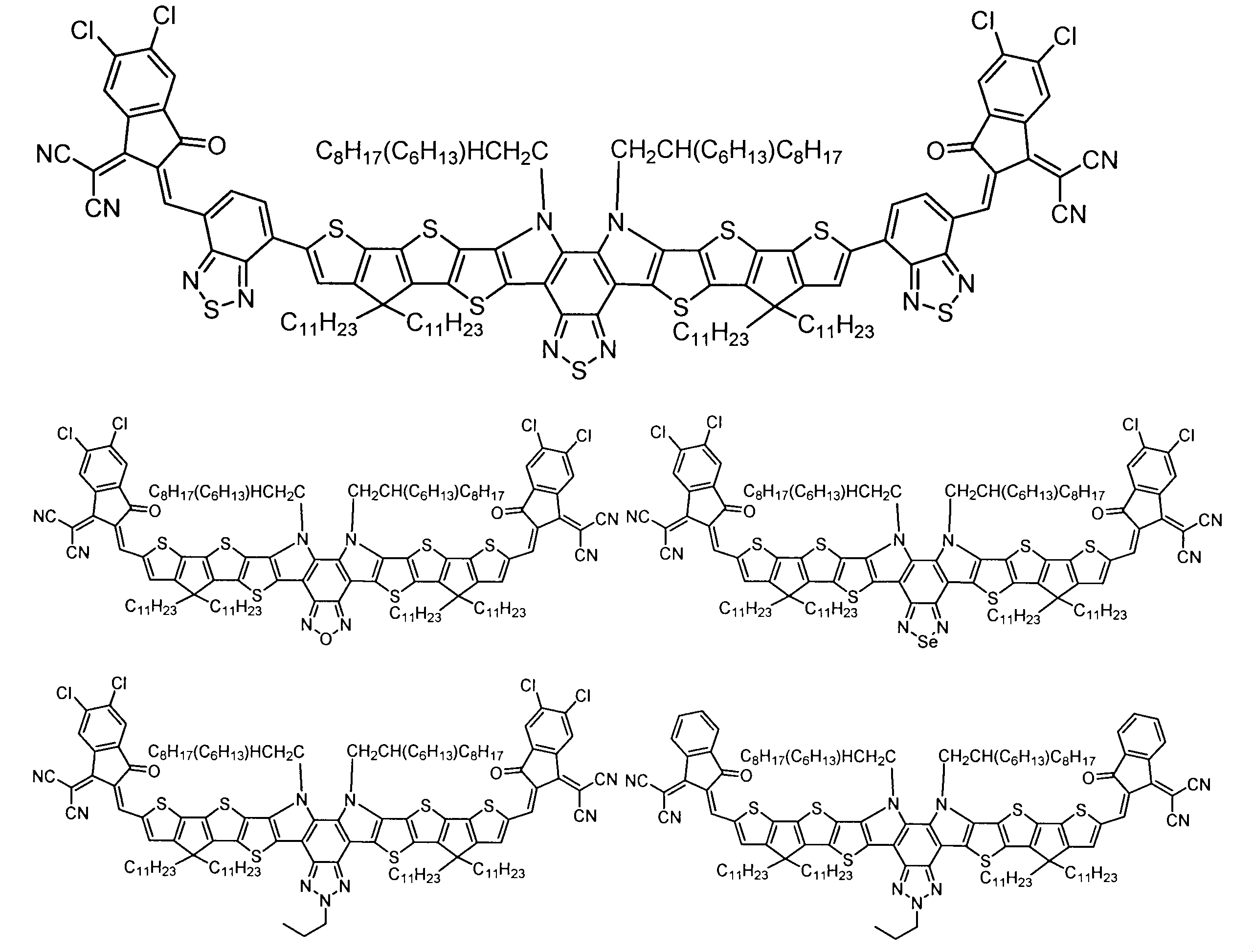
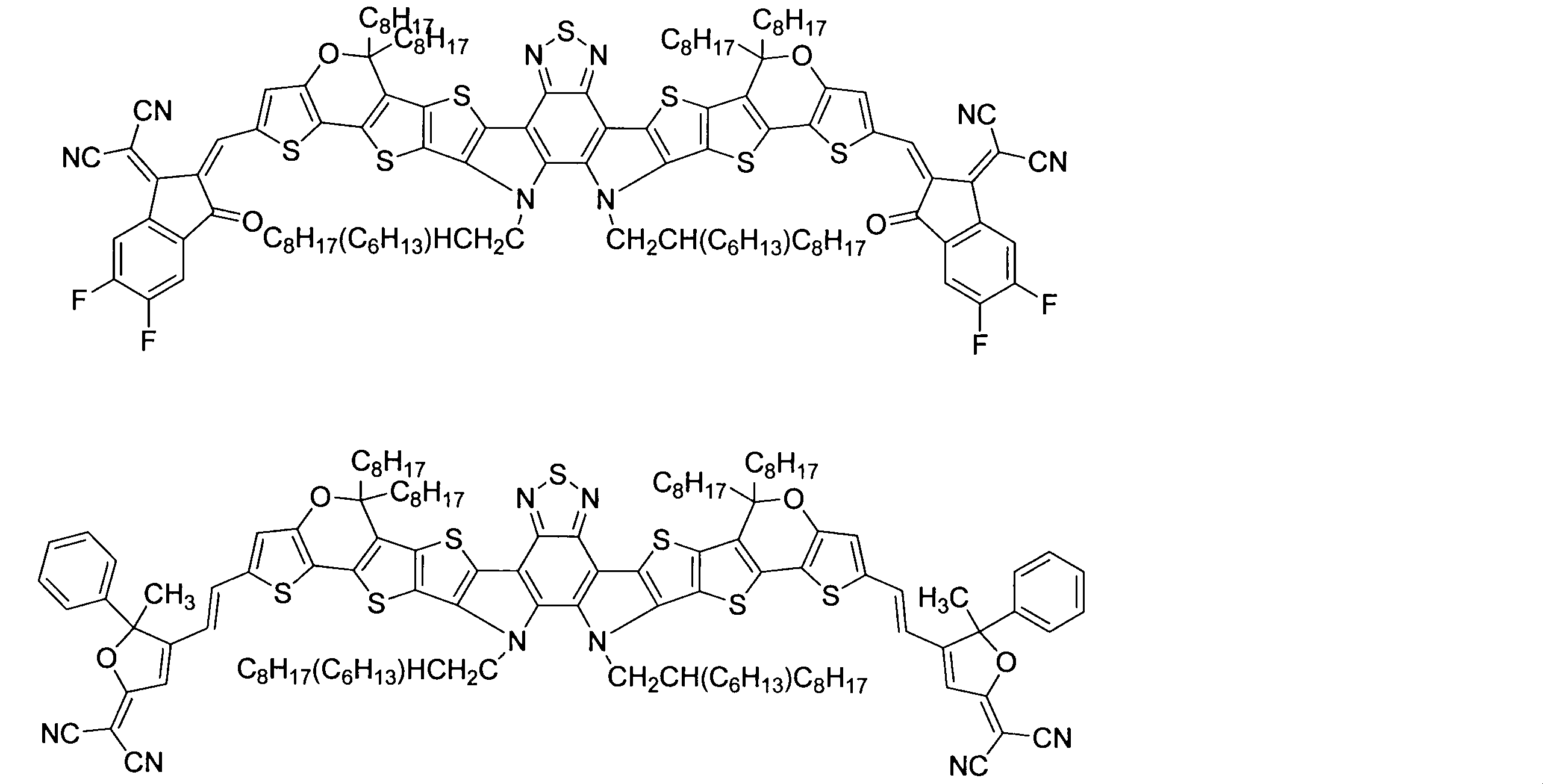
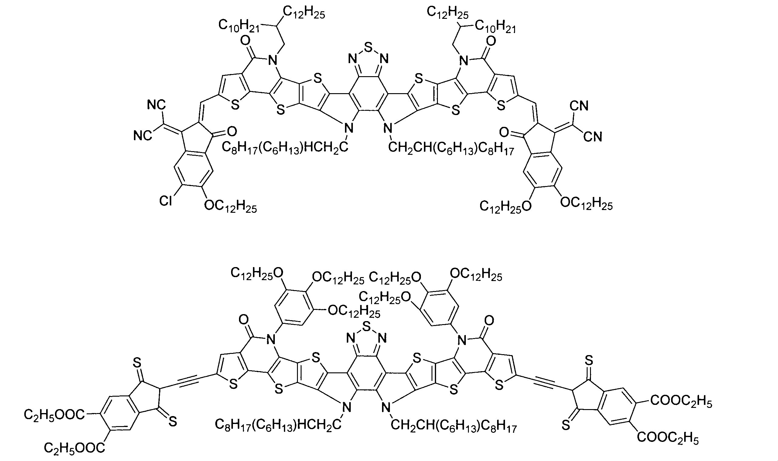
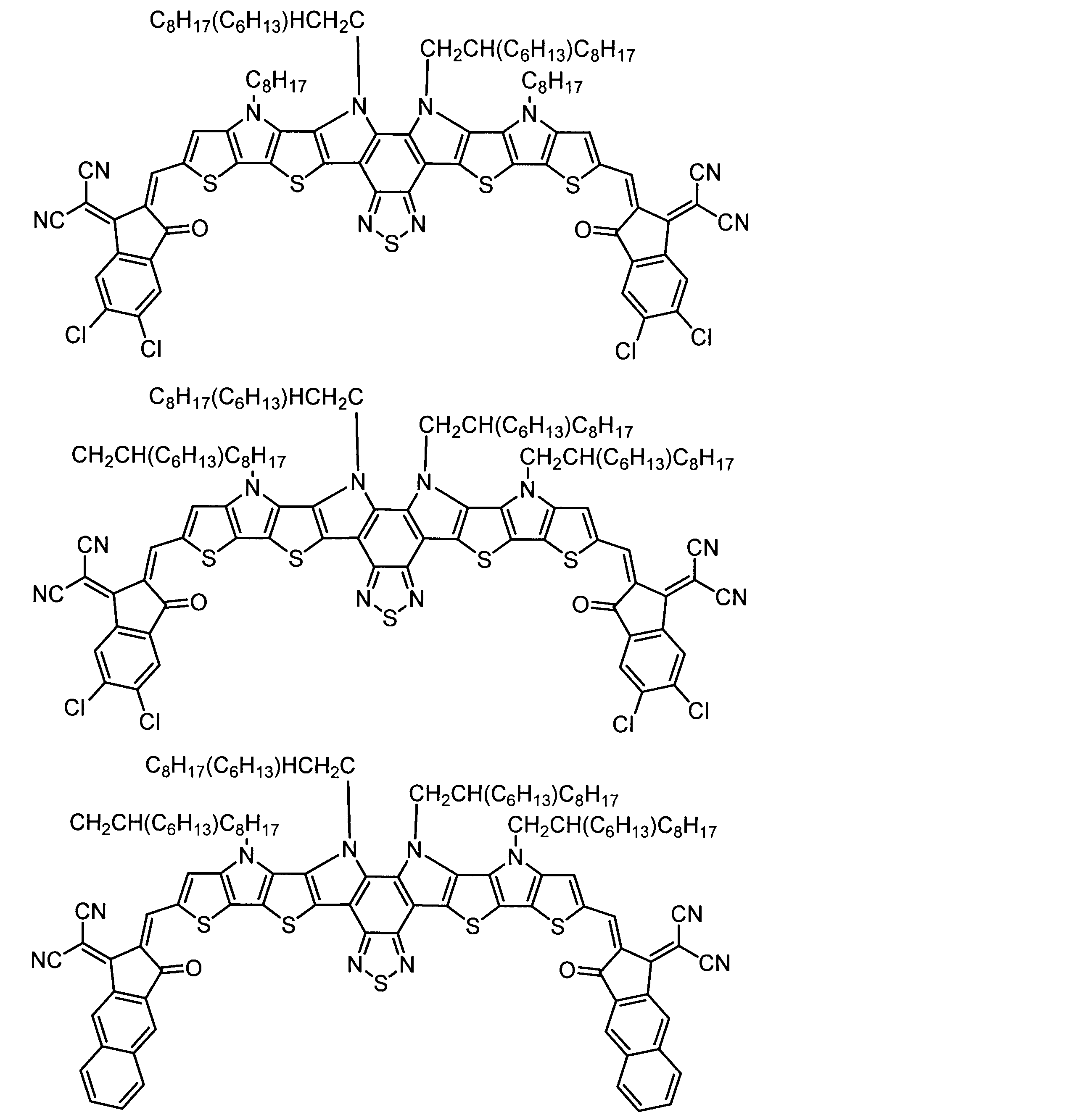


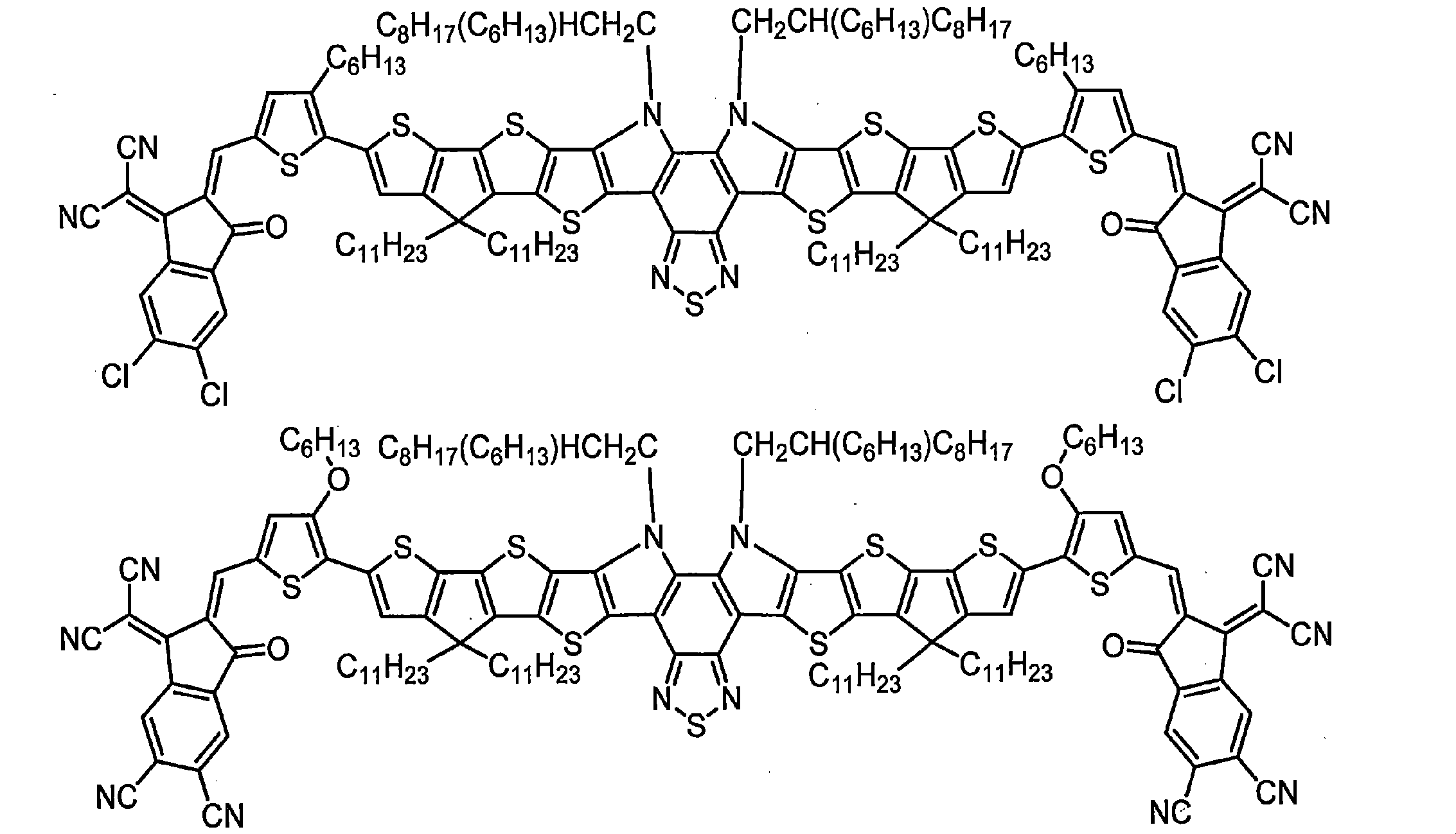
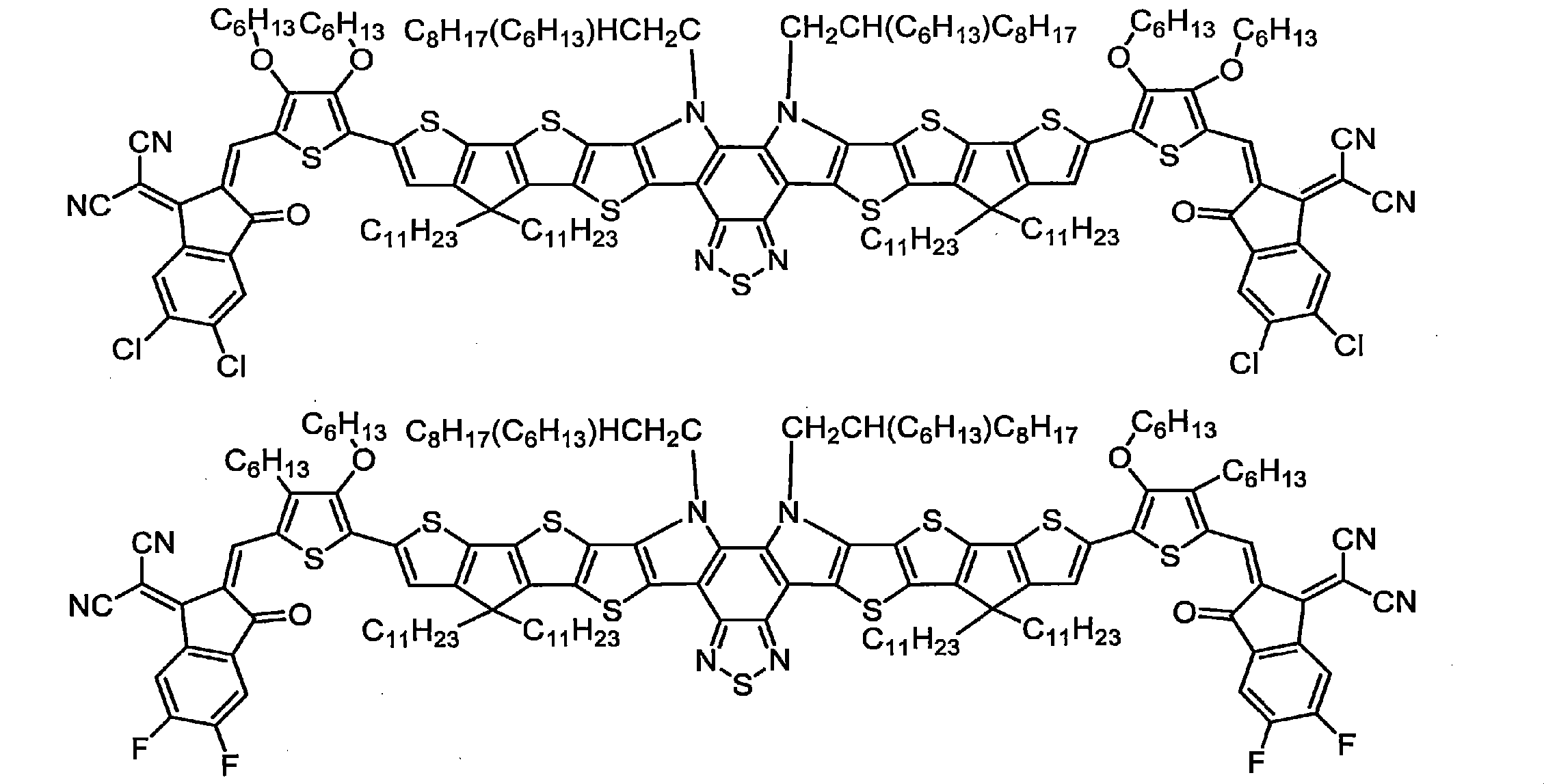
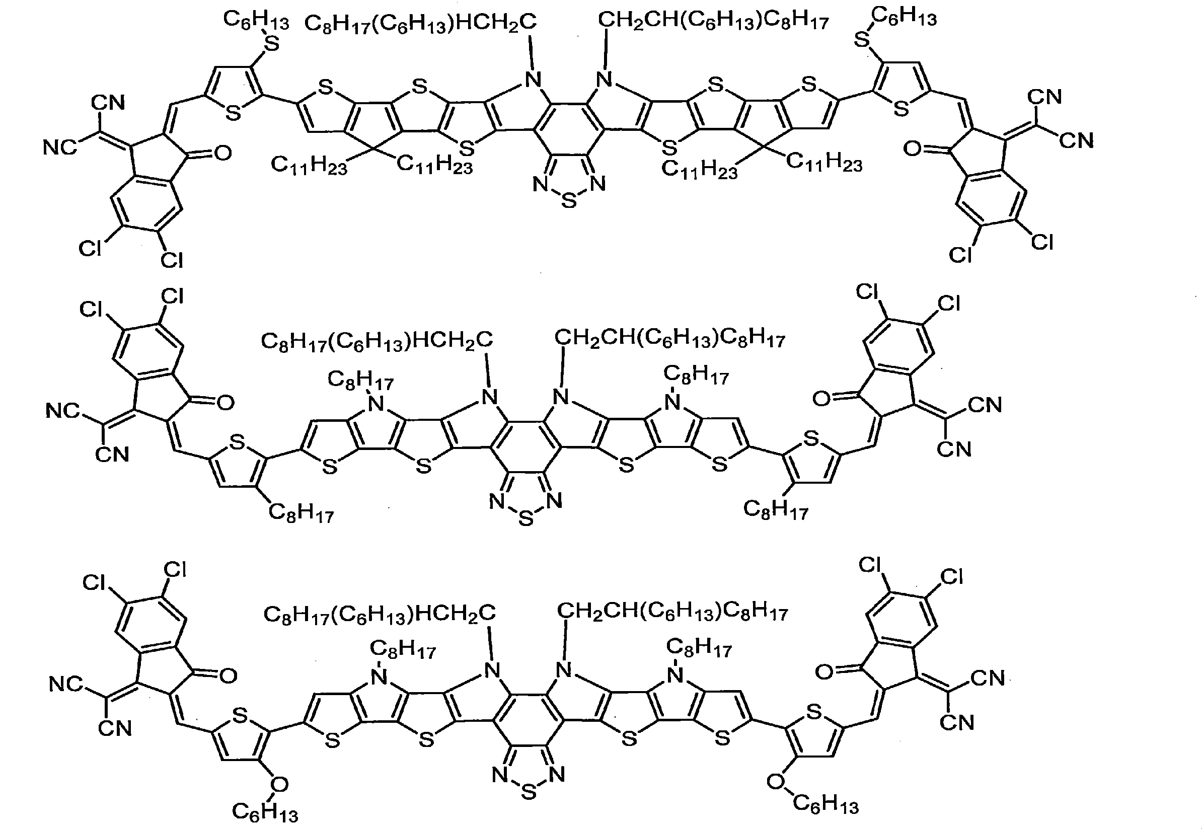

本実施形態の化合物は、光電変換素子(詳細については後述する。)の活性層の材料、特にn型半導体材料である非フラーレン化合物として好適に用いることができる。
本実施形態の化合物を、特にn型半導体材料として光電変換素子の活性層に用いれば、光電変換素子(光検出素子)における暗電流をより効果的に低減させることができる。
n型半導体材料として用いられる本実施形態の化合物は、2種以上が活性層の材料として含まれていてもよい。
2.化合物の製造方法
本実施形態の化合物の製造方法について説明する。
本実施形態の化合物の製造方法について説明する。
本実施形態の化合物は、例えば、既に説明したA1、A2、P、さらにはAr3及びAr4を構成することができる2以上の原料化合物を用いて、従来公知の任意好適な方法又は後述する実施例により示される方法により製造(合成)することができる。
本発明は、下記式(3)で表される化合物にも関する。すなわち、本発明は、既に説明した式(I)で表される化合物の製造に好適である原料化合物にも関する。

式(3)中、
Xは、-S-で表される基、-O-で表される基、-Se-で表される基、又は-N(R)-で表される基を表し、
Y1及びY2は、それぞれ独立して、-S-で表される基、-CR1R2-で表される基、-SiR1R2-で表される基、-NR-で表される基、-C(=O)-で表される基、-C(=O)-NR-で表される基、-CR1R2-O-で表される基、-O-CR1R2-で表される基、-C(=O)-CR1R2-で表される基、又は-CR1R2-C(=O)-で表される基を表し、
Ar1及びAr2は、それぞれ独立して、置換基を有していてもよく複数の環構造がさらに縮環していてもよい芳香族炭素環又は置換基を有していてもよく複数の環構造がさらに縮環していてもよい芳香族複素環を表し、
R、R1及びR2は、それぞれ独立して、
水素原子、
ハロゲン原子、
置換基を有していてもよいアルキル基、
置換基を有していてもよいシクロアルキル基、
置換基を有していてもよいアリール基、
置換基を有していてもよいアルキルオキシ基、
置換基を有していてもよいシクロアルキルオキシ基、
置換基を有していてもよいアリールオキシ基、
置換基を有していてもよいアルキルチオ基、
置換基を有していてもよいシクロアルキルチオ基、
置換基を有していてもよいアリールチオ基、
置換基を有していてもよい1価の複素環基、
置換基を有していてもよい置換アミノ基、
置換基を有していてもよいアシル基、
置換基を有していてもよいイミン残基、
置換基を有していてもよいアミド基、
置換基を有していてもよい酸イミド基、
置換基を有していてもよい置換オキシカルボニル基、
置換基を有していてもよいアルケニル基、
置換基を有していてもよいシクロアルケニル基、
置換基を有していてもよいアルキニル基、
置換基を有していてもよいシクロアルキニル基、
シアノ基、
ニトロ基、
-C(=O)-Raで表される基、又は
-SO2-Rbで表される基を表し、
Ra及びRbは、それぞれ独立して、
水素原子、
置換基を有していてもよいアルキル基、
置換基を有していてもよいアリール基、
置換基を有していてもよいアルキルオキシ基、
置換基を有していてもよいアリールオキシ基、又は
置換基を有していてもよい1価の複素環基を表し、
複数あるR、R1及びR2は、同一であっても異なっていてもよい。
式(3)中、X、Y1、Y2、Ar1、Ar2、R、R1及びR2の好ましい例等は、前記式(1)において既に説明したとおりである。式(3)中、Y1及びY2は-NR-で表される基であることが好ましい。
前記式(3)で表される化合物は、下記式(4)で表される化合物であることが好ましい。

前記式(4)中、
Y3及びY4は、それぞれ独立して、-S-で表される基、-CR1R2-で表される基、-SiR1R2-で表される基、-NR-で表される基、-C(=O)-で表される基、-C(=O)-NR-で表される基、-CR1R2-O-で表される基、-O-CR1R2-で表される基、-C(=O)-CR1R2-で表される基、又は-CR1R2-C(=O)-を表し、
X、R、R1及びR2は、前記定義のとおりである。
Wは、水素原子、ハロゲン原子、ホウ酸エステル残基、ジヒドロキシボリル基、ホルミル基、ビニル基又は置換スタンニル基を表す。2個あるWは、同一であっても異なっていてもよい。
Y3及びY4は、それぞれ独立して、-S-で表される基、-CR1R2-で表される基、-SiR1R2-で表される基、-NR-で表される基、-C(=O)-で表される基、-C(=O)-NR-で表される基、-CR1R2-O-で表される基、-O-CR1R2-で表される基、-C(=O)-CR1R2-で表される基、又は-CR1R2-C(=O)-を表し、
X、R、R1及びR2は、前記定義のとおりである。
Wは、水素原子、ハロゲン原子、ホウ酸エステル残基、ジヒドロキシボリル基、ホルミル基、ビニル基又は置換スタンニル基を表す。2個あるWは、同一であっても異なっていてもよい。
置換スタンニル基としては、-SnR100
3で表される基等が挙げられる。ここでR100は1価の有機基を表す。1価の有機基としては、例えば、アルキル基及びアリール基が挙げられる。
R100であるアルキル基としてはメチル基、エチル基、プロピル基、イソプロピル基、ブチル基、イソブチル基、sec-ブチル基、tert-ブチル基、ペンチル基、イソペンチル基、2-メチルブチル基、1-メチルブチル基、ヘキシル基、イソヘキシル基、3-メチルペンチル基、2一メチルペンチル基、1-メチルペンチル基、ヘプチル基、オクチル基、イソオクチル基、2-エチルヘキシル基、ノニル基、デシル基、ウンデシル基、ドデシル基、テトラデシル基、ヘキサデシル基、オクタデシル基、エイコシル基等の鎖状アルキル基、シクロペンチル基、シクロヘキシル基、アダマンチル基等のシクロアルキル基が挙げられる。アリール基としてはフェニル基、ナフチル基が挙げられる。置換スタンニル基として好ましくは、-SnMe3、-SnEt3、-SnBu3及び-SnPh3であり、より好ましくは、-SnMe3、-SnEt3及び-SnBu3である。上記式中、Meはメチル基を表し、Etはエチル基を表し、Buはブチル基を表し、Phはフェニル基を表す。
ホウ酸エステル残基は、ホウ酸ジエステルから水酸基を除いた基を表す。ホウ酸エステル残基の具体例としては、下記式で表される基が挙げられる。

前記式中、Meはメチル基を表し、Etはエチル基を表す。
前記式(3)及び式(4)で表される化合物の好適な具体例としては下記式で表される化合物が挙げられる。

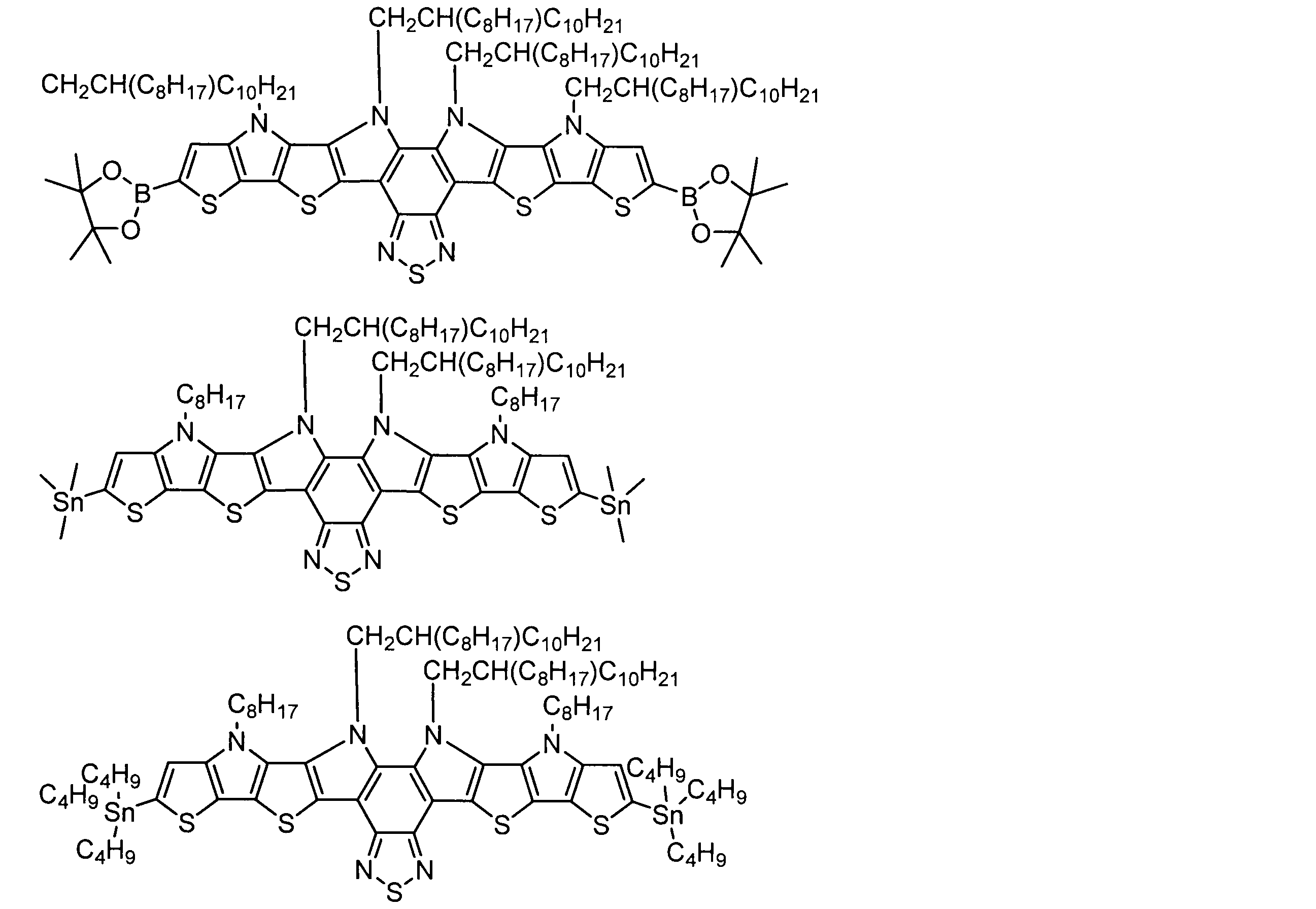

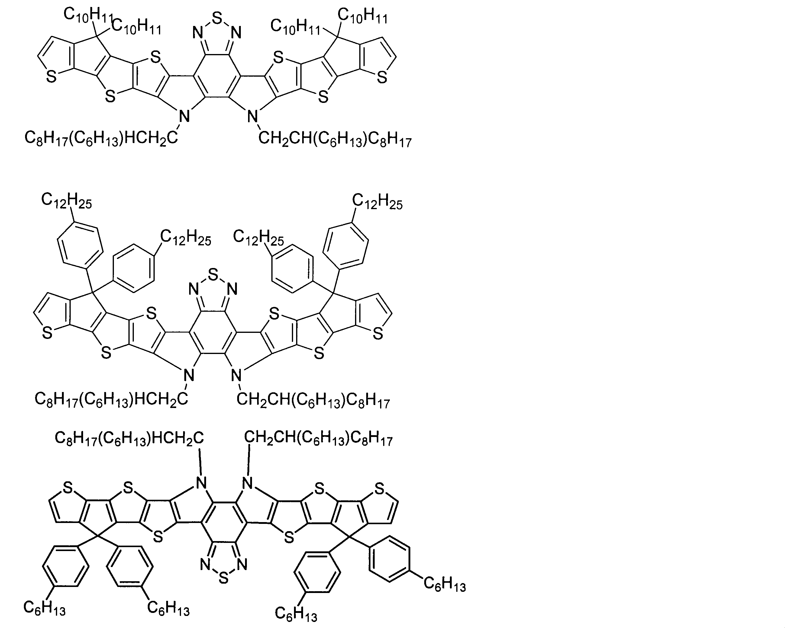
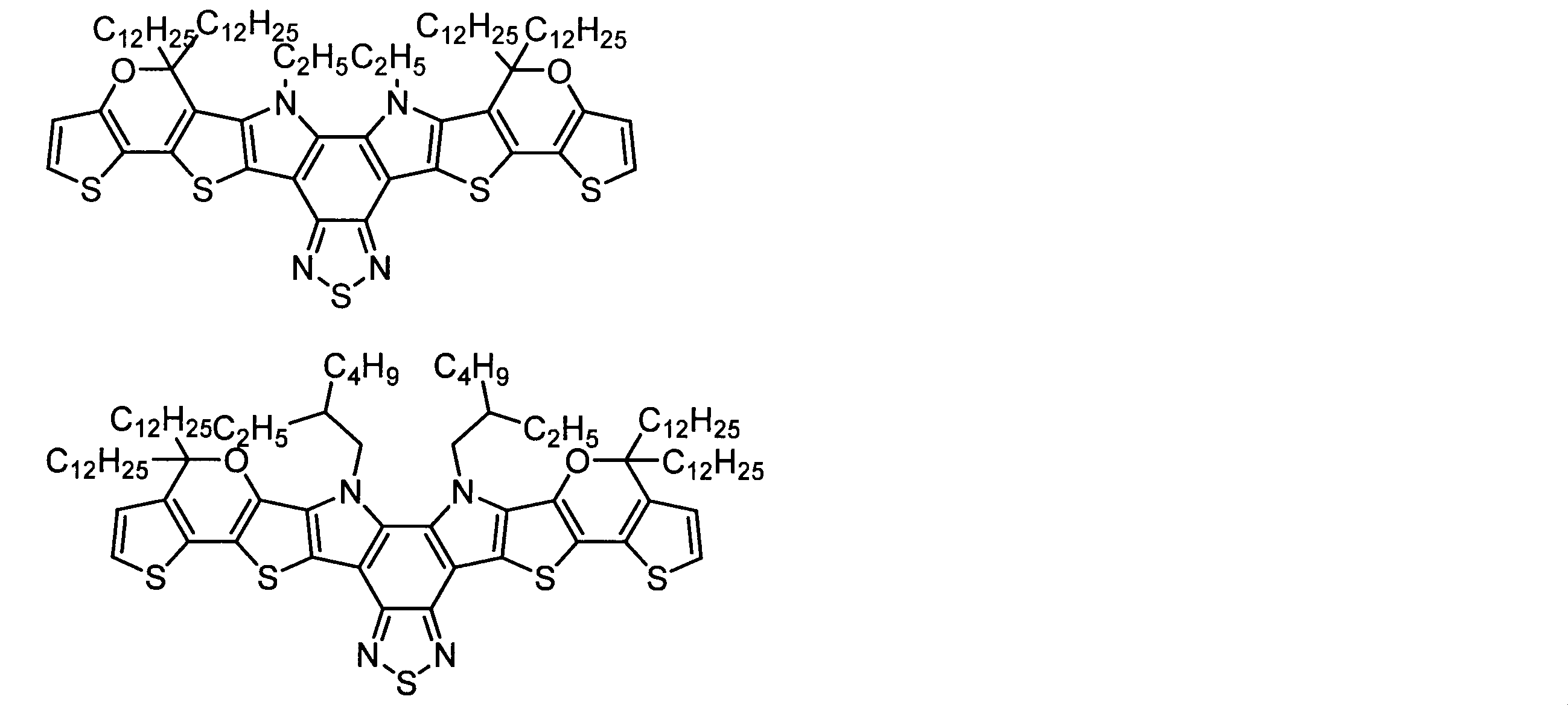
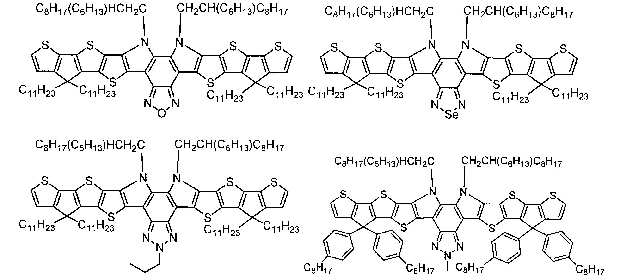
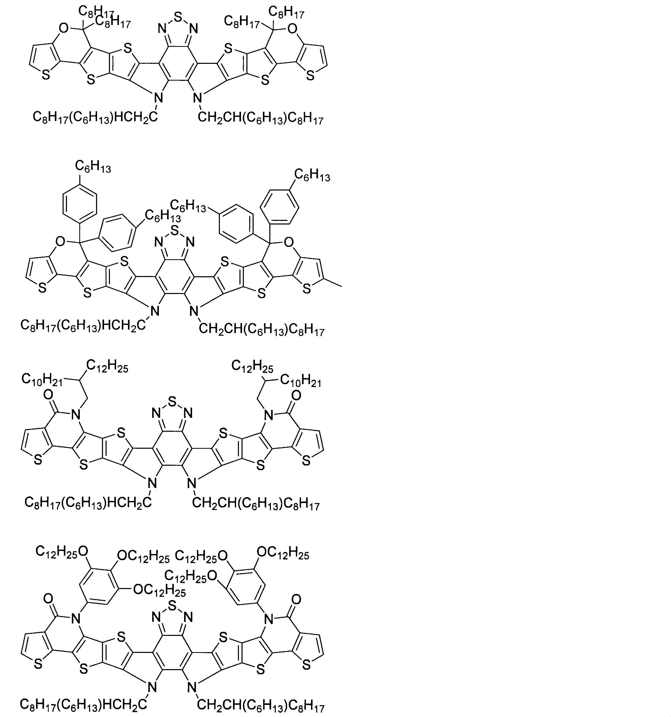
本実施形態において、光電変換素子の活性層は、特にn型半導体材料として本実施形態の化合物のみを含んでいてもよく、実施形態の化合物以外の化合物を、さらなるn型半導体材料として含んでいてもよい。さらなるn型半導体材料として含まれうる本実施形態の化合物以外の化合物は、低分子化合物であっても高分子化合物であってもよい。
低分子化合物である「本実施形態の化合物」以外のn型半導体材料(電子受容性化合物)の例としては、オキサジアゾール誘導体、アントラキノジメタン及びその誘導体、ベンゾキノン及びその誘導体、ナフトキノン及びその誘導体、アントラキノン及びその誘導体、テトラシアノアントラキノジメタン及びその誘導体、フルオレノン誘導体、ジフェニルジシアノエチレン及びその誘導体、ジフェノキノン誘導体、8-ヒドロキシキノリン及びその誘導体の金属錯体、並びに、バソクプロイン等のフェナントレン誘導体が挙げられる。
高分子化合物である「本実施形態の化合物」以外のn型半導体材料の例としては、ポリビニルカルバゾール及びその誘導体、ポリシラン及びその誘導体、側鎖又は主鎖に芳香族アミン構造を有するポリシロキサン誘導体、ポリアニリン及びその誘導体、ポリチオフェン及びその誘導体、ポリピロール及びその誘導体、ポリフェニレンビニレン及びその誘導体、ポリチエニレンビニレン及びその誘導体、ポリキノリン及びその誘導体、ポリキノキサリン及びその誘導体、並びに、ポリフルオレン及びその誘導体が挙げられる。
「本実施形態の化合物」以外の化合物には、フラーレン誘導体が含まれうる。
ここで、フラーレン誘導体とは、フラーレン(C60フラーレン、C70フラーレン、C76フラーレン、C78フラーレン、及びC84フラーレン)のうちの少なくとも一部が修飾された化合物をいう。換言すると、フラーレン骨格に付加された1つ以上の基を有する化合物をいう。以下、特にC60フラーレンのフラーレン誘導体を「C60フラーレン誘導体」といい、C70フラーレンのフラーレン誘導体を「C70フラーレン誘導体」という場合がある。
「本実施形態の化合物」以外のn型半導体材料として用いられうるフラーレン誘導体は、本発明の目的を損なわない限り特に限定されない。
「本実施形態の化合物」以外のn型半導体材料として用いられうるC60フラーレン誘導体の具体例としては、下記の化合物が挙げられる。
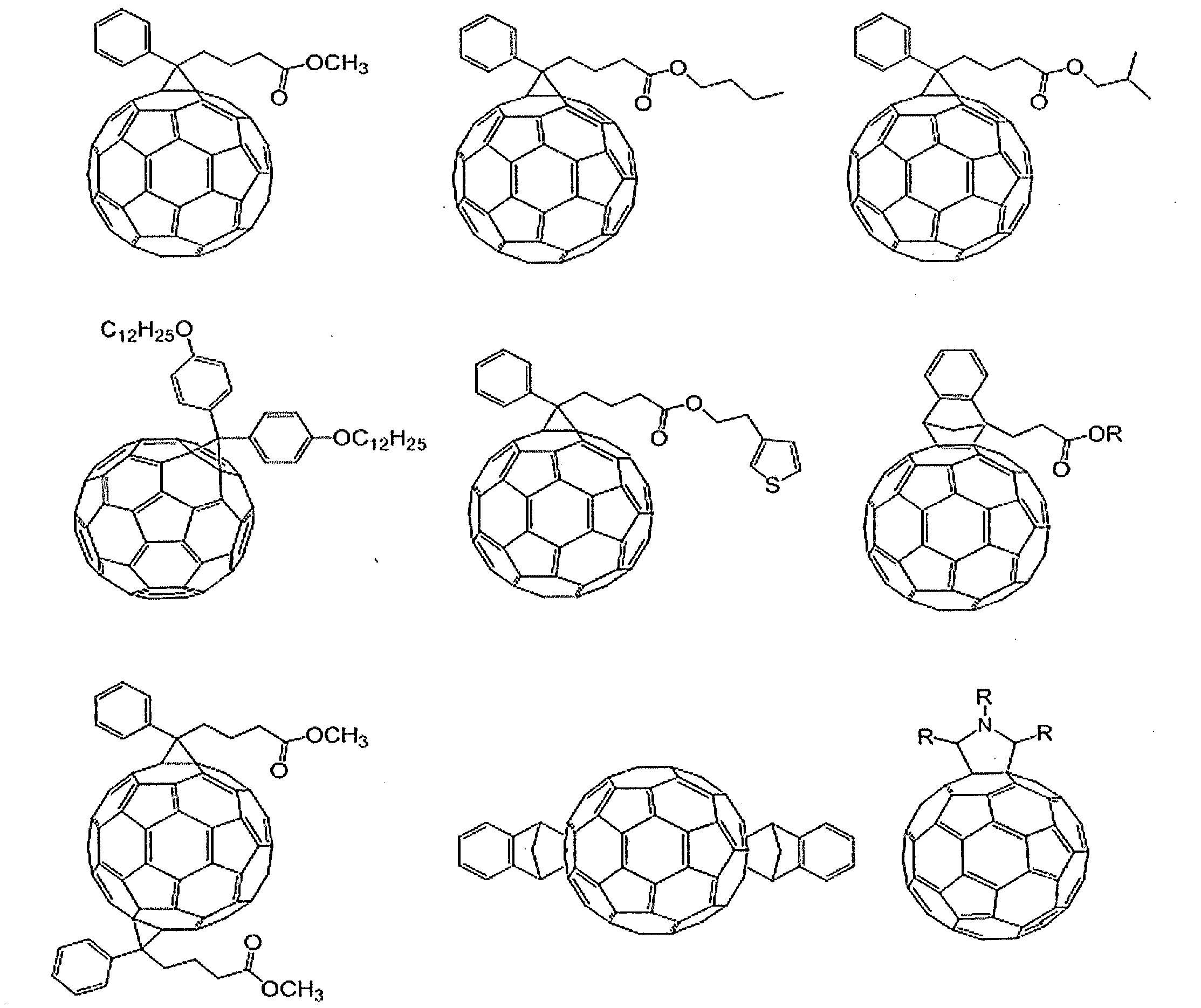
式中、Rは前記定義のとおりである。Rが複数ある場合、複数あるRは、互いに同一であっても異なっていてもよい。
C70フラーレン誘導体の例としては、下記の化合物が挙げられる。
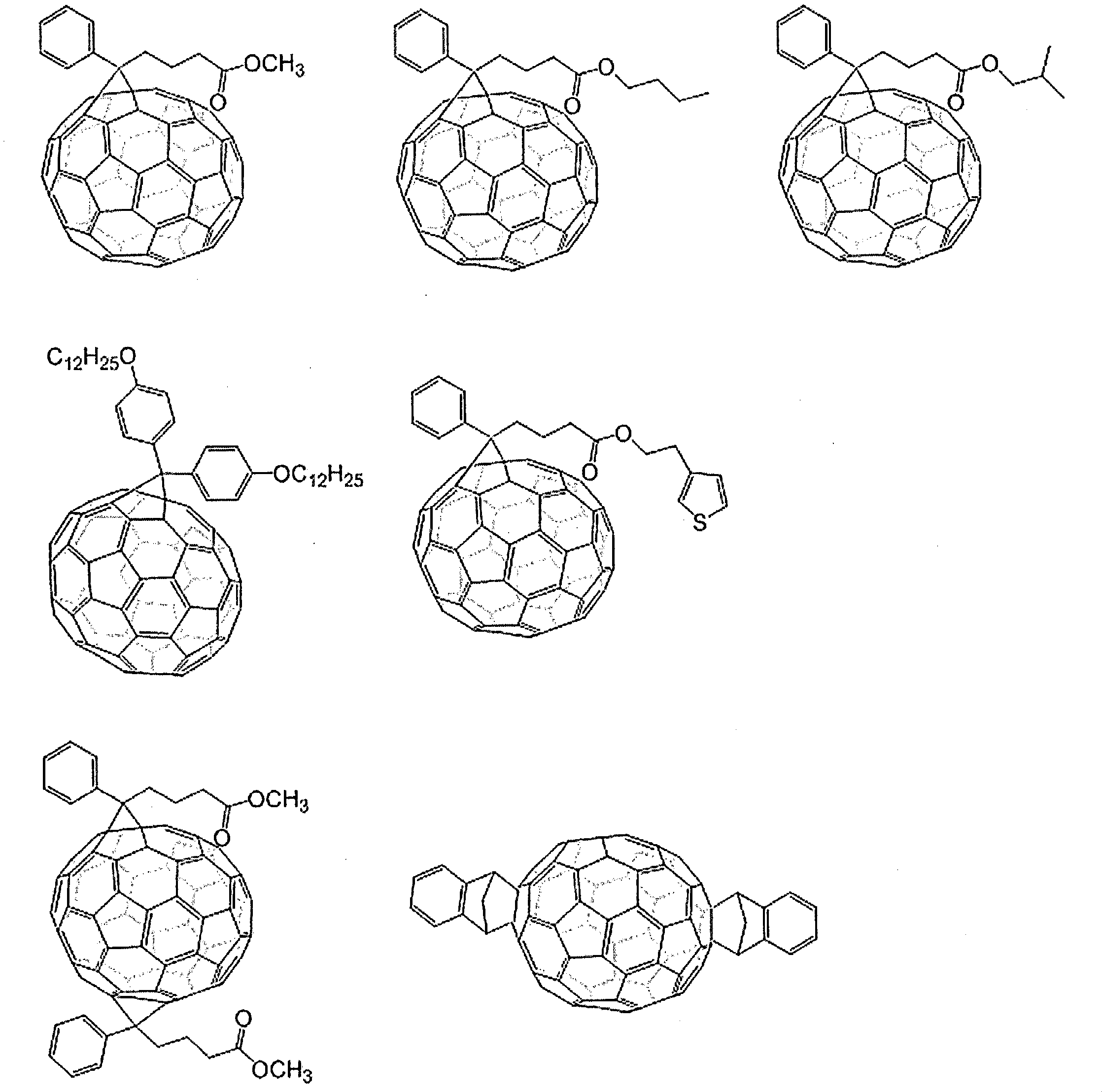
3.光電変換素子
本実施形態にかかる光電変換素子は、陽極と、陰極と、該陽極と該陰極との間に設けられており、p型半導体材料及びn型半導体材料を含む活性層とを含み、該n型半導体材料として、既に説明した本実施形態の化合物を含む、光電変換素子である。
本実施形態にかかる光電変換素子は、陽極と、陰極と、該陽極と該陰極との間に設けられており、p型半導体材料及びn型半導体材料を含む活性層とを含み、該n型半導体材料として、既に説明した本実施形態の化合物を含む、光電変換素子である。
本実施形態の光電変換素子によれば、上記の構成を有することにより、光電変換素子の製造工程又は光電変換素子が適用されるデバイスへの組み込み工程などにおける加熱処理に対する外部量子効率の低下を抑制し、耐熱性を効果的に向上させることができる。
ここで、本実施形態の光電変換素子が取りうる構成例について説明する。図1は、本実施形態の光電変換素子の構成を模式的に示す図である。
図1に示されるように、光電変換素子10は、支持基板11に設けられている。光電変換素子10は、支持基板11に接するように設けられている陽極12と、陽極12に接するように設けられている正孔輸送層13と、正孔輸送層13に接するように設けられている活性層14と、活性層14に接するように設けられている電子輸送層15と、電子輸送層15に接するように設けられている陰極16とを備えている。この構成例では、陰極16に接するように封止部材17がさらに設けられている。
以下、本実施形態の光電変換素子に含まれうる構成要素について具体的に説明する。
(基板)
光電変換素子は、通常、基板(支持基板)上に形成される。また、さらに基板(封止基板)により封止される場合もある。基板には、通常、陽極及び陰極からなる一対の電極のうちの一方が形成される。基板の材料は、特に有機化合物を含む層を形成する際に化学的に変化しない材料であれば特に限定されない。
光電変換素子は、通常、基板(支持基板)上に形成される。また、さらに基板(封止基板)により封止される場合もある。基板には、通常、陽極及び陰極からなる一対の電極のうちの一方が形成される。基板の材料は、特に有機化合物を含む層を形成する際に化学的に変化しない材料であれば特に限定されない。
基板の材料としては、例えば、ガラス、プラスチック、高分子フィルム、シリコンが挙げられる。不透明な基板が用いられる場合には、不透明な基板側に設けられる電極とは反対側の電極(換言すると、不透明な基板から遠い側の電極)が透明又は半透明の電極とされることが好ましい。
(電極)
光電変換素子は、一対の電極である陽極及び陰極を含んでいる。陽極及び陰極のうち、少なくとも一方の電極は、光を入射させるために、透明又は半透明の電極とすることが好ましい。
光電変換素子は、一対の電極である陽極及び陰極を含んでいる。陽極及び陰極のうち、少なくとも一方の電極は、光を入射させるために、透明又は半透明の電極とすることが好ましい。
透明又は半透明の電極の材料の例としては、導電性の金属酸化物膜、半透明の金属薄膜が挙げられる。具体的には、酸化インジウム、酸化亜鉛、酸化スズ、及びそれらの複合体であるインジウムスズ酸化物(ITO)、インジウム亜鉛酸化物(IZO)、NESA等の導電性材料、金、白金、銀、銅が挙げられる。透明又は半透明である電極の材料としては、ITO、IZO、酸化スズが好ましい。また、電極として、ポリアニリン及びその誘導体、ポリチオフェン及びその誘導体などの有機化合物が材料として用いられる透明導電膜を用いてもよい。透明又は半透明の電極は、陽極であっても陰極であってもよい。
一対の電極のうちの一方の電極が透明又は半透明であれば、他方の電極は光透過性の低い電極であってもよい。光透過性の低い電極の材料の例としては、金属、及び導電性高分子が挙げられる。光透過性の低い電極の材料の具体例としては、リチウム、ナトリウム、カリウム、ルビジウム、セシウム、マグネシウム、カルシウム、ストロンチウム、バリウム、アルミニウム、スカンジウム、バナジウム、亜鉛、イットリウム、インジウム、セリウム、サマリウム、ユーロピウム、テルビウム、イッテルビウム等の金属、及びこれらのうちの2種以上の合金、又は、これらのうちの1種以上の金属と、金、銀、白金、銅、マンガン、チタン、コバルト、ニッケル、タングステン及び錫からなる群から選ばれる1種以上の金属との合金、グラファイト、グラファイト層間化合物、ポリアニリン及びその誘導体、ポリチオフェン及びその誘導体が挙げられる。合金としては、マグネシウム-銀合金、マグネシウム-インジウム合金、マグネシウム-アルミニウム合金、インジウム-銀合金、リチウム-アルミニウム合金、リチウム-マグネシウム合金、リチウム-インジウム合金、及びカルシウム-アルミニウム合金が挙げられる。
(活性層)
本実施形態の光電変換素子が備える活性層は、バルクヘテロジャンクション型の構造を有することが想定されており、p型半導体材料と、n型半導体材料とを含み、該活性層が、n型半導体材料として、本実施形態の化合物を含む(詳細については後述する。)。
本実施形態の光電変換素子が備える活性層は、バルクヘテロジャンクション型の構造を有することが想定されており、p型半導体材料と、n型半導体材料とを含み、該活性層が、n型半導体材料として、本実施形態の化合物を含む(詳細については後述する。)。
本実施形態において、活性層の厚さは、特に限定されない。活性層の厚さは、暗電流の抑制と生じた光電流の取り出しとのバランスを考慮して、任意好適な厚さとすることができる。活性層の厚さは、特に暗電流をより低減する観点から、好ましくは100nm以上であり、より好ましくは150nm以上であり、さらに好ましくは200nm以上である。また、活性層の厚さは、好ましくは10μm以下であり、より好ましくは5μm以下であり、さらに好ましくは1μm以下である。
本実施形態において活性層は、200℃以上の加熱温度で加熱される処理を含む工程により形成される(詳細は後述する。)。
ここで、本実施形態にかかる活性層の材料として、既に説明した本実施形態の化合物であるn型半導体材料と組み合わせて好適に用いることができるp型半導体材料について説明する。
p型半導体材料は、所定のポリスチレン換算の重量平均分子量を有する高分子化合物であることが好ましい。
ここで、ポリスチレン換算の重量平均分子量とは、ゲルパーミエーションクロマトグラフィー(GPC)を用い、ポリスチレンの標準試料を用いて算出した重量平均分子量を意味する。
p型半導体材料のポリスチレン換算の重量平均分子量は、特に溶媒に対する溶解性を向上させる観点から、3000以上500000以下であることが好ましい。
本実施形態において、p型半導体材料は、ドナー構成単位(D構成単位ともいう。)とアクセプター構成単位(A構成単位ともいう。)とを含むπ共役高分子化合物(D-A型共役高分子化合物ともいう。)であることが好ましい。なお、いずれがドナー構成単位又はアクセプター構成単位であるかは、HOMO又はLUMOのエネルギーレベルから相対的に決定しうる。
ここで、ドナー構成単位はπ電子が過剰である構成単位であり、アクセプター構成単位はπ電子が欠乏している構成単位である。
本実施形態において、p型半導体材料を構成しうる構成単位には、ドナー構成単位とアクセプター構成単位とが直接的に結合した構成単位、さらにはドナー構成単位とアクセプター構成単位とが、任意好適なスペーサー(基又は構成単位)を介して結合した構成単位も含まれる。
高分子化合物であるp型半導体材料としては、例えば、ポリビニルカルバゾール及びその誘導体、ポリシラン及びその誘導体、側鎖又は主鎖に芳香族アミン構造を含むポリシロキサン誘導体、ポリアニリン及びその誘導体、ポリチオフェン及びその誘導体、ポリピロール及びその誘導体、ポリフェニレンビニレン及びその誘導体、ポリチエニレンビニレン及びその誘導体、ポリフルオレン及びその誘導体が挙げられる。
本実施形態のp型半導体材料は、下記式(II)で表される構成単位を含む高分子化合物であることが好ましい。下記式(II)で表される構成単位は、本実施形態においては、通常、ドナー構成単位である。

式(II)中、Ar5及びAr6は、置換基を有していてもよい3価の芳香族複素環基を表し、Zは下記式(Z-1)~式(Z-7)で表される基を表す。

式(Z-1)~(Z-7)中、
Rは、前記定義のとおりである。
式(Z-1)~式(Z-7)のそれぞれにおいて、Rが2つある場合、2つのRは互いに同一であっても異なっていてもよい。
Rは、前記定義のとおりである。
式(Z-1)~式(Z-7)のそれぞれにおいて、Rが2つある場合、2つのRは互いに同一であっても異なっていてもよい。
Ar5及びAr6を構成しうる芳香族複素環には、複素環自体が芳香族性を示す単環及び縮合環に加えて、環を構成する複素環自体は芳香族性を示さなくとも、複素環に芳香環が縮合している環が包含される。
Ar5及びAr6を構成しうる芳香族複素環は、それぞれ単環であってもよく、縮合環であってもよい。芳香族複素環が縮合環である場合、縮合環を構成する環の全部が芳香族性を有する縮合環であってもよく、一部のみが芳香族性を有する縮合環であってもよい。
これらの環が複数の置換基を有する場合、これらの置換基は、同一であっても異なっていてもよい。
これらの環が複数の置換基を有する場合、これらの置換基は、同一であっても異なっていてもよい。
Ar5及びAr6を構成しうる芳香族炭素環の具体例としては、ベンゼン環、ナフタレン環、アントラセン環、テトラセン環、ペンタセン環、ピレン環、及びフェナントレン環が挙げられ、好ましくはベンゼン環及びナフタレン環であり、より好ましくはベンゼン環及びナフタレン環であり、さらに好ましくはベンゼン環である。これらの環は、置換基を有していてもよい。
芳香族複素環の具体例としては、芳香族複素環式化合物として既に説明した化合物が有する環構造が挙げられ、オキサジアゾール環、チアジアゾール環、チアゾール環、オキサゾール環、チオフェン環、ピロール環、ホスホール環、フラン環、ピリジン環、ピラジン環、ピリミジン環、トリアジン環、ピリダジン環、キノリン環、イソキノリン環、カルバゾール環、及びジベンゾホスホール環、並びに、フェノキサジン環、フェノチアジン環、ジベンゾボロール環、ジベンゾシロール環、及びベンゾピラン環が挙げられる。これらの環は、置換基を有していてもよい。
式(II)で表される構成単位は、下記式(II-1)、(II-2)又は(II-3)で表される構成単位であることが好ましい。

式(II-1)、(II-2)及び(II-3)中、Ar5、Ar6及びRは、前記定義のとおりである。
式(II)で表される好適な構成単位の具体例としては、下記式で表される構成単位が挙げられる。

前記式中、Rは前記定義のとおりである。
Rが2つある場合、2つあるRは同一であっても異なっていてもよい。
Rが2つある場合、2つあるRは同一であっても異なっていてもよい。
式(II)で表されるより具体的な好ましい構成単位の例としては、下記式で表される構成単位が挙げられる。
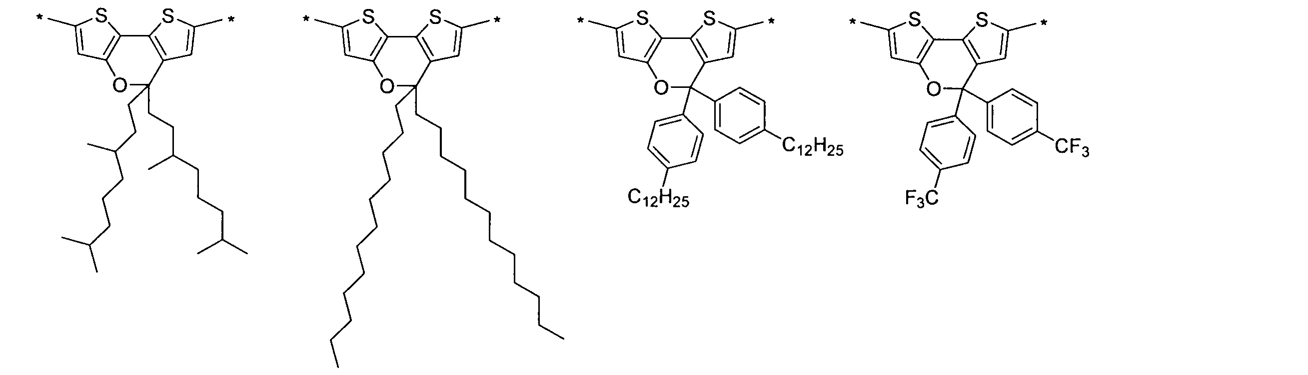
本実施形態においてp型半導体材料である高分子化合物は、下記式(III)で表される構成単位を含むことが好ましい。下記式(III)で表される構成単位は、本実施形態においては、通常、アクセプター構成単位である。

式(III)中、Ar7は2価の芳香族複素環基を表す。
Ar7で表される2価の芳香族複素環基の炭素原子数は、通常2~60であり、好ましくは4~60であり、より好ましくは4~20である。
Ar7で表される2価の芳香族複素環基は置換基を有していてもよい。Ar7で表される2価の芳香族複素環基が有していてもよい置換基の例としては、ハロゲン原子、置換基を有していてもよいアルキル基、置換基を有していてもよいアリール基、置換基を有していてもよいアルキルオキシ基、置換基を有していてもよいアリールオキシ基、置換基を有していてもよいアルキルチオ基、置換基を有していてもよいアリールチオ基、置換基を有していてもよい1価の複素環基、置換基を有していてもよい置換アミノ基、置換基を有していてもよいアシル基、置換基を有していてもよいイミン残基、置換基を有していてもよいアミド基、置換基を有していてもよい酸イミド基、置換基を有していてもよい置換オキシカルボニル基、置換基を有していてもよいアルケニル基、置換基を有していてもよいアルキニル基、シアノ基、及びニトロ基が挙げられる。
式(III)で表される構成単位としては、下記式(III-1)~式(III-10)で表される構成単位が好ましい。
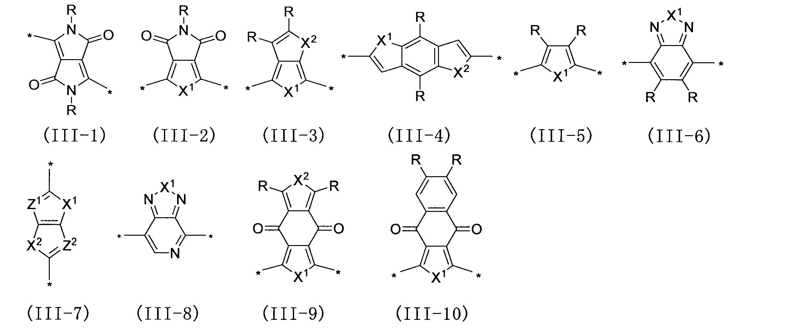
式(III-1)~式(III-10)中、
X1、X2、Z1、Z2及びRは前記定義のとおりである。
Rが2つある場合、2つあるRは、同一であっても異なっていてもよい。
X1、X2、Z1、Z2及びRは前記定義のとおりである。
Rが2つある場合、2つあるRは、同一であっても異なっていてもよい。
式(III-1)~式(III-10)中のX1及びX2は、原料化合物の入手性の観点から、いずれも硫黄原子であることが好ましい。
なお、式(III-1)~式(III-10)で表される構成単位は、上記のとおり、通常、アクセプター構成単位として機能しうる。しかしながらこれに限定されず、特に式(III-4)、式(III-5)及び式(III-7)で表される構成単位は、ドナー構成単位としても機能しうる。
本実施形態において、p型半導体材料は、チオフェン骨格を含む構成単位を含み、π共役系を含むπ共役高分子化合物であることが好ましい。
Ar7で表される2価の芳香族複素環基の具体例としては、下記式(101)~式(191)で表される基が挙げられる。これらの基はさらに置換基を有していてもよい。
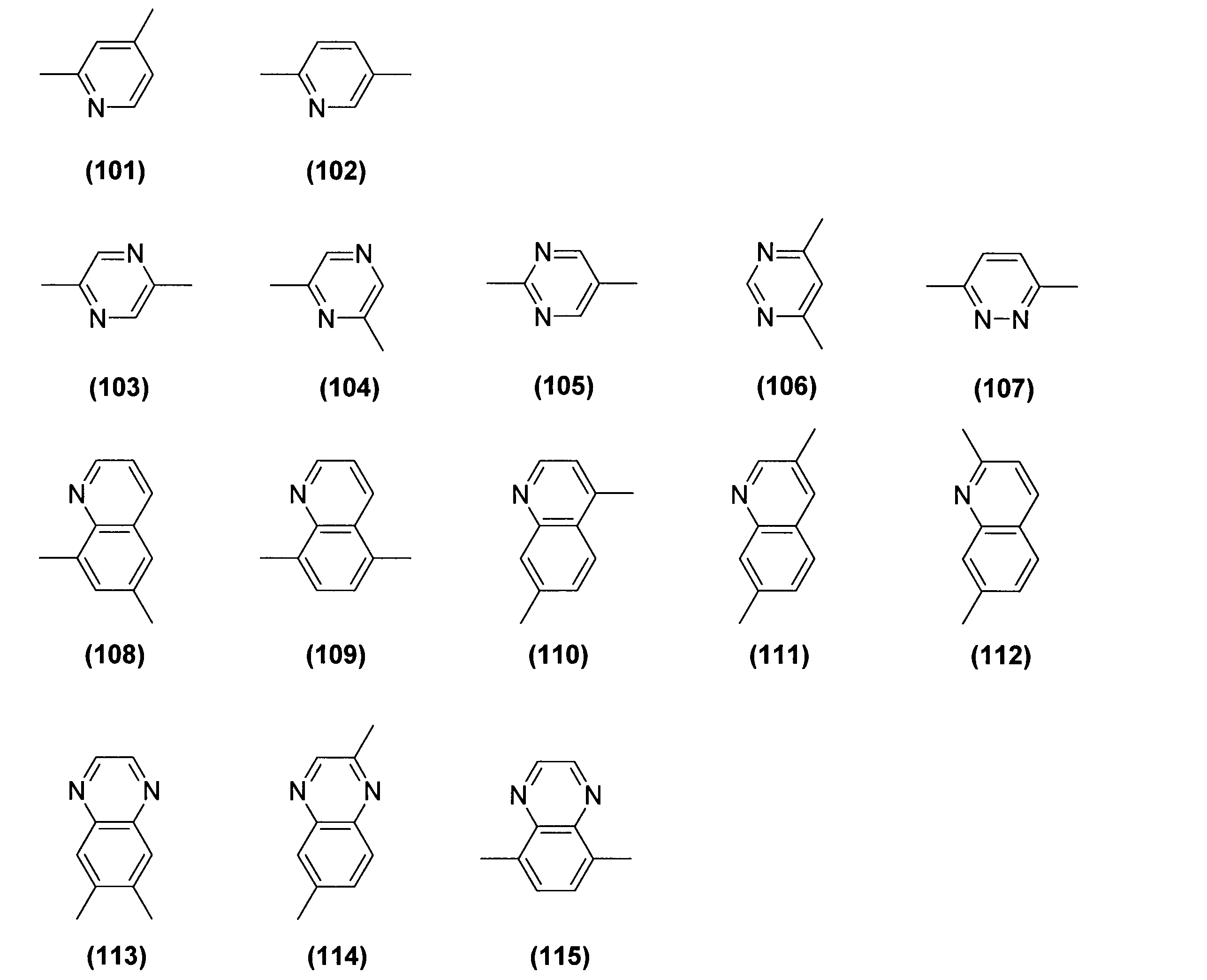
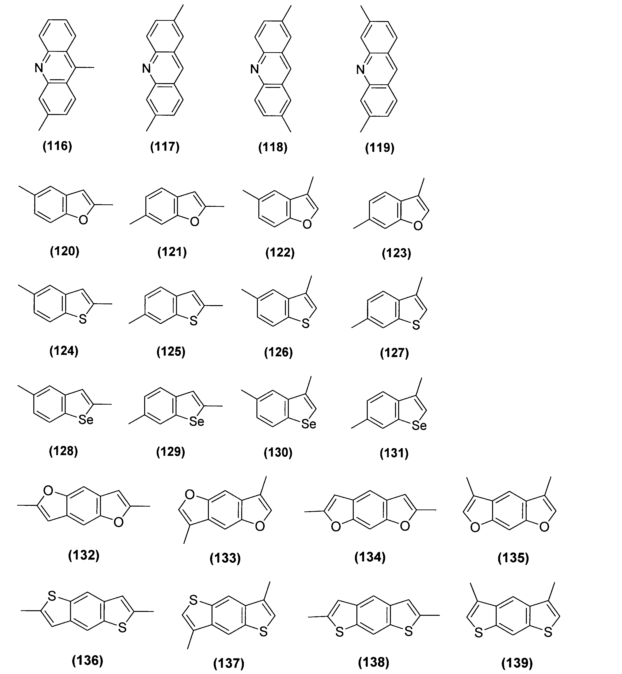
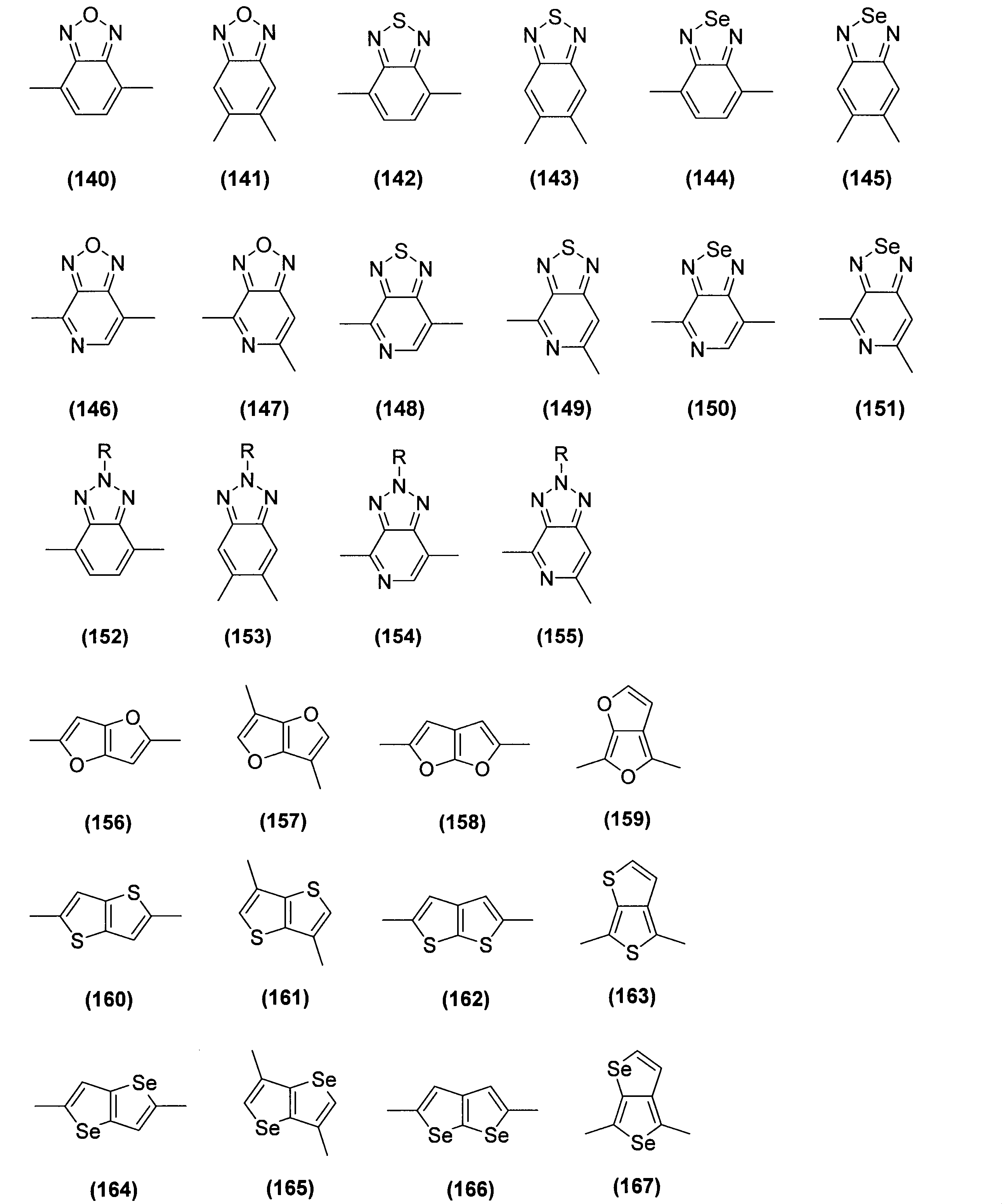

本実施形態のp型半導体材料である高分子化合物は、ドナー構成単位として式(II)で表される構成単位を含み、かつアクセプター構成単位として式(III)で表される構成単位を含むπ共役高分子化合物であることが好ましい。
本実施形態のp型半導体材料である高分子化合物において、p型半導体材料である高分子化合物は、既に説明した式(II)で表される構成単位と下記式(III)で現れる構成単位とが連結した構造を構成単位として含んでいてもよい。
本実施形態p型半導体材料である高分子化合物は、2種以上の式(II)で表される構成単位を含んでいてもよく、2種以上の式(III)で表される構成単位を含んでいてもよい。
例えば、溶媒に対する溶解性を向上させる観点から、本実施形態のp型半導体材料である高分子化合物は、下記式(IV)で表される構成単位を含んでいてもよい。

式(IV)中、Ar8はアリーレン基を表す。
Ar8で表されるアリーレン基とは、置換基を有していてもよい芳香族炭化水素から、水素原子を2個除いた残りの原子団を意味する。芳香族炭化水素には、縮合環を有する化合物、独立したベンゼン環及び縮合環からなる群から選ばれる2個以上が、直接的に又はビニレン基などの2価の基を介して結合した化合物も含まれる。
芳香族炭化水素が有していてもよい置換基の例としては、複素環式化合物が有していてもよい置換基として例示された置換基と同様の置換基が挙げられる。
Ar8で表されるアリーレン基の炭素原子数は、置換基の炭素原子数を含めないで通常6~60であり、好ましくは6~20である。置換基を含めたアリーレン基の炭素原子数は、通常6~100である。
Ar8で表されるアリーレン基の例としては、フェニレン基(例えば、下記式1~式3)、ナフタレン-ジイル基(例えば、下記式4~式13)、アントラセン-ジイル基(例えば、下記式14~式19)、ビフェニル-ジイル基(例えば、下記式20~式25)、ターフェニル-ジイル基(例えば、下記式26~式28)、縮合環化合物基(例えば、下記式29~式35)、フルオレン-ジイル基(例えば、下記式36~式38)、及びベンゾフルオレン-ジイル基(例えば、下記式39~式46)が挙げられる。

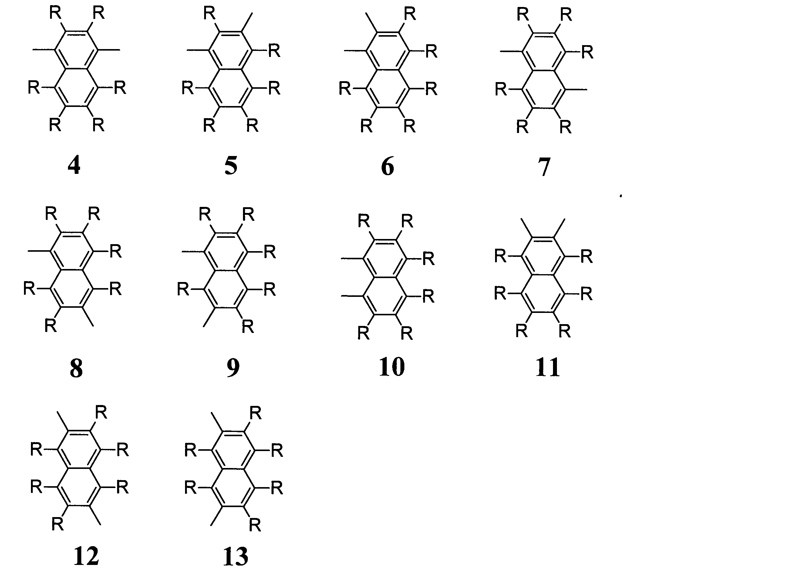
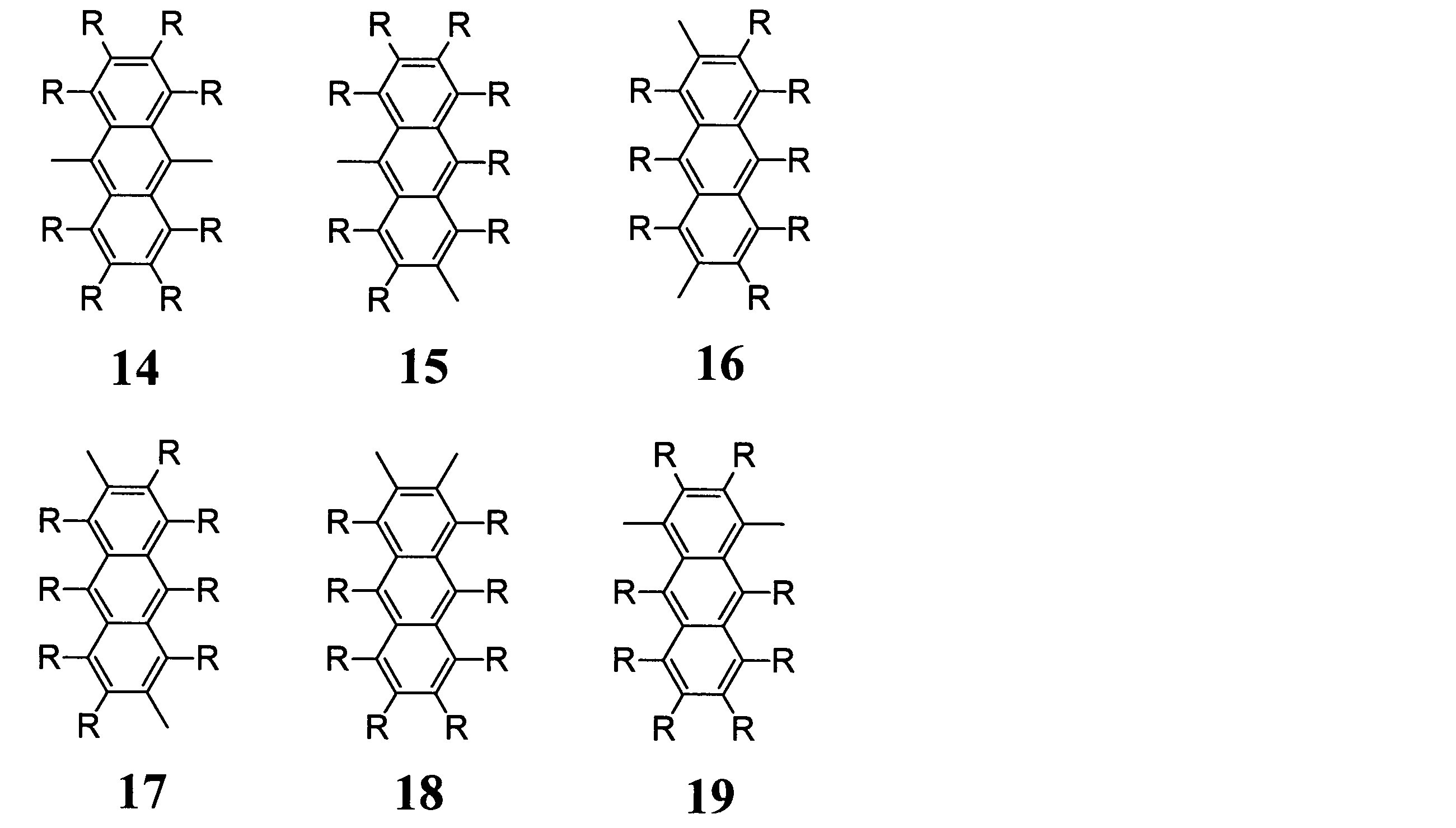
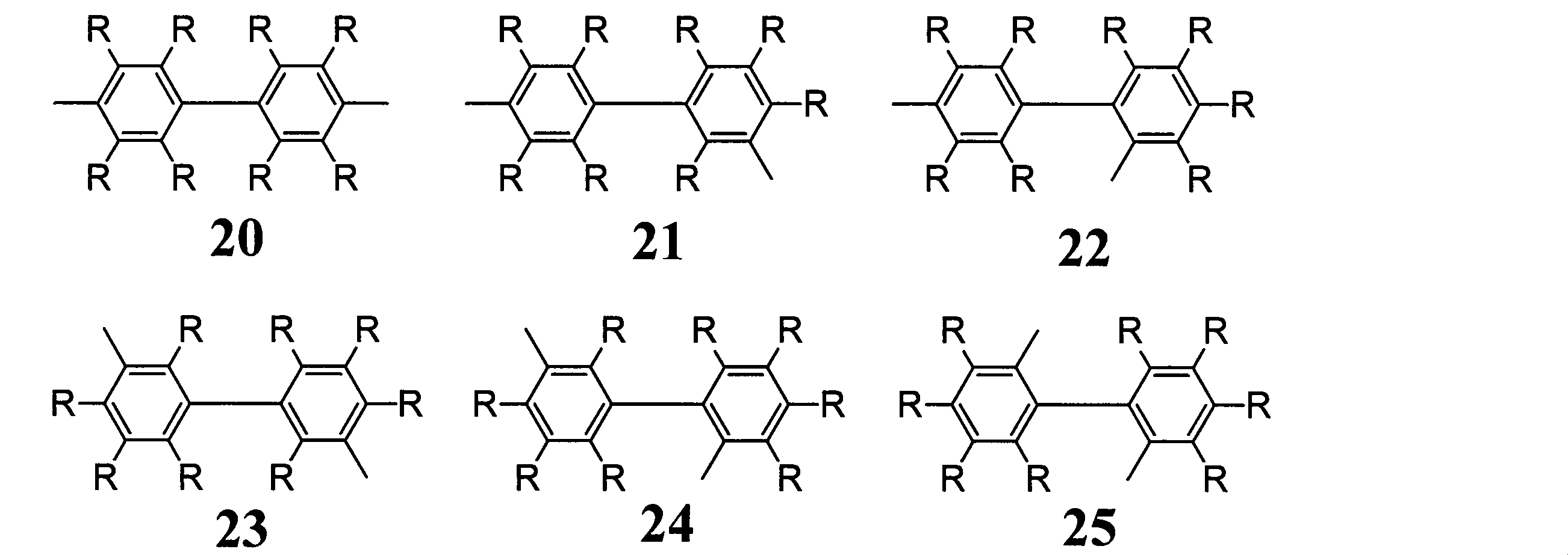
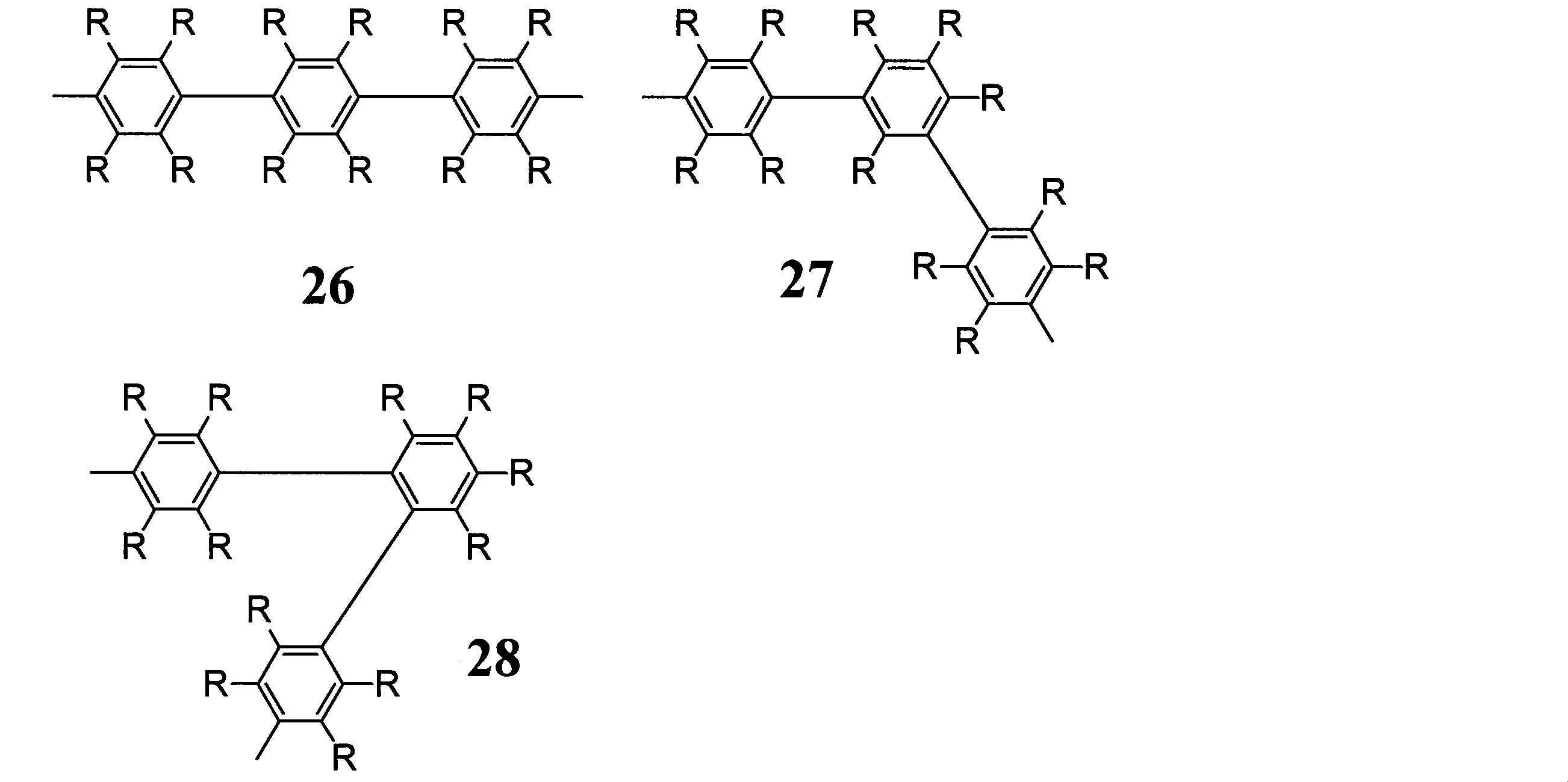

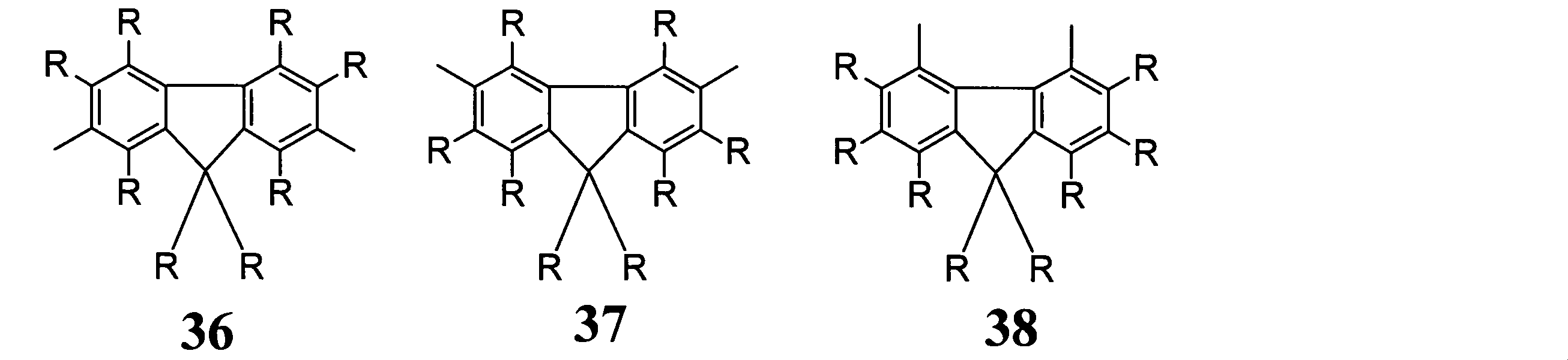
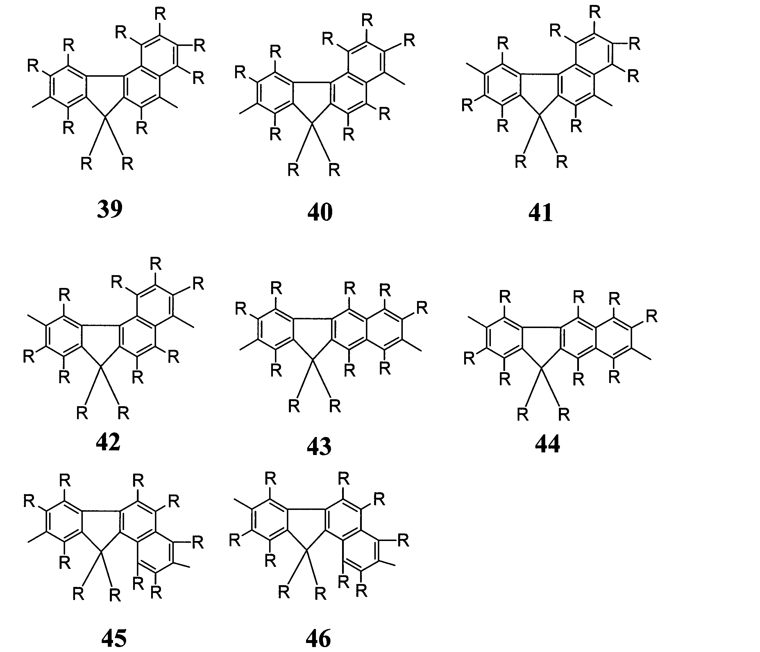
式中、Rは前記定義のとおりである。複数あるRは、同一であっても異なっていてもよい。
式(IV)で表される構成単位は、下記式(IV-1)及び式(IV-2)で表される構成単位であることが好ましい。

式(V)中、Rは、前記定義のとおりである。2つあるRは、同一であっても異なっていてもよい。
p型半導体材料である高分子化合物を構成する構成単位は、上記の構成単位から選択される2種以上の構成単位が2つ以上組み合わされて連結された構成単位であってもよい。
p型半導体材料としての高分子化合物が、式(II)で表される構成単位及び/又は式(III)で表される構成単位を含む場合、式(II)で表される構成単位及び式(III)で表される構成単位の合計量は、高分子化合物が含むすべての構成単位の量を100モル%とすると、通常20モル%~100モル%であり、p型半導体材料としての電荷輸送性を向上させる観点から、好ましくは40モル%~100モル%であり、より好ましくは50モル%~100モル%である。
本実施形態のp型半導体材料である高分子化合物の具体例としては、下記式(P-1)~(P-18)で表される高分子化合物が挙げられる。

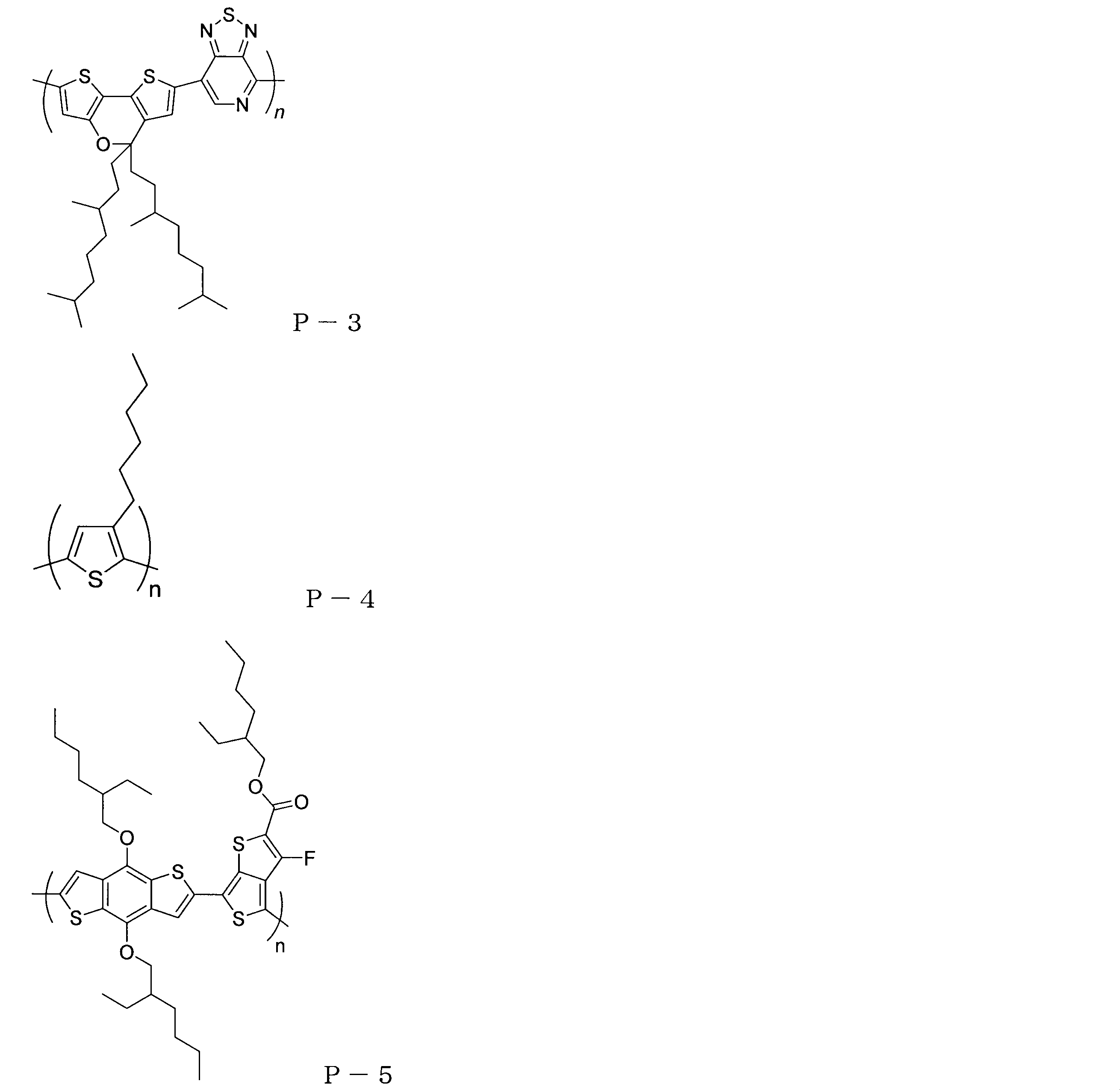
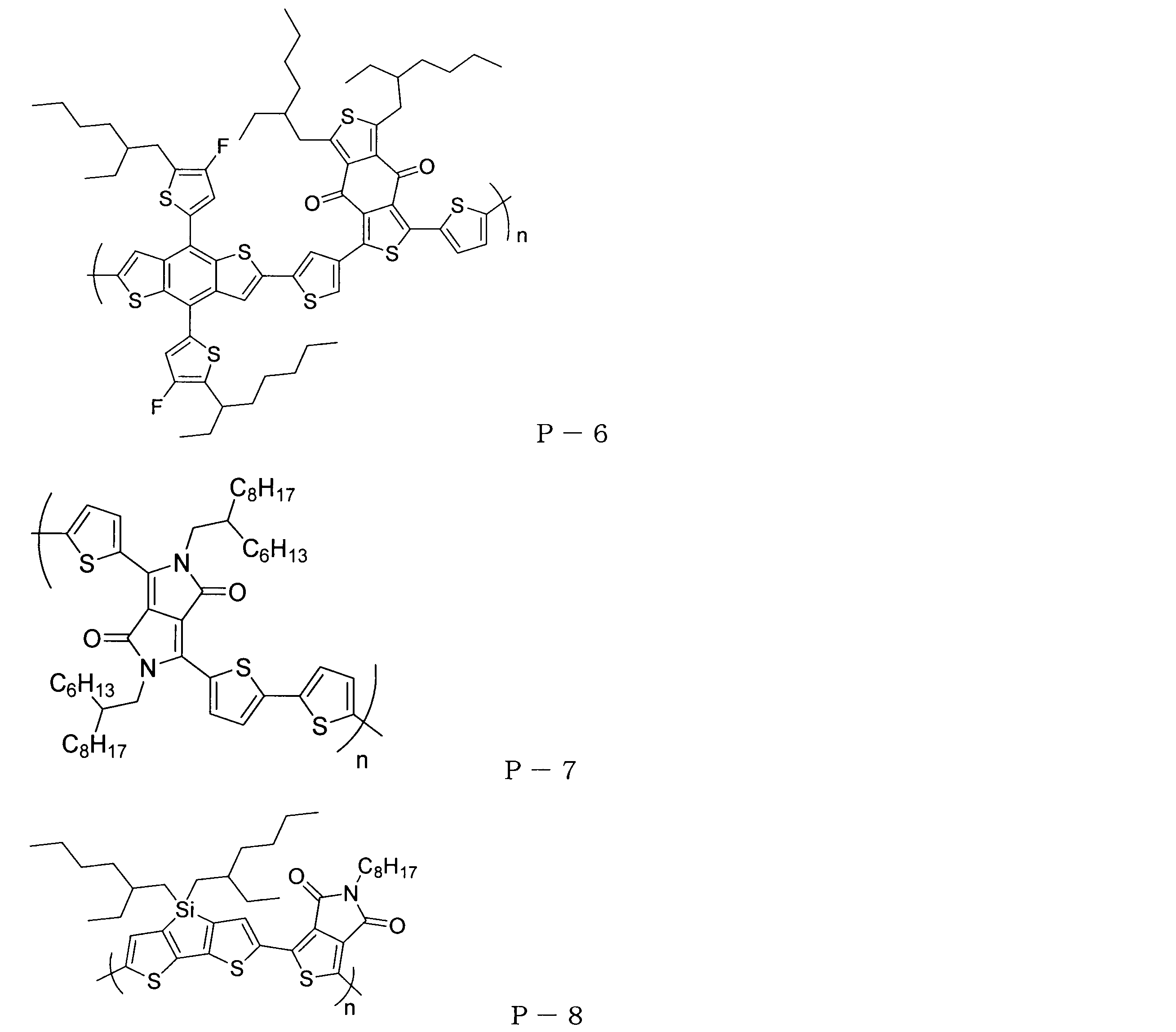
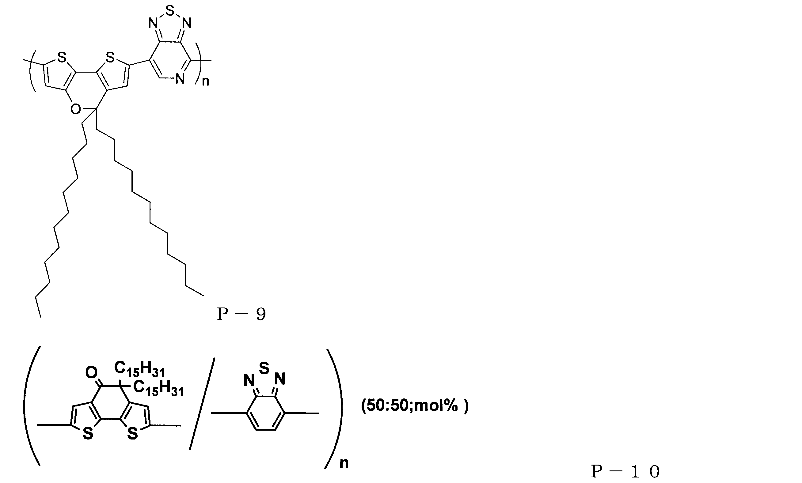

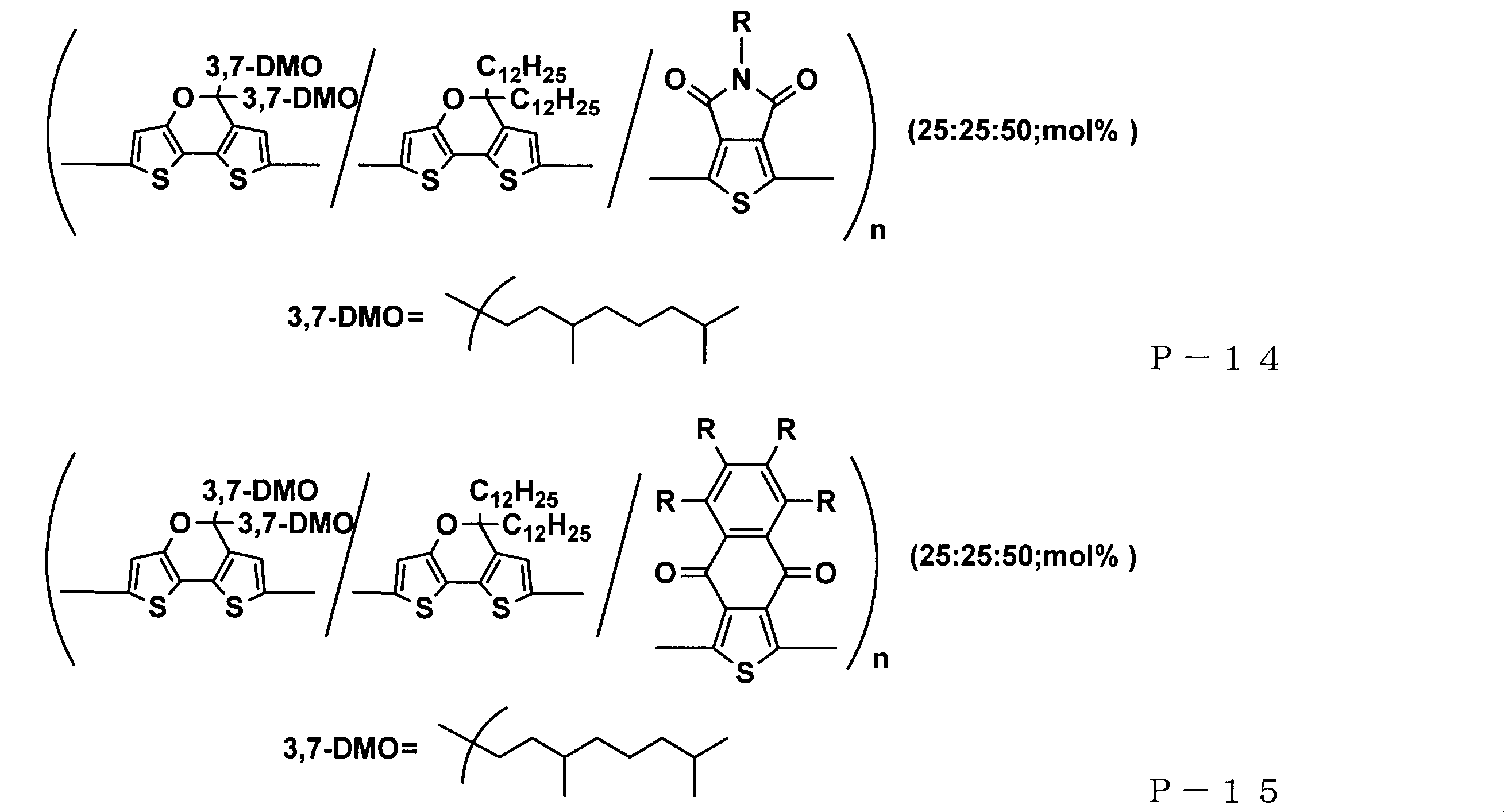
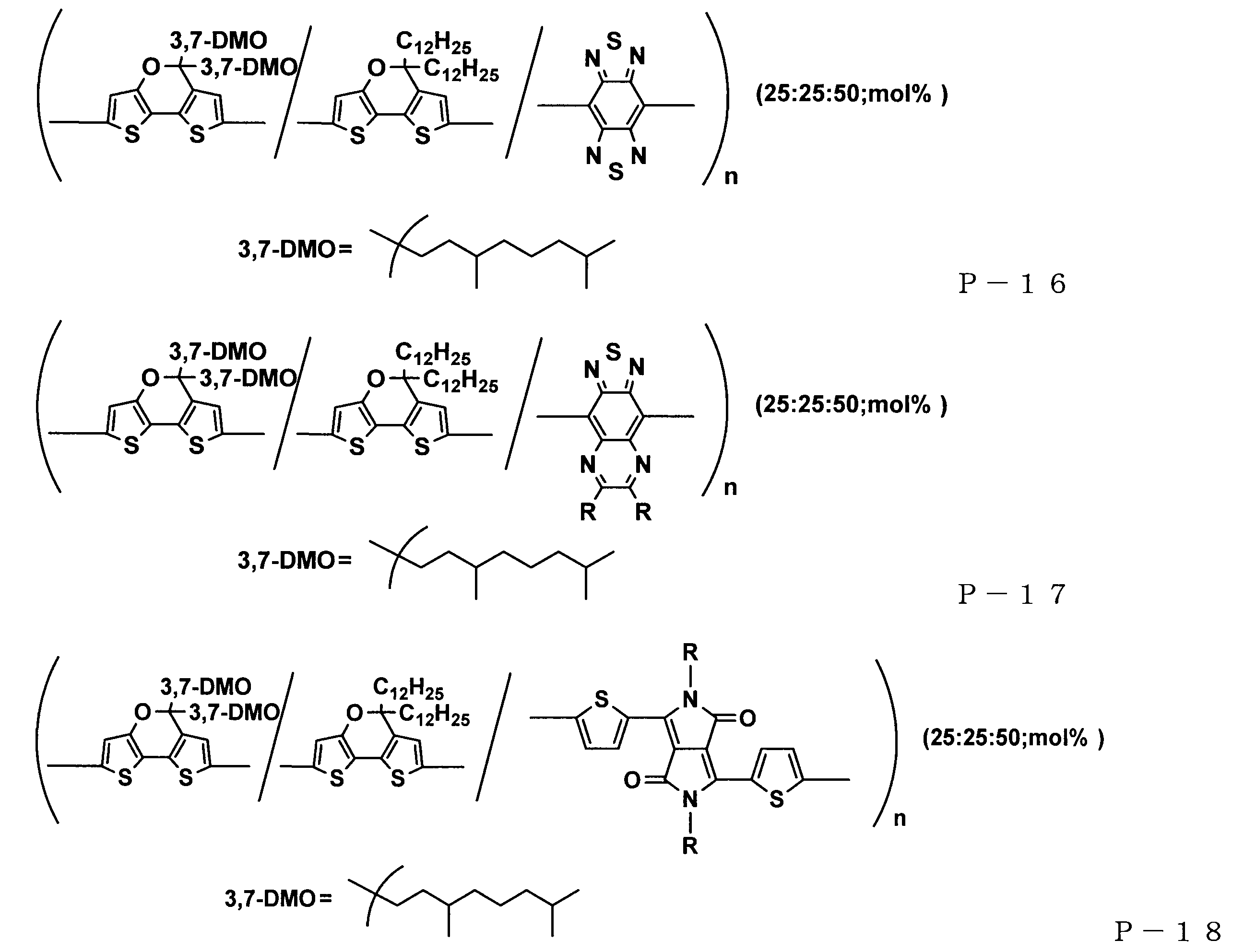
前記式中、Rは、前記定義のとおりである。複数あるRは、互いに同一であっても異なっていてもよい。
p型半導体材料として、上記例示の高分子化合物を用いれば、光電変換素子の製造工程又は光電変換素子が適用されるデバイスへの組み込み工程などにおける加熱処理に対EQEの低下を抑制するか又はEQEをより向上させることができ、光電変換素子の耐熱性を向上させることができる。
(中間層)
図1に示されるとおり、本実施形態の光電変換素子は、光電変換効率などの特性を向上させるための構成要素として、例えば、電荷輸送層(電子輸送層、正孔輸送層、電子注入層、正孔注入層)などの中間層(バッファー層)を備えていることが好ましい。
図1に示されるとおり、本実施形態の光電変換素子は、光電変換効率などの特性を向上させるための構成要素として、例えば、電荷輸送層(電子輸送層、正孔輸送層、電子注入層、正孔注入層)などの中間層(バッファー層)を備えていることが好ましい。
また、中間層に用いられる材料の例としては、カルシウムなどの金属、酸化モリブデン、酸化亜鉛などの無機酸化物半導体、及びPEDOT(ポリ(3,4-エチレンジオキシチオフェン))とPSS(ポリ(4-スチレンスルホネート))との混合物(PEDOT:PSS)が挙げられる。
図1に示されるように、光電変換素子は、陽極と活性層との間に、正孔輸送層を備えることが好ましい。正孔輸送層は、活性層から電極へと正孔を輸送する機能を有する。
陽極に接して設けられる正孔輸送層を、特に正孔注入層という場合がある。陽極に接して設けられる正孔輸送層(正孔注入層)は、陽極への正孔の注入を促進する機能を有する。正孔輸送層(正孔注入層)は、活性層に接していてもよい。
正孔輸送層は、正孔輸送性材料を含む。正孔輸送性材料の例としては、ポリチオフェン及びその誘導体、芳香族アミン化合物、芳香族アミン残基を有する構成単位を含む高分子化合物、CuSCN、CuI、NiO、酸化タングステン(WO3)及び酸化モリブデン(MoO3)が挙げられる。
中間層は、従来公知の任意好適な形成方法により形成することができる。中間層は、真空蒸着法や活性層の形成方法と同様の塗布法により形成することができる。
本実施形態にかかる光電変換素子は、中間層が電子輸送層であって、基板(支持基板)、陽極、正孔輸送層、活性層、電子輸送層、陰極がこの順に互いに接するように積層された構成を有することが好ましい。
図1に示されるように、本実施形態の光電変換素子は、陰極と活性層との間に、中間層として電子輸送層を備えていることが好ましい。電子輸送層は、活性層から陰極へと電子を輸送する機能を有する。電子輸送層は、陰極に接していてもよい。電子輸送層は活性層に接していてもよい。
陰極に接して設けられる電子輸送層を、特に電子注入層という場合がある。陰極に接して設けられる電子輸送層(電子注入層)は、活性層で発生した電子の陰極への注入を促進する機能を有する。
電子輸送層は、電子輸送性材料を含む。電子輸送性材料の例としては、ポリアルキレンイミン及びその誘導体、フルオレン構造を含む高分子化合物、カルシウムなどの金属、金属酸化物が挙げられる。
ポリアルキレンイミン及びその誘導体の例としては、エチレンイミン、プロピレンイミン、ブチレンイミン、ジメチルエチレンイミン、ペンチレンイミン、ヘキシレンイミン、ヘプチレンイミン、オクチレンイミンといった炭素原子数2~8のアルキレンイミン、特に炭素原子数2~4のアルキレンイミンの1種又は2種以上を常法により重合して得られるポリマー、ならびにそれらを種々の化合物と反応させて化学的に変性させたポリマーが挙げられる。ポリアルキレンイミン及びその誘導体としては、ポリエチレンイミン(PEI)及びエトキシ化ポリエチレンイミン(PEIE)が好ましい。
フルオレン構造を含む高分子化合物の例としては、ポリ[(9,9-ビス(3’-(N,N-ジメチルアミノ)プロピル)-2,7-フルオレン)-オルト-2,7-(9,9’-ジオクチルフルオレン)](PFN)及びPFN-P2が挙げられる。
金属酸化物の例としては、酸化亜鉛、ガリウムドープ酸化亜鉛、アルミニウムドープ酸化亜鉛、酸化チタン及び酸化ニオブが挙げられる。金属酸化物としては、亜鉛を含む金属酸化物が好ましく、中でも酸化亜鉛が好ましい。
その他の電子輸送性材料の例としては、ポリ(4-ビニルフェノール)、ペリレンジイミドが挙げられる。
(封止部材)
本実施形態の光電変換素子は、封止部材をさらに含み、かかる封止部材により封止された封止体とすることが好ましい。
封止部材は任意好適な従来公知の部材を用いることができる。封止部材の例としては、基板(封止基板)であるガラス基板とUV硬化性樹脂などの封止材(接着剤)との組合せが挙げられる。
本実施形態の光電変換素子は、封止部材をさらに含み、かかる封止部材により封止された封止体とすることが好ましい。
封止部材は任意好適な従来公知の部材を用いることができる。封止部材の例としては、基板(封止基板)であるガラス基板とUV硬化性樹脂などの封止材(接着剤)との組合せが挙げられる。
封止部材は、1層以上の層構造である封止層であってもよい。封止層を構成する層の例としては、ガスバリア層、ガスバリア性フィルムが挙げられる。
封止層は、水分を遮断する性質(水蒸気バリア性)又は酸素を遮断する性質(酸素バリア性)を有する材料により形成することが好ましい。封止層の材料として好適な材料の例としては、三フッ化ポリエチレン、ポリ三フッ化塩化エチレン(PCTFE)、ポリイミド、ポリカーボネート、ポリエチレンテレフタレート、脂環式ポリオレフィン、エチレン-ビニルアルコール共重合体などの有機材料、酸化ケイ素、窒化ケイ素、酸化アルミニウム、ダイヤモンドライクカーボンなどの無機材料などが挙げられる。
封止部材は、通常、光電変換素子が適用される、例えば下記適用例のデバイスに組み込まれる際において実施される加熱処理に耐え得る材料により構成される。
(光電変換素子の用途)
本実施形態の光電変換素子の用途としては、光検出素子、太陽電池が挙げられる。
より具体的には、本実施形態の光電変換素子は、電極間に電圧(逆バイアス電圧)を印加した状態で、透明又は半透明の電極側から光を照射することにより、光電流を流すことができ、光検出素子(光センサー)として動作させることができる。また、光検出素子を複数集積することによりイメージセンサーとして用いることもできる。このように本実施形態の光電変換素子は、特に光検出素子として好適に用いることができる。
本実施形態の光電変換素子の用途としては、光検出素子、太陽電池が挙げられる。
より具体的には、本実施形態の光電変換素子は、電極間に電圧(逆バイアス電圧)を印加した状態で、透明又は半透明の電極側から光を照射することにより、光電流を流すことができ、光検出素子(光センサー)として動作させることができる。また、光検出素子を複数集積することによりイメージセンサーとして用いることもできる。このように本実施形態の光電変換素子は、特に光検出素子として好適に用いることができる。
また、本実施形態の光電変換素子は、光が照射されることにより、電極間に光起電力を発生させることができ、太陽電池として動作させることができる。光電変換素子を複数集積することにより太陽電池モジュールとすることもできる。
(光電変換素子の適用例)
本実施形態にかかる光電変換素子は、光検出素子として、ワークステーション、パーソナルコンピュータ、携帯情報端末、入退室管理システム、デジタルカメラ、及び医療機器などの種々の電子装置が備える検出部に好適に適用することができる。
本実施形態にかかる光電変換素子は、光検出素子として、ワークステーション、パーソナルコンピュータ、携帯情報端末、入退室管理システム、デジタルカメラ、及び医療機器などの種々の電子装置が備える検出部に好適に適用することができる。
本実施形態の光電変換素子は、上記例示の電子装置が備える、例えば、X線撮像装置及びCMOSイメージセンサーなどの固体撮像装置用のイメージ検出部(例えば、X線センサーなどのイメージセンサー)、指紋検出部、顔検出部、静脈検出部及び虹彩検出部などの生体の一部分の所定の特徴を検出する生体情報認証装置の検出部(例えば、近赤外線センサー)、パルスオキシメータなどの光学バイオセンサーの検出部などに好適に適用することができる。
本実施形態の光電変換素子は、固体撮像装置用のイメージ検出部として、さらにはTime-of-flight(TOF)型距離測定装置(TOF型測距装置)に好適に適用することもできる。
TOF型測距装置では、光源からの放射光が測定対象物において反射された反射光を光電変換素子で受光させることにより距離を測定する。具体的には、光源から放射された照射光が測定対象物で反射して反射光として戻るまでの飛行時間を検出して測定対象物までの距離を求める。TOF型には、直接TOF方式と間接TOF方式とが存在する。直接TOF方式では光源から光を照射した時刻と反射光を光電変換素子で受光した時刻との差を直接計測し、間接TOF方式では飛行時間に依存した電荷蓄積量の変化を時間変化に換算することで距離を計測する。間接TOF方式で用いられる電荷蓄積により飛行時間を得る測距原理には、光源からの放射光と測定対象で反射される反射光との位相から飛行時間を求める連続波(特に正弦波)変調方式とパルス変調方式とがある。
以下、本実施形態にかかる光電変換素子が好適に適用され得る検出部のうち、固体撮像装置用のイメージ検出部及びX線撮像装置用のイメージ検出部、生体認証装置(例えば指紋認証装置や静脈認証装置など)のための指紋検出部及び静脈検出部、並びにTOF型測距装置(間接TOF方式)のイメージ検出部の構成例について、図面を参照して説明する。
(固体撮像装置用のイメージ検出部)
図2は、固体撮像装置用のイメージ検出部の構成例を模式的に示す図である。
図2は、固体撮像装置用のイメージ検出部の構成例を模式的に示す図である。
イメージ検出部1は、CMOSトランジスタ基板20と、CMOSトランジスタ基板20を覆うように設けられている層間絶縁膜30と、層間絶縁膜30上に設けられている、本発明の実施形態にかかる光電変換素子10と、層間絶縁膜30を貫通するように設けられており、CMOSトランジスタ基板20と光電変換素子10とを電気的に接続する層間配線部32と、光電変換素子10を覆うように設けられている封止層40と、封止層40上に設けられているカラーフィルター50とを備えている。
CMOSトランジスタ基板20は、従来公知の任意好適な構成を設計に応じた態様で備えている。
CMOSトランジスタ基板20は、基板の厚さ内に形成されたトランジスタ、コンデンサなどを含み、種々の機能を実現するためのCMOSトランジスタ回路(MOSトランジスタ回路)などの機能素子を備えている。
機能素子としては、例えば、フローティングディフュージョン、リセットトランジスタ、出力トランジスタ、選択トランジスタが挙げられる。
このような機能素子、配線などにより、CMOSトランジスタ基板20には、信号読み出し回路などが作り込まれている。
層間絶縁膜30は、例えば酸化シリコン、絶縁性樹脂などの従来公知の任意好適な絶縁性材料により構成することができる。層間配線部32は、例えば、銅、タングステンなどの従来公知の任意好適な導電性材料(配線材料)により構成することができる。層間配線部32は、例えば、配線層の形成と同時に形成されるホール内配線であっても、配線層とは別途形成される埋込みプラグであってもよい。
封止層40は、光電変換素子10を機能的に劣化させてしまうおそれのある酸素、水などの有害物質の浸透を防止又は抑制できることを条件として、従来公知の任意好適な材料により構成することができる。封止層40は、既に説明した封止部材17と同様の構成とすることができる。
カラーフィルター50としては、従来公知の任意好適な材料により構成され、かつイメージ検出部1の設計に対応した例えば原色カラーフィルターを用いることができる。また、カラーフィルター50としては、原色カラーフィルターと比較して、厚さを薄くすることができる補色カラーフィルターを用いることもできる。補色カラーフィルターとしては、例えば(イエロー、シアン、マゼンタ)の3種類、(イエロー、シアン、透明)の3種類、(イエロー、透明、マゼンタ)の3種類、及び(透明、シアン、マゼンタ)の3種類が組み合わされたカラーフィルターを用いることができる。これらは、カラー画像データを生成できることを条件として、光電変換素子10及びCMOSトランジスタ基板20の設計に対応した任意好適な配置とすることができる。
カラーフィルター50を介して光電変換素子10が受光した光は、光電変換素子10によって、受光量に応じた電気信号に変換され、電極を介して、光電変換素子10外に受光信号、すなわち撮像対象に対応する電気信号として出力される。
次いで、光電変換素子10から出力された受光信号は、層間配線部32を介して、CMOSトランジスタ基板20に入力され、CMOSトランジスタ基板20に作り込まれた信号読み出し回路により読み出され、図示しないさらなる任意好適な従来公知の機能部によって信号処理されることにより、撮像対象に基づく画像情報が生成される。
(指紋検出部)
図3は、表示装置に一体的に構成される指紋検出部の構成例を模式的に示す図である。
図3は、表示装置に一体的に構成される指紋検出部の構成例を模式的に示す図である。
携帯情報端末の表示装置2は、本発明の実施形態にかかる光電変換素子10を主たる構成要素として含む指紋検出部100と、当該指紋検出部100上に設けられ、所定の画像を表示する表示パネル部200とを備えている。
この構成例では、表示パネル部200の表示領域200aと一致する領域に指紋検出部100が設けられている。換言すると、指紋検出部100の上方に、表示パネル部200が一体的に積層されている。
表示領域200aのうちの一部の領域においてのみ指紋検出を行う場合には、当該一部の領域のみに対応させて指紋検出部100を設ければよい。
指紋検出部100は、本発明の実施形態にかかる光電変換素子10を本質的な機能を奏する機能部として含む。指紋検出部100は、図示されていない保護フィルム(protection film)、支持基板、封止基板、封止部材、バリアフィルム、バンドパスフィルター、赤外線カットフィルムなどの任意好適な従来公知の部材を所望の特性が得られるような設計に対応した態様で備え得る。指紋検出部100には、既に説明したイメージ検出部の構成を採用することもできる。
光電変換素子10は、表示領域200a内において、任意の態様で含まれ得る。例えば、複数の光電変換素子10が、マトリクス状に配置されていてもよい。
光電変換素子10は、既に説明したとおり、支持基板11に設けられており、支持基板11には、例えばマトリクス状に電極(陽極又は陰極)が設けられている。
光電変換素子10が受光した光は、光電変換素子10によって、受光量に応じた電気信号に変換され、電極を介して、光電変換素子10外に受光信号、すなわち撮像された指紋に対応する電気信号として出力される。
表示パネル部200は、この構成例では、タッチセンサーパネルを含む有機エレクトロルミネッセンス表示パネル(有機EL表示パネル)として構成されている。表示パネル部200は、例えば有機EL表示パネルの代わりに、バックライトなどの光源を含む液晶表示パネルなどの任意好適な従来公知の構成を有する表示パネルにより構成されていてもよい。
表示パネル部200は、既に説明した指紋検出部100上に設けられている。表示パネル部200は、有機エレクトロルミネッセンス素子(有機EL素子)220を本質的な機能を奏する機能部として含む。表示パネル部200は、さらに任意好適な従来公知のガラス基板といった基板(支持基板210又は封止基板240)、封止部材、バリアフィルム、円偏光板などの偏光板、タッチセンサーパネル230などの任意好適な従来公知の部材を所望の特性に対応した態様で備え得る。
以上説明した構成例において、有機EL素子220は、表示領域200aにおける画素の光源として用いられるとともに、指紋検出部100における指紋の撮像のための光源としても用いられる。
ここで、指紋検出部100の動作について簡単に説明する。
指紋認証の実行時には、表示パネル部200の有機EL素子220から放射される光を用いて指紋検出部100が指紋を検出する。具体的には、有機EL素子220から放射された光は、有機EL素子220と指紋検出部100の光電変換素子10との間に存在する構成要素を透過して、表示領域200a内である表示パネル部200の表面に接するように載置された手指の指先の皮膚(指表面)によって反射される。指表面によって反射された光のうちの少なくとも一部は、間に存在する構成要素を透過して光電変換素子10によって受光され、光電変換素子10の受光量に応じた電気信号に変換される。そして、変換された電気信号から、指表面の指紋についての画像情報が構成される。
指紋認証の実行時には、表示パネル部200の有機EL素子220から放射される光を用いて指紋検出部100が指紋を検出する。具体的には、有機EL素子220から放射された光は、有機EL素子220と指紋検出部100の光電変換素子10との間に存在する構成要素を透過して、表示領域200a内である表示パネル部200の表面に接するように載置された手指の指先の皮膚(指表面)によって反射される。指表面によって反射された光のうちの少なくとも一部は、間に存在する構成要素を透過して光電変換素子10によって受光され、光電変換素子10の受光量に応じた電気信号に変換される。そして、変換された電気信号から、指表面の指紋についての画像情報が構成される。
表示装置2を備える携帯情報端末は、従来公知の任意好適なステップにより、得られた画像情報と、予め記録されていた指紋認証用の指紋データとを比較して、指紋認証を行う。
(X線撮像装置用のイメージ検出部)
図4は、X線撮像装置用のイメージ検出部の構成例を模式的に示す図である。
図4は、X線撮像装置用のイメージ検出部の構成例を模式的に示す図である。
X線撮像装置用のイメージ検出部1は、CMOSトランジスタ基板20と、CMOSトランジスタ基板20を覆うように設けられている層間絶縁膜30と、層間絶縁膜30上に設けられている、本発明の実施形態にかかる光電変換素子10と、層間絶縁膜30を貫通するように設けられており、CMOSトランジスタ基板20と光電変換素子10とを電気的に接続する層間配線部32と、光電変換素子10を覆うように設けられている封止層40と、封止層40上に設けられているシンチレータ42とシンチレータ42を覆うように設けられている反射層44と、反射層44を覆うように設けられている保護層46とを備えている。
CMOSトランジスタ基板20は、従来公知の任意好適な構成を設計に応じた態様で備えている。
CMOSトランジスタ基板20は、基板の厚さ内に形成されたトランジスタ、コンデンサなどを含み、種々の機能を実現するためのCMOSトランジスタ回路(MOSトランジスタ回路)などの機能素子を備えている。
機能素子としては、例えば、フローティングディフュージョン、リセットトランジスタ、出力トランジスタ、選択トランジスタが挙げられる。
このような機能素子、配線などにより、CMOSトランジスタ基板20には、信号読み出し回路などが作り込まれている。
層間絶縁膜30は、例えば酸化シリコン、絶縁性樹脂などの従来公知の任意好適な絶縁性材料により構成することができる。層間配線部32は、例えば、銅、タングステンなどの従来公知の任意好適な導電性材料(配線材料)により構成することができる。層間配線部32は、例えば、配線層の形成と同時に形成されるホール内配線であっても、配線層とは別途形成される埋込みプラグであってもよい。
封止層40は、光電変換素子10を機能的に劣化させてしまうおそれのある酸素、水などの有害物質の浸透を防止又は抑制できることを条件として、従来公知の任意好適な材料により構成することができる。封止層40は、既に説明した封止部材17と同様の構成とすることができる。
シンチレータ42は、X線撮像装置用のイメージ検出部1の設計に対応した従来公知の任意好適な材料により構成することができる。シンチレータ42の好適な材料の例としては、CsI(ヨウ化セシウム)やNaI(ヨウ化ナトリウム)、ZnS(硫化亜鉛)、GOS(酸硫化ガドリニウム)、GSO(ケイ酸ガドリニウム)といった無機材料の無機結晶や、アントラセン、ナフタレン、スチルベンといった有機材料の有機結晶や、トルエン、キシレン、ジオキサンといった有機溶媒にジフェニルオキサゾール(PPO)やテルフェニル(TP)などの有機材料を溶解させた有機液体、キセノンやヘリウムといった気体、プラスチックなどを用いることができる。
上記の構成要素は、シンチレータ42が入射したX線を可視領域を中心とした波長を有する光に変換して画像データを生成できることを条件として、光電変換素子10及びCMOSトランジスタ基板20の設計に対応した任意好適な配置とすることができる。
反射層44は、シンチレータ42で変換された光を反射する。反射層44は、変換された光の損失を低減し、検出感度を増大させることができる。また、反射層44は、外部から直接的に入射する光を遮断することもできる。
保護層46は、シンチレータ42を機能的に劣化させてしまうおそれのある酸素、水などの有害物質の浸透を防止又は抑制できることを条件として、従来公知の任意好適な材料により構成することができる。
ここで、上記の構成を有するX線撮像装置用のイメージ検出部1の動作について簡単に説明する。
X線やγ線といった放射線エネルギーがシンチレータ42に入射すると、シンチレータ42は放射線エネルギーを吸収し、可視領域を中心とした紫外から赤外領域の波長の光(蛍光)に変換する。そして、シンチレータ42によって変換された光は、光電変換素子10によって受光される。
このように、シンチレータ42を介して光電変換素子10が受光した光は、光電変換素子10によって、受光量に応じた電気信号に変換され、電極を介して、光電変換素子10外に受光信号、すなわち撮像対象に対応する電気信号として出力される。検出対象である放射線エネルギー(X線)は、シンチレータ42側、光電変換素子10側のいずれから入射させてもよい。
次いで、光電変換素子10から出力された受光信号は、層間配線部32を介して、CMOSトランジスタ基板20に入力され、CMOSトランジスタ基板20に作り込まれた信号読み出し回路により読み出され、図示しないさらなる任意好適な従来公知の機能部によって信号処理されることにより、撮像対象に基づく画像情報が生成される。
(静脈検出部)
図5は、静脈認証装置用の静脈検出部の構成例を模式的に示す図である。
静脈認証装置用の静脈検出部300は、測定時において測定対象である手指(例、1以上の手指の指先、手指及び掌)が挿入される挿入部310を画成するカバー部306と、カバー部306に設けられており、測定対象に光を照射する光源部304と、光源部304から照射された光を測定対象を介して受光する光電変換素子10と、光電変換素子10を支持する支持基板11と、支持基板11と光電変換素子10を挟んで対向するように配置されており、所定の距離でカバー部306から離間して、カバー部306とともに挿入部310を画成するガラス基板302から構成されている。
この構成例では、光源部304は、光電変換素子10とは、使用時において測定対象を挟んで離間するように、カバー部306と一体的に構成されている透過型撮影方式を示しているが、光源部304は必ずしもカバー部306側に位置させる必要はない。
光源部304からの光を、測定対象に効率的に照射できることを条件として、例えば、光電変換素子10側から測定対象を照射する反射型撮影方式としてもよい。
静脈検出部300は、本発明の実施形態にかかる光電変換素子10を本質的な機能を奏する機能部として含む。静脈検出部300は、図示されていない保護フィルム(protection film)、封止部材、バリアフィルム、バンドパスフィルター、近赤外線透過フィルター、可視光カットフィルム、指置きガイドなどの任意好適な従来公知の部材を所望の特性が得られるような設計に対応した態様で備え得る。静脈検出部300には、既に説明したイメージ検出部1の構成を採用することもできる。
光電変換素子10は、任意の態様で含まれ得る。例えば、複数の光電変換素子10が、マトリクス状に配置されていてもよい。
光電変換素子10は、既に説明したとおり、支持基板11に設けられており、支持基板11には、例えばマトリクス状に電極(陽極又は陰極)が設けられている。
光電変換素子10が受光した光は、光電変換素子10によって、受光量に応じた電気信号に変換され、電極を介して、光電変換素子10外に受光信号、すなわち撮像された静脈に対応する電気信号として出力される。
静脈検出時(使用時)において、測定対象は、光電変換素子10側のガラス基板302に接触していても、接触していなくてもよい。
ここで、静脈検出部300の動作について簡単に説明する。
静脈検出時には、光源部304から放射される光を用いて静脈検出部300が測定対象の静脈パターンを検出する。具体的には、光源部304から放射された光は、測定対象を透過して光電変換素子10の受光量に応じた電気信号に変換される。そして、変換された電気信号から、測定対象の静脈パターンの画像情報が構成される。
静脈検出時には、光源部304から放射される光を用いて静脈検出部300が測定対象の静脈パターンを検出する。具体的には、光源部304から放射された光は、測定対象を透過して光電変換素子10の受光量に応じた電気信号に変換される。そして、変換された電気信号から、測定対象の静脈パターンの画像情報が構成される。
静脈認証装置では、従来公知の任意好適なステップにより、得られた画像情報と、予め記録されていた静脈認証用の静脈データとを比較して、静脈認証が行われる。
(TOF型測距装置用イメージ検出部)
図6は、間接方式のTOF型測距装置用イメージ検出部の構成例を模式的に示す図である。
図6は、間接方式のTOF型測距装置用イメージ検出部の構成例を模式的に示す図である。
TOF型測距装置用イメージ検出部400は、CMOSトランジスタ基板20と、CMOSトランジスタ基板20を覆うように設けられている層間絶縁膜30と、層間絶縁膜30上に設けられている、本発明の実施形態にかかる光電変換素子10と、光電変換素子10を挟むように離間して配置されている2つの浮遊拡散層402と、光電変換素子10と浮遊拡散層402を覆うように設けられている絶縁層401と、絶縁層401上に設けられており、互いに離間して配置されている2つのフォトゲート404とを備えている。離間した2つのフォトゲート404の間隙からは絶縁層401の一部分が露出しており、残余の領域は遮光部406により遮光されている。CMOSトランジスタ基板20と浮遊拡散層402とは層間絶縁膜30を貫通するように設けられている層間配線部32によって電気的に接続されている。
絶縁層401は、この構成例では、酸化シリコンにより構成されるフィールド酸化膜などの従来公知の任意好適な構成とすることができる。
フォトゲート404は、例えばポリシリコンなどの従来公知の任意好適な材料により構成することができる。
TOF型測距装置用イメージ検出部400は、本発明の実施形態にかかる光電変換素子10を本質的な機能を奏する機能部として含む。TOF型測距装置用イメージ検出部400は、図示されていない保護フィルム(protection film)、支持基板、封止基板、封止部材、バリアフィルム、バンドパスフィルター、赤外線カットフィルムなどの任意好適な従来公知の部材を所望の特性が得られるような設計に対応した態様で備え得る。
ここで、TOF型測距装置用イメージ検出部400の動作について簡単に説明する。
光源から光が照射され、光源からの光が測定対象より反射され、反射光を光電変換素子10で受光する。光電変換素子10と浮遊拡散層402との間には2つのフォトゲート404が設けられており、交互にパルスを加えることによって、光電変換素子10によって発生した信号電荷を2つの浮遊拡散層402のいずれかに転送し、浮遊拡散層402に電荷が蓄積される。2つのフォトゲート404を開くタイミングに対して、光パルスが等分にまたがるように到来すると、2つの浮遊拡散層402に蓄積される電荷量は等量になる。一方のフォトゲート404に光パルスが到達するタイミングに対して、他方のフォトゲート404に光パルスが遅れて到来すると、2つの浮遊拡散層402に蓄積される電荷量に差が生じる。
光源から光が照射され、光源からの光が測定対象より反射され、反射光を光電変換素子10で受光する。光電変換素子10と浮遊拡散層402との間には2つのフォトゲート404が設けられており、交互にパルスを加えることによって、光電変換素子10によって発生した信号電荷を2つの浮遊拡散層402のいずれかに転送し、浮遊拡散層402に電荷が蓄積される。2つのフォトゲート404を開くタイミングに対して、光パルスが等分にまたがるように到来すると、2つの浮遊拡散層402に蓄積される電荷量は等量になる。一方のフォトゲート404に光パルスが到達するタイミングに対して、他方のフォトゲート404に光パルスが遅れて到来すると、2つの浮遊拡散層402に蓄積される電荷量に差が生じる。
浮遊拡散層402に蓄積された電荷量の差は、光パルスの遅延時間に依存する。測定対象までの距離Lは、光の往復時間tdと光の速度cを用いてL=(1/2)ctdの関係にあるので、遅延時間が2つの浮遊拡散層402の電荷量の差から推定できれば、測定対象までの距離を求めることができる。
光電変換素子10が受光した光の受光量は、2つの浮遊拡散層402に蓄積される電荷量の差として電気信号に変換され、光電変換素子10外に受光信号、すなわち測定対象に対応する電気信号として出力される。
次いで、浮遊拡散層402から出力された受光信号は、層間配線部32を介して、CMOSトランジスタ基板20に入力され、CMOSトランジスタ基板20に作り込まれた信号読み出し回路により読み出され、図示しないさらなる任意好適な従来公知の機能部によって信号処理されることにより、測定対象に基づく距離情報が生成される。
本実施形態の光電変換素子が適用される上記適用例にかかるデバイスに組み込まれる工程においては、例えば、配線基板などに搭載するためのリフロー工程などの加熱処理が行われる場合がある。例えば、イメージセンサーを製造するにあたり、200℃以上の加熱温度にて50分間程度、光電変換素子が加熱される処理を含む工程が実施される場合がある。
本実施形態の光電変換素子によれば、活性層の材料として、既に説明した本実施形態の化合物(n型半導体材料である非フラーレン化合物)と、既に説明したp型半導体材料が用いられる。これにより、活性層の形成工程において(詳細については後述する。)、活性層の形成後における光電変換素子の製造工程において、又は製造された光電変換素子をイメージセンサーや生体認証装置に組み込む工程などにおいて、200℃以上の加熱温度にて加熱される処理が行われたとしても、EQEの低下を抑制するか又はEQEをより向上させることができ、耐熱性を効果的に向上させることができる。
具体的には、EQEについては、光電変換素子の製造方法の活性層の形成工程におけるプリベーク工程の加熱温度を100℃とした光電変換素子におけるEQEの値を基準として、ポストベーク工程の加熱温度をより高温に変更した光電変換素子におけるEQEの値で除算することにより規格化して得た値(以下、「EQEheat/EQE100℃」という。)が0.80以上が好ましく、0.85以上がより好ましく、1.0以上であることがさらに好ましい。
4.光電変換素子の製造方法
本実施形態の光電変換素子の製造方法は、特に限定されない。本実施形態の光電変換素子は、構成要素を形成するにあたり選択された材料に好適な形成方法を組み合わせることにより製造することができる。
本実施形態の光電変換素子の製造方法は、特に限定されない。本実施形態の光電変換素子は、構成要素を形成するにあたり選択された材料に好適な形成方法を組み合わせることにより製造することができる。
本実施形態の光電変換素子の製造方法には、200℃以上の加熱温度で加熱される処理を含む工程が含まれうる。より具体的には、活性層が、200℃以上の加熱温度で加熱される処理を含む工程により形成され、及び/又は活性層が形成される工程よりも後に、200℃以上の加熱温度で加熱される処理を含む工程が含まれうる。
以下、本発明の実施形態として、基板(支持基板)、陽極、正孔輸送層、活性層、電子輸送層、陰極がこの順に互いに接する構成を有する光電変換素子の製造方法について説明する。
(基板を用意する工程)
本工程では、例えば陽極が設けられた支持基板を用意する。また、既に説明した電極の材料により形成された導電性の薄膜が設けられた基板を市場より入手し、必要に応じて、導電性の薄膜をパターニングして陽極を形成することにより、陽極が設けられた支持基板を用意することができる。
本工程では、例えば陽極が設けられた支持基板を用意する。また、既に説明した電極の材料により形成された導電性の薄膜が設けられた基板を市場より入手し、必要に応じて、導電性の薄膜をパターニングして陽極を形成することにより、陽極が設けられた支持基板を用意することができる。
本実施形態にかかる光電変換素子の製造方法において、支持基板上に陽極を形成する場合の陽極の形成方法は特に限定されない。陽極は、既に説明した材料を、真空蒸着法、スパッタリング法、イオンプレーティング法、めっき法、塗布法などの従来公知の任意好適な方法によって、陽極を形成すべき構成(例、支持基板、活性層、正孔輸送層)上に形成することができる。
(正孔輸送層の形成工程)
光電変換素子の製造方法は、活性層と陽極との間に設けられる正孔輸送層(正孔注入層)を形成する工程を含んでいてもよい。
光電変換素子の製造方法は、活性層と陽極との間に設けられる正孔輸送層(正孔注入層)を形成する工程を含んでいてもよい。
正孔輸送層の形成方法は特に限定されない。正孔輸送層の形成工程をより簡便にする観点からは、従来公知の任意好適な塗布法によって正孔輸送層を形成することが好ましい。
正孔輸送層は、例えば、既に説明した正孔輸送層の材料と溶媒とを含む塗布液を用いる塗布法や真空蒸着法により形成することができる。
正孔輸送層は、例えば、既に説明した正孔輸送層の材料と溶媒とを含む塗布液を用いる塗布法や真空蒸着法により形成することができる。
(活性層の形成工程)
本実施形態の光電変換素子の製造方法においては、正孔輸送層上に活性層が形成される。主要な構成要素である活性層は、任意好適な従来公知の形成工程により形成することができる。本実施形態において、活性層は、インク(塗布液)を用いる塗布法により製造することが好ましい。
本実施形態の光電変換素子の製造方法においては、正孔輸送層上に活性層が形成される。主要な構成要素である活性層は、任意好適な従来公知の形成工程により形成することができる。本実施形態において、活性層は、インク(塗布液)を用いる塗布法により製造することが好ましい。
以下、本発明の光電変換素子の主たる構成要素である活性層の形成工程が含む工程(i)及び工程(ii)について説明する。
工程(i)
インクを塗布対象に塗布する方法としては、任意好適な塗布法を用いることができる。
塗布法としては、スリットコート法、ナイフコート法、スピンコート法、マイクログラビアコート法、グラビアコート法、バーコート法、インクジェット印刷法、ノズルコート法、又はキャピラリーコート法が好ましく、スリットコート法、スピンコート法、キャピラリーコート法、又はバーコート法がより好ましく、スリットコート法、又はスピンコート法がさらに好ましい。
インクを塗布対象に塗布する方法としては、任意好適な塗布法を用いることができる。
塗布法としては、スリットコート法、ナイフコート法、スピンコート法、マイクログラビアコート法、グラビアコート法、バーコート法、インクジェット印刷法、ノズルコート法、又はキャピラリーコート法が好ましく、スリットコート法、スピンコート法、キャピラリーコート法、又はバーコート法がより好ましく、スリットコート法、又はスピンコート法がさらに好ましい。
本実施形態の光電変換素子の製造方法に用いられるインクは、p型半導体材料と、n型半導体材料とを含み、該n型半導体材料として、既に説明した本実施形態の化合物を含む、組成物と、溶媒とを含む。
よって、本実施形態のインクは光電変換素子の活性層形成用のインクであることが好ましい。以下、本実施形態の活性層形成用のインクについて説明する。なお、本実施形態の活性層形成用のインクはバルクヘテロジャンクション型活性層の形成用のインクである。
よって、活性層形成用のインクは、既に説明したp型半導体材料とn型半導体材料として、既に説明した本実施形態の化合物を含む組成物を含む。本実施形態の活性層形成用のインクは、当該組成物と、1種又は2種以上の溶媒とを含む。
よって、活性層形成用のインクは、既に説明したp型半導体材料とn型半導体材料として、既に説明した本実施形態の化合物を含む組成物を含む。本実施形態の活性層形成用のインクは、当該組成物と、1種又は2種以上の溶媒とを含む。
本実施形態の活性層形成用のインクによれば、p型半導体材料と、「本実施形態の化合物」とを含むことにより、光電変換素子の製造工程又は光電変換素子が適用されるデバイスへの組み込み工程などにおける加熱処理に対するEQEの低下を抑制するか又はEQEをより向上させることができ、耐熱性を向上させることができる。
本実施形態にかかる活性層形成用のインクは、活性層が形成できることを条件として、特に限定されない。溶媒としては、例えば、後述する第1溶媒と第2溶媒と組み合わせた混合溶媒を用いることができる。具体的には、活性層形成用のインクが2種以上の溶媒を含む場合、主たる成分である主溶媒(第1溶媒)と、溶解性の向上などのために添加されるその他の添加溶媒(第2溶媒)とを含むことが好ましい。しかしながら、第1溶媒のみを用いてもよい。
以下、本実施形態の活性層形成用のインクに好適に用いることができる第1溶媒及び第2溶媒とこれらの組合せについて説明する。
(1)第1溶媒
第1溶媒としては、p型半導体材料が溶解可能である溶媒が好ましい。本実施形態の第1溶媒は、芳香族炭化水素である。
第1溶媒としては、p型半導体材料が溶解可能である溶媒が好ましい。本実施形態の第1溶媒は、芳香族炭化水素である。
第1溶媒である芳香族炭化水素としては、例えば、トルエン、キシレン(例、o-キシレン、m-キシレン、p-キシレン)、o-ジクロロベンゼン、トリメチルベンゼン(例、メシチレン、1,2,4-トリメチルベンゼン(プソイドクメン))、ブチルベンゼン(例、n-ブチルベンゼン、sec-ブチルベンゼン、tert-ブチルベンゼン)、メチルナフタレン(例、1-メチルナフタレン)、テトラリン及びインダンが挙げられる。
第1溶媒は、1種の芳香族炭化水素から構成されていても、2種以上の芳香族炭化水素から構成されていてもよい。第1溶媒は、好ましくは1種の芳香族炭化水素から構成される。
第1溶媒は、好ましくはトルエン、o-キシレン、m-キシレン、p-キシレン、メシチレン、o-ジクロロベンゼン、1,2,4-トリメチルベンゼン、n-ブチルベンゼン、sec-ブチルベンゼン、tert-ブチルベンゼン、メチルナフタレン、テトラリン及びインダンからなる群から選択される1種以上であり、より好ましくはトルエン、o-キシレン、m-キシレン、p-キシレン、o-ジクロロベンゼン、メシチレン、1,2,4-トリメチルベンゼン、n-ブチルベンゼン、sec-ブチルベンゼン、tert-ブチルベンゼン、メチルナフタレン、テトラリン、又はインダンである。
(2)第2溶媒
第2溶媒は、製造工程の実施をより容易にし、光電変換素子の特性をより向上させる観点から選択される溶媒である。第2溶媒としては、例えば、アセトン、メチルエチルケトン、シクロヘキサノン、アセトフェノン、プロピオフェノンなどのケトン溶媒、酢酸エチル、酢酸ブチル、酢酸フェニル、エチルセルソルブアセテート、安息香酸メチル、安息香酸ブチル及び安息香酸ベンジルなどのエステル溶媒が挙げられる。
第2溶媒は、製造工程の実施をより容易にし、光電変換素子の特性をより向上させる観点から選択される溶媒である。第2溶媒としては、例えば、アセトン、メチルエチルケトン、シクロヘキサノン、アセトフェノン、プロピオフェノンなどのケトン溶媒、酢酸エチル、酢酸ブチル、酢酸フェニル、エチルセルソルブアセテート、安息香酸メチル、安息香酸ブチル及び安息香酸ベンジルなどのエステル溶媒が挙げられる。
第2溶媒は、例えば、暗電流をより低減する観点から、アセトフェノン、プロピオフェノン、安息香酸ブチル又は安息香酸メチルを用いることが好ましい。
(3)第1溶媒及び第2溶媒の組合せ
第1溶媒及び第2溶媒の好適な組合せの例としては、テトラリンと安息香酸エチル、テトラリンと安息香酸プロピル及びテトラリンと安息香酸ブチルとの組合せ、より好ましくはテトラリンと安息香酸ブチルとの組合せが挙げられる。
第1溶媒及び第2溶媒の好適な組合せの例としては、テトラリンと安息香酸エチル、テトラリンと安息香酸プロピル及びテトラリンと安息香酸ブチルとの組合せ、より好ましくはテトラリンと安息香酸ブチルとの組合せが挙げられる。
(4)第1溶媒及び第2溶媒の重量比
主溶媒である第1溶媒の添加溶媒である第2溶媒に対する重量比(第1溶媒:第2溶媒)は、p型半導体材料及びn型半導体材料の溶解性をより向上させる観点から、85:15~99:1の範囲とすることが好ましい。
主溶媒である第1溶媒の添加溶媒である第2溶媒に対する重量比(第1溶媒:第2溶媒)は、p型半導体材料及びn型半導体材料の溶解性をより向上させる観点から、85:15~99:1の範囲とすることが好ましい。
(5)任意の他の溶媒
溶媒は、第1溶媒及び第2溶媒以外の任意の他の溶媒を含んでいてもよい。インクに含まれる全溶媒の合計重量を100質量%としたときに、任意の他の溶媒の含有率は、好ましくは5質量%以下であり、より好ましくは3質量%以下であり、さらに好ましくは1質量%以下である。任意の他の溶媒としては、第2溶媒より沸点が高い溶媒が好ましい。
溶媒は、第1溶媒及び第2溶媒以外の任意の他の溶媒を含んでいてもよい。インクに含まれる全溶媒の合計重量を100質量%としたときに、任意の他の溶媒の含有率は、好ましくは5質量%以下であり、より好ましくは3質量%以下であり、さらに好ましくは1質量%以下である。任意の他の溶媒としては、第2溶媒より沸点が高い溶媒が好ましい。
(6)任意の成分
インクには、第1溶媒、第2溶媒、p型半導体材料及びn型半導体材料の他に、本発明の目的及び効果を損なわない限度において、界面活性剤、紫外線吸収剤、酸化防止剤、吸収した光により電荷を発生させる機能を増感するための増感剤、紫外線からの安定性を増すための光安定剤といった任意の成分が含まれていてもよい。
インクには、第1溶媒、第2溶媒、p型半導体材料及びn型半導体材料の他に、本発明の目的及び効果を損なわない限度において、界面活性剤、紫外線吸収剤、酸化防止剤、吸収した光により電荷を発生させる機能を増感するための増感剤、紫外線からの安定性を増すための光安定剤といった任意の成分が含まれていてもよい。
(7)p型半導体材料及びn型半導体材料の濃度
インク(組成物)におけるp型半導体材料及びn型半導体材料の濃度は、溶媒に対する溶解度なども考慮して、本発明の目的を損なわない範囲で任意好適な濃度とすることができる。
インク(組成物)におけるp型半導体材料及びn型半導体材料の濃度は、溶媒に対する溶解度なども考慮して、本発明の目的を損なわない範囲で任意好適な濃度とすることができる。
インクにおける「p型半導体材料」の「n型半導体材料」に対する重量比(重合体/非フラーレン化合物)は、通常1/0.1から1/10の範囲であり、好ましくは1/0.5から1/2の範囲であり、より好ましくは1/1.5である。
インクにおける「p型半導体材料」及び「n型半導体材料」の合計の濃度は、通常0.01質量%以上であり、0.02質量%以上がより好ましく、0.25質量%以上がさらに好ましい。また、インクにおける「p型半導体材料」及び「n型半導体材料」の合計の濃度は、通常20質量%以下であり、10質量%以下であることが好ましく、7.50質量%以下であることがより好ましい。
インクにおける「p型半導体材料」の濃度は、通常0.01質量%以上であり、0.02質量%以上がより好ましく、0.10質量%以上がさらに好ましい。また、インクにおける「p型半導体材料」の濃度は、通常10質量%以下であり、5.00質量%以下がより好ましく、3.00質量%以下がさらに好ましい。
インクにおける「n型半導体材料」の濃度は、通常0.01質量%以上であり、0.02質量%以上がより好ましく、0.15質量%以上がさらに好ましい。また、インクにおける「n型半導体材料」の濃度は、通常10質量%以下であり、5質量%以下がより好ましく、4.50質量%以下がさらに好ましい。
(8)インクの調製
インクは、公知の方法により調製することができる。例えば、第1溶媒、又は第1溶媒及び第2溶媒を混合して混合溶媒を調製し、得られた混合溶媒にp型半導体材料及びn型半導体材料を添加する方法、第1溶媒にp型半導体材料を添加し、第2溶媒にn型半導体材料を添加してから、各材料が添加された第1溶媒及び第2溶媒を混合する方法などにより、調製することができる。
インクは、公知の方法により調製することができる。例えば、第1溶媒、又は第1溶媒及び第2溶媒を混合して混合溶媒を調製し、得られた混合溶媒にp型半導体材料及びn型半導体材料を添加する方法、第1溶媒にp型半導体材料を添加し、第2溶媒にn型半導体材料を添加してから、各材料が添加された第1溶媒及び第2溶媒を混合する方法などにより、調製することができる。
第1溶媒及び第2溶媒とp型半導体材料及びn型半導体材料とを、溶媒の沸点以下の温度まで加温して混合してもよい。
第1溶媒及び第2溶媒とp型半導体材料及びn型半導体材料とを混合した後、得られた混合物をフィルターを用いてろ過し、得られたろ液をとして用いてもよい。フィルターとしては、例えば、ポリテトラフルオロエチレン(PTFE)などのフッ素樹脂で形成されたフィルターを用いることができる。
活性層形成用のインクは、光電変換素子及びその製造方法に応じて選択された塗布対象に塗布される。活性層形成用のインクは、光電変換素子の製造工程において、光電変換素子が有する機能層であって、活性層が存在し得る機能層に塗布されうる。よって、活性層形成用のインクの塗布対象は、製造される光電変換素子の層構成及び層形成の順序によって異なる。例えば、光電変換素子が、基板、陽極、正孔輸送層、活性層、電子輸送層、陰極が積層された層構成を有しており、より左側に記載された層が先に形成される場合、活性層形成用のインクの塗布対象は、正孔輸送層となる。また、例えば、光電変換素子が、基板、陰極、電子輸送層、活性層、正孔輸送層、陽極が積層された層構成を有しており、より左側に記載された層が先に形成される場合、活性層形成用のインクの塗布対象は、電子輸送層となる。
工程(ii)
インクの塗膜から、溶媒を除去する方法、すなわち塗膜から溶媒を除去して固化する方法としては、任意好適な方法を用いることができる。溶媒を除去する方法の例としては、窒素ガスなどの不活性ガス雰囲気下でホットプレートを用いて直接的に加熱する方法、熱風乾燥法、赤外線加熱乾燥法、フラッシュランプアニール乾燥法、減圧乾燥法などの乾燥法が挙げられる。
インクの塗膜から、溶媒を除去する方法、すなわち塗膜から溶媒を除去して固化する方法としては、任意好適な方法を用いることができる。溶媒を除去する方法の例としては、窒素ガスなどの不活性ガス雰囲気下でホットプレートを用いて直接的に加熱する方法、熱風乾燥法、赤外線加熱乾燥法、フラッシュランプアニール乾燥法、減圧乾燥法などの乾燥法が挙げられる。
本実施形態の光電変換素子の製造方法においては、工程(ii)は、溶媒を揮発させて除去するための工程であって、プリベーク工程(第1の加熱処理工程)とも称される。
プリベーク工程及びポストベーク工程の実施条件、すなわち加熱温度、加熱処理時間などの条件については、用いられるインクの組成、溶媒の沸点などを考慮して、任意好適な条件とすることができる。
本実施形態の光電変換素子の製造方法においては、具体的には、例えば、窒素ガス雰囲気下でホットプレートを用いて、プリベーク工程及びポストベーク工程を実施することができる。
プリベーク工程における加熱温度は、通常100℃程度である。しかしながら、本実施形態の光電変換素子の製造方法においては、活性層の材料として、既に説明したp型半導体材料と既に説明した本実施形態の化合物をn型半導体材料として含む結果として、プリベーク工程及び/又はポストベーク工程における加熱温度をより高めることができる。具体的には、プリベーク工程及び/又はポストベーク工程における加熱温度を、好ましくは200℃以上、さらには220℃以上とすることができる。加熱温度の上限は、好ましくは280℃以下であり、より好ましくは250℃以下である。
プリベーク工程及びポストベーク工程における合計の加熱処理時間は、例えば1時間とすることができる。
プリベーク工程における加熱温度とポストベーク工程における加熱温度とは同一であっても異なっていてもよい。
加熱処理時間は例えば10分間以上とすることができる。加熱処理時間の上限値は特に限定されないが、タクトタイム等を考慮し、例えば4時間とすることができる。
活性層の厚さは、塗布液中の固形分濃度、上記工程(i)及び/又は工程(ii)の条件を適宜調整することにより、任意好適な所望の厚さとすることができる。
活性層を形成する工程は、前記工程(i)及び工程(ii)以外に、本発明の目的及び効果を損なわないことを条件としてその他の工程を含んでいてもよい。
本実施形態の光電変換素子の製造方法は、複数の活性層を含む光電変換素子を製造する方法であってもよく、工程(i)及び工程(ii)が複数回繰り返される方法であってもよい。
(電子輸送層の形成工程)
本実施形態の光電変換素子の製造方法は、活性層上に設けられた電子輸送層(電子注入層)を形成する工程を含んでいる。
本実施形態の光電変換素子の製造方法は、活性層上に設けられた電子輸送層(電子注入層)を形成する工程を含んでいる。
電子輸送層の形成方法は特に限定されない。電子輸送層の形成工程をより簡便にする観点からは、従来公知の任意好適な真空蒸着法によって電子輸送層を形成することが好ましい。
(陰極の形成工程)
陰極の形成方法は特に限定されない。陰極は、例えば、上記例示の電極の材料を、塗布法、真空蒸着法、スパッタリング法、イオンプレーティング法、めっき法など従来公知の任意好適な方法によって、電子輸送層上に形成することができる。以上の工程により、本実施形態の光電変換素子が製造される。
陰極の形成方法は特に限定されない。陰極は、例えば、上記例示の電極の材料を、塗布法、真空蒸着法、スパッタリング法、イオンプレーティング法、めっき法など従来公知の任意好適な方法によって、電子輸送層上に形成することができる。以上の工程により、本実施形態の光電変換素子が製造される。
(封止体の形成工程)
封止体の形成にあたり、本実施形態では、従来公知の任意好適な封止材(接着剤)及び基板(封止基板)を用いる。具体的には、製造された光電変換素子の周辺を囲むように、支持基板上に、例えばUV硬化性樹脂などの封止材を塗布した後、封止材により隙間なく貼り合わせた後、UV光の照射などの選択された封止材に好適な方法を用いて支持基板と封止基板との間隙に光電変換素子を封止することにより、光電変換素子の封止体を得ることができる。
封止体の形成にあたり、本実施形態では、従来公知の任意好適な封止材(接着剤)及び基板(封止基板)を用いる。具体的には、製造された光電変換素子の周辺を囲むように、支持基板上に、例えばUV硬化性樹脂などの封止材を塗布した後、封止材により隙間なく貼り合わせた後、UV光の照射などの選択された封止材に好適な方法を用いて支持基板と封止基板との間隙に光電変換素子を封止することにより、光電変換素子の封止体を得ることができる。
5.イメージセンサー、生体認証装置の製造方法
本実施形態の光電変換素子である特に光検出素子は、上記のとおり、イメージセンサー、生体認証装置(指紋認証装置、静脈認証装置)に組み込まれて機能しうる。
本実施形態の光電変換素子である特に光検出素子は、上記のとおり、イメージセンサー、生体認証装置(指紋認証装置、静脈認証装置)に組み込まれて機能しうる。
このようなイメージセンサー、生体認証装置は、200℃以上の加熱温度で光電変換素子(光電変換素子の封止体)が加熱される処理を含む工程を含む製造方法により製造され得る。
具体的には、光電変換素子をイメージセンサーや生体認証装置に組み込む工程を行うにあたって、例えば、配線基板に搭載する際に行われるリフロー工程などが行われることにより、200℃以上、さらには220℃以上の加熱温度で加熱される処理が行われ得る。
しかしながら、本実施形態の光電変換素子によれば、活性層の材料として、既に説明したn型半導体材料が用いられるため、組み込まれた光電変換素子のEQEの低下を抑制するか又はEQEをより向上させ、さらには暗電流の増加を抑制するか又は暗電流をより低下させることができ、耐熱性を効果的に向上させることができるため、製造されるイメージセンサー、生体認証装置における検出精度などの特性を向上することができる。
しかしながら、本実施形態の光電変換素子によれば、活性層の材料として、既に説明したn型半導体材料が用いられるため、組み込まれた光電変換素子のEQEの低下を抑制するか又はEQEをより向上させ、さらには暗電流の増加を抑制するか又は暗電流をより低下させることができ、耐熱性を効果的に向上させることができるため、製造されるイメージセンサー、生体認証装置における検出精度などの特性を向上することができる。
加熱処理時間は、例えば10分間以上とすることができる。加熱処理時間の上限値は特に限定されないが、タクトタイム等を考慮し、例えば4時間とすることができる。
以下、本発明をさらに詳細に説明するために実施例を示す。本発明は以下に説明する実施例に限定されない。
本実施例にかかる光電変換素子においては、下記表1に示される高分子化合物をp型半導体材料(電子供与性化合物)として使用し、下記表2及び表3に示される化合物をn型半導体材料(電子受容性化合物)として使用した。

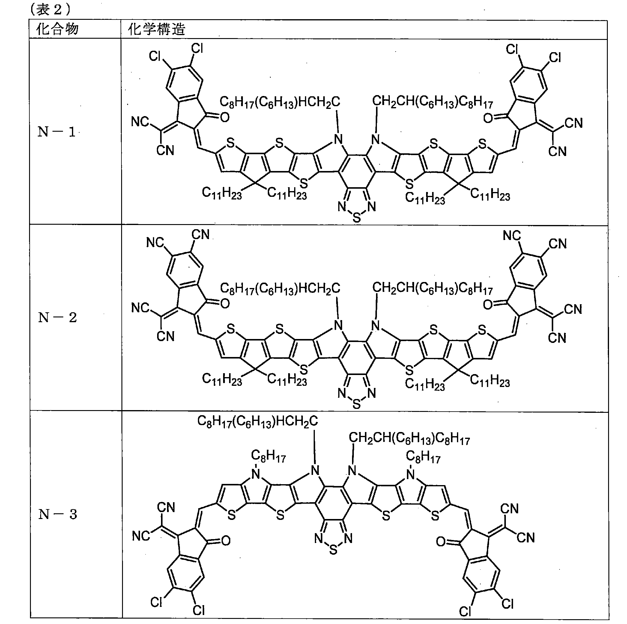

p型半導体材料である高分子化合物P-1は、国際公開第2011/052709号に記載の方法を参考にして合成して使用した。高分子化合物P-2は、国際公開第2013/051676号に記載の方法を参考にして合成して使用した。
n型半導体材料である化合物N-1、N-2、及び化合物N-3は、後述の合成例のとおり合成して使用した。
n型半導体材料である化合物N-4は、Y6(商品名、1-material社製)を市場より入手して使用した。
<合成例1>(化合物2の合成)
下記式に示されるとおり、化合物1を用いて化合物2を合成した。
下記式に示されるとおり、化合物1を用いて化合物2を合成した。
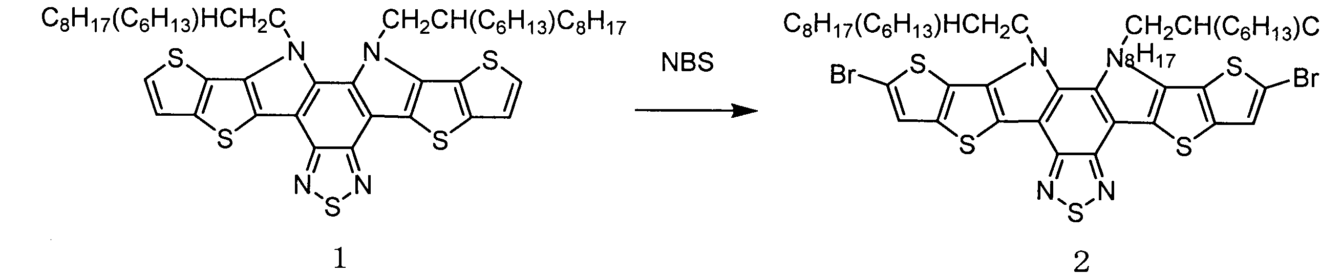
N2ガスで内部の雰囲気を置換した20mL2つ口フラスコにACS Energy Lett.2020,5,3415に記載の方法により合成した化合物1(0.638g、0.072mmol)、テトラヒドロフラン(THF)(4.8mL、0.15M)を仕込み、アイスバスで内温0℃に冷却した。N-ブロモスクシンイミド(NBS)(0.250g、1.40mmol)を加えた後、反応液を常温まで昇温した。
次いで、反応液を30分間撹拌し、反応液に3%Na2SO3水溶液を注いでクエンチし、さらにクロロホルムを加えて有機層を抽出した。得られた有機層を水で1回、塩水(brine)で1回洗浄し、硫酸マグネシウムで脱水し、硫酸マグネシウムをろ過によって除去した後、ろ液をロータリーエバポレーターで全量濃縮して粗生成物を得た。
得られた粗生成物をシリカゲルカラム(展開溶媒:ヘキサン/酢酸エチル=100/0質量%及び96/4質量%)にて精製することにより、目的物を橙色の固体として0.678g(0.649mmol、収率93%)得た。得られた目的物について、NMRスペクトルを解析した。結果は下記のとおりである。
1H-NMR(400MHz, CHLOROFORM-D) δ. 7.42 (s, 2H), 4.61 (d, 2H), 1.94-2.01 (m, 2H), 0.63-1.01 (m, 60H)
1H-NMR(400MHz, CHLOROFORM-D) δ. 7.42 (s, 2H), 4.61 (d, 2H), 1.94-2.01 (m, 2H), 0.63-1.01 (m, 60H)
<合成例2>(化合物3の合成)
下記式に示されるとおり、化合物2を用いて化合物3を合成した。
下記式に示されるとおり、化合物2を用いて化合物3を合成した。
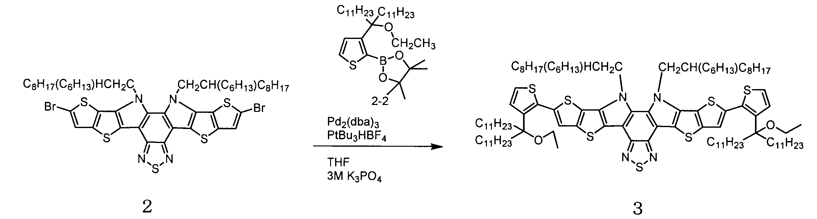
50mL三口フラスコに、化合物2(0.671g、0.64mmol)、国際公開第2012/169605号に記載の方法を参考に合成した上記化合物2-2(0.89g、1.54mmol、)、THF(12.8mL、0.05M)を仕込み、30分間N2ガスで内部の雰囲気を置換した。
次いで、Pd2(dba)3(0.047g、0.05mmol)、P(tBu3)HBF4(0.031g、0.10mmol)、3M K3PO4aq(3.2mL)の順に仕込んだ後に、反応液を60℃に昇温し、2時間撹拌後に、反応液を常温まで冷却した。
次に、反応液から有機層を抽出し、抽出された有機層をトルエンで希釈し、さらに水で2回洗浄した。次いで、硫酸マグネシウムで乾燥し、ろ過した後にロータリーエバポレーターで全量濃縮して粗生成物を得た。
得られた粗生成物をシリカゲルカラム(展開溶媒:ヘキサン/クロロホルム=100/0質量%及び50/50質量%)にて精製することにより、目的物である化合物3を橙色粘性の液体として0.712g(0.399mmol、収率62%)得た。得られた目的物について、NMRスペクトルを解析した。結果は下記のとおりである。
1H-NMR(400MHz, CHLOROFORM-D) δ 7.51 (s, 2H), 7.26 (d, 2H), 7.08 (d, 2H), 4.58 (d, 4H), 3.27 (q, 4H), 2.06-2.12 (m, 2H), 1.84-1.96 (m, 8H), 0.65-1.28 (m, 150H)
1H-NMR(400MHz, CHLOROFORM-D) δ 7.51 (s, 2H), 7.26 (d, 2H), 7.08 (d, 2H), 4.58 (d, 4H), 3.27 (q, 4H), 2.06-2.12 (m, 2H), 1.84-1.96 (m, 8H), 0.65-1.28 (m, 150H)
<実施例1>(化合物4の合成)
下記式に示されるとおり、化合物3を用いて化合物4を合成した。
下記式に示されるとおり、化合物3を用いて化合物4を合成した。
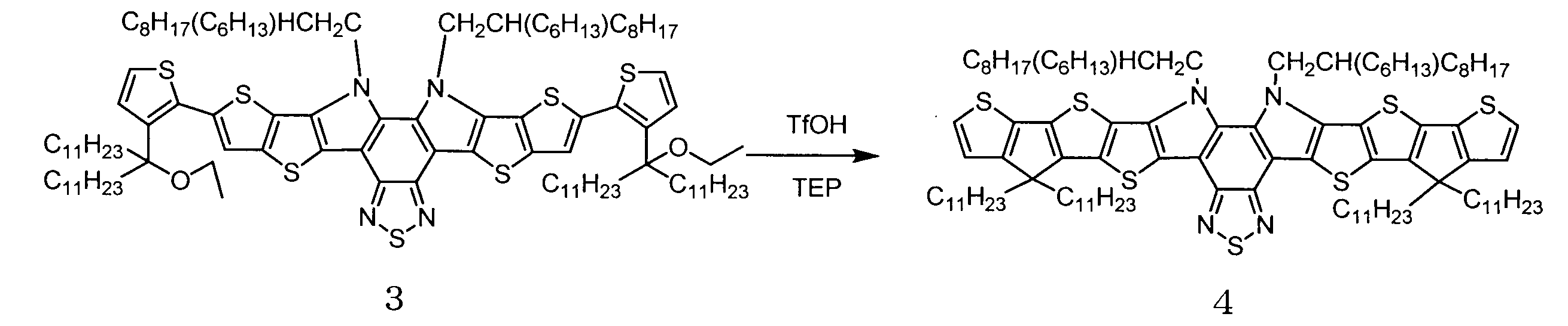
100mL三口フラスコに、化合物3(0.356g、0.20mmol)、脱水トルエン(23.5mL、0.0085M)を仕込み、30分間N2ガスで内部の雰囲気を置換した。氷浴を用いて0℃に冷却した後に、トリフルオロメタンスルホン酸(1.20g、7.90mmol)をさらに三口フラスコ内に仕込み、反応液を常温まで昇温した(工程a)。
反応液を1時間撹拌した後に、水を加えて有機層を抽出し、約3%炭酸水素ナトリウム水で1回、水で2回洗浄した後、硫酸マグネシウムで乾燥し、ろ過した後にロータリーエバポレーターで全量濃縮することにより、濃縮物(濃縮物1)を得た(工程b)。
上記工程(a)及び(b)をもう1回実施して、濃縮物2を得た。得られた濃縮物1及び2を合わせた全濃縮物を用いて下記の操作を実施した。
得られた全濃縮物をシリカゲルカラム(展開溶媒:ヘキサン/クロロホルム=95/5質量%)にて精製することにより、目的物である化合物4を橙色の粘性液体として0.530g(0.313mmol、収率78%)得た。得られた目的物について、NMRスペクトルを解析した。結果は下記のとおりである。
1H-NMR(400MHz, CHLOROFORM-D) δ 7.20 (d, 2H), 7.01 (d, 2H), 4.60 (d, J = 7.8 Hz, 4H), 1.98-2.14 (m, 10H), 0.75-1.27 (m, 138H), 0.62-0.69 (m, 6H)
1H-NMR(400MHz, CHLOROFORM-D) δ 7.20 (d, 2H), 7.01 (d, 2H), 4.60 (d, J = 7.8 Hz, 4H), 1.98-2.14 (m, 10H), 0.75-1.27 (m, 138H), 0.62-0.69 (m, 6H)
<実施例2>(化合物5の合成)
下記式に示されるとおり、化合物4を用いて化合物5を合成した。
下記式に示されるとおり、化合物4を用いて化合物5を合成した。

内部の雰囲気をN2ガスで置換した100mL三口フラスコに、化合物4(0.544g、0.32mmol)、脱水クロロホルム(16mL、0.02M)、Vilsmeier試薬((Chloromethylene)dimethyliminium Chloride)(0.123g、0.96mmol)を仕込み、オイルバスにて内温60℃で2時間保温した。
次いで、三口フラスコをオイルバスから上げて常温まで放冷し、反応液に水を注いでクエンチした後に、飽和炭酸水素ナトリウム水溶液を加えて常温で撹拌した。
反応液から有機層を抽出した後に水で2回洗浄し、硫酸マグネシウムで脱水し、硫酸マグネシウムをろ過によって除去した。得られたろ液をロータリーエバポレーターで全量濃縮して粗生成物を得た。
得られた粗生成物をシリカゲルカラム(展開溶媒:ヘキサン/酢酸エチル=95/5質量%)にて精製することにより、目的物である化合物5を紅色の粘性液体として0.523g(1.32mmol、収率93%)得た。得られた目的物について、NMRスペクトルを解析した。結果は下記のとおりである。
1H-NMR(400MHz, CHLOROFORM-D) δ 9.86 (s, 2H), 7.63 (s, 2H), 4.62 (d, J = 7.8 Hz, 4H), 2.01-2.16 (m, 10H), 0.76-1.30 (m, 138H), 0.62-0.68 (m, 6H)
1H-NMR(400MHz, CHLOROFORM-D) δ 9.86 (s, 2H), 7.63 (s, 2H), 4.62 (d, J = 7.8 Hz, 4H), 2.01-2.16 (m, 10H), 0.76-1.30 (m, 138H), 0.62-0.68 (m, 6H)
<実施例3>(化合物N―1の合成)
下記式に示されるとおり、化合物5を用いて化合物N-1を合成した。
下記式に示されるとおり、化合物5を用いて化合物N-1を合成した。
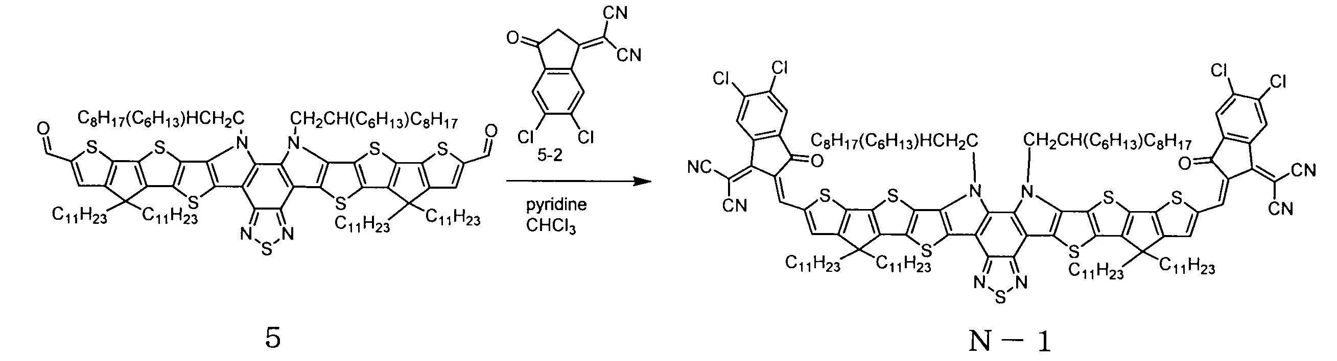
30mLフラスコに、化合物5(0.264g、0.151mmol)、脱水クロロホルム(9g、0.03M)、Adv. Mater. 2017, 29, 1703080.に記載の方法により合成した上記化合物5―2(0.119g、0.452mmol)、pyridine(0.119g、1.51mmol)を仕込み、フラスコを60℃に加熱したオイルバスにつけて保温しつつ3時間撹拌した後、オイルバスからフラスコを上げて常温まで放冷した。
次いで、反応液を水で2回洗浄した後に、桐山漏斗でろ過することで不溶物を除去した。得られたろ液をロータリーエバポレーターで全量濃縮して固体を得た。
得られた固体にクロロホルム22gを加えて60℃にして完溶させた後に、エバポレーターでマス重量4.6gとなるように濃縮し、さらにアセトン21gを加え、析出した固体をろ過して回収することにより、目的物である化合物N-1を黒色固体として0.297g(0.132mmol、収率88%)得た。得られた目的物について、NMRスペクトルを解析した。結果は下記のとおりである。
1H-NMR(400MHz, CHLOROFORM-D) δ 8.94 (s, 2H), 8.75 (s, 2H), 7.90 (s, 2H), 7.67 (s, 1H), 4.65 (d, 4H), 2.06-2.18 (m, 10H), 0.73-1.30 (m, 138H), 0.66-0.71 (m, 6H)
1H-NMR(400MHz, CHLOROFORM-D) δ 8.94 (s, 2H), 8.75 (s, 2H), 7.90 (s, 2H), 7.67 (s, 1H), 4.65 (d, 4H), 2.06-2.18 (m, 10H), 0.73-1.30 (m, 138H), 0.66-0.71 (m, 6H)
<実施例4>(化合物N―2の合成)
下記式に示されるとおり、化合物5を用いて化合物N-2を合成した。
下記式に示されるとおり、化合物5を用いて化合物N-2を合成した。
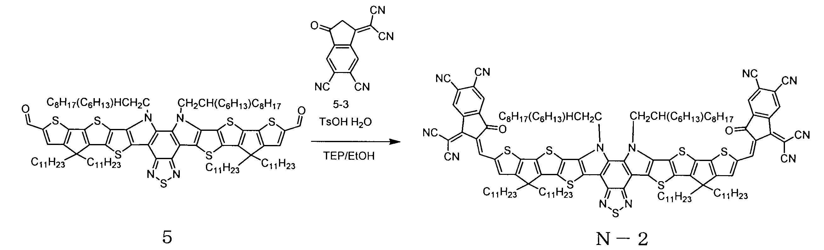
30mLフラスコに化合物5(0.295g、0.169mmol)、国際公開第2020/109823号に記載の方法に従って合成した上記化合物5-3(0.124g、0.506mmol)、pTsOH・H2O(0.096g、0.506mmol)、EtOH(3mL)、トルエン(6mL)、MgSO4(0.15g)を仕込み、60℃に昇温したオイルバスにつけて保温した。4時間撹拌後にオイルバスからフラスコを上げて常温まで放冷し、水を10g加えエバポレーターでEtOHとトルエンを除去した後に、析出した固体をろ過し、アセトンで洗浄することにより粗生成物を得た。
得られた粗生成物をリサイクル分取GPC(展開溶媒:クロロホルム)を用いて精製し、回収されたフラクションをエバポレーターで濃縮した。
濃縮された粗生成物をシリカゲルカラム(展開溶媒:ヘキサン/クロロホルム=20/80質量%)にてさらに精製することにより、化合物N-2を黒色固体として0.276g(0.124mmol、収率74%)得た。得られた目的物について、NMRスペクトルを解析した。結果は下記のとおりである。
1H-NMR(400MHz, CHLOROFORM-D) δ 9.00 (4H), 8.15 (2H), 7.64 (2H), 4.66 (d, J = 7.3 Hz, 4H), 2.09-2.21 (m, 10H), 0.75-1.33 (m, 138H), 0.64-0.73 (m, 6H)
1H-NMR(400MHz, CHLOROFORM-D) δ 9.00 (4H), 8.15 (2H), 7.64 (2H), 4.66 (d, J = 7.3 Hz, 4H), 2.09-2.21 (m, 10H), 0.75-1.33 (m, 138H), 0.64-0.73 (m, 6H)
<合成例5>(化合物7の合成)
下記式に示されるとおり、化合物6を用いて化合物7を合成した。
下記式に示されるとおり、化合物6を用いて化合物7を合成した。

内部の雰囲気をN2ガスで置換した50mL四口フラスコに、上記式で表される化合物6(1.17g、4.01mmol、東京化成社製)を脱水THF(0.28M)に溶解させ、酸素濃度が0.02%を下回っていることを確認した後にドライアイス/アセトンバスに四口フラスコを浸して内温が-60℃以下になるまで冷却した。
次いで、1.56MのnBuLiヘキサン溶液(2.57mL、1.0eq、4.01mmol)を、内温が-60℃を超えないようにゆっくりと滴下した。1時間保温した後に、0℃まで昇温し30分間保温した後に、-60℃以下となるように再度冷却した。
次に、ClSn(Bu)3(1.03eq、7.97g)を内温が0℃を超えないようにゆっくりと滴下した。2時間保温した後に四口フラスコをバスから上げ、常温まで昇温させた。さらにヘキサン3gと水0.1gを加え、30分間攪拌した後に、硫酸ナトリウムで脱水し、硫酸ナトリウムをろ過によって除去した。
得られたろ液をロータリーエバポレーターで全量濃縮して目的物である化合物7の粗生成物を黒緑色のオイルとして2.43g得た(見かけ収率104%)。
<合成例6>(化合物8の合成)
下記式に示されるとおり、化合物7及び化合物7-2を用いて化合物8を合成した。
下記式に示されるとおり、化合物7及び化合物7-2を用いて化合物8を合成した。

50mL三口フラスコに、上記合成例5で得られた化合物7(2.33g)、化合物7-2(0.82g、2.14mmol、Angene International社製)、脱水トルエン(28mL、0.15M)を仕込み、30分間N2ガスで内部の雰囲気を置換した。Pd2(dba)3(0.16g、0.17mmol)、P(o-tolyl)3(0.10g、0.34mmol)の順に仕込んだ後に80℃に昇温した。2時間撹拌後に、常温まで冷却し、ロータリーエバポレーターで全量濃縮した。
次いで、アセトンでリパルプ洗浄することでアセトンリパルプ品を得た。アセトンリパルプ洗浄により得られたろ液を全量濃縮し、ヘキサンでリパルプすることでヘキサンリパルプ品を得た。
得られたアセトンリパルプ品とヘキサンリパルプ品とを合わせてクロロホルム/アセトンの混合溶液でリパルプ洗浄した後、ろ過、乾燥することで目的物である化合物8を紫黒色の固体として1.34g(1.73mmol、収率78%)得た。
<実施例5>(化合物10の合成)
下記式に示されるとおり、化合物8を用いて化合物10を合成した。
下記式に示されるとおり、化合物8を用いて化合物10を合成した。

100mLフラスコに、化合物8(1.19g、1.48mmol)、PPh3(3.88g、14.8mmol)、ODCB(30mL、0.05M)を仕込み、30分間N2ガスで内部の雰囲気を置換した後に180℃に昇温した。7時間撹拌後に、常温まで冷却し、ロータリーエバポレーターで全量濃縮することで、化合物9の粗生成物を6.12g(見かけ収率559%)得た。300mL三口フラスコに、得られた粗生成物0.110g、KI(0.074g、0.04mmol)、K2CO3(1.22g、8.86mmol)、9-(Bromomethyl)nonadecane(4.27g、11.8mmol)、脱水DMF(21mL、0.07M)を仕込み、30分間N2ガスで内部の雰囲気を置換した後に90℃に昇温した。次いで6時間保温した後に常温まで冷却した。
次に、三口フラスコにクロロホルムを加え、水で3回分液洗浄した後に、硫酸マグネシウムで脱水し、硫酸マグネシウムをろ過によって除去した。得られたろ液をロータリーエバポレーターで濃縮して粗生成物を得た。
得られた粗生成物をシリカゲルカラム(展開溶媒はキサン/クロロホルム=50/50質量%~40/60質量%とした。)にて精製することにより、化合物10を赤色の粘性液体として0.157g得た(収率8%)。
得られた目的物について、NMRスペクトルを解析した。結果は下記のとおりである。
1H-NMR(400MHz, CHLOROFORM-D) δ 7.16 (d, J = 5.0 Hz, 2H), 7.06 (d, J = 5.0 Hz, 2H), 4.64-4.70 (m, 2H), 4.39-4.54 (m, 6H), 1.99-2.06 (m, 6H), 0.25-1.34 (m, 106H)
1H-NMR(400MHz, CHLOROFORM-D) δ 7.16 (d, J = 5.0 Hz, 2H), 7.06 (d, J = 5.0 Hz, 2H), 4.64-4.70 (m, 2H), 4.39-4.54 (m, 6H), 1.99-2.06 (m, 6H), 0.25-1.34 (m, 106H)
<実施例6>(化合物11の合成)
下記式に示されるとおり、化合物10を用いて化合物11を合成した。
下記式に示されるとおり、化合物10を用いて化合物11を合成した。

N2ガスで内部の雰囲気を置換した20mLフラスコに、化合物10であるNFA-177c(0.116g、0.09mmol)、脱水クロロホルム(3.6mL、0.03M)、Vilsmeier試薬((Chloromethylene)dimethyliminium Chloride)(0.034g、0.27mmol)を仕込み、オイルバスにて内温60℃で3時間保温した。
次いで、フラスコをオイルバスから上げて常温まで放冷し、反応液に水を注いでクエンチした後に、飽和炭酸水素ナトリウム水溶液を加えて常温で撹拌した。
次に、反応液から有機層を抽出した後に、有機層を水で2回洗浄した後、硫酸マグネシウムで脱水し、硫酸マグネシウムをろ過によって除去して粗生成物を得た。
次いで、粗生成物をシリカゲルカラム(展開溶媒:ヘキサン/酢酸エチル/クロロホルム=75/15/10質量%)にてさらに精製することにより、化合物11である目的物を橙色の固体として0.0827g(0.0609mmol、収率69%)得た。得られた目的物について、NMRスペクトルを解析した。結果は下記のとおりである。
1H-NMR(400MHz, CHLOROFORM-D) δ9.87 (2H), 7.69 (2H), 4.62-4.68 (m, 2H), 4.42-4.53 (m, 6H), 1.99-2.02 (m, 6H), 0.31-1.49 (m, 106H)
1H-NMR(400MHz, CHLOROFORM-D) δ9.87 (2H), 7.69 (2H), 4.62-4.68 (m, 2H), 4.42-4.53 (m, 6H), 1.99-2.02 (m, 6H), 0.31-1.49 (m, 106H)
<実施例7>(化合物N-3の合成)
下記式に示されるとおり、化合物11を用いて化合物N-3を合成した。
下記式に示されるとおり、化合物11を用いて化合物N-3を合成した。

50mLフラスコに、化合物11(0.083g、0.066mmol)、脱水クロロホルム(3.96g、0.03M)、化合物5-2(0.058g、0.73mmol)、pyridine(0.058g、0.73mmol)を仕込み、60℃に加熱したオイルバスにつけて保温した。2時間撹拌後にフラスコをオイルバスから上げて常温まで放冷した。
次いで、反応液を水で2回洗浄した後に、全濃縮し、アセトンを加えてスラリー洗浄をすることで粗生成物を得た。
次に、粗生成物をシリカゲルカラム(展開溶媒:クロロホルム=100質量%)にてさらに精製した後、アセトンでリパルプ洗浄することで、目的物である化合物N-3を紫黒色の固体として0.11g(0.061mmol、収率100%)得た。
<実施例8>(インクI-1の調製)
溶媒であるo-キシレン(oXAP)と安息香酸メチル(MBZ)(95/5=体積%)の混合溶液に、p型半導体材料である高分子化合物P―1をインクの全重量に対し1.3質量%の濃度となるように、また、n型半導体材料である化合物N-1をインクの全重量に対して1.3質量%の濃度となるように(p型半導体材料/n型半導体材料=1/1)混合し、60℃で8時間撹拌を行って得られた混合液をフィルターを用いてろ過することにより、インク(I-1)を得た。
溶媒であるo-キシレン(oXAP)と安息香酸メチル(MBZ)(95/5=体積%)の混合溶液に、p型半導体材料である高分子化合物P―1をインクの全重量に対し1.3質量%の濃度となるように、また、n型半導体材料である化合物N-1をインクの全重量に対して1.3質量%の濃度となるように(p型半導体材料/n型半導体材料=1/1)混合し、60℃で8時間撹拌を行って得られた混合液をフィルターを用いてろ過することにより、インク(I-1)を得た。
<実施例9>(インクI-2の調製)
n型半導体材料として下記表4に示す化合物を使用した以外は、実施例8と同様にして、インク(I-2)の調製を行った。
n型半導体材料として下記表4に示す化合物を使用した以外は、実施例8と同様にして、インク(I-2)の調製を行った。
<実施例10>(インク(I-3)の調製)
n型半導体材料として下記表4に示す化合物を使用した以外は、実施例8と同様にして、インク(I-3)の調製を行った。
n型半導体材料として下記表4に示す化合物を使用した以外は、実施例8と同様にして、インク(I-3)の調製を行った。
<実施例11>(インクI-4の調製)
溶媒をオルトジクロロベンゼン(ODCB)とし、n型半導体材料として下記表4に示す化合物を使用した以外は、実施例8と同様にして、インク(I-4)の調製を行った。
溶媒をオルトジクロロベンゼン(ODCB)とし、n型半導体材料として下記表4に示す化合物を使用した以外は、実施例8と同様にして、インク(I-4)の調製を行った。
<実施例12>(インク(I-5)の調製)
溶媒をオルトジクロロベンゼンとし、n型半導体材料として下記表4に示す化合物を使用した以外は、実施例8と同様にして、インク(I-5)の調製を行った。
溶媒をオルトジクロロベンゼンとし、n型半導体材料として下記表4に示す化合物を使用した以外は、実施例8と同様にして、インク(I-5)の調製を行った。
<比較例1>(インク(I-6)の調製)
溶媒をオルトジクロロベンゼンとし、n型半導体材料として下記表4に示す化合物を使用した以外は、実施例8と同様にして、インク(I-6)の調製を行った。
溶媒をオルトジクロロベンゼンとし、n型半導体材料として下記表4に示す化合物を使用した以外は、実施例8と同様にして、インク(I-6)の調製を行った。
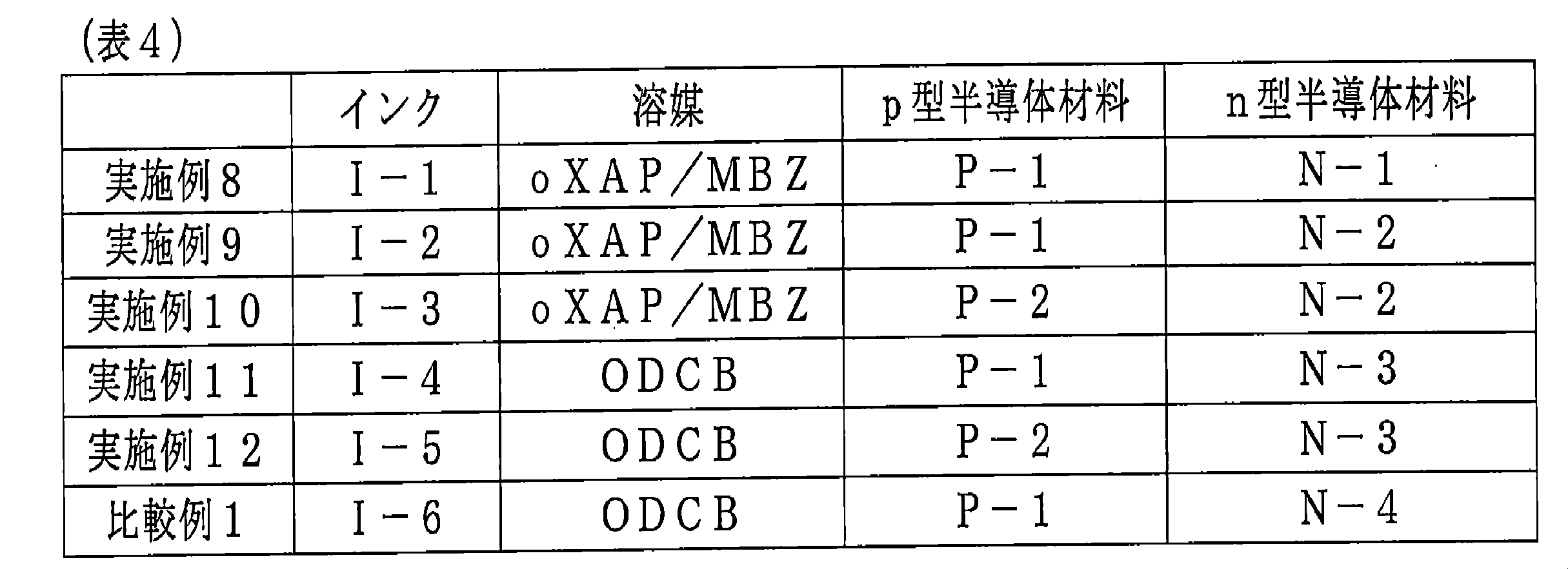
<実施例13>(光電変換素子の製造及び評価)
(1)光電変換素子及びその封止体の製造
スパッタ法により50nmの厚さでITOの薄膜(陽極)が形成されたガラス基板を用意し、このガラス基板に対し、表面処理としてオゾンUV処理を行った。
(1)光電変換素子及びその封止体の製造
スパッタ法により50nmの厚さでITOの薄膜(陽極)が形成されたガラス基板を用意し、このガラス基板に対し、表面処理としてオゾンUV処理を行った。
次に、インク(I-1)を、ITOの薄膜上にスピンコート法により塗布して塗膜を形成した後、窒素ガス雰囲気下で100℃に加熱したホットプレートを用いて10分間加熱処理して乾燥させ、活性層を形成した(プリベーク工程)。形成された活性層の厚さは約300nmであった。
次に、形成された活性層上にスピンコート法によりZnO(テイカ社製、製品名:HTD-711Z)を塗布して約50nmの厚さの電子輸送層を形成した。
次いで、形成された電子輸送層上に、銀(Ag)層を約60nmの厚さで形成し、陰極とした。
以上の工程により光電変換素子が、ガラス基板上に製造された。
以上の工程により光電変換素子が、ガラス基板上に製造された。
次に、製造された光電変換素子の周辺を囲むように、支持基板であるガラス基板上に封止材であるUV硬化性封止剤を塗布し、封止基板であるガラス基板を貼り合わせた後、UV光を照射することで、光検出素子を支持基板と封止基板との間隙に封止することにより光電変換素子の封止体を得た。支持基板と封止基板との間隙に封止された光電変換素子の厚さ方向から見たときの平面的な形状は2mm×2mmの正方形であった。得られた封止体をサンプル1とした。
(2)光電変換素子の評価(暗電流)
製造されたサンプル1に対し、光が照射されない暗状態において、光検出素子の封止体に-10Vから2Vの電圧を印加し、公知の手法を用いて測定された-4Vの逆バイアス電圧印加時の電流値を暗電流の値として得た。結果を下記表5に示す。
製造されたサンプル1に対し、光が照射されない暗状態において、光検出素子の封止体に-10Vから2Vの電圧を印加し、公知の手法を用いて測定された-4Vの逆バイアス電圧印加時の電流値を暗電流の値として得た。結果を下記表5に示す。
<実施例14から17及び比較例2>(光電変換素子の製造及び評価)
インク(I-1)の代わりに、インク(I-2)~(I-6)を用い、既に説明した実施例13と同様にして、光電変換素子の封止体を製造し、評価した。結果を下記表5に示す。
インク(I-1)の代わりに、インク(I-2)~(I-6)を用い、既に説明した実施例13と同様にして、光電変換素子の封止体を製造し、評価した。結果を下記表5に示す。
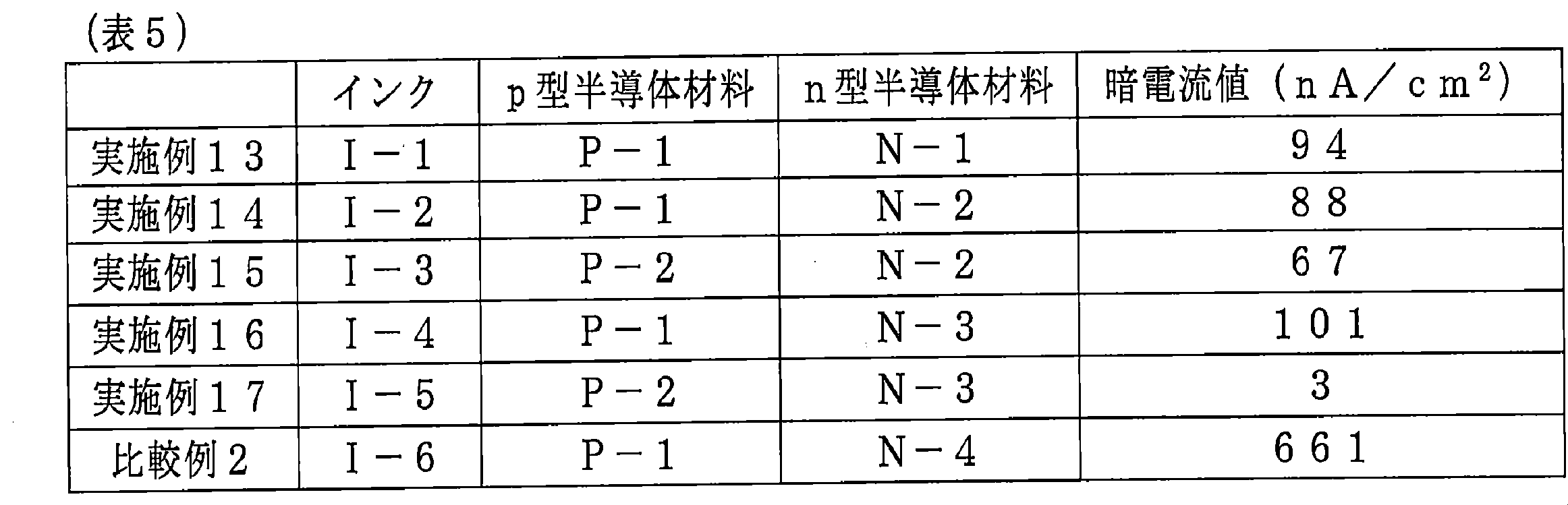
表5に示されるとおり、本発明の化合物をn型半導体材料として用いた光電変換素子によれば、従来のn型半導体材料を用いた光電変換素子と比較して、暗電流(値)を1/200~1/6程度にまで低減することができることがわかった。
1 イメージ検出部
2 表示装置
10 光電変換素子
11、210 支持基板
12 陽極
13 正孔輸送層
14 活性層
15 電子輸送層
16 陰極
17 封止部材
20 CMOSトランジスタ基板
30 層間絶縁膜
32 層間配線部
40 封止層
42 シンチレータ
44 反射層
46 保護層
50 カラーフィルター
100 指紋検出部
200 表示パネル部
200a 表示領域
220 有機EL素子
230 タッチセンサーパネル
240 封止基板
300 静脈検出部
302 ガラス基板
304 光源部
306 カバー部
310 挿入部
400 TOF型測距装置用イメージ検出部
401 絶縁層
402 浮遊拡散層
404 フォトゲート
406 遮光部
Claims (12)
- 下記式(I)で表される化合物。
A1―P―A2 (I)
(式(I)中、
A1及びA2は、それぞれ独立して、電子求引性の1価の基であり、
Pは、下記式(1)で表される2価の基である。)

Xは、-S-で表される基、-O-で表される基、-Se-で表される基、又は-NR-で表される基を表し、
Y1及びY2は、それぞれ独立して、-S-で表される基、-CR1R2-で表される基、-SiR1R2-で表される基、-NR-で表される基、-C(=O)-で表される基、-C(=O)-NR-で表される基、-NR-C(=O)-で表される基、-CR1R2-O-で表される基、-O-CR1R2-で表される基、-C(=O)-CR1R2-で表される基、又は-CR1R2-C(=O)-で表される基を表し、
Ar1及びAr2は、それぞれ独立して、置換基を有していてもよく複数の環構造がさらに縮環していてもよい芳香族炭素環又は置換基を有していてもよく複数の環構造がさらに縮環していてもよい芳香族複素環を表し、
Ar3及びAr4は、それぞれ独立して、置換基を有していてもよく複数の環構造がさらに縮環していてもよい2価の芳香族炭素環基又は置換基を有していてもよく複数の環構造が縮環していてもよい2価の芳香族複素環基を表し、
n及びmは、それぞれ独立して、0、1、2又は3を表し、
R、R1及びR2は、それぞれ独立して、
水素原子、
ハロゲン原子、
置換基を有していてもよいアルキル基、
置換基を有していてもよいシクロアルキル基、
置換基を有していてもよいアリール基、
置換基を有していてもよいアルキルオキシ基、
置換基を有していてもよいシクロアルキルオキシ基、
置換基を有していてもよいアリールオキシ基、
置換基を有していてもよいアルキルチオ基、
置換基を有していてもよいシクロアルキルチオ基、
置換基を有していてもよいアリールチオ基、
置換基を有していてもよい1価の複素環基、
置換基を有していてもよい置換アミノ基、
置換基を有していてもよいアシル基、
置換基を有していてもよいイミン残基、
置換基を有していてもよいアミド基、
置換基を有していてもよい酸イミド基、
置換基を有していてもよい置換オキシカルボニル基、
置換基を有していてもよいアルケニル基、
置換基を有していてもよいシクロアルケニル基、
置換基を有していてもよいアルキニル基、
置換基を有していてもよいシクロアルキニル基、
シアノ基、
ニトロ基、
-C(=O)-Raで表される基、又は
-SO2-Rbで表される基を表し、
Ra及びRbは、それぞれ独立して、
水素原子、
置換基を有していてもよいアルキル基、
置換基を有していてもよいアリール基、
置換基を有していてもよいアルキルオキシ基、
置換基を有していてもよいアリールオキシ基、又は
置換基を有していてもよい1価の複素環基を表し、
複数あるR、R1及びR2は、同一であっても異なっていてもよい。) - Y1及びY2が-NR-で表される基であるか、又はPが下記式(2)で表される2価の基である、請求項1に記載の化合物。

Y3及びY4は、それぞれ独立して、-S-で表される基、-CR1R2-で表される基、-SiR1R2-で表される基、-NR-で表される基、-C(=O)-で表される基、-C(=O)-NR-で表される基、-CR1R2-O-で表される基、-O-CR1R2-で表される基、-C(=O)-CR1R2-で表される基、又は-CR1R2-C(=O)-で表される基を表し、
X、R、R1及びR2は、前記定義のとおりである。) - Xが、-S-で表される基、又は-O-で表される基である、請求項1又は2に記載の化合物。
- Ar3及びAr4が、それぞれ独立して、チオフェン環を含み、置換基を有していてもよく複数の環構造が縮環していてもよい2価の芳香族複素環基である、請求項1又は2に記載の化合物。
- A1及びA2が、それぞれ独立して、シアノ基、カルボニル基及びチオカルボニル基からなる群から選択される1種以上を含む電子求引性の基である、請求項1又は2に記載の化合物。
- p型半導体材料と、n型半導体材料とを含み、該n型半導体材料として、請求項1又は2に記載の化合物を含む、組成物。
- 請求項6に記載の組成物と、溶媒とを含むインク。
- 陽極と、陰極と、該陽極と該陰極との間に設けられており、p型半導体材料及びn型半導体材料を含む活性層とを含み、該n型半導体材料として、請求項1又は2に記載の化合物を含む、光電変換素子。
- 光検出素子である、請求項8に記載の光電変換素子。
- 請求項9に記載の光電変換素子を含む、イメージセンサー。
- 下記式(3)で表される化合物。

Xは、-S-で表される基、-O-で表される基、-Se-で表される基、又は-N(R)-で表される基を表し、
Y1及びY2は、それぞれ独立して、-S-で表される基、-CR1R2-で表される基、-SiR1R2-で表される基、-NR-で表される基、-C(=O)-で表される基、-C(=O)-NR-で表される基、-NR-C(=O)-で表される基、-CR1R2-O-で表される基、-O-CR1R2-で表される基、-C(=O)-CR1R2-で表される基、又は-CR1R2-C(=O)-で表される基を表し、
Ar1及びAr2は、それぞれ独立して、置換基を有していてもよく複数の環構造がさらに縮環していてもよい芳香族炭素環又は置換基を有していてもよく複数の環構造がさらに縮環していてもよい芳香族複素環を表し、
R、R1及びR2は、それぞれ独立して、
水素原子、
ハロゲン原子、
置換基を有していてもよいアルキル基、
置換基を有していてもよいシクロアルキル基、
置換基を有していてもよいアリール基、
置換基を有していてもよいアルキルオキシ基、
置換基を有していてもよいシクロアルキルオキシ基、
置換基を有していてもよいアリールオキシ基、
置換基を有していてもよいアルキルチオ基、
置換基を有していてもよいシクロアルキルチオ基、
置換基を有していてもよいアリールチオ基、
置換基を有していてもよい1価の複素環基、
置換基を有していてもよい置換アミノ基、
置換基を有していてもよいアシル基、
置換基を有していてもよいイミン残基、
置換基を有していてもよいアミド基、
置換基を有していてもよい酸イミド基、
置換基を有していてもよい置換オキシカルボニル基、
置換基を有していてもよいアルケニル基、
置換基を有していてもよいシクロアルケニル基、
置換基を有していてもよいアルキニル基、
置換基を有していてもよいシクロアルキニル基、
シアノ基、
ニトロ基、
-C(=O)-Raで表される基、又は
-SO2-Rbで表される基を表し、
Ra及びRbは、それぞれ独立して、
水素原子、
置換基を有していてもよいアルキル基、
置換基を有していてもよいアリール基、
置換基を有していてもよいアルキルオキシ基、
置換基を有していてもよいアリールオキシ基、又は
置換基を有していてもよい1価の複素環基を表し、
複数あるR、R1及びR2は、同一であっても異なっていてもよい。) - Y1及びY2が-NR-で表される基であるか、又は下記式(4)で表される化合物である、請求項11に記載の化合物。

Y3及びY4は、それぞれ独立して、-S-で表される基、-CR1R2-で表される基、-SiR1R2-で表される基、-NR-で表される基、-C(=O)-で表される基、-C(=O)-NR-で表される基、-CR1R2-O-で表される基、-O-CR1R2-で表される基、-C(=O)-CR1R2-で表される基、又は-CR1R2-C(=O)-を表し、
X、R、R1及びR2は、前記定義のとおりである。
Wは、水素原子、ハロゲン原子、ホウ酸エステル残基、ジヒドロキシボリル基、ホルミル基、ビニル基又は置換スタンニル基を表す。2個あるWは、同一であっても異なっていてもよい。)
Applications Claiming Priority (2)
| Application Number | Priority Date | Filing Date | Title |
|---|---|---|---|
| JP2021-205799 | 2021-12-20 | ||
| JP2021205799 | 2021-12-20 |
Publications (1)
| Publication Number | Publication Date |
|---|---|
| WO2023120359A1 true WO2023120359A1 (ja) | 2023-06-29 |
Family
ID=86902558
Family Applications (1)
| Application Number | Title | Priority Date | Filing Date |
|---|---|---|---|
| PCT/JP2022/046175 Ceased WO2023120359A1 (ja) | 2021-12-20 | 2022-12-15 | 化合物及びこれを用いた光電変換素子 |
Country Status (3)
| Country | Link |
|---|---|
| JP (1) | JP2023091753A (ja) |
| TW (1) | TW202330555A (ja) |
| WO (1) | WO2023120359A1 (ja) |
Citations (5)
| Publication number | Priority date | Publication date | Assignee | Title |
|---|---|---|---|---|
| WO2020052194A1 (zh) * | 2018-09-10 | 2020-03-19 | 中南大学 | 一种稠环苯并噻二唑基非富勒烯受体材料及其制备方法和应用 |
| CN111285885A (zh) * | 2020-03-17 | 2020-06-16 | 香港科技大学深圳研究院 | 稠环苯并硒二唑非富勒烯受体材料及其制备方法和应用 |
| JP2021113184A (ja) * | 2020-01-17 | 2021-08-05 | レイナジー テック インコーポレイション | ベンゾセレナジアゾールを含有する非フラーレン系アクセプター化合物、及びそれを含む有機光電素子 |
| CN113583019A (zh) * | 2021-08-03 | 2021-11-02 | 中国科学院长春应用化学研究所 | Ada’da型全稠环小分子及其制备方法与应用 |
| US20220376181A1 (en) * | 2021-04-29 | 2022-11-24 | Raynergy Tek Incorporation | Organic semiconductor device |
-
2022
- 2022-12-09 JP JP2022197057A patent/JP2023091753A/ja active Pending
- 2022-12-15 WO PCT/JP2022/046175 patent/WO2023120359A1/ja not_active Ceased
- 2022-12-16 TW TW111148577A patent/TW202330555A/zh unknown
Patent Citations (5)
| Publication number | Priority date | Publication date | Assignee | Title |
|---|---|---|---|---|
| WO2020052194A1 (zh) * | 2018-09-10 | 2020-03-19 | 中南大学 | 一种稠环苯并噻二唑基非富勒烯受体材料及其制备方法和应用 |
| JP2021113184A (ja) * | 2020-01-17 | 2021-08-05 | レイナジー テック インコーポレイション | ベンゾセレナジアゾールを含有する非フラーレン系アクセプター化合物、及びそれを含む有機光電素子 |
| CN111285885A (zh) * | 2020-03-17 | 2020-06-16 | 香港科技大学深圳研究院 | 稠环苯并硒二唑非富勒烯受体材料及其制备方法和应用 |
| US20220376181A1 (en) * | 2021-04-29 | 2022-11-24 | Raynergy Tek Incorporation | Organic semiconductor device |
| CN113583019A (zh) * | 2021-08-03 | 2021-11-02 | 中国科学院长春应用化学研究所 | Ada’da型全稠环小分子及其制备方法与应用 |
Also Published As
| Publication number | Publication date |
|---|---|
| JP2023091753A (ja) | 2023-06-30 |
| TW202330555A (zh) | 2023-08-01 |
Similar Documents
| Publication | Publication Date | Title |
|---|---|---|
| JP7791662B2 (ja) | 化合物及びこれを用いた光電変換素子 | |
| JP7284128B2 (ja) | 光電変換素子及びその製造方法 | |
| JP6927887B2 (ja) | 高分子化合物およびそれを用いた有機光電変換素子 | |
| WO2020071223A1 (ja) | 光電変換素子及びその製造方法 | |
| WO2024172105A1 (ja) | 化合物、組成物、インク、光電変換素子、光センサー、及び光電変換材料 | |
| US20230363184A1 (en) | Photoelectric conversion element and method for manufacturing same | |
| WO2023008376A1 (ja) | 化合物、組成物及び光電変換素子 | |
| KR102545540B1 (ko) | 잉크 조성물의 제조 방법 | |
| US20240023422A1 (en) | Composition, film, organic photoelectric conversion element, and photodetection element | |
| WO2022224893A1 (ja) | インク組成物及びその製造方法 | |
| WO2021065374A1 (ja) | 光電変換素子 | |
| JP2023020911A (ja) | 化合物、組成物及び光電変換素子 | |
| JP2023057054A (ja) | 組成物及びインク組成物 | |
| JP2023091753A (ja) | 化合物及びこれを用いた光電変換素子 | |
| WO2023100844A1 (ja) | 化合物及びこれを用いた光電変換素子 | |
| JP2023057055A (ja) | 組成物及びインク組成物 | |
| JP2025077474A (ja) | 化合物、組成物、インク、光電変換素子、及び光センサー | |
| JP2025097891A (ja) | 化合物、組成物、インク、光電変換素子、及び光センサー | |
| CN117769897A (zh) | 化合物、组合物和光电转换元件 | |
| WO2025134981A1 (ja) | 化合物、組成物、インク、光電変換素子、及び光センサー | |
| WO2025211175A1 (ja) | 組成物、光電変換素子、及び光センサー |
Legal Events
| Date | Code | Title | Description |
|---|---|---|---|
| 121 | Ep: the epo has been informed by wipo that ep was designated in this application |
Ref document number: 22911067 Country of ref document: EP Kind code of ref document: A1 |
|
| NENP | Non-entry into the national phase |
Ref country code: DE |
|
| 122 | Ep: pct application non-entry in european phase |
Ref document number: 22911067 Country of ref document: EP Kind code of ref document: A1 |