WO2023116201A1 - Micro-lens based on high-refractive-index dielectric substrate - Google Patents
Micro-lens based on high-refractive-index dielectric substrate Download PDFInfo
- Publication number
- WO2023116201A1 WO2023116201A1 PCT/CN2022/128464 CN2022128464W WO2023116201A1 WO 2023116201 A1 WO2023116201 A1 WO 2023116201A1 CN 2022128464 W CN2022128464 W CN 2022128464W WO 2023116201 A1 WO2023116201 A1 WO 2023116201A1
- Authority
- WO
- WIPO (PCT)
- Prior art keywords
- dielectric substrate
- refractive index
- air cavity
- concave air
- high refractive
- Prior art date
Links
- 239000000758 substrate Substances 0.000 title claims abstract description 73
- 238000003384 imaging method Methods 0.000 claims description 14
- 229910052710 silicon Inorganic materials 0.000 claims description 13
- 239000010703 silicon Substances 0.000 claims description 13
- 229910052732 germanium Inorganic materials 0.000 claims description 3
- GNPVGFCGXDBREM-UHFFFAOYSA-N germanium atom Chemical compound [Ge] GNPVGFCGXDBREM-UHFFFAOYSA-N 0.000 claims description 3
- XUIMIQQOPSSXEZ-UHFFFAOYSA-N Silicon Chemical compound [Si] XUIMIQQOPSSXEZ-UHFFFAOYSA-N 0.000 description 12
- 229910000661 Mercury cadmium telluride Inorganic materials 0.000 description 10
- 238000010586 diagram Methods 0.000 description 9
- MCMSPRNYOJJPIZ-UHFFFAOYSA-N cadmium;mercury;tellurium Chemical compound [Cd]=[Te]=[Hg] MCMSPRNYOJJPIZ-UHFFFAOYSA-N 0.000 description 8
- 239000000463 material Substances 0.000 description 6
- 230000005684 electric field Effects 0.000 description 4
- 238000012634 optical imaging Methods 0.000 description 4
- 238000001514 detection method Methods 0.000 description 3
- 230000009286 beneficial effect Effects 0.000 description 2
- 230000000694 effects Effects 0.000 description 2
- 238000009434 installation Methods 0.000 description 2
- 238000000034 method Methods 0.000 description 2
- 239000000203 mixture Substances 0.000 description 2
- 238000013041 optical simulation Methods 0.000 description 2
- 230000005540 biological transmission Effects 0.000 description 1
- 238000004364 calculation method Methods 0.000 description 1
- 238000000576 coating method Methods 0.000 description 1
- 239000006185 dispersion Substances 0.000 description 1
- 238000001459 lithography Methods 0.000 description 1
- 238000004519 manufacturing process Methods 0.000 description 1
- 238000012986 modification Methods 0.000 description 1
- 230000004048 modification Effects 0.000 description 1
- 230000003287 optical effect Effects 0.000 description 1
- 238000004088 simulation Methods 0.000 description 1
- 230000004304 visual acuity Effects 0.000 description 1
Classifications
-
- G—PHYSICS
- G02—OPTICS
- G02B—OPTICAL ELEMENTS, SYSTEMS OR APPARATUS
- G02B3/00—Simple or compound lenses
-
- G—PHYSICS
- G02—OPTICS
- G02B—OPTICAL ELEMENTS, SYSTEMS OR APPARATUS
- G02B3/00—Simple or compound lenses
- G02B3/12—Fluid-filled or evacuated lenses
-
- G—PHYSICS
- G02—OPTICS
- G02B—OPTICAL ELEMENTS, SYSTEMS OR APPARATUS
- G02B1/00—Optical elements characterised by the material of which they are made; Optical coatings for optical elements
- G02B1/10—Optical coatings produced by application to, or surface treatment of, optical elements
- G02B1/11—Anti-reflection coatings
-
- H—ELECTRICITY
- H01—ELECTRIC ELEMENTS
- H01L—SEMICONDUCTOR DEVICES NOT COVERED BY CLASS H10
- H01L27/00—Devices consisting of a plurality of semiconductor or other solid-state components formed in or on a common substrate
- H01L27/14—Devices consisting of a plurality of semiconductor or other solid-state components formed in or on a common substrate including semiconductor components sensitive to infrared radiation, light, electromagnetic radiation of shorter wavelength or corpuscular radiation and specially adapted either for the conversion of the energy of such radiation into electrical energy or for the control of electrical energy by such radiation
- H01L27/144—Devices controlled by radiation
- H01L27/146—Imager structures
- H01L27/14601—Structural or functional details thereof
- H01L27/14625—Optical elements or arrangements associated with the device
- H01L27/14627—Microlenses
Definitions
- the invention relates to the technical field of micro-nano optics and optical imaging, in particular to a microlens based on a high-refractive-index medium substrate.
- the finite aperture size of the lens will diffract the incident light, which makes the lens unable to converge the light into an infinitely small point, but only forms an Airy disk with a certain energy distribution at the focal point.
- the process of imaging through any optical instrument can be considered as converting countless tiny points on the object into Airy disk patterns, and then superimposing them, so the formed image cannot accurately describe all the objects. detail.
- the minimum resolvable distance between two Airy disks is that the center of one circular spot coincides with the edge of the other circular spot, this distance is also called the Rayleigh criterion.
- the imaging point size of the lens is limited by the Rayleigh criterion, that is, 0.61 ⁇ /NA.
- an embodiment of the present invention aims to solve one of the above-mentioned technical problems in the prior art at least to a certain extent. Therefore, an embodiment of the present invention provides a microlens based on a high-refractive-index dielectric substrate, which can obtain an Airy disc smaller than the Rayleigh criterion in a limited incident wavelength band.
- a microlens based on a high-refractive-index dielectric substrate includes a light-transmitting dielectric substrate, the dielectric substrate has an incident surface for incident light to enter, and the wavelength ⁇ [2.5 ⁇ m-25 ⁇ m of the incident light ], the medium substrate has an exit surface; and a flat-concave air cavity, the flat-concave air cavity is arranged in the medium substrate, one end of the flat-concave air cavity is a plane end, and the other end is a notched spherical end , the planar end of the flat concave air cavity faces the incident surface, and the notch of the spherical end of the flat concave air cavity faces the outgoing surface, so that the incident light is focused into a focal point after passing through the flat concave air cavity, so that Make the full width at half maximum of the focal field strength smaller than the full width at half maximum defined by the Rayleigh diffraction limit formula.
- the incident light has a wavelength ⁇ [3 ⁇ m-5 ⁇ m].
- the distance from the center of the spherical end of the flat concave air cavity to the exit surface of the medium substrate is defined as L, and the L is smaller than the distance of the incident light from the spherical end of the flat concave air cavity focal length f.
- the radius of curvature R 1 ⁇ [20 ⁇ m-200 ⁇ m] of the spherical end of the plano-concave air cavity.
- the incident surface of the dielectric substrate is coated with an anti-reflection film.
- a photodetector is connected to the exit surface of the dielectric substrate.
- the medium substrate is a cylinder, and the incident surface and the outgoing surface are respectively located on two end surfaces of the cylinder.
- the material of the dielectric substrate is one of silicon and germanium.
- the refractive index of the dielectric substrate is greater than 2.0.
- the imaging law satisfies the following expression:
- R 1 is the radius of curvature of the spherical end of the flat concave air cavity; f is the focal length of the microlens based on the high refractive index medium substrate (starting to calculate from the flat concave air cavity); n is the medium substrate The refractive index; by selecting the R 1 value, the microlens based on the high refractive index medium substrate with the target focal length is obtained.
- the embodiments of the present invention have at least the following beneficial effects: in the above technical solution, by setting a flat concave air cavity in the medium substrate, the plane end of the flat concave air cavity faces the incident surface of the medium substrate, and the spherical surface of the flat concave air cavity The notch at the end faces the exit surface of the medium substrate, and the incident light with a limited wavelength range enters the medium substrate and is focused into a focal point after passing through the flat concave air cavity.
- the full width at half maximum of the focal field strength is smaller than the full width at half maximum defined by the Rayleigh diffraction limit formula size, achieving an Airy disk smaller than the Rayleigh criterion, breaking the existing imaging limit.
- the microlens based on the high refractive index medium substrate of the present invention can be used for optical imaging and detection, and has broad application prospects in the field of micro-nano optics.
- Fig. 1 is a sectional view of an embodiment of the present invention, wherein the hatch line is not drawn;
- Fig. 2 is the optical simulation schematic diagram of the embodiment of the present invention.
- Fig. 3 is a schematic diagram of the electric field intensity of the imaging focus cross-section of the embodiment of the present invention.
- Fig. 4 is the simulation curve of the imaging focus size variation of the embodiment of the present invention and the theoretical Rayleigh criterion diffraction limit
- Fig. 5 is the emulation schematic diagram of the embodiment of the present invention connected with HgCdTe medium
- Fig. 6 is a schematic diagram of the electric field intensity of the imaging focus cross-section after the embodiment of the present invention is connected to the HgCdTe medium;
- Fig. 7 is a schematic diagram of the change of the refractive index of silicon with wavelength based on the environment of 26°C.
- orientation descriptions such as up, down, front, back, left, right, etc. indicated orientations or positional relationships are based on the orientations or positional relationships shown in the drawings, and are only In order to facilitate the description of the present invention and simplify the description, it does not indicate or imply that the device or element referred to must have a specific orientation, be constructed and operated in a specific orientation, and thus should not be construed as limiting the present invention.
- a microlens based on a high refractive index dielectric substrate 101 including a dielectric substrate 101 and a flat surface
- the dielectric substrate 101 is transparent, and the dielectric substrate 101 selected in this embodiment has a high refractive index, specifically, the refractive index of the dielectric substrate 101 is greater than 2.0.
- the dielectric substrate 101 has an incident surface for incident light to enter, and the dielectric substrate 101 has an outgoing surface.
- One end of the flat-concave air cavity 102 is a plane end, and the other end is a notched spherical end.
- the plane end of the flat-concave air cavity 102 faces the incident surface, and the notch of the spherical end of the flat-concave air cavity 102 faces the exit surface, so that the incident light
- the wavelength ⁇ [2.5 ⁇ m-25 ⁇ m] of the incident light can make the full width at half maximum of the focal field strength smaller than the full width at half maximum defined by the Rayleigh diffraction limit formula. More specifically, the wavelength ⁇ [3 ⁇ m ⁇ 5 ⁇ m] of the incident light can make the full width at half maximum of the focal field strength more ideal.
- the dielectric substrate 101 is a cylinder, and the incident surface and the outgoing surface are respectively located on two end surfaces of the cylinder.
- the incident surface of the dielectric substrate 101 is coated with an anti-reflection film, which can increase the amount of incident light.
- the specific number of layers of the anti-reflection film depends on the actual application scene.
- the anti-reflection film includes the first anti-reflection film 201 and the second anti-reflection film. Two antireflection coatings 202 .
- a photodetector is connected to the outgoing surface of the dielectric substrate 101 .
- the material of the dielectric substrate 101 is one of silicon and germanium. Referring to Figure 7, at the wavelength ⁇ [2 .5 ⁇ of incident light
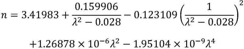
- the refractive index of silicon is greater than 3.41, which is a relatively large value, so silicon can be selected as the base material of the microlens in this wavelength band.
- the dispersion formula of silicon is as follows:
- silicon is used as the material of the dielectric substrate 101.
- silicon has good light transmission and high refractive index.
- the specific imaging rule satisfies the following expression:
- R 1 is the radius of curvature of the spherical end of the flat-concave air cavity 102, and the radius of curvature R 1 ⁇ [20 ⁇ m-200 ⁇ m] of the spherical end of the flat-concave air cavity 102;
- f is the focal length of the microlens based on the high refractive index medium substrate 101 (starting to calculate from the plano-concave air cavity 102);
- n si is the refractive index of the dielectric substrate 101
- the microlens based on the high refractive index dielectric substrate 101 with the target focal length can be obtained.
- FIG. 2 is a schematic diagram of optical simulation, wherein the dielectric substrate 101 is silicon, and the incident light is incident on the microlens. At this time,
- the outgoing surface of the dielectric substrate 101 is not connected to the photodetector, specifically the mercury cadmium telluride photodetection component, the wavelength of the incident light is 4 ⁇ m, and the incident light will be focused after passing through the spherical end of the flat-concave air cavity 102 of the microlens, as shown in Fig. 3 is a schematic diagram of the electric field intensity in the cross-section of the imaging focus.
- the full width at half maximum of the focal field strength can be obtained to be smaller than the full width at half maximum defined by the Rayleigh diffraction limit formula.
- the distance from the center of the spherical end of the plano-concave air cavity 102 to the exit surface of the dielectric substrate 101 is defined as L, and L is smaller than the focal length f of the incident light from the spherical end of the plano-concave air cavity 102. It can be understood that , the focal length of the microlens based on the high refractive index dielectric substrate 101 does not fall into the dielectric substrate 101 .
- the outgoing surface of the dielectric substrate 101 is connected to a photodetector, specifically a mercury cadmium telluride photodetector assembly, including components connected to a mercury cadmium telluride medium and a CCD camera.
- the dielectric substrate 101 is made of silicon, and the incident light is incident on the micro Lenses, microlenses based on silicon substrates form a single-lens imaging system that can be used for 3 ⁇ m-5 ⁇ m optical imaging and detection.
- the refractive index of mercury cadmium telluride has a great relationship with its material composition.
- Fig. 5 is a simulated field intensity diagram of a mercury cadmium telluride medium connected to the exit surface
- Fig. 6 is a schematic diagram of the electric field intensity of the imaging focus cross-section after the mercury cadmium telluride medium is connected. The effect does not change much, and the size of the focal spot can still achieve a smaller diffraction limit.
- the CCD camera Through the connected CCD camera, the imaged image can be output to the device.
Landscapes
- Physics & Mathematics (AREA)
- General Physics & Mathematics (AREA)
- Optics & Photonics (AREA)
- Engineering & Computer Science (AREA)
- Power Engineering (AREA)
- Electromagnetism (AREA)
- Condensed Matter Physics & Semiconductors (AREA)
- Computer Hardware Design (AREA)
- Microelectronics & Electronic Packaging (AREA)
- Optical Head (AREA)
- Solid State Image Pick-Up Elements (AREA)
- Lenses (AREA)
Abstract
A micro-lens based on a high-refractive-index dielectric substrate, comprising a light-transmitting dielectric substrate (101). The dielectric substrate (101) has an incident surface for incident light to be incident on, and a wavelength λ of incident light is [2.5 μm‑25 μm]. The dielectric substrate (101) has an emergent surface and a plano-concave air cavity (102), and the plano-concave air cavity (102) is formed in the dielectric substrate (101). One end of the plano-concave air cavity (102) is a planar end facing the incident surface, and the other end is a spherical end having a notch shape and the notch facing the emergent surface, so that the incident light is focused into a focus after passing through the plano-concave air cavity (102), and thus the full width at half maximum of focus field intensity is smaller than the full width at half maximum defined by a Rayleigh diffraction limit formula. The micro-lens is capable of obtaining an Airy disk that is smaller than a Rayleigh criterion in a defined incident wave band.
Description
本发明涉及微纳光学及光学成像技术领域,特别涉及一种基于高折射率介质基底的微透镜。The invention relates to the technical field of micro-nano optics and optical imaging, in particular to a microlens based on a high-refractive-index medium substrate.
透镜的有限孔径尺寸会对入射光线发生衍射,这导致透镜无法把光线会聚成无限小的点,而只会在焦点上形成具有一定能量分布的艾里斑。一般来说,通过任何光学仪器成像的过程都可以认为是把物体上的无数微小的点转换成艾里斑图案,然后再把它们叠加起来,所以,所成的像无法精确地描述物体的所有细节。当两个艾里斑的最小可分辨距离为一个圆斑中心与另一个圆斑边缘重合的时候,该距离也叫做瑞利判据。透镜的成像像点大小受限于瑞利判据,即0 .61λ/NA,该公式表明,光束在进行聚焦时所得到的聚焦光斑尺寸在半波长以上。因此,这阻碍了在超分辨成像和光刻中进一步增强分辨本领。而传统的增强分辨能力方案是缩小波长或增大透镜尺寸。The finite aperture size of the lens will diffract the incident light, which makes the lens unable to converge the light into an infinitely small point, but only forms an Airy disk with a certain energy distribution at the focal point. Generally speaking, the process of imaging through any optical instrument can be considered as converting countless tiny points on the object into Airy disk patterns, and then superimposing them, so the formed image cannot accurately describe all the objects. detail. When the minimum resolvable distance between two Airy disks is that the center of one circular spot coincides with the edge of the other circular spot, this distance is also called the Rayleigh criterion. The imaging point size of the lens is limited by the Rayleigh criterion, that is, 0.61λ/NA. This formula indicates that the focused spot size obtained when the beam is focused is above half the wavelength. Therefore, this hinders further enhancement of resolving power in super-resolution imaging and lithography. The traditional solution to enhance the resolution is to reduce the wavelength or increase the size of the lens.
本发明旨在至少在一定程度上解决现有技术中的上述技术问题之一。为此,本发明实施例提供一种基于高折射率介质基底的微透镜,能够在限定的入射波段中,得到比瑞利判据更小的艾里斑。The present invention aims to solve one of the above-mentioned technical problems in the prior art at least to a certain extent. Therefore, an embodiment of the present invention provides a microlens based on a high-refractive-index dielectric substrate, which can obtain an Airy disc smaller than the Rayleigh criterion in a limited incident wavelength band.
根据本发明实施例的基于高折射率介质基底的微透镜,包括透光的介质基底,所述介质基底具有入射面,以供入射光线射入,入射光线的波长λ∈[2 .5μm‑25μm],所述介质基底具有出射面;以及平凹空气腔,所述平凹空气腔设置于所述介质基底内,所述平凹空气腔一端为平面端,另一端为呈凹口的球面端,所述平凹空气腔的平面端朝向所述入射面,所述平凹空气腔的球面端的凹口朝向所述出射面,以使入射光线通过所述平凹空气腔后聚焦成焦点,从而使焦点场强的半高全宽大小小于瑞利衍射极限公式所定义的半高全宽大小。A microlens based on a high-refractive-index dielectric substrate according to an embodiment of the present invention includes a light-transmitting dielectric substrate, the dielectric substrate has an incident surface for incident light to enter, and the wavelength λ∈[2.5 μm-25 μm of the incident light ], the medium substrate has an exit surface; and a flat-concave air cavity, the flat-concave air cavity is arranged in the medium substrate, one end of the flat-concave air cavity is a plane end, and the other end is a notched spherical end , the planar end of the flat concave air cavity faces the incident surface, and the notch of the spherical end of the flat concave air cavity faces the outgoing surface, so that the incident light is focused into a focal point after passing through the flat concave air cavity, so that Make the full width at half maximum of the focal field strength smaller than the full width at half maximum defined by the Rayleigh diffraction limit formula.
在可选或优选的实施例中,入射光线的波长λ∈[3μm‑5μm]。In an optional or preferred embodiment, the incident light has a wavelength λ∈[3μm-5μm].
在可选或优选的实施例中,所述平凹空气腔的球面端中心到介质基底的出射面的距离定义为L,所述L小于入射光线从所述平凹空气腔的球面端入射的焦距f。In an optional or preferred embodiment, the distance from the center of the spherical end of the flat concave air cavity to the exit surface of the medium substrate is defined as L, and the L is smaller than the distance of the incident light from the spherical end of the flat concave air cavity focal length f.
在可选或优选的实施例中,所述平凹空气腔的球面端的曲率半径R
1∈[20μm‑200μ m]。
In an optional or preferred embodiment, the radius of curvature R 1 ε[20μm-200μm] of the spherical end of the plano-concave air cavity.
在可选或优选的实施例中,所述介质基底的入射面镀有增透膜。In an optional or preferred embodiment, the incident surface of the dielectric substrate is coated with an anti-reflection film.
在可选或优选的实施例中,所述介质基底的出射面连接有光电探测器。In an optional or preferred embodiment, a photodetector is connected to the exit surface of the dielectric substrate.
在可选或优选的实施例中,所述介质基底为圆柱体,所述入射面和所述出射面分别位于圆柱体的两个端面。In an optional or preferred embodiment, the medium substrate is a cylinder, and the incident surface and the outgoing surface are respectively located on two end surfaces of the cylinder.
在可选或优选的实施例中,所述介质基底的材质为硅或锗的其中一种。In an optional or preferred embodiment, the material of the dielectric substrate is one of silicon and germanium.
在可选或优选的实施例中,所述介质基底的折射率大于2 .0。In an optional or preferred embodiment, the refractive index of the dielectric substrate is greater than 2.0.
在可选或优选的实施例中,成像规律满足如下的表达式为:In an optional or preferred embodiment, the imaging law satisfies the following expression:

其中,R
1是所述平凹空气腔球面端的曲率半径;f是所述基于高折射率介质基底的微透镜的焦距(从所述平凹空气腔处开始计算) ;n是所述介质基底的折射率;通过选取R
1值,以获得目标焦距的基于高折射率介质基底的微透镜。
Wherein, R 1 is the radius of curvature of the spherical end of the flat concave air cavity; f is the focal length of the microlens based on the high refractive index medium substrate (starting to calculate from the flat concave air cavity); n is the medium substrate The refractive index; by selecting the R 1 value, the microlens based on the high refractive index medium substrate with the target focal length is obtained.
基于上述技术方案,本发明实施例至少具有以下有益效果:上述技术方案,通过在介质基底中设置平凹空气腔,平凹空气腔的平面端朝向介质基底的入射面,平凹空气腔的球面端的凹口朝向介质基底的出射面,限定波段范围的入射光线射入介质基底中,经过平凹空气腔后聚焦成焦点,焦点场强的半高全宽大小小于瑞利衍射极限公式所定义的半高全宽大小,实现比瑞利判据更小的艾里斑,打破了现有的成像极限。本发明基于高折射率介质基底的微透镜可用于光学成像与探测,在微纳光学领域有着广泛的应用前景。Based on the above technical solution, the embodiments of the present invention have at least the following beneficial effects: in the above technical solution, by setting a flat concave air cavity in the medium substrate, the plane end of the flat concave air cavity faces the incident surface of the medium substrate, and the spherical surface of the flat concave air cavity The notch at the end faces the exit surface of the medium substrate, and the incident light with a limited wavelength range enters the medium substrate and is focused into a focal point after passing through the flat concave air cavity. The full width at half maximum of the focal field strength is smaller than the full width at half maximum defined by the Rayleigh diffraction limit formula size, achieving an Airy disk smaller than the Rayleigh criterion, breaking the existing imaging limit. The microlens based on the high refractive index medium substrate of the present invention can be used for optical imaging and detection, and has broad application prospects in the field of micro-nano optics.
下面结合附图和实施例对本发明进一步地说明;Below in conjunction with accompanying drawing and embodiment the present invention is further described;
图1是本发明实施例的截面图,其中未绘出剖物线;Fig. 1 is a sectional view of an embodiment of the present invention, wherein the hatch line is not drawn;
图2是本发明实施例的光学仿真示意图;Fig. 2 is the optical simulation schematic diagram of the embodiment of the present invention;
图3是本发明实施例的成像焦点横截面的电场强度示意图;Fig. 3 is a schematic diagram of the electric field intensity of the imaging focus cross-section of the embodiment of the present invention;
图4是本发明实施例的成像焦点大小变化的仿真曲线和理论瑞利判据衍射极限的Fig. 4 is the simulation curve of the imaging focus size variation of the embodiment of the present invention and the theoretical Rayleigh criterion diffraction limit
对比图;comparison chart;
图5是本发明实施例接碲镉汞介质后的仿真示意图;Fig. 5 is the emulation schematic diagram of the embodiment of the present invention connected with HgCdTe medium;
图6是本发明实施例接碲镉汞介质后的成像焦点横截面的电场强度示意图;Fig. 6 is a schematic diagram of the electric field intensity of the imaging focus cross-section after the embodiment of the present invention is connected to the HgCdTe medium;
图7是基于26℃环境下硅的折射率随波长变化示意图。Fig. 7 is a schematic diagram of the change of the refractive index of silicon with wavelength based on the environment of 26°C.
本部分将详细描述本发明的具体实施例,本发明之较佳实施例在附图中示出,附图的作用在于用图形补充说明书文字部分的描述,使人能够直观地、形象地理解本发明的每个技术特征和整体技术方案,但其不能理解为对本发明保护范围的限制。This part will describe the specific embodiment of the present invention in detail, and the preferred embodiment of the present invention is shown in the accompanying drawings. Each technical feature and overall technical solution of the invention, but it should not be understood as a limitation on the protection scope of the present invention.
在本发明的描述中,需要理解的是,涉及到方位描述,例如上、下、前、后、左、右等指示的方位或位置关系为基于附图所示的方位或位置关系,仅是为了便于描述本发明和简化描述,而不是指示或暗示所指的装置或元件必须具有特定的方位、以特定的方位构造和操作,因此不能理解为对本发明的限制。In the description of the present invention, it should be understood that the orientation descriptions, such as up, down, front, back, left, right, etc. indicated orientations or positional relationships are based on the orientations or positional relationships shown in the drawings, and are only In order to facilitate the description of the present invention and simplify the description, it does not indicate or imply that the device or element referred to must have a specific orientation, be constructed and operated in a specific orientation, and thus should not be construed as limiting the present invention.
在本发明的描述中,若干的含义是一个或者多个,多个的含义是两个以上,大于、小于、超过等理解为不包括本数,以上、以下、以内等理解为包括本数。如果有描述到第一、第二只是用于区分技术特征为目的,而不能理解为指示或暗示相对重要性或者隐含指明所指示的技术特征的数量或者隐含指明所指示的技术特征的先后关系。In the description of the present invention, several means one or more, and multiple means more than two. Greater than, less than, exceeding, etc. are understood as not including the original number, and above, below, within, etc. are understood as including the original number. If the description of the first and second is only for the purpose of distinguishing the technical features, it cannot be understood as indicating or implying the relative importance or implicitly indicating the number of the indicated technical features or implicitly indicating the order of the indicated technical features relation.
本发明的描述中,除非另有明确的限定,设置、安装、连接等词语应做广义理解,所In the description of the present invention, unless otherwise clearly defined, terms such as installation, installation, and connection should be understood in a broad sense.
属技术领域技术人员可以结合技术方案的具体内容合理确定上述词语在本发明中的具体含义。Those skilled in the art can reasonably determine the specific meanings of the above words in the present invention in combination with the specific content of the technical solution.
参照图1至图7,一种基于高折射率介质基底101的微透镜,包括介质基底101和平1 to 7, a microlens based on a high refractive index dielectric substrate 101, including a dielectric substrate 101 and a flat surface
凹空气腔102。其中,介质基底101是透光的,本实施例选用的介质基底101具有高折射率,具体的,介质基底101的折射率大于2 .0。Concave air cavity 102 . Wherein, the dielectric substrate 101 is transparent, and the dielectric substrate 101 selected in this embodiment has a high refractive index, specifically, the refractive index of the dielectric substrate 101 is greater than 2.0.
介质基底101具有入射面,以供入射光线射入,介质基底101具有出射面。平凹空气腔102一端为平面端,另一端为呈凹口的球面端,平凹空气腔102的平面端朝向入射面,平凹空气腔102的球面端的凹口朝向出射面,以使入射光线通过平凹空气腔102后聚焦成焦点, 入射光线的波长λ∈[2 .5μm‑25μm],可以使焦点场强的半高全宽大小小于瑞利衍射极限公式所定义的半高全宽大小。更为具体的,入射光线的波长λ∈[3μm‑5μm],可以使焦点场强的半高全宽大小更加理想。The dielectric substrate 101 has an incident surface for incident light to enter, and the dielectric substrate 101 has an outgoing surface. One end of the flat-concave air cavity 102 is a plane end, and the other end is a notched spherical end. The plane end of the flat-concave air cavity 102 faces the incident surface, and the notch of the spherical end of the flat-concave air cavity 102 faces the exit surface, so that the incident light After passing through the plano-concave air cavity 102 and focusing into a focal point, the wavelength λ∈[2.5μm-25μm] of the incident light can make the full width at half maximum of the focal field strength smaller than the full width at half maximum defined by the Rayleigh diffraction limit formula. More specifically, the wavelength λ∈[3μm‑5μm] of the incident light can make the full width at half maximum of the focal field strength more ideal.
在其中的一个实施例中,介质基底101为圆柱体,入射面和出射面分别位于圆柱体的两个端面。介质基底101的入射面镀有增透膜,可以增加入射的光线量,增透膜具体层数视实际所需应用场景决定,本实施例中,增透膜包括第一增透膜201和第二增透膜202。另外,介质基底101的出射面连接有光电探测器。In one of the embodiments, the dielectric substrate 101 is a cylinder, and the incident surface and the outgoing surface are respectively located on two end surfaces of the cylinder. The incident surface of the dielectric substrate 101 is coated with an anti-reflection film, which can increase the amount of incident light. The specific number of layers of the anti-reflection film depends on the actual application scene. In this embodiment, the anti-reflection film includes the first anti-reflection film 201 and the second anti-reflection film. Two antireflection coatings 202 . In addition, a photodetector is connected to the outgoing surface of the dielectric substrate 101 .
介质基底101的材质为硅或锗的其中一种。参照图7,在入射光线的波长λ∈[2 .5μThe material of the dielectric substrate 101 is one of silicon and germanium. Referring to Figure 7, at the wavelength λ∈[2 .5μ of incident light
m‑25μm]的波段内,硅的折射率都大于3 .41,这是一个较大的数值,因此在该波段内都可以选择硅作为所述微透镜的基底材料。In the wavelength band of m-25 μm], the refractive index of silicon is greater than 3.41, which is a relatively large value, so silicon can be selected as the base material of the microlens in this wavelength band.
温度为26℃,波长为2 .5μm‑25μm范围内,硅的色散公式如下:When the temperature is 26°C and the wavelength is in the range of 2.5μm-25μm, the dispersion formula of silicon is as follows:
本实施例采用硅作为介质基底101的材质,在3μm‑5μm波长段,硅具有良好的透光性,并且具有高折射率,具体的成像规律满足如下的表达式为:In this embodiment, silicon is used as the material of the dielectric substrate 101. In the 3 μm-5 μm wavelength range, silicon has good light transmission and high refractive index. The specific imaging rule satisfies the following expression:

其中,R
1是平凹空气腔102球面端的曲率半径,平凹空气腔102的球面端的曲率半径R
1∈ [20μm‑200μm];
Wherein, R 1 is the radius of curvature of the spherical end of the flat-concave air cavity 102, and the radius of curvature R 1 ∈ [20 μm-200 μm] of the spherical end of the flat-concave air cavity 102;
f是基于高折射率介质基底101的微透镜的焦距(从平凹空气腔102处开始计算) ;f is the focal length of the microlens based on the high refractive index medium substrate 101 (starting to calculate from the plano-concave air cavity 102);
n
si是所述介质基底101的折射率;
n si is the refractive index of the dielectric substrate 101;
通过选取R
1值,以获得目标焦距的基于高折射率介质基底101的微透镜。
By selecting the value of R 1 , the microlens based on the high refractive index dielectric substrate 101 with the target focal length can be obtained.
可以理解的是,从上述成像规律的表达式,在确定目标焦距f参数后,可确定出适当的R
1值,从而制造出具有目标焦距的微透镜。
It can be understood that, from the expression of the above imaging law, after determining the target focal length f parameter, an appropriate R 1 value can be determined, thereby manufacturing a microlens with the target focal length.
图2为光学仿真示意图,其中,介质基底101为硅,入射光线正入射到微透镜,此时,FIG. 2 is a schematic diagram of optical simulation, wherein the dielectric substrate 101 is silicon, and the incident light is incident on the microlens. At this time,
介质基底101的出射面不接光电探测器,具体是不接碲镉汞光电探测组件,入射光波长为4μ m,入射光线在经过微透镜的平凹空气腔102球面端后会形成聚焦,图3为成像焦点横截面的电场强度示意图。另外,通过调整微透镜中的平凹空气腔102球面端的曲率半径,可得到焦点场强的半高全宽将小于瑞利衍射极限公式所定义的半高全宽大小。在3μm‑5μm波段范围的入射光线情况下,焦点的半高全宽变化和瑞利衍射分辨极限的变化如图4所示,图4出示了在波长为4μm的入射光线时对应于不同曲面曲率半径的计算结果,可以看到在我们设定的工作波长区间,通过改变微透镜的参数,可以实现焦距的半高全宽小于瑞利衍射极限的效果。The outgoing surface of the dielectric substrate 101 is not connected to the photodetector, specifically the mercury cadmium telluride photodetection component, the wavelength of the incident light is 4 μm, and the incident light will be focused after passing through the spherical end of the flat-concave air cavity 102 of the microlens, as shown in Fig. 3 is a schematic diagram of the electric field intensity in the cross-section of the imaging focus. In addition, by adjusting the radius of curvature of the spherical end of the plano-concave air cavity 102 in the microlens, the full width at half maximum of the focal field strength can be obtained to be smaller than the full width at half maximum defined by the Rayleigh diffraction limit formula. In the case of incident light in the wavelength range of 3μm-5μm, the change of the full width at half maximum of the focal point and the change of the resolution limit of Rayleigh diffraction are shown in Figure 4. From the calculation results, it can be seen that in the working wavelength range we set, by changing the parameters of the microlens, the effect that the full width at half maximum of the focal length can be achieved is smaller than the Rayleigh diffraction limit.
其中的一个实施例,平凹空气腔102的球面端中心到介质基底101的出射面的距离定义为L,L小于入射光线从平凹空气腔102的球面端入射的焦距f,可以理解的是,基于高折射率介质基底101的微透镜的焦距没有落入到介质基底101内。 In one of the embodiments, the distance from the center of the spherical end of the plano-concave air cavity 102 to the exit surface of the dielectric substrate 101 is defined as L, and L is smaller than the focal length f of the incident light from the spherical end of the plano-concave air cavity 102. It can be understood that , the focal length of the microlens based on the high refractive index dielectric substrate 101 does not fall into the dielectric substrate 101 . the
另外的一个实施例中,介质基底101的出射面接光电探测器,具体是碲镉汞光电探测组件,包括接碲镉汞介质和CCD相机等组件,介质基底101为硅,入射光线正入射到微透镜,基于硅基底的微透镜组成了一套可用于3μm‑5μm光学成像与探测的单镜头成像系统。碲镉汞的折射率跟其材料组分有很大关系,我们假设在该光学成像探测系统工作在室温情况下,则当碲镉汞的材料组分为Hg0
.8Cd0 .2Te时,碲镉汞介质的折射率与硅介质基本匹配。图5为在出射面接上碲镉汞介质的仿真场强图,图6为接碲镉汞介质后的成像焦点横截面的电场强度示意图,可以看到在后接碲镉汞介质时,其成像效果变化不大,焦斑大小依然可以实现衍射极限要小。通过后接的CCD相机,可以将成像的图像输出到设备里面。In another embodiment, the outgoing surface of the dielectric substrate 101 is connected to a photodetector, specifically a mercury cadmium telluride photodetector assembly, including components connected to a mercury cadmium telluride medium and a CCD camera. The dielectric substrate 101 is made of silicon, and the incident light is incident on the micro Lenses, microlenses based on silicon substrates form a single-lens imaging system that can be used for 3μm-5μm optical imaging and detection. The refractive index of mercury cadmium telluride has a great relationship with its material composition. We assume that when the optical imaging detection system works at room temperature, when the material composition of mercury cadmium telluride is Hg0
.8Cd0 .2Te, the refractive index of mercury cadmium telluride medium and silicon medium basically match. Fig. 5 is a simulated field intensity diagram of a mercury cadmium telluride medium connected to the exit surface, and Fig. 6 is a schematic diagram of the electric field intensity of the imaging focus cross-section after the mercury cadmium telluride medium is connected. The effect does not change much, and the size of the focal spot can still achieve a smaller diffraction limit. Through the connected CCD camera, the imaged image can be output to the device.
上面结合附图对本发明实施例作了详细说明,但是本发明不限于上述实施例,在所述技术领域普通技术人员所具备的知识范围内,还可以在不脱离本发明宗旨的前提下作出各种变化。The embodiments of the present invention have been described in detail above in conjunction with the accompanying drawings, but the present invention is not limited to the above embodiments. Within the scope of knowledge possessed by those of ordinary skill in the art, various modifications can be made without departing from the gist of the present invention. kind of change.
Claims (10)
- 一种基于高折射率介质基底的微透镜,其特征在于:包括A microlens based on a high refractive index medium substrate, characterized in that: comprising透光的介质基底,所述介质基底具有入射面,以供入射光线射入,入射光线的波长λ∈ [2 .5μm‑25μ m],所述介质基底具有出射面;以及A light-transmitting dielectric substrate, the dielectric substrate has an incident surface for the incident light to enter, the wavelength of the incident light λ∈ [2.5 μm-25 μ m], and the dielectric substrate has an exit surface; and平凹空气腔,所述平凹空气腔设置于所述介质基底内,所述平凹空气腔一端为平面端, 另一端为呈凹口的球面端,所述平凹空气腔的平面端朝向所述入射面,所述平凹空气腔的球面端的凹口朝向所述出射面,以使入射光线通过所述平凹空气腔后聚焦成焦点,从而使焦点场强的半高全宽大小小于瑞利衍射极限公式所定义的半高全宽大小。A flat concave air cavity, the flat concave air cavity is arranged in the medium substrate, one end of the flat concave air cavity is a plane end, The other end is a notched spherical end, the plane end of the flat concave air cavity faces the incident surface, and the notch of the spherical end of the flat concave air cavity faces the outgoing surface, so that the incident light passes through the flat surface. The concave air cavity is then focused into a focal point, so that the full width at half maximum of the focal field strength is smaller than the full width at half maximum defined by the Rayleigh diffraction limit formula.
- 根据权利要求1所述的基于高折射率介质基底的微透镜,其特征在于:入射光线的波长λ∈[3μm‑5μm]。The microlens based on a high refractive index medium substrate according to claim 1, characterized in that: the wavelength λ∈[3μm-5μm] of the incident light.
- 根据权利要求1所述的基于高折射率介质基底的微透镜,其特征在于:所述平凹空气腔的球面端的曲率半径R1∈[20μm‑200μm]。The microlens based on a high refractive index medium substrate according to claim 1, characterized in that: the radius of curvature R1∈[20μm-200μm] of the spherical end of the plano-concave air cavity.
- 根据权利要求1所述的基于高折射率介质基底的微透镜,其特征在于:所述平凹空气The microlens based on high refractive index medium substrate according to claim 1, characterized in that: the plano-concave air腔的球面端中心到介质基底的出射面的距离定义为L,所述L小于入射光线从所述平凹空气腔的球面端入射的焦距f。The distance from the center of the spherical end of the cavity to the exit surface of the dielectric substrate is defined as L, which is smaller than the focal length f of the incident light from the spherical end of the plano-concave air cavity.
- 根据权利要求1所述的基于高折射率介质基底的微透镜,其特征在于:所述介质基底的入射面镀有增透膜。The microlens based on a high refractive index dielectric substrate according to claim 1, wherein the incident surface of the dielectric substrate is coated with an anti-reflection film.
- 根据权利要求5所述的基于高折射率介质基底的微透镜,其特征在于:所述介质基底的出射面连接有光电探测器。The microlens based on a high refractive index dielectric substrate according to claim 5, wherein a photodetector is connected to the outgoing surface of the dielectric substrate.
- 根据权利要求6所述的基于高折射率介质基底的微透镜,其特征在于:所述介质基底为圆柱体,所述入射面和所述出射面分别位于圆柱体的两个端面。The microlens based on a high refractive index dielectric substrate according to claim 6, wherein the dielectric substrate is a cylinder, and the incident surface and the outgoing surface are respectively located on two end surfaces of the cylinder.
- 根据权利要求1至7任意一项所述的基于高折射率介质基底的微透镜,其特征在于: 所述介质基底的折射率大于2 .0。The microlens based on a high refractive index medium substrate according to any one of claims 1 to 7, characterized in that: The refractive index of the dielectric substrate is greater than 2.0.
- 根据权利要求8所述的基于高折射率介质基底的微透镜,其特征在于:所述介质基底的材质为硅或锗的其中一种。The microlens based on a high refractive index dielectric substrate according to claim 8, wherein the dielectric substrate is made of one of silicon and germanium.
- 根据权利要求8所述的基于高折射率介质基底的微透镜,其特征在于,成像规律满足如下的表达式为:The microlens based on a high refractive index medium substrate according to claim 8, wherein the imaging law satisfies the following expression:
 其中, R 1是所述平凹空气腔球面端的曲率半径; f是所述基于高折射率介质基底的微透镜从所述平凹空气腔处开始计算的焦距 ; n是所述介质基底的折射率;通过选取R1值,以获得目标焦距的基于高折射率介质基底的微透镜。 Wherein, R 1 is the radius of curvature of the spherical end of the plano-concave air cavity; f is the focal length calculated from the plano-concave air cavity by the microlens based on the high refractive index medium substrate; n is the refraction of the medium substrate Rate; By selecting the R1 value, the microlens based on the high refractive index medium substrate with the target focal length is obtained.
Priority Applications (1)
| Application Number | Priority Date | Filing Date | Title |
|---|---|---|---|
| US18/748,104 US20240337777A1 (en) | 2021-08-20 | 2024-06-20 | Micro-lens based on high-refractive-index dielectric substrate |
Applications Claiming Priority (2)
| Application Number | Priority Date | Filing Date | Title |
|---|---|---|---|
| CN202110960195.4A CN113820763B (en) | 2021-08-20 | 2021-08-20 | Micro-lens based on high-refractive-index medium substrate |
| CN202110960195.4 | 2021-12-21 |
Related Child Applications (1)
| Application Number | Title | Priority Date | Filing Date |
|---|---|---|---|
| US18/748,104 Continuation US20240337777A1 (en) | 2021-08-20 | 2024-06-20 | Micro-lens based on high-refractive-index dielectric substrate |
Publications (1)
| Publication Number | Publication Date |
|---|---|
| WO2023116201A1 true WO2023116201A1 (en) | 2023-06-29 |
Family
ID=78922940
Family Applications (1)
| Application Number | Title | Priority Date | Filing Date |
|---|---|---|---|
| PCT/CN2022/128464 WO2023116201A1 (en) | 2021-08-20 | 2022-10-30 | Micro-lens based on high-refractive-index dielectric substrate |
Country Status (3)
| Country | Link |
|---|---|
| US (1) | US20240337777A1 (en) |
| CN (1) | CN113820763B (en) |
| WO (1) | WO2023116201A1 (en) |
Families Citing this family (1)
| Publication number | Priority date | Publication date | Assignee | Title |
|---|---|---|---|---|
| CN113820763B (en) * | 2021-08-20 | 2022-10-25 | 华南理工大学 | Micro-lens based on high-refractive-index medium substrate |
Citations (6)
| Publication number | Priority date | Publication date | Assignee | Title |
|---|---|---|---|---|
| US20040108476A1 (en) * | 2002-12-06 | 2004-06-10 | Ultra-Scan Corporation | Method for optimizing performance of optical encoders operating in a fluid |
| US20060088244A1 (en) * | 2004-10-25 | 2006-04-27 | Rpo Pty Limited | Planar lenses for integrated optics |
| CN201084461Y (en) * | 2007-08-09 | 2008-07-09 | 中国科学院长春光学精密机械与物理研究所 | A variable-focus X-ray lens combination |
| CN109713055A (en) * | 2017-10-20 | 2019-05-03 | 英飞凌科技德累斯顿公司 | Lenticule with DNAcarrier free optical interference filter |
| RU2744033C1 (en) * | 2020-06-01 | 2021-03-02 | Федеральное государственное бюджетное образовательное учреждение высшего образования "Сибирский государственный университет геосистем и технологий" | Ehf varifocal lens |
| CN113820763A (en) * | 2021-08-20 | 2021-12-21 | 华南理工大学 | Micro-lens based on high-refractive-index medium substrate |
Family Cites Families (8)
| Publication number | Priority date | Publication date | Assignee | Title |
|---|---|---|---|---|
| JP3677342B2 (en) * | 1996-02-23 | 2005-07-27 | 松下電器産業株式会社 | Optical head device and optical disk device |
| CN100444381C (en) * | 2006-10-13 | 2008-12-17 | 中国科学院上海技术物理研究所 | Backward integrated micro-lens infrared focal plane detector and micro-lens producing method |
| US8003965B2 (en) * | 2007-05-18 | 2011-08-23 | The Regents Of The University Of Michigan | Apparatus for sub-wavelength near-field focusing of electromagnetic waves |
| CN104089701B (en) * | 2010-05-07 | 2016-11-09 | 台湾超微光学股份有限公司 | Optical system |
| US9529203B2 (en) * | 2012-09-17 | 2016-12-27 | Cytonome/St, Llc | Focal plane shifting system |
| CN103969710B (en) * | 2014-04-04 | 2016-05-04 | 南京邮电大学 | The symmetrical vector light beam focusing plano-concave of one-dimensional metal photon crystals post mirror |
| CN108535865A (en) * | 2018-05-23 | 2018-09-14 | 南京邮电大学 | A kind of negative refraction grating plano-concave mirror design method that focal length is controllable |
| CN111999786A (en) * | 2020-09-11 | 2020-11-27 | 电子科技大学 | Hemispherical lens with opaque film covering spherical center and preparation method thereof |
-
2021
- 2021-08-20 CN CN202110960195.4A patent/CN113820763B/en active Active
-
2022
- 2022-10-30 WO PCT/CN2022/128464 patent/WO2023116201A1/en unknown
-
2024
- 2024-06-20 US US18/748,104 patent/US20240337777A1/en active Pending
Patent Citations (6)
| Publication number | Priority date | Publication date | Assignee | Title |
|---|---|---|---|---|
| US20040108476A1 (en) * | 2002-12-06 | 2004-06-10 | Ultra-Scan Corporation | Method for optimizing performance of optical encoders operating in a fluid |
| US20060088244A1 (en) * | 2004-10-25 | 2006-04-27 | Rpo Pty Limited | Planar lenses for integrated optics |
| CN201084461Y (en) * | 2007-08-09 | 2008-07-09 | 中国科学院长春光学精密机械与物理研究所 | A variable-focus X-ray lens combination |
| CN109713055A (en) * | 2017-10-20 | 2019-05-03 | 英飞凌科技德累斯顿公司 | Lenticule with DNAcarrier free optical interference filter |
| RU2744033C1 (en) * | 2020-06-01 | 2021-03-02 | Федеральное государственное бюджетное образовательное учреждение высшего образования "Сибирский государственный университет геосистем и технологий" | Ehf varifocal lens |
| CN113820763A (en) * | 2021-08-20 | 2021-12-21 | 华南理工大学 | Micro-lens based on high-refractive-index medium substrate |
Also Published As
| Publication number | Publication date |
|---|---|
| US20240337777A1 (en) | 2024-10-10 |
| CN113820763A (en) | 2021-12-21 |
| CN113820763B (en) | 2022-10-25 |
Similar Documents
| Publication | Publication Date | Title |
|---|---|---|
| JPH07128589A (en) | Imagery spherical lens for wide field of view | |
| CN110488394A (en) | A kind of LONG WAVE INFRARED complex optics | |
| KR20050010615A (en) | Image sensor and method for fabricating the same | |
| WO2014038541A1 (en) | Infrared imaging optical system | |
| US20240337777A1 (en) | Micro-lens based on high-refractive-index dielectric substrate | |
| TWI393932B (en) | Image capture lens | |
| CN110568590A (en) | Starlight-level optical lens and imaging method thereof | |
| US3843235A (en) | Image forming optical system wherein defocus images are improved | |
| CN110989150A (en) | Large-zoom-ratio optical passive semi-athermal zoom optical system | |
| CN102033316A (en) | Long-wave long-focus uncooled thermalization-free infrared optical system | |
| CN109445069B (en) | Economical infrared athermalized lens and imaging method | |
| CN107797259A (en) | A kind of super clear 4K tight shots of 5.2mm | |
| CN111458843B (en) | Medium wave infrared microscope lens | |
| CN111474683B (en) | High numerical aperture long wave infrared microscope head | |
| CN104459958A (en) | Prime lens used for infrared camera | |
| TW201723575A (en) | Four-piece infrared single wavelength lens assembly | |
| CN211402911U (en) | Large-zoom-ratio optical passive semi-athermal zoom optical system | |
| CN210294661U (en) | Non-focusing full-refraction athermal infrared optical system | |
| TWI710789B (en) | Five-piece infrared single focus lens system | |
| CN110865452B (en) | Airborne medium wave refrigeration infrared continuous zooming optical system | |
| TW201502570A (en) | Imaging optical device | |
| RU2643707C1 (en) | Infrared three-lens objective | |
| RU2629887C1 (en) | High-speed three-lens objective for ir spectrum | |
| TWI857588B (en) | Optical lenses and electronic products | |
| CN109343202A (en) | A kind of full shot |
Legal Events
| Date | Code | Title | Description |
|---|---|---|---|
| 121 | Ep: the epo has been informed by wipo that ep was designated in this application |
Ref document number: 22909518 Country of ref document: EP Kind code of ref document: A1 |
|
| NENP | Non-entry into the national phase |
Ref country code: DE |