WO2023112570A1 - Semiconductor device and power conversion device - Google Patents
Semiconductor device and power conversion device Download PDFInfo
- Publication number
- WO2023112570A1 WO2023112570A1 PCT/JP2022/042064 JP2022042064W WO2023112570A1 WO 2023112570 A1 WO2023112570 A1 WO 2023112570A1 JP 2022042064 W JP2022042064 W JP 2022042064W WO 2023112570 A1 WO2023112570 A1 WO 2023112570A1
- Authority
- WO
- WIPO (PCT)
- Prior art keywords
- semiconductor device
- electrode
- field
- limiting layer
- field plate
- Prior art date
Links
- 239000004065 semiconductor Substances 0.000 title claims abstract description 32
- 238000006243 chemical reaction Methods 0.000 title claims abstract description 14
- 229910021420 polycrystalline silicon Inorganic materials 0.000 claims abstract description 24
- 229920005591 polysilicon Polymers 0.000 claims abstract description 24
- 239000010410 layer Substances 0.000 description 40
- XAGFODPZIPBFFR-UHFFFAOYSA-N aluminium Chemical compound [Al] XAGFODPZIPBFFR-UHFFFAOYSA-N 0.000 description 5
- 229910052782 aluminium Inorganic materials 0.000 description 5
- 238000010586 diagram Methods 0.000 description 5
- 238000000034 method Methods 0.000 description 5
- 230000015556 catabolic process Effects 0.000 description 3
- 239000011229 interlayer Substances 0.000 description 3
- 238000011156 evaluation Methods 0.000 description 2
- 239000000463 material Substances 0.000 description 2
- 230000005012 migration Effects 0.000 description 2
- 238000013508 migration Methods 0.000 description 2
- 238000005260 corrosion Methods 0.000 description 1
- 230000007797 corrosion Effects 0.000 description 1
- 230000008878 coupling Effects 0.000 description 1
- 238000010168 coupling process Methods 0.000 description 1
- 238000005859 coupling reaction Methods 0.000 description 1
- 230000000694 effects Effects 0.000 description 1
- 230000005684 electric field Effects 0.000 description 1
- 238000005530 etching Methods 0.000 description 1
- 238000000605 extraction Methods 0.000 description 1
- 238000002844 melting Methods 0.000 description 1
- 230000008018 melting Effects 0.000 description 1
- 238000012986 modification Methods 0.000 description 1
- 230000004048 modification Effects 0.000 description 1
- 238000000059 patterning Methods 0.000 description 1
- 238000000206 photolithography Methods 0.000 description 1
- 239000000758 substrate Substances 0.000 description 1
Images


Classifications
-
- H—ELECTRICITY
- H01—ELECTRIC ELEMENTS
- H01L—SEMICONDUCTOR DEVICES NOT COVERED BY CLASS H10
- H01L29/00—Semiconductor devices adapted for rectifying, amplifying, oscillating or switching, or capacitors or resistors with at least one potential-jump barrier or surface barrier, e.g. PN junction depletion layer or carrier concentration layer; Details of semiconductor bodies or of electrodes thereof ; Multistep manufacturing processes therefor
- H01L29/02—Semiconductor bodies ; Multistep manufacturing processes therefor
- H01L29/06—Semiconductor bodies ; Multistep manufacturing processes therefor characterised by their shape; characterised by the shapes, relative sizes, or dispositions of the semiconductor regions ; characterised by the concentration or distribution of impurities within semiconductor regions
-
- H—ELECTRICITY
- H01—ELECTRIC ELEMENTS
- H01L—SEMICONDUCTOR DEVICES NOT COVERED BY CLASS H10
- H01L29/00—Semiconductor devices adapted for rectifying, amplifying, oscillating or switching, or capacitors or resistors with at least one potential-jump barrier or surface barrier, e.g. PN junction depletion layer or carrier concentration layer; Details of semiconductor bodies or of electrodes thereof ; Multistep manufacturing processes therefor
- H01L29/40—Electrodes ; Multistep manufacturing processes therefor
- H01L29/41—Electrodes ; Multistep manufacturing processes therefor characterised by their shape, relative sizes or dispositions
-
- H—ELECTRICITY
- H01—ELECTRIC ELEMENTS
- H01L—SEMICONDUCTOR DEVICES NOT COVERED BY CLASS H10
- H01L29/00—Semiconductor devices adapted for rectifying, amplifying, oscillating or switching, or capacitors or resistors with at least one potential-jump barrier or surface barrier, e.g. PN junction depletion layer or carrier concentration layer; Details of semiconductor bodies or of electrodes thereof ; Multistep manufacturing processes therefor
- H01L29/66—Types of semiconductor device ; Multistep manufacturing processes therefor
- H01L29/68—Types of semiconductor device ; Multistep manufacturing processes therefor controllable by only the electric current supplied, or only the electric potential applied, to an electrode which does not carry the current to be rectified, amplified or switched
- H01L29/70—Bipolar devices
- H01L29/72—Transistor-type devices, i.e. able to continuously respond to applied control signals
- H01L29/739—Transistor-type devices, i.e. able to continuously respond to applied control signals controlled by field-effect, e.g. bipolar static induction transistors [BSIT]
-
- H—ELECTRICITY
- H01—ELECTRIC ELEMENTS
- H01L—SEMICONDUCTOR DEVICES NOT COVERED BY CLASS H10
- H01L29/00—Semiconductor devices adapted for rectifying, amplifying, oscillating or switching, or capacitors or resistors with at least one potential-jump barrier or surface barrier, e.g. PN junction depletion layer or carrier concentration layer; Details of semiconductor bodies or of electrodes thereof ; Multistep manufacturing processes therefor
- H01L29/66—Types of semiconductor device ; Multistep manufacturing processes therefor
- H01L29/68—Types of semiconductor device ; Multistep manufacturing processes therefor controllable by only the electric current supplied, or only the electric potential applied, to an electrode which does not carry the current to be rectified, amplified or switched
- H01L29/76—Unipolar devices, e.g. field effect transistors
- H01L29/772—Field effect transistors
- H01L29/78—Field effect transistors with field effect produced by an insulated gate
-
- H—ELECTRICITY
- H01—ELECTRIC ELEMENTS
- H01L—SEMICONDUCTOR DEVICES NOT COVERED BY CLASS H10
- H01L29/00—Semiconductor devices adapted for rectifying, amplifying, oscillating or switching, or capacitors or resistors with at least one potential-jump barrier or surface barrier, e.g. PN junction depletion layer or carrier concentration layer; Details of semiconductor bodies or of electrodes thereof ; Multistep manufacturing processes therefor
- H01L29/66—Types of semiconductor device ; Multistep manufacturing processes therefor
- H01L29/86—Types of semiconductor device ; Multistep manufacturing processes therefor controllable only by variation of the electric current supplied, or only the electric potential applied, to one or more of the electrodes carrying the current to be rectified, amplified, oscillated or switched
- H01L29/861—Diodes
- H01L29/868—PIN diodes
Definitions
- the present invention relates to semiconductor devices and power converters.
- a power semiconductor has an active region through which current flows and a termination region to maintain the breakdown voltage.
- the termination region has a p-type field limiting layer (in the case of an n-type structure) and a floating field plate (aluminum (Al) electrode) connected to the field limiting layer to maintain a breakdown voltage. .
- Patent Document 1 is a technique for forming the field plate in the termination region from a material other than Al.
- Patent Document 1 discloses that the field plate (115) is made of polysilicon having a higher resistance than Al.
- Patent document 1 aims at preventing migration of Al due to a current flowing through a field plate, not for improving high-temperature and high-humidity bias resistance, which is the object of the present invention.
- Patent Document 1 in order to electrically connect the p-type field limiting layer (114) and the field plate (115), a polysilicon field plate (115) is directly connected to the field limiting layer (114).
- a structure for connecting (Fig. 1) and a structure for connecting the field limiting layer (114) and the field plate (115) through the contact (402) of the aluminum contact electrode (401) without direct connection (Fig. 4, 5) are shown.
- Patent Document 1 shows a structure (FIG. 7) in which a field plate (115) and a field limiting layer (114) form a capacitance via a gate oxide film (108).
- connection structure between the field limiting layer and the field plate has the following problems.
- switching devices such as insulated gate bipolar transistors (IGBTs)
- polysilicon is used as the material for the gate electrode, so there is usually a gate oxide film between the polysilicon and Si, and the polysilicon and the field limiting layer
- IGBTs insulated gate bipolar transistors
- the aluminum contact electrode and the polysilicon are connected to the side walls and the upper part of the polysilicon as shown in FIG. Since contact is made in a small portion, the contact resistance increases.
- Patent Document 1 it is said that the migration of Al can be further suppressed by increasing the contact resistance. Therefore, the above connection method is not suitable for the present invention.
- capacitive coupling is similar to the above, resulting in high resistance (high impedance), which is not a suitable connection method in the present invention.
- Patent Document 1 discloses only a structure with one field limiting layer, and does not discuss the case where there are a plurality of field limiting layers. Also, no consideration has been given to the placement of aluminum contact electrodes within the chip.
- the present invention provides a semiconductor device and a power conversion device using the semiconductor device, which have higher high-temperature and high-humidity bias resistance than conventional ones, and which achieves good connection between the field limiting layer and the field plate. for the purpose.
- One aspect of the semiconductor device of the present invention for solving the above problems is a semiconductor device comprising a floating field limiting layer provided in a termination region, and a field plate electrically connected to the field limiting layer.
- the field plate is made of polysilicon
- the field plate and the field limiting layer are connected via an Al electrode
- the connection between the field limiting layer and the Al electrode and the connection between the field plate and the Al electrode are: It is characterized by being connected by different contacts.
- one aspect of the power conversion device of the present invention is a pair of DC terminals, the same number of AC terminals as the number of phases of the AC output, connected between the pair of DC terminals, and connected in anti-parallel to the switching element and the switching element.
- a power conversion device having two parallel circuits connected in series, the number of switching legs being the same as the number of phases of an AC output, and a gate circuit for controlling a switching element, wherein switching At least one of the element and the diode is characterized by being the above semiconductor device.
- the present invention it is possible to provide a semiconductor device and a power conversion device using the semiconductor device, which have improved high-temperature and high-humidity bias resistance compared to the conventional ones, and also realizes good connection between the field limiting layer and the field plate.
- FIG. 1 A partial enlarged view of FIG. 1 and its cross-sectional view 1 is a circuit diagram showing a schematic configuration of a power converter of the present invention
- FIG. 1 is a top view of the semiconductor device of the present invention
- FIG. 2 is a partially enlarged view of FIG. 1 and its cross-sectional view.
- the upper diagram in FIG. 2 is an enlarged view of the Al electrode group 113 in FIG. 1, and the lower diagram in FIG.
- the semiconductor device 112 of this embodiment has an anode electrode 106 provided in the central active region, and a polysilicon field plate 105 and an Al electrode 108 in the termination region provided on the outer periphery of the active region. have A guard ring 107 is provided on the outer periphery of the termination region.
- an embodiment applied to a diode is described, but the present invention is not limited to this, and may be applied to a switching element such as an IGBT or a MOSFET.
- the termination region comprises, as shown in FIG. 2, a p-type well layer 101 connected to an anode electrode 106 and a plurality of floating p-type field limiters on the surface of the n ⁇ layer substrate 100 to maintain a breakdown voltage.
- a thinning layer 102 and an n+ channel stopper layer 103 formed at the chip edge are provided.
- a p-type well layer 101 extends from the active region and is connected to an anode electrode 106 .
- Channel stopper layer 103 is connected to guard ring electrode 107 .
- the conductivity type (n, p) may be reversed.
- FIG. 2 shows a case where there are four field limiting layers 102, but the number of field limiting layers 102 is not limited as long as it is at least one.
- the field limiting layer 102 in the termination region is electrically connected to the polysilicon field plate 105 through the Al electrode 108.
- the Al electrode 108 is provided only on a part of the polysilicon field plate 105 in order to ensure high temperature and high humidity bias resistance.
- a contact 110 for connecting the Al electrode 108 and the field limiting layer 102 and a contact 109 for connecting the Al electrode 108 and the polysilicon field plate 105 are separately provided. That is, the interlayer film 104a is provided with a contact hole 114 for connecting the Al electrode 108 and the field plate 105 to form a contact 109, and the interlayer films 104a and 104b are provided with the Al electrode 108 and the field limiting layer.
- a contact hole 115 is provided to connect to and constitute a contact 110 .
- there is one contact between one Al electrode 108 and one polysilicon field plate 105 but the number of contacts may be one or more, and may be plural.
- the number of contacts should be one or more, and may be plural.
- a polysilicon extraction region 111 is provided around the contact 110 so that the polysilicon field plate 105 is not provided.
- the Al electrode groups are alternately arranged so that adjacent Al electrodes 108 are not arranged on a straight line. With such a configuration, it is possible to ensure a large distance between the adjacent Al electrodes and prevent the Al electrodes 108 from being corroded and melted due to the potential difference.
- the Al electrode is used to electrically connect the field limiting layer and the polysilicon field plate, but the connection between the field limiting layer and the Al electrode and the connection between the field plate and the Al electrode are different contacts.
- it is possible to reliably contact other than the side wall of the polysilicon field plate and suppress the contact resistance, so that good connection can be realized.
- the electric field applied between the Al electrodes can be relaxed, and high-temperature and high-humidity bias resistance can be ensured.
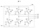
- FIG. 3 is a circuit diagram showing a schematic configuration of the power converter of the present invention.
- FIG. 3 shows an example of the circuit configuration of the power conversion device 500 of this embodiment and the relationship of connection between the DC power supply and the three-phase AC motor (AC load).
- AC load three-phase AC motor
- the semiconductor device of the present invention described above is used as any or all of the power switching elements 501-506 and the diodes 521-526.
- the power switching elements 501-506 are for example IGBTs and the elements 521-526 are diodes.
- the power conversion device 500 of the present embodiment includes a pair of DC terminals, namely, a P terminal 531 and an N terminal 532, and the same number of AC terminals as the number of AC output phases, a U terminal 533 and a V terminal. 534 and a W terminal 535 .
- It also has a switching leg that consists of a pair of power switching elements 501 and 502 connected in series, and that outputs a U terminal 533 connected to the series connection point. It also has a switching leg which is composed of a series connection of power switching elements 503 and 504 having the same configuration and outputs a V terminal 534 connected to the series connection point. A switching leg is also provided, which is composed of a series connection of power switching elements 505 and 506 having the same configuration and has a W terminal 535 connected to the series connection point as an output.
- a three-phase switching leg consisting of power switching elements 501 to 506 is connected between DC terminals of P terminal 531 and N terminal 532, and DC power is supplied from a DC power supply (not shown).
- a U terminal 533, a V terminal 534, and a W terminal 535, which are three-phase AC terminals of the power converter 500, are connected to a three-phase AC motor (not shown) as a three-phase AC power supply.
- a power switching element 501 and a diode 521 connected in antiparallel to the power switching element 501 are connected to form a parallel circuit.
- power switching element 502 and diode 522, power switching element 503 and diode 523, power switching element 504 and diode 524, power switching element 505 and diode 525, and power switching element 506 and diode 526 form a parallel circuit. It is connected to the.
- a parallel circuit including power switching element 501 and a parallel circuit including power switching element 502 are connected in series.
- a parallel circuit including power switching element 503 and a parallel circuit including power switching element 504 are connected in series
- a parallel circuit including power switching element 505 and a parallel circuit including power switching element 506 are connected in series. It is connected.
- Gate circuits 511 to 516 are connected to the input terminals of the gates of the power switching elements 501 to 506 made of IGBTs, and the power switching elements 501 to 506 are controlled by the gate circuits 511 to 516, respectively.
- the gate circuits 511 to 516 are centrally controlled by an overall control circuit (not shown).
- the gate circuits 511 to 516 collectively and appropriately control the power switching elements 501 to 506 to convert the DC power of the DC power supply into three-phase AC power, which is supplied from the U terminal 533, the V terminal 534, and the W terminal 535. output.
- a power conversion device that has higher temperature and humidity bias resistance than the conventional one and realizes a good connection between the field limiting layer and the field plate can be obtained. can provide.
- a semiconductor device capable of improving high-temperature and high-humidity bias resistance as compared with the prior art, and achieving good connection between the field limiting layer and the field plate, and power conversion using the semiconductor device. It was shown that the device can be provided.
- the present invention is not limited to the above-described embodiments, and includes various modifications.
- the above-described embodiments have been described in detail in order to explain the present invention in an easy-to-understand manner, and are not necessarily limited to those having all the described configurations.
- it is possible to replace part of the configuration of one embodiment with the configuration of another embodiment and it is also possible to add the configuration of another embodiment to the configuration of one embodiment.
Abstract
The present invention provides: a semiconductor device which has higher resistance to bias at high temperatures and high humidities than ever before, while achieving good connection between a field limiting layer and a field plate; and a power conversion device which uses this semiconductor device. A semiconductor device according to the present invention is characterized by comprising a floating field limiting layer 102 that is provided in a termination region and a field plate 105 that is electrically connected to the field limiting layer 102, and is also characterized in that: the field plate 105 is formed of a polysilicon; the field plate 105 and the field limiting layer 102 are connected to each other via an Al electrode 108; and the connection between the field limiting layer 102 and the Al electrode 108 and the connection between the field plate 105 and the Al electrode 108 are established at different contacts 109 and 110.
Description
本発明は、半導体装置および電力変換装置に関する。
The present invention relates to semiconductor devices and power converters.
パワー半導体は、様々な過酷な環境で使用されるため、多くの信頼性評価項目を満たす必要がある。信頼性評価項目の1つとして高温高湿バイアス耐性がある。パワー半導体には、電流を流すアクティブ領域と耐圧を保持するためのターミネーション領域がある。ターミネーション領域は、耐圧を保持するためにp型のフィールドリミッティング層(n型構造の場合)と、フィールドリミッティング層に接続されたフローティングのフィールドプレート(アルミニウム(Al)電極)を有している。
Because power semiconductors are used in various harsh environments, they must satisfy many reliability evaluation items. One of the reliability evaluation items is high-temperature and high-humidity bias resistance. A power semiconductor has an active region through which current flows and a termination region to maintain the breakdown voltage. The termination region has a p-type field limiting layer (in the case of an n-type structure) and a floating field plate (aluminum (Al) electrode) connected to the field limiting layer to maintain a breakdown voltage. .
従来のパワー半導体においては、高温高湿環境にて、ターミネーション領域に水分が侵入した状態で、フィールドプレートであるAl電極間に電圧が印加されることで、Al電極が腐食・融解し耐圧保持ができなくなったり、リーク電流が増大するといった課題があった。
In a conventional power semiconductor, in a high-temperature and high-humidity environment, when a voltage is applied between the Al electrodes, which are field plates, with moisture intruding into the termination region, the Al electrodes corrode and melt, and the withstand voltage cannot be maintained. However, there was a problem that the leakage current increased.
ターミネーション領域のフィールドプレートをAl以外の材料で構成する技術として、例えば特許文献1がある。特許文献1には、フィールドプレート(115)をAlより高抵抗のポリシリコンで形成することが示されている。特許文献1は、本発明の目的である高温高湿バイアス耐性を向上させるためではなく、フィールドプレートに流れる電流によるAlのマイグレーションを防ぐことを目的としている。
Patent Document 1, for example, is a technique for forming the field plate in the termination region from a material other than Al. Patent Document 1 discloses that the field plate (115) is made of polysilicon having a higher resistance than Al. Patent document 1 aims at preventing migration of Al due to a current flowing through a field plate, not for improving high-temperature and high-humidity bias resistance, which is the object of the present invention.
また、特許文献1には、p型のフィールドリミッティング層(114)とフィールドプレート(115)を電気的に接続するため、ポリシリコンのフィールドプレート(115)をフィールドリミッティング層(114)と直接接続する構造(図1)と、直接接続せずにアルミコンタクト電極(401)のコンタクト(402)を介してフィールドリミッティング層(114)とフィールドプレート(115)とを接続する構造(図4、図5)とが示されている。また、特許文献1には、ゲート酸化膜(108)を介してフィールドプレート(115)とフィールドリミッティング層(114)とで容量を形成する構造(図7)が示されている。
In addition, in Patent Document 1, in order to electrically connect the p-type field limiting layer (114) and the field plate (115), a polysilicon field plate (115) is directly connected to the field limiting layer (114). A structure for connecting (Fig. 1) and a structure for connecting the field limiting layer (114) and the field plate (115) through the contact (402) of the aluminum contact electrode (401) without direct connection (Fig. 4, 5) are shown. Further, Patent Document 1 shows a structure (FIG. 7) in which a field plate (115) and a field limiting layer (114) form a capacitance via a gate oxide film (108).
上述した特許文献1において、本発明者はフィールドリミッティング層とフィールドプレートとの接続構造に関して以下の課題点があると考えた。Insulated Gate Bipolar Transistor(IGBT)等のスイッチングデバイスにおいては、ポリシリコンはゲート電極の材料として用いられるため、通常ポリシリコンとSiの間には、ゲート酸化膜が存在し、ポリシリコンとフィールドリミッティング層を直接接続するためには、ゲート酸化膜を含むフィールド酸化膜を加工するために、フォトリソグラフィーおよびエッチング工程を含むパターニングを別途追加する必要がある。
In the above-mentioned Patent Document 1, the inventors considered that the connection structure between the field limiting layer and the field plate has the following problems. In switching devices such as insulated gate bipolar transistors (IGBTs), polysilicon is used as the material for the gate electrode, so there is usually a gate oxide film between the polysilicon and Si, and the polysilicon and the field limiting layer In order to connect directly, it is necessary to additionally add patterning including photolithography and etching processes in order to process the field oxide film including the gate oxide film.
また、アルミコンタクト電極を介してフィールドリミッティング層とポリシリコンのフィールドプレートを接続する構造の場合、アルミコンタクト電極とポリシリコンが、特許文献1の図5のように、ポリシリコンの側壁や上部のわずかな一部でコンタクトをとることになるため、コンタクト抵抗が高くなる。特許文献1では、コンタクト抵抗が高くなることで、Alのマイグレーションが更に抑制できるとしているが、本発明においては、フィールドリミッティング層とポリシリコンの接合抵抗を高くする必要はなく、確実にコンタクトをとることを目的とするため、本発明においては、上記の接続方法は好適ではない。
Further, in the case of a structure in which the field limiting layer and the polysilicon field plate are connected via an aluminum contact electrode, the aluminum contact electrode and the polysilicon are connected to the side walls and the upper part of the polysilicon as shown in FIG. Since contact is made in a small portion, the contact resistance increases. In Patent Document 1, it is said that the migration of Al can be further suppressed by increasing the contact resistance. Therefore, the above connection method is not suitable for the present invention.
また、容量結合も上記と同様で、高抵抗(高インピーダンス)となり、本発明においては好適な接続方法ではない。
Also, capacitive coupling is similar to the above, resulting in high resistance (high impedance), which is not a suitable connection method in the present invention.
さらに、特許文献1では、フィールドリミッティング層が1つの構造のみを開示しており、フィールドリミッティング層が複数ある場合に関する検討はなされていない。また、チップ内でのアルミコンタクト電極の配置に関する検討もなされてはいない。
Furthermore, Patent Document 1 discloses only a structure with one field limiting layer, and does not discuss the case where there are a plurality of field limiting layers. Also, no consideration has been given to the placement of aluminum contact electrodes within the chip.
本発明は、上記事情に鑑み、従来よりも高温高湿バイアス耐性を高め、かつ、フィールドリミッティング層とフィールドプレートとの良好な接続も実現する半導体装置およびそれを用いた電力変換装置を提供することを目的とする。
SUMMARY OF THE INVENTION In view of the above circumstances, the present invention provides a semiconductor device and a power conversion device using the semiconductor device, which have higher high-temperature and high-humidity bias resistance than conventional ones, and which achieves good connection between the field limiting layer and the field plate. for the purpose.
上記課題を解決するための本発明の半導体装置一態様は、ターミネーション領域に設けられたフローティングのフィールドリミッティング層と、フィールドリミッティング層に電気的に接続されたフィールドプレートと、を備える半導体装置において、フィールドプレートはポリシリコンにより形成され、フィールドプレートとフィールドリミッティング層はAl電極を介して接続されており、フィールドリミッティング層とAl電極との接続と、フィールドプレートとAl電極との接続は、異なるコンタクトで接続されていることを特徴とする。
One aspect of the semiconductor device of the present invention for solving the above problems is a semiconductor device comprising a floating field limiting layer provided in a termination region, and a field plate electrically connected to the field limiting layer. , the field plate is made of polysilicon, the field plate and the field limiting layer are connected via an Al electrode, and the connection between the field limiting layer and the Al electrode and the connection between the field plate and the Al electrode are: It is characterized by being connected by different contacts.
また、本発明の電力変換装置の一態様は、一対の直流端子と、交流出力の相数と同数の交流端子と、一対の直流端子間に接続され、スイッチング素子とスイッチング素子に逆並列に接続されたダイオードとで構成された並列回路が2個直列に接続された、交流出力の相数と同数のスイッチングレッグと、スイッチング素子を制御するゲート回路と、を有する電力変換装置であって、スイッチング素子およびダイオードの少なくとも一方は、上記半導体装置であることを特徴とする。
Further, one aspect of the power conversion device of the present invention is a pair of DC terminals, the same number of AC terminals as the number of phases of the AC output, connected between the pair of DC terminals, and connected in anti-parallel to the switching element and the switching element. A power conversion device having two parallel circuits connected in series, the number of switching legs being the same as the number of phases of an AC output, and a gate circuit for controlling a switching element, wherein switching At least one of the element and the diode is characterized by being the above semiconductor device.
本発明のより具体的な構成は、特許請求の範囲に記載される。
A more specific configuration of the present invention is described in the claims.
本発明によれば、従来よりも高温高湿バイアス耐性を高め、かつ、フィールドリミッティング層とフィールドプレートとの良好な接続も実現する半導体装置およびそれを用いた電力変換装置を提供できる。
According to the present invention, it is possible to provide a semiconductor device and a power conversion device using the semiconductor device, which have improved high-temperature and high-humidity bias resistance compared to the conventional ones, and also realizes good connection between the field limiting layer and the field plate.
上記した以外の課題、構成及び効果は、以下の実施形態の説明により明らかにされる。
Problems, configurations, and effects other than those described above will be clarified by the following description of the embodiments.
以下、本発明の実施例を、図面を用いて詳細に説明する。
Hereinafter, embodiments of the present invention will be described in detail with reference to the drawings.
図1は本発明の半導体装置の上面図であり、図2は図1の部分拡大図とその断面図である。図2の上図は図1のAl電極群113の拡大図であり、図2の下図は図2の上図のA-A´線断面図である。図1に示すように、本実施例の半導体装置112は、中央のアクティブ領域に設けられたアノード電極106と、アクティブ領域の外周に設けられたターミネーション領域に、ポリシリコンフィールドプレート105およびAl電極108を有する。ターミネーション領域の外周には、ガードリング107が設けられている。なお、本実施例においては、ダイオードに適用した実施例を説明しているが、これに限定されるものではなく、IGBTやMOSFETなどのスイッチング素子に適用してもよい。
FIG. 1 is a top view of the semiconductor device of the present invention, and FIG. 2 is a partially enlarged view of FIG. 1 and its cross-sectional view. The upper diagram in FIG. 2 is an enlarged view of the Al electrode group 113 in FIG. 1, and the lower diagram in FIG. As shown in FIG. 1, the semiconductor device 112 of this embodiment has an anode electrode 106 provided in the central active region, and a polysilicon field plate 105 and an Al electrode 108 in the termination region provided on the outer periphery of the active region. have A guard ring 107 is provided on the outer periphery of the termination region. In addition, in this embodiment, an embodiment applied to a diode is described, but the present invention is not limited to this, and may be applied to a switching element such as an IGBT or a MOSFET.
ターミネーション領域は、図2に示すように、n-層基板100の表面に、耐圧を保持するために、アノード電極106に接続されたp型ウェル層101と、複数のフローティングのp型のフィールドリミッティング層102と、チップ端部に形成されたn+のチャネルストッパ層103が設けられている。アクティブ領域からp型ウェル層101が延伸し、アノード電極106に接続されている。チャネルストッパ層103は、ガードリング電極107に接続されている。なお、導電型(n,p)は反転しても良い。図2では、フィールドリミッティング層102が4つある場合を示しているが、フィールドリミッティング層102の数は少なくとも1つあれば良く、数は限られない。
The termination region comprises, as shown in FIG. 2, a p-type well layer 101 connected to an anode electrode 106 and a plurality of floating p-type field limiters on the surface of the n− layer substrate 100 to maintain a breakdown voltage. A thinning layer 102 and an n+ channel stopper layer 103 formed at the chip edge are provided. A p-type well layer 101 extends from the active region and is connected to an anode electrode 106 . Channel stopper layer 103 is connected to guard ring electrode 107 . Note that the conductivity type (n, p) may be reversed. FIG. 2 shows a case where there are four field limiting layers 102, but the number of field limiting layers 102 is not limited as long as it is at least one.
ターミネーション領域中のフィールドリミッティング層102は、Al電極108を介して、ポリシリコンフィールドプレート105と電気的に接続されている。ここで、高温高湿バイアス耐性を確保するため、Al電極108はポリシリコンフィールドプレート105の一部のみに設けられている。本実施例では、Al電極108とフィールドリミッティング層102とを接続するためのコンタクト110と、Al電極108とポリシリコンフィールドプレート105とを接続するためのコンタクト109を別に設けている。すなわち、層間膜104aにはAl電極108とフィールドプレート105とを接続するためのコンタクトホール114が設けられてコンタクト109を構成し、層間膜104aおよび層間膜104bにはAl電極108とフィールドリミッティング層とを接続するためのコンタクトホール115が設けられてコンタクト110を構成している。なお、図2では1つのAl電極108と1つのポリシリコンフィールドプレート105とのコンタクトが1つであるが、コンタクトの数は1つ以上あれば良く、複数あっても良い。同様に、Al電極108と1つのフィールドリミッティング層102とのコンタクトが1つであるが、コンタクトの数は1つ以上あれば良く、複数あっても良い。
The field limiting layer 102 in the termination region is electrically connected to the polysilicon field plate 105 through the Al electrode 108. Here, the Al electrode 108 is provided only on a part of the polysilicon field plate 105 in order to ensure high temperature and high humidity bias resistance. In this embodiment, a contact 110 for connecting the Al electrode 108 and the field limiting layer 102 and a contact 109 for connecting the Al electrode 108 and the polysilicon field plate 105 are separately provided. That is, the interlayer film 104a is provided with a contact hole 114 for connecting the Al electrode 108 and the field plate 105 to form a contact 109, and the interlayer films 104a and 104b are provided with the Al electrode 108 and the field limiting layer. A contact hole 115 is provided to connect to and constitute a contact 110 . In FIG. 2, there is one contact between one Al electrode 108 and one polysilicon field plate 105, but the number of contacts may be one or more, and may be plural. Similarly, although there is one contact between the Al electrode 108 and one field limiting layer 102, the number of contacts should be one or more, and may be plural.
Al電極108とフィールドリミッティング層102層とを確実に接続するために、コンタクト110の周りは、ポリシリコンフィールドプレート105を設けないように、ポリシリコンの抜き領域111が設けられている。
In order to reliably connect the Al electrode 108 and the field limiting layer 102, a polysilicon extraction region 111 is provided around the contact 110 so that the polysilicon field plate 105 is not provided.
また、図2の上図に示すように、Al電極群は、隣り合うAl電極108が一直線上に配置されないよう、互い違いに配置されている。このような構成とすることで、隣接するAl電極間距離を大きく確保し、電位差によりAl電極108が腐食・融解するのを防止できる。
Also, as shown in the upper diagram of FIG. 2, the Al electrode groups are alternately arranged so that adjacent Al electrodes 108 are not arranged on a straight line. With such a configuration, it is possible to ensure a large distance between the adjacent Al electrodes and prevent the Al electrodes 108 from being corroded and melted due to the potential difference.
本構造によれば、高温高湿バイアス耐性を向上するために、Al電極のフィールドプレートの替りにポリシリコンのフィールドプレートを設けることでAl電極の腐食・融解を避けることができる。また、フィールドリミッティング層とポリシリコンフィールドプレートとを電気的に接続するためにAl電極を用いるが、フィールドリミッティング層とAl電極との接続と、フィールドプレートとAl電極との接続を、異なるコンタクトで接続することで、ポリシリコンフィールドプレートの側壁以外で確実にコンタクトしてコンタクト抵抗を抑えることができるので、良好な接続を実現できる。さらに、Al電極の面積は極力小さくし、かつAl電極領域を互い違いに配置することでAl電極間にかかる電界を緩和し、高温高湿バイアス耐性を確保できる。
According to this structure, corrosion and melting of the Al electrode can be avoided by providing a polysilicon field plate instead of the Al electrode field plate in order to improve high-temperature and high-humidity bias resistance. In addition, the Al electrode is used to electrically connect the field limiting layer and the polysilicon field plate, but the connection between the field limiting layer and the Al electrode and the connection between the field plate and the Al electrode are different contacts. By connecting with , it is possible to reliably contact other than the side wall of the polysilicon field plate and suppress the contact resistance, so that good connection can be realized. Furthermore, by minimizing the area of the Al electrode and arranging the Al electrode regions in a staggered manner, the electric field applied between the Al electrodes can be relaxed, and high-temperature and high-humidity bias resistance can be ensured.
続いて、上述した本発明の半導体装置を用いた電力変換装置について説明する。
図3は本発明の電力変換装置の概略構成を示す回路図である。図3は、本実施形態の電力変換装置500の回路構成の一例と直流電源と三相交流モータ(交流負荷)との接続の関係を示す。 Next, a power converter using the semiconductor device of the present invention described above will be described.
FIG. 3 is a circuit diagram showing a schematic configuration of the power converter of the present invention. FIG. 3 shows an example of the circuit configuration of thepower conversion device 500 of this embodiment and the relationship of connection between the DC power supply and the three-phase AC motor (AC load).
図3は本発明の電力変換装置の概略構成を示す回路図である。図3は、本実施形態の電力変換装置500の回路構成の一例と直流電源と三相交流モータ(交流負荷)との接続の関係を示す。 Next, a power converter using the semiconductor device of the present invention described above will be described.
FIG. 3 is a circuit diagram showing a schematic configuration of the power converter of the present invention. FIG. 3 shows an example of the circuit configuration of the
本実施形態の電力変換装置500では、上述した本発明の半導体装置を、電力スイッチング素子501~506およびダイオード521~526のいずれかまたは全部として用いている。電力スイッチング素子501~506は、例えばIGBTであり、素子521~526はダイオードである。
In the power conversion device 500 of this embodiment, the semiconductor device of the present invention described above is used as any or all of the power switching elements 501-506 and the diodes 521-526. The power switching elements 501-506 are for example IGBTs and the elements 521-526 are diodes.
図3に示すように、本実施形態の電力変換装置500は、一対の直流端子であるP端子531、N端子532と、交流出力の相数と同数の交流端子であるU端子533、V端子534、W端子535とを備えている。
As shown in FIG. 3, the power conversion device 500 of the present embodiment includes a pair of DC terminals, namely, a P terminal 531 and an N terminal 532, and the same number of AC terminals as the number of AC output phases, a U terminal 533 and a V terminal. 534 and a W terminal 535 .
また、一対の電力スイッチング素子501および502の直列接続からなり、その直列接続点に接続されるU端子533を出力とするスイッチングレッグを備える。また、それと同じ構成の電力スイッチング素子503および504の直列接続からなり、その直列接続点に接続されるV端子534を出力とするスイッチングレッグを備える。また、それと同じ構成の電力スイッチング素子505および506の直列接続からなり、その直列接続点に接続されるW端子535を出力とするスイッチングレッグを備える。
It also has a switching leg that consists of a pair of power switching elements 501 and 502 connected in series, and that outputs a U terminal 533 connected to the series connection point. It also has a switching leg which is composed of a series connection of power switching elements 503 and 504 having the same configuration and outputs a V terminal 534 connected to the series connection point. A switching leg is also provided, which is composed of a series connection of power switching elements 505 and 506 having the same configuration and has a W terminal 535 connected to the series connection point as an output.
電力スイッチング素子501~506からなる3相分のスイッチングレッグは、P端子531、N端子532の直流端子間に接続されて、図示しない直流電源から直流電力が供給される。電力変換装置500の3相の交流端子であるU端子533、V端子534、W端子535は図示しない三相交流モータに三相交流電源として接続されている。
A three-phase switching leg consisting of power switching elements 501 to 506 is connected between DC terminals of P terminal 531 and N terminal 532, and DC power is supplied from a DC power supply (not shown). A U terminal 533, a V terminal 534, and a W terminal 535, which are three-phase AC terminals of the power converter 500, are connected to a three-phase AC motor (not shown) as a three-phase AC power supply.
電力スイッチング素子501と、電力スイッチング素子501に逆並列に接続されたダイオード521とが並列回路を構成するように接続されている。同様に、電力スイッチング素子502とダイオード522、電力スイッチング素子503とダイオード523、電力スイッチング素子504とダイオード524、電力スイッチング素子505とダイオード525および電力スイッチング素子506とダイオード526とが並列回路を構成するように接続されている。電力スイッチング素子501を含む並列回路と電力スイッチング素子502を含む並列回路とが直列に接続されている。同様に、電力スイッチング素子503を含む並列回路と電力スイッチング素子504を含む並列回路とが直列に接続されており、電力スイッチング素子505を含む並列回路と電力スイッチング素子506を含む並列回路とが直列に接続されている。
A power switching element 501 and a diode 521 connected in antiparallel to the power switching element 501 are connected to form a parallel circuit. Similarly, power switching element 502 and diode 522, power switching element 503 and diode 523, power switching element 504 and diode 524, power switching element 505 and diode 525, and power switching element 506 and diode 526 form a parallel circuit. It is connected to the. A parallel circuit including power switching element 501 and a parallel circuit including power switching element 502 are connected in series. Similarly, a parallel circuit including power switching element 503 and a parallel circuit including power switching element 504 are connected in series, and a parallel circuit including power switching element 505 and a parallel circuit including power switching element 506 are connected in series. It is connected.
IGBTからなる電力スイッチング素子501~506のそれぞれのゲートの入力端子には、ゲート回路511~516が接続されており、電力スイッチング素子501~506はゲート回路511~516によりそれぞれ制御される。なお、ゲート回路511~516は統括制御回路(図示せず)によって統括的に制御されている。
Gate circuits 511 to 516 are connected to the input terminals of the gates of the power switching elements 501 to 506 made of IGBTs, and the power switching elements 501 to 506 are controlled by the gate circuits 511 to 516, respectively. The gate circuits 511 to 516 are centrally controlled by an overall control circuit (not shown).
ゲート回路511~516によって、電力スイッチング素子501~506を統括的に適切に制御して、直流電源の直流電力は、三相交流電力に変換され、U端子533、V端子534、W端子535から出力される。
The gate circuits 511 to 516 collectively and appropriately control the power switching elements 501 to 506 to convert the DC power of the DC power supply into three-phase AC power, which is supplied from the U terminal 533, the V terminal 534, and the W terminal 535. output.
上述した本発明の半導体装置を電力変換装置500に適用することで、従来よりも高温高湿バイアス耐性を高め、かつ、フィールドリミッティング層とフィールドプレートとの良好な接続も実現する電力変換装置を提供することができる。
By applying the above-described semiconductor device of the present invention to the power conversion device 500, a power conversion device that has higher temperature and humidity bias resistance than the conventional one and realizes a good connection between the field limiting layer and the field plate can be obtained. can provide.
以上、説明したように、本発明によれば、従来よりも高温高湿バイアス耐性を高め、かつ、フィールドリミッティング層とフィールドプレートとの良好な接続も実現する半導体装置およびそれを用いた電力変換装置を提供できることが示された。
INDUSTRIAL APPLICABILITY As described above, according to the present invention, there is provided a semiconductor device capable of improving high-temperature and high-humidity bias resistance as compared with the prior art, and achieving good connection between the field limiting layer and the field plate, and power conversion using the semiconductor device. It was shown that the device can be provided.
なお、本発明は上記した実施例に限定されるものではなく、様々な変形例が含まれる。例えば、上記した実施例は本発明を分かりやすく説明するために詳細に説明したものであり、必ずしも説明した全ての構成を備えるものに限定されるものではない。また、ある実施例の構成の一部を他の実施例の構成に置き換えることが可能であり、また、ある実施例の構成に他の実施例の構成を加えることも可能である。また、各実施例の構成の一部について、他の構成の追加・削除・置換をすることが可能である。
It should be noted that the present invention is not limited to the above-described embodiments, and includes various modifications. For example, the above-described embodiments have been described in detail in order to explain the present invention in an easy-to-understand manner, and are not necessarily limited to those having all the described configurations. In addition, it is possible to replace part of the configuration of one embodiment with the configuration of another embodiment, and it is also possible to add the configuration of another embodiment to the configuration of one embodiment. Moreover, it is possible to add, delete, or replace a part of the configuration of each embodiment with another configuration.
100…n-層、101…p型ウェル層(主接合)、102…フィールドリミッティング層(フローティング層)、103…チャネルストッパ層、104a,104b…層間膜、105…ポリシリコンフィールドプレート、106…アノード電極、107…ガードリング電極、108…Al電極、109…コンタクト(Al電極とポリシリコンフィールドプレートを接続)、110…コンタクト(Al電極とフィールドリミッティング層を接続)、111…ポリシリコンの抜き領域、112…半導体装置、113…Al電極群、500…電力変換装置、501~506…電力スイッチング素子、511~516…ゲート回路、521~526…ダイオード、531…P端子、532…N端子、533…U端子、534…V端子、535…W端子。
100... n- layer, 101... p-type well layer (main junction), 102... field limiting layer (floating layer), 103... channel stopper layer, 104a, 104b... interlayer film, 105... polysilicon field plate, 106... Anode electrode 107 Guard ring electrode 108 Al electrode 109 Contact (connecting Al electrode and polysilicon field plate) 110 Contact (connecting Al electrode and field limiting layer) 111 Removal of polysilicon Region 112 Semiconductor device 113 Al electrode group 500 Power conversion device 501 to 506 Power switching element 511 to 516 Gate circuit 521 to 526 Diode 531 P terminal 532 N terminal 533... U terminal, 534... V terminal, 535... W terminal.
Claims (4)
- ターミネーション領域に設けられたフローティングのフィールドリミッティング層と、前記フィールドリミッティング層に電気的に接続されたフィールドプレートと、を備える半導体装置において、
前記フィールドプレートはポリシリコンにより形成され、
前記フィールドプレートと前記フィールドリミッティング層はAl電極を介して接続されており、
前記フィールドリミッティング層と前記Al電極との接続と、前記フィールドプレートと前記Al電極との接続は、異なるコンタクトで接続されていることを特徴とする半導体装置。 A semiconductor device comprising a floating field limiting layer provided in a termination region and a field plate electrically connected to the field limiting layer,
the field plate is formed of polysilicon,
the field plate and the field limiting layer are connected via an Al electrode,
A semiconductor device according to claim 1, wherein a connection between said field limiting layer and said Al electrode and a connection between said field plate and said Al electrode are connected by different contacts. - 請求項1に記載の半導体装置において、
前記フィールドリミッティング層、前記フィールドプレートおよび前記Al電極はそれぞれ複数配置され、
複数の前記Al電極は、前記半導体装置の上面をみたときに、隣り合う前記Al電極が一直線上に並ばないように互い違いに配置されている電極群を構成することを特徴とする半導体装置。 The semiconductor device according to claim 1,
A plurality of the field limiting layers, the field plates and the Al electrodes are arranged,
A semiconductor device, wherein the plurality of Al electrodes form an electrode group that is staggered so that adjacent Al electrodes do not line up in a straight line when viewed from the upper surface of the semiconductor device. - 請求項2に記載の半導体装置において、
互い違いに配置された複数の前記Al電極の電極群が複数配置されていることを特徴とする半導体装置。 In the semiconductor device according to claim 2,
A semiconductor device, wherein a plurality of electrode groups of said Al electrodes are arranged in a staggered manner. - 一対の直流端子と、
交流出力の相数と同数の交流端子と、
前記一対の直流端子間に接続され、スイッチング素子と前記スイッチング素子に逆並列に接続されたダイオードとで構成された並列回路が2個直列に接続された、交流出力の相数と同数のスイッチングレッグと、
前記スイッチング素子を制御するゲート回路と、を有する電力変換装置であって、
前記スイッチング素子および前記ダイオードの少なくとも一方は、請求項1から3のいずれか1項に記載の半導体装置であることを特徴とする電力変換装置。 a pair of DC terminals;
the same number of AC terminals as the number of phases of the AC output;
The number of switching legs is the same as the number of phases of the AC output, and two parallel circuits are connected in series, each of which is connected between the pair of DC terminals and includes a switching element and a diode connected in anti-parallel to the switching element. and,
A power conversion device comprising a gate circuit that controls the switching element,
4. A power converter, wherein at least one of said switching element and said diode is the semiconductor device according to claim 1.
Priority Applications (1)
| Application Number | Priority Date | Filing Date | Title |
|---|---|---|---|
| CN202280051169.2A CN117813693A (en) | 2021-12-13 | 2022-11-11 | Semiconductor device and power conversion device |
Applications Claiming Priority (2)
| Application Number | Priority Date | Filing Date | Title |
|---|---|---|---|
| JP2021201431A JP2023087192A (en) | 2021-12-13 | 2021-12-13 | Semiconductor device and power conversion device |
| JP2021-201431 | 2021-12-13 |
Publications (1)
| Publication Number | Publication Date |
|---|---|
| WO2023112570A1 true WO2023112570A1 (en) | 2023-06-22 |
Family
ID=86774088
Family Applications (1)
| Application Number | Title | Priority Date | Filing Date |
|---|---|---|---|
| PCT/JP2022/042064 WO2023112570A1 (en) | 2021-12-13 | 2022-11-11 | Semiconductor device and power conversion device |
Country Status (3)
| Country | Link |
|---|---|
| JP (1) | JP2023087192A (en) |
| CN (1) | CN117813693A (en) |
| WO (1) | WO2023112570A1 (en) |
Citations (4)
| Publication number | Priority date | Publication date | Assignee | Title |
|---|---|---|---|---|
| WO2013140572A1 (en) * | 2012-03-22 | 2013-09-26 | トヨタ自動車株式会社 | Semiconductor device |
| US20160013265A1 (en) * | 2011-07-19 | 2016-01-14 | Hamza Yilmaz | Semiconductor device with field threshold mosfet for high voltage termination |
| JP2016119434A (en) * | 2014-12-24 | 2016-06-30 | 株式会社日立製作所 | Semiconductor device, manufacturing method of the same and power conversion device using the same |
| US20190109230A1 (en) * | 2017-10-06 | 2019-04-11 | Infineon Technologies Austria Ag | High Voltage Termination Structure of a Power Semiconductor Device |
-
2021
- 2021-12-13 JP JP2021201431A patent/JP2023087192A/en active Pending
-
2022
- 2022-11-11 CN CN202280051169.2A patent/CN117813693A/en active Pending
- 2022-11-11 WO PCT/JP2022/042064 patent/WO2023112570A1/en unknown
Patent Citations (4)
| Publication number | Priority date | Publication date | Assignee | Title |
|---|---|---|---|---|
| US20160013265A1 (en) * | 2011-07-19 | 2016-01-14 | Hamza Yilmaz | Semiconductor device with field threshold mosfet for high voltage termination |
| WO2013140572A1 (en) * | 2012-03-22 | 2013-09-26 | トヨタ自動車株式会社 | Semiconductor device |
| JP2016119434A (en) * | 2014-12-24 | 2016-06-30 | 株式会社日立製作所 | Semiconductor device, manufacturing method of the same and power conversion device using the same |
| US20190109230A1 (en) * | 2017-10-06 | 2019-04-11 | Infineon Technologies Austria Ag | High Voltage Termination Structure of a Power Semiconductor Device |
Also Published As
| Publication number | Publication date |
|---|---|
| JP2023087192A (en) | 2023-06-23 |
| CN117813693A (en) | 2024-04-02 |
| TW202339261A (en) | 2023-10-01 |
Similar Documents
| Publication | Publication Date | Title |
|---|---|---|
| US7550781B2 (en) | Integrated III-nitride power devices | |
| US7964911B2 (en) | Semiconductor element and electrical apparatus | |
| WO2015121899A1 (en) | Power semiconductor module | |
| US7808070B2 (en) | Power semiconductor component | |
| US20110215746A1 (en) | Semiconductor device | |
| JP2973588B2 (en) | MOS type semiconductor device | |
| US11296601B2 (en) | Power transistor with distributed gate | |
| JP2018032871A (en) | Monolithic cell for integrated circuit and especially monolithic switching cell | |
| JP2016162855A (en) | Semiconductor device and power conversion device using the same | |
| US10109549B2 (en) | Semiconductor device and power conversion device using same | |
| WO2019124378A1 (en) | Silicon carbide semiconductor device and power converter | |
| CN101223644B (en) | Semiconductor device | |
| US8269304B2 (en) | MOS gate power semiconductor device with anode of protection diode connected to collector electrode | |
| WO2023112570A1 (en) | Semiconductor device and power conversion device | |
| KR101060127B1 (en) | MOS gate power semiconductor device | |
| US9654027B2 (en) | Semiconductor device and power converter using the same | |
| JP7422799B2 (en) | Power semiconductor devices, package structures and electronic devices | |
| WO2018066496A1 (en) | Power module and electric power converter | |
| JP2023074722A (en) | Semiconductor device and power conversion device | |
| US10121783B2 (en) | Semiconductor integrated circuit and semiconductor module | |
| JP2020099039A (en) | Bidirectional switch | |
| US20230170292A1 (en) | Semiconductor device | |
| JP2008054495A (en) | Low inductance power semiconductor module for power circuit subjected to current application | |
| US20230092229A1 (en) | Semiconductor device | |
| WO1996029744A1 (en) | Planar semiconductor device, its manufacturing method, and power converter |
Legal Events
| Date | Code | Title | Description |
|---|---|---|---|
| 121 | Ep: the epo has been informed by wipo that ep was designated in this application |
Ref document number: 22907101 Country of ref document: EP Kind code of ref document: A1 |