WO2023106249A1 - モジュール回路、及びレザバー回路 - Google Patents
モジュール回路、及びレザバー回路 Download PDFInfo
- Publication number
- WO2023106249A1 WO2023106249A1 PCT/JP2022/044655 JP2022044655W WO2023106249A1 WO 2023106249 A1 WO2023106249 A1 WO 2023106249A1 JP 2022044655 W JP2022044655 W JP 2022044655W WO 2023106249 A1 WO2023106249 A1 WO 2023106249A1
- Authority
- WO
- WIPO (PCT)
- Prior art keywords
- pulse signal
- input
- output
- circuit
- mos transistor
- Prior art date
- Legal status (The legal status is an assumption and is not a legal conclusion. Google has not performed a legal analysis and makes no representation as to the accuracy of the status listed.)
- Ceased
Links
Images







Classifications
-
- H—ELECTRICITY
- H03—ELECTRONIC CIRCUITRY
- H03K—PULSE TECHNIQUE
- H03K3/00—Circuits for generating electric pulses; Monostable, bistable or multistable circuits
- H03K3/02—Generators characterised by the type of circuit or by the means used for producing pulses
- H03K3/027—Generators characterised by the type of circuit or by the means used for producing pulses by the use of logic circuits, with internal or external positive feedback
- H03K3/03—Astable circuits
-
- G—PHYSICS
- G06—COMPUTING OR CALCULATING; COUNTING
- G06G—ANALOGUE COMPUTERS
- G06G7/00—Devices in which the computing operation is performed by varying electric or magnetic quantities
- G06G7/12—Arrangements for performing computing operations, e.g. operational amplifiers specially adapted therefor
- G06G7/18—Arrangements for performing computing operations, e.g. operational amplifiers specially adapted therefor for integration or differentiation; for forming integrals
- G06G7/184—Arrangements for performing computing operations, e.g. operational amplifiers specially adapted therefor for integration or differentiation; for forming integrals using capacitive elements
-
- G—PHYSICS
- G06—COMPUTING OR CALCULATING; COUNTING
- G06G—ANALOGUE COMPUTERS
- G06G7/00—Devices in which the computing operation is performed by varying electric or magnetic quantities
- G06G7/48—Analogue computers for specific processes, systems or devices, e.g. simulators
- G06G7/60—Analogue computers for specific processes, systems or devices, e.g. simulators for living beings, e.g. their nervous systems ; for problems in the medical field
-
- G—PHYSICS
- G06—COMPUTING OR CALCULATING; COUNTING
- G06N—COMPUTING ARRANGEMENTS BASED ON SPECIFIC COMPUTATIONAL MODELS
- G06N3/00—Computing arrangements based on biological models
- G06N3/02—Neural networks
- G06N3/04—Architecture, e.g. interconnection topology
- G06N3/049—Temporal neural networks, e.g. delay elements, oscillating neurons or pulsed inputs
-
- G—PHYSICS
- G06—COMPUTING OR CALCULATING; COUNTING
- G06N—COMPUTING ARRANGEMENTS BASED ON SPECIFIC COMPUTATIONAL MODELS
- G06N3/00—Computing arrangements based on biological models
- G06N3/02—Neural networks
- G06N3/06—Physical realisation, i.e. hardware implementation of neural networks, neurons or parts of neurons
- G06N3/063—Physical realisation, i.e. hardware implementation of neural networks, neurons or parts of neurons using electronic means
-
- H—ELECTRICITY
- H03—ELECTRONIC CIRCUITRY
- H03K—PULSE TECHNIQUE
- H03K3/00—Circuits for generating electric pulses; Monostable, bistable or multistable circuits
- H03K3/01—Details
- H03K3/017—Adjustment of width or dutycycle of pulses
-
- H—ELECTRICITY
- H03—ELECTRONIC CIRCUITRY
- H03K—PULSE TECHNIQUE
- H03K3/00—Circuits for generating electric pulses; Monostable, bistable or multistable circuits
- H03K3/02—Generators characterised by the type of circuit or by the means used for producing pulses
- H03K3/027—Generators characterised by the type of circuit or by the means used for producing pulses by the use of logic circuits, with internal or external positive feedback
- H03K3/03—Astable circuits
- H03K3/0315—Ring oscillators
-
- H—ELECTRICITY
- H03—ELECTRONIC CIRCUITRY
- H03K—PULSE TECHNIQUE
- H03K5/00—Manipulating of pulses not covered by one of the other main groups of this subclass
- H03K5/01—Shaping pulses
- H03K5/04—Shaping pulses by increasing duration; by decreasing duration
-
- H—ELECTRICITY
- H03—ELECTRONIC CIRCUITRY
- H03K—PULSE TECHNIQUE
- H03K7/00—Modulating pulses with a continuously-variable modulating signal
- H03K7/08—Duration or width modulation ; Duty cycle modulation
Definitions
- the present invention relates to module circuits and reservoir circuits. This application claims priority based on Japanese Patent Application No. 2021-198579 filed in Japan on December 7, 2021, the content of which is incorporated herein.
- a LIF (Leaky Integration and Fire) element based on an analog method (integration circuit) is known (Patent Document 1).
- the present invention has been made in view of the above points, and provides a module circuit and a reservoir circuit that can achieve low power consumption in LIF elements.
- the present invention has been made to solve the above problems, and one aspect of the present invention includes a first block circuit and a second block circuit, wherein the first block circuit receives an input pulse signal a first input terminal for input, a holding unit for holding an average value of the input pulse signal for a predetermined period according to the interval of the input pulse signal and the width of the input pulse signal, and a frequency according to the average value. and a first output terminal for outputting the output pulse signal, and the second block circuit receives the output pulse signal output from the first block circuit. a second input terminal, a duty ratio adjuster for adjusting the duty ratio of the output pulse signal, and a second output terminal for outputting the output pulse signal adjusted by the duty ratio adjuster. be.
- the first block circuit includes a capacitor, the holding unit integrates a pulse voltage indicating the input pulse signal, and integrates a result of integrating the pulse voltage. is held as the average value, and the oscillation unit is supplied with an integrated current obtained by integration of the pulse voltage by the holding unit and monotonically increasing with respect to the result of integration of the pulse voltage from the holding unit, generating said output pulse signal with a frequency dependent on the magnitude of said integrated current and opening and closing in response to said input pulse signal indicative of an excitatory input to form said pulse voltage charged to said capacitor; and a high side switching element.
- the first block circuit is a low-side switching element that discharges the charge of the capacitor by opening and closing in response to the input pulse signal indicating a suppressive input. further provide.
- the first block circuit further includes an inflow limiter that limits inflow of the integration current from the holding unit to the oscillation unit.
- the module circuit described above further includes a third block circuit, and the third block circuit has a third input to which the output pulse signal output from the second block circuit is input.
- the third block circuit includes a CMOS inverter including a P-type MOS transistor and an N-type MOS transistor connected in series between a power supply terminal and a ground terminal.
- an inverter for generating an inverted signal obtained by inverting the output from the CMOS inverter; a switching element arranged between the P-type MOS transistor and the N-type MOS transistor and opened and closed according to the inverted signal; a delay circuit for delaying an output from a CMOS inverter and inputting it again to said CMOS inverter; a second capacitor charged by a pulse voltage indicative of said output pulse signal input to said third input terminal; a second low-side switching element that discharges the charge of the second capacitor in the closed state by opening and closing in response to a second input pulse signal indicating an excitatory input; and opening and closing in response to a first input pulse signal indicating an excitatory input.
- the charging section includes the second capacitor
- the pulse signal generating section includes the It includes an inverter, the switching element, and the delay circuit, and the voltage of the second capacitor is input to the CMOS inverter.
- Another aspect of the present invention is a reservoir circuit including a plurality of the above module circuits.
- the second output terminal provided in each of the one or more module circuits is connected to the first input terminal provided in one module circuit.
- the second output terminal provided in one of the module circuits is connected to the first input terminal provided in each of the one or more module circuits.
- low power consumption can be achieved in the LIF element.
- FIG. 5 is a diagram showing an example of operation confirmation results when one synapse element circuit, one weight adjustment circuit, and one LIF neuron circuit are connected according to the embodiment of the present invention;
- FIG. 5 is a diagram showing an example of operation confirmation results when one synapse element circuit, one weight adjustment circuit, and one LIF neuron circuit are connected according to the embodiment of the present invention; It is a figure which shows an example of the operation
- FIG. 4 is a diagram showing an example of temporal change in synaptic current according to the embodiment of the present invention; It is a figure which shows the external appearance of the produced semiconductor chip based on the Example of this invention.
- FIG. 5 is a diagram showing the configuration of a module circuit according to a second embodiment of the present invention
- FIG. 10 is a diagram showing operation measurement results of the module circuit according to the second embodiment of the present invention
- FIG. 1 is a diagram showing an example of the configuration of a module circuit 1 according to this embodiment.
- a module circuit 1 includes a synapse element circuit 2 , a weight adjustment circuit 4 and a LIF neuron circuit 3 .
- the synapse element circuit 2 , the weight adjustment circuit 4 , and the LIF neuron circuit 3 are connected in series in this order and provided in the module circuit 1 .
- the module circuit 1 is used, for example, as a synapse for a neural network.
- An input pulse signal IP1 is input to the synapse element circuit 2 .
- the input pulse signal IP1 is a pulse signal output from a synapse provided in the front stage of the module circuit 1 .
- the synapse element circuit 2 integrates the inputted input pulse signal IP1 and outputs a pulse signal MP2 as an output pulse signal having a frequency corresponding to the integrated value.
- the synapse element circuit 2 is an example of a first block circuit.
- the weight adjustment circuit 4 adjusts the pulse width of the pulse signal MP2 output from the module circuit 1. The wider the pulse width, the faster the rate of charge and discharge of neurons in the later stages. That is, wide pulse widths correspond to large weights in the neural network.
- the weight adjustment circuit 4 outputs the pulse signal MP2 with the adjusted pulse width as the pulse signal MP3.
- the pulse signal MP3 is output to the LIF neuron circuit 3.
- the weight adjustment circuit 4 is an example of a second block circuit.
- the LIF neuron circuit 3 uses the leak current of the transistor to charge the node.
- the LIF neuron circuit 3 outputs an output pulse signal OP1 and is reset when the voltage of the charged node exceeds the threshold.
- the output pulse signal OP1 is output to the subsequent neuron.
- the pulse signal MP3 input from the weight adjustment circuit 4 increases or decreases the frequency at which the pulse signal is output.
- the LIF neuron circuit 3 is an example of a third block circuit.
- the module circuit 1 is a LIF (Leaky Integration and Fire) element that uses analog quantities (pulse intervals and pulse widths) in the time domain.
- LIF Leaky Integration and Fire
- analog quantities pulse intervals and pulse widths
- an LIF element with lower power consumption than a LIF element based on a conventional analog system (integration circuit) is realized.
- FIG. 2 is a diagram showing an example of the configuration of the synapse element circuit 2 according to this embodiment.
- the synapse element circuit 2 includes an input terminal IN21, an inverter D21, a P-type MOS transistor T21, a power supply terminal P2, an input terminal IN22, an N-type MOS transistor T22, a ring oscillator O2, a capacitor C2, and an N-type It has a MOS transistor T23, an output terminal OUT21, and an output terminal OUT22.
- the P-type MOS transistor T21, the N-type MOS transistor T22, and the N-type MOS transistor T23 are off when no signal is input.
- An input pulse signal IP21 is input to the input terminal IN21.
- the input pulse signal IP21 is a rectangular wave that goes high for a short period of time in a predetermined cycle.
- the input pulse signal IP21 corresponds to the input pulse signal IP1 shown in FIG.
- the input terminal IN21 is an example of a first input terminal.
- the inverter D21 inverts the polarity of the input pulse signal IP21 input to the input terminal IN21.
- the polarity-inverted input pulse signal IP21 is a rectangular wave that goes low for a short period of time in a predetermined cycle.
- the P-type MOS transistor T21 has its source connected to the power supply terminal P2, its gate connected to the inverter D21, and its drain connected to the connection point J22 of the wiring L21.
- the P-type MOS transistor T21 is turned on only while the input pulse signal IP21 whose polarity is inverted by the inverter D21 is low, and the current I21 flows from the source to the drain. As described above, the polarity-inverted input pulse signal IP21 is low for a short period of time, so the P-type MOS transistor T21 is turned on for that short period of time.
- the P-type MOS transistor T21 is an example of a high-side switching element.
- the high-side switching element opens and closes according to an input pulse signal IP21 indicating an excitatory input, thereby forming a pulse voltage that charges the capacitor C2.
- An input pulse signal IP22 is input to the input terminal IN22.
- the input pulse signal IP22 is a rectangular wave that goes high for a short period of time in a predetermined cycle.
- the pulse width of the input pulse signal IP22 is, for example, narrower than the pulse width of the input pulse signal IP21.
- the input pulse signal IP22 corresponds to the input pulse signal IP1 shown in FIG.
- the input terminal IN21 is an example of a first input terminal.
- the N-type MOS transistor T22 has its source connected to the connection point J21 between the capacitor C2 and the wiring L21, its gate connected to the input terminal IN22, and its drain grounded.
- the N-type MOS transistor T22 is turned on only while the input pulse signal IP22 is high, and the current I22 flows from the source to the drain. As described above, the input pulse signal IP22 is high for a short period of time, so the N-type MOS transistor T22 is turned on for that short period of time.
- the N-type MOS transistor T22 is an example of a low-side switching element.
- the low-side switching element discharges the charge of the capacitor C2 by opening and closing in response to an input pulse signal IP22 indicating an inhibitory input.
- the capacitor C2 is provided on the wiring L21. Each time the P-type MOS transistor T21 is turned on for a short period of time and the current I21 flows, the capacitor C2 is charged for that short period of time and charges accumulate in the capacitor C2.
- the capacitance of the capacitor C2 is, for example, 150 fF (femtofarad). The other end of capacitor C2 is grounded.
- the capacitor C2 is an example of a holding unit.
- the holding unit holds an average value of the input pulse signal IP21 for a predetermined period according to the interval of the input pulse signal IP21 and the width of the input pulse signal IP21.
- the holding unit includes a capacitor C2, integrates a pulse voltage indicating the input pulse signal IP21, and holds the result of integrating the pulse voltage as an average value.
- the ring oscillator O2 is an oscillation circuit (oscillator) that outputs a pulse signal.
- Ring oscillator O2 includes three inverters, inverter D22, inverter D23, and inverter D24.
- the inverter D22 is connected to the wiring L21 by a connection point J21.
- the inverter D23 is connected to the wiring L21 by a connection point J22.
- Inverter D24 is connected to line L21 by connection point J23.
- Inverter D22, inverter D23, and inverter D24 are connected in series in this order.
- the inverter D24 is connected in series to the inverter D22 by a wiring L24 via a connection point J26. That is, the ring oscillator O2 has a ring-shaped structure.
- the ring oscillator O2 is an example of an oscillator.
- the oscillation section generates the output pulse signal OP2 at a frequency corresponding to the average value of the input pulse signal IP21 held by the holding section.
- the oscillation section is supplied with an integrated current obtained by integration of the pulse voltage by the holding section from the holding section and generates an output pulse signal OP2 having a frequency dependent on the magnitude of the integrated current.
- the integral current is a current that monotonously increases with respect to the result of integrating the pulse voltage by the holding unit.
- the signal output from the inverter D24 is branched into two at the connection point J26.
- One of the signals branched at the connection point J26 is output to the output terminal OUT22.
- the output terminal OUT22 outputs one of the branched signals as the output pulse signal OP2.
- the output pulse signal OP2 corresponds to the pulse signal MP2 shown in FIG.
- the other of the signals branched at connection point J26 is input to inverter D22 via line L24.
- the inverter D22 When a low signal is input to the inverter D22, the polarity of the signal is inverted by the inverters D22, D23, and D24, and a high signal is output from the inverter D24. Similarly, when a high signal is input to the inverter D22, a low signal is output from the inverter D24. The signal output from the inverter D24 periodically repeats low and high. As a result, the output pulse signal OP2 is output from the inverter D24.
- the pulse interval of the output pulse signal OP2 depends on the node voltage V2.
- the connection point J21, the connection point J22, and the connection point J23 are collectively referred to as nodes.
- the voltage is determined by the voltage on capacitor C2. Therefore, the pulse interval of output pulse signal OP2 depends on the voltage of capacitor C2.
- the input pulse signal IP21 is integrated by the charge accumulated in the capacitor C2, and the output pulse signal OP2 having a frequency (pulse interval) corresponding to the integrated value is output. That is, the waveform of the output pulse signal OP2 corresponds to the result of integrating the waveform of the input pulse signal IP21.
- the waveform of the output pulse signal OP2 is used for learning when the synapse element circuit 2 is used as a node of the neural network.
- the output pulse signal OP2 corresponds to the pulse signal MP2 shown in FIG.
- the ring oscillator O2 consumes current.
- a current consumed by the ring oscillator O2 is called a leak current I23.
- Leakage current I23 flows out from junction J24.
- the value of the node voltage V2 shown in FIG. 2 rises each time the P-type MOS transistor T21 is turned on, and decreases as the ring oscillator O2 operates and the leak current I23 flows out.
- an output pulse signal OP2 is generated by a leakage current I23 that flows out according to the operation of the ring oscillator O2. That is, in the synapse element circuit 2, the leak current is converted into a pulse train.
- the amount of leakage current I23 is adjusted by the N-type MOS transistor T23.
- the N-type MOS transistor T23 has its source connected to the connection point J24, and its drain and gate grounded through the connection point J25.
- N-type MOS transistor T23 is an example of an inflow limiter. The inflow limiter limits the inflow of integral current from the holding section to the oscillation section.
- the N-type MOS transistor T23 may be omitted from the configuration of the synapse element circuit 2. If the N-type MOS transistor T23 is not provided, adjusting only the amount of the current I21 flowing through the P-type MOS transistor T21 cannot adjust the amount of the leak current I23 flowing out of the ring oscillator O2. Therefore, the accuracy of adjustment for making the output pulse signal OP2 output from the ring oscillator O2 into a desired pulse train is higher with the N-type MOS transistor T23 than without it.
- the input terminal IN22 and the N-type MOS transistor T22 may be omitted from the configuration of the synapse element circuit 2.
- FIG. 3 is a diagram showing an example of the configuration of the weight adjustment circuit 4 according to this embodiment.
- the weight adjustment circuit 4 includes an input terminal IN4, an inverter D41, a delay line D42, a multiplexer M4, a gate A4, and an output terminal OUT4.
- An input pulse signal IP4 is input to the input terminal IN4.
- the input pulse signal IP4 corresponds to the pulse signal MP2 shown in FIG. 1 (in other words, the output pulse signal OP2 shown in FIG. 2). That is, the output pulse signal OP2 output from the first block circuit is input to the input terminal IN4.
- the input pulse signal IP4 input to the input terminal IN4 is branched into the pulse signal IP41 and the pulse signal IP42 at the connection point J41.
- Pulse signal IP41 is input to inverter D41.
- Pulse signal IP42 is input to gate A4.
- Inverter D41 inverts the polarity of pulse signal IP41 and outputs it to delay line D42.
- the delay line D42 is composed of a plurality of delay elements connected in series.
- Multiplexer M4 selects one of the plurality of delay elements forming delay line D42 and outputs it as pulse signal IP43.
- the pulse signal IP43 is delayed compared to the pulse signal IP42 depending on which delay element the signal is extracted from. Of the plurality of delay elements connected in series in the delay line D42, the farther the delay element from which the signal is extracted is from the inverter D41 side, the more the extracted pulse signal IP43 is delayed compared to the pulse signal IP42.
- a pulse signal IP42 and a pulse signal IP43 delayed from the pulse signal IP42 are input to the gate A4.
- Gate A4 outputs a signal corresponding to the AND of the input pulse signal IP42 and pulse signal IP43.
- a signal output from the gate A4 is output as an output pulse signal OP4 from the output terminal OUT4.
- the pulse width of the output pulse signal OP4 is narrower than that of the input pulse signal IP4, depending on which delay element in the delay line D42 the signal is extracted from.
- FIG. 3 shows the waveform of the pulse signal IP43, the waveform of the pulse signal IP42, and the waveform of the output pulse signal OP4.
- the waveform of the pulse signal IP42 is the same as that of the input pulse signal IP4 because the pulse signal IP42 is just the input pulse signal IP4 branched at the connection point J41.
- the pulse signal IP43 is delayed with respect to the pulse signal IP42.
- the weight adjusting circuit 4 adjusts the pulse width of the output pulse signal OP4 according to which delay element in the delay line D42 takes out the signal.
- Inverter D41, delay line D42, and multiplexer M4 are one example of a duty ratio adjuster.
- the duty ratio adjuster adjusts the duty ratio of the output pulse signal OP4.
- the output terminal OUT4 is an example of a second output terminal. The second output terminal outputs the output pulse signal OP4 adjusted by the duty ratio adjuster.
- the configuration of the weight adjustment circuit 4 is not limited to the configuration shown in FIG. 3 as long as the pulse duty ratio can be adjusted.
- the configuration of the weight adjustment circuit 4 may be another configuration such as a configuration in which the pulse width is adjusted by varying the load capacitance.
- FIG. 4 is a diagram showing an example of the configuration of the LIF neuron circuit 3 according to this embodiment.
- the LIF neuron circuit 3 includes an input terminal IN31, a P-type MOS transistor T31, an input terminal IN32, an N-type MOS transistor T32, a power supply terminal P31, a capacitor C3, a power supply terminal P32, and a P-type MOS transistor T33.
- a P-type MOS transistor T34, an N-type MOS transistor T35 an inverter D31, an inverter D32, an inverter D33, an inverter D34, and an output terminal OUT3.
- the P-type MOS transistor T31, N-type MOS transistor T32, P-type MOS transistor T33, P-type MOS transistor T34, and N-type MOS transistor T35 are off when no signal is input. Also, the parasitic capacitance of each of the P-type MOS transistor T31, N-type MOS transistor T32, P-type MOS transistor T33, P-type MOS transistor T34, and N-type MOS transistor T35 is, for example, 10 fF (femtofarad).
- the P-type MOS transistor T33 has a source connected to the power supply terminal P32, a gate connected to the connection point J35, and a drain connected to the source of the P-type MOS transistor T34.
- the P-type MOS transistor T34 has its source connected to the drain of the P-type MOS transistor T33, its gate connected to the connection point J34, and its drain connected to the connection point J33.
- the P-type MOS transistor T33 and the P-type MOS transistor T34 are off.
- a leak current I31 flows through the P-type MOS transistor T33 and the P-type MOS transistor T34 even in the off state.
- Leakage current I31 always flows even in the off state.
- the capacitor C3 is connected to the connection point J33 via the connection point J32.
- the leakage current I31 flows through the P-type MOS transistors T33 and T34, charges accumulate in the capacitor C3. Therefore, in the LIF neuron circuit 3, the capacitor C3 is charged by the leakage current I31 flowing through the P-type MOS transistors T33 and T34. That is, the capacitor C3 is charged by the leak current I31 of the P-type MOS transistor T33 and the P-type MOS transistor T34, which are MOS transistors.
- Capacitor C3 is included in the charging section.
- the CMOS inverter P-type MOS transistor T33 and N-type MOS transistor T35.
- Inverter D32, inverter D33, and inverter D34 are provided in series in this order.
- the inverter D32 is connected to the connection point J34, and the inverter D34 is connected to the connection point J35.
- a signal output from the inverter D31 is inverted by three inverters, an inverter D32, an inverter D33, and an inverter D34, and output from the inverter D34.
- the pulse signal output from the inverter D34 is output as the output pulse signal OP3 from the output terminal OUT3 to the connection point J35.
- the output pulse signal OP3 corresponds to the output pulse signal OP1 shown in FIG.
- the N-type MOS transistor T35 has its source connected to the connection point J33, its gate connected to the connection point J35, and its drain grounded.
- the output pulse signal OP3 output from the inverter D34 goes high for a short period of time
- the N-type MOS transistor T35 is turned on for that short period of time.
- the charge stored in the capacitor C3 flows out, and a current I32 flows through the N-type MOS transistor T35 from the source to the drain.
- the voltage of the capacitor C3 is reset by the current I32 flowing through the N-type MOS transistor T35.
- connection point J31, the connection point J32, and the connection point J33 are collectively referred to as nodes. Therefore, voltage V3 is the voltage of the node.
- the value of the voltage V3 of the node shown in FIG. 4 rises due to accumulation of charge due to leakage current I31 of the P-type MOS transistors T33 and T34.
- the way in which the value of the voltage V3 rises due to the leak current I31 is an upwardly convex, moderately increasing function when the value is expressed as a function of time.
- the voltage V3 rises sharply.
- the signal output from the inverter D31 is inverted by the three inverters D32, D33, and D34, and delayed by the required time to turn on the N-type MOS transistor T35.
- the N-type MOS transistor T35 is turned on, the capacitor C3 is reset and the value of the voltage V3 rapidly decreases.
- a peak is formed in the time change of the voltage V3 due to the rapid rise of the voltage V3 due to the voltage V3 of the node exceeding the threshold of the inverter D31 and the rapid decrease of the voltage V3 due to the resetting of the capacitor C3. be.
- the time when the output pulse signal OP3 goes high corresponds to the peak of the time change of the node voltage V3.
- the P-type MOS transistor T33 and the N-type MOS transistor T35 are connected in series between the power supply terminal and the ground terminal.
- the P-type MOS transistor T33 and the N-type MOS transistor T35 are provided as a CMOS inverter.
- the inverter D31 generates an inverted signal by inverting the output from the CMOS inverter. Inverter D31 is an example of an inverter.
- the P-type MOS transistor T34 is arranged between the P-type MOS transistor T33 and the N-type MOS transistor T35 and opens and closes according to the inverted signal generated by the inverter D31.
- the P-type MOS transistor T34 is an example of a switching element.
- the inverter D32, inverter D33, and inverter D34 delay the output from the CMOS inverter (P-type MOS transistor T33 and N-type MOS transistor T35) and input it to the CMOS inverter again.
- the inverter D32, the inverter D33, and the inverter D34 are examples of delay circuits.
- the inverter D31, the P-type MOS transistor T34, the inverter D32, the inverter D33, and the inverter D34 are included in the pulse signal generation section.
- the pulse signal generator includes an inverter (inverter D31), a switching element (P-type MOS transistor T34), and a delay circuit (inverter D32, inverter D33, and inverter D34).
- the pulse signal generating section generates a pulse signal and resets the charging amount of the charging section when the charging amount of the charging section exceeds the threshold.
- the output terminal OUT3 is an example of a third output terminal.
- the third output terminal outputs the output pulse signal OP3 generated by the pulse signal generator.
- the output pulse signal OP3 corresponds to the output pulse signal OP1 shown in FIG. 1, and is output to the subsequent neuron.
- the P-type MOS transistor T31 and N-type MOS transistor T32 adjust the pulse interval of the output pulse signal OP3.
- the adjustment of the pulse interval of the output pulse signal OP3 by the P-type MOS transistor T31 and the N-type MOS transistor T32 will be described below.
- An input pulse signal IP31 is input to the input terminal IN31.
- the input pulse signal IP31 is a rectangular wave that goes low for a short period of time in a predetermined cycle.
- the input terminal IN31 is an example of a third input terminal to which the output pulse signal OP4 (in other words, the pulse signal MP3 shown in FIG. 1) output from the second block circuit (weight adjustment circuit 4) is input.
- the P-type MOS transistor T31 has a source connected to the power supply terminal P31, a gate connected to the input terminal IN31, and a drain connected to the connection point J31.
- the P-type MOS transistor T31 When the input pulse signal IP31 input to the gate of the P-type MOS transistor T31 becomes low for a short period of time, the P-type MOS transistor T31 is turned on for a short period of time.
- a current I33 flows through the P-type MOS transistor T31 from the source to the drain. Due to the current I33 flowing through the P-type MOS transistor T31, charges are accumulated in the capacitor C3.
- the capacitor C3 is also charged by the leakage current I31 flowing through the P-type MOS transistors T33 and T34. Therefore, by turning on the P-type MOS transistor T31, more electric charge is accumulated in the capacitor C3 than when the P-type MOS transistor T31 is turned off.
- An input pulse signal IP32 is input to the input terminal IN32.
- the input pulse signal IP32 is a rectangular wave that goes high for a short period of time in a predetermined cycle.
- the input terminal IN32 is an example of a third input terminal to which the output pulse signal OP1 output from the second block circuit (weight adjustment circuit 4) is input.
- the N-type MOS transistor T32 has a source connected to the connection point J31, a gate connected to the input terminal IN32, and a drain grounded.
- the N-type MOS transistor T32 is turned on for a short period of time when the input pulse signal IP32 input to its gate becomes high for a short period of time.
- a current I34 flows through the N-type MOS transistor T32 from the source to the drain.
- a current I34 flows through the N-type MOS transistor T32, whereby charges flow out from the capacitor C3. Therefore, by turning on the N-type MOS transistor T32, less charge is accumulated in the capacitor C3 than when the N-type MOS transistor T32 is turned off.
- the N-type MOS transistor T32 discharges the charge of the input pulse signal IP32 in the closed state by opening and closing in response to the input pulse signal IP32 indicating the suppressive input.
- the N-type MOS transistor T32 is an example of a second low-side switching element.
- the input pulse signal IP32 is an example of a second input pulse signal.
- the P-type MOS transistor T31 generates a pulse voltage indicating the input pulse signal IP31 by opening and closing according to the input pulse signal IP31 indicating an excitatory input.
- the P-type MOS transistor T31 is an example of a second high side switching element.
- the input pulse signal IP31 is an example of a first input pulse signal.
- the input of the pulse signal to the P-type MOS transistor T31 or the N-type MOS transistor T32 increases or decreases the charge accumulated in the capacitor C3.
- the node voltage V3 changes as the charge accumulated in the capacitor C3 increases or decreases.
- the output pulse signal OP3 output from the output terminal OUT3 becomes high when the voltage V3 exceeds the threshold of the inverter D31.
- the pulse interval of the output pulse signal OP3 can be adjusted by the input pulse signal IP31 or the input pulse signal IP32.
- the LIF neuron circuit 3 can increase or decrease the output frequency of the output pulse signal OP3 according to the input pulse signal IP31 or the input pulse signal IP32.
- the input pulse signal IP31 corresponds to an excitatory pulse.
- the input pulse signal IP32 corresponds to an inhibitory pulse.
- the capacitor C3 is charged with a pulse voltage indicating the input pulse signal (input pulse signal IP31 or input pulse signal IP32).
- Capacitor C3 is a second capacitor charged by a pulse voltage indicating output pulse signal OP4 (that is, input pulse signal IP31 or input pulse signal IP32) input to the third input terminal (input terminal IN31 or input terminal IN32).
- a pulse voltage indicating output pulse signal OP4 that is, input pulse signal IP31 or input pulse signal IP32
- the input pulse signal IP31 or the input pulse signal IP32 is the output pulse signal OP4 output from the weight adjustment circuit 4 provided in the preceding stage of the LIF neuron circuit 3.
- the input pulse signal IP31 is input from one weight adjustment circuit 4
- the input pulse signal IP32 is input from the other weight adjustment circuit 4.
- a synapse element circuit 2 is provided in the preceding stage of each weight adjustment circuit 4 .
- the frequency with which the pulse signal generator generates the output pulse signal OP3 is the frequency with which the output pulse signal OP4 output from the weight adjustment circuit 4 is input to the third input terminal (input terminal IN31 or input terminal IN32). increase or decrease accordingly.
- Either one of the P-type MOS transistor T31 or the N-type MOS transistor T32 may be omitted from the configuration of the LIF neuron circuit 3. For example, if the LIF neuron circuit 3 only shortens the pulse interval, it is sufficient to provide the P-type MOS transistor T31. On the other hand, if the LIF neuron circuit 3 only lengthens the pulse interval, it is sufficient to provide the N-type MOS transistor T32.
- the pulse interval of the output pulse signal OP3 is determined by the transistors provided in the LIF neuron circuit 3 (P-type MOS transistor T31, N-type MOS transistor T32, P-type MOS transistor T33, P-type MOS transistor T34, and N-type MOS transistor T35). ) also depends on the size of Therefore, by adjusting the size of the transistors provided in the LIF neuron circuit 3, the pulse interval of the output pulse signal OP3 output from the LIF neuron circuit 3 can be adjusted. However, since the transistor size is determined at the time the LIF neuron circuit 3 is assembled, the adjustment of the pulse interval according to the transistor size is an adjustment made at the time the LIF neuron circuit 3 is assembled.
- the magnitude of the leak current I31 is much smaller than the magnitude of the current I33 flowing through the P-type MOS transistor T31 or the magnitude of the current I34 flowing through the N-type MOS transistor T32.
- Leakage current also flows through the P-type MOS transistor T31 and the N-type MOS transistor T32 even in the off state.
- the charge accumulated in the capacitor C3 also increases or decreases depending on leakage currents flowing through the P-type MOS transistor T31 and the N-type MOS transistor T32. Due to the leakage current flowing through the P-type MOS transistor T31, electric charges are accumulated in the capacitor C3. Electric charge flows out from the capacitor C3 due to the leakage current flowing through the N-type MOS transistor T32.
- the module circuit 1 has the pulse interval of the input pulse signal (input pulse signal IP1 shown in FIG. 1) and the pulse interval of the output pulse signal (output pulse signal OP1 shown in FIG. 1). The relationship becomes a non-linear relationship.
- the LIF neuron circuit 3 may be omitted from the configuration of the module circuit 1. In that case, the output pulse signal OP2 output from the synapse element circuit 2 is directly input to the input terminal IN4, which is the second input terminal.
- the configuration of the low-side switching element may be omitted from the configuration of the synapse element circuit 2 .
- the input pulse signal IP22 indicating an inhibitory input can be input to the synapse element circuit 2 . Therefore, in the synapse element circuit 2 having the configuration of the low-side switching elements, even if the LIF neuron circuit 3 is omitted from the configuration of the module circuit 1, the frequency and width of pulses input to the synapse element circuit 2 are large. It is possible to reduce the frequency of output pulses as the number increases.
- the LIF neuron circuit 3 has the function of stabilizing the operation of the neural network.
- FIG. 5 is a diagram showing an example of the configuration of the reservoir circuit N1 according to this embodiment.
- the reservoir circuit N1 consists of three layers, an input layer, an intermediate layer, and an output layer, for example.
- the input layer includes a LIF element M11, a LIF element M12, a LIF element M13, and a LIF element M14.
- the intermediate layer includes a LIF element M21, a LIF element M22, and a LIF element M23.
- the output layer includes a LIF element M31, a LIF element M32, a LIF element M33, and a LIF element M34.
- Each of these LIF elements (LIF element M11, LIF element M12, . . . , LIF element M34) has the same configuration as the module circuit 1 shown in FIG. That is, the reservoir circuit N1 is a reservoir circuit including a plurality of module circuits 1.
- FIG. 1 is a reservoir circuit including a plurality of module circuits 1.
- An output terminal OUT3 (FIG. 4) provided in the LIF element M11 is connected to an input terminal IN21 or an input terminal IN22 (FIG. 2) provided in the LIF element M21.
- An output terminal OUT3 (FIG. 4) provided in the LIF element M12 is connected to an input terminal IN21 or IN22 (FIG. 2) provided in the LIF element M21.
- the output pulse signal OP3 output from each of the LIF element M11 and the LIF element M12 is input to the LIF element M21 as the input pulse signal IP21 or the input pulse signal IP22. Therefore, the output terminal OUT3 provided in each of the one or more module circuits 1 and the input terminal IN21 or the input terminal IN22 provided in one module circuit 1 are connected.
- An output terminal OUT3 (FIG. 4) provided in the LIF element M12 is connected to an input terminal IN21 or IN22 (FIG. 2) provided in the LIF element M21.
- An output terminal OUT3 (FIG. 4) provided in the LIF element M12 is connected to an input terminal IN21 or IN22 (FIG. 2) provided in the LIF element M22.
- the output pulse signal OP3 output from the LIF element M12 is input to the LIF element M21 and the LIF element M22 as the input pulse signal IP21 or the input pulse signal IP22. Therefore, the output terminal OUT3 provided in one module circuit 1 and the input terminal IN21 or the input terminal IN22 provided in each of the one or more module circuits 1 are connected.
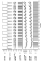
- FIG. 6 is a diagram showing an example of operation confirmation results when one synapse element circuit, one weight adjustment circuit, and one LIF neuron circuit are connected according to the present embodiment.
- a plurality of graphs shown in FIG. 6 show time variations of each value of weight setting, excitatory pulse, intraneuronal integration terminal, neuron output pulse, intrasynaptic integration output, integration result readout, and synapse output signal.
- the operation confirmation result shown in FIG. 6 only the excitatory pulse is input to the LIF neuron circuit 3, and the inhibitory pulse is not input.
- the weight setting indicates duty ratio setting data for the weight adjustment circuit 4 .
- the value of the signal that instructs the multiplexer M4 (FIG. 3) provided in the weight adjustment circuit 4 to select which of the plurality of delay elements forming the delay line D42 as the delay element for extracting the pulse signal is set to: show.
- the excitatory pulse indicates the value of the input pulse signal IP4 input to the input terminal IN4 provided in the weight adjustment circuit 4.
- FIG. An excitatory pulse is a pulse signal generated with a constant period, amplitude and duty ratio.
- the intra-neuron integration terminal indicates the value of the voltage V3 of the nodes provided in the LIF neuron circuit 3 (connection point J31, connection point J32, and connection point J33).
- the value of node voltage V3 is equal to the value of the voltage on capacitor C3 as described above.
- the neuron output pulse indicates the value of the output pulse signal OP3 output from the output terminal OUT3 provided in the LIF neuron circuit 3.
- the intra-synapse integration output indicates the value of the voltage V2 at the nodes provided in the synapse element circuit 2 (connection point J21, connection point J22, and connection point J23).
- the value of node voltage V2 is equal to the value of the voltage on capacitor C2 as described above.
- the integration result read indicates the value of the signal output from the output terminal OUT21 provided in the synapse element circuit 2.
- FIG. The synapse output signal indicates the value of the output pulse signal OP2 output from the output terminal OUT22 provided in the synapse element circuit 2.
- the synapse element circuit 2 functions as an LIF element from the time change of the intra-synapse integration output or the integration result readout.
- the average power consumption in the LIF neuron circuit 3 was 2.5 nW (nanowatts).
- the average power consumption in the synapse element circuit 2 was 3.0 nW.
- FIG. 7 is a diagram showing an example of operation confirmation results when one synapse element circuit, one weight adjustment circuit, and one LIF neuron circuit according to the present embodiment are connected.
- a plurality of graphs shown in FIG. 7 show temporal changes in each value of an excitatory pulse, an inhibitory pulse, an intra-synaptic integration output, an integration result readout, a synaptic output signal, an intra-neuron integration terminal, and a neuron output pulse.
- the LIF neuron circuit 3 receives an excitatory pulse and an inhibitory pulse.
- the excitatory pulse indicates the value of the input pulse signal IP31 input to the input terminal IN4 provided in the weight adjustment circuit 4.
- FIG. An excitatory pulse is a pulse signal generated with a constant period, amplitude and duty ratio.
- the inhibitory pulse indicates the value of the input pulse signal IP32 input to the input terminal IN32 provided in the weight adjustment circuit 4.
- FIG. An inhibitory pulse is a pulse signal generated with a constant period, amplitude, and duty ratio.
- the neuron output pulse is always low during the period when the inhibitory pulse is input.
- the pulse interval of the neuron output pulse is short in the period in which the pulse interval of the excitatory pulse is short. That is, as described above, in the LIF neuron circuit 3, the output frequency of the output pulse signal OP3 can be increased or decreased by the input pulse signal IP31, which is an excitatory pulse, or the input pulse signal IP32, which is an inhibitory pulse.
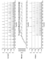
- FIG. 8 is a diagram showing an example of the operation check result of the spiking NN according to this embodiment.
- the spiking NN is composed of four module circuits 1, for example.
- a plurality of graphs shown in FIG. 8 show temporal changes in values of spike output, integration output, and VCO (Voltage-controlled oscillator) output.
- a plurality of graphs shown in FIG. 8 show respective values of the spike output, integration output, and VCO output for each of the four module circuits 1.
- FIG. 8 is a diagram showing an example of the operation check result of the spiking NN according to this embodiment.
- the spiking NN is composed of four module circuits 1, for example.
- a plurality of graphs shown in FIG. 8 show temporal changes in values of spike output, integration output, and VCO (Voltage-controlled oscillator) output.
- a plurality of graphs shown in FIG. 8 show respective values of the spike output, integration output, and VCO output for each of the four module circuits 1.
- the spike output indicates the value of the output pulse signal OP3 output from the output terminal OUT3 provided in the LIF neuron circuit 3.
- FIG. The integrated output indicates the value of the voltage V2 at the nodes (connection point J21, connection point J22, and connection point J23) provided in the synapse element circuit 2.
- the VCO output indicates the value of the output pulse signal OP2 output from the output terminal OUT22 provided in the synapse element circuit 2.
- FIG. 9 is a diagram showing an example of temporal changes in synapse output signals according to the present embodiment.
- the synapse output signal indicates the value of the output pulse signal OP2 output from the output terminal OUT21 provided in the synapse element circuit 2.
- FIG. 9 is a diagram showing an example of temporal changes in synapse output signals according to the present embodiment.
- the synapse output signal indicates the value of the output pulse signal OP2 output from the output terminal OUT21 provided in the synapse element circuit 2.
- the teacher signal is shown together with the synapse output signal.
- the teacher signal is a signal for learning that makes the value of the synapse output signal close to the value of the teacher signal.
- the teacher signal is input during the period from the time indicated as "RLS on” to the time indicated as "off” in FIG.
- the graph of the synapse output signal almost overlaps the graph of the teacher signal during the period when the teacher signal is being input.
- the graph of the synapse output signal shows the same temporal change as the period during which the teacher signal is input in the period after the input of the teacher signal (the period after the time indicated as "off"). That is, the graph of the synapse output signal changes with the teacher signal so as to change over time in the same way as the graph of the teacher signal. In other words, it can be seen that learning can be realized by the spiking NN composed of the module circuit 1.
- FIG. 10 is a diagram showing an example of temporal changes in neuron voltage according to this embodiment.
- the neuron voltage indicates the value of the voltage V3 of the nodes (connection point J31, connection point J32, and connection point J33) provided in the LIF neuron circuit 3, similar to the intra-neuron integration terminals (FIGS. 6 and 7) described above. .
- FIG. 11 is a diagram showing an example of temporal changes in synaptic currents according to this embodiment.
- the synapse current indicates the value of the voltage V2 at the nodes (connection point J21, connection point J22, and connection point J23) provided in the synapse element circuit 2, similar to the above-described intrasynaptic integral output (FIGS. 6 and 7). .
- the module circuit 1 includes a first block circuit (the synapse element circuit 2 in the present embodiment) and a second block circuit (the weight adjustment circuit 4 in the present embodiment). , provided.
- the first block circuit (synapse element circuit 2 in this embodiment) includes a first input terminal (input terminal IN21 in this embodiment), a holding section (capacitor C2 in this embodiment), an oscillation section (this In the embodiment, it includes a ring oscillator O2) and a first output terminal (output terminal OUT22 in the embodiment).
- the input pulse signal IP1 is input to the first input terminal (input terminal IN21 in this embodiment).
- the holding unit holds the average value of the input pulse signal IP1 for a predetermined period according to the interval of the input pulse signal IP1 and the width of the input pulse signal IP1.
- the oscillator (ring oscillator O2 in this embodiment) generates the output pulse signal OP2 at a frequency corresponding to the average value.
- the first output terminal (output terminal OUT22 in this embodiment) outputs an output pulse signal OP2.
- the second block circuit (weight adjustment circuit 4 in this embodiment) includes a second input terminal (input terminal IN4 in this embodiment) and a duty ratio adjuster (inverter D41, delay line D42, and multiplexer M4), and a second output terminal (output terminal OUT4 in this embodiment).
- the second input terminal receives the output pulse signal OP2 output from the first block circuit (synapse element circuit 2 in this embodiment).
- a duty ratio adjuster (in this embodiment, an inverter D41, a delay line D42, and a multiplexer M4) adjusts the duty ratio of the output pulse signal OP2.
- the second output terminal (output terminal OUT4 in this embodiment) outputs an output pulse signal (in this embodiment, It outputs an output pulse signal OP4).
- the output pulse signal can be output at a frequency corresponding to the time domain information such as the interval of the input pulse signal and the width of the pulse signal. realizable.
- the module circuit 1 according to the present embodiment relates to a low power consumption integrated circuit mounting system for neuron elements used in neural networks and the like.
- the module circuit 1 according to the present embodiment does not use voltage or current as information, but uses time-domain information such as the period and pulse width of binary pulse signals of low and high. Enables heat generation and high integration.
- the module circuit 1 according to the present embodiment can operate with extremely low power consumption because it operates mainly by utilizing the leak current flowing through the transistor in the off state.
- the module circuit 1 according to the present embodiment can operate with low power consumption, does not require a large capacity, and can realize a time constant in milliseconds with a relatively small area.
- the module circuit 1 adjusts the transition time between binary voltages of 0 or 1 without precisely controlling analog quantities that are sensitive to noise and the like. do. Therefore, it is easy to implement even in a low-voltage process technology, has a high affinity for advanced processes, and has the advantage of being able to increase the degree of integration.
- the enlarged area R2 is an enlarged area of the rectangular area R1 of the semiconductor chip.
- the enlarged region R2 has a long side length of 70 ⁇ m and a short side length of 30 ⁇ m.
- the area of the semiconductor chip of the LIF neuron circuit is 127 mm 2 .
- the area of the semiconductor chip of the synapse element circuit is 231 mm 2 .
- the area of the semiconductor chip of the weight adjustment circuit is 525 mm 2 .
- the configuration of the synapse element circuit 20 is the same as the configuration of the synapse element circuit 2 (FIG. 2) according to the embodiment described above.
- the configuration of the weight adjustment circuit 40 is the same as the configuration of the weight adjustment circuit 4 (FIG. 3) according to the embodiment described above.
- the configuration of the LIF neuron circuit 30 is the same as the configuration of the LIF neuron circuit 3 (FIG. 4) according to the embodiment described above. Therefore, in the examples described below, the respective symbols used in the above-described embodiments may be used for description.
- FIG. 13 is a diagram showing an example of the configuration of the module circuit 10a according to this embodiment.
- the module circuit 10 a includes a pulse generator 50 , a weight adjustment circuit 40 and a LIF neuron circuit 30 .
- the pulse generator 50, the weight adjustment circuit 40, and the LIF neuron circuit 30 are connected in series in this order and provided in the module circuit 10a.
- the pulse generator 50 generates a rectangular wave of 100 Hz as the input pulse signal IP4.
- An input pulse signal IP4 generated by the pulse generator 50 is input to the input terminal IN4 of the weight adjustment circuit 40.
- FIG. When the input pulse signal IP4 is input to the input terminal IN4, the output pulse signal OP4 is output from the output terminal OUT4 of the weight adjustment circuit 40.
- FIG. An output pulse signal OP4 output from the weight adjustment circuit 40 is input to the input terminal IN31 of the LIF neuron circuit 30.
- FIG. A spike signal V spike is output from an output terminal OUT3 of the LIF neuron circuit 30 as an output pulse signal OP3.
- FIG. 14 shows the waveform of the spike signal V spike output from the module circuit 10a as the operation measurement result of the module circuit 10a.
- 14(A), 14(B), 14(C), and 14(D) the weight values for adjusting the pulse width of the output pulse signal OP4 by the weight adjusting circuit 40 are 1 and 1, respectively.
- 2 shows the waveform of the spike signal V spike for 2, 4, and 8; As shown in FIG. 14, it was confirmed that the larger the weight, the shorter the spike period of the spike signal V spike .
- FIG. 15 is a diagram showing an example of the configuration of the module circuit 10b according to this embodiment.
- the module circuit 10 b includes a pulse generator 51 , a pulse generator 52 , a weight adjustment circuit 41 , a weight adjustment circuit 42 and a LIF neuron circuit 30 .
- the pulse generator 51 and weight adjustment circuit 41 are connected in series in this order.
- the pulse generator 52 and weight adjustment circuit 42 are connected in series in this order.
- a series-connected pulse generator 51 and weight adjustment circuit 41 and a series-connected pulse generator 52 and weight adjustment circuit 42 are connected in parallel to the LIF neuron circuit 30 .
- each of the weight adjustment circuit 41 and the weight adjustment circuit 42 is the same as the configuration of the weight adjustment circuit 40 .
- the configuration of each of the pulse generator 51 and the pulse generator 52 is the same as that of the pulse generator 50 .
- An input pulse signal IP4 which is a rectangular wave of 100 Hz generated by the pulse generator 51, is input to the input terminal IN4 of the weight adjustment circuit 41, and output from the output terminal OUT4 of the weight adjustment circuit 41 as an output pulse signal OP4.
- the input pulse signal IP4 which is a rectangular wave of 100 Hz generated by the pulse generator 52, is input to the input terminal IN4 of the weight adjustment circuit 42, and is output from the output terminal OUT4 of the weight adjustment circuit 42 as the output pulse signal OP4.
- An output pulse signal OP4 output from the weight adjustment circuit 41 is input to an input terminal IN31 of the LIF neuron circuit 30 as an input pulse signal IP31, which is an excitatory pulse.
- the output pulse signal OP4 output from the weight adjustment circuit 42 is input to the input terminal IN32 of the LIF neuron circuit 30 as the input pulse signal IP32, which is an inhibitory pulse.
- a spike signal V spike is output from an output terminal OUT3 of the LIF neuron circuit 30 as an output pulse signal OP3.
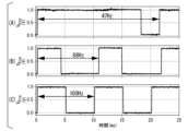
- FIG. 16 shows the waveform of the spike signal V spike output from the module circuit 10b as the operation measurement result of the module circuit 10b.
- FIG. 16A shows the waveform of the spike signal V spike when no signal is input to the input terminal IN31 and an inhibitory pulse (input pulse signal IP32) is input to the input terminal IN32.
- FIG. 16B shows the waveform of the spike signal V spike when no signal is input to either the input terminal IN31 or the input terminal IN32.
- FIG. 16C shows the waveform of the spike signal V spike when an excitatory pulse (input pulse signal IP31) is input to the input terminal IN31 and no signal is input to the input terminal IN32. As shown in FIG.
- the LIF neuron circuit 30 periodically outputs the spike signal V spike to the output terminal OUT3 even if no signal is input.
- the period of the spike signal V spike becomes longer.
- FIG. 16(C) when an excitatory pulse is input from the input terminal IN31, the cycle of the spike signal V spike is shortened.
- FIG. 17 is a diagram showing an example of the configuration of the module circuit 10c according to this embodiment. Comparing the configuration of the module circuit 10c and the configuration of the module circuit 10b (FIG. 15) according to the second embodiment, the synapse element circuit 20 is different. In the module circuit 10c, the LIF neuron circuit 30 and the synapse element circuit 20 are connected in series.
- a spike signal V spike output from the output terminal OUT3 of the LIF neuron circuit 30 is input to the input terminal IN22 of the synapse element circuit 20 .
- the pulse signal V ring generated by the ring oscillator O2 is output as the output pulse signal OP2.
- FIG. 18 shows the waveform of the pulse signal V ring output from the module circuit 10c as the operation measurement result of the module circuit 10c.
- FIG. 18A shows the waveform of the pulse signal V ring when no signal is input to the input terminal IN31 and an inhibitory pulse (input pulse signal IP32) is input to the input terminal IN32.
- FIG. 16B shows the waveform of the pulse signal Vring when no signal is input to either the input terminal IN31 or the input terminal IN32.
- FIG. 16(C) shows the waveform of the pulse signal Vring when an excitatory pulse (input pulse signal IP31) is input to the input terminal IN31 and no signal is input to the input terminal IN32. As shown in FIG.
- the synapse element circuit 20 periodically outputs a square wave as the pulse signal V ring in response to the spike signal V spike output from the LIF neuron circuit 30 .
- the frequency of the rectangular wave is reduced.
- the frequency of the rectangular wave increases.
- FIG. 19 is a diagram showing an example of the configuration of the module circuit 10d according to this embodiment.
- the module circuit 10 d includes a pulse generator 50 , a weight adjustment circuit 40 and a synapse element circuit 20 .
- the pulse generator 50, the weight adjustment circuit 40, and the synapse element circuit 20 are connected in series in this order and provided in the module circuit 10d.
- the pulse generator 50 generates a rectangular wave of 10 Hz as the input pulse signal IP4.
- An input pulse signal IP4 generated by the pulse generator 50 is input to the input terminal IN4 of the weight adjustment circuit 40.
- FIG. When the input pulse signal IP4 is input to the input terminal IN4, the output pulse signal OP4 is output from the output terminal OUT4 of the weight adjustment circuit 40.
- FIG. The output pulse signal OP4 output from the weight adjustment circuit 40 is input to the input terminal IN22 of the synapse element circuit 20.
- the output terminal OUT22 of the synapse element circuit 20 outputs the pulse signal V ring .
- FIG. 20 shows the waveform of the synapse potential signal V SYN and the waveform of the pulse signal V ring output from the module circuit 10d as the operation measurement results of the module circuit 10d.
- FIG. 20A shows the waveform of the synaptic potential signal V SYN .
- FIG. 20B shows the waveform of the pulse signal Vring .
- the pulse signal V ring is output as a rectangular wave whose frequency is modulated according to the voltage of the synapse potential signal V SYN .
- the synapse potential signal V SYN increases in response to the input to the input terminal IN22, the frequency of the pulse signal V ring increases.
- the synapse potential signal V SYN decreases and the frequency of the pulse signal V ring decreases.
- module circuit 2 synapse element circuit 4 weight adjustment circuit IN2 input terminal C2 capacitor O2 ring oscillator OUT22 output terminal IN4 input terminal D41 inverter D42 delay line M4...multiplexer, OUT4...output terminal, IP1...input pulse signal, OP2, OP4...output pulse signal
Landscapes
- Engineering & Computer Science (AREA)
- Physics & Mathematics (AREA)
- Theoretical Computer Science (AREA)
- Health & Medical Sciences (AREA)
- Biomedical Technology (AREA)
- Mathematical Physics (AREA)
- Life Sciences & Earth Sciences (AREA)
- Biophysics (AREA)
- General Physics & Mathematics (AREA)
- General Health & Medical Sciences (AREA)
- Software Systems (AREA)
- Molecular Biology (AREA)
- Evolutionary Computation (AREA)
- Computing Systems (AREA)
- General Engineering & Computer Science (AREA)
- Data Mining & Analysis (AREA)
- Computational Linguistics (AREA)
- Artificial Intelligence (AREA)
- Neurology (AREA)
- Computer Hardware Design (AREA)
- Neurosurgery (AREA)
- Physiology (AREA)
- Nonlinear Science (AREA)
- Electronic Switches (AREA)
- Logic Circuits (AREA)
Priority Applications (2)
| Application Number | Priority Date | Filing Date | Title |
|---|---|---|---|
| US18/715,699 US12525968B2 (en) | 2021-12-07 | 2022-12-05 | Module circuit and reservoir circuit |
| JP2023566302A JP7659852B2 (ja) | 2021-12-07 | 2022-12-05 | モジュール回路、及びレザバー回路 |
Applications Claiming Priority (2)
| Application Number | Priority Date | Filing Date | Title |
|---|---|---|---|
| JP2021-198579 | 2021-12-07 | ||
| JP2021198579 | 2021-12-07 |
Publications (1)
| Publication Number | Publication Date |
|---|---|
| WO2023106249A1 true WO2023106249A1 (ja) | 2023-06-15 |
Family
ID=86730344
Family Applications (1)
| Application Number | Title | Priority Date | Filing Date |
|---|---|---|---|
| PCT/JP2022/044655 Ceased WO2023106249A1 (ja) | 2021-12-07 | 2022-12-05 | モジュール回路、及びレザバー回路 |
Country Status (3)
| Country | Link |
|---|---|
| US (1) | US12525968B2 (https=) |
| JP (1) | JP7659852B2 (https=) |
| WO (1) | WO2023106249A1 (https=) |
Cited By (1)
| Publication number | Priority date | Publication date | Assignee | Title |
|---|---|---|---|---|
| WO2025239025A1 (ja) * | 2024-05-17 | 2025-11-20 | ソニーセミコンダクタソリューションズ株式会社 | 電子回路 |
Citations (2)
| Publication number | Priority date | Publication date | Assignee | Title |
|---|---|---|---|---|
| JP2005267105A (ja) * | 2004-03-17 | 2005-09-29 | Canon Inc | 並列パルス信号処理装置、パターン認識装置、及び画像入力装置 |
| US20180211165A1 (en) * | 2017-01-25 | 2018-07-26 | Electronics And Telecommunications Research Institute | Neuromorphic arithmetic device |
Family Cites Families (5)
| Publication number | Priority date | Publication date | Assignee | Title |
|---|---|---|---|---|
| EP0390226A1 (en) * | 1984-07-31 | 1990-10-03 | Yamaha Corporation | Jitter absorption circuit |
| US6819190B2 (en) * | 2002-12-10 | 2004-11-16 | Intersil Americas Inc. | Robust fractional clock-based pulse generator for digital pulse width modulator |
| US7271754B2 (en) * | 2005-02-22 | 2007-09-18 | The Regents Of The University Of Colorado, A Body Corporate | Digital pulse-width modulator |
| US10396807B1 (en) * | 2016-02-08 | 2019-08-27 | Auburn University | Multi-ring coupled ring oscillator with improved phase noise |
| US20180191356A1 (en) * | 2017-01-03 | 2018-07-05 | Allegro Microsystems, Llc | Control circuit |
-
2022
- 2022-12-05 US US18/715,699 patent/US12525968B2/en active Active
- 2022-12-05 WO PCT/JP2022/044655 patent/WO2023106249A1/ja not_active Ceased
- 2022-12-05 JP JP2023566302A patent/JP7659852B2/ja active Active
Patent Citations (2)
| Publication number | Priority date | Publication date | Assignee | Title |
|---|---|---|---|---|
| JP2005267105A (ja) * | 2004-03-17 | 2005-09-29 | Canon Inc | 並列パルス信号処理装置、パターン認識装置、及び画像入力装置 |
| US20180211165A1 (en) * | 2017-01-25 | 2018-07-26 | Electronics And Telecommunications Research Institute | Neuromorphic arithmetic device |
Non-Patent Citations (1)
| Title |
|---|
| HANAA MOHSIN AL-ABBOODY, HAIDER. J. ABD, ALAA. H. ABDULLA, MOHAMMED TAIH GATTE, MUSTAFA ISMAEL, HAYDER HUSSEIN KADHUM: "Review Paper: Background and Evolution of Spiking Neural Networks", IAETSD JOURNAL FOR ADVANCED RESEARCH IN APPLIED SCIENCES, vol. 8, no. 7, 1 July 2021 (2021-07-01), pages 9 - 16, XP009547057, ISSN: 2394-8442 * |
Cited By (1)
| Publication number | Priority date | Publication date | Assignee | Title |
|---|---|---|---|---|
| WO2025239025A1 (ja) * | 2024-05-17 | 2025-11-20 | ソニーセミコンダクタソリューションズ株式会社 | 電子回路 |
Also Published As
| Publication number | Publication date |
|---|---|
| JPWO2023106249A1 (https=) | 2023-06-15 |
| US20250030412A1 (en) | 2025-01-23 |
| JP7659852B2 (ja) | 2025-04-10 |
| US12525968B2 (en) | 2026-01-13 |
Similar Documents
| Publication | Publication Date | Title |
|---|---|---|
| KR102230784B1 (ko) | Stdp 동작을 위한 시냅스 회로 및 시냅스 회로를 포함하는 뉴로모픽 시스템 | |
| US7310013B2 (en) | Method, apparatus, and system for low voltage temperature sensing | |
| US20090315530A1 (en) | Pulse controlled soft start scheme for buck converter | |
| US11444605B2 (en) | Spike generation circuit, information processing circuit, power conversion circuit, detector, and electronic circuit | |
| US7425857B2 (en) | Time-delay circuit | |
| TW200825654A (en) | Charge pump circuit | |
| US6411554B1 (en) | High voltage switch circuit having transistors and semiconductor memory device provided with the same | |
| US11551070B2 (en) | Artificial neuromorphic circuit and operation method | |
| US6876244B1 (en) | Differential charge pump | |
| WO2023106249A1 (ja) | モジュール回路、及びレザバー回路 | |
| US9081402B2 (en) | Semiconductor device having a complementary field effect transistor | |
| KR0146076B1 (ko) | 반도체 소자의 기판 전압 레규레이터 장치 | |
| US20050258911A1 (en) | Ring oscillation circuit | |
| US10719094B2 (en) | Internal voltage generation circuits | |
| US20050001667A1 (en) | Delay circuit with more-responsively adapting delay time | |
| CN112994659B (zh) | 弛豫振荡器和控制弛豫振荡器的方法 | |
| KR20220065299A (ko) | 플래시 메모리 기반의 스파이크 레귤레이터를 포함하는 뉴로모픽 회로 | |
| JPH08330921A (ja) | 可変遅延回路 | |
| JP2019161379A (ja) | 発振回路 | |
| US20260080233A1 (en) | Neural network device and signal processing method | |
| TWI855722B (zh) | 倍頻器以及責任週期調整方法 | |
| TWI795884B (zh) | 測量工作週期之裝置及補償電路 | |
| CN113258878B (zh) | 振荡器 | |
| JP2023142121A (ja) | スイッチングレギュレータ制御回路 | |
| US20240297646A1 (en) | Spiking Neuron Circuit System and Spiking Neuron Circuit |
Legal Events
| Date | Code | Title | Description |
|---|---|---|---|
| 121 | Ep: the epo has been informed by wipo that ep was designated in this application |
Ref document number: 22904178 Country of ref document: EP Kind code of ref document: A1 |
|
| ENP | Entry into the national phase |
Ref document number: 2023566302 Country of ref document: JP Kind code of ref document: A |
|
| WWE | Wipo information: entry into national phase |
Ref document number: 18715699 Country of ref document: US |
|
| NENP | Non-entry into the national phase |
Ref country code: DE |
|
| 122 | Ep: pct application non-entry in european phase |
Ref document number: 22904178 Country of ref document: EP Kind code of ref document: A1 |
|
| WWG | Wipo information: grant in national office |
Ref document number: 18715699 Country of ref document: US |