WO2023106153A1 - Film conducteur, électrode et procédé de fabrication de film conducteur - Google Patents
Film conducteur, électrode et procédé de fabrication de film conducteur Download PDFInfo
- Publication number
- WO2023106153A1 WO2023106153A1 PCT/JP2022/043779 JP2022043779W WO2023106153A1 WO 2023106153 A1 WO2023106153 A1 WO 2023106153A1 JP 2022043779 W JP2022043779 W JP 2022043779W WO 2023106153 A1 WO2023106153 A1 WO 2023106153A1
- Authority
- WO
- WIPO (PCT)
- Prior art keywords
- conductive film
- mxene
- less
- atom
- particles
- Prior art date
Links
- 238000004519 manufacturing process Methods 0.000 title claims description 34
- 238000000034 method Methods 0.000 title description 19
- 239000010936 titanium Substances 0.000 claims abstract description 66
- 239000002245 particle Substances 0.000 claims abstract description 56
- 239000000463 material Substances 0.000 claims abstract description 55
- 229910052719 titanium Inorganic materials 0.000 claims abstract description 40
- RTAQQCXQSZGOHL-UHFFFAOYSA-N Titanium Chemical compound [Ti] RTAQQCXQSZGOHL-UHFFFAOYSA-N 0.000 claims abstract description 37
- GWEVSGVZZGPLCZ-UHFFFAOYSA-N Titan oxide Chemical compound O=[Ti]=O GWEVSGVZZGPLCZ-UHFFFAOYSA-N 0.000 claims abstract description 28
- OGIDPMRJRNCKJF-UHFFFAOYSA-N titanium oxide Inorganic materials [Ti]=O OGIDPMRJRNCKJF-UHFFFAOYSA-N 0.000 claims abstract description 28
- 238000004833 X-ray photoelectron spectroscopy Methods 0.000 claims abstract description 18
- 229910052751 metal Inorganic materials 0.000 claims abstract description 15
- 239000002184 metal Substances 0.000 claims abstract description 15
- 229910052799 carbon Inorganic materials 0.000 claims abstract description 13
- 238000001228 spectrum Methods 0.000 claims abstract description 13
- 238000012986 modification Methods 0.000 claims abstract description 10
- 230000004048 modification Effects 0.000 claims abstract description 10
- 229910052757 nitrogen Inorganic materials 0.000 claims abstract description 10
- 125000004433 nitrogen atom Chemical group N* 0.000 claims abstract description 10
- 125000001309 chloro group Chemical group Cl* 0.000 claims abstract description 9
- 229910052731 fluorine Inorganic materials 0.000 claims abstract description 9
- 125000001153 fluoro group Chemical group F* 0.000 claims abstract description 9
- 125000004435 hydrogen atom Chemical group [H]* 0.000 claims abstract description 9
- 125000002887 hydroxy group Chemical group [H]O* 0.000 claims abstract description 9
- 125000004430 oxygen atom Chemical group O* 0.000 claims abstract description 9
- 229910052801 chlorine Inorganic materials 0.000 claims abstract description 8
- 125000004432 carbon atom Chemical group C* 0.000 claims abstract 4
- 230000032683 aging Effects 0.000 claims description 26
- 239000002243 precursor Substances 0.000 claims description 23
- 239000006185 dispersion Substances 0.000 claims description 17
- 239000010410 layer Substances 0.000 description 74
- 239000012528 membrane Substances 0.000 description 21
- 238000005530 etching Methods 0.000 description 20
- 239000007788 liquid Substances 0.000 description 19
- 229910021645 metal ion Inorganic materials 0.000 description 18
- 239000002356 single layer Substances 0.000 description 18
- 239000002002 slurry Substances 0.000 description 17
- 238000009830 intercalation Methods 0.000 description 15
- 230000002687 intercalation Effects 0.000 description 15
- 239000006228 supernatant Substances 0.000 description 14
- 125000004429 atom Chemical group 0.000 description 13
- 239000000758 substrate Substances 0.000 description 13
- 230000032798 delamination Effects 0.000 description 12
- 230000003647 oxidation Effects 0.000 description 12
- 238000007254 oxidation reaction Methods 0.000 description 12
- 150000002736 metal compounds Chemical class 0.000 description 11
- 239000002609 medium Substances 0.000 description 10
- 238000001035 drying Methods 0.000 description 9
- 239000000843 powder Substances 0.000 description 9
- XLYOFNOQVPJJNP-UHFFFAOYSA-N water Substances O XLYOFNOQVPJJNP-UHFFFAOYSA-N 0.000 description 9
- 239000002585 base Substances 0.000 description 8
- HBBGRARXTFLTSG-UHFFFAOYSA-N Lithium ion Chemical compound [Li+] HBBGRARXTFLTSG-UHFFFAOYSA-N 0.000 description 7
- 239000003990 capacitor Substances 0.000 description 7
- 239000004927 clay Substances 0.000 description 7
- 229910001416 lithium ion Inorganic materials 0.000 description 7
- 238000005259 measurement Methods 0.000 description 7
- 239000013078 crystal Substances 0.000 description 6
- 239000000243 solution Substances 0.000 description 6
- 150000001721 carbon Chemical group 0.000 description 5
- 239000002612 dispersion medium Substances 0.000 description 5
- 150000002500 ions Chemical class 0.000 description 5
- 239000000203 mixture Substances 0.000 description 5
- 239000011368 organic material Substances 0.000 description 5
- 239000011148 porous material Substances 0.000 description 5
- 238000002360 preparation method Methods 0.000 description 5
- 239000000047 product Substances 0.000 description 5
- 229910052720 vanadium Inorganic materials 0.000 description 5
- 239000011230 binding agent Substances 0.000 description 4
- 238000000576 coating method Methods 0.000 description 4
- 230000007423 decrease Effects 0.000 description 4
- 239000003792 electrolyte Substances 0.000 description 4
- KWGKDLIKAYFUFQ-UHFFFAOYSA-M lithium chloride Chemical compound [Li+].[Cl-] KWGKDLIKAYFUFQ-UHFFFAOYSA-M 0.000 description 4
- BASFCYQUMIYNBI-UHFFFAOYSA-N platinum Chemical compound [Pt] BASFCYQUMIYNBI-UHFFFAOYSA-N 0.000 description 4
- 239000002244 precipitate Substances 0.000 description 4
- 230000008569 process Effects 0.000 description 4
- 239000007921 spray Substances 0.000 description 4
- 238000005507 spraying Methods 0.000 description 4
- 239000000126 substance Substances 0.000 description 4
- 238000005406 washing Methods 0.000 description 4
- QTBSBXVTEAMEQO-UHFFFAOYSA-N Acetic acid Chemical compound CC(O)=O QTBSBXVTEAMEQO-UHFFFAOYSA-N 0.000 description 3
- OKTJSMMVPCPJKN-UHFFFAOYSA-N Carbon Chemical compound [C] OKTJSMMVPCPJKN-UHFFFAOYSA-N 0.000 description 3
- LFQSCWFLJHTTHZ-UHFFFAOYSA-N Ethanol Chemical compound CCO LFQSCWFLJHTTHZ-UHFFFAOYSA-N 0.000 description 3
- LYCAIKOWRPUZTN-UHFFFAOYSA-N Ethylene glycol Chemical compound OCCO LYCAIKOWRPUZTN-UHFFFAOYSA-N 0.000 description 3
- OKKJLVBELUTLKV-UHFFFAOYSA-N Methanol Chemical compound OC OKKJLVBELUTLKV-UHFFFAOYSA-N 0.000 description 3
- ZMXDDKWLCZADIW-UHFFFAOYSA-N N,N-Dimethylformamide Chemical compound CN(C)C=O ZMXDDKWLCZADIW-UHFFFAOYSA-N 0.000 description 3
- 241000209094 Oryza Species 0.000 description 3
- 235000007164 Oryza sativa Nutrition 0.000 description 3
- 239000012736 aqueous medium Substances 0.000 description 3
- 238000005119 centrifugation Methods 0.000 description 3
- 239000011248 coating agent Substances 0.000 description 3
- 150000001875 compounds Chemical class 0.000 description 3
- 230000000694 effects Effects 0.000 description 3
- -1 flakes Substances 0.000 description 3
- 230000002431 foraging effect Effects 0.000 description 3
- 229910052750 molybdenum Inorganic materials 0.000 description 3
- 229910052758 niobium Inorganic materials 0.000 description 3
- 230000001590 oxidative effect Effects 0.000 description 3
- 239000011347 resin Substances 0.000 description 3
- 229920005989 resin Polymers 0.000 description 3
- 235000009566 rice Nutrition 0.000 description 3
- 238000000926 separation method Methods 0.000 description 3
- 239000007787 solid Substances 0.000 description 3
- 238000003756 stirring Methods 0.000 description 3
- 229920000298 Cellophane Polymers 0.000 description 2
- IAZDPXIOMUYVGZ-UHFFFAOYSA-N Dimethylsulphoxide Chemical compound CS(C)=O IAZDPXIOMUYVGZ-UHFFFAOYSA-N 0.000 description 2
- KRHYYFGTRYWZRS-UHFFFAOYSA-N Fluorane Chemical compound F KRHYYFGTRYWZRS-UHFFFAOYSA-N 0.000 description 2
- VEXZGXHMUGYJMC-UHFFFAOYSA-N Hydrochloric acid Chemical compound Cl VEXZGXHMUGYJMC-UHFFFAOYSA-N 0.000 description 2
- XEEYBQQBJWHFJM-UHFFFAOYSA-N Iron Chemical compound [Fe] XEEYBQQBJWHFJM-UHFFFAOYSA-N 0.000 description 2
- ATHHXGZTWNVVOU-UHFFFAOYSA-N N-methylformamide Chemical compound CNC=O ATHHXGZTWNVVOU-UHFFFAOYSA-N 0.000 description 2
- PXHVJJICTQNCMI-UHFFFAOYSA-N Nickel Chemical compound [Ni] PXHVJJICTQNCMI-UHFFFAOYSA-N 0.000 description 2
- 239000004433 Thermoplastic polyurethane Substances 0.000 description 2
- 229910009819 Ti3C2 Inorganic materials 0.000 description 2
- MCMNRKCIXSYSNV-UHFFFAOYSA-N Zirconium dioxide Chemical compound O=[Zr]=O MCMNRKCIXSYSNV-UHFFFAOYSA-N 0.000 description 2
- 239000002253 acid Substances 0.000 description 2
- 229910052782 aluminium Inorganic materials 0.000 description 2
- QVGXLLKOCUKJST-UHFFFAOYSA-N atomic oxygen Chemical compound [O] QVGXLLKOCUKJST-UHFFFAOYSA-N 0.000 description 2
- 238000000889 atomisation Methods 0.000 description 2
- 238000007664 blowing Methods 0.000 description 2
- 229910052804 chromium Inorganic materials 0.000 description 2
- 239000004020 conductor Substances 0.000 description 2
- 238000001514 detection method Methods 0.000 description 2
- 230000006866 deterioration Effects 0.000 description 2
- 238000010586 diagram Methods 0.000 description 2
- 238000002593 electrical impedance tomography Methods 0.000 description 2
- 238000002848 electrochemical method Methods 0.000 description 2
- 238000002567 electromyography Methods 0.000 description 2
- 238000001914 filtration Methods 0.000 description 2
- 239000012530 fluid Substances 0.000 description 2
- 229910052737 gold Inorganic materials 0.000 description 2
- 239000010931 gold Substances 0.000 description 2
- 229910010272 inorganic material Inorganic materials 0.000 description 2
- 239000011147 inorganic material Substances 0.000 description 2
- 150000008040 ionic compounds Chemical class 0.000 description 2
- PQXKHYXIUOZZFA-UHFFFAOYSA-M lithium fluoride Chemical compound [Li+].[F-] PQXKHYXIUOZZFA-UHFFFAOYSA-M 0.000 description 2
- 239000007769 metal material Substances 0.000 description 2
- 238000001000 micrograph Methods 0.000 description 2
- 239000011812 mixed powder Substances 0.000 description 2
- 230000001537 neural effect Effects 0.000 description 2
- 229910052760 oxygen Inorganic materials 0.000 description 2
- 239000001301 oxygen Substances 0.000 description 2
- 229910052697 platinum Inorganic materials 0.000 description 2
- 229920000139 polyethylene terephthalate Polymers 0.000 description 2
- 229920001721 polyimide Polymers 0.000 description 2
- 238000007639 printing Methods 0.000 description 2
- 230000001737 promoting effect Effects 0.000 description 2
- 238000010008 shearing Methods 0.000 description 2
- 229910052709 silver Inorganic materials 0.000 description 2
- 239000004332 silver Substances 0.000 description 2
- 229910001415 sodium ion Inorganic materials 0.000 description 2
- 238000000527 sonication Methods 0.000 description 2
- 230000003595 spectral effect Effects 0.000 description 2
- 238000000967 suction filtration Methods 0.000 description 2
- 239000002344 surface layer Substances 0.000 description 2
- 229920002803 thermoplastic polyurethane Polymers 0.000 description 2
- 150000003568 thioethers Chemical class 0.000 description 2
- 229910052718 tin Inorganic materials 0.000 description 2
- 239000011135 tin Substances 0.000 description 2
- 229920002799 BoPET Polymers 0.000 description 1
- RYGMFSIKBFXOCR-UHFFFAOYSA-N Copper Chemical compound [Cu] RYGMFSIKBFXOCR-UHFFFAOYSA-N 0.000 description 1
- JPVYNHNXODAKFH-UHFFFAOYSA-N Cu2+ Chemical compound [Cu+2] JPVYNHNXODAKFH-UHFFFAOYSA-N 0.000 description 1
- YCKRFDGAMUMZLT-UHFFFAOYSA-N Fluorine atom Chemical compound [F] YCKRFDGAMUMZLT-UHFFFAOYSA-N 0.000 description 1
- FYYHWMGAXLPEAU-UHFFFAOYSA-N Magnesium Chemical compound [Mg] FYYHWMGAXLPEAU-UHFFFAOYSA-N 0.000 description 1
- JLVVSXFLKOJNIY-UHFFFAOYSA-N Magnesium ion Chemical compound [Mg+2] JLVVSXFLKOJNIY-UHFFFAOYSA-N 0.000 description 1
- ZOKXTWBITQBERF-UHFFFAOYSA-N Molybdenum Chemical compound [Mo] ZOKXTWBITQBERF-UHFFFAOYSA-N 0.000 description 1
- SECXISVLQFMRJM-UHFFFAOYSA-N N-Methylpyrrolidone Chemical compound CN1CCCC1=O SECXISVLQFMRJM-UHFFFAOYSA-N 0.000 description 1
- 229910019142 PO4 Inorganic materials 0.000 description 1
- 239000004642 Polyimide Substances 0.000 description 1
- BQCADISMDOOEFD-UHFFFAOYSA-N Silver Chemical compound [Ag] BQCADISMDOOEFD-UHFFFAOYSA-N 0.000 description 1
- FKNQFGJONOIPTF-UHFFFAOYSA-N Sodium cation Chemical compound [Na+] FKNQFGJONOIPTF-UHFFFAOYSA-N 0.000 description 1
- ATJFFYVFTNAWJD-UHFFFAOYSA-N Tin Chemical compound [Sn] ATJFFYVFTNAWJD-UHFFFAOYSA-N 0.000 description 1
- HCHKCACWOHOZIP-UHFFFAOYSA-N Zinc Chemical compound [Zn] HCHKCACWOHOZIP-UHFFFAOYSA-N 0.000 description 1
- JDZCKJOXGCMJGS-UHFFFAOYSA-N [Li].[S] Chemical compound [Li].[S] JDZCKJOXGCMJGS-UHFFFAOYSA-N 0.000 description 1
- 230000005856 abnormality Effects 0.000 description 1
- 150000001242 acetic acid derivatives Chemical class 0.000 description 1
- 238000007605 air drying Methods 0.000 description 1
- 229910001413 alkali metal ion Inorganic materials 0.000 description 1
- XAGFODPZIPBFFR-UHFFFAOYSA-N aluminium Chemical compound [Al] XAGFODPZIPBFFR-UHFFFAOYSA-N 0.000 description 1
- 238000004458 analytical method Methods 0.000 description 1
- 238000010171 animal model Methods 0.000 description 1
- 239000007864 aqueous solution Substances 0.000 description 1
- 229910052785 arsenic Inorganic materials 0.000 description 1
- 230000000035 biogenic effect Effects 0.000 description 1
- 230000015572 biosynthetic process Effects 0.000 description 1
- 210000004556 brain Anatomy 0.000 description 1
- 229910052793 cadmium Inorganic materials 0.000 description 1
- 150000007942 carboxylates Chemical class 0.000 description 1
- 150000001768 cations Chemical class 0.000 description 1
- 239000000919 ceramic Substances 0.000 description 1
- 235000013339 cereals Nutrition 0.000 description 1
- 230000008859 change Effects 0.000 description 1
- 238000006243 chemical reaction Methods 0.000 description 1
- GTKRFUAGOKINCA-UHFFFAOYSA-M chlorosilver;silver Chemical compound [Ag].[Ag]Cl GTKRFUAGOKINCA-UHFFFAOYSA-M 0.000 description 1
- 238000004140 cleaning Methods 0.000 description 1
- 230000000052 comparative effect Effects 0.000 description 1
- 229920001940 conductive polymer Polymers 0.000 description 1
- 229910052802 copper Inorganic materials 0.000 description 1
- 239000010949 copper Substances 0.000 description 1
- 229910001431 copper ion Inorganic materials 0.000 description 1
- 230000001054 cortical effect Effects 0.000 description 1
- 238000007865 diluting Methods 0.000 description 1
- 238000010790 dilution Methods 0.000 description 1
- 239000012895 dilution Substances 0.000 description 1
- 238000003618 dip coating Methods 0.000 description 1
- 229920001971 elastomer Polymers 0.000 description 1
- 239000000806 elastomer Substances 0.000 description 1
- 239000007772 electrode material Substances 0.000 description 1
- 230000007831 electrophysiology Effects 0.000 description 1
- 238000002001 electrophysiology Methods 0.000 description 1
- 238000005516 engineering process Methods 0.000 description 1
- 238000011156 evaluation Methods 0.000 description 1
- 230000001747 exhibiting effect Effects 0.000 description 1
- 238000000605 extraction Methods 0.000 description 1
- 239000011737 fluorine Substances 0.000 description 1
- 239000011888 foil Substances 0.000 description 1
- 229910052733 gallium Inorganic materials 0.000 description 1
- 239000007789 gas Substances 0.000 description 1
- 229910052732 germanium Inorganic materials 0.000 description 1
- PCHJSUWPFVWCPO-UHFFFAOYSA-N gold Chemical compound [Au] PCHJSUWPFVWCPO-UHFFFAOYSA-N 0.000 description 1
- 229910052735 hafnium Inorganic materials 0.000 description 1
- 238000007602 hot air drying Methods 0.000 description 1
- DKAGJZJALZXOOV-UHFFFAOYSA-N hydrate;hydrochloride Chemical compound O.Cl DKAGJZJALZXOOV-UHFFFAOYSA-N 0.000 description 1
- 229920001477 hydrophilic polymer Polymers 0.000 description 1
- 229910052738 indium Inorganic materials 0.000 description 1
- 239000011229 interlayer Substances 0.000 description 1
- 150000004694 iodide salts Chemical class 0.000 description 1
- 229910052742 iron Inorganic materials 0.000 description 1
- 238000003475 lamination Methods 0.000 description 1
- 229910052745 lead Inorganic materials 0.000 description 1
- 229910052749 magnesium Inorganic materials 0.000 description 1
- 239000011777 magnesium Substances 0.000 description 1
- 229910001425 magnesium ion Inorganic materials 0.000 description 1
- 238000012423 maintenance Methods 0.000 description 1
- 229910052748 manganese Inorganic materials 0.000 description 1
- 238000013507 mapping Methods 0.000 description 1
- 230000007246 mechanism Effects 0.000 description 1
- 239000011259 mixed solution Substances 0.000 description 1
- 238000002156 mixing Methods 0.000 description 1
- 239000011733 molybdenum Substances 0.000 description 1
- 239000002086 nanomaterial Substances 0.000 description 1
- 239000002135 nanosheet Substances 0.000 description 1
- 230000002232 neuromuscular Effects 0.000 description 1
- 229910052759 nickel Inorganic materials 0.000 description 1
- 150000002823 nitrates Chemical class 0.000 description 1
- 239000012466 permeate Substances 0.000 description 1
- 235000021317 phosphate Nutrition 0.000 description 1
- 150000003013 phosphoric acid derivatives Chemical class 0.000 description 1
- 229910052698 phosphorus Inorganic materials 0.000 description 1
- 229920003223 poly(pyromellitimide-1,4-diphenyl ether) Polymers 0.000 description 1
- 229920000642 polymer Polymers 0.000 description 1
- 229910001414 potassium ion Inorganic materials 0.000 description 1
- 238000012545 processing Methods 0.000 description 1
- 230000009467 reduction Effects 0.000 description 1
- 238000011160 research Methods 0.000 description 1
- 150000003839 salts Chemical class 0.000 description 1
- 238000001878 scanning electron micrograph Methods 0.000 description 1
- 230000035945 sensitivity Effects 0.000 description 1
- 229910052710 silicon Inorganic materials 0.000 description 1
- 238000004528 spin coating Methods 0.000 description 1
- 230000000638 stimulation Effects 0.000 description 1
- 229910052717 sulfur Inorganic materials 0.000 description 1
- 150000003467 sulfuric acid derivatives Chemical class 0.000 description 1
- 239000000725 suspension Substances 0.000 description 1
- 229910052715 tantalum Inorganic materials 0.000 description 1
- 239000013076 target substance Substances 0.000 description 1
- 229910052716 thallium Inorganic materials 0.000 description 1
- WFKWXMTUELFFGS-UHFFFAOYSA-N tungsten Chemical compound [W] WFKWXMTUELFFGS-UHFFFAOYSA-N 0.000 description 1
- 229910052721 tungsten Inorganic materials 0.000 description 1
- 239000010937 tungsten Substances 0.000 description 1
- 238000001291 vacuum drying Methods 0.000 description 1
- GPPXJZIENCGNKB-UHFFFAOYSA-N vanadium Chemical compound [V]#[V] GPPXJZIENCGNKB-UHFFFAOYSA-N 0.000 description 1
- 239000011800 void material Substances 0.000 description 1
- 229910052725 zinc Inorganic materials 0.000 description 1
- 239000011701 zinc Substances 0.000 description 1
- 229910052726 zirconium Inorganic materials 0.000 description 1
Images

Classifications
-
- H—ELECTRICITY
- H01—ELECTRIC ELEMENTS
- H01B—CABLES; CONDUCTORS; INSULATORS; SELECTION OF MATERIALS FOR THEIR CONDUCTIVE, INSULATING OR DIELECTRIC PROPERTIES
- H01B1/00—Conductors or conductive bodies characterised by the conductive materials; Selection of materials as conductors
- H01B1/06—Conductors or conductive bodies characterised by the conductive materials; Selection of materials as conductors mainly consisting of other non-metallic substances
- H01B1/08—Conductors or conductive bodies characterised by the conductive materials; Selection of materials as conductors mainly consisting of other non-metallic substances oxides
-
- C—CHEMISTRY; METALLURGY
- C01—INORGANIC CHEMISTRY
- C01G—COMPOUNDS CONTAINING METALS NOT COVERED BY SUBCLASSES C01D OR C01F
- C01G23/00—Compounds of titanium
-
- H—ELECTRICITY
- H01—ELECTRIC ELEMENTS
- H01B—CABLES; CONDUCTORS; INSULATORS; SELECTION OF MATERIALS FOR THEIR CONDUCTIVE, INSULATING OR DIELECTRIC PROPERTIES
- H01B1/00—Conductors or conductive bodies characterised by the conductive materials; Selection of materials as conductors
- H01B1/20—Conductive material dispersed in non-conductive organic material
-
- H—ELECTRICITY
- H01—ELECTRIC ELEMENTS
- H01B—CABLES; CONDUCTORS; INSULATORS; SELECTION OF MATERIALS FOR THEIR CONDUCTIVE, INSULATING OR DIELECTRIC PROPERTIES
- H01B13/00—Apparatus or processes specially adapted for manufacturing conductors or cables
-
- H—ELECTRICITY
- H01—ELECTRIC ELEMENTS
- H01B—CABLES; CONDUCTORS; INSULATORS; SELECTION OF MATERIALS FOR THEIR CONDUCTIVE, INSULATING OR DIELECTRIC PROPERTIES
- H01B5/00—Non-insulated conductors or conductive bodies characterised by their form
-
- H—ELECTRICITY
- H01—ELECTRIC ELEMENTS
- H01G—CAPACITORS; CAPACITORS, RECTIFIERS, DETECTORS, SWITCHING DEVICES, LIGHT-SENSITIVE OR TEMPERATURE-SENSITIVE DEVICES OF THE ELECTROLYTIC TYPE
- H01G11/00—Hybrid capacitors, i.e. capacitors having different positive and negative electrodes; Electric double-layer [EDL] capacitors; Processes for the manufacture thereof or of parts thereof
- H01G11/22—Electrodes
- H01G11/30—Electrodes characterised by their material
- H01G11/32—Carbon-based
- H01G11/36—Nanostructures, e.g. nanofibres, nanotubes or fullerenes
-
- H—ELECTRICITY
- H01—ELECTRIC ELEMENTS
- H01G—CAPACITORS; CAPACITORS, RECTIFIERS, DETECTORS, SWITCHING DEVICES, LIGHT-SENSITIVE OR TEMPERATURE-SENSITIVE DEVICES OF THE ELECTROLYTIC TYPE
- H01G11/00—Hybrid capacitors, i.e. capacitors having different positive and negative electrodes; Electric double-layer [EDL] capacitors; Processes for the manufacture thereof or of parts thereof
- H01G11/22—Electrodes
- H01G11/30—Electrodes characterised by their material
- H01G11/32—Carbon-based
- H01G11/42—Powders or particles, e.g. composition thereof
-
- H—ELECTRICITY
- H01—ELECTRIC ELEMENTS
- H01G—CAPACITORS; CAPACITORS, RECTIFIERS, DETECTORS, SWITCHING DEVICES, LIGHT-SENSITIVE OR TEMPERATURE-SENSITIVE DEVICES OF THE ELECTROLYTIC TYPE
- H01G11/00—Hybrid capacitors, i.e. capacitors having different positive and negative electrodes; Electric double-layer [EDL] capacitors; Processes for the manufacture thereof or of parts thereof
- H01G11/22—Electrodes
- H01G11/30—Electrodes characterised by their material
- H01G11/46—Metal oxides
-
- H—ELECTRICITY
- H01—ELECTRIC ELEMENTS
- H01G—CAPACITORS; CAPACITORS, RECTIFIERS, DETECTORS, SWITCHING DEVICES, LIGHT-SENSITIVE OR TEMPERATURE-SENSITIVE DEVICES OF THE ELECTROLYTIC TYPE
- H01G11/00—Hybrid capacitors, i.e. capacitors having different positive and negative electrodes; Electric double-layer [EDL] capacitors; Processes for the manufacture thereof or of parts thereof
- H01G11/84—Processes for the manufacture of hybrid or EDL capacitors, or components thereof
- H01G11/86—Processes for the manufacture of hybrid or EDL capacitors, or components thereof specially adapted for electrodes
-
- H—ELECTRICITY
- H01—ELECTRIC ELEMENTS
- H01M—PROCESSES OR MEANS, e.g. BATTERIES, FOR THE DIRECT CONVERSION OF CHEMICAL ENERGY INTO ELECTRICAL ENERGY
- H01M4/00—Electrodes
- H01M4/02—Electrodes composed of, or comprising, active material
-
- H—ELECTRICITY
- H01—ELECTRIC ELEMENTS
- H01M—PROCESSES OR MEANS, e.g. BATTERIES, FOR THE DIRECT CONVERSION OF CHEMICAL ENERGY INTO ELECTRICAL ENERGY
- H01M4/00—Electrodes
- H01M4/02—Electrodes composed of, or comprising, active material
- H01M4/13—Electrodes for accumulators with non-aqueous electrolyte, e.g. for lithium-accumulators; Processes of manufacture thereof
-
- H—ELECTRICITY
- H01—ELECTRIC ELEMENTS
- H01M—PROCESSES OR MEANS, e.g. BATTERIES, FOR THE DIRECT CONVERSION OF CHEMICAL ENERGY INTO ELECTRICAL ENERGY
- H01M4/00—Electrodes
- H01M4/02—Electrodes composed of, or comprising, active material
- H01M4/62—Selection of inactive substances as ingredients for active masses, e.g. binders, fillers
Definitions
- the present disclosure relates to conductive films, electrodes, and methods of manufacturing conductive films.
- MXene has attracted attention as a new material.
- MXene is a type of so-called two-dimensional material, which is a layered material having the form of one or more layers, as described below.
- MXenes generally have the form of particles (which may include powders, flakes, nanosheets, etc.) of such layered materials.
- Non-Patent Document 1 Ti 3 C 2 MXene, a two-dimensional material, is a material that is clearly different from carbon-based nanomaterials, and Ti 3 C 2 MXene microelectrodes are used to detect neural signals from living organisms, such as the brain. It is described that it is suitable for recording signals.
- Non-Patent Document 2 also indicates that MXene can be effective in many applications ranging from mapping of extensive neuromuscular networks in humans to cortical microstimulation in small animal models.
- the present disclosure has been made in view of the above circumstances, and an object thereof is to provide a conductive film with sufficiently reduced impedance, an electrode including the conductive film, and a method for manufacturing the conductive film. to do.
- a film comprising particles of a layered material comprising one or more layers; and titanium oxide;
- the layer has the following formula: M m X n (wherein M is at least one Group 3, 4, 5, 6, 7 metal, including Ti, X is a carbon atom, a nitrogen atom, or a combination thereof; n is 1 or more and 4 or less, m is greater than n and less than or equal to 5) and a modification or termination T (T is at least one selected from the group consisting of a hydroxyl group, a fluorine atom, a chlorine atom, an oxygen atom and a hydrogen atom) present on the surface of the layer body represented by and
- T is at least one selected from the group consisting of a hydroxyl group, a fluorine atom, a chlorine atom, an oxygen atom and a hydrogen atom
- T is at least one selected from the group consisting of a hydroxyl group, a fluorine atom, a chlorine atom, an oxygen atom and
- the conductive film includes a film containing particles of a predetermined layered material (also referred to herein as “MXene”) and titanium oxide, and is determined from a spectrum obtained by X-ray photoelectron spectroscopy.
- MXene a predetermined layered material
- the ratio of tetravalent titanium to divalent, trivalent and tetravalent titanium is more than 2 mol% and 57 mol% or less, whereby a conductive film containing MXene and having sufficiently reduced impedance is provided.
- an electrode including the conductive film and a manufacturing method capable of easily manufacturing the conductive film.
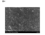
- FIG. 3 is a schematic cross-sectional view illustrating MXene forming the conductive film of the present embodiment; It is a schematic cross-sectional view for explaining a conventional conductive film. It is a schematic cross-sectional view for explaining the conductive film of the present embodiment. It is a scanning electron micrograph in an example.
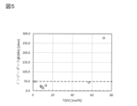
- FIG. 4 is a diagram showing the relationship between the proportion of tetravalent titanium and the impedance at 10 Hz of an electrode with a diameter of 10 mm in Examples.
- the conductive film in this embodiment is a film comprising particles of a layered material comprising one or more layers; and titanium oxide;
- the layer has the following formula: M m X n (wherein M is at least one Group 3, 4, 5, 6, 7 metal, including Ti, X is a carbon atom, a nitrogen atom, or a combination thereof; n is 1 or more and 4 or less, m is greater than n and less than or equal to 5) and a modification or termination T (T is at least one selected from the group consisting of a hydroxyl group, a fluorine atom, a chlorine atom, an oxygen atom and a hydrogen atom) present on the surface of the layer body represented by and
- T is at least one selected from the group consisting of a hydroxyl group, a fluorine atom, a chlorine atom, an oxygen atom and a hydrogen atom
- a film containing particles of a layered material containing one or more layers, which constitutes the conductive film of the present embodiment, will be described below.
- the layered material may be understood as a layered compound, also denoted as "M m X n T s ", where s is any number, conventionally x or z may be used instead of s.
- n can be 1, 2, 3 or 4, but is not so limited.
- M may be Ti only, or has Ti and at least one selected from the group consisting of Zr, Hf, V, Nb, Ta, Cr, Mo and Mn may have one.
- M contains an element other than Ti
- the element other than Ti is more preferably at least one selected from the group consisting of V, Cr and Mo.
- MXene is known in which the above formula: M m X n is expressed as follows.
- M can be titanium or titanium and vanadium and X can be a carbon or nitrogen atom.
- MAX phase is Ti 3 AlC 2 and MXene is Ti 3 C 2 T s (in other words, M is Ti, X is C, n is 2, m is 3 is).
- MXene may contain a relatively small amount of residual A atoms, for example, 10% by mass or less relative to the original A atoms.
- the residual amount of A atoms can be preferably 8% by mass or less, more preferably 6% by mass or less. However, even if the residual amount of A atoms exceeds 10% by mass, there may be no problem depending on the application and usage conditions of the conductive film and the electrode.
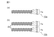
- the MXene that constitutes the MXene particles according to the present embodiment will be described below with reference to FIG.
- the MXene particles containing titanium oxide according to the present embodiment have substantially the same structure as the MXene particles forming the precursor film.
- FIG. 1 illustrates the structure corresponding to the skeleton of MXene particles containing titanium oxide, and titanium oxide is not shown in FIG.
- the MXene particle according to the present embodiment is an aggregate containing a plurality of one layer of MXene 10a (single layer MXene) schematically illustrated in FIG. 1(a). More specifically, the MXene 10a includes a layer body (M m X n layer) 1a represented by M m X n and a surface of the layer body 1a (more specifically, at least one of the two surfaces of the layer body 1a) MXene layer 7a with modifications or terminations T3a, 5a present in . Therefore, the MXene layer 7a is also expressed as "M m X n T s ", where s is any number.
- MXene can be one layer or multiple layers.
- a multi-layer MXene includes a two-layer MXene 10b as schematically shown in FIG. 1(b), but is not limited to these examples.
- 1b, 3b, 5b and 7b in FIG. 1(b) are the same as 1a, 3a, 5a and 7a in FIG. 1(a) described above.
- Two adjacent MXene layers (eg 7a and 7b) of a multi-layer MXene are not necessarily completely separated and may be in partial contact.
- the MXene 10a exists in one layer with the multilayer MXene 10b separated individually, and the multilayer MXene 10b that is not separated may remain and be a mixture of the single-layer MXene 10a and the multilayer MXene 10b. Even when the multi-layered MXene is included, the multi-layered MXene is preferably MXene with a small number of layers obtained through a delamination treatment.
- the phrase “the number of layers is small” means, for example, that the number of layers of MXene is 10 or less.
- this "multilayer MXene with a small number of layers" may be referred to as a "small layer MXene".
- the thickness of the small-layer MXene in the stacking direction may be 15 nm or less, and may be 10 nm or less.
- single-layer MXene and small-layer MXene may be collectively referred to as "single-layer/small-layer MXene".
- MXenes may be single-layer/small-layer MXenes. Since many of the MXenes are single-layer or few-layer MXenes, the specific surface area of the MXenes can be made larger than that of the multilayer MXenes. Deterioration of electrical conductivity over time can be suppressed.
- single-layer/small-layer MXene having a lamination number of 10 layers or less and a thickness of 15 nm or less, preferably 10 nm or less may account for, for example, 80% by volume or more of the total MXene. It may be 90% by volume or more, or even 95% by volume or more.
- the volume of single-layer MXene may be greater than the volume of low-layer MXene. Since the true densities of these MXenes do not vary greatly depending on their forms of existence, it can be said that the mass of single-layer MXenes is greater than the mass of small-layer MXenes. When these relationships are satisfied, the specific surface area of MXene can be increased, and deterioration of the conductivity over time can be suppressed when used in applications requiring the above-described conductivity.
- the film may be formed of only a single layer of MXene.
- each MXene layer (corresponding to the MXene layers 7a and 7b described above) can be, for example, 1 nm or more and 30 ⁇ m or less, for example, 1 nm or more and 5 nm or less, Furthermore, it may be 1 nm or more and 3 nm or less (mainly, it may vary depending on the number of M atomic layers included in each layer).
- the interlayer distance (or void dimension, indicated by ⁇ d in FIG. 1(b)) is, for example, ⁇ 0.8 nm and ⁇ 10 nm, especially ⁇ 0.8 nm and ⁇ 5 nm. Below, more particularly about 1 nm, the total number of layers can be from 2 to 20,000.
- the conductive film of this embodiment contains titanium oxide.
- the ratio of titanium oxide contained in the conductive film is evaluated by the ratio of tetravalent titanium constituting titanium oxide. That is, titanium includes divalent and trivalent titanium that form, for example, the structure of MXene, in addition to tetravalent titanium that constitutes titanium oxide.
- the ratio of tetravalent titanium to divalent, trivalent and tetravalent titanium obtained from the spectrum obtained by X-ray photoelectron spectroscopy (XPS) is 2 mol%. more than 57 mol % or less. Within the above range, it is believed that titanium oxide can partially change the structure of the MXene film as described below and increase the conductivity without lowering the inherent conductivity of the MXene film. .
- FIG. 2 is a cross-sectional view schematically showing a conventional conductive film.
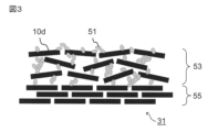
- FIG. 3 is a cross-sectional view schematically showing the conductive film according to this embodiment.
- FIG. 3 is only an image diagram used for convenience of explanation, and the shape of the crystals of titanium oxide, the form such as size, the arrangement in the MXene film, the arrangement of the MXene particles, etc. are expressed for ease of explanation. and is not limited to the form shown in FIG.
- this embodiment is not bound by any theory, the reason why the conductive film according to this embodiment exhibits excellent conductivity is presumed as follows. That is, as shown in FIG.
- the internal region 55 deeper than the outermost surface of the conductive film is considered to have MXene layers laminated and to exhibit the effect of MXene as an extraction electrode.
- the decrease in impedance due to the above effect is sufficiently manifested while suppressing the increase in impedance due to titanium oxide, thereby exhibiting high conductivity.
- the titanium oxide is preferably obtained by oxidizing titanium, which constitutes MXene, by aging, which will be described later.
- the electrode according to this embodiment includes the conductive film.
- the electrode may be formed only from the conductive film, or may include the conductive film and, for example, a base material.
- Electrodes include those in a solid state to those in a flexible soft state.
- Impedance is one of the characteristics of the electrodes of this embodiment. According to the measurement conditions described later in Examples, for example, at 10 Hz, it is preferably 49.0 ohms or less, more preferably 45.0 ohms or less, and even more preferably 30.0 ohms or less.
- the conductive film may be exposed to the open air so as to be in direct contact with the object to be measured, or may be another laminate such as a gel permeable to ions, or a porous film.
- a film or the like containing may be formed.
- the porous membrane may be a membrane that has a large number of fine pores and selectively permeates ions and molecules smaller in size than the diameter of the pores.
- Materials for these other laminates are not particularly limited, and may be formed of an organic material, an inorganic material, or a mixture thereof.
- organic materials include polymers such as hydrophilic polymers, and inorganic materials include ceramics, or combinations thereof.
- the film thickness of these other laminates can be, for example, 0.1 ⁇ m or more and 300 ⁇ m or less.
- the porous membrane may have, for example, an average pore size of 1 nm or more and 1 ⁇ m or less.
- Examples of the porous membrane include agglomerated particulate porous membranes, network porous membranes, fibrous porous membranes, porous membranes having a plurality of isolated and/or communicating pores, honeycomb structured porous membranes, and the like, depending on the pore shape. .
- the conductive film and the base material may be in direct contact.
- the material of the base material is not particularly limited.
- the base material is made of a conductive material.
- the conductive material includes at least one of metal materials such as gold, silver, copper, platinum, nickel, titanium, tin, iron, zinc, magnesium, aluminum, tungsten, molybdenum, and a conductive polymer. be done.
- the substrate may have a conductive film such as a metal film on the contact surface with the conductive film according to the present embodiment, which is different from the conductive film according to the present embodiment.
- the base material may be made of an organic material. Examples of the organic material include flexible organic materials such as thermoplastic polyurethane elastomer (TPU), PET film, and polyimide film.
- Electrodes of the present embodiments may be utilized for any suitable application. Examples thereof include bioelectrodes, battery electrodes, counter electrodes and reference electrodes for electrochemical measurements, electrodes for electrochemical capacitors, and the like. It can also be used in applications where maintaining high conductivity (reducing initial conductivity loss and preventing oxidation) is required, such as electromagnetic shielding (EMI shielding). Details of these applications are described below.
- EMI shielding electromagnetic shielding
- the electrodes are not particularly limited, but may be, for example, capacitor electrodes, battery electrodes, biosignal sensing electrodes, sensor electrodes, antenna electrodes, and the like.
- capacitor electrodes battery electrodes
- biosignal sensing electrodes sensor electrodes
- antenna electrodes and the like.
- the conductive film of this embodiment it is possible to obtain a large-capacity capacitor and battery, a low-impedance biosignal sensing electrode, a highly sensitive sensor and an antenna, even with a smaller volume (equipment occupied volume).
- the capacitor can be an electrochemical capacitor.
- An electrochemical capacitor is a capacitor that utilizes the capacity that is generated due to the physicochemical reaction between an electrode (electrode active material) and ions in an electrolyte (electrolyte ion). device).
- the battery can be a chemical cell that can be repeatedly charged and discharged.
- the battery can be, for example, but not limited to, a lithium ion battery, a magnesium ion battery, a lithium sulfur battery, a sodium ion battery, and the like.
- a biosignal sensing electrode is an electrode for acquiring biosignals.
- the biosignal sensing electrodes can be, but are not limited to, electrodes for measuring EEG (electroencephalogram), ECG (electrocardiogram), EMG (electromyography), EIT (electrical impedance tomography), for example.
- the sensor electrode is an electrode for detecting the target substance, state, abnormality, etc.
- the sensor can be, for example, a gas sensor, a biosensor (a chemical sensor that utilizes a biogenic molecular recognition mechanism), or the like, but is not limited thereto.
- the antenna electrode is an electrode for radiating electromagnetic waves into space and/or receiving electromagnetic waves in space.
- the electrode of this embodiment is preferably used as a biosignal sensing electrode.
- the conductive film composed of MXene containing an appropriate amount of titanium oxide there is almost no increase in impedance due to titanium oxide, and it is thought that the impedance decreases as the distance between MXene flakes in the surface region increases. . As a result, it is considered that the sensitivity becomes higher when used as a biosignal sensing electrode.
- a manufacturing method (first manufacturing method) of one conductive film of the present embodiment includes: (a) particles of a layered material comprising one or more layers, The layer has the following formula: M m X n (wherein M is at least one Group 3, 4, 5, 6, 7 metal, including Ti, X is a carbon atom, a nitrogen atom, or a combination thereof; n is 1 or more and 4 or less, m is greater than n and less than or equal to 5) and a modification or termination T (T is at least one selected from the group consisting of a hydroxyl group, a fluorine atom, a chlorine atom, an oxygen atom and a hydrogen atom) present on the surface of the layer body represented by providing particles of a layered material comprising (b) using the particles of the layered material to form a precursor film comprising the particles of the layered material; (c) aging the precursor film to obtain a conductive film, wherein the conductive film comprises divalent, trivalent and tetravalent titanium as determined from
- Another conductive film manufacturing method (second manufacturing method) of the present embodiment includes: (A) a particle of a layered material comprising one or more layers, The layer has the following formula: M m X n (wherein M is at least one Group 3, 4, 5, 6, 7 metal, including Ti, X is a carbon atom, a nitrogen atom, or a combination thereof; n is 1 or more and 4 or less, m is greater than n and less than or equal to 5) and a modification or termination T (T is at least one selected from the group consisting of a hydroxyl group, a fluorine atom, a chlorine atom, an oxygen atom and a hydrogen atom) present on the surface of the layer body represented by providing particles of a layered material comprising (B) aging a dispersion containing particles of the layered material; (C) forming a conductive film containing particles of the layered material using a dispersion containing the particles of the aged layered material, the conductive film being measured by X-ray photo
- a method for producing a conductive film wherein the ratio of tetravalent titanium to divalent, trivalent and tetravalent titanium determined from the obtained spectrum is more than 2 mol % and 57 mol % or less.
- a predetermined precursor that can be used in this embodiment is the MAX phase, which is a precursor of MXene, The formula below: M m AX n (wherein M is at least one Group 3, 4, 5, 6, 7 metal, including Ti, X is a carbon atom, a nitrogen atom, or a combination thereof; A is at least one Group 12, 13, 14, 15, 16 element; n is 1 or more and 4 or less, m is greater than n and less than or equal to 5) is represented by
- A is at least one Group 12, 13, 14, 15, 16 element, usually a Group A element, typically Groups IIIA and IVA, more particularly Al, Ga, In, It may contain at least one selected from the group consisting of Tl, Si, Ge, Sn, Pb, P, As, S and Cd, preferably Al.
- a MAX phase is a crystal in which a layer composed of A atoms is located between two layers denoted by M m X n (each X may have a crystal lattice located in an octahedral array of M). have a structure.
- the MAX phase can be produced by a known method. For example, TiC powder, Ti powder and Al powder are mixed in a ball mill, and the resulting mixed powder is fired in an Ar atmosphere to obtain a fired body (block-shaped MAX phase). After that, the obtained sintered body can be pulverized with an end mill to obtain a powdery MAX phase for the next step.
- a atomic layer (and optionally part of M atoms) is removed by selectively etching (removing and optionally layer separation) A atoms (and optionally part of M atoms) from the MAX phase.
- a atoms (and optionally part of M atoms) from the MAX phase.
- hydroxyl groups, fluorine atoms, chlorine atoms, oxygen atoms, hydrogen atoms, etc. present in the etching solution (usually, but not limited to, an aqueous solution of fluorine-containing acid is used) on the exposed surface of the M m X n layer. Modify and terminate such surfaces.
- the etching can be performed using an etchant containing F 2 , such as a method using a mixed solution of lithium fluoride and hydrochloric acid or a method using hydrofluoric acid.
- the etching solution may contain a metal compound containing monovalent metal ions, and an intercalation treatment of the monovalent metal ions may be performed simultaneously with the etching.
- metal compounds containing monovalent metal ions include those used in the following intercalation treatment.
- the content of the metal compound containing monovalent metal ions in the etching solution is preferably 0.001% by mass or more. The above content is more preferably 0.01% by mass or more, still more preferably 0.1% by mass or more.
- the content of the metal compound containing monovalent metal ions in the etching solution is preferably 10% by mass or less, more preferably 1% by mass or less.
- any suitable post-treatment e.g. sonication, handshake or automatic shaker, etc.
- sonication may cause too much shear force to destroy the MXene, so if it is desired to obtain a two-dimensional shaped MXene with a higher aspect ratio (preferably a single-layer MXene), a handshake or Appropriate shearing force is preferably applied by an automatic shaker or the like.
- the following intercalation treatment and delamination may be performed.
- an intercalation treatment of monovalent metal ions may be performed, which includes a step of mixing the etched product obtained by the etching treatment with a metal compound containing monovalent metal ions.
- monovalent metal ions constituting metal compounds containing monovalent metal ions include alkali metal ions such as lithium ions, sodium ions and potassium ions, copper ions, silver ions, and gold ions.
- metal compounds containing monovalent metal ions include ionic compounds in which the above metal ions and cations are combined. Examples include iodides, phosphates, sulfide salts including sulfates, nitrates, acetates, and carboxylates of the above metal ions.
- the monovalent metal ion is preferably a lithium ion
- the metal compound containing a monovalent metal ion is preferably a metal compound containing a lithium ion, and more preferably an ionic compound of a lithium ion.
- One or more of acid salts and sulfide salts are more preferred. If lithium ions are used as the metal ions, the water hydrated with the lithium ions has the most negative dielectric constant, so it is considered that the monolayer is easily formed.
- the content of the metal compound containing monovalent metal ions in the compound for intercalation treatment of monovalent metal ions is preferably 0.001% by mass or more.
- the above content is more preferably 0.01% by mass or more, still more preferably 0.1% by mass or more.
- the content of the metal compound containing monovalent metal ions is preferably 10% by mass or less, more preferably 1% by mass or less.
- delamination is performed using an intercalated product obtained by intercalation.
- delamination includes a step of centrifuging the intercalated product, discarding the supernatant, and washing the remaining precipitate with water.
- Conditions for the delamination treatment are not particularly limited.
- the dispersion medium used for delamination is also not particularly limited, and for example, one or more of a polar organic dispersion medium and an aqueous dispersion medium may be used. One or more of the polar organic dispersion medium and the aqueous dispersion medium are added, stirred, and centrifuged to collect the supernatant, which is repeated one or more times, preferably two or more times, and ten times or less.
- a supernatant containing a small amount of MXene is obtained as a delamination product.
- the supernatant may be centrifuged and the supernatant after centrifugation may be discarded to obtain single-layer/small-layer MXene-containing clay as a delaminated product.
- the particles of the layered material are used to form a precursor film containing the particles of the layered material.
- a dispersion of layered material particles such as MXene slurry obtained by diluting the above single-layer/small-layer MXene-containing clay with a medium liquid can be used.
- a dispersion may be a suspension.
- the method of forming the MXene film using the dispersion of MXene particles is not particularly limited.
- a dispersion of MXene particles may be applied to a substrate as it is or after suitable adjustment (eg, dilution with a medium liquid or addition of a binder).
- Examples of the coating method include a method of spray coating using a nozzle such as a one-fluid nozzle, a two-fluid nozzle, and an airbrush (method using a spray coater), a table coater, a comma coater, a slit coat using a bar coater, and a screen. Printing, metal mask printing, spin coating, dip coating, dropping, and the like can be mentioned.
- Examples of the medium liquid include aqueous medium liquids and organic medium liquids.
- the medium liquid that constitutes the dispersion of the MXene particles is typically water, and in some cases, in addition to water, a relatively small amount of other liquid substance (for example, 30% by mass or less, preferably 20% by mass on the whole basis) % or less).
- Examples of the organic medium liquid include N-methylpyrrolidone, N-methylformamide, N,N-dimethylformamide, ethanol, methanol, dimethylsulfoxide, ethylene glycol, and acetic acid.
- MXene slurry is applied to a substrate such as PET or polyimide at an atomization pressure of 0.1 MPa or more and 0.5 MPa or less, and a nozzle tip and substrate distance of 10 cm or more and 25 cm or less.
- a substrate such as PET or polyimide
- the liquid feed rate to 0.1 mL/s to 10 mL/s
- the sweep speed to 1 mm/s to 30 mm/s
- the stage heater to 30 ° C. to 60 ° C., once or multiple times Forming a film (electrode) before drying by coating may be mentioned.
- the MXene membrane may be produced by suction filtering the slurry or the supernatant containing MXene particles obtained by the delamination. More specifically, as a dispersion of MXene particles, for example, a supernatant containing MXene particles is appropriately adjusted (for example, diluted with an aqueous medium liquid), and a filter (which constitutes a predetermined member together with the MXene membrane) is placed on a Nutsche or the like.
- the MXene membrane can be formed on the filter by suction filtering through a filter, which may eventually be separated from the MXene membrane, to at least partially remove the aqueous medium liquid.
- the filter is not particularly limited, a membrane filter or the like can be used.
- the MXene membrane can be produced without using the binder or the like.
- an MXene film can be produced without using a binder or the like.
- the material constituting the substrate is not particularly limited, and can be made of any appropriate material.
- the base material may be, for example, a resin film, a metal foil, a printed wiring board, a mounted electronic component, a metal pin, a metal wiring, a metal wire, or the like.
- a substrate formed of a metal material, resin, or the like suitable for a biosignal sensing electrode can be used as appropriate.
- An MXene membrane is formed on any suitable substrate (either one that constitutes a given member together with the MXene membrane or that is ultimately separated from the MXene membrane) by coating on the substrate. can be formed.
- Drying can be done under mild conditions such as natural drying (typically placed in an air atmosphere at normal temperature and pressure) or air drying (blowing air), or hot air drying (blowing heated air). ), heat drying, and/or vacuum drying.
- "Drying" in this embodiment means removing the medium liquid that may be present in the precursor. The drying may be performed at a temperature of 400° C. or less using, for example, a normal pressure oven or a vacuum oven. For example, it may be dried at 30° C. or higher and 200° C. or lower for 30 minutes or longer and 24 hours or shorter.
- the MXene film may be repeated as appropriate until the desired MXene film thickness is obtained. For example, the combination of spraying and drying may be repeated multiple times.
- the MXene membrane can be formed without containing a binder.
- the MXene membrane may or may not be substantially free of liquid components derived from the liquid medium of the slurry.
- the aging conditions are particularly Not limited.
- the precursor film may be left for 24 hours or more and 30 days or less under conditions of a temperature of 30° C. or more and 200° C. or less and a humidity of 45 RH% or more and 99 RH% or less.
- the condition that the proportion of tetravalent titanium is in the range of more than 2 mol % and 57 mol % or less may be appropriately set. Within the range of the above conditions, if the temperature is low, it takes time for oxidation, so the required aging time should be longer.
- the aging time may be 30 days or less, which is a longer required time.
- the temperature is 80° C. or higher, for example, as in the examples described below, the upper limit of the aging time may be 7 days or less.
- the temperature is more preferably 150° C. or lower, and even more preferably 100° C. or lower.
- the aging time can be less than 14 days, for example.
- the temperature may be set to, for example, 40° C. or higher.
- the humidity may be set to, for example, 50 RH% or higher, and further 60 RH% or higher.
- the atmosphere for aging other than the above is not limited, and may be, for example, an oxygen-containing atmosphere such as air.
- various electrodes can be manufactured at the same time, for example, after manufacturing a plurality of conductive films as electrodes, some electrodes (conductive films) are aged according to the application. and, for example, manufacturing costs can be reduced.
- the dispersion containing the particles of the layered material is aged.
- the aging conditions include leaving the dispersion containing the particles of the layered material at a temperature of 30° C. or more and 200° C. or less for 24 hours or more and 1 month or less (for example, 30 days or less).
- the aging time can be less than 14 days, for example.
- ⁇ Process (C) In the second production method, using a dispersion containing particles of the layered material subjected to aging, 4 A conductive film is formed comprising particles of the layered material having a proportion of valent titanium of more than 2 mol % and not more than 57 mol %.
- the method of forming the film using the dispersion containing the aged layered material particles may be the same as the step (b) in the first manufacturing method.
- the second manufacturing method for example, by performing aging in a slurry state, it is possible to manufacture a large amount of aged electrodes (conductive films) at once, leading to a reduction in manufacturing costs.
- the conductive film obtained by the second manufacturing method also exhibits the same degree of oxidation and impedance values as those of the conductive film obtained by the first manufacturing method. From this, it is considered that the conductive film obtained by the second production method also has the same form of titanium oxide as the conductive film obtained by the first production method.
- the particles of the layered material in the dispersion liquid are substantially uniformly aged in the step (B)
- the particles of the layered material that have been aged in the step (C) are included. It is presumed that titanium oxide moves to the outermost surface of the conductive film by, for example, shearing force when the dispersion is sprayed to form the conductive film. It is conceivable that such speculation is similarly generated in forming methods other than the above-described spraying method.
- Example 1 Preparation of Layered Material Particles Detailed below: (1) Precursor (MAX) preparation, (2) Precursor etching, (3) Post-etching cleaning, (4) Li intercalation, (5) ) Delamination was performed in order to obtain MXene particles first.
- Precursor (MAX) preparation TiC powder, Ti powder and Al powder (all manufactured by Kojundo Chemical Laboratory Co., Ltd.) were placed in a ball mill containing zirconia balls at a molar ratio of 2:1:1. mixed for 24 hours. The obtained mixed powder was fired at 1350° C. for 2 hours in an Ar atmosphere. The resulting sintered body (block-shaped MAX) was pulverized with an end mill to a maximum dimension of 40 ⁇ m or less. This gave Ti 3 AlC 2 particles as a precursor (powdered MAX).
- Li intercalation For the Ti 3 C 2 T s -water medium clay prepared by the above method, under the following Li intercalation conditions, LiCl was used as the Li-containing compound, and Li intercalation was performed by stirring for 12 hours.
- Detailed conditions for Li intercalation are as follows. (Conditions for Li intercalation) Ti 3 C 2 T s -water-borne clay (MXene after washing): 0.75 g solids ⁇ LiCl: 0.75 g ⁇ Intercalation container: 100 mL eyeboy ⁇ Temperature: 20°C or higher and 25°C or lower (room temperature) ⁇ Time: 12 hours ⁇ Stirrer rotation speed: 800 rpm
- this supernatant is centrifuged at 4300 G for 2 hours using a centrifuge, and then the supernatant is discarded to obtain MXene clay containing single-layer/low-layer MXene as the remaining precipitate. rice field.
- MXene Slurry A predetermined amount of the MXene clay obtained in 1 above was placed in a 50 mL centrifuge tube, and pure water was added so that the concentration of MXene was 1.5 wt %. After that, the mixture was stirred for 15 minutes using a shaker to obtain an MXene slurry.
- Electrode Sample No. in Table 1 obtained in 2 above. MXene slurries from 6 to 8, or no. Electrode samples were made using 2-5 aged MXene slurries and performed in the following order.
- the frequency is in the range of 0.1 Hz to 106 Hz
- the voltage is an open circuit voltage, or 1 mVrms to 20 mVrms with respect to the reference pole
- the number of plots is 71
- the number of N per plot is 1. Measurements were made in potentiostat mode with each setting of ⁇ 10.
- VMP-300 high-performance electrochemical measurement system (16ch, advanced model) manufactured by Bio-Logic Science Instruments was used as an apparatus. Table 1 shows the impedance at 10 Hz of an electrode with a diameter of 10 mm as a measurement result.
- the degree of oxidation was measured by XPS as follows.
- the ratio of spectral peaks of tetravalent Ti was calculated as the ratio of tetravalent Ti when the sum of the areas of these spectral peaks was taken as 100, and this calculated value was defined as the "degree of oxidation".
- the detection depth in the thickness direction of the XPS film is about 5 nm, and information on the outermost surface is detected. Also, information on a range of 1000 ⁇ m ⁇ 200 ⁇ m was obtained by scanning X-rays with a diameter of 100 ⁇ m instead of information on a specific point. Table 1 shows the measurement results.
- the upper limit of the time required for aging to obtain an MXene film having a tetravalent titanium ratio of 57 mol % or less is It was 7 days.
- the degree of oxidation of the peeled surface was lower than that of the surface for all samples.
- the ratio of tetravalent titanium on the peeled surface of the film is, for example, sample No. 8 was 7 mol %, and oxidation was suppressed.
- the conductive film according to the present embodiment can be used for any appropriate application, it can be preferably used for applications that require high conductivity, and can be particularly preferably used as an electrode, for example.
- MXene (particles) 30 conventional MXene film 31 MXene film according to the present embodiment 51 crystals of titanium oxide 53 surface region of MXene film 55 internal region of MXene film
Landscapes
- Engineering & Computer Science (AREA)
- Chemical & Material Sciences (AREA)
- Power Engineering (AREA)
- Materials Engineering (AREA)
- Microelectronics & Electronic Packaging (AREA)
- Chemical Kinetics & Catalysis (AREA)
- Electrochemistry (AREA)
- General Chemical & Material Sciences (AREA)
- Manufacturing & Machinery (AREA)
- Organic Chemistry (AREA)
- Nanotechnology (AREA)
- Physics & Mathematics (AREA)
- Dispersion Chemistry (AREA)
- Spectroscopy & Molecular Physics (AREA)
- Life Sciences & Earth Sciences (AREA)
- Environmental & Geological Engineering (AREA)
- General Life Sciences & Earth Sciences (AREA)
- Geology (AREA)
- Inorganic Chemistry (AREA)
- Crystallography & Structural Chemistry (AREA)
- Inorganic Compounds Of Heavy Metals (AREA)
Abstract
L'invention concerne un film conducteur contenant du MXène et ayant une impédance suffisamment faible. Le film conducteur contient de l'oxyde de titane et un film qui contient des particules d'un matériau stratifié comprenant une ou plusieurs couches, dans lequel : les couches comprennent chacune un corps de couche représenté par la formule MmXn (dans la formule, M représente au moins un métal appartenant au groupe 3, 4, 5, 6, ou 7 et comprend du Ti, X représente un atome de carbone, un atome d'azote ou une combinaison de ceux-ci, n vaut de 1 à 4, et m est supérieur à n et inférieur ou égal à 5) et une modification ou un T terminal (T représente au moins un élément choisi dans le groupe constitué par un groupe hydroxyle, un atome de fluor, un atome de chlore, un atome d'oxygène et un atome d'hydrogène) est présent sur la surface du corps de couche ; et la proportion de titane tétravalent dans le titane divalent, trivalent et tétravalent, telle que déterminée par des spectres obtenus par spectroscopie photoélectronique à rayons X, est de 2 à 57 % en moles (à l'exclusion de 2).
Priority Applications (3)
| Application Number | Priority Date | Filing Date | Title |
|---|---|---|---|
| JP2023566249A JPWO2023106153A1 (fr) | 2021-12-08 | 2022-11-28 | |
| CN202280081154.0A CN118369738A (zh) | 2021-12-08 | 2022-11-28 | 导电性膜、电极以及导电性膜的制造方法 |
| US18/736,757 US20240321475A1 (en) | 2021-12-08 | 2024-06-07 | Conductive film, electrode, and method for producing conductive film |
Applications Claiming Priority (2)
| Application Number | Priority Date | Filing Date | Title |
|---|---|---|---|
| JP2021-199517 | 2021-12-08 | ||
| JP2021199517 | 2021-12-08 |
Related Child Applications (1)
| Application Number | Title | Priority Date | Filing Date |
|---|---|---|---|
| US18/736,757 Continuation US20240321475A1 (en) | 2021-12-08 | 2024-06-07 | Conductive film, electrode, and method for producing conductive film |
Publications (1)
| Publication Number | Publication Date |
|---|---|
| WO2023106153A1 true WO2023106153A1 (fr) | 2023-06-15 |
Family
ID=86730215
Family Applications (1)
| Application Number | Title | Priority Date | Filing Date |
|---|---|---|---|
| PCT/JP2022/043779 WO2023106153A1 (fr) | 2021-12-08 | 2022-11-28 | Film conducteur, électrode et procédé de fabrication de film conducteur |
Country Status (4)
| Country | Link |
|---|---|
| US (1) | US20240321475A1 (fr) |
| JP (1) | JPWO2023106153A1 (fr) |
| CN (1) | CN118369738A (fr) |
| WO (1) | WO2023106153A1 (fr) |
Citations (3)
| Publication number | Priority date | Publication date | Assignee | Title |
|---|---|---|---|---|
| JP2020093971A (ja) * | 2018-10-02 | 2020-06-18 | コリア・インスティテュート・オブ・サイエンス・アンド・テクノロジー | 飽和または不飽和炭化水素を含む官能基で表面改質された2次元マキシン(MXene)粒子及びその製造方法及び用途 |
| WO2021025026A1 (fr) * | 2019-08-05 | 2021-02-11 | 株式会社村田製作所 | Matériau conducteur, film conducteur, condensateur électrochimique, procédé de production de matériau conducteur et procédé de production de film conducteur |
| WO2021131643A1 (fr) * | 2019-12-25 | 2021-07-01 | 株式会社村田製作所 | Structure composite électroconductrice et procédé de production associé |
-
2022
- 2022-11-28 JP JP2023566249A patent/JPWO2023106153A1/ja active Pending
- 2022-11-28 CN CN202280081154.0A patent/CN118369738A/zh active Pending
- 2022-11-28 WO PCT/JP2022/043779 patent/WO2023106153A1/fr unknown
-
2024
- 2024-06-07 US US18/736,757 patent/US20240321475A1/en active Pending
Patent Citations (3)
| Publication number | Priority date | Publication date | Assignee | Title |
|---|---|---|---|---|
| JP2020093971A (ja) * | 2018-10-02 | 2020-06-18 | コリア・インスティテュート・オブ・サイエンス・アンド・テクノロジー | 飽和または不飽和炭化水素を含む官能基で表面改質された2次元マキシン(MXene)粒子及びその製造方法及び用途 |
| WO2021025026A1 (fr) * | 2019-08-05 | 2021-02-11 | 株式会社村田製作所 | Matériau conducteur, film conducteur, condensateur électrochimique, procédé de production de matériau conducteur et procédé de production de film conducteur |
| WO2021131643A1 (fr) * | 2019-12-25 | 2021-07-01 | 株式会社村田製作所 | Structure composite électroconductrice et procédé de production associé |
Also Published As
| Publication number | Publication date |
|---|---|
| CN118369738A (zh) | 2024-07-19 |
| JPWO2023106153A1 (fr) | 2023-06-15 |
| US20240321475A1 (en) | 2024-09-26 |
Similar Documents
| Publication | Publication Date | Title |
|---|---|---|
| JP7513110B2 (ja) | 導電性2次元粒子およびその製造方法、導電性膜、導電性複合材料、ならびに導電性ペースト | |
| JP7164055B2 (ja) | 導電性複合構造体およびその製造方法 | |
| WO2023047861A1 (fr) | Composition contenant des particules bidimensionnelles conductrices, film conducteur, et procédé de fabrication d'une composition contenant des particules bidimensionnelles conductrices | |
| US20240034634A9 (en) | Conductive two-dimensional particle and method for producing the same | |
| US20230352205A1 (en) | Conductive film and method for producing the same | |
| JP7355249B2 (ja) | 膜の製造方法および導電性膜 | |
| US20230233127A1 (en) | Biosignal sensing electrode | |
| WO2023248598A1 (fr) | Film et son procédé de production | |
| WO2023106153A1 (fr) | Film conducteur, électrode et procédé de fabrication de film conducteur | |
| US20230187098A1 (en) | Conductive film and method for producing same | |
| JP7487783B2 (ja) | 導電性2次元粒子およびその製造方法 | |
| WO2024162390A1 (fr) | Électrode et procédé de fabrication d'électrode | |
| WO2023233783A1 (fr) | Électrode et procédé de fabrication d'électrode | |
| WO2023002916A1 (fr) | Électrode et son procédé de production | |
| WO2023162423A1 (fr) | Particule bidimensionnelle, méthode de production de particule bidimensionnelle et matériau | |
| WO2023002915A1 (fr) | Électrode et son procédé de production | |
| WO2024203470A1 (fr) | Particule bidimensionnelle, et film électroconducteur et son procédé de production | |
| WO2023112778A1 (fr) | Particule bidimensionnelle, film électroconducteur, pâte électroconductrice et matériau composite | |
| WO2024185855A1 (fr) | Composition contenant des particules bidimensionnelles et méthode de production d'une composition contenant des particules bidimensionnelles | |
| JP2024535287A (ja) | 2次元粒子、導電性膜、導電性ペーストおよび2次元粒子の製造方法 | |
| WO2023149103A1 (fr) | Matériau composite et procédé de production de structure de matériau composite | |
| US20240175841A1 (en) | Biosignal sensing electrode |
Legal Events
| Date | Code | Title | Description |
|---|---|---|---|
| 121 | Ep: the epo has been informed by wipo that ep was designated in this application |
Ref document number: 22904084 Country of ref document: EP Kind code of ref document: A1 |
|
| ENP | Entry into the national phase |
Ref document number: 2023566249 Country of ref document: JP Kind code of ref document: A |
|
| NENP | Non-entry into the national phase |
Ref country code: DE |