WO2023100694A1 - 電極基板 - Google Patents
電極基板 Download PDFInfo
- Publication number
- WO2023100694A1 WO2023100694A1 PCT/JP2022/042877 JP2022042877W WO2023100694A1 WO 2023100694 A1 WO2023100694 A1 WO 2023100694A1 JP 2022042877 W JP2022042877 W JP 2022042877W WO 2023100694 A1 WO2023100694 A1 WO 2023100694A1
- Authority
- WO
- WIPO (PCT)
- Prior art keywords
- layer
- silver chloride
- silver
- chloride layer
- electrode
- Prior art date
- Legal status (The legal status is an assumption and is not a legal conclusion. Google has not performed a legal analysis and makes no representation as to the accuracy of the status listed.)
- Ceased
Links
Images



Classifications
-
- H—ELECTRICITY
- H01—ELECTRIC ELEMENTS
- H01B—CABLES; CONDUCTORS; INSULATORS; SELECTION OF MATERIALS FOR THEIR CONDUCTIVE, INSULATING OR DIELECTRIC PROPERTIES
- H01B1/00—Conductors or conductive bodies characterised by the conductive materials; Selection of materials as conductors
- H01B1/02—Conductors or conductive bodies characterised by the conductive materials; Selection of materials as conductors mainly consisting of metals or alloys
-
- G—PHYSICS
- G01—MEASURING; TESTING
- G01N—INVESTIGATING OR ANALYSING MATERIALS BY DETERMINING THEIR CHEMICAL OR PHYSICAL PROPERTIES
- G01N27/00—Investigating or analysing materials by the use of electric, electrochemical, or magnetic means
- G01N27/26—Investigating or analysing materials by the use of electric, electrochemical, or magnetic means by investigating electrochemical variables; by using electrolysis or electrophoresis
- G01N27/28—Electrolytic cell components
-
- G—PHYSICS
- G01—MEASURING; TESTING
- G01N—INVESTIGATING OR ANALYSING MATERIALS BY DETERMINING THEIR CHEMICAL OR PHYSICAL PROPERTIES
- G01N27/00—Investigating or analysing materials by the use of electric, electrochemical, or magnetic means
- G01N27/26—Investigating or analysing materials by the use of electric, electrochemical, or magnetic means by investigating electrochemical variables; by using electrolysis or electrophoresis
- G01N27/28—Electrolytic cell components
- G01N27/30—Electrodes, e.g. test electrodes; Half-cells
-
- G—PHYSICS
- G01—MEASURING; TESTING
- G01N—INVESTIGATING OR ANALYSING MATERIALS BY DETERMINING THEIR CHEMICAL OR PHYSICAL PROPERTIES
- G01N27/00—Investigating or analysing materials by the use of electric, electrochemical, or magnetic means
- G01N27/26—Investigating or analysing materials by the use of electric, electrochemical, or magnetic means by investigating electrochemical variables; by using electrolysis or electrophoresis
- G01N27/28—Electrolytic cell components
- G01N27/30—Electrodes, e.g. test electrodes; Half-cells
- G01N27/301—Reference electrodes
-
- G—PHYSICS
- G01—MEASURING; TESTING
- G01N—INVESTIGATING OR ANALYSING MATERIALS BY DETERMINING THEIR CHEMICAL OR PHYSICAL PROPERTIES
- G01N27/00—Investigating or analysing materials by the use of electric, electrochemical, or magnetic means
- G01N27/26—Investigating or analysing materials by the use of electric, electrochemical, or magnetic means by investigating electrochemical variables; by using electrolysis or electrophoresis
- G01N27/28—Electrolytic cell components
- G01N27/30—Electrodes, e.g. test electrodes; Half-cells
- G01N27/327—Biochemical electrodes, e.g. electrical or mechanical details for in vitro measurements
-
- G—PHYSICS
- G01—MEASURING; TESTING
- G01N—INVESTIGATING OR ANALYSING MATERIALS BY DETERMINING THEIR CHEMICAL OR PHYSICAL PROPERTIES
- G01N27/00—Investigating or analysing materials by the use of electric, electrochemical, or magnetic means
- G01N27/26—Investigating or analysing materials by the use of electric, electrochemical, or magnetic means by investigating electrochemical variables; by using electrolysis or electrophoresis
- G01N27/403—Cells and electrode assemblies
- G01N27/414—Ion-sensitive or chemical field-effect transistors, i.e. ISFETS or CHEMFETS
-
- H—ELECTRICITY
- H01—ELECTRIC ELEMENTS
- H01B—CABLES; CONDUCTORS; INSULATORS; SELECTION OF MATERIALS FOR THEIR CONDUCTIVE, INSULATING OR DIELECTRIC PROPERTIES
- H01B5/00—Non-insulated conductors or conductive bodies characterised by their form
- H01B5/16—Non-insulated conductors or conductive bodies characterised by their form comprising conductive material in insulating or poorly conductive material, e.g. conductive rubber
-
- G—PHYSICS
- G01—MEASURING; TESTING
- G01N—INVESTIGATING OR ANALYSING MATERIALS BY DETERMINING THEIR CHEMICAL OR PHYSICAL PROPERTIES
- G01N27/00—Investigating or analysing materials by the use of electric, electrochemical, or magnetic means
- G01N27/26—Investigating or analysing materials by the use of electric, electrochemical, or magnetic means by investigating electrochemical variables; by using electrolysis or electrophoresis
- G01N27/28—Electrolytic cell components
- G01N27/30—Electrodes, e.g. test electrodes; Half-cells
- G01N27/327—Biochemical electrodes, e.g. electrical or mechanical details for in vitro measurements
- G01N27/3271—Amperometric enzyme electrodes for analytes in body fluids, e.g. glucose in blood
Definitions
- the present invention relates to electrode substrates.
- Patent Document 1 Japanese Patent Laid-Open No. 2005-292022 is a prior art document that discloses a method for manufacturing a reference electrode.
- the reference electrode described in Patent Document 1 includes a conductive pattern formed on an insulating substrate, and a composite containing silver formed on the reference electrode portion of the conductive pattern, and the surface of the composite is chlorinated. Consists of a silver layer.
- An electrode substrate based on the present invention comprises an insulating substrate and a reference electrode.
- a reference electrode is formed on an insulating substrate.
- the reference electrode includes a silver layer, a first silver chloride layer and a second silver chloride layer.
- a silver layer is formed on an insulating substrate.
- the first silver chloride layer is formed over the silver layer and the insulating substrate to cover the silver layer.
- the second silver chloride layer is formed over the first silver chloride layer and the insulating substrate to cover the first silver chloride layer.
- the areal porosity of the first silver chloride layer is greater than the areal porosity of the second silver chloride layer.
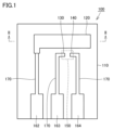
- FIG. 1 is a plan view showing the configuration of an electrode substrate according to one embodiment of the present invention
- FIG. 2 is a cross-sectional view of the electrode substrate of FIG. 1 as seen from the direction of arrows on line II-II.
- 1 is a perspective view schematically showing the configuration of a graphene transistor using an electrode substrate according to one embodiment of the present invention
- FIG. 10 is a partial vertical cross-sectional view showing shear stress distribution generated when temperature is changed from 20° C. to 100° C.
- FIG. 5 is a partial vertical cross-sectional view showing shear stress distribution generated when the temperature is changed from 20° C. to 100° C. in the reference electrode according to the present embodiment.
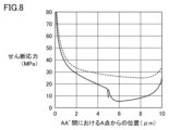
- 8 is a graph showing changes in shear stress at positions from point A between AA' along the interface between the insulating substrate and the silver chloride layer shown in FIGS. 6 and 7.
- FIG. 5 is a partial vertical cross-sectional view showing shear stress distribution generated when the temperature is changed from 20° C. to 100° C. in the reference electrode according to the present embodiment.
- 8 is a graph showing changes in shear stress at positions from point A between AA' along the interface between the insulating substrate and the silver chloride layer shown in FIGS. 6 and 7.
- FIG. 1 is a plan view showing the configuration of an electrode substrate according to one embodiment of the present invention.
- FIG. 2 is a cross-sectional view of the electrode substrate of FIG. 1 as viewed from the direction of the arrows on line II-II.
- an electrode substrate 100 according to one embodiment of the present invention includes an insulating substrate 110 and a reference electrode 120. As shown in FIG. A reference electrode 120 is formed on the insulating substrate 110 .
- the electrode substrate 100 further includes a metal wiring layer 170 formed on the insulating substrate 110 .
- a semiconductor such as silicon or germanium, glass such as quartz glass, lead glass or borosilicate glass, ceramics, resin, or the like can be used.
- the resin material forming the insulating substrate 110 includes polystyrene (PS), polypropylene (PP), polyimide (PI), polytetrafluoroethylene (PTFE), polyphenylene sulfide (PPS), polyetheretherketone (PEEK), and polyethylene.
- PS polystyrene
- PP polypropylene
- PI polyimide
- PTFE polytetrafluoroethylene
- PPS polyphenylene sulfide
- PEEK polyetheretherketone
- PET Terephthalate
- PMMA polymethyl methacrylate
- PEN polyethylene-2,6-naphthalate
- the insulating substrate 110 is made of silicon and has a SiO 2 film formed on its surface.
- metal wiring layer 170 As a material for the metal wiring layer 170, noble metals such as gold, platinum, or palladium, carbon, or the like can be used. From the viewpoint of the stability of the surface state, etc., it is preferable to form the metal wiring layer 170 with gold.
- a method of forming a wiring pattern on the insulating substrate 110 by sputtering using a mask can be considered.
- the surface portion of the SiO 2 film located at the position where the metal wiring layer 170 is to be formed is removed and thinned, a titanium layer is formed on the portion, and a gold layer is formed on the titanium layer.
- the metal wiring layer 170 has a laminated structure of a titanium layer and a gold layer.
- the thickness of the titanium layer is, for example, 10 nm.
- the thickness of the gold layer is, for example, 90 nm.
- the patterned metal wiring layer 170 forms the first connection terminal 162 , the second connection terminal 163 , the third connection terminal 164 , the first electrode 130 and the second electrode 140 .
- Each of the first connection terminal 162, the second connection terminal 163 and the third connection terminal 164 is formed along the edge of the insulating substrate 110 and can be electrically connected to an external terminal.
- the first connection terminal 162 is connected with the reference electrode 120 .
- the second connection terminal 163 is connected to the first electrode 130 .
- the third connection terminal 164 is connected with the second electrode 140 .
- the first electrode 130 and the second electrode 140 face each other with a gap therebetween.
- the first electrode 130 and the second electrode 140 are configured to be electrically connectable to each other through the transmission line 150 .
- the transmission line 150 is composed of a semiconductor channel. Specifically, the transmission line 150 is made of graphene. A pair of electrodes consisting of the first electrode 130 and the second electrode 140 are joined to a semiconductor channel formed in the insulating substrate 110 .
- the transmission line 150 is not limited to a semiconductor channel, and may be a solution such as blood placed on the electrode substrate 100 .
- the electrode substrate 100 can be applied to an enzyme sensor such as a glucose sensor.
- the reference electrode 120 includes a metal wiring layer 170, a silver layer 121, a first silver chloride layer 122, and a second silver chloride layer 123.
- the silver layer 121 is formed over the metal wiring layer 170 and the insulating substrate 110 to cover at least part of the metal wiring layer 170 . A portion of the silver layer 121 is formed on the insulating substrate 110 .
- the silver layer 121 is a plated film formed by electrolytic plating. The thickness of silver layer 121 is, for example, 3 ⁇ m.
- the silver layer 121 only partially covers the metal wiring layer 170 .
- a pair of electrodes consisting of a first electrode 130 and a second electrode 140 formed on the insulating substrate 110 is configured by a portion of the metal wiring layer 170 not covered with the silver layer 121 .
- the first silver chloride layer 122 is formed over the silver layer 121 and the insulating substrate 110 to cover the silver layer 121 . A portion of the first silver chloride layer 122 is formed on the insulating substrate 110 .
- the second silver chloride layer 123 is formed over the first silver chloride layer 122 and the insulating substrate 110 to cover the first silver chloride layer 122 . A portion of the second silver chloride layer 123 is formed on the insulating substrate 110 .
- the first silver chloride layer 122 and the second silver chloride layer 123 are formed by immersing a silver plating film in hypochlorous acid. Instead of hypochlorous acid, the first silver chloride layer 122 and the second silver chloride layer 123 may be formed by immersing the silver plating film in another oxidizing agent containing chlorine. Thus, the silver layer 121, the first silver chloride layer 122 and the second silver chloride layer 123 are formed from one silver plating film.
- the reference electrode 120 may be formed by laminating the silver layer 121, the first silver chloride layer 122 and the second silver chloride layer 123 one by one in order.
- a silver chloride layer can be obtained by dispensing or spin-coating a solvent containing silver-silver chloride particles onto the relevant portions and volatilizing the solvent.
- the first silver chloride layer 122 can be formed by filling a material such as a resin bead that evaporates at a relatively low temperature in a solvent and then heat-treating the mixture to form voids in the resin-filled portion.
- the second silver chloride layer 123 can be obtained by forming a silver chloride layer by heat-treating without filling the resin beads with a solvent.
- the first silver chloride layer 122 and the second silver chloride layer 123 may be laminated one by one by sputtering or vapor deposition.
- the area porosity of the first silver chloride layer 122 is larger than the area porosity of the second silver chloride layer 123 in any longitudinal cross section.
- the total value of the thickness of the first silver chloride layer 122 and the thickness of the second silver chloride layer 123 is 20 ⁇ m or less.
- the ratio of the thickness of first silver chloride layer 122 to the total value of the thickness of first silver chloride layer 122 and the thickness of second silver chloride layer 123 is 20% or more.
- the total thickness of the first silver chloride layer 122 and the second silver chloride layer 123 is about 10 ⁇ m.
- the ratio of the thickness of the first silver chloride layer 122 to the sum of the thickness of the first silver chloride layer 122 and the thickness of the second silver chloride layer 123 is approximately 50%.
- FIG. 3 is a perspective view schematically showing the configuration of a graphene transistor using an electrode substrate according to one embodiment of the present invention.
- an electrolyte solution 180 is placed on the electrode substrate 100 .
- the transmission line 150 made of graphene on the surface layer of the insulating substrate 110 is in contact with the electrolytic solution 180 .
- the first electrode 130 functions as a source electrode and the second electrode 140 functions as a drain electrode.
- Reference electrode 120 is provided to control the potential of electrolytic solution 180 .
- a power supply that applies a gate voltage Vg is connected to the first connection terminal 162 .
- the second connection terminal 163 is grounded.
- a power supply that applies a voltage between the source electrode and the drain electrode is connected to the third connection terminal 164 .
- a biosensor or chemical sensor may be configured using a graphene transistor. Specifically, a receptor or functional film that specifically binds to a target molecule to be measured is formed on graphene. The electrical conductivity of graphene is modulated by the electric charges of the target molecules bound to the surface of graphene, which makes it possible to measure the presence or absence of the molecule to be measured or the concentration of the molecule in a solution.
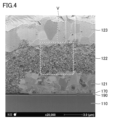
- FIG. 4 is a photograph of an enlarged longitudinal section of a reference electrode of an electrode substrate according to an embodiment of the present invention taken with a scanning electron microscope.
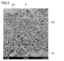
- FIG. 5 is a photograph obtained by further enlarging the V portion of FIG. 4 .
- an SiO 2 film 190 is formed on the surface of an insulating substrate 110 , and a metal wiring layer 170 is formed on the SiO 2 film 190 .
- a silver layer 121 , a first silver chloride layer 122 and a second silver chloride layer 123 are laminated in this order on the metal wiring layer 170 .
- the silver layer 121 is made of polycrystal.
- the first silver chloride layer 122 is formed of a porous material containing many small crystallites and voids.
- the area porosity of the first silver chloride layer 122 is 10% or more.
- the area porosity of the first silver chloride layer 122 derived using the image analysis software "Azo-kun" (registered trademark) manufactured by Asahi Kasei Engineering was 13%.
- the second silver chloride layer 123 is made of polycrystal with an average grain size of 1 ⁇ m or more.
- the second silver chloride layer 123 has a dense structure in which large crystallites are combined.
- the areal porosity of the first silver chloride layer 122 is greater than the areal porosity of the second silver chloride layer 123 in any longitudinal cross section.
- the following chemical reaction can be considered as a mechanism for forming the first silver chloride layer 122 and the second silver chloride layer 123.
- silver located on the surface of the plating film is eluted, and silver chloride containing many voids is formed on the surface.
- This portion becomes the first silver chloride layer 122 .
- the silver eluted from the surface portion becomes silver chloride of high concentration near the surface portion and precipitates outside the surface portion.
- This portion becomes the second silver chloride layer 123 .
- the silver plating film becomes a laminated structure of the silver layer 121, the first silver chloride layer 122 and the second silver chloride layer 123 with volume expansion.
- Table 1 summarizes the physical property values of the materials forming the electrode substrate 100.
- the first silver chloride layer contains voids, values of small coefficient of thermal expansion and small Young's modulus were adopted instead of physical property values or evaluation values.
- the thermal stress relaxation effect is exhibited.
- the first silver chloride layer should be smaller than the second silver chloride layer in either the coefficient of thermal expansion or the Young's modulus.
- the reference electrode according to the comparative example in which the second silver chloride layer 123 is also formed in the portion of the first silver chloride layer 122 and the first silver chloride layer 122 is not formed and the reference electrode according to the present embodiment
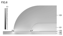
- the results of simulation analysis of the shear stress distribution generated when the temperature of the electrode changes from 20° C. to 100° C. will be described.
- FIG. 6 is a partial vertical cross-sectional view showing the shear stress distribution generated when the temperature is changed from 20° C. to 100° C. in the reference electrode according to the comparative example.
- FIG. 7 is a partial longitudinal sectional view showing the shear stress distribution generated when the temperature is changed from 20° C. to 100° C. in the reference electrode according to this embodiment.
- FIG. 8 is a graph showing changes in shear stress at positions from point A between AA' along the interface between the insulating substrate and the silver chloride layer shown in FIGS.
- the vertical axis indicates the shear stress (MPa)
- the horizontal axis indicates the position ( ⁇ m) from point A between AA'.
- the transition of the reference electrode according to the comparative example is indicated by a dotted line
- the transition of the reference electrode according to the present embodiment is indicated by a solid line.
- the shear stress generated when the temperature changes from 20° C. to 100° C. is lower than in the reference electrode according to the comparative example. .
- the amount of thermal expansion of the first silver chloride layer 122 is small, and the expansion of the second silver chloride layer 123 causes deformation of the first silver chloride layer 122 with a small Young's modulus. This is because the stress concentration at the interface with the layer is alleviated.
- the reference electrode 120 including the first silver chloride layer 122 relieves the stress concentration at the interface between the insulating substrate 110 and the silver chloride layer, and the reference electrode 120 from the insulating substrate 110 It was confirmed that peeling could be suppressed.
- the electrode substrate 100 includes an insulating substrate 110 and a reference electrode 120.
- a reference electrode 120 is formed on the insulating substrate 110 .
- Reference electrode 120 includes silver layer 121 , first silver chloride layer 122 , and second silver chloride layer 123 .
- a silver layer 121 is formed on the insulating substrate 110 .
- the first silver chloride layer 122 is formed over the silver layer 121 and the insulating substrate 110 to cover the silver layer 121 .
- the second silver chloride layer 123 is formed over the first silver chloride layer 122 and the insulating substrate 110 to cover the first silver chloride layer 122 .
- the areal porosity of the first silver chloride layer 122 is greater than the areal porosity of the second silver chloride layer 123 in any longitudinal section. Thereby, peeling of the reference electrode 120 from the insulating substrate 110 can be suppressed.
- the area porosity of the first silver chloride layer 122 is 10% or more.
- stress concentration at the interface between the insulating substrate 110 and the silver chloride layer can be alleviated by the deformation of the first silver chloride layer 122 while reducing the amount of thermal expansion of the first silver chloride layer 122 when the temperature changes. can.
- the ratio of the thickness of the first silver chloride layer 122 to the total value of the thickness of the first silver chloride layer 122 and the thickness of the second silver chloride layer 123 is 20%. That's it. Thereby, the stress relieving effect of the first silver chloride layer 122 can be sufficiently ensured.
- the sum of the thickness of the first silver chloride layer 122 and the thickness of the second silver chloride layer 123 is 20 ⁇ m or less. This can reduce the magnitude of shear stress generated at the interface between the insulating substrate 110 and the silver chloride layer when the temperature changes.
- the second silver chloride layer 123 is made of polycrystal with an average grain size of 1 ⁇ m or more. This allows the reference electrode 120 to be robust as a bulk body.
- the electrode substrate 100 further includes a metal wiring layer 170 formed on the insulating substrate 110 , and the silver layer 121 is formed over the insulating substrate 110 from the metal wiring layer 170 . It covers at least part of the metal wiring layer 170 . As a result, the silver layer 121 can be adhered to the insulating substrate 110 via the metal wiring layer 170 .
- the silver layer 121 is made of polycrystal. This allows the silver layer 121 to be robust as a bulk body.
- the silver layer 121 is a plated film. As a result, the silver layer 121 can be adhered to the insulating substrate 110 via the metal wiring layer 170 .
- the silver layer 121 only partially covers the metal wiring layer 170 .
- a pair of electrodes formed on the insulating substrate 110 is configured by a portion of the metal wiring layer 170 not covered with the silver layer 121 .
- the reference electrode 120 and a pair of electrodes, the first electrode 130 and the second electrode 140 can be integrated on the insulating substrate 110.
- a pair of electrodes are joined to a semiconductor channel formed in an insulating substrate 110.
- the reference electrode 120 and the sensor section including the semiconductor channel can be integrated on the insulating substrate 110 .
- the reference electrode 120 and the sensor portion including the semiconductor channel are integrated on the insulating substrate 110, and the counter electrode or other elements are further integrated on the same insulating substrate 110. It may be integrated.
- Electrode substrate 110 insulating substrate, 120 reference electrode, 121 silver layer, 122 first silver chloride layer, 123 second silver chloride layer, 130 first electrode, 140 second electrode, 150 transmission line, 162 first connection terminal, 163 second connection terminal, 164 third connection terminal, 170 metal wiring layer, 180 electrolytic solution, 190 SiO 2 film.
Landscapes
- Chemical & Material Sciences (AREA)
- Life Sciences & Earth Sciences (AREA)
- Health & Medical Sciences (AREA)
- Biochemistry (AREA)
- General Physics & Mathematics (AREA)
- Electrochemistry (AREA)
- Physics & Mathematics (AREA)
- Analytical Chemistry (AREA)
- Molecular Biology (AREA)
- General Health & Medical Sciences (AREA)
- Chemical Kinetics & Catalysis (AREA)
- Immunology (AREA)
- Pathology (AREA)
- Engineering & Computer Science (AREA)
- Microelectronics & Electronic Packaging (AREA)
- Parts Printed On Printed Circuit Boards (AREA)
- Electrodes Of Semiconductors (AREA)
Priority Applications (3)
| Application Number | Priority Date | Filing Date | Title |
|---|---|---|---|
| JP2023564889A JP7643589B2 (ja) | 2021-12-03 | 2022-11-18 | 電極基板 |
| CN202280079574.5A CN118355269A (zh) | 2021-12-03 | 2022-11-18 | 电极基板 |
| US18/678,044 US20240328985A1 (en) | 2021-12-03 | 2024-05-30 | Electrode substrate |
Applications Claiming Priority (2)
| Application Number | Priority Date | Filing Date | Title |
|---|---|---|---|
| JP2021-196855 | 2021-12-03 | ||
| JP2021196855 | 2021-12-03 |
Related Child Applications (1)
| Application Number | Title | Priority Date | Filing Date |
|---|---|---|---|
| US18/678,044 Continuation US20240328985A1 (en) | 2021-12-03 | 2024-05-30 | Electrode substrate |
Publications (1)
| Publication Number | Publication Date |
|---|---|
| WO2023100694A1 true WO2023100694A1 (ja) | 2023-06-08 |
Family
ID=86612130
Family Applications (1)
| Application Number | Title | Priority Date | Filing Date |
|---|---|---|---|
| PCT/JP2022/042877 Ceased WO2023100694A1 (ja) | 2021-12-03 | 2022-11-18 | 電極基板 |
Country Status (4)
| Country | Link |
|---|---|
| US (1) | US20240328985A1 (cg-RX-API-DMAC7.html) |
| JP (1) | JP7643589B2 (cg-RX-API-DMAC7.html) |
| CN (1) | CN118355269A (cg-RX-API-DMAC7.html) |
| WO (1) | WO2023100694A1 (cg-RX-API-DMAC7.html) |
Citations (3)
| Publication number | Priority date | Publication date | Assignee | Title |
|---|---|---|---|---|
| US4280889A (en) * | 1976-03-11 | 1981-07-28 | Honeywell Inc. | Solid state ion responsive and reference electrodes |
| JPH10253573A (ja) * | 1997-03-11 | 1998-09-25 | Fuji Elelctrochem Co Ltd | 銀・塩化銀参照電極およびその製造方法 |
| CN112255286A (zh) * | 2020-08-11 | 2021-01-22 | 江苏大学 | 一种集成仿生的栽培基质离子浓度在线检测装置及方法 |
-
2022
- 2022-11-18 JP JP2023564889A patent/JP7643589B2/ja active Active
- 2022-11-18 CN CN202280079574.5A patent/CN118355269A/zh not_active Withdrawn
- 2022-11-18 WO PCT/JP2022/042877 patent/WO2023100694A1/ja not_active Ceased
-
2024
- 2024-05-30 US US18/678,044 patent/US20240328985A1/en not_active Abandoned
Patent Citations (3)
| Publication number | Priority date | Publication date | Assignee | Title |
|---|---|---|---|---|
| US4280889A (en) * | 1976-03-11 | 1981-07-28 | Honeywell Inc. | Solid state ion responsive and reference electrodes |
| JPH10253573A (ja) * | 1997-03-11 | 1998-09-25 | Fuji Elelctrochem Co Ltd | 銀・塩化銀参照電極およびその製造方法 |
| CN112255286A (zh) * | 2020-08-11 | 2021-01-22 | 江苏大学 | 一种集成仿生的栽培基质离子浓度在线检测装置及方法 |
Also Published As
| Publication number | Publication date |
|---|---|
| CN118355269A (zh) | 2024-07-16 |
| JPWO2023100694A1 (cg-RX-API-DMAC7.html) | 2023-06-08 |
| US20240328985A1 (en) | 2024-10-03 |
| JP7643589B2 (ja) | 2025-03-11 |
Similar Documents
| Publication | Publication Date | Title |
|---|---|---|
| Park et al. | New Approach for large-area thermoelectric junctions with a liquid eutectic gallium–indium electrode | |
| Liu et al. | van der Waals contact engineering of graphene field-effect transistors for large-area flexible electronics | |
| Akkerman et al. | Electron tunneling through alkanedithiol self-assembled monolayers in large-area molecular junctions | |
| US8168534B2 (en) | Methods of fabricating electrodes and uses thereof | |
| US9601697B2 (en) | Systems and process for forming carbon nanotube sensors | |
| JP6719581B2 (ja) | グラフェン薄膜トランジスタの製造方法 | |
| TW584934B (en) | Method of forming a contact and structure thereof | |
| US10790335B2 (en) | Method for making three dimensional complementary metal oxide semiconductor carbon nanotube thin film transistor circuit | |
| WO2009104769A1 (ja) | タッチパネルセンサー | |
| CN104919540B (zh) | 导电体及其制造方法 | |
| JPWO2009013876A1 (ja) | 電気化学測定用電極板、およびこの電極板を有する電気化学測定装置、ならびにこの電極板を用いて目的物質を定量する方法 | |
| CN110879464A (zh) | 电润湿装置 | |
| US10976852B2 (en) | Touch panel, manufacturing method thereof, and display device | |
| TW201519445A (zh) | 有機無機混合型電晶體 | |
| Ahmed et al. | Development of EGFET-based ITO pH sensors using epoxy free membrane | |
| US20180219044A1 (en) | Three dimensional complementary metal oxide semiconductor carbon nanotube thin film transistor circuit | |
| Sahalov et al. | Influence of applied potential on the impedance of alkanethiol SAMs | |
| CN105917482A (zh) | 用于晶体管装置的源极/漏极导体 | |
| JP7643589B2 (ja) | 電極基板 | |
| TWI283766B (en) | Thin film transistor substrate and method of manufacturing the same | |
| WO2020000897A1 (zh) | 触控面板及其制作方法、显示装置 | |
| JP4982899B2 (ja) | 微小電極およびその製造方法 | |
| Vinod et al. | Nonplanar conductive surfaces via “Bottom-Up” nanostructured gold coating | |
| Nishimura et al. | Effects of Surface Oxygen Vacancies and Hydroxy Groups on Electrical Characteristics in Solution-Gated One-Piece Indium–Tin-Oxide-Based Field-Effect Transistors | |
| JP2006332614A5 (cg-RX-API-DMAC7.html) |
Legal Events
| Date | Code | Title | Description |
|---|---|---|---|
| 121 | Ep: the epo has been informed by wipo that ep was designated in this application |
Ref document number: 22901127 Country of ref document: EP Kind code of ref document: A1 |
|
| ENP | Entry into the national phase |
Ref document number: 2023564889 Country of ref document: JP Kind code of ref document: A |
|
| WWE | Wipo information: entry into national phase |
Ref document number: 202280079574.5 Country of ref document: CN |
|
| NENP | Non-entry into the national phase |
Ref country code: DE |
|
| 122 | Ep: pct application non-entry in european phase |
Ref document number: 22901127 Country of ref document: EP Kind code of ref document: A1 |