WO2023095461A1 - カテコール基を有する薬液耐性保護膜形成用組成物 - Google Patents
カテコール基を有する薬液耐性保護膜形成用組成物 Download PDFInfo
- Publication number
- WO2023095461A1 WO2023095461A1 PCT/JP2022/037533 JP2022037533W WO2023095461A1 WO 2023095461 A1 WO2023095461 A1 WO 2023095461A1 JP 2022037533 W JP2022037533 W JP 2022037533W WO 2023095461 A1 WO2023095461 A1 WO 2023095461A1
- Authority
- WO
- WIPO (PCT)
- Prior art keywords
- group
- protective film
- forming
- composition
- film
- Prior art date
- Legal status (The legal status is an assumption and is not a legal conclusion. Google has not performed a legal analysis and makes no representation as to the accuracy of the status listed.)
- Ceased
Links
Classifications
-
- G—PHYSICS
- G03—PHOTOGRAPHY; CINEMATOGRAPHY; ANALOGOUS TECHNIQUES USING WAVES OTHER THAN OPTICAL WAVES; ELECTROGRAPHY; HOLOGRAPHY
- G03F—PHOTOMECHANICAL PRODUCTION OF TEXTURED OR PATTERNED SURFACES, e.g. FOR PRINTING, FOR PROCESSING OF SEMICONDUCTOR DEVICES; MATERIALS THEREFOR; ORIGINALS THEREFOR; APPARATUS SPECIALLY ADAPTED THEREFOR
- G03F7/00—Photomechanical, e.g. photolithographic, production of textured or patterned surfaces, e.g. printing surfaces; Materials therefor, e.g. comprising photoresists; Apparatus specially adapted therefor
- G03F7/004—Photosensitive materials
- G03F7/09—Photosensitive materials characterised by structural details, e.g. supports, auxiliary layers
- G03F7/11—Photosensitive materials characterised by structural details, e.g. supports, auxiliary layers having cover layers or intermediate layers, e.g. subbing layers
-
- C—CHEMISTRY; METALLURGY
- C07—ORGANIC CHEMISTRY
- C07D—HETEROCYCLIC COMPOUNDS
- C07D251/00—Heterocyclic compounds containing 1,3,5-triazine rings
- C07D251/02—Heterocyclic compounds containing 1,3,5-triazine rings not condensed with other rings
- C07D251/12—Heterocyclic compounds containing 1,3,5-triazine rings not condensed with other rings having three double bonds between ring members or between ring members and non-ring members
- C07D251/26—Heterocyclic compounds containing 1,3,5-triazine rings not condensed with other rings having three double bonds between ring members or between ring members and non-ring members with only hetero atoms directly attached to ring carbon atoms
- C07D251/30—Only oxygen atoms
- C07D251/34—Cyanuric or isocyanuric esters
-
- C—CHEMISTRY; METALLURGY
- C08—ORGANIC MACROMOLECULAR COMPOUNDS; THEIR PREPARATION OR CHEMICAL WORKING-UP; COMPOSITIONS BASED THEREON
- C08F—MACROMOLECULAR COMPOUNDS OBTAINED BY REACTIONS ONLY INVOLVING CARBON-TO-CARBON UNSATURATED BONDS
- C08F20/00—Homopolymers and copolymers of compounds having one or more unsaturated aliphatic radicals, each having only one carbon-to-carbon double bond, and only one being terminated by only one carboxyl radical or a salt, anhydride, ester, amide, imide or nitrile thereof
- C08F20/02—Monocarboxylic acids having less than ten carbon atoms, Derivatives thereof
- C08F20/10—Esters
- C08F20/26—Esters containing oxygen in addition to the carboxy oxygen
- C08F20/28—Esters containing oxygen in addition to the carboxy oxygen containing no aromatic rings in the alcohol moiety
-
- C—CHEMISTRY; METALLURGY
- C08—ORGANIC MACROMOLECULAR COMPOUNDS; THEIR PREPARATION OR CHEMICAL WORKING-UP; COMPOSITIONS BASED THEREON
- C08G—MACROMOLECULAR COMPOUNDS OBTAINED OTHERWISE THAN BY REACTIONS ONLY INVOLVING UNSATURATED CARBON-TO-CARBON BONDS
- C08G59/00—Polycondensates containing more than one epoxy group per molecule; Macromolecules obtained by polymerising compounds containing more than one epoxy group per molecule using curing agents or catalysts which react with the epoxy groups
- C08G59/02—Polycondensates containing more than one epoxy group per molecule
-
- C—CHEMISTRY; METALLURGY
- C08—ORGANIC MACROMOLECULAR COMPOUNDS; THEIR PREPARATION OR CHEMICAL WORKING-UP; COMPOSITIONS BASED THEREON
- C08G—MACROMOLECULAR COMPOUNDS OBTAINED OTHERWISE THAN BY REACTIONS ONLY INVOLVING UNSATURATED CARBON-TO-CARBON BONDS
- C08G59/00—Polycondensates containing more than one epoxy group per molecule; Macromolecules obtained by polymerising compounds containing more than one epoxy group per molecule using curing agents or catalysts which react with the epoxy groups
- C08G59/18—Macromolecules obtained by polymerising compounds containing more than one epoxy group per molecule using curing agents or catalysts which react with the epoxy groups ; e.g. general methods of curing
- C08G59/20—Macromolecules obtained by polymerising compounds containing more than one epoxy group per molecule using curing agents or catalysts which react with the epoxy groups ; e.g. general methods of curing characterised by the epoxy compounds used
- C08G59/32—Epoxy compounds containing three or more epoxy groups
- C08G59/3236—Heterocylic compounds
- C08G59/3245—Heterocylic compounds containing only nitrogen as a heteroatom
-
- C—CHEMISTRY; METALLURGY
- C08—ORGANIC MACROMOLECULAR COMPOUNDS; THEIR PREPARATION OR CHEMICAL WORKING-UP; COMPOSITIONS BASED THEREON
- C08G—MACROMOLECULAR COMPOUNDS OBTAINED OTHERWISE THAN BY REACTIONS ONLY INVOLVING UNSATURATED CARBON-TO-CARBON BONDS
- C08G59/00—Polycondensates containing more than one epoxy group per molecule; Macromolecules obtained by polymerising compounds containing more than one epoxy group per molecule using curing agents or catalysts which react with the epoxy groups
- C08G59/18—Macromolecules obtained by polymerising compounds containing more than one epoxy group per molecule using curing agents or catalysts which react with the epoxy groups ; e.g. general methods of curing
- C08G59/40—Macromolecules obtained by polymerising compounds containing more than one epoxy group per molecule using curing agents or catalysts which react with the epoxy groups ; e.g. general methods of curing characterised by the curing agents used
- C08G59/4007—Curing agents not provided for by the groups C08G59/42 - C08G59/66
- C08G59/4014—Nitrogen containing compounds
-
- C—CHEMISTRY; METALLURGY
- C08—ORGANIC MACROMOLECULAR COMPOUNDS; THEIR PREPARATION OR CHEMICAL WORKING-UP; COMPOSITIONS BASED THEREON
- C08G—MACROMOLECULAR COMPOUNDS OBTAINED OTHERWISE THAN BY REACTIONS ONLY INVOLVING UNSATURATED CARBON-TO-CARBON BONDS
- C08G59/00—Polycondensates containing more than one epoxy group per molecule; Macromolecules obtained by polymerising compounds containing more than one epoxy group per molecule using curing agents or catalysts which react with the epoxy groups
- C08G59/18—Macromolecules obtained by polymerising compounds containing more than one epoxy group per molecule using curing agents or catalysts which react with the epoxy groups ; e.g. general methods of curing
- C08G59/68—Macromolecules obtained by polymerising compounds containing more than one epoxy group per molecule using curing agents or catalysts which react with the epoxy groups ; e.g. general methods of curing characterised by the catalysts used
- C08G59/687—Macromolecules obtained by polymerising compounds containing more than one epoxy group per molecule using curing agents or catalysts which react with the epoxy groups ; e.g. general methods of curing characterised by the catalysts used containing sulfur
-
- C—CHEMISTRY; METALLURGY
- C09—DYES; PAINTS; POLISHES; NATURAL RESINS; ADHESIVES; COMPOSITIONS NOT OTHERWISE PROVIDED FOR; APPLICATIONS OF MATERIALS NOT OTHERWISE PROVIDED FOR
- C09D—COATING COMPOSITIONS, e.g. PAINTS, VARNISHES OR LACQUERS; FILLING PASTES; CHEMICAL PAINT OR INK REMOVERS; INKS; CORRECTING FLUIDS; WOODSTAINS; PASTES OR SOLIDS FOR COLOURING OR PRINTING; USE OF MATERIALS THEREFOR
- C09D163/00—Coating compositions based on epoxy resins; Coating compositions based on derivatives of epoxy resins
-
- G—PHYSICS
- G03—PHOTOGRAPHY; CINEMATOGRAPHY; ANALOGOUS TECHNIQUES USING WAVES OTHER THAN OPTICAL WAVES; ELECTROGRAPHY; HOLOGRAPHY
- G03F—PHOTOMECHANICAL PRODUCTION OF TEXTURED OR PATTERNED SURFACES, e.g. FOR PRINTING, FOR PROCESSING OF SEMICONDUCTOR DEVICES; MATERIALS THEREFOR; ORIGINALS THEREFOR; APPARATUS SPECIALLY ADAPTED THEREFOR
- G03F7/00—Photomechanical, e.g. photolithographic, production of textured or patterned surfaces, e.g. printing surfaces; Materials therefor, e.g. comprising photoresists; Apparatus specially adapted therefor
- G03F7/004—Photosensitive materials
- G03F7/09—Photosensitive materials characterised by structural details, e.g. supports, auxiliary layers
- G03F7/094—Multilayer resist systems, e.g. planarising layers
-
- G—PHYSICS
- G03—PHOTOGRAPHY; CINEMATOGRAPHY; ANALOGOUS TECHNIQUES USING WAVES OTHER THAN OPTICAL WAVES; ELECTROGRAPHY; HOLOGRAPHY
- G03F—PHOTOMECHANICAL PRODUCTION OF TEXTURED OR PATTERNED SURFACES, e.g. FOR PRINTING, FOR PROCESSING OF SEMICONDUCTOR DEVICES; MATERIALS THEREFOR; ORIGINALS THEREFOR; APPARATUS SPECIALLY ADAPTED THEREFOR
- G03F7/00—Photomechanical, e.g. photolithographic, production of textured or patterned surfaces, e.g. printing surfaces; Materials therefor, e.g. comprising photoresists; Apparatus specially adapted therefor
- G03F7/16—Coating processes; Apparatus therefor
- G03F7/168—Finishing the coated layer, e.g. drying, baking, soaking
-
- H—ELECTRICITY
- H10—SEMICONDUCTOR DEVICES; ELECTRIC SOLID-STATE DEVICES NOT OTHERWISE PROVIDED FOR
- H10P—GENERIC PROCESSES OR APPARATUS FOR THE MANUFACTURE OR TREATMENT OF DEVICES COVERED BY CLASS H10
- H10P50/00—Etching of wafers, substrates or parts of devices
- H10P50/69—Etching of wafers, substrates or parts of devices using masks for semiconductor materials
- H10P50/691—Etching of wafers, substrates or parts of devices using masks for semiconductor materials for Group V materials or Group III-V materials
- H10P50/692—Etching of wafers, substrates or parts of devices using masks for semiconductor materials for Group V materials or Group III-V materials characterised by their composition, e.g. multilayer masks or materials
-
- H—ELECTRICITY
- H10—SEMICONDUCTOR DEVICES; ELECTRIC SOLID-STATE DEVICES NOT OTHERWISE PROVIDED FOR
- H10P—GENERIC PROCESSES OR APPARATUS FOR THE MANUFACTURE OR TREATMENT OF DEVICES COVERED BY CLASS H10
- H10P50/00—Etching of wafers, substrates or parts of devices
- H10P50/69—Etching of wafers, substrates or parts of devices using masks for semiconductor materials
- H10P50/691—Etching of wafers, substrates or parts of devices using masks for semiconductor materials for Group V materials or Group III-V materials
- H10P50/693—Etching of wafers, substrates or parts of devices using masks for semiconductor materials for Group V materials or Group III-V materials characterised by their size, orientation, disposition, behaviour or shape, in horizontal or vertical plane
- H10P50/695—Etching of wafers, substrates or parts of devices using masks for semiconductor materials for Group V materials or Group III-V materials characterised by their size, orientation, disposition, behaviour or shape, in horizontal or vertical plane characterised by the process involved to create the mask, e.g. lift-off masks or sidewalls or to modify the mask
-
- H—ELECTRICITY
- H10—SEMICONDUCTOR DEVICES; ELECTRIC SOLID-STATE DEVICES NOT OTHERWISE PROVIDED FOR
- H10P—GENERIC PROCESSES OR APPARATUS FOR THE MANUFACTURE OR TREATMENT OF DEVICES COVERED BY CLASS H10
- H10P50/00—Etching of wafers, substrates or parts of devices
- H10P50/71—Etching of wafers, substrates or parts of devices using masks for conductive or resistive materials
-
- H—ELECTRICITY
- H10—SEMICONDUCTOR DEVICES; ELECTRIC SOLID-STATE DEVICES NOT OTHERWISE PROVIDED FOR
- H10P—GENERIC PROCESSES OR APPARATUS FOR THE MANUFACTURE OR TREATMENT OF DEVICES COVERED BY CLASS H10
- H10P50/00—Etching of wafers, substrates or parts of devices
- H10P50/73—Etching of wafers, substrates or parts of devices using masks for insulating materials
-
- H—ELECTRICITY
- H10—SEMICONDUCTOR DEVICES; ELECTRIC SOLID-STATE DEVICES NOT OTHERWISE PROVIDED FOR
- H10P—GENERIC PROCESSES OR APPARATUS FOR THE MANUFACTURE OR TREATMENT OF DEVICES COVERED BY CLASS H10
- H10P76/00—Manufacture or treatment of masks on semiconductor bodies, e.g. by lithography or photolithography
-
- H—ELECTRICITY
- H10—SEMICONDUCTOR DEVICES; ELECTRIC SOLID-STATE DEVICES NOT OTHERWISE PROVIDED FOR
- H10P—GENERIC PROCESSES OR APPARATUS FOR THE MANUFACTURE OR TREATMENT OF DEVICES COVERED BY CLASS H10
- H10P76/00—Manufacture or treatment of masks on semiconductor bodies, e.g. by lithography or photolithography
- H10P76/20—Manufacture or treatment of masks on semiconductor bodies, e.g. by lithography or photolithography of masks comprising organic materials
- H10P76/204—Manufacture or treatment of masks on semiconductor bodies, e.g. by lithography or photolithography of masks comprising organic materials of organic photoresist masks
- H10P76/2041—Photolithographic processes
- H10P76/2042—Photolithographic processes using lasers
-
- C—CHEMISTRY; METALLURGY
- C08—ORGANIC MACROMOLECULAR COMPOUNDS; THEIR PREPARATION OR CHEMICAL WORKING-UP; COMPOSITIONS BASED THEREON
- C08G—MACROMOLECULAR COMPOUNDS OBTAINED OTHERWISE THAN BY REACTIONS ONLY INVOLVING UNSATURATED CARBON-TO-CARBON BONDS
- C08G2150/00—Compositions for coatings
-
- C—CHEMISTRY; METALLURGY
- C09—DYES; PAINTS; POLISHES; NATURAL RESINS; ADHESIVES; COMPOSITIONS NOT OTHERWISE PROVIDED FOR; APPLICATIONS OF MATERIALS NOT OTHERWISE PROVIDED FOR
- C09D—COATING COMPOSITIONS, e.g. PAINTS, VARNISHES OR LACQUERS; FILLING PASTES; CHEMICAL PAINT OR INK REMOVERS; INKS; CORRECTING FLUIDS; WOODSTAINS; PASTES OR SOLIDS FOR COLOURING OR PRINTING; USE OF MATERIALS THEREFOR
- C09D7/00—Features of coating compositions, not provided for in group C09D5/00; Processes for incorporating ingredients in coating compositions
- C09D7/20—Diluents or solvents
-
- H—ELECTRICITY
- H10—SEMICONDUCTOR DEVICES; ELECTRIC SOLID-STATE DEVICES NOT OTHERWISE PROVIDED FOR
- H10P—GENERIC PROCESSES OR APPARATUS FOR THE MANUFACTURE OR TREATMENT OF DEVICES COVERED BY CLASS H10
- H10P50/00—Etching of wafers, substrates or parts of devices
- H10P50/20—Dry etching; Plasma etching; Reactive-ion etching
- H10P50/28—Dry etching; Plasma etching; Reactive-ion etching of insulating materials
- H10P50/282—Dry etching; Plasma etching; Reactive-ion etching of insulating materials of inorganic materials
- H10P50/283—Dry etching; Plasma etching; Reactive-ion etching of insulating materials of inorganic materials by chemical means
-
- H—ELECTRICITY
- H10—SEMICONDUCTOR DEVICES; ELECTRIC SOLID-STATE DEVICES NOT OTHERWISE PROVIDED FOR
- H10P—GENERIC PROCESSES OR APPARATUS FOR THE MANUFACTURE OR TREATMENT OF DEVICES COVERED BY CLASS H10
- H10P50/00—Etching of wafers, substrates or parts of devices
- H10P50/60—Wet etching
- H10P50/64—Wet etching of semiconductor materials
- H10P50/642—Chemical etching
- H10P50/646—Chemical etching of Group III-V materials
-
- H—ELECTRICITY
- H10—SEMICONDUCTOR DEVICES; ELECTRIC SOLID-STATE DEVICES NOT OTHERWISE PROVIDED FOR
- H10P—GENERIC PROCESSES OR APPARATUS FOR THE MANUFACTURE OR TREATMENT OF DEVICES COVERED BY CLASS H10
- H10P50/00—Etching of wafers, substrates or parts of devices
- H10P50/60—Wet etching
- H10P50/66—Wet etching of conductive or resistive materials
- H10P50/663—Wet etching of conductive or resistive materials by chemical means only
- H10P50/667—Wet etching of conductive or resistive materials by chemical means only by liquid etching only
-
- H—ELECTRICITY
- H10—SEMICONDUCTOR DEVICES; ELECTRIC SOLID-STATE DEVICES NOT OTHERWISE PROVIDED FOR
- H10P—GENERIC PROCESSES OR APPARATUS FOR THE MANUFACTURE OR TREATMENT OF DEVICES COVERED BY CLASS H10
- H10P70/00—Cleaning of wafers, substrates or parts of devices
- H10P70/20—Cleaning during device manufacture
- H10P70/23—Cleaning during device manufacture during, before or after processing of insulating materials
-
- H—ELECTRICITY
- H10—SEMICONDUCTOR DEVICES; ELECTRIC SOLID-STATE DEVICES NOT OTHERWISE PROVIDED FOR
- H10P—GENERIC PROCESSES OR APPARATUS FOR THE MANUFACTURE OR TREATMENT OF DEVICES COVERED BY CLASS H10
- H10P70/00—Cleaning of wafers, substrates or parts of devices
- H10P70/20—Cleaning during device manufacture
- H10P70/27—Cleaning during device manufacture during, before or after processing of conductive materials, e.g. polysilicon or amorphous silicon layers
Definitions
- the present invention relates to a composition for forming a protective film that is particularly resistant to wet etching solutions for semiconductors in the lithographic process of semiconductor manufacturing.
- the present invention also relates to a protective film formed from the composition, a method for manufacturing a substrate with a resist pattern to which the protective film is applied, and a method for manufacturing a semiconductor device.
- Patent Document 1 discloses a resist underlayer film material having resistance to alkaline hydrogen peroxide water.
- the protective film on a semiconductor substrate is formed using a protective film-forming composition, and the underlying substrate is processed by wet etching using the protective film as an etching mask, the protective film has a good mask function ( That is, the masked portion can protect the substrate).
- composition for forming a protective film that has good coverage even on a so-called stepped substrate, has a small film thickness difference after embedding, and is capable of forming a flat film.
- the protective film used for the above purpose is expected to function as a so-called resist underlayer film, and is desired to exhibit excellent resistance to resist solvents.
- the present invention has been made in view of the above circumstances, and is a protective film capable of forming a protective film having excellent resistance to semiconductor wet etching solutions such as basic hydrogen peroxide solution and acidic hydrogen peroxide solution.
- An object of the present invention is to provide a film-forming composition which exhibits excellent resistance to resist solvents and can be effectively used as a composition for forming a resist underlayer film.
- a film obtained from a composition for forming a protective film containing a compound represented by a specific structural formula having a catechol group is a wet film for semiconductors.
- the present invention was completed based on the finding that it exhibits excellent resistance to etching solutions.
- X is an n-valent organic group represented by the following formula (A-2), [1 ]
- C a cross-linking agent
- D a cross-linking catalyst
- E a surfactant
- a composition for forming a protective film of [4] The protective film-forming composition further contains (F) a compound or polymer containing a (meth)acryloyl group, a styrene group, a phenolic hydroxy group, an ether group, an epoxy group, or an oxetanyl group. , The composition for forming a protective film according to any one of [1] to [3]. [5] The composition for forming a protective film according to [4], further comprising (G) a polymer having a repeating structural unit represented by the following formula (G).
- R 101 represents a hydrogen atom or a methyl group
- R 102 represents a group selected from the following formulas (g-1) to (g-3), a carbon which may be interrupted by oxygen, represents an alkyl group having 1 to 4 atoms, an optionally substituted aryl group, or a hydroxy group
- R 103 represents an alkylene group having 1 to 4 carbon atoms
- n represents 0 or 1
- the composition for forming a protective film further contains a compound (J) or a polymer (J) containing (J) a cyclic ether having a three-membered ring structure or a four-membered ring structure, [4] The composition for forming a protective film according to .
- a protective film against a wet etching solution for semiconductors which is a baked product of a coating film made of the composition for forming a protective film according to any one of [1] to [6].
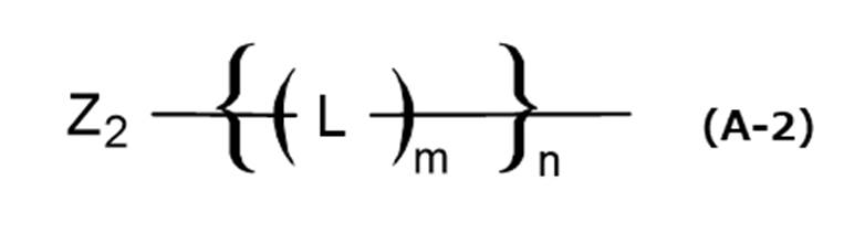
- X when X is a non-divalent n-valent organic group having 2 to 50 carbon atoms, X is an n-valent organic group represented by the following formula (A-2), [8 ] and the composition for forming a resist underlayer film.
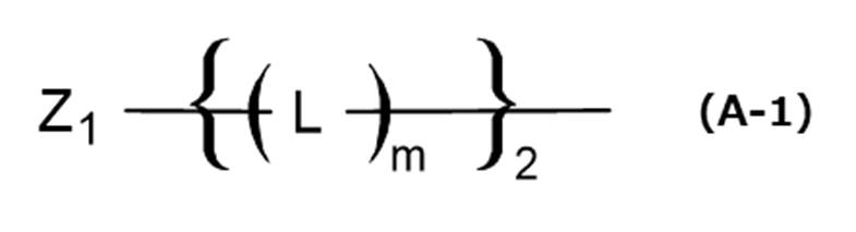
- Z 1 is an alkylene group having 1 to 6 carbon atoms, an optionally substituted aromatic ring, an optionally substituted aliphatic ring, and a substituted m represents 0 or 1
- a resist underlayer film characterized by being a baked product of a coating film made of the composition for forming a resist underlayer film according to [8] or [9].
- [11] Used for manufacturing a semiconductor including a step of applying the protective film-forming composition according to any one of [1] to [6] onto a semiconductor substrate having steps and baking the composition to form a protective film.
- a method for manufacturing a substrate with a protective film characterized by: [12] The composition for forming a protective film according to any one of [1] to [6] or the composition for forming a resist underlayer film according to [8] or [9] is coated on a semiconductor substrate and baked. forming a protective film as a resist underlayer film; forming a resist film on the protective film; and then exposing and developing the resist to form a resist pattern.
- a method for manufacturing a patterned substrate characterized by: [12] The composition for forming a protective film according to any one of [1] to [6] or the composition for forming a resist underlayer film according to [8] or [9] is coated on a semiconductor substrate and baked. forming a protective film as a resist underlayer film; forming a resist film
- a protective film on a semiconductor substrate which may have an inorganic film formed on its surface using the protective film-forming composition according to any one of [1] to [6], forming a resist pattern thereon, dry-etching the protective film using the resist pattern as a mask, exposing the surface of the inorganic film or the semiconductor substrate, and using the dry-etched protective film as a mask for semiconductor wet etching.
- a method of manufacturing a semiconductor device comprising the steps of wet etching and cleaning the inorganic film or the semiconductor substrate using a liquid.
- a resist underlayer film is formed on a semiconductor substrate which may have an inorganic film formed thereon using the composition for forming a resist underlayer film according to [8] or [9], and the resist underlayer film is formed. forming a resist pattern thereon, dry-etching the resist underlayer film using the resist pattern as a mask to expose the surface of the inorganic film or the semiconductor substrate, and using the resist underlayer film after dry etching as a mask; A method of manufacturing a semiconductor device, comprising the step of etching the film or the semiconductor substrate.
- a composition for forming a protective film capable of forming a protective film having excellent resistance to semiconductor wet etching solutions such as basic hydrogen peroxide solution and acidic hydrogen peroxide solution, comprising: It is also possible to provide a composition that exhibits excellent resistance to and can be effectively used as a composition for forming a resist underlayer film.
- the composition for forming a protective film of the present invention is required to have, for example, the following properties in a well-balanced manner in the lithography process in the manufacture of semiconductors.
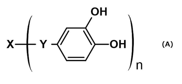
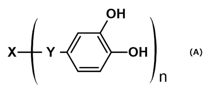
- composition for forming protective film against wet etching solution for semiconductors is (A) a compound represented by the following formula (A); and (B) a solvent.
- the protective film-forming composition of the present invention includes (A) a compound represented by the following formula (A) and (B) a solvent, as well as (C) a cross-linking agent, (D) a cross-linking catalyst, and (E) a surfactant. At least one of the agents may be contained.
- the composition for forming a protective film of the present invention contains (F) a (meth)acryloyl group, a styrene group, a phenolic hydroxy compounds or polymers containing groups, ether groups, epoxy groups, or oxetanyl groups.
- composition for forming a protective film against a wet etching solution for semiconductors of the present invention contains (A) a compound represented by the following formula (A).
- n represents an integer of 1 to 10, and when n is 2, X represents a sulfinyl group, a sulfonyl group, an ether group, or a divalent organic group having 2 to 50 carbon atoms, n When is an integer other than 2, X represents an n-valent organic group having 2 to 50 carbon atoms.
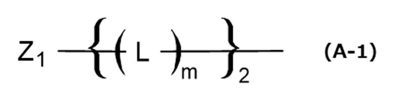
- X when X is a divalent organic group having 2 to 50 carbon atoms, X is a divalent organic group represented by the following formula (A-1), and X is a carbon atom In the case of an n-valent organic group other than divalent number 2 to 50, X is an n-valent organic group represented by the following formula (A-2).
- an optionally substituted aromatic ring an optionally substituted aliphatic ring, or an optionally substituted heterocyclic ring
- the substituent referred to in is an alkyl group having 1 to 10 carbon atoms which may be interrupted by an oxygen atom or a sulfur atom, an alkenyl group having 1 to 10 carbon atoms which may be interrupted by an oxygen atom or a sulfur atom, or It represents an alkynyl group having 1 to 10 carbon atoms which may be interrupted by an oxygen atom or a sulfur atom.
- the alkyl group, alkenyl group, and alkynyl group may be linear or branched.
- the alkylene group refers to a divalent group derived by removing one more hydrogen atom from an alkyl group. It may be linear or branched.
- aromatic rings in the formulas (A-1) and (A-2) include benzene, naphthalene, anthracene, acenaphthene, fluorene, triphenylene, phenalene, phenanthrene, indene, indane, indacene, and pyrene. , chrysene, perylene, naphthacene, pentacene, coronene, heptacene, benzo[a]anthracene, dibenzophenanthrene and dibenzo[a,j]anthracene.
- heterocyclic ring in the formulas (A-1) and (A-2) include furan, thiophene, pyrrole, imidazole, pyran, pyridine, pyrimidine, pyrazine, pyrrolidine, piperidine, piperazine, morpholine, quinuclidine, indole, purine, thymine, quinoline, isoquinoline, chromene, thianthrene, phenothiazine, phenoxazine, xanthene, acridine, phenazine, carbazole, hydantoin, uracil, barbituric acid, triazine, cyanuric acid and the like.
- a heterocycle may be a triazinetrione.
- alkyl groups having 1 to 10 carbon atoms include methyl group, ethyl group, n-propyl group, i-propyl group, cyclopropyl group, n-butyl group, i-butyl group, s-butyl group and t-butyl group, cyclobutyl group, 1-methyl-cyclopropyl group, 2-methyl-cyclopropyl group, n-pentyl group, 1-methyl-n-butyl group, 2-methyl-n-butyl group, 3-methyl-n- butyl group, 1,1-dimethyl-n-propyl group, 1,2-dimethyl-n-propyl group, 2,2-dimethyl-n-propyl group, 1-ethyl-n-propyl group, cyclopentyl group, 1- methyl-cyclobutyl group, 2-methyl-cyclobutyl group, 3-methyl-cyclobutyl group, 1,2-dimethyl-cyclopropyl group, 2,2-
- Optionally interrupted means that any carbon-carbon atom in an alkyl group, alkenyl group, or alkynyl group is a heteroatom (that is, an ether bond in the case of oxygen, a sulfide bond in the case of sulfur) say that it is interrupted by
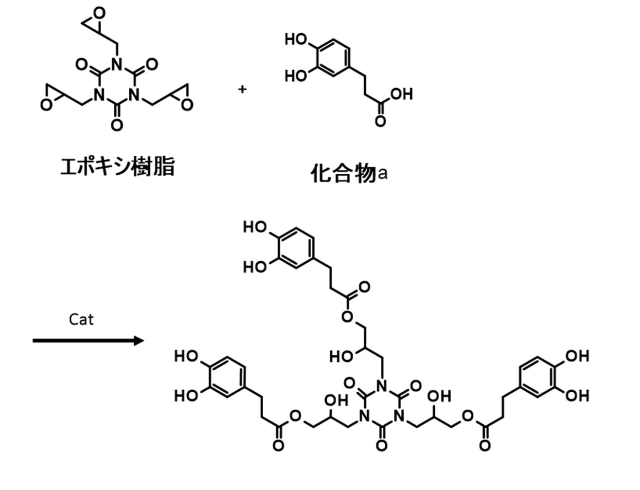
- a reaction for obtaining a compound represented by formula (A) using triazinetrione as an epoxy resin and t in Y being 1 is shown below.
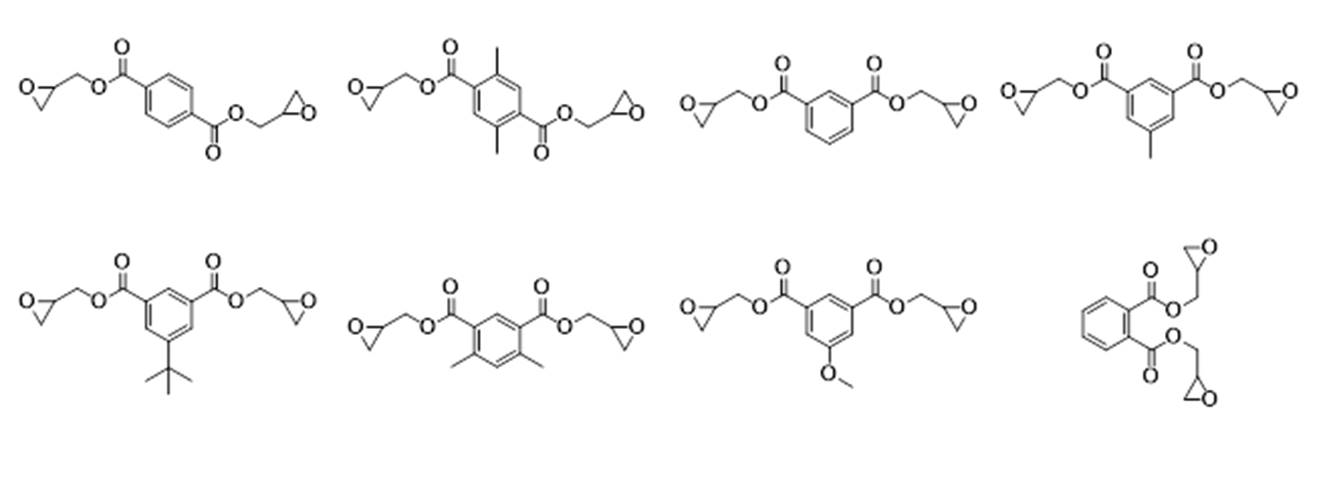
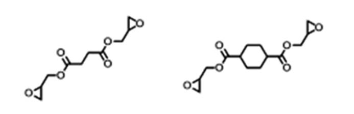
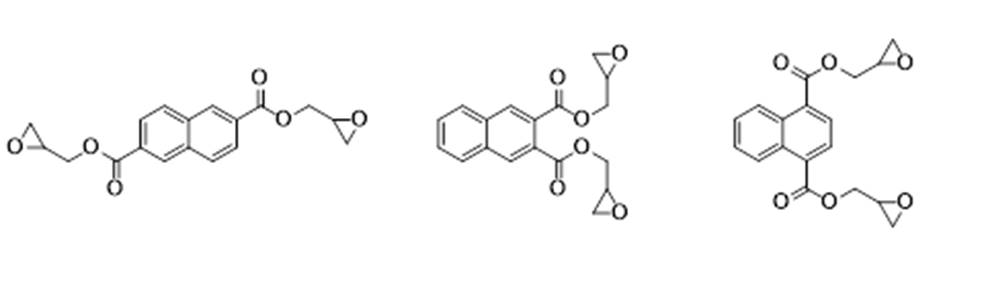
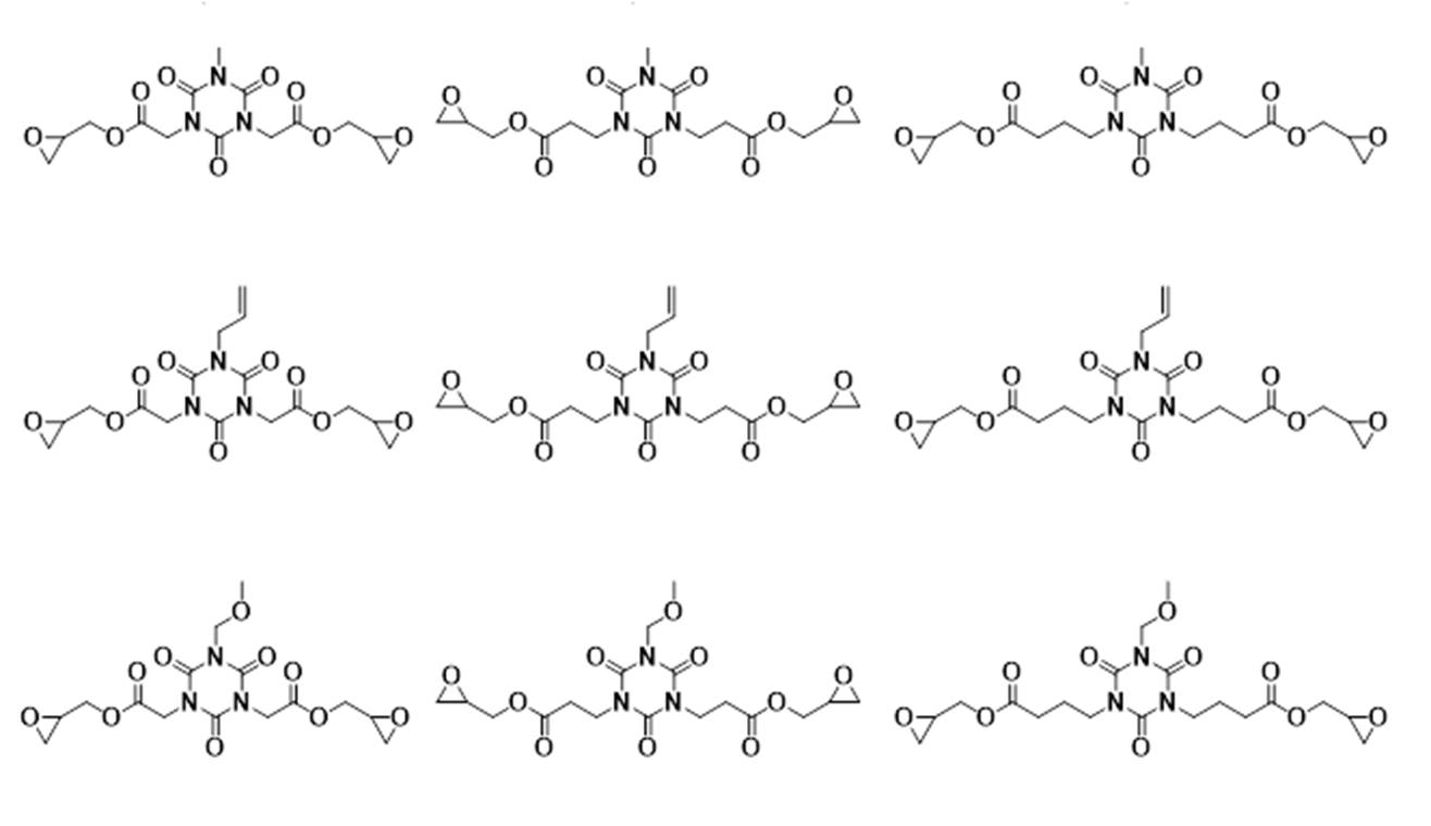
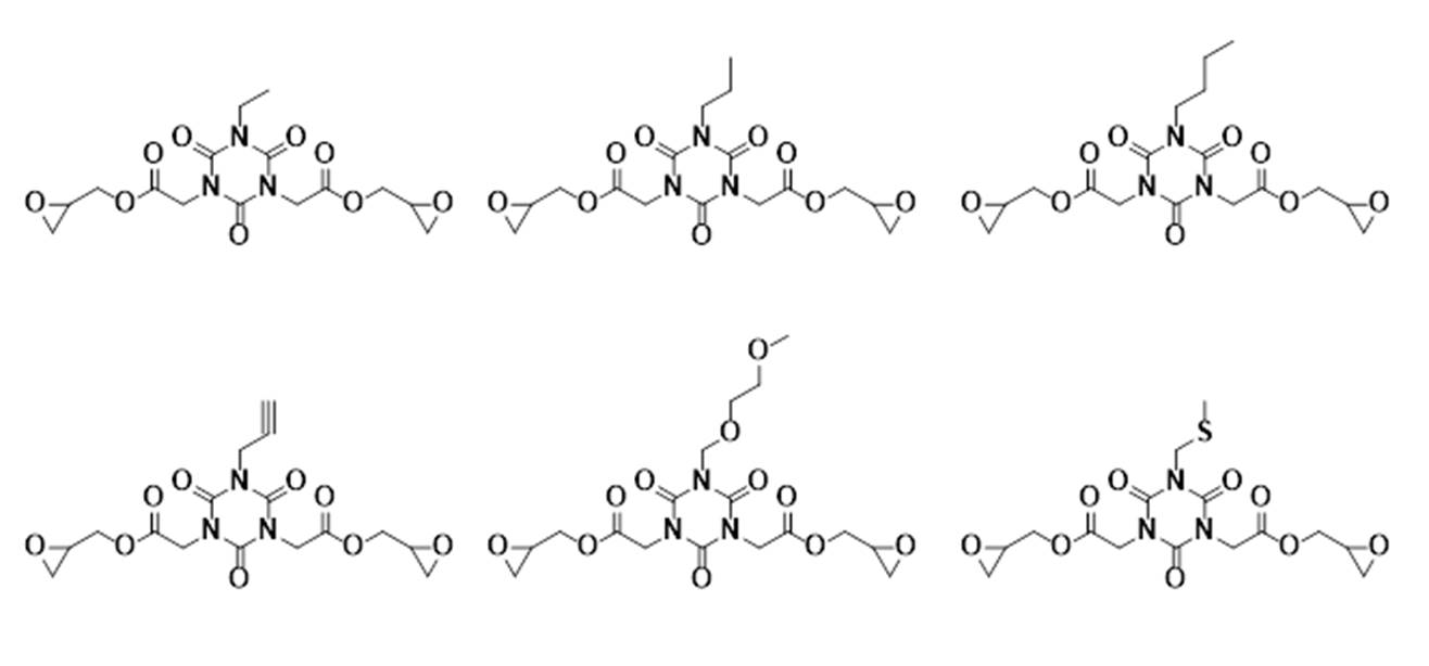
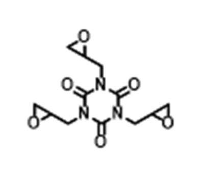
- epoxy resin used to obtain the compound represented by the above formula (A) include, for example, the epoxy resins represented below.
- composition for forming a protective film of the present invention can be prepared by dissolving each component described above in a solvent, preferably an organic solvent, and used in a uniform solution state.
- any organic solvent capable of dissolving the above compound (A) and other optional solid components such as solid components can be used without particular limitation.
- the composition for forming a protective film according to the present invention is used in the form of a uniform solution, it is recommended to use an organic solvent commonly used in lithography processes in combination, considering its coating performance. be.
- organic solvents examples include ethylene glycol monomethyl ether, ethylene glycol monoethyl ether, methyl cellosolve acetate, ethyl cellosolve acetate, diethylene glycol monomethyl ether, diethylene glycol monoethyl ether, propylene glycol, propylene glycol monomethyl ether, propylene glycol monoethyl ether, and propylene.
- propylene glycol monomethyl ether propylene glycol monomethyl ether acetate, ethyl lactate, butyl lactate, and cyclohexanone are preferred.
- Propylene glycol monomethyl ether and propylene glycol monomethyl ether acetate are particularly preferred.
- the protective film-forming composition of the present invention further contains (C) a cross-linking agent, (D) a cross-linking catalyst, and (E) At least one of surfactants may be contained.
- the protective film-forming composition of the present invention may contain other components such as light absorbers, rheology modifiers and adhesion aids.
- the protective film-forming composition of the present invention can contain a cross-linking agent component.
- the cross-linking agent include melamine-based, substituted urea-based, or polymer-based thereof.
- a cross-linking agent having at least two cross-linking substituents methoxymethylated glycoluril, butoxymethylated glycoluril, methoxymethylated melamine, butoxymethylated melamine, methoxymethylated benzoguanamine, butoxymethylated benzoguanamine, Compounds such as methoxymethylated urea, butoxymethylated urea, methoxymethylated thiourea, or methoxymethylated thiourea. Condensates of these compounds can also be used.
- a cross-linking agent with high heat resistance can be used as the cross-linking agent.
- a cross-linking agent having high heat resistance a compound containing a cross-linking substituent having an aromatic ring (eg, benzene ring, naphthalene ring) in the molecule can be used.
- Examples of this compound include compounds having a partial structure of the following formula (5-1) and polymers or oligomers having repeating units of the following formula (5-2).
- R 11 , R 12 , R 13 , and R 14 above are hydrogen atoms or alkyl groups having 1 to 10 carbon atoms, and the above examples can be used for these alkyl groups.
- m1 is 1 ⁇ m1 ⁇ 6-m2
- m2 is 1 ⁇ m2 ⁇ 5
- m3 is 1 ⁇ m3 ⁇ 4-m2
- m4 is 1 ⁇ m4 ⁇ 3.
- the above compounds are available as products of Asahi Organic Chemical Industry Co., Ltd. and Honshu Chemical Industry Co., Ltd.
- the compound of formula (6-22) is available from Asahi Organic Chemicals Industry Co., Ltd. under the trade name TMOM-BP.
- TMOM-BP phenoplast-based cross-linking agent
- a protective film that exhibits excellent resistance to a semiconductor wet etching solution such as hydrogen water can be produced.
- the amount of the cross-linking agent to be added varies depending on the coating solvent used, the base substrate used, the required solution viscosity, the required film shape, etc., but it is 0.001 relative to the total solid content of the protective film-forming composition. ⁇ 80% by mass, preferably 0.01 to 50% by mass, more preferably 0.1 to 40% by mass.
- These cross-linking agents may cause a cross-linking reaction by self-condensation, but when cross-linkable substituents are present in the polymer of the present invention, they can cause a cross-linking reaction with those cross-linkable substituents.
- the protective film-forming composition of the present invention may optionally contain a cross-linking catalyst in order to promote the cross-linking reaction.
- a cross-linking catalyst in addition to an acidic compound and a basic compound, a compound that generates an acid or a base by heat can be used, but a cross-linking acid catalyst is preferable.
- a sulfonic acid compound or a carboxylic acid compound can be used as the acidic compound, and a thermal acid generator can be used as the compound that generates an acid by heat.
- Sulfonic acid compounds or carboxylic acid compounds such as p-toluenesulfonic acid, trifluoromethanesulfonic acid, pyridinium trifluoromethanesulfonate, pyridinium-p-toluenesulfonate, salicylic acid, camphorsulfonic acid, 5-sulfosalicylic acid, 4-chlorobenzenesulfone acids, 4-hydroxybenzenesulfonic acid, pyridinium-4-hydroxybenzenesulfonic acid, benzenedisulfonic acid, 1-naphthalenesulfonic acid, 4-nitrobenzenesulfonic acid, citric acid, benzoic acid, hydroxybenzoic acid.
- carboxylic acid compounds such as p-toluenesulfonic acid, trifluoromethanesulfonic acid, pyridinium trifluoromethanesulfonate, pyridinium-p-toluene
- thermal acid generators examples include K-PURE (registered trademark) CXC-1612, CXC-1614, TAG-2172, TAG-2179, TAG-2678, and TAG2689 (manufactured by King Industries), and SI-45, SI-60, SI-80, SI-100, SI-110, SI-150 (manufactured by Sanshin Chemical Industry Co., Ltd.).
- crosslinking catalysts can be used singly or in combination of two or more.
- an amine compound or an ammonium hydroxide compound can be used as the basic compound, and urea can be used as the compound that generates a base by heat.
- amine compounds include triethanolamine, tributanolamine, trimethylamine, triethylamine, tri-n-propylamine, tri-isopropylamine, tri-n-butylamine, tri-tert-butylamine, tri-n-octylamine, triisopropanolamine, phenyldiethanolamine, stearyl Tertiary amines such as diethanolamine and diazabicyclooctane, aromatic amines such as pyridine and 4-dimethylaminopyridine.
- Amine compounds also include primary amines such as benzylamine and n-butylamine, and secondary amines such as diethylamine and di-n-butylamine. These amine compounds can be used individually or in combination of 2 or more types.
- ammonium hydroxide compounds include tetramethylammonium hydroxide, tetraethylammonium hydroxide, tetrapropylammonium hydroxide, tetrabutylammonium hydroxide, benzyltrimethylammonium hydroxide, benzyltriethylammonium hydroxide, cetyltrimethylammonium hydroxide, phenyltrimethylammonium hydroxide and phenyltriethylammonium hydroxide.
- a compound that generates a base by heat for example, a compound that has a heat-labile group such as an amide group, a urethane group, or an aziridine group and generates an amine by heating can be used.
- a compound that has a heat-labile group such as an amide group, a urethane group, or an aziridine group and generates an amine by heating
- urea benzyltrimethylammonium chloride, benzyltriethylammonium chloride, benzyldimethylphenylammonium chloride, benzyldodecyldimethylammonium chloride, benzyltributylammonium chloride, and choline chloride are also examples of compounds that generate bases upon heating.
- the use of a cross-linking acid catalyst having a strong acid strength that generates a super-strong acid, such as trifluoromethanesulfonic acid increases the degree of cross-linking and increases the film strength of the protective film.
- a protective film that exhibits excellent resistance to semiconductor wet etching solutions such as hydrogen oxide water and acidic hydrogen peroxide water can be produced.
- the protective film-forming composition contains a crosslinking catalyst
- the content thereof is 0.0001 to 20% by mass, preferably 0.01 to 15% by mass, based on the total solid content of the protective film-forming composition. More preferably, it is 0.1 to 10% by mass.
- the composition for forming a protective film of the present invention can contain a surfactant as an optional component in order to improve coatability on a semiconductor substrate.
- surfactants include polyoxyethylene alkyl ethers such as polyoxyethylene lauryl ether, polyoxyethylene stearyl ether, polyoxyethylene cetyl ether, and polyoxyethylene oleyl ether, polyoxyethylene octylphenyl ether, polyoxyethylene nonyl Polyoxyethylene alkylaryl ethers such as phenyl ether, polyoxyethylene/polyoxypropylene block copolymers, sorbitan monolaurate, sorbitan monopalmitate, sorbitan monostearate, sorbitan monooleate, sorbitan trioleate, sorbitan tristea sorbitan fatty acid esters such as polyoxyethylene sorbitan monolaurate, polyoxyethylene sorbitan monopalmitate, polyoxyethylene sorbitan monostearate, poly
- Nonionic surfactants such as ethylene sorbitan fatty acid esters, F-top [registered trademark] EF301, EF303, EF352 (manufactured by Mitsubishi Materials Electronic Chemicals Co., Ltd.), Megafac [registered trademark] F171, F173, R- 30, R-30N, R-40, R-40-LM (manufactured by DIC Corporation), Florado FC430, Florado FC431 (manufactured by Sumitomo 3M), Asahiguard [registered trademark] AG710, Surflon [registered trademark] ] Fluorinated surfactants such as S-382, SC101, SC102, SC103, SC104, SC105, and SC106 (manufactured by Asahi Glass Co., Ltd.), and organosiloxane polymer KP341 (manufactured by Shin-Etsu Chemical Co., Ltd.).
- composition for forming a protective film contains a surfactant, the content thereof is 0.0001 to 10% by mass, preferably 0.01 to 5% by mass, based on the total solid content of the composition for forming a protective film. is.
- a light absorber, a rheology modifier, an adhesion aid, and the like can be added to the protective film-forming composition of the present invention.
- the rheology modifier is effective in improving the fluidity of the protective film-forming composition.
- Adhesion aids are effective in improving the adhesion between the semiconductor substrate or resist and the underlying film.
- Examples of light absorbing agents include commercially available light absorbing agents described in "Techniques and Markets of Industrial Dyes” (CMC Publishing) and “Handbook of Dyes” (Edited by Society of Organic Synthetic Chemistry), such as C.I. I. Disperse Yellow 1, 3, 4, 5, 7, 8, 13, 23, 31, 49, 50, 51, 54, 60, 64, 66, 68, 79, 82, 88, 90, 93, 102, 114 and 124; C.I. I. Disperse Orange 1, 5, 13, 25, 29, 30, 31, 44, 57, 72 and 73; I. Disperse Red 1, 5, 7, 13, 17, 19, 43, 50, 54, 58, 65, 72, 73, 88, 117, 137, 143, 199 and 210; I.
- the above light absorbing agent is usually blended in a ratio of 10% by mass or less, preferably 5% by mass or less, based on the total solid content of the composition for forming a protective film.
- the rheology modifier mainly improves the fluidity of the protective film-forming composition, and especially in the baking process, it improves the film thickness uniformity of the resist underlayer film and improves the fillability of the protective film-forming composition inside the holes. It is added for the purpose of enhancement.
- phthalic acid derivatives such as dimethyl phthalate, diethyl phthalate, diisobutyl phthalate, dihexyl phthalate, and butyl isodecyl phthalate;
- Maleic acid derivatives such as normal butyl maleate, diethyl maleate and dinonyl maleate; oleic acid derivatives such as methyl oleate, butyl oleate and tetrahydrofurfuryl oleate; and stearic acid derivatives such as normal butyl stearate and glyceryl stearate.
- stearic acid derivatives such as normal butyl stearate and glyceryl stearate.
- These rheology modifiers are usually blended in a ratio of less than 30% by mass with respect to the total solid content of the protective film-forming composition.
- the adhesion adjuvant is mainly added for the purpose of improving the adhesion between the substrate or the resist and the composition for forming a protective film, and especially for the purpose of preventing the peeling of the resist during development.
- Specific examples include chlorosilanes such as trimethylchlorosilane, dimethylmethylolchlorosilane, methyldiphenylchlorosilane, chloromethyldimethylchlorosilane, trimethylmethoxysilane, dimethyldiethoxysilane, methyldimethoxysilane, dimethylolethoxysilane, diphenyldimethoxysilane, Alkoxysilanes such as enyltriethoxysilane, silazanes such as hexamethyldisilazane, N,N'-bis(trimethylsilyl)urea, dimethyltrimethylsilylamine, trimethylsilylimidazole, methyloltrichlorosilane, ⁇ -ch
- the protective film-forming composition of the present invention further contains a (meth)acryloyl group, a styrene group, a phenolic hydroxy group, and an ether.
- a compound or polymer containing a group, an epoxy group, or an oxetanyl group (hereinafter also referred to as (F) other compound or polymer) may be contained.
- a (meth)acryloyl group means an acryloyl group or a methacryloyl group.
- the protective film-forming composition of the present invention includes (F) a compound or polymer containing a (meth)acryloyl group, a styrene group, a phenolic hydroxy group, an ether group, an epoxy group, or an oxetanyl group, or It can contain a polymer.
- the solid content of the protective film-forming composition according to the present invention is usually 0.1 to 70% by mass, preferably 0.1 to 60% by mass.
- the solid content is the content ratio of all components excluding the solvent from the composition for forming a protective film.
- the content of the compound represented by formula (A) above (A) in the solid content is preferably 1 to 100% by mass, more preferably 1 to 99.9% by mass, and further 50 to 99.9% by mass. Preferably, 50 to 95% by weight is even more preferred, and 50 to 90% by weight is particularly preferred.
- a relatively small amount of the compound (A) represented by the formula (A) is added as an additive to the (F) other compound or polymer.
- Preferred embodiments of (F) other compounds or polymers include, for example, (G) a polymer having a repeating structural unit represented by the following formula (G), and (J) a three-membered ring structure or a four-membered ring structure Compound (J) or polymer (J) containing a cyclic ether having In some cases, there are polymers corresponding to both (G) and (J) above, but in the present invention, there is no need to strictly distinguish between (G) and (J). Either (G) or (J) can be used as a component to be contained in the composition for forming a protective film of the present invention as long as it is a polymer corresponding to either one.
- the protective film-forming composition of the present invention contains (G) a polymer having a repeating structural unit represented by the following formula (G) in addition to the compound represented by the above formula (A) and (B) the solvent. It's okay.
- R 101 represents a hydrogen atom or a methyl group
- R 102 represents a group selected from the following formulas (g-1) to (g-3), and a carbon atom which may be interrupted by oxygen.
- R 103 represents an alkylene group having 1 to 4 carbon atoms
- n represents 0 or 1
- In 1) to (g-3), * indicates a bond.
- examples of substituents in the optionally substituted aryl group include amino groups and hydroxy groups.
- Aryl groups include, for example, phenyl, naphthyl, biphenyl, and anthryl groups.
- Alkyl groups may be linear, branched or cyclic. "Optionally interrupted” means that any carbon-carbon atom in the alkyl group is interrupted by a heteroatom (ie, an ether bond in the case of oxygen).
- An alkylene group refers to a divalent group derived by removing one more hydrogen atom from an alkyl group.
- the composition for forming a protective film of the present invention is a compound containing (J) a cyclic ether having a 3-membered ring structure or a 4-membered ring structure in addition to the compound represented by the above formula (A) and (B) a solvent.
- (J) or polymer (J) may be included.
- an example of the cyclic ether having a three-membered ring structure is an epoxy group.
- examples of cyclic ethers having a four-membered ring structure include an oxetanyl group. More preferred embodiments of the compound or polymer (J) include the compound shown in the third aspect below, or the polymer shown in the fourth aspect below.
- Examples of the (J) compound used in the present invention include the following compounds.
- Such a compound (hereinafter also referred to as a compound in the third aspect) is a compound having no repeating structural unit, including a terminal group (J1), a multivalent group (J2), and a linking group (J3); the terminal group (J1) is bound only to the linking group (J3), The multivalent group (J2) is bonded only to the linking group (J3), the linking group (J3) is attached on the one hand to the terminal group (J1) and on the other hand to the multivalent group (J2) and optionally to another linking group (J3),
- the terminal group (J1) has any of the structures of formula (I) below, (In formula (I), * indicates a binding site with the linking group (J3).
- the polyvalent group (J2) is -O-, an aliphatic hydrocarbon group, 2 to 4 selected from the group consisting of a combination of an aromatic hydrocarbon group having less than 10 carbon atoms and an aliphatic hydrocarbon group, and a combination of an aromatic hydrocarbon group having 10 or more carbon atoms and -O- is the base of the valence
- the linking group (J3) represents an aromatic hydrocarbon group, is a compound.
- the phrase "having no repeating structural unit” is intended to exclude so-called polymers having repeating structural units, such as polyolefins, polyesters, polyamides, and poly(meth)acrylates.
- the weight average molecular weight of the (J) compound is 300 or more and 1,500 or less.
- a “bond” between a terminal group (J1), a multivalent group (J2) and a linking group (J3) means a chemical bond, usually a covalent bond, but without precluding an ionic bond. do not have.
- a multivalent group (J2) is a divalent to tetravalent group.
- the aliphatic hydrocarbon group in the definition of the polyvalent group (J2) is a divalent to tetravalent aliphatic hydrocarbon group.
- divalent aliphatic hydrocarbon groups include methylene, ethylene, n-propylene, isopropylene, cyclopropylene, n-butylene, isobutylene, and s-butylene groups.
- t-butylene group cyclobutylene group, 1-methyl-cyclopropylene group, 2-methyl-cyclopropylene group, n-pentylene group, 1-methyl-n-butylene group, 2-methyl-n-butylene group, 3 -methyl-n-butylene group, 1,1-dimethyl-n-propylene group, 1,2-dimethyl-n-propylene group, 2,2-dimethyl-n-propylene, 1-ethyl-n-propylene group, cyclo pentylene group, 1-methyl-cyclobutylene group, 2-methyl-cyclobutylene group, 3-methyl-cyclobutylene group, 1,2-dimethyl-cyclopropylene group, 2,3-dimethyl-cyclopropylene group, 1- ethyl-cyclopropylene group, 2-ethyl-cyclopropylene group, n-hexylene group, 1-methyl-n-pentylene group, 2-methyl-n-pentylene group, 2-methyl
- a trivalent or tetravalent group is derived by removing hydrogen from any site from these groups and converting them into bonds.
- aromatic hydrocarbon groups having less than 10 carbon atoms in the definition of polyvalent groups (J2) include benzene, toluene, xylene, mesitylene, cumene, styrene, and indene.
- Aliphatic hydrocarbon groups to be combined with aromatic hydrocarbon groups having less than 10 carbon atoms include, in addition to the above alkylene groups, methyl group, ethyl group, n-propyl group, i-propyl group, cyclopropyl group, n- butyl group, i-butyl group, s-butyl group, t-butyl group, cyclobutyl group, 1-methyl-cyclopropyl group, 2-methyl-cyclopropyl group, n-pentyl group, 1-methyl-n-butyl group , 2-methyl-n-butyl group, 3-methyl-n-butyl group, 1,1-dimethyl-n-propyl group, 1,2-dimethyl-n-propyl group, 2,2-dimethyl-n-propyl group, 1-ethyl-n-propyl group, cyclopentyl group, 1-methyl-cyclobutyl group, 2-methyl-cyclobutyl group, 3-methyl-cycl
- Either the aromatic hydrocarbon group having less than 10 carbon atoms or the aliphatic hydrocarbon group in the definition of the polyvalent group (J2) may be bonded to the linking group (J3).
- aromatic hydrocarbon groups having 10 or more carbon atoms in the definition of the polyvalent group (J2) include naphthalene, azulene, anthracene, phenanthrene, naphthacene, triphenylene, pyrene, and chrysene.
- the aromatic hydrocarbon group having 10 or more carbon atoms in the definition of the polyvalent group (J2) is preferably bonded to the linking group (J3) via -O-.
- Examples of the aromatic hydrocarbon group in the definition of the linking group (J3) include the aromatic hydrocarbon group having less than 10 carbon atoms and the aromatic hydrocarbon group having 10 or more carbon atoms.
- compound (J) has two or more linking groups (J3).
- the compound in the third aspect is preferably represented, for example, by formula (II) below.
- Z 1 and Z 2 are each independently (In formula (I), * indicates a binding site with Y 1 or Y 2 .
- Y 1 and Y 2 each independently represent an aromatic hydrocarbon group
- X 1 and X 2 each independently represent -Y 1 -Z 1 or -Y 2 -Z 2
- n1 and n2 each independently represents an integer of 0 to 4, provided that any one is 1 or more
- (X 1 ) m1 defined by m1 represents 0 or 1
- (X 2 ) m2 defined by m2 represents 0 or 1
- Q is -O-, an aliphatic hydrocarbon group, a combination of an aromatic hydrocarbon group having less than 10 carbon atoms and an aliphatic hydrocarbon group, and an aromatic hydrocarbon group having 10 or more carbon atoms and -O- represents a (n1+n2)-valent group selected from the group consisting of combinations of )
- Q is preferably a divalent to tetravalent group.
- Z 1 and Z 2 correspond to the terminal group (J1)
- Q corresponds to the polyvalent group (J2)
- Y 1 and Y 2 correspond to the linking group (J3). is as described above.
- the compound in the third aspect preferably contains, for example, a partial structure represented by formula (III) below.
- Ar represents a benzene ring, a naphthalene ring, or an anthracene ring
- X represents an ether bond, an ester bond, or a nitrogen atom
- n 1 when X is an ether bond or an ester bond
- n 2 for nitrogen atoms.
- Examples of the (J) polymer used in the present invention include the following polymers.
- Such a polymer (hereinafter also referred to as a polymer in the fourth aspect) is a polymer having a unit structure represented by the following formula (1-1):
- Ar represents a benzene ring, naphthalene ring or anthracene ring;
- R 1 represents a hydroxy group, a mercapto group which may be protected by a methyl group, an amino which may be protected by a methyl group; group, a halogeno group, or an alkyl group having 1 to 10 carbon atoms which may be substituted or interrupted by a heteroatom or optionally substituted by a hydroxy group
- n1 represents an integer of 0 to 3
- L 1 represents a single bond or an alkylene group having 1 to 10 carbon atoms
- n2 represents 1 or 2
- E represents a group having an epoxy group or a group having an oxetanyl
- alkyl groups having 1 to 10 carbon atoms include methyl group, ethyl group, n-propyl group, i-propyl group, cyclopropyl group, n-butyl group, i-butyl group, s-butyl group and t-butyl group, cyclobutyl group, 1-methyl-cyclopropyl group, 2-methyl-cyclopropyl group, n-pentyl group, 1-methyl-n-butyl group, 2-methyl-n-butyl group, 3-methyl-n- butyl group, 1,1-dimethyl-n-propyl group, 1,2-dimethyl-n-propyl group, 2,2-dimethyl-n-propyl group, 1-ethyl-n-propyl group, cyclopentyl group, 1- methyl-cyclobutyl group, 2-methyl-cyclobutyl group, 3-methyl-cyclobutyl group, 1,2-dimethyl-cyclopropyl group, 2,2-
- alkylene group having 1 to 10 carbon atoms examples include methylene group, ethylene group, n-propylene group, isopropylene group, cyclopropylene group, n-butylene group, isobutylene group, s-butylene group, t-butylene group, cyclo butylene group, 1-methyl-cyclopropylene group, 2-methyl-cyclopropylene group, n-pentylene group, 1-methyl-n-butylene group, 2-methyl-n-butylene group, 3-methyl-n-butylene group , 1,1-dimethyl-n-propylene group, 1,2-dimethyl-n-propylene group, 2,2-dimethyl-n-propylene group, 1-ethyl-n-propylene group, cyclopentylene group, 1-methyl -cyclobutylene group, 2-methyl-cyclobutylene group, 3-methyl-cyclobutylene group, 1,2-dimethyl-cyclopropylene group, 2,3-
- R 1 may be an alkoxy group having 1 to 10 carbon atoms.
- alkoxy groups having 1 to 10 carbon atoms include methoxy, ethoxy, n-propoxy, i-propoxy, n-butoxy, i-butoxy, s-butoxy, t-butoxy, n- pentoxy group, 1-methyl-n-butoxy group, 2-methyl-n-butoxy group, 3-methyl-n-butoxy group, 1,1-dimethyl-n-propoxy group, 1,2-dimethyl-n-propoxy group group, 2,2-dimethyl-n-propoxy group, 1-ethyl-n-propoxy group, n-hexyloxy group, 1-methyl-n-pentyloxy group, 2-methyl-n-pentyloxy group, 3- methyl-n-pentyloxy group, 4-methyl-n-pentyloxy group, 1,1-dimethyl-n-butoxy group, 1,2-dimethyl-n-butoxy group, 1,3-dimethyl-n-butoxy group , 2,2-dimethyl-n-butoxy group,
- the unit structure represented by formula (1-1) may be of one type or a combination of two or more types.
- it may be a copolymer having a plurality of unit structures in which Ar is the same type, for example, Ar has a unit structure containing a benzene ring and a unit structure containing a naphthalene ring.
- a copolymer having a plurality of unit structures is not excluded from the technical scope of the present application.
- any carbon-carbon atoms in the alkylene group on the left are heteroatoms (that is, in the case of oxygen, an ether bond, sulfide bond in the case of sulfur), an ester bond or an amide bond. It means having an ether bond, a sulfide bond in the case of sulfur), an ester bond, or an amide bond.
- “-T 1 -(E)n2” in formula (1-1) is a glycidyl ether group) it is preferably a combination of an ester bond and a methylene group, or a combination of an amide bond and a methylene group.
- An alkyl group having 1 to 10 carbon atoms which may be substituted with a hetero atom means that one or more hydrogen atoms of the alkyl group having 1 to 10 carbon atoms are substituted with a hetero atom (preferably a halogeno group). It means that
- L 1 represents a single bond or an alkylene group having 1 to 10 carbon atoms, and the following formula (1-2):
- R 2 and R 3 are each independently a hydrogen atom, a methyl group, an ethyl group, an n-propyl group, an i-propyl group, a cyclopropyl group, an n-butyl group, an i- represents a butyl group, s-butyl group, t-butyl group or cyclobutyl group, and R 2 and R 3 may combine with each other to form a ring having 3 to 6 carbon atoms).
- both R 2 and R 3 are preferably hydrogen atoms (that is, —(CR 2 R 3 )— is a methylene group).
- a halogeno group refers to a halogen-X (F, Cl, Br, I) substituted with hydrogen.
- E in formula (1-1) is more preferably a group having an epoxy group.
- the polymer in the fourth aspect is not particularly limited as long as it satisfies the unit structure of formula (1-1), for example. It may be produced by a method known per se. You may use a commercial item. Commercially available products include heat-resistant epoxy novolac resin EOCN (registered trademark) series (manufactured by Nippon Kayaku Co., Ltd.), epoxy novolac resin DEN (registered trademark) series (manufactured by Dow Chemical Nippon Co., Ltd.), and the like. mentioned.
- the weight average molecular weight of the polymer in the fourth aspect is 100 or more, 500 to 200,000, 600 to 50,000, or 700 to 10,000.
- Examples of the polymer in the fourth aspect include those having the following unit structure.
- composition for forming resist underlayer film is (A) a compound represented by formula (A) above; and (B) a solvent.
- the composition for forming a protective film of the present invention described above not only exhibits excellent resistance to a wet etching solution for semiconductors, but can also be effectively used as a composition for forming a resist underlayer film.
- the explanation of the terms relating to the composition for forming a resist underlayer film of the present invention is the same as the explanation for the composition for forming a protective film.
- the substrate with a resist pattern according to the present invention can be produced by applying the protective film-forming composition (resist underlayer film-forming composition) described above onto a semiconductor substrate and baking the composition.
- the protective film-forming composition resist underlayer film-forming composition
- Examples of the semiconductor substrate to which the protective film-forming composition (resist underlayer film-forming composition) of the present invention is applied include silicon wafers, germanium wafers, gallium arsenide, indium phosphide, titanium oxide wafers, and titanium nitride. Wafers, compound semiconductor wafers such as gallium nitride, indium nitride, aluminum nitride, and tungsten nitride.
- the inorganic film is formed by, for example, an ALD (atomic layer deposition) method, a CVD (chemical vapor deposition) method, a reactive sputtering method, an ion plating method, or a vacuum deposition method. It is formed by a spin coating method (spin on glass: SOG).
- the inorganic film examples include a polysilicon film, a silicon oxide film, a silicon nitride film, a silicon oxynitride film, a BPSG (Boro-Phospho Silicate Glass) film, a titanium nitride film, a titanium oxynitride film, a tungsten nitride film, and a gallium nitride film. , and gallium arsenide films.
- the semiconductor substrate may be a stepped substrate in which so-called vias (holes), trenches (grooves), etc. are formed.
- a via has a substantially circular shape when viewed from above, and the diameter of the substantially circle is, for example, 2 nm to 20 nm, and the depth is 50 nm to 500 nm. is between 50 nm and 500 nm.
- the compounds contained in the composition have small weight-average molecular weights and average particle diameters. ), etc., the composition can be embedded. The absence of defects such as voids is an important characteristic for the subsequent steps of semiconductor manufacturing (wet etching/dry etching of semiconductor substrates, resist pattern formation).
- the protective film-forming composition (resist underlayer film-forming composition) of the present invention is applied onto such a semiconductor substrate by an appropriate coating method such as a spinner or a coater. Thereafter, the applied film is baked using a heating means such as a hot plate to form a protective film (resist underlayer film) as a baked product of the applied film.
- Baking conditions are appropriately selected from a baking temperature of 100° C. to 400° C. and a baking time of 0.3 minutes to 60 minutes.
- the baking temperature is 120° C. to 350° C. and the baking time is 0.5 minutes to 30 minutes, and more preferably the baking temperature is 150° C. to 300° C. and the baking time is 0.8 minutes to 10 minutes.
- the thickness of the protective film to be formed is, for example, 0.001 ⁇ m to 10 ⁇ m, preferably 0.002 ⁇ m to 1 ⁇ m, more preferably 0.005 ⁇ m to 0.5 ⁇ m. If the temperature during baking is lower than the above range, the cross-linking will be insufficient, and the formed protective film ((resist underlayer film) may be difficult to obtain resistance to the resist solvent or basic aqueous hydrogen peroxide solution. On the other hand, if the baking temperature is higher than the above range, the protective film (resist underlayer film) may be thermally decomposed.
- a resist film is formed on the protective film of the protective film-coated substrate formed as described above, and then exposed and developed to form a resist pattern. Exposure is performed through a mask (reticle) for forming a predetermined pattern, and i-ray, KrF excimer laser, ArF excimer laser, EUV (extreme ultraviolet) or EB (electron beam) is used, for example.
- An alkaline developer is used for development, and the development temperature is selected from 5° C. to 50° C. and the development time is appropriately selected from 10 seconds to 300 seconds.
- alkaline developer examples include inorganic alkalis such as sodium hydroxide, potassium hydroxide, sodium carbonate, sodium silicate, sodium metasilicate, aqueous ammonia, primary amines such as ethylamine and n-propylamine, diethylamine, secondary amines such as di-n-butylamine; tertiary amines such as triethylamine and methyldiethylamine; alcohol amines such as dimethylethanolamine and triethanolamine; Aqueous solutions of alkalis such as quaternary ammonium salts, pyrrole, cyclic amines such as piperidine, and the like can be used.
- inorganic alkalis such as sodium hydroxide, potassium hydroxide, sodium carbonate, sodium silicate, sodium metasilicate, aqueous ammonia, primary amines such as ethylamine and n-propylamine, diethylamine, secondary amines such as di-n-butyl
- an alcohol such as isopropyl alcohol or a nonionic surfactant may be added in an appropriate amount to the aqueous alkali solution.
- Preferred developers among these are quaternary ammonium salts, more preferably tetramethylammonium hydroxide and choline.
- a surfactant or the like can be added to these developers. It is also possible to use a method of developing with an organic solvent such as butyl acetate instead of the alkaline developer, and developing the portion where the rate of alkali dissolution of the photoresist is not improved.
- the protective film (resist underlayer film) is dry-etched. At that time, when the inorganic film is formed on the surface of the semiconductor substrate used, the surface of the inorganic film is exposed, and when the inorganic film is not formed on the surface of the semiconductor substrate used, the semiconductor substrate is exposed. expose the surface.
- a protective film resist underlayer film
- dry etching if a resist pattern remains on the protective film/resist underlayer film, the resist pattern is also used as a mask
- a semiconductor wet etchant is used to perform wet etching. Etching and cleaning form the desired pattern.
- the wet etchant for semiconductors a general chemical solution for etching semiconductor wafers can be used.
- both substances showing acidity and substances showing basicity can be used.
- substances exhibiting acidity include hydrogen peroxide, hydrofluoric acid, ammonium fluoride, ammonium acid fluoride, ammonium hydrogen fluoride, buffered hydrofluoric acid, hydrochloric acid, nitric acid, sulfuric acid, phosphoric acid, and mixtures thereof. .
- Substances exhibiting basicity include ammonia, sodium hydroxide, potassium hydroxide, sodium cyanide, potassium cyanide, triethanolamine, and other organic amines mixed with hydrogen peroxide water to make the pH basic.
- a hydrogen peroxide solution can be mentioned.
- a specific example is SC-1 (ammonia-hydrogen peroxide solution).
- those that can make the pH basic for example, those that mix urea and hydrogen peroxide solution, generate ammonia by causing thermal decomposition of urea by heating, and finally make the pH basic can also be used as a chemical solution for wet etching.
- acidic hydrogen peroxide solution or basic hydrogen peroxide solution is preferable.
- These chemical solutions may contain additives such as surfactants.
- the operating temperature of the wet etching solution for semiconductors is desirably 25°C to 90°C, more desirably 40°C to 80°C.
- the wet etching time is preferably 0.5 to 30 minutes, more preferably 1 to 20 minutes.
- the weight average molecular weights of the polymers synthesized in the examples below in this specification are the results of measurement by gel permeation chromatography (hereinafter abbreviated as GPC).
- GPC gel permeation chromatography
- an HLC-8320 GPC apparatus manufactured by Tosoh Corporation was used, and the measurement conditions and the like were as follows.
- TEPIC triazinetrione-type epoxy resin
- a triazinetrione type epoxy resin product name: TEPIC, manufactured by Nissan Chemical Industries, Ltd.
- reaction product corresponded to the following formula (I-2) and had a weight average molecular weight Mw of 773 as measured by GPC in terms of polystyrene.
- TEPIC triazinetrione type epoxy resin
- Tetramethoxymethyl glycoluril (trade name: POWDER LINK [registered trademark] 1174, Japan Scientific Industries Co., Ltd.) 0.096 g, pyridinium-trifluoromethanesulfonate 0.024 g as a crosslinking catalyst, Megafac R-30N (manufactured by DIC Corporation, trade name) 0.001 g as a surfactant, propylene glycol 7.00 g of monomethyl ether was added to prepare a solution of a composition for forming a protective film.
- Tetramethoxymethyl glycoluril (trade name: POWDER LINK [registered trademark] 1174, Japan Scientific Industries Co., Ltd.) 0.096 g, pyridinium-p-toluenesulfonate 0.024 g as a crosslinking catalyst, Megafac R-30N (manufactured by DIC Corporation, trade name) 0.001 g as a surfactant, propylene 7.00 g of glycol monomethyl ether was added to prepare a protective film-forming composition solution.
- Tetramethoxymethyl glycoluril (trade name: POWDER LINK [registered trademark] 1174, Japan Scientific Industries Co., Ltd.) 0.096 g, pyridinium-p-phenolsulfonate 0.024 g as a crosslinking catalyst, Megafac R-30N (manufactured by DIC Corporation, trade name) as a surfactant 0.001 g, propylene 7.00 g of glycol monomethyl ether was added to prepare a protective film-forming composition solution.
- Example 4 3,3′,5,5′-tetrakis(methoxymethyl)-4, 0.096 g of 4'-dihydroxybiphenyl (product name: TMOM-BP, manufactured by Honshu Chemical Industry Co., Ltd.), 0.024 g of pyridinium-trifluoromethanesulfonate as a cross-linking catalyst, and Megafac R-30N (DIC Corporation) as a surfactant. ), trade name) and 7.00 g of propylene glycol monomethyl ether were added to prepare a solution of a composition for forming a protective film.
- 4'-dihydroxybiphenyl product name: TMOM-BP, manufactured by Honshu Chemical Industry Co., Ltd.
- pyridinium-trifluoromethanesulfonate as a cross-linking catalyst
- Megafac R-30N Megafac R-30N (DIC Corporation) as a surfactant.
- trade name 7.00 g of propylene glycol mono
- Example 5 3,3′,5,5′-tetrakis(methoxymethyl)-4, 0.096 g of 4′-dihydroxybiphenyl (product name: TMOM-BP, manufactured by Honshu Chemical Industry Co., Ltd.), 0.024 g of pyridinium-p-toluenesulfonate as a cross-linking catalyst, Megafac R-30N (DIC ( 0.001 g (trade name) manufactured by Co., Ltd. and 7.00 g of propylene glycol monomethyl ether were added to prepare a solution of a composition for forming a protective film.
- 4′-dihydroxybiphenyl product name: TMOM-BP, manufactured by Honshu Chemical Industry Co., Ltd.
- pyridinium-p-toluenesulfonate as a cross-linking catalyst
- Megafac R-30N DIC ( 0.001 g (trade name) manufactured by Co., Ltd. and 7.00 g of propylene glyco
- Example 6 3,3′,5,5′-tetrakis(methoxymethyl)-4, 0.096 g of 4′-dihydroxybiphenyl (product name: TMOM-BP, manufactured by Honshu Chemical Industry Co., Ltd.), 0.024 g of pyridinium-p-phenolsulfonate as a cross-linking catalyst, Megafac R-30N (DIC ( 0.001 g (trade name) manufactured by Co., Ltd. and 7.00 g of propylene glycol monomethyl ether were added to prepare a solution of a composition for forming a protective film.
- 4′-dihydroxybiphenyl product name: TMOM-BP, manufactured by Honshu Chemical Industry Co., Ltd.
- pyridinium-p-phenolsulfonate as a cross-linking catalyst
- Megafac R-30N DIC ( 0.001 g (trade name) manufactured by Co., Ltd.
- 7.00 g of propylene glycol monomethyl ether were added
- Example 7 3,3′,5,5′-tetrakis(methoxymethyl)-4, 3,3′,5,5′-tetrakis(methoxymethyl)-4, 0.144 g of 4′-dihydroxybiphenyl (product name: TMOM-BP, manufactured by Honshu Kagaku Kogyo Co., Ltd.), 0.036 g of pyridinium-trifluoromethanesulfonate as a cross-linking catalyst, and Megafac R-30N (DIC Corporation) as a surfactant. ), trade name) and 10.67 g of propylene glycol monomethyl ether were added to prepare a solution of a composition for forming a protective film.
- 4′-dihydroxybiphenyl product name: TMOM-BP, manufactured by Honshu Kagaku Kogyo Co., Ltd.
- 0.036 g of pyridinium-trifluoromethanesulfonate as a cross-linking catalyst
- Example 9 4.491 g of an acrylic resin solution (solid content: 20.0% by mass) of the composition for forming a chemical resistant protective film represented by the above formula (I-4) was added with a reaction corresponding to the above formula (I-2) as an additive.
- Example 11 3.909 g of an acrylic resin solution (solid content: 30.2% by mass) of the composition for forming a chemical resistant protective film represented by the above formula (I-5) was added with a reaction corresponding to the above formula (I-2) as an additive.
- 0.681 g of product solution (solid content 17.3% by mass) 0.001 g of Megafac R-30N (manufactured by DIC Corporation, trade name) as a surfactant, 5.05 g of propylene glycol monomethyl ether, propylene glycol 10.36 g of monomethyl ether acetate was added to prepare a solution of a composition for forming a protective film.
- 4′-dihydroxybiphenyl product name: TMOM-BP, manufactured by Honshu Kagaku Kogyo Co., Ltd.
- 0.036 g of pyridinium-trifluoromethanesulfonate as a cross-linking catalyst
- POWDER LINK Registered trademark] 1174, Nippon Scientific Industries Co., Ltd.
- Megafac R-30N manufactured by DIC Corporation, trade name
- propylene glycol monomethyl ether were added to prepare a solution of a composition for forming a protective film.
- the film thickness of the protective film before and after immersion in the mixed solvent was measured with an optical interference film thickness meter (product name: Nanospec 6100, manufactured by Nanometrics Japan Co., Ltd.). Evaluation of resist solvent resistance is based on the formula ((film thickness before solvent immersion) - (film thickness after solvent immersion)) ⁇ (film thickness before solvent immersion) x 100, the protective film removed by solvent immersion. The film thickness reduction rate (%) of was calculated and evaluated. The results are shown in Table 1 below. It can be said that if the film thickness reduction rate is about 1% or less, it has sufficient resist solvent resistance.
- the protective film-forming compositions of Examples 1 to 11 and Comparative Examples 1 to 3 showed very little change in film thickness even after being immersed in the resist solvent. Therefore, the protective film-forming compositions of Examples 1 to 11 have sufficient resist solvent resistance to function as protective films.
- each of the protective film-forming compositions prepared in Examples 1 to 6, Examples 8 to 11, and Comparative Examples 2 to 3 had a film thickness of 50 nm. and heated at 220° C. for 1 minute to form a protective film having a thickness of 150 nm. Next, 28% ammonia water, 33% hydrogen peroxide, and water were mixed in a mass ratio of 1:4:20, respectively, to prepare a basic hydrogen peroxide solution.
- the TiN deposition substrate coated with the above composition for forming a protective film is immersed in this basic hydrogen peroxide solution heated to 50° C., and the time from immediately after immersion until the protective film is peeled off from the substrate (peeling time). was measured.
- the results of the resistance test to basic hydrogen peroxide solution are shown in Table 2 below. Incidentally, it can be said that the longer the peeling time, the higher the resistance to the wet etching solution using the basic hydrogen peroxide solution.
- each of the protective film-forming compositions prepared in Examples 1 to 11 and Comparative Example 1 was applied to a 50 nm-thick TiN deposition substrate, and heated at 220° C. for 1 minute. By heating, a protective film was formed so as to have a film thickness of 150 nm.
- the TiN deposition substrate coated with the protective film-forming composition was immersed in this 20% by mass hydrogen peroxide solution heated to 70° C., and the time from immediately after immersion until the protective film was damaged was measured. .
- Table 2 shows the results of the resistance test to hydrogen peroxide water. It can be said that the longer the time until damage occurs, the higher the resistance to the wet etching solution using hydrogen peroxide.
- Examples 1 to 6 and Examples 8 to 11 using a reaction product having a structure containing at least one catechol group in the molecule at the end and such a reaction product.
- Examples 1 to 6 and Examples 8 to 11 had a longer peeling time of the protective film against the basic hydrogen peroxide solution.
- Comparative Example 1 it took longer for the protective films of Examples 1 to 11 to be damaged by the hydrogen peroxide solution. That is, from the results of Examples 1 to 11, by selecting and adopting a reaction product having a structure containing at least one set of catechol groups in the molecule at the end, such a reaction product is selected and adopted.
- the protective film-forming composition according to the present invention exhibits good resistance to resist solvents, which are mainly organic solvents, and has excellent resistance when a wet etching solution is applied to substrate processing. To provide a protective film that causes less damage to the film.
- the composition for forming a resist underlayer film according to the present invention has excellent resistance when a wet etchant is applied to substrate processing.
Landscapes
- Chemical & Material Sciences (AREA)
- Organic Chemistry (AREA)
- Health & Medical Sciences (AREA)
- Chemical Kinetics & Catalysis (AREA)
- Medicinal Chemistry (AREA)
- Polymers & Plastics (AREA)
- Physics & Mathematics (AREA)
- Engineering & Computer Science (AREA)
- General Physics & Mathematics (AREA)
- Architecture (AREA)
- Structural Engineering (AREA)
- Life Sciences & Earth Sciences (AREA)
- Materials Engineering (AREA)
- Wood Science & Technology (AREA)
- Materials For Photolithography (AREA)
- Optics & Photonics (AREA)
- Organic Low-Molecular-Weight Compounds And Preparation Thereof (AREA)
Abstract
Description
また、過酸化水素水を用いたウエットエッチングも行われることから、酸性過酸化水素水に対し優れた耐性を示す保護膜を形成するための保護膜形成用組成物も望まれている。
[1] (A)下記式(A)で表される化合物、及び
(B)溶剤、
を含む、半導体用ウエットエッチング液に対する保護膜形成用組成物。
[2] 前記式(A)中、前記Xが炭素原子数2~50の2価の有機基である場合、前記Xは、下記式(A-1)で表される2価の有機基であり、前記Xが炭素原子数2~50の2価以外のn価の有機基である場合、前記Xは、下記式(A-2)で表されるn価の有機基である、[1]に記載の保護膜形成用組成物。

式(A-2)中、Z2は、置換基を有してもよい芳香族環、置換基を有してもよい脂肪族環、及び置換基を有してもよい複素環からなる群から選択される環を含むn価の有機基、又は前記環と炭素原子数1~6のアルキレン基とを含むn価の有機基を表し、mは0または1を表し、Lは、-O-、または-C(=O)-O-を表す。)
[3] 前記保護膜形成用組成物が、更に、(C)架橋剤、(D)架橋触媒、(E)界面活性剤のうち少なくともいずれかを含有する、[1]または[2]に記載の保護膜形成用組成物。
[4] 前記保護膜形成用組成物が、更に、(F)(メタ)アクリロイル基、スチレン基、フェノール性ヒドロキシ基、エーテル基、エポキシ基、もしくはオキセタニル基を含む化合物、または重合体を含有する、[1]~[3]のいずれかに記載の保護膜形成用組成物。
[5] 前記保護膜形成用組成物が、更に、(G)下記式(G)で示される繰り返し構造単位を有する重合体を含有する、[4]に記載の保護膜形成用組成物。


[7] [1]~[6]のいずれかに記載の保護膜形成用組成物からなる塗布膜の焼成物であることを特徴とする半導体用ウエットエッチング液に対する保護膜。
[8] (A)下記式(A)で表される化合物、及び
(B)溶剤、
を含む、レジスト下層膜形成用組成物。

[9] 前記式(A)中、前記Xが炭素原子数2~50の2価の有機基である場合、前記Xは、下記式(A-1)で表される2価の有機基であり、前記Xが炭素原子数2~50の2価以外のn価の有機基である場合、前記Xは、下記式(A-2)で表されるn価の有機基である、[8]に記載のレジスト下層膜形成用組成物。

式(A-2)中、Z2は、置換基を有してもよい芳香族環、置換基を有してもよい脂肪族環、及び置換基を有してもよい複素環からなる群から選択される環を含むn価の有機基、又は前記環と炭素原子数1~6のアルキレン基とを含むn価の有機基を表し、mは0または1を表し、Lは、-O-、または-C(=O)-O-を表す。)
[10] [8]または[9]に記載のレジスト下層膜形成用組成物からなる塗布膜の焼成物であることを特徴とするレジスト下層膜。
[11] [1]~[6]のいずれかに記載の保護膜形成用組成物を、段差を有する半導体基板上に塗布し焼成して保護膜を形成する工程を含む、半導体の製造に用いることを特徴とする保護膜付き基板の製造方法。
[12] [1]~[6]のいずれかに記載の保護膜形成用組成物、又は[8]または[9]に記載のレジスト下層膜形成用組成物を半導体基板上に塗布し焼成してレジスト下層膜としての保護膜を形成する工程、該保護膜上にレジスト膜を形成し、次いで露光、現像してレジストパターンを形成する工程を含み、半導体の製造に用いることを特徴とするレジストパターン付き基板の製造方法。
[13] 表面に無機膜が形成されていてもよい半導体基板上に、[1]~[6]のいずれかに記載の保護膜形成用組成物を用いて保護膜を形成し、前記保護膜上にレジストパターンを形成し、前記レジストパターンをマスクとして前記保護膜をドライエッチングし、前記無機膜又は前記半導体基板の表面を露出させ、ドライエッチング後の前記保護膜をマスクとして、半導体用ウエットエッチング液を用いて前記無機膜又は前記半導体基板をウエットエッチング及び洗浄する工程を含む半導体装置の製造方法。
[14] 表面に無機膜が形成されていてもよい半導体基板上に、[8]または[9]に記載のレジスト下層膜形成用組成物を用いてレジスト下層膜を形成し、前記レジスト下層膜上にレジストパターンを形成し、前記レジストパターンをマスクとして前記レジスト下層膜をドライエッチングし、前記無機膜又は前記半導体基板の表面を露出させ、ドライエッチング後の前記レジスト下層膜をマスクとして、前記無機膜又は前記半導体基板をエッチングする工程を含む半導体装置の製造方法。
本発明の保護膜形成用組成物は、半導体製造におけるリソグラフィープロセスにおいて、例えば下記の特性をバランス良く有していることが要求される。(1)下地基板加工時にウエットエッチング液に対する良好なマスク機能を有すること、(2)さらに低ドライエッチング速度により基板加工時の保護膜又はレジスト下層膜へのダメージを低減すること、(3)段差基板の平坦化性に優れること、(4)微細なトレンチパターン基板への埋め込み性に優れること。そして、これら(1)~(4)の性能をバランスよく有することで、半導体基板の微細加工を容易に行うことができる。
本発明の半導体用ウエットエッチング液に対する保護膜形成用組成物は、
(A)下記式(A)で表される化合物、及び
(B)溶剤、を含む。
本発明の保護膜形成用組成物は、(A)下記式(A)で表される化合物や(B)溶剤の他に、(C)架橋剤、(D)架橋触媒、(E)界面活性剤のうち少なくともいずれかを含有してもよい。
また、本発明の保護膜形成用組成物は、(A)下記式(A)で表される化合物や(B)溶剤の他に、(F)(メタ)アクリロイル基、スチレン基、フェノール性ヒドロキシ基、エーテル基、エポキシ基、もしくはオキセタニル基を含む化合物、または重合体を含有してもよい。
本発明の半導体用ウエットエッチング液に対する保護膜形成用組成物は、(A)下記式(A)で表される化合物を含有する。

式(A-2)中、Z2は、置換基を有してもよい芳香族環、置換基を有してもよい脂肪族環、及び置換基を有してもよい複素環からなる群から選択される環を含むn価の有機基、又は前記環と炭素原子数1~6のアルキレン基とを含むn価の有機基を表し、mは0または1を表し、Lは、-O-、または-C(=O)-O-を表す。
Yが-CH2CH(OH)CH2OC(=O)CH2(CH2)t-の場合について、下記<<第1の態様>>の欄で詳しく説明し、Yが-CH2CH(OH)CH2OC(=O)C(CN)(=CH)-の場合について、下記<<第2の態様>>の欄で詳しく説明する。
本発明に係る式(A)で表される化合物のうちYが-CH2CH(OH)CH2OC(=O)CH2(CH2)t-で示される化合物は、例えば、エポキシ樹脂と下記式で表される化合物(a)とを反応させることにより得られる。
エポキシ樹脂として、例えば、トリアジントリオンを用い、Y中のtが1である場合を例に、式(A)で表される化合物を得る反応例を以下に示す。



本発明に係る式(A)で表される化合物のうちYが-CH2CH(OH)CH2OC(=O)C(CN)(=CH)-で示される化合物は、例えば、エポキシ樹脂と下記式で表される化合物(b1)とを反応させ、下記式で表される中間体(b2)を経由して得られる。
エポキシ樹脂として、例えば、トリアジントリオンを用いた場合を例に、式(A)で表される化合物を得る反応例を以下に示す。

本発明の保護膜形成用組成物は、上述した各成分を、溶剤、好ましくは有機溶剤に溶解させることによって調製でき、均一な溶液状態で用いられる。
さらにまた、本発明の保護膜形成用組成物は、吸光剤、レオロジー調整剤、接着補助剤などのその他の成分を添加することができる。
本発明の保護膜形成用組成物は、架橋剤成分を含むことができる。その架橋剤としては、メラミン系、置換尿素系、またはそれらのポリマー系等が挙げられる。好ましくは、少なくとも2個の架橋形成置換基を有する架橋剤であり、メトキシメチル化グリコールウリル、ブトキシメチル化グリコールウリル、メトキシメチル化メラミン、ブトキシメチル化メラミン、メトキシメチル化ベンゾグワナミン、ブトキシメチル化ベンゾグワナミン、メトキシメチル化尿素、ブトキシメチル化尿素、メトキシメチル化チオ尿素、またはメトキシメチル化チオ尿素等の化合物である。また、これらの化合物の縮合体も使用することができる。

上記R11、R12、R13、及びR14は水素原子又は炭素原子数1~10のアルキル基であり、これらのアルキル基は上述の例示を用いることができる。
m1は1≦m1≦6-m2、m2は1≦m2≦5、m3は1≦m3≦4-m2、m4は1≦m4≦3である。


本発明においては、上記TMOM-BPのように、フェノプラスト系架橋剤を用いる方が、他の架橋剤(例えば、アミノプラスト系架橋剤)を用いるより、塩基性過酸化水素水や酸性過酸化水素水等の半導体用ウエットエッチング液に対し優れた耐性を示す保護膜を作製することができる。
本発明の保護膜形成用組成物は、任意成分として、架橋反応を促進させるために、架橋触媒を含有することができる。該架橋触媒としては、酸性化合物、塩基性化合物に加え、熱により酸又は塩基が発生する化合物を用いることができるが、架橋酸触媒であることが好ましい。酸性化合物としては、スルホン酸化合物又はカルボン酸化合物を用いることができ、熱により酸が発生する化合物としては、熱酸発生剤を用いることができる。
本発明の保護膜形成用組成物は、任意成分として、半導体基板に対する塗布性を向上させるために界面活性剤を含有することができる。
界面活性剤としては、例えばポリオキシエチレンラウリルエーテル、ポリオキシエチレンステアリルエーテル、ポリオキシエチレンセチルエーテル、ポリオキシエチレンオレイルエーテル等のポリオキシエチレンアルキルエーテル類、ポリオキシエチレンオクチルフェニルエーテル、ポリオキシエチレンノニルフェニルエーテル等のポリオキシエチレンアルキルアリールエーテル類、ポリオキシエチレン・ポリオキシプロピレンブロックコポリマー類、ソルビタンモノラウレート、ソルビタンモノパルミテート、ソルビタンモノステアレート、ソルビタンモノオレエート、ソルビタントリオレエート、ソルビタントリステアレート等のソルビタン脂肪酸エステル類、ポリオキシエチレンソルビタンモノラウレート、ポリオキシエチレンソルビタンモノパルミテート、ポリオキシエチレンソルビタンモノステアレート、ポリオキシエチレンソルビタントリオレエート、ポリオキシエチレンソルビタントリステアレート等のポリオキシエチレンソルビタン脂肪酸エステル類等のノニオン系界面活性剤、エフトップ〔登録商標〕EF301、同EF303、同EF352(三菱マテリアル電子化成株式会社製)、メガファック〔登録商標〕F171、同F173、同R-30、同R-30N、同R-40、同R-40-LM(DIC株式会社製)、フロラードFC430、同FC431(住友スリーエム株式会社製)、アサヒガード〔登録商標〕AG710、サーフロン〔登録商標〕S-382、同SC101、同SC102、同SC103、同SC104、同SC105、同SC106(旭硝子株式会社製)等のフッ素系界面活性剤、オルガノシロキサンポリマーKP341(信越化学工業株式会社製)を挙げることができる。
これらの界面活性剤は、単独で又は二種以上を組み合わせて用いることができる。
保護膜形成用組成物が界面活性剤を含む場合、その含有量は、保護膜形成用組成物の全固形分に対して、0.0001~10質量%、好ましくは0.01~5質量%である。
本発明の保護膜形成用組成物には、吸光剤、レオロジー調整剤、接着補助剤などを添加することができる。レオロジー調整剤は、保護膜形成用組成物の流動性を向上させるのに有効である。接着補助剤は、半導体基板またはレジストと下層膜の密着性を向上させるのに有効である。
上記吸光剤は通常、保護膜形成用組成物の全固形分に対して10質量%以下、好ましくは5質量%以下の割合で配合される。
これらのレオロジー調整剤は、保護膜形成用組成物の全固形分に対して通常30質量%未満の割合で配合される。
これらの接着補助剤は、保護膜形成用組成物の全固形分に対して通常5質量%未満、好ましくは2質量%未満の割合で配合される。
ここで、(メタ)アクリロイル基とは、アクリロイル基またはメタアクリロイル基を意味する。
本発明の保護膜形成用組成物は、(F)その他の化合物または重合体として、(メタ)アクリロイル基、スチレン基、フェノール性ヒドロキシ基、エーテル基、エポキシ基、もしくはオキセタニル基を含む化合物、または重合体を含有することができる。
なお、本発明の保護膜形成用組成物においては、上記(F)その他の化合物または重合体に対し、上記(A)式(A)で表される化合物を添加剤的に比較的少量添加する態様であっても、塩基性過酸化水素水や酸性過酸化水素水等の半導体用ウエットエッチング液に対する耐性効果や、レジスト溶剤に対する耐性効果は発揮される(下記実施例の結果参照)。
上記(A)式(A)で表される化合物を、(F)その他の化合物または重合体に対し、添加的に含有させる場合には、保護膜形成用組成物中の固形成分に対して、上記(A)式(A)で表される化合物を5~50質量%含有させるとよい。
本発明の保護膜形成用組成物は、上記式(A)で表される化合物や(B)溶剤の他に、(G)下記式(G)で示される繰り返し構造単位を有する重合体を含んでもよい。
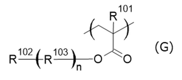

アリール基としては、例えば、フェニル基、ナフチル基、ビフェニル基、アントリル基などが挙げられる。
アルキル基は、直鎖状、分岐鎖状あるいは環状のいずれであってもよい。
「中断されていてもよい」、とは、アルキル基中の何れかの炭素―炭素原子間がヘテロ原子(すなわち酸素の場合はエーテル結合)で中断されていることを言う。
アルキレン基とは、アルキル基の水素原子を更に一つ取り除いて誘導される2価の基をいう。
本発明の保護膜形成用組成物は、上記式(A)で表される化合物や(B)溶剤の他に、(J)3員環構造もしくは4員環構造を持つ環状エーテルを含む、化合物(J)又は重合体(J)を含んでもよい。
ここで、3員環構造を持つ環状エーテルとしては例えば、エポキシ基が挙げられる。また、4員環構造を持つ環状エーテルとしては、例えば、オキセタニル基が挙げられる。
(J)化合物又は重合体のより好ましい実施態様としては、下記第3の態様で示される化合物、あるいは第4の態様で示される重合体などが挙げられる。
本発明で使用される(J)化合物として、例えば、以下の化合物が挙げられる。
係る化合物(以下、第3の態様における化合物ともいう)は、繰り返し構造単位を有しない化合物であって、
末端基(J1)、多価基(J2)、及び連結基(J3)を含み、
末端基(J1)は連結基(J3)のみと結合し、
多価基(J2)は連結基(J3)のみと結合し、
連結基(J3)は一方で末端基(J1)と、他方で多価基(J2)と結合し、任意選択的に別の連結基(J3)と結合してもよく、
末端基(J1)は下記式(I)の構造のいずれかであり、

Xはエーテル結合、エステル結合又は窒素原子を表し、Xがエーテル結合又はエステル結合のときn=1であり、Xが窒素原子のときn=2である。)
多価基(J2)は、
-O-、
脂肪族炭化水素基、
炭素原子数10未満の芳香族炭化水素基と脂肪族炭化水素基との組合せ、及び
炭素原子数10以上の芳香族炭化水素基と-O-との組合せ
からなる群より選択される2~4価の基であり、
連結基(J3)は芳香族炭化水素基を表す、
化合物である。
非限定的な例として、2価の脂肪族炭化水素基を例示すると、メチレン基、エチレン基、n-プロピレン基、イソプロピレン基、シクロプロピレン基、n-ブチレン基、イソブチレン基、s-ブチレン基、t-ブチレン基、シクロブチレン基、1-メチル-シクロプロピレン基、2-メチル-シクロプロピレン基、n-ペンチレン基、1-メチル-n-ブチレン基、2-メチル-n-ブチレン基、3-メチル-n-ブチレン基、1,1-ジメチル-n-プロピレン基、1,2-ジメチル-n-プロピレン基、2,2-ジメチル-n-プロピレン、1-エチル-n-プロピレン基、シクロペンチレン基、1-メチル-シクロブチレン基、2-メチル-シクロブチレン基、3-メチル-シクロブチレン基、1,2-ジメチル-シクロプロピレン基、2,3-ジメチル-シクロプロピレン基、1-エチル-シクロプロピレン基、2-エチル-シクロプロピレン基、n-ヘキシレン基、1-メチル-n-ペンチレン基、2-メチル-n-ペンチレン基、3-メチル-n-ペンチレン基、4-メチル-n-ペンチレン基、1,1-ジメチル-n-ブチレン基、1,2-ジメチル-n-ブチレン基、1,3-ジメチル-n-ブチレン基、2,2-ジメチル-n-ブチレン基、2,3-ジメチル-n-ブチレン基、3,3-ジメチル-n-ブチレン基、1-エチル-n-ブチレン基、2-エチル-n-ブチレン基、1,1,2-トリメチル-n-プロピレン基、1,2,2-トリメチル-n-プロピレン基、1-エチル-1-メチル-n-プロピレン基、1-エチル-2-メチル-n-プロピレン基、シクロヘキシレン基、1-メチル-シクロペンチレン基、2-メチル-シクロペンチレン基、3-メチル-シクロペンチレン基、1-エチル-シクロブチレン基、2-エチル-シクロブチレン基、3-エチル-シクロブチレン基、1,2-ジメチル-シクロブチレン基、1,3-ジメチル-シクロブチレン基、2,2-ジメチル-シクロブチレン基、2,3-ジメチル-シクロブチレン基、2,4-ジメチル-シクロブチレン基、3,3-ジメチル-シクロブチレン基、1-n-プロピル-シクロプロピレン基、2-n-プロピル-シクロプロピレン基、1-イソプロピル-シクロプロピレン基、2-イソプロピル-シクロプロピレン基、1,2,2-トリメチル-シクロプロピレン基、1,2,3-トリメチル-シクロプロピレン基、2,2,3-トリメチル-シクロプロピレン基、1-エチル-2-メチル-シクロプロピレン基、2-エチル-1-メチル-シクロプロピレン基、2-エチル-2-メチル-シクロプロピレン基、2-エチル-3-メチル-シクロプロピレン基、n-ヘプチレン基、n-オクチレン基、n-ノニレン基又はn-デカニレン基のアルキレン基が挙げられる。

Z1、Z2はそれぞれ独立に

Xはエーテル結合、エステル結合又は窒素原子を表し、Xがエーテル結合又はエステル結合のときn=1であり、Xが窒素原子のときn=2である。)
を表し、
Y1、Y2はそれぞれ独立に芳香族炭化水素基を表し、
X1、X2はそれぞれ独立に-Y1-Z1又は-Y2-Z2を表し、
n1、n2はそれぞれ独立に0~4の整数を表し、但しいずれかは1以上であり、
(X1)m1で規定するm1は0又は1を表し、
(X2)m2で規定するm2は0又は1を表し、
Qは-O-、脂肪族炭化水素基、炭素原子数10未満の芳香族炭化水素基と脂肪族炭化水素基との組合せ、及び炭素原子数10以上の芳香族炭化水素基と-O-との組合せからなる群より選択される(n1+n2)価の基を表す。)
Qは、2~4価の基であることが好ましい。

本発明で使用される(J)重合体として、例えば、以下の重合体が挙げられる。
係る重合体(以下、第4の態様における重合体ともいう)は、下記式(1-1)で表される単位構造を有する重合体である:
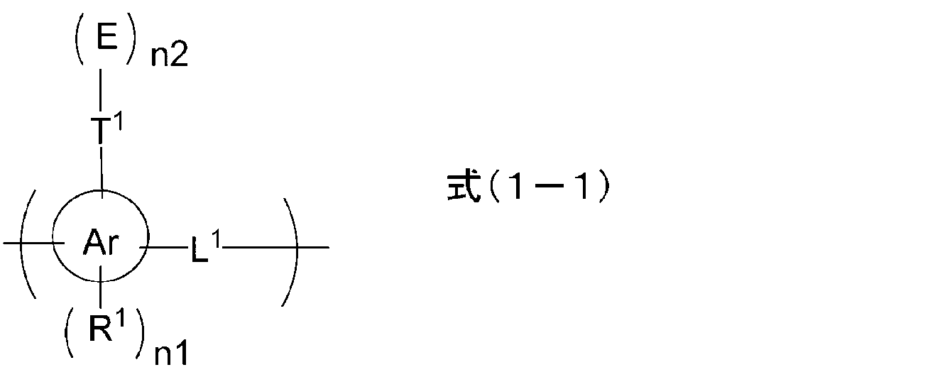

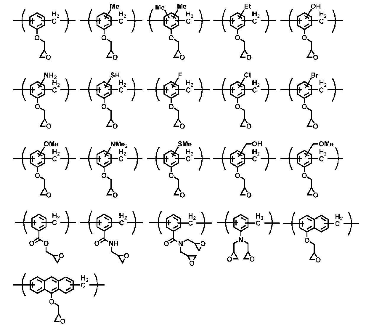
本発明のレジスト下層膜形成用組成物は、
(A)上記式(A)で表される化合物、及び
(B)溶剤、を含む。
上述した本発明の保護膜形成用組成物は、半導体用ウエットエッチング液に対し優れた耐性を示すだけでなく、レジスト下層膜形成用の組成物としても有効に使用することができる。
本発明のレジスト下層膜形成用組成物に係る用語の説明は、上記保護膜形成用組成物での説明内容と同一である。
以下、本発明に係る保護膜形成用組成物(レジスト下層膜形成用組成物)を用いたレジストパターン付き基板の製造方法及び半導体装置の製造方法について説明する。
露光は、所定のパターンを形成するためのマスク(レチクル)を通して行われ、例えば、i線、KrFエキシマレーザー、ArFエキシマレーザー、EUV(極端紫外線)またはEB(電子線)が使用される。現像にはアルカリ現像液が用いられ、現像温度5℃~50℃、現像時間10秒~300秒から適宜選択される。アルカリ現像液としては、例えば、水酸化ナトリウム、水酸化カリウム、炭酸ナトリウム、ケイ酸ナトリウム、メタケイ酸ナトリウム、アンモニア水等の無機アルカリ類、エチルアミン、n-プロピルアミン等の第一アミン類、ジエチルアミン、ジ-n-ブチルアミン等の第二アミン類、トリエチルアミン、メチルジエチルアミン等の第三アミン類、ジメチルエタノールアミン、トリエタノールアミン等のアルコールアミン類、テトラメチルアンモニウムヒドロキシド、テトラエチルアンモニウムヒドロキシド、コリン等の第4級アンモニウム塩、ピロール、ピペリジン等の環状アミン類、等のアルカリ類の水溶液を使用することができる。さらに、上記アルカリ類の水溶液にイソプロピルアルコール等のアルコール類、ノニオン系等の界面活性剤を適当量添加して使用することもできる。これらの中で好ましい現像液は第四級アンモニウム塩、さらに好ましくはテトラメチルアンモニウムヒドロキシド及びコリンである。さらに、これらの現像液に界面活性剤などを加えることもできる。アルカリ現像液に代えて、酢酸ブチル等の有機溶媒で現像を行い、フォトレジストのアルカリ溶解速度が向上していない部分を現像する方法を用いることもできる。
カラム温度:40℃
溶媒:テトラヒドロフラン(THF)
流量:0.35mL/分
標準試料:ポリスチレン(東ソー(株)製)
トリアジントリオン型エポキシ樹脂(製品名:TEPIC、日産化学株式会社製)5.00g、3,4-ジヒドロキシヒドロ柱皮酸9.31g、テトラブチルホスホニウムブロマイド0.43g、プロピレングリコールモノメチルエーテル58.95gを反応フラスコに加え、窒素雰囲気下、内温105℃で24時間加熱撹拌した。
得られた反応生成物は下記式(I-1)に相当し、GPCによるポリスチレン換算で測定される重量平均分子量Mwは768であった。
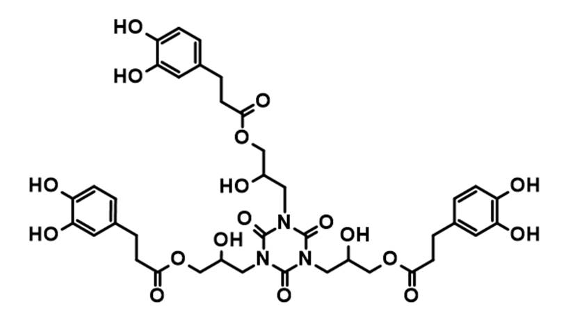
トリアジントリオン型エポキシ樹脂(製品名:TEPIC、日産化学株式会社製)3.00g、シアノ酢酸2.61g、テトラブチルホスホニウムブロマイド0.26g、プロピレングリコールモノメチルエーテル23.46gを反応フラスコに加え、窒素雰囲気下、内温80℃で24時間加熱撹拌した。続いて、酢酸アンモニウム0.12g、3,4-ジヒドロキシベンズアルデヒド4.24gをプロピレングリコールモノメチルエーテル17.42gで溶解させた溶液を系内に加え、さらに内温80℃で24時間加熱撹拌した。
得られた反応生成物は下記式(I-2)に相当し、GPCによるポリスチレン換算で測定される重量平均分子量Mwは773であった。
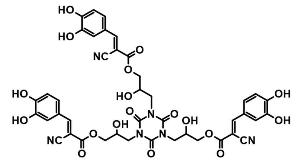
トリアジントリオン型エポキシ樹脂(製品名:TEPIC、日産化学株式会社製)3.00g、シアノ酢酸2.61g、テトラブチルホスホニウムブロマイド0.26g、プロピレングリコールモノメチルエーテル23.46gを反応フラスコに加え、窒素雰囲気下、内温80℃で24時間加熱撹拌した。続いて、4-ヒドロキシベンズアルデヒド3.67gをプロピレングリコールモノメチルエーテル14.68gで溶解させた溶液を系内に加え、さらに内温80℃で24時間加熱撹拌した。
得られた反応生成物は下記式(I-3)に相当し、GPCによるポリスチレン換算で測定される重量平均分子量Mwは655であった。
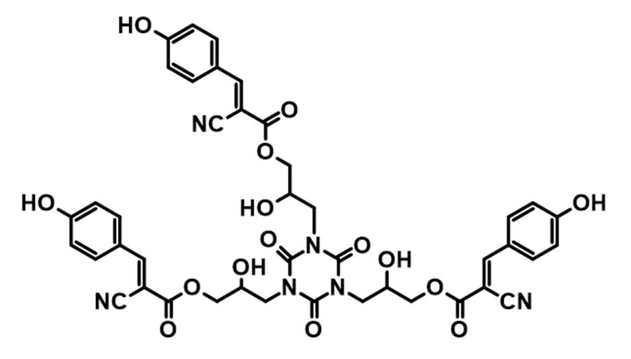
上記式(I-1)に相当する反応生成物の溶液(固形分16.7質量%)2.875gに、架橋剤としてテトラメトキシメチルグリコールウリル(商品名:POWDER LINK[登録商標]1174、日本サイエンティックインダストリーズ(株)製)0.096g、架橋触媒としてピリジニウム-トリフルオロメタンスルホナート0.024g、界面活性剤としてメガファックR-30N(DIC(株)製、商品名)0.001g、プロピレングリコールモノメチルエーテル7.00gを加え、保護膜形成用組成物の溶液を調製した。
上記式(I-1)に相当する反応生成物の溶液(固形分16.7質量%)2.875gに、架橋剤としてテトラメトキシメチルグリコールウリル(商品名:POWDER LINK[登録商標]1174、日本サイエンティックインダストリーズ(株)製)0.096g、架橋触媒としてピリジニウム-p-トルエンスルホナート0.024g、界面活性剤としてメガファックR-30N(DIC(株)製、商品名)0.001g、プロピレングリコールモノメチルエーテル7.00gを加え、保護膜形成用組成物の溶液を調製した。
上記式(I-1)に相当する反応生成物の溶液(固形分16.7質量%)2.875gに、架橋剤としてテトラメトキシメチルグリコールウリル(商品名:POWDER LINK[登録商標]1174、日本サイエンティックインダストリーズ(株)製)0.096g、架橋触媒としてピリジニウム-p-フェノールスルホナート0.024g、界面活性剤としてメガファックR-30N(DIC(株)製、商品名)0.001g、プロピレングリコールモノメチルエーテル7.00gを加え、保護膜形成用組成物の溶液を調製した。
上記式(I-1)に相当する反応生成物の溶液(固形分16.7質量%)2.875gに、架橋剤として3,3’,5,5’-テトラキス(メトキシメチル)-4,4’-ジヒドロキシビフェニル(製品名:TMOM-BP、本州化学工業株式会社製)0.096g、架橋触媒としてピリジニウム-トリフルオロメタンスルホナート0.024g、界面活性剤としてメガファックR-30N(DIC(株)製、商品名)0.001g、プロピレングリコールモノメチルエーテル7.00gを加え、保護膜形成用組成物の溶液を調製した。
上記式(I-1)に相当する反応生成物の溶液(固形分16.7質量%)2.875gに、架橋剤として3,3’,5,5’-テトラキス(メトキシメチル)-4,4’-ジヒドロキシビフェニル(製品名:TMOM-BP、本州化学工業株式会社製)0.096g、架橋触媒としてピリジニウム-p-トルエンスルホナート0.024g、界面活性剤としてメガファックR-30N(DIC(株)製、商品名)0.001g、プロピレングリコールモノメチルエーテル7.00gを加え、保護膜形成用組成物の溶液を調製した。
上記式(I-1)に相当する反応生成物の溶液(固形分16.7質量%)2.875gに、架橋剤として3,3’,5,5’-テトラキス(メトキシメチル)-4,4’-ジヒドロキシビフェニル(製品名:TMOM-BP、本州化学工業株式会社製)0.096g、架橋触媒としてピリジニウム-p-フェノールスルホナート0.024g、界面活性剤としてメガファックR-30N(DIC(株)製、商品名)0.001g、プロピレングリコールモノメチルエーテル7.00gを加え、保護膜形成用組成物の溶液を調製した。
上記式(I-2)に相当する反応生成物の溶液(固形分17.3質量%)4.149gに、架橋剤として3,3’,5,5’-テトラキス(メトキシメチル)-4,4’-ジヒドロキシビフェニル(製品名:TMOM-BP、本州化学工業株式会社製)0.144g、架橋触媒としてピリジニウム-トリフルオロメタンスルホナート0.036g、界面活性剤としてメガファックR-30N(DIC(株)製、商品名)0.001g、プロピレングリコールモノメチルエーテル10.67gを加え、保護膜形成用組成物の溶液を調製した。
下記式(I-4)で示される薬液耐性保護膜形成組成物のアクリル樹脂の溶液(固形分20.0質量%)4.490gに、添加剤として上記式(I-1)に相当する反応生成物の溶液(固形分16.7質量%)1.073g、架橋剤としてテトラメトキシメチルグリコールウリル(商品名:POWDER LINK[登録商標]1174、日本サイエンティックインダストリーズ(株)製)0.179g、架橋触媒としてピリジニウム-トリフルオロメタンスルホナート0.045g、界面活性剤としてメガファックR-30N(DIC(株)製、商品名)0.001g、乳酸エチル9.50g、プロピレングリコールモノメチルエーテル4.71gを加え、保護膜形成用組成物の溶液を調製した。
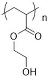
上記式(I-4)で示される薬液耐性保護膜形成組成物のアクリル樹脂の溶液(固形分20.0質量%)4.491gに、添加剤として上記式(I-2)に相当する反応生成物の溶液(固形分17.3質量%)1.033g、架橋剤としてテトラメトキシメチルグリコールウリル(商品名:POWDER LINK[登録商標]1174、日本サイエンティックインダストリーズ(株)製)0.179g、架橋触媒としてピリジニウム-トリフルオロメタンスルホナート0.045g、界面活性剤としてメガファックR-30N(DIC(株)製、商品名)0.001g、乳酸エチル9.50g、プロピレングリコールモノメチルエーテル4.76gを加え、保護膜形成用組成物の溶液を調製した。
下記式(I-5)で示される薬液耐性保護膜形成組成物のアクリル樹脂の溶液(固形分30.2質量%)3.909gに、添加剤として上記式(I-1)に相当する反応生成物の溶液(固形分16.7質量%)0.708g、界面活性剤としてメガファックR-30N(DIC(株)製、商品名)0.001g、プロピレングリコールモノメチルエーテル5.02g、プロピレングリコールモノメチルエーテルアセテート10.36gを加え、保護膜形成用組成物の溶液を調整した。
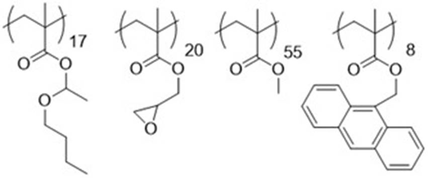
上記式(I-5)で示される薬液耐性保護膜形成組成物のアクリル樹脂の溶液(固形分30.2質量%)3.909gに、添加剤として上記式(I-2)に相当する反応生成物の溶液(固形分17.3質量%)0.681g、界面活性剤としてメガファックR-30N(DIC(株)製、商品名)0.001g、プロピレングリコールモノメチルエーテル5.05g、プロピレングリコールモノメチルエーテルアセテート10.36gを加え、保護膜形成用組成物の溶液を調製した。
上記式(I-3)に相当する反応生成物の溶液(固形分13.9質量%)5.187gに、架橋剤として3,3’,5,5’-テトラキス(メトキシメチル)-4,4’-ジヒドロキシビフェニル(製品名:TMOM-BP、本州化学工業株式会社製)0.144g、架橋触媒としてピリジニウム-トリフルオロメタンスルホナート0.036g、界面活性剤としてメガファックR-30N(DIC(株)製、商品名)0.001g、プロピレングリコールモノメチルエーテル10.67gを加え、保護膜形成用組成物の溶液を調製した。
上記式(I-4)で示される保護膜形成用組成物のアクリル樹脂の溶液(固形分20.0質量%)5.209gに、架橋剤としてテトラメトキシメチルグリコールウリル(商品名:POWDER LINK[登録商標]1174、日本サイエンティックインダストリーズ(株)製)0.208g、架橋触媒としてピリジニウム-トリフルオロメタンスルホナート0.052g、界面活性剤としてメガファックR-30N(DIC(株)製、商品名)0.001g、乳酸エチル8.92g、プロピレングリコールモノメチルエーテル5.61gを加え、保護膜形成用組成物の溶液を調製した。
上記式(I-5)で示される保護膜形成用組成物のアクリル樹脂の溶液(固形分30.2質量%)4.299gに、界面活性剤としてメガファックR-30N(DIC(株)製、商品名)0.001g、プロピレングリコールモノメチルエーテル5.61g、プロピレングリコールモノメチルエーテルアセテート10.09gを加え、保護膜形成用組成物の溶液を調製した。
実施例1~実施例11及び比較例1~比較例3で調製された保護膜形成用組成物のそれぞれをスピンコーターにてシリコンウェハー上に塗布(スピンコート)した。
塗布後のシリコンウェハーをホットプレート上で220℃、1分間加熱し、膜厚150nmの被膜(保護膜)を形成した。次に、保護膜のレジスト溶剤耐性を確認するため、保護膜形成後のシリコンウェハーを、プロピレングリコールモノメチルエーテルとプロピレングリコールモノメチルエーテルアセテートとを質量比7対3で混合した溶剤に1分間浸漬し、スピンドライ後に100℃、30秒間ベークした。混合溶剤を浸漬する前後の保護膜の膜厚を光干渉膜厚計(製品名:ナノスペック6100、ナノメトリクス・ジャパン株式会社製)で測定した。
レジスト溶剤耐性の評価は、((溶剤浸漬前の膜厚)-(溶剤浸漬後の膜厚))÷(溶剤浸漬前の膜厚)×100の計算式から、溶剤浸漬によって除去された保護膜の膜厚減少率(%)を算出、評価した。結果を下記表1に示す。なお、膜厚減少率が約1%以下であれば十分なレジスト溶剤耐性を有すると言える。

塩基性過酸化水素水への耐性評価として、実施例1~実施例6、実施例8~実施例11及び比較例2~比較例3で調製された保護膜形成組成物のそれぞれを50nm膜厚の窒化チタン(TiN)蒸着基板に塗布し、220℃、1分間加熱することで、膜厚150nmとなるように保護膜を成膜した。次に、28%アンモニア水、33%過酸化水素、水をそれぞれ質量比1対4対20となるように混合し、塩基性過酸化水素水を調製した。上記の保護膜形成用組成物を塗布したTiN蒸着基板を、50℃に加温したこの塩基性過酸化水素水中に浸漬し、浸漬直後から保護膜が基板から剥離するまでの時間(剥離時間)を測定した。塩基性過酸化水素水への耐性試験の結果を下記表2に示す。尚、剥離時間が長くなるほど、塩基性過酸化水素水を用いたウエットエッチング液への耐性が高いと言える。
酸性過酸化水素水への耐性評価として、実施例1~実施例11及び比較例1で調製された保護膜形成組成物のそれぞれを50nm膜厚のTiN蒸着基板に塗布し、220℃、1分間加熱することで、膜厚150nmとなるように保護膜を成膜した。次に、前記の保護膜形成組成物を塗布したTiN蒸着基板を70℃に加温したこの20質量%過酸化水素水中に浸漬し、浸漬直後から保護膜にダメージが入るまでの時間を測定した。過酸化水素水への耐性試験の結果を表2に示す。尚、ダメージが入るまでの時間が長くなるほど、過酸化水素水を用いたウエットエッチング液への耐性が高いと言える。

また、実施例1~実施例6の結果より、架橋剤としてはフェノプラスト架橋剤、架橋触媒としては超強酸を発生するものを選択することで、塩基性過酸化水素水を用いたウエットエッチング液に対して良好な耐性を示すと言える。したがって、実施例1~実施例11は、比較例1~比較例3と比較して、塩基性過酸化水素水もしくは過酸化水素水もしくはその両方に対して、良好な薬液耐性を示すことから、半導体用ウエットエッチング液に対する保護膜として有用である。
Claims (14)
- (A)下記式(A)で表される化合物、及び
(B)溶剤、
を含む、半導体用ウエットエッチング液に対する保護膜形成用組成物。

- 前記式(A)中、前記Xが炭素原子数2~50の2価の有機基である場合、前記Xは、下記式(A-1)で表される2価の有機基であり、前記Xが炭素原子数2~50の2価以外のn価の有機基である場合、前記Xは、下記式(A-2)で表されるn価の有機基である、請求項1に記載の保護膜形成用組成物。


式(A-2)中、Z2は、置換基を有してもよい芳香族環、置換基を有してもよい脂肪族環、及び置換基を有してもよい複素環からなる群から選択される環を含むn価の有機基、又は前記環と炭素原子数1~6のアルキレン基とを含むn価の有機基を表し、mは0または1を表し、Lは、-O-、または-C(=O)-O-を表す。) - 前記保護膜形成用組成物が、更に、(C)架橋剤、(D)架橋触媒、(E)界面活性剤のうち少なくともいずれかを含有する、請求項1に記載の保護膜形成用組成物。
- 前記保護膜形成用組成物が、更に、(F)(メタ)アクリロイル基、スチレン基、フェノール性ヒドロキシ基、エーテル基、エポキシ基、もしくはオキセタニル基を含む化合物、または重合体を含有する、請求項1に記載の保護膜形成用組成物。
- 前記保護膜形成用組成物が、更に、(G)下記式(G)で示される繰り返し構造単位を有する重合体を含有する、請求項4に記載の保護膜形成用組成物。
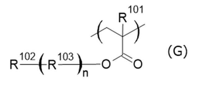

- 前記保護膜形成用組成物が、更に、(J)3員環構造もしくは4員環構造を持つ環状エーテルを含む、化合物(J)又は重合体(J)を含有する、請求項4に記載の保護膜形成用組成物。
- 請求項1~6のいずれかに記載の保護膜形成用組成物からなる塗布膜の焼成物であることを特徴とする半導体用ウエットエッチング液に対する保護膜。
- (A)下記式(A)で表される化合物、及び
(B)溶剤、
を含む、レジスト下層膜形成用組成物。
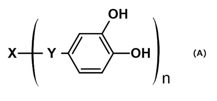
- 前記式(A)中、前記Xが炭素原子数2~50の2価の有機基である場合、前記Xは、下記式(A-1)で表される2価の有機基であり、前記Xが炭素原子数2~50の2価以外のn価の有機基である場合、前記Xは、下記式(A-2)で表されるn価の有機基である、請求項8に記載のレジスト下層膜形成用組成物。
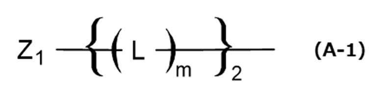

式(A-2)中、Z2は、置換基を有してもよい芳香族環、置換基を有してもよい脂肪族環、及び置換基を有してもよい複素環からなる群から選択される環を含むn価の有機基、又は前記環と炭素原子数1~6のアルキレン基とを含むn価の有機基を表し、mは0または1を表し、Lは、-O-、または-C(=O)-O-を表す。) - 請求項8に記載のレジスト下層膜形成用組成物からなる塗布膜の焼成物であることを特徴とするレジスト下層膜。
- 請求項1~6のいずれかに記載の保護膜形成用組成物を、段差を有する半導体基板上に塗布し焼成して保護膜を形成する工程を含む、半導体の製造に用いることを特徴とする保護膜付き基板の製造方法。
- 請求項1~6のいずれかに記載の保護膜形成用組成物、又は請求項8または9に記載のレジスト下層膜形成用組成物を半導体基板上に塗布し焼成してレジスト下層膜としての保護膜を形成する工程、該保護膜上にレジスト膜を形成し、次いで露光、現像してレジストパターンを形成する工程を含み、半導体の製造に用いることを特徴とするレジストパターン付き基板の製造方法。
- 表面に無機膜が形成されていてもよい半導体基板上に、請求項1~6のいずれかに記載の保護膜形成用組成物を用いて保護膜を形成し、前記保護膜上にレジストパターンを形成し、前記レジストパターンをマスクとして前記保護膜をドライエッチングし、前記無機膜又は前記半導体基板の表面を露出させ、ドライエッチング後の前記保護膜をマスクとして、半導体用ウエットエッチング液を用いて前記無機膜又は前記半導体基板をウエットエッチング及び洗浄する工程を含む半導体装置の製造方法。
- 表面に無機膜が形成されていてもよい半導体基板上に、請求項8または9に記載のレジスト下層膜形成用組成物を用いてレジスト下層膜を形成し、前記レジスト下層膜上にレジストパターンを形成し、前記レジストパターンをマスクとして前記レジスト下層膜をドライエッチングし、前記無機膜又は前記半導体基板の表面を露出させ、ドライエッチング後の前記レジスト下層膜をマスクとして、前記無機膜又は前記半導体基板をエッチングする工程を含む半導体装置の製造方法。
Priority Applications (4)
| Application Number | Priority Date | Filing Date | Title |
|---|---|---|---|
| US18/714,440 US20250034427A1 (en) | 2021-11-29 | 2022-10-07 | Chemical-resistant protective film-forming composition having catechol group |
| CN202280078453.9A CN118318208A (zh) | 2021-11-29 | 2022-10-07 | 具有儿茶酚基的药液耐性保护膜形成用组合物 |
| KR1020247018852A KR20240112860A (ko) | 2021-11-29 | 2022-10-07 | 카테콜기를 갖는 약액 내성 보호막 형성용 조성물 |
| JP2023563541A JPWO2023095461A1 (ja) | 2021-11-29 | 2022-10-07 |
Applications Claiming Priority (2)
| Application Number | Priority Date | Filing Date | Title |
|---|---|---|---|
| JP2021-193025 | 2021-11-29 | ||
| JP2021193025 | 2021-11-29 |
Publications (1)
| Publication Number | Publication Date |
|---|---|
| WO2023095461A1 true WO2023095461A1 (ja) | 2023-06-01 |
Family
ID=86539241
Family Applications (1)
| Application Number | Title | Priority Date | Filing Date |
|---|---|---|---|
| PCT/JP2022/037533 Ceased WO2023095461A1 (ja) | 2021-11-29 | 2022-10-07 | カテコール基を有する薬液耐性保護膜形成用組成物 |
Country Status (6)
| Country | Link |
|---|---|
| US (1) | US20250034427A1 (ja) |
| JP (1) | JPWO2023095461A1 (ja) |
| KR (1) | KR20240112860A (ja) |
| CN (1) | CN118318208A (ja) |
| TW (1) | TW202328260A (ja) |
| WO (1) | WO2023095461A1 (ja) |
Cited By (1)
| Publication number | Priority date | Publication date | Assignee | Title |
|---|---|---|---|---|
| WO2026023597A1 (ja) * | 2024-07-23 | 2026-01-29 | 日産化学株式会社 | 保護膜形成用組成物、保護膜、基板の製造方法及び半導体装置の製造方法 |
Citations (4)
| Publication number | Priority date | Publication date | Assignee | Title |
|---|---|---|---|---|
| WO2018052130A1 (ja) * | 2016-09-16 | 2018-03-22 | 日産化学工業株式会社 | 保護膜形成組成物 |
| JP2018173521A (ja) * | 2017-03-31 | 2018-11-08 | 信越化学工業株式会社 | レジスト下層膜材料、パターン形成方法、及びレジスト下層膜形成方法 |
| JP2022083466A (ja) * | 2020-11-25 | 2022-06-06 | 信越化学工業株式会社 | レジスト下層膜材料、パターン形成方法、及びレジスト下層膜形成方法 |
| WO2022186231A1 (ja) * | 2021-03-03 | 2022-09-09 | 日産化学株式会社 | ベンジリデンシアノ酢酸エステル基を有するレジスト下層膜形成組成物 |
Family Cites Families (1)
| Publication number | Priority date | Publication date | Assignee | Title |
|---|---|---|---|---|
| JP6718406B2 (ja) | 2017-03-31 | 2020-07-08 | 信越化学工業株式会社 | レジスト下層膜材料、パターン形成方法、及びレジスト下層膜形成方法 |
-
2022
- 2022-10-07 CN CN202280078453.9A patent/CN118318208A/zh active Pending
- 2022-10-07 JP JP2023563541A patent/JPWO2023095461A1/ja active Pending
- 2022-10-07 WO PCT/JP2022/037533 patent/WO2023095461A1/ja not_active Ceased
- 2022-10-07 KR KR1020247018852A patent/KR20240112860A/ko active Pending
- 2022-10-07 US US18/714,440 patent/US20250034427A1/en active Pending
- 2022-10-18 TW TW111139378A patent/TW202328260A/zh unknown
Patent Citations (4)
| Publication number | Priority date | Publication date | Assignee | Title |
|---|---|---|---|---|
| WO2018052130A1 (ja) * | 2016-09-16 | 2018-03-22 | 日産化学工業株式会社 | 保護膜形成組成物 |
| JP2018173521A (ja) * | 2017-03-31 | 2018-11-08 | 信越化学工業株式会社 | レジスト下層膜材料、パターン形成方法、及びレジスト下層膜形成方法 |
| JP2022083466A (ja) * | 2020-11-25 | 2022-06-06 | 信越化学工業株式会社 | レジスト下層膜材料、パターン形成方法、及びレジスト下層膜形成方法 |
| WO2022186231A1 (ja) * | 2021-03-03 | 2022-09-09 | 日産化学株式会社 | ベンジリデンシアノ酢酸エステル基を有するレジスト下層膜形成組成物 |
Cited By (1)
| Publication number | Priority date | Publication date | Assignee | Title |
|---|---|---|---|---|
| WO2026023597A1 (ja) * | 2024-07-23 | 2026-01-29 | 日産化学株式会社 | 保護膜形成用組成物、保護膜、基板の製造方法及び半導体装置の製造方法 |
Also Published As
| Publication number | Publication date |
|---|---|
| KR20240112860A (ko) | 2024-07-19 |
| TW202328260A (zh) | 2023-07-16 |
| JPWO2023095461A1 (ja) | 2023-06-01 |
| US20250034427A1 (en) | 2025-01-30 |
| CN118318208A (zh) | 2024-07-09 |
Similar Documents
| Publication | Publication Date | Title |
|---|---|---|
| JP6652747B2 (ja) | アリーレン基を有するポリマーを含むレジスト下層膜形成組成物 | |
| JP7396049B2 (ja) | ジスルフィド構造を有するレジスト下層膜形成組成物 | |
| JP7302480B2 (ja) | ジオール構造を有する保護膜形成組成物 | |
| JP2023157924A (ja) | アセタール構造を有する保護膜形成組成物 | |
| TWI830801B (zh) | 包含與具有縮水甘油基的伸芳基化合物之聚合生成物之耐化學性保護膜形成組成物 | |
| JP7666327B2 (ja) | レジスト下層膜形成組成物 | |
| JP2023184588A (ja) | ジオール構造を末端に有する重合生成物を含む薬液耐性保護膜形成組成物 | |
| CN116057103B (zh) | 药液耐性保护膜 | |
| WO2022186231A1 (ja) | ベンジリデンシアノ酢酸エステル基を有するレジスト下層膜形成組成物 | |
| KR20240112860A (ko) | 카테콜기를 갖는 약액 내성 보호막 형성용 조성물 | |
| KR102800934B1 (ko) | 약액 내성 보호막 | |
| TWI846857B (zh) | 包含羥芳基末端之聚合物之耐藥液性保護膜形成組成物 | |
| WO2023100506A1 (ja) | ヒドロキシケイ皮酸誘導体を有するレジスト下層膜形成用組成物 | |
| JP7275676B2 (ja) | レジスト下層膜形成組成物 | |
| TWI921328B (zh) | 半導體裝置的製造方法 | |
| JP7859567B2 (ja) | 薬液耐性保護膜 | |
| TW202613243A (zh) | 半導體裝置的製造方法 | |
| KR20250107863A (ko) | 쿠르쿠민 유도체를 갖는 레지스트 하층막 형성용 조성물 | |
| WO2023084961A1 (ja) | 薬液耐性保護膜 | |
| WO2020184642A1 (ja) | レジスト下層膜形成組成物 |
Legal Events
| Date | Code | Title | Description |
|---|---|---|---|
| 121 | Ep: the epo has been informed by wipo that ep was designated in this application |
Ref document number: 22898245 Country of ref document: EP Kind code of ref document: A1 |
|
| ENP | Entry into the national phase |
Ref document number: 2023563541 Country of ref document: JP Kind code of ref document: A |
|
| WWE | Wipo information: entry into national phase |
Ref document number: 202280078453.9 Country of ref document: CN |
|
| WWE | Wipo information: entry into national phase |
Ref document number: 18714440 Country of ref document: US |
|
| ENP | Entry into the national phase |
Ref document number: 20247018852 Country of ref document: KR Kind code of ref document: A |
|
| NENP | Non-entry into the national phase |
Ref country code: DE |
|
| 122 | Ep: pct application non-entry in european phase |
Ref document number: 22898245 Country of ref document: EP Kind code of ref document: A1 |