WO2023095443A1 - 半導体パッケージ、および、モジュール - Google Patents
半導体パッケージ、および、モジュール Download PDFInfo
- Publication number
- WO2023095443A1 WO2023095443A1 PCT/JP2022/036689 JP2022036689W WO2023095443A1 WO 2023095443 A1 WO2023095443 A1 WO 2023095443A1 JP 2022036689 W JP2022036689 W JP 2022036689W WO 2023095443 A1 WO2023095443 A1 WO 2023095443A1
- Authority
- WO
- WIPO (PCT)
- Prior art keywords
- semiconductor package
- chip
- substrate
- measurement unit
- information
- Prior art date
- Legal status (The legal status is an assumption and is not a legal conclusion. Google has not performed a legal analysis and makes no representation as to the accuracy of the status listed.)
- Ceased
Links
Images






Classifications
-
- G—PHYSICS
- G01—MEASURING; TESTING
- G01P—MEASURING LINEAR OR ANGULAR SPEED, ACCELERATION, DECELERATION, OR SHOCK; INDICATING PRESENCE, ABSENCE, OR DIRECTION, OF MOVEMENT
- G01P1/00—Details of instruments
-
- G—PHYSICS
- G01—MEASURING; TESTING
- G01B—MEASURING LENGTH, THICKNESS OR SIMILAR LINEAR DIMENSIONS; MEASURING ANGLES; MEASURING AREAS; MEASURING IRREGULARITIES OF SURFACES OR CONTOURS
- G01B21/00—Measuring arrangements or details thereof, where the measuring technique is not covered by the other groups of this subclass, unspecified or not relevant
- G01B21/30—Measuring arrangements or details thereof, where the measuring technique is not covered by the other groups of this subclass, unspecified or not relevant for measuring roughness or irregularity of surfaces
-
- G—PHYSICS
- G01—MEASURING; TESTING
- G01P—MEASURING LINEAR OR ANGULAR SPEED, ACCELERATION, DECELERATION, OR SHOCK; INDICATING PRESENCE, ABSENCE, OR DIRECTION, OF MOVEMENT
- G01P15/00—Measuring acceleration; Measuring deceleration; Measuring shock, i.e. sudden change of acceleration
- G01P15/02—Measuring acceleration; Measuring deceleration; Measuring shock, i.e. sudden change of acceleration by making use of inertia forces using solid seismic masses
-
- H—ELECTRICITY
- H10—SEMICONDUCTOR DEVICES; ELECTRIC SOLID-STATE DEVICES NOT OTHERWISE PROVIDED FOR
- H10W—GENERIC PACKAGES, INTERCONNECTIONS, CONNECTORS OR OTHER CONSTRUCTIONAL DETAILS OF DEVICES COVERED BY CLASS H10
- H10W42/00—Arrangements for protection of devices
-
- H—ELECTRICITY
- H10—SEMICONDUCTOR DEVICES; ELECTRIC SOLID-STATE DEVICES NOT OTHERWISE PROVIDED FOR
- H10W—GENERIC PACKAGES, INTERCONNECTIONS, CONNECTORS OR OTHER CONSTRUCTIONAL DETAILS OF DEVICES COVERED BY CLASS H10
- H10W70/00—Package substrates; Interposers; Redistribution layers [RDL]
- H10W70/60—Insulating or insulated package substrates; Interposers; Redistribution layers
-
- H—ELECTRICITY
- H10—SEMICONDUCTOR DEVICES; ELECTRIC SOLID-STATE DEVICES NOT OTHERWISE PROVIDED FOR
- H10W—GENERIC PACKAGES, INTERCONNECTIONS, CONNECTORS OR OTHER CONSTRUCTIONAL DETAILS OF DEVICES COVERED BY CLASS H10
- H10W90/00—Package configurations
Definitions
- This technology relates to semiconductor packages. More specifically, it relates to a semiconductor package and a module in which a plurality of chips are stacked and mounted.
- a semiconductor package has been proposed in which a first substrate, a circuit board, and an opening substrate provided with an opening are laminated, and a subchip is mounted in a space formed by the opening and the circuit board (for example, See Patent Document 1.).
- the subchip is provided with a gyro sensor and the like.
- the use of an opening substrate facilitates the mounting of subchips.
- the first substrate and the circuit substrate may generate heat during circuit operation, and warp may occur in these substrates.
- a sensor such as a gyro sensor is provided in the sub-chip, there is a risk that the measurement accuracy of the sensor may deteriorate due to warping of the substrate.
- This technology was created in view of this situation, and aims to improve the measurement accuracy of sensors in semiconductor packages equipped with sensors.
- the present technology has been made to solve the above-described problems, and a first aspect thereof includes a laminated chip that measures temperature and estimates the degree of warpage of itself from the temperature, and a predetermined physical quantity.
- the semiconductor package includes a measurement unit that performs a process of measuring to generate measurement information and a process of correcting the measurement information based on the degree of warpage. This brings about the effect of improving the measurement accuracy of the sensor in the measurement unit.
- the measurement unit may correct the measurement information based on the temperature and the degree of warpage. This brings about the effect of further improving the measurement accuracy.
- the first side surface further includes a substrate having a cavity formed in a predetermined substrate plane, the chip plane of the laminated chip is connected to a predetermined region around the cavity in the substrate plane, and the A measurement unit may be arranged in a region of the chip plane exposed in the cavity.
- a ground pattern and a terminal arranged in the vicinity of the ground pattern may be arranged in a predetermined area around the cavity on the substrate plane. This brings about an effect that the laminated chip and the substrate are electrically connected.
- a ground pattern including an island-shaped region and terminals formed in the island-shaped region may be arranged in a predetermined region around the cavity on the substrate plane. good. This brings about the effect of reducing the resistance value of the ground pattern.
- the first side surface may further include dummy silicon arranged in a region exposed in the cavity on the chip plane. This brings about the effect of suppressing the warp of the laminated chip and the concentration of heat distribution.
- the laminated chip may include a plurality of laminated chips, and any one of the plurality of chips and the substrate may be connected by a wire. This brings about an effect that the laminated chip and the substrate are electrically connected.
- the laminated chip and the substrate may be connected by resin. This provides an effect of facilitating connection between the laminated chip and the substrate.
- the first side surface may further include a metal plate attached to the substrate. This brings about the effect of suppressing warpage of the substrate.
- the measurement unit includes an inertia sensor having a movable portion exposed in the cavity and generating inertia information as the measurement information, and correcting the inertia information based on the degree of warpage.
- a correction circuit may be provided. This brings about the effect of improving the measurement accuracy of the inertial sensor.
- the measurement unit may further include a silicon cap that seals the movable portion.
- the laminated chip may include a sensor chip that generates image data. This brings about the effect that the image data is imaged.
- the sensor chip may process the image data using the corrected measurement information. This brings about the effect of improving the image quality of the image data.
- a second aspect of the present technology includes a layered chip that measures temperature and estimates the degree of warpage of itself from the temperature, a process of measuring a predetermined physical quantity to generate measurement information, and the degree of warpage. and a measurement unit for correcting the measurement information based on the measurement information. This brings about the effect of improving the measurement accuracy of the sensor in the measurement unit provided in the module.
- FIG. 1 is a block diagram showing a configuration example of a semiconductor package according to a first embodiment of the present technology
- FIG. 1 is an example of a cross-sectional view of a semiconductor package provided with a plurality of inertial measurement units according to a first embodiment of the present technology
- FIG. It is an example of the sectional view of the semiconductor package which reduced MEMS in a 1st embodiment of this art.
- FIG. 1 is a block diagram showing a schematic configuration example of a vehicle control system;
- FIG. 4 is an explanatory diagram showing an example of an installation position of an imaging unit;
- First Embodiment Example of Drift Correction of Inertial Information
- Second embodiment an example of sealing the movable part with a silicon cap and correcting the drift of the inertia information
- Third Embodiment Example in which Dummy Silicon is Placed and Inertial Information is Drift Corrected
- Fourth Embodiment Example of wire bonding and drift correction of inertia information
- Fifth Embodiment Example of Adhering a Metal Plate to a Substrate and Correcting Drift of Inertial Information
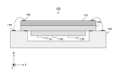
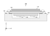
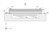
- FIG. 1 is a cross-sectional view showing one configuration example of a semiconductor package 100 according to a first embodiment of the present technology.
- This semiconductor package 100 is a package to be mounted on an imaging device or the like, and includes a layered chip 125 , an inertial measurement unit (IMU: Inertial Measurement Unit) 130 and a substrate 150 .
- Stacked chip 125 includes stacked sensor chip 110 and control chip 120 .
- the semiconductor package 100 further includes a frame and glass for protecting the laminated chip 125, but these are omitted in the figure.
- X-axis a predetermined axis parallel to the substrate plane of the substrate 150
- Z-axis a predetermined axis perpendicular to the substrate plane
- An axis perpendicular to the X-axis and the Z-axis is defined as the "Y-axis”. This figure is a cross-sectional view when viewed from the Y-axis direction.
- the sensor chip 110 generates image data by photoelectric conversion.
- this sensor chip 110 for example, a CMOS (Complementary MOS) image sensor is used.
- the sensor chip 110 also measures temperature and generates temperature information indicating the measured value. This temperature information is supplied to control chip 120 and inertial measurement unit 130 .
- CMOS Complementary MOS
- the sensor chip 110 is stacked on one chip plane of both surfaces of the control chip 120, and the inertial measurement unit 130 is arranged on the other chip plane.
- the direction from the inertial measurement unit 130 to the sensor chip 110 is hereinafter referred to as the "upward" direction.
- Sensor chip 110 and control chip 120 are electrically connected, and control chip 120 and inertial measurement unit 130 are also electrically connected.
- TSV Through Silicon Via
- Cu--Cu connection is used.
- the sensor chip 110 and the control chip 120 may generate heat during operation. Due to the difference in thermal expansion coefficient between the sensor chip 110 and the control chip 120 when heat is generated, the laminated chip 125 may warp.
- the control chip 120 estimates the degree of warpage of the laminated chip 125 based on the temperature information from the sensor chip 110, and generates warpage information indicating the result. This warpage information is supplied to inertial measurement unit 130 .
- the configuration is not limited to this, and the control chip 120 can measure the temperature instead of the sensor chip 110. Also, although the control chip 120 estimates the degree of warpage, the sensor chip 110 can also estimate the degree of warpage instead of the control chip 120 .
- the area of the sensor chip 110 on the XY plane is approximately the same as that of the control chip 120. Also, the area of the substrate 150 on the XY plane is assumed to be larger than the control chip 120 .
- the substrate 150 a laminated substrate or the like in which conductor layers and insulating layers are alternately laminated is used. Note that the substrate 150 is not limited to a laminated substrate, and may be a printed substrate, a silicon substrate, or the like.
- a cavity is formed on the upper substrate plane of the substrate 150 .
- the area of the cavity in the XY plane is smaller than the control chip 120, and the chip plane under the control chip 120 is connected to the region of the substrate plane surrounding the cavity. Therefore, a portion of the lower chip plane of the control chip 120 is exposed in the cavity.
- the coordinates of both ends of the control chip 120 in the X-axis direction are X1 and X6.
- X2 and X5 be the coordinates of both ends of the cavity in the X-axis direction.
- the area from X1 to X2 and the area from X5 to X6 of the substrate plane are electrically connected to the control chip 120 by conductor terminals 141 and 142 .
- a terminal 141 is formed on the control chip 120 and a terminal 142 is formed on the substrate 150 . These terminals are bonded together in a vacuum device.
- a metal such as solder or silver brazing may be added to each of them and melted by heat to join them, or the terminals may be joined by an alloy through a chemical reaction.
- a ground pattern is further formed on the substrate plane, but is omitted in the figure.
- the inertial measurement unit 130 measures predetermined physical quantities (acceleration, angular velocity, etc.) in the inertial system. This inertial measurement unit 130 is arranged in the area of the chip plane below the control chip 120 that is exposed in the cavity. Let X3 and X4 be the coordinates of both ends of the inertial measurement unit 130 in the X-axis direction. Note that the inertial measurement unit is an example of the measurement unit described in the claims.
- the inertial measurement unit 130 is provided with a predetermined number of MEMS (Micro Electro Mechanical Systems). These MEMS function as inertial sensors that measure physical quantities (such as acceleration) in inertial systems.
- the MEMS has a movable portion, and the movable portion is exposed inside the cavity.
- two MEMS are provided in the inertial measurement unit 130 and their movable parts 131 and 132 are exposed in the cavity.
- the inside of the cavity where the movable parts 131 and 132 are exposed can be brought into a vacuum state.
- the influence of distributed load and air resistance can be reduced, and the vibration efficiency during resonance of the MEMS can be improved.
- the Q value during resonance of the MEMS is improved.
- the laminated chip 125 may warp due to temperature fluctuations. error may occur.
- heat generated in the sensor chip 110 or the control chip 120 is transmitted to the inertial measurement unit 130 and the temperature of the inertial measurement unit 130 itself fluctuates, the temperature fluctuation may cause an error in the inertial information. .
- Dynamic errors in inertial information due to these warping and temperature fluctuations are called drift.
- Inertial measurement unit 130 corrects the drift of inertial information based on the warp information and temperature information from control chip 120 . Thereby, the accuracy of the inertia information can be improved.
- the post-correction inertial information is used in various types of image processing (shake correction, etc.) for the image data generated by the sensor chip 110.
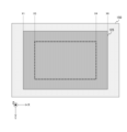
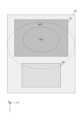
- FIG. 2 is an example of a top view of the semiconductor package 100 according to the first embodiment of the present technology.
- the area of the substrate 150 on the XY plane is larger than the laminated chip 125 .
- an inertial measurement unit 130 (not shown) having a smaller area is stacked on the chip plane below the stacked chip 125 .
- a thick dotted line in the figure indicates the outer circumference of the inertial measurement unit 130 .
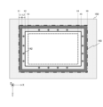
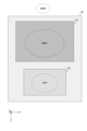
- FIG. 3 is an example of a top view of the substrate 150 according to the first embodiment of the present technology.
- a cavity is formed in the upper substrate plane of the substrate 150 .
- a thick solid line of the rectangle in the figure indicates the outer periphery of the cavity.
- An inertial measurement unit 130 (not shown) is placed in this cavity.
- a thick dotted line in the figure indicates the outer circumference of the inertial measurement unit 130 .
- a ground pattern 143 is formed in the region surrounding the cavity, and a plurality of terminals 142 are formed in the vicinity thereof.
- a ring-shaped ground pattern 143 having a width of L1 is formed along the outer circumference of the control chip 120 .
- a plurality of terminals 142 are formed in a ring-shaped region having a width of L2 inside the ground pattern 143 . Signals and power are supplied through these terminals 142 .
- a certain clearance is provided between the ground pattern 143 and the terminal 142 to avoid short-circuiting.
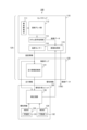
- FIG. 4 is a block diagram showing one configuration example of the semiconductor package 100 according to the first embodiment of the present technology.
- Semiconductor package 100 includes sensor chip 110 , control chip 120 , inertial measurement unit 130 and substrate 150 .
- the sensor chip 110 includes a vertical driving section 111, a pixel array section 112, a column signal processing section 113, a temperature sensor 114 and an image processing section 115.
- a plurality of pixels (not shown) are arranged in a two-dimensional grid in the pixel array section 112 .
- Each pixel generates a pixel signal by photoelectric conversion and supplies it to the column signal processing unit 113 .
- the vertical drive unit 111 drives rows in order to output pixel signals.
- the column signal processing unit 113 performs various kinds of signal processing on pixel signals for each column. As signal processing, AD (Analog to Digital) conversion processing and CDS (Correlated Double Sampling) processing are executed.
- the column signal processing unit 113 supplies the image data in which the processed pixel signals are arranged to the image processing unit 115 .
- This image processing unit 115 may exist in the sensor chip 110 or may exist in the control chip 120 .
- the temperature sensor 114 measures the temperature of a predetermined location on the sensor chip 110 .
- the temperature sensor 114 measures the temperature periodically or at a predetermined timing while a predetermined circuit in the sensor chip 110 is operating, for example.
- Temperature sensor 114 generates and provides temperature information indicative of measurements to control chip 120 and inertial measurement unit 130 .
- the temperature sensor 114 is provided on the sensor chip 110, it is not limited to this configuration.
- the temperature sensor 114 may not be located on the sensor chip 110 but may be located on the control chip 120 instead.
- the image processing unit 115 performs predetermined image processing on the image data from the column signal processing unit 113 .
- the processed image data is supplied to the substrate 150 .
- the image processing unit 115 can perform image processing such as camera shake correction using the inertia information. Image quality of image data is improved by this camera shake correction. In this way, sensor fusion that combines the CMOS image sensor (sensor chip 110) and the inertial measurement unit 130 can realize a sensor with high added value.
- processing using inertial information is not limited to camera shake correction.
- a worker wears a device in which the semiconductor package 100 is mounted, and image data and inertia information from the device are used to recognize and analyze the worker's behavior, thereby improving work.
- the content of this process is, for example, "https://www.researchgate.net/figure/ Illustration-of-the-feature-transforms-for-wearable-sensor-signals_fig3_335319090".
- the moving speed and position information of the worker can be acquired from the inertial information, and the process of three-dimensional modeling of the site where the worker is present can be performed using these and image data.
- the contents of the processing are, for example, "https://unit.aist.go.jp/hiri/cfsr/2011/ symposium0317/kurata20110328.pdf”.
- the sensor chip 110 performs processing using inertial information, it is not limited to this configuration.
- the processing using the inertial information can also be performed by the control chip 120 or circuits in the substrate 150 .
- the processing can be performed by a circuit outside the semiconductor package 100 .
- the control chip 120 has a warp information conversion section 121 .
- the warp information conversion unit 121 converts temperature information into warp information.
- the warp information conversion unit 121 supplies the acquired warp information to the inertial measurement unit 130 .
- the designer obtains the degree of warpage for each temperature by simulation or actual measurement, creates a table describing the warpage information for each temperature, and stores it in a memory (not shown) in the control chip 120 or the like. let me Then, the warp information conversion unit 121 acquires the warp information by reading the warp information corresponding to the temperature from the table. Alternatively, the warp information conversion unit 121 converts temperature information into warp information by performing calculations using a predetermined function that indicates the relationship between temperature and warp.
- warp information conversion unit 121 is arranged in the control chip 120, the configuration is not limited to this.
- the warp information conversion unit 121 can also be arranged on the sensor chip 110 .
- the inertial measurement unit 130 includes MEMS 133 and 134 and a correction circuit 135.
- the MEMS 133 has a movable part 131 and generates inertial information.
- the MEMS 134 has a movable portion 132 and generates inertial information. These MEMS 133 and 134 provide inertial information to correction circuitry 135 . Note that the MEMS 133 and 134 are examples of the inertial sensors described in the claims.
- the correction circuit 135 receives the inertia information from the MEMS 133 and 134 and corrects the inertia information (in other words, drift correction) based on the warp information from the control chip 120 and the temperature information from the sensor chip 110. .
- the correction circuit 135 supplies the corrected inertia information to the image processing section 115 .
- the MEMS 133 and 134 may have the same function, or may have different functions such that one measures acceleration and the other measures angular velocity.
- the correction circuit 135 corrects the inertia information using both the temperature information and the warp information, but is not limited to this configuration, and corrects the inertia information using only the warp information or only the temperature information. You can also
- the laminated chip 125 measures the temperature and estimates the degree of warpage of itself based on the temperature.
- Inertial measurement unit 130 also generates inertial information and corrects the inertial information based on the estimated degree of warpage and temperature. Thereby, the measurement accuracy of the inertial measurement unit 130 can be improved.
- MEMS are arranged in the inertial measurement unit 130, the number of MEMS is not limited to two, and may be one or three or more.
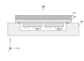
- the semiconductor package 100 may be provided with two or more inertial measurement units such as the inertial measurement units 130-1 and 130-2.
- the position is not limited to the central portion of the chip plane of the control chip 120, and may be a position away from the central portion. In this case, for example, it is desirable to place the inertial measurement unit 130 at one of the following positions. (1) Directly under the circuit block where current consumption of the control chip 120 or the sensor chip 110 concentrates. (2) Directly below the temperature sensor arranged on the control chip 120 or the sensor chip 110; (3) A position that satisfies (1) and (2) at the same time.
- the temperature sensor 114 can transmit accurate temperature information of the heat-generating location to the inertial measurement unit 130 .
- FIG. 7 is a diagram showing an example of temperature distribution on the upper surface of a semiconductor package in a comparative example. As illustrated in the figure, in the comparative example, the laminated chip 125 and the inertial measurement unit 130 are not laminated, and the inertial measurement unit 130 is arranged near the laminated chip 125 on the substrate plane of the substrate 150 .
- the temperature sensor mounted on the layered chip 125 measures 70° C. and supplies it to the inertial measurement unit 130, and the inertial measurement unit 130 corrects the inertial information based on that temperature.
- a deviation occurs between the measured value of the temperature sensor (70° C., etc.) and the actual temperature of the inertial measurement unit 130 (60° C., etc.), and the inertial measurement unit 130 Drift may not be corrected sufficiently.
- the inertial measurement unit 130 can improve the accuracy of drift correction.
- the area of the semiconductor package 100 can be made smaller than the comparative example illustrated in FIG. 7 in the XY plane. can.
- FIG. 8 is a diagram showing an example of the magnitude of vibration on the upper surface of a semiconductor package in a comparative example. It is assumed that vibration occurs at a vibration source near the substrate plane, and the laminated chip 125 is closer to the vibration source than the inertial measurement unit 130 on the substrate plane. In this case, the laminated chips 125 closer to each other have a larger amount of vibration than the inertial measurement unit 130 . For this reason, the amount of correction for camera shake correction based on the inertia information measured by the inertial measurement unit 130 is insufficient, and the correction accuracy of the camera shake correction is reduced.
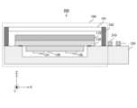
- FIG. 9 is a cross-sectional view showing one configuration example of the sensor module 200 according to the first embodiment of the present technology.
- This sensor module 200 includes a semiconductor package 100 having the structure illustrated in FIG. 1 and a predetermined number of electronic components 210 . Note that the sensor module 200 is an example of the module described in the claims.
- the semiconductor package 100 further includes a frame 192 surrounding the sensor chip 110 and the control chip 120, and glass 191 protecting the top of the sensor chip 110.
- the electronic component 210 is mounted near the semiconductor package 100 .
- a capacitor, a resistor, and a regulator are used as the electronic component 210, for example.
- the inertial measurement unit 130 corrects the inertial information based on the degree of warpage estimated from the temperature and the temperature. Inertial sensor) measurement accuracy can be improved.
- the terminal 142 is arranged near the ground pattern 143, but with this configuration, it is difficult to further reduce the resistance value of the ground pattern 143.
- FIG. The semiconductor package 100 in this modification of the first embodiment differs from the first embodiment in that the width of the ground pattern 143 is increased.
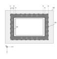
- FIG. 10 is an example of a top view of the substrate 150 in the modified example of the first embodiment of the present technology.
- a ground pattern 143 is formed over the entire area between the outer circumference of the control chip 120 (one-dot chain line) and the outer circumference of the cavity (thick solid line).
- the width of the ground pattern 143 is L1+L2, which is thicker than in the first embodiment. By increasing the width of the ground pattern 143, its resistance value can be reduced.
- a plurality of island-like regions are provided in the ground pattern 143, and the terminals 142 are formed in each region.
- a certain clearance is provided between the periphery of the terminal 142 and the periphery of the island-like region in order to avoid short circuits.
- a ring-shaped gray portion around the terminal 142 in the figure indicates the clearance.
- the portion where the terminal 142 and the ground pattern 143 are provided connects the chip and the substrate so that there is no gap. There is a need to. This is because if there is a gap here, the portion of the inertial measurement unit 130 cannot maintain a vacuum.
- the ground pattern 143 is thickened, so the resistance value can be reduced.
- Second Embodiment> In the first embodiment described above, the inside of the cavity is evacuated to seal the movable parts 131 and 132, but they can also be sealed with a silicon cap.
- the semiconductor package 100 according to the second embodiment differs from the first embodiment in that the movable portion 131 and the like are sealed using a silicon cap.
- FIG. 11 is a cross-sectional view showing one configuration example of the semiconductor package 100 according to the second embodiment of the present technology.
- the semiconductor package 100 of the second embodiment differs from that of the first embodiment in that a silicon cap 136 is further provided.
- the silicon cap 136 seals the movable parts 131 and 132 .
- the inside of this silicon cap 136 is in a vacuum state. Therefore, it is no longer necessary to keep the inside of the cavity in a vacuum state.
- a method for manufacturing the silicon cap 136 is described, for example, in JP-A-2008-288384.
- the modified example of the first embodiment can be applied to the second embodiment.
- the silicon cap 136 seals the movable parts 131 and 132, it is not necessary to create a vacuum state inside the cavity.
- FIG. 12 is a cross-sectional view showing one configuration example of the semiconductor package 100 according to the third embodiment of the present technology.
- the semiconductor package 100 of the third embodiment differs from the first embodiment in that dummy silicon 160 is further arranged.
- the dummy silicon 160 is a member made of silicon on which no circuit or element is provided. This dummy silicon 160 is arranged in the area exposed in the cavity in the chip plane under the control chip 120 .
- the dummy silicon 160 By mounting the dummy silicon 160, even if the inertial measurement unit 130 is not arranged in the central portion, the balance of stress on the layered chip 125 can be improved and the warping of the layered chip 125 can be suppressed. In addition, by conducting heat through the dummy silicon 160 , the heat distribution of the layered chip 125 can be diffused, and heat concentration on the inertial measurement unit 130 can be suppressed.
- the modified example of the first embodiment and the second embodiment can be applied to the third embodiment.
- the dummy silicon 160 is further arranged, warping of the laminated chip 125 and concentration of heat on the inertial measurement unit 130 can be suppressed.
- the sensor chip 110 and the substrate 150 are not connected in the first embodiment described above, they can be electrically connected.
- the semiconductor package 100 of the fourth embodiment differs from that of the first embodiment in that the sensor chip 110 and the substrate 150 are joined by wires.
- FIG. 13 is a cross-sectional view showing one configuration example of the semiconductor package 100 according to the fourth embodiment of the present technology.
- a predetermined number of pads 144 are formed on the substrate 150 and a predetermined number of pads 145 are formed on the sensor chip 110 .
- These pads 144 and 145 are joined by wires. This wire bonding electrically connects the sensor chip 110 and the substrate 150 .
- the control chip 120 can be connected to the substrate 150 by wires. In this case, it is necessary to make the area of the sensor chip 110 smaller than that of the control chip 120 to secure the space for the pad 145 . Also, when the control chip 120 is connected by wire, as illustrated in FIG. 10, a ground pattern 143 can be formed on the entire surface between the outer periphery of the control chip 120 and the outer periphery of the cavity. However, although the terminals 142 are arranged in the ground pattern 143 in FIG. 10, the terminals 142 may not be arranged when the control chip 120 is connected by wires.
- the second embodiment and the third embodiment can be applied to the fourth embodiment.
- the sensor chip 110 and the substrate 150 are joined by wires, so that they can be electrically connected.
- control chip 120 and the substrate 150 are connected by the terminals 141 and 142.
- thermocompression bonding or the like which requires thermal energy and mechanical force. energy is required.
- the semiconductor package 100 in the modified example of the fourth embodiment differs from the fourth embodiment in that the control chip 120 and the substrate 150 are connected by resin.
- FIG. 15 is a cross-sectional view showing one configuration example of the semiconductor package 100 according to the modification of the fourth embodiment of the present technology.
- This modification of the fourth embodiment differs from the fourth embodiment in that the control chip 120 and the substrate 150 are connected by a resin 146 that functions as an adhesive.
- the connection by the resin 146 eliminates the need for thermocompression bonding and the like, and can reduce thermal energy and mechanical energy required for connection.
- control chip 120 and the substrate 150 are connected by the resin 146, so the energy required for connection can be reduced.
- the control chip 120 is connected to the substrate 150.
- the heat generated by the sensor chip 110 and the control chip 120 is also conducted to the substrate, and the substrate 150 is damaged due to the difference in the coefficient of thermal expansion. It may warp.
- the semiconductor package 100 according to the fifth embodiment differs from the first embodiment in that a metal plate is attached to the substrate 150 .
- FIG. 16 is a cross-sectional view showing one configuration example of the semiconductor package 100 according to the fifth embodiment of the present technology.
- the semiconductor package 100 of the fifth embodiment differs from the first embodiment in that a metal plate 170 is further provided.
- the metal plate 170 is attached to the bottom surface of the substrate 150 .
- a plate with high hardness such as a stainless steel (SUS: Steel Use Stainless) plate is used. Bonding the metal plate 170 can suppress warpage of the substrate 150 due to temperature fluctuations.
- the metal plate 170 is attached to the substrate 150, warping of the substrate 150 can be suppressed.
- the technology (the present technology) according to the present disclosure can be applied to various products.
- the technology according to the present disclosure can be realized as a device mounted on any type of moving body such as automobiles, electric vehicles, hybrid electric vehicles, motorcycles, bicycles, personal mobility, airplanes, drones, ships, and robots. may
- FIG. 17 is a block diagram showing a schematic configuration example of a vehicle control system, which is an example of a mobile control system to which the technology according to the present disclosure can be applied.
- a vehicle control system 12000 includes a plurality of electronic control units connected via a communication network 12001.
- the vehicle control system 12000 includes a drive system control unit 12010, a body system control unit 12020, an exterior information detection unit 12030, an interior information detection unit 12040, and an integrated control unit 12050.
- a microcomputer 12051, an audio/image output section 12052, and an in-vehicle network I/F (interface) 12053 are illustrated.
- the drive system control unit 12010 controls the operation of devices related to the drive system of the vehicle according to various programs.
- the driving system control unit 12010 includes a driving force generator for generating driving force of the vehicle such as an internal combustion engine or a driving motor, a driving force transmission mechanism for transmitting the driving force to the wheels, and a steering angle of the vehicle. It functions as a control device such as a steering mechanism to adjust and a brake device to generate braking force of the vehicle.
- the body system control unit 12020 controls the operation of various devices equipped on the vehicle body according to various programs.
- the body system control unit 12020 functions as a keyless entry system, a smart key system, a power window device, or a control device for various lamps such as headlamps, back lamps, brake lamps, winkers or fog lamps.
- body system control unit 12020 can receive radio waves transmitted from a portable device that substitutes for a key or signals from various switches.
- the body system control unit 12020 receives the input of these radio waves or signals and controls the door lock device, power window device, lamps, etc. of the vehicle.
- the vehicle exterior information detection unit 12030 detects information outside the vehicle in which the vehicle control system 12000 is installed.
- the vehicle exterior information detection unit 12030 is connected with an imaging section 12031 .
- the vehicle exterior information detection unit 12030 causes the imaging unit 12031 to capture an image of the exterior of the vehicle, and receives the captured image.
- the vehicle exterior information detection unit 12030 may perform object detection processing or distance detection processing such as people, vehicles, obstacles, signs, or characters on the road surface based on the received image.
- the imaging unit 12031 is an optical sensor that receives light and outputs an electrical signal according to the amount of received light.
- the imaging unit 12031 can output the electric signal as an image, and can also output it as distance measurement information.
- the light received by the imaging unit 12031 may be visible light or non-visible light such as infrared rays.
- the in-vehicle information detection unit 12040 detects in-vehicle information.
- the in-vehicle information detection unit 12040 is connected to, for example, a driver state detection section 12041 that detects the state of the driver.
- the driver state detection unit 12041 includes, for example, a camera that captures an image of the driver, and the in-vehicle information detection unit 12040 detects the degree of fatigue or concentration of the driver based on the detection information input from the driver state detection unit 12041. It may be calculated, or it may be determined whether the driver is dozing off.
- the microcomputer 12051 calculates control target values for the driving force generator, the steering mechanism, or the braking device based on the information inside and outside the vehicle acquired by the vehicle exterior information detection unit 12030 or the vehicle interior information detection unit 12040, and controls the drive system control unit.
- a control command can be output to 12010 .
- the microcomputer 12051 realizes the functions of ADAS (Advanced Driver Assistance System) including collision avoidance or shock mitigation, follow-up driving based on inter-vehicle distance, vehicle speed maintenance driving, vehicle collision warning, or vehicle lane deviation warning. Cooperative control can be performed for the purpose of ADAS (Advanced Driver Assistance System) including collision avoidance or shock mitigation, follow-up driving based on inter-vehicle distance, vehicle speed maintenance driving, vehicle collision warning, or vehicle lane deviation warning. Cooperative control can be performed for the purpose of ADAS (Advanced Driver Assistance System) including collision avoidance or shock mitigation, follow-up driving based on inter-vehicle distance, vehicle speed maintenance driving, vehicle collision warning, or vehicle
- the microcomputer 12051 controls the driving force generator, the steering mechanism, the braking device, etc. based on the information about the vehicle surroundings acquired by the vehicle exterior information detection unit 12030 or the vehicle interior information detection unit 12040, so that the driver's Cooperative control can be performed for the purpose of autonomous driving, etc., in which vehicles autonomously travel without depending on operation.
- the microcomputer 12051 can output a control command to the body system control unit 12020 based on the information outside the vehicle acquired by the information detection unit 12030 outside the vehicle.
- the microcomputer 12051 controls the headlamps according to the position of the preceding vehicle or the oncoming vehicle detected by the vehicle exterior information detection unit 12030, and performs cooperative control aimed at anti-glare such as switching from high beam to low beam. It can be carried out.
- the audio/image output unit 12052 transmits at least one of audio and/or image output signals to an output device capable of visually or audibly notifying the passengers of the vehicle or the outside of the vehicle.
- an audio speaker 12061, a display unit 12062, and an instrument panel 12063 are illustrated as output devices.
- the display unit 12062 may include at least one of an on-board display and a head-up display, for example.
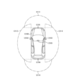
- FIG. 18 is a diagram showing an example of the installation position of the imaging unit 12031.
- the imaging unit 12031 has imaging units 12101, 12102, 12103, 12104, and 12105.
- the imaging units 12101, 12102, 12103, 12104, and 12105 are provided at positions such as the front nose of the vehicle 12100, the side mirrors, the rear bumper, the back door, and the upper part of the windshield in the vehicle interior, for example.
- An image pickup unit 12101 provided in the front nose and an image pickup unit 12105 provided above the windshield in the passenger compartment mainly acquire images in front of the vehicle 12100 .
- Imaging units 12102 and 12103 provided in the side mirrors mainly acquire side images of the vehicle 12100 .
- An imaging unit 12104 provided in the rear bumper or back door mainly acquires an image behind the vehicle 12100 .
- the imaging unit 12105 provided above the windshield in the passenger compartment is mainly used for detecting preceding vehicles, pedestrians, obstacles, traffic lights, traffic signs, lanes, and the like.
- FIG. 18 shows an example of the imaging range of the imaging units 12101 to 12104.
- the imaging range 12111 indicates the imaging range of the imaging unit 12101 provided in the front nose
- the imaging ranges 12112 and 12113 indicate the imaging ranges of the imaging units 12102 and 12103 provided in the side mirrors, respectively
- the imaging range 12114 The imaging range of an imaging unit 12104 provided in the rear bumper or back door is shown. For example, by superimposing the image data captured by the imaging units 12101 to 12104, a bird's-eye view image of the vehicle 12100 viewed from above can be obtained.
- At least one of the imaging units 12101 to 12104 may have a function of acquiring distance information.
- at least one of the imaging units 12101 to 12104 may be a stereo camera composed of a plurality of imaging elements, or may be an imaging element having pixels for phase difference detection.
- the microcomputer 12051 determines the distance to each three-dimensional object within the imaging ranges 12111 to 12114 and changes in this distance over time (relative velocity with respect to the vehicle 12100). , it is possible to extract, as the preceding vehicle, the closest three-dimensional object on the course of the vehicle 12100, which runs at a predetermined speed (for example, 0 km/h or more) in substantially the same direction as the vehicle 12100. can. Furthermore, the microcomputer 12051 can set the inter-vehicle distance to be secured in advance in front of the preceding vehicle, and perform automatic brake control (including following stop control) and automatic acceleration control (including following start control). In this way, cooperative control can be performed for the purpose of automatic driving in which the vehicle runs autonomously without relying on the operation of the driver.
- automatic brake control including following stop control
- automatic acceleration control including following start control
- the microcomputer 12051 converts three-dimensional object data related to three-dimensional objects to other three-dimensional objects such as motorcycles, ordinary vehicles, large vehicles, pedestrians, and utility poles. It can be classified and extracted and used for automatic avoidance of obstacles. For example, the microcomputer 12051 distinguishes obstacles around the vehicle 12100 into those that are visible to the driver of the vehicle 12100 and those that are difficult to see. Then, the microcomputer 12051 judges the collision risk indicating the degree of danger of collision with each obstacle, and when the collision risk is equal to or higher than the set value and there is a possibility of collision, an audio speaker 12061 and a display unit 12062 are displayed. By outputting an alarm to the driver via the drive system control unit 12010 and performing forced deceleration and avoidance steering via the drive system control unit 12010, driving support for collision avoidance can be performed.
- At least one of the imaging units 12101 to 12104 may be an infrared camera that detects infrared rays.
- the microcomputer 12051 can recognize a pedestrian by determining whether or not the pedestrian exists in the captured images of the imaging units 12101 to 12104 .
- recognition of a pedestrian is performed by, for example, a procedure for extracting feature points in images captured by the imaging units 12101 to 12104 as infrared cameras, and performing pattern matching processing on a series of feature points indicating the outline of an object to determine whether or not the pedestrian is a pedestrian.
- the audio image output unit 12052 outputs a rectangular outline for emphasis to the recognized pedestrian. is superimposed on the display unit 12062 . Also, the audio/image output unit 12052 may control the display unit 12062 to display an icon or the like indicating a pedestrian at a desired position.
- the technology according to the present disclosure can be applied to the imaging unit 12031 among the configurations described above.
- the semiconductor package 100 in FIG. 1 can be applied to the imaging unit 12031 .
- the present technology can also have the following configuration.
- a laminated chip that measures temperature and estimates the degree of warpage of itself from the temperature;
- a semiconductor package comprising: a measurement unit that performs a process of measuring a predetermined physical quantity to generate measurement information and a process of correcting the measurement information based on the degree of warpage.
- the measurement unit corrects the measurement information based on the temperature and the degree of warpage.
- the measurement unit an inertial sensor having a movable portion exposed in the cavity and generating inertial information as the measurement information;
- the semiconductor package according to (10), wherein the measurement unit further includes a silicon cap that seals the movable portion.
- the laminated chip includes a sensor chip that generates image data.
- semiconductor package 110 sensor chip 111 vertical drive section 112 pixel array section 113 column signal processing section 114 temperature sensor 115 image processing section 120 control chip 121 warp information conversion section 125 laminated chip 130, 130-1, 130-2 inertial measurement unit 131 , 132 movable part 133, 134 MEMS 135 correction circuit 136 silicon cap 141, 142 terminal 143 ground pattern 144, 145 pad 146 resin 150 substrate 160 dummy silicon 170 metal plate 191 glass 192 frame 200 sensor module 210 electronic component 12031 imaging unit
Landscapes
- Physics & Mathematics (AREA)
- General Physics & Mathematics (AREA)
- Gyroscopes (AREA)
Abstract
Description
1.第1の実施の形態(慣性情報をドリフト補正する例)
2.第2の実施の形態(シリコンキャップにより可動部を封止し、慣性情報をドリフト補正する例)
3.第3の実施の形態(ダミーシリコンを配置し、慣性情報をドリフト補正する例)
4.第4の実施の形態(ワイヤーにより接合し、慣性情報をドリフト補正する例)
5.第5の実施の形態(金属板を基板に貼り付け、慣性情報をドリフト補正する例)
6.移動体への応用例
[半導体パッケージの構成例]
図1は、本技術の第1の実施の形態における半導体パッケージ100の一構成例を示す断面図である。この半導体パッケージ100は、撮像装置などに搭載されるパッケージであり、積層チップ125、慣性計測ユニット(IMU:Inertial Measurement Unit)130および基板150を備える。積層チップ125は、積層されたセンサチップ110および制御チップ120を含む。なお、半導体パッケージ100は、積層チップ125を保護するためのフレームやガラスをさらに備えるが、これらは、同図において両略されている。
Illustration-of-the-feature-transforms-for-wearable-sensor-signals_fig3_335319090」に記載されている。あるいは、慣性情報から、作業員の移動速度や位置情報を取得し、それらと画像データとを用いて、作業員のいる現場を3次元モデリングする処理を行うこともできる。その処理内容は、例えば、「https://unit.aist.go.jp/hiri/cfsr/2011/
symposium0317/kurata20110328.pdf」に記載されている。
(1)制御チップ120あるいはセンサチップ110の消費電流が集中する回路ブロックの直下。
(2)制御チップ120あるいはセンサチップ110に配置された温度センサーの直下。
(3)(1)と(2)とを同時に満たす位置。
図9は、本技術の第1の実施の形態におけるセンサモジュール200の一構成例を示す断面図である。このセンサモジュール200は、図1に例示した構造の半導体パッケージ100と、所定数の電子部品210とを備える。なお、センサモジュール200は、特許請求の範囲に記載のモジュールの一例である。
上述の第1の実施の形態では、グランドパターン143の近傍に端子142を配置していたが、この構成では、グランドパターン143の抵抗値をさらに低減することが困難である。この第1の実施の形態の変形例における半導体パッケージ100は、グランドパターン143の幅を太くした点において第1の実施の形態と異なる。
上述の第1の実施の形態では、キャビティ内を真空にして可動部131や132を封止していたが、それらをシリコンキャップにより封止することもできる。この第2の実施の形態における半導体パッケージ100は、シリコンキャップを用いて可動部131などを封止する点において第1の実施の形態と異なる。
上述の第1の実施の形態では、キャビティ内に慣性計測ユニット130のみを配置していた。しかし、図6に例示したように慣性計測ユニット130を中央部に配置しない場合、制御チップ120の反りや、慣性計測ユニット130への熱の集中を十分に抑制することができないことがある。この第3の実施の形態の半導体パッケージ100は、反りや、熱の集中を抑制する目的でダミーシリコンをさらに配置した点において第1の実施の形態と異なる。
上述の第1の実施の形態では、センサチップ110と基板150とを接続していなかったが、これらを電気的に接続することもできる。この第4の実施の形態の半導体パッケージ100は、センサチップ110と基板150とをワイヤーにより接合した点において第1の実施の形態と異なる。
上述の第4の実施の形態では、制御チップ120と基板150とを端子141や142により接続していたが、端子同士を接合するには、熱圧着などを行う必要があり、熱エネルギーや機械的エネルギーが必要になる。この第4の実施の形態の変形例における半導体パッケージ100は、制御チップ120と基板150とを樹脂により接続した点において第4の実施の形態と異なる。
上述の第1の実施の形態では、基板150に制御チップ120を接続していたが、センサチップ110や制御チップ120で生じた熱が基板にも伝導し、熱膨張率の相違により基板150が反ってしまうおそれがある。この第5の実施の形態における半導体パッケージ100は、金属板を基板150に貼り付けた点において第1の実施の形態と異なる。
本開示に係る技術(本技術)は、様々な製品へ応用することができる。例えば、本開示に係る技術は、自動車、電気自動車、ハイブリッド電気自動車、自動二輪車、自転車、パーソナルモビリティ、飛行機、ドローン、船舶、ロボット等のいずれかの種類の移動体に搭載される装置として実現されてもよい。
(1)温度を測定して前記温度から自身の反りの程度を推定する積層チップと、
所定の物理量を測定して測定情報を生成する処理と前記反りの程度に基づいて前記測定情報を補正する処理とを行う計測ユニットと
を具備する半導体パッケージ。
(2)前記計測ユニットは、前記温度と前記反りの程度とに基づいて前記測定情報を補正する
前記(1)記載の半導体パッケージ。
(3)所定の基板平面にキャビティが形成された基板をさらに具備し、
前記積層チップのチップ平面は、前記基板平面のうち前記キャビティの周囲の所定領域に接続され、
前記計測ユニットは、前記チップ平面のうち前記キャビティ内に露出した領域に配置される
前記(1)または(2)に記載の半導体パッケージ。
(4)前記基板平面のうち前記キャビティの周囲の所定領域には、グランドパターンと前記グランドパターンの近傍に配置された端子とが配置される
前記(3)記載の半導体パッケージ。
(5)前記基板平面のうち前記キャビティの周囲の所定領域には、アイランド状の領域を含むグランドパターンと前記アイランド状の領域内に形成された端子とが配置される
前記(3)記載の半導体パッケージ。
(6)前記チップ平面のうち前記キャビティ内に露出した領域に配置されたダミーシリコンをさらに具備する
前記(3)から(5)のいずれかに記載の半導体パッケージ。
(7)前記積層チップは、積層された複数のチップを含み、
前記複数のチップのいずれかと前記基板とはワイヤーにより接合される
前記(3)から(6)のいずれかに記載の半導体パッケージ。
(8)前記積層チップと前記基板とは、樹脂により接続される
前記(3)から(7)のいずれかに記載の半導体パッケージ。
(9)前記基板に貼り付けられた金属板をさらに具備する
前記(3)から(8)のいずれかに記載の半導体パッケージ。
(10)前記計測ユニットは、
可動部が前記キャビティ内に露出し、前記測定情報として慣性情報を生成する慣性センサーと、
前記反りの程度に基づいて前記慣性情報を補正する補正回路と
を備える
前記(3)から(9)のいずれに記載の半導体パッケージ。
(11)前記計測ユニットは、前記可動部を封止するシリコンキャップをさらに備える
前記(10)記載の半導体パッケージ。
(12)前記積層チップは、画像データを生成するセンサチップを含む
前記(1)から(11)のいずれかに記載の半導体パッケージ。
(13)前記センサチップは、前記補正された測定情報を用いて前記画像データを処理する
前記(12)記載の半導体パッケージ。
(14)温度を測定して前記温度から自身の反りの程度を推定する積層チップと、
所定の物理量を測定して測定情報を生成する処理と前記反りの程度に基づいて前記測定情報を補正する処理とを行う計測ユニットと
を具備するモジュール。
110 センサチップ
111 垂直駆動部
112 画素アレイ部
113 カラム信号処理部
114 温度センサー
115 画像処理部
120 制御チップ
121 反り情報変換部
125 積層チップ
130、130-1、130-2 慣性計測ユニット
131、132 可動部
133、134 MEMS
135 補正回路
136 シリコンキャップ
141、142 端子
143 グランドパターン
144、145 パッド
146 樹脂
150 基板
160 ダミーシリコン
170 金属板
191 ガラス
192 フレーム
200 センサモジュール
210 電子部品
12031 撮像部
Claims (14)
- 温度を測定して前記温度から自身の反りの程度を推定する積層チップと、
所定の物理量を測定して測定情報を生成する処理と前記反りの程度に基づいて前記測定情報を補正する処理とを行う計測ユニットと
を具備する半導体パッケージ。 - 前記計測ユニットは、前記温度と前記反りの程度とに基づいて前記測定情報を補正する
請求項1記載の半導体パッケージ。 - 所定の基板平面にキャビティが形成された基板をさらに具備し、
前記積層チップのチップ平面は、前記基板平面のうち前記キャビティの周囲の所定領域に接続され、
前記計測ユニットは、前記チップ平面のうち前記キャビティ内に露出した領域に配置される
請求項1記載の半導体パッケージ。 - 前記基板平面のうち前記キャビティの周囲の所定領域には、グランドパターンと前記グランドパターンの近傍に配置された端子とが配置される
請求項3記載の半導体パッケージ。 - 前記基板平面のうち前記キャビティの周囲の所定領域には、アイランド状の領域を含むグランドパターンと前記アイランド状の領域内に形成された端子とが配置される
請求項3記載の半導体パッケージ。 - 前記チップ平面のうち前記キャビティ内に露出した領域に配置されたダミーシリコンをさらに具備する
請求項3記載の半導体パッケージ。 - 前記積層チップは、積層された複数のチップを含み、
前記複数のチップのいずれかと前記基板とはワイヤーにより接合される
請求項3記載の半導体パッケージ。 - 前記積層チップと前記基板とは、樹脂により接続される
請求項3記載の半導体パッケージ。 - 前記基板に貼り付けられた金属板をさらに具備する
請求項3記載の半導体パッケージ。 - 前記計測ユニットは、
可動部が前記キャビティ内に露出し、前記測定情報として慣性情報を生成する慣性センサーと、
前記反りの程度に基づいて前記慣性情報を補正する補正回路と
を備える
請求項3記載の半導体パッケージ。 - 前記計測ユニットは、前記可動部を封止するシリコンキャップをさらに備える
請求項10記載の半導体パッケージ。 - 前記積層チップは、画像データを生成するセンサチップを含む
請求項1記載の半導体パッケージ。 - 前記センサチップは、前記補正された測定情報を用いて前記画像データを処理する
請求項12記載の半導体パッケージ。 - 温度を測定して前記温度から自身の反りの程度を推定する積層チップと、
所定の物理量を測定して測定情報を生成する処理と前記反りの程度に基づいて前記測定情報を補正する処理とを行う計測ユニットと
を具備するモジュール。
Priority Applications (2)
| Application Number | Priority Date | Filing Date | Title |
|---|---|---|---|
| CN202280068483.1A CN118103977A (zh) | 2021-11-25 | 2022-09-30 | 半导体封装件和模块 |
| US18/710,284 US20250251238A1 (en) | 2021-11-25 | 2022-09-30 | Semiconductor package and module |
Applications Claiming Priority (2)
| Application Number | Priority Date | Filing Date | Title |
|---|---|---|---|
| JP2021-190665 | 2021-11-25 | ||
| JP2021190665 | 2021-11-25 |
Publications (1)
| Publication Number | Publication Date |
|---|---|
| WO2023095443A1 true WO2023095443A1 (ja) | 2023-06-01 |
Family
ID=86539249
Family Applications (1)
| Application Number | Title | Priority Date | Filing Date |
|---|---|---|---|
| PCT/JP2022/036689 Ceased WO2023095443A1 (ja) | 2021-11-25 | 2022-09-30 | 半導体パッケージ、および、モジュール |
Country Status (3)
| Country | Link |
|---|---|
| US (1) | US20250251238A1 (ja) |
| CN (1) | CN118103977A (ja) |
| WO (1) | WO2023095443A1 (ja) |
Citations (4)
| Publication number | Priority date | Publication date | Assignee | Title |
|---|---|---|---|---|
| JP2005257504A (ja) * | 2004-03-12 | 2005-09-22 | Nippon Soken Inc | 物理量センサ装置 |
| JP2012088194A (ja) * | 2010-10-20 | 2012-05-10 | Denso Corp | 容量式物理量検出装置 |
| WO2018074230A1 (ja) * | 2016-10-18 | 2018-04-26 | ソニーセミコンダクタソリューションズ株式会社 | チップモジュールおよびその信号処理方法、並びに、電子機器 |
| WO2021009970A1 (ja) * | 2019-07-17 | 2021-01-21 | 株式会社村田製作所 | 半導体モジュール |
-
2022
- 2022-09-30 CN CN202280068483.1A patent/CN118103977A/zh active Pending
- 2022-09-30 US US18/710,284 patent/US20250251238A1/en active Pending
- 2022-09-30 WO PCT/JP2022/036689 patent/WO2023095443A1/ja not_active Ceased
Patent Citations (4)
| Publication number | Priority date | Publication date | Assignee | Title |
|---|---|---|---|---|
| JP2005257504A (ja) * | 2004-03-12 | 2005-09-22 | Nippon Soken Inc | 物理量センサ装置 |
| JP2012088194A (ja) * | 2010-10-20 | 2012-05-10 | Denso Corp | 容量式物理量検出装置 |
| WO2018074230A1 (ja) * | 2016-10-18 | 2018-04-26 | ソニーセミコンダクタソリューションズ株式会社 | チップモジュールおよびその信号処理方法、並びに、電子機器 |
| WO2021009970A1 (ja) * | 2019-07-17 | 2021-01-21 | 株式会社村田製作所 | 半導体モジュール |
Also Published As
| Publication number | Publication date |
|---|---|
| US20250251238A1 (en) | 2025-08-07 |
| CN118103977A (zh) | 2024-05-28 |
Similar Documents
| Publication | Publication Date | Title |
|---|---|---|
| JP7499242B2 (ja) | 半導体パッケージ、および、電子装置 | |
| WO2018030139A1 (ja) | 撮像素子パッケージおよびカメラモジュール | |
| US11670625B2 (en) | Imaging unit having a stacked structure and electronic apparatus including the imaging unit | |
| US20240063244A1 (en) | Semiconductor package, electronic device, and method of manufacturing semiconductor package | |
| JP7462620B2 (ja) | 半導体パッケージ、半導体パッケージの製造方法、および、電子装置 | |
| WO2023095443A1 (ja) | 半導体パッケージ、および、モジュール | |
| US20250194292A1 (en) | Semiconductor device | |
| JP7630428B2 (ja) | 半導体パッケージ | |
| WO2019198385A1 (ja) | 撮像装置およびその製造方法、電子機器 | |
| US12255170B2 (en) | Semiconductor package, electronic apparatus, and method for manufacturing semiconductor package | |
| WO2023007797A1 (ja) | 固体撮像素子、撮像装置、および電子機器 | |
| WO2024185282A1 (ja) | 半導体パッケージ、半導体装置、および、半導体パッケージの製造方法 | |
| WO2026018560A1 (ja) | 半導体パッケージ、半導体装置、および、半導体パッケージの製造方法 | |
| WO2024057709A1 (ja) | 半導体パッケージ、および、電子装置 | |
| WO2024106011A1 (ja) | 半導体パッケージ、電子装置、および、半導体パッケージの制御方法 | |
| WO2025158775A1 (ja) | 半導体パッケージ、半導体装置、および、半導体パッケージの製造方法 | |
| WO2024224807A1 (ja) | 半導体パッケージ、および、半導体パッケージの製造方法 | |
| KR20260021703A (ko) | 반도체 패키지, 및 반도체 패키지의 제조 방법 | |
| WO2024075398A1 (ja) | カメラモジュール、および、撮像装置 | |
| WO2025115400A1 (ja) | 半導体パッケージ、半導体装置、および、半導体パッケージの製造方法 | |
| WO2024122177A1 (ja) | 半導体パッケージ、および、半導体パッケージの製造方法 | |
| WO2024241700A1 (ja) | 光学パッケージおよび光学パッケージの製造方法 | |
| WO2026004347A1 (ja) | 光学パッケージ、モジュール、および、光学パッケージの製造方法 | |
| WO2022168514A1 (ja) | 半導体装置、撮像装置 | |
| CN121079769A (zh) | 半导体封装、半导体装置及用于制造半导体封装的方法 |
Legal Events
| Date | Code | Title | Description |
|---|---|---|---|
| 121 | Ep: the epo has been informed by wipo that ep was designated in this application |
Ref document number: 22898228 Country of ref document: EP Kind code of ref document: A1 |
|
| WWE | Wipo information: entry into national phase |
Ref document number: 202280068483.1 Country of ref document: CN |
|
| WWE | Wipo information: entry into national phase |
Ref document number: 18710284 Country of ref document: US |
|
| NENP | Non-entry into the national phase |
Ref country code: DE |
|
| 122 | Ep: pct application non-entry in european phase |
Ref document number: 22898228 Country of ref document: EP Kind code of ref document: A1 |
|
| NENP | Non-entry into the national phase |
Ref country code: JP |
|
| WWP | Wipo information: published in national office |
Ref document number: 18710284 Country of ref document: US |