WO2023095287A1 - Structure, quantum bit, quantum computing device, and method for manufacturing structure - Google Patents
Structure, quantum bit, quantum computing device, and method for manufacturing structure Download PDFInfo
- Publication number
- WO2023095287A1 WO2023095287A1 PCT/JP2021/043410 JP2021043410W WO2023095287A1 WO 2023095287 A1 WO2023095287 A1 WO 2023095287A1 JP 2021043410 W JP2021043410 W JP 2021043410W WO 2023095287 A1 WO2023095287 A1 WO 2023095287A1
- Authority
- WO
- WIPO (PCT)
- Prior art keywords
- layer
- hinge
- helical channel
- groove
- substrate
- Prior art date
Links
- 239000002096 quantum dot Substances 0.000 title claims description 46
- 238000000034 method Methods 0.000 title claims description 38
- 238000004519 manufacturing process Methods 0.000 title claims description 23
- 229910052723 transition metal Inorganic materials 0.000 claims abstract description 16
- 150000003624 transition metals Chemical class 0.000 claims abstract description 16
- JPIIVHIVGGOMMV-UHFFFAOYSA-N ditellurium Chemical compound [Te]=[Te] JPIIVHIVGGOMMV-UHFFFAOYSA-N 0.000 claims abstract description 13
- 239000002887 superconductor Substances 0.000 claims description 196
- 239000012212 insulator Substances 0.000 claims description 117
- 239000000758 substrate Substances 0.000 claims description 85
- 230000005294 ferromagnetic effect Effects 0.000 claims description 43
- 230000005291 magnetic effect Effects 0.000 claims description 11
- 230000004907 flux Effects 0.000 claims description 9
- 230000008859 change Effects 0.000 claims description 8
- 229910052763 palladium Inorganic materials 0.000 claims description 7
- 229910052758 niobium Inorganic materials 0.000 claims description 6
- 230000008569 process Effects 0.000 claims description 5
- 229910052741 iridium Inorganic materials 0.000 claims description 4
- 229910052742 iron Inorganic materials 0.000 claims description 4
- 229910052750 molybdenum Inorganic materials 0.000 claims description 4
- 238000005240 physical vapour deposition Methods 0.000 claims description 4
- 229910052697 platinum Inorganic materials 0.000 claims description 4
- 229910052715 tantalum Inorganic materials 0.000 claims description 4
- 229910052719 titanium Inorganic materials 0.000 claims description 4
- 229910052721 tungsten Inorganic materials 0.000 claims description 4
- 229910052726 zirconium Inorganic materials 0.000 claims description 4
- 229910052782 aluminium Inorganic materials 0.000 claims description 3
- 239000010410 layer Substances 0.000 description 524
- 230000004888 barrier function Effects 0.000 description 25
- 239000000463 material Substances 0.000 description 25
- 241000121629 Majorana Species 0.000 description 16
- 238000005259 measurement Methods 0.000 description 16
- 239000002245 particle Substances 0.000 description 16
- 238000001069 Raman spectroscopy Methods 0.000 description 15
- 238000010894 electron beam technology Methods 0.000 description 14
- 238000000151 deposition Methods 0.000 description 11
- 230000008021 deposition Effects 0.000 description 9
- 238000010586 diagram Methods 0.000 description 8
- 239000002356 single layer Substances 0.000 description 7
- OKKJLVBELUTLKV-UHFFFAOYSA-N Methanol Chemical compound OC OKKJLVBELUTLKV-UHFFFAOYSA-N 0.000 description 6
- 229910004298 SiO 2 Inorganic materials 0.000 description 6
- 238000000992 sputter etching Methods 0.000 description 6
- 239000013078 crystal Substances 0.000 description 5
- 238000007865 diluting Methods 0.000 description 5
- 238000000609 electron-beam lithography Methods 0.000 description 5
- 229910052751 metal Inorganic materials 0.000 description 5
- 239000002184 metal Substances 0.000 description 5
- 238000000137 annealing Methods 0.000 description 4
- QVGXLLKOCUKJST-UHFFFAOYSA-N atomic oxygen Chemical compound [O] QVGXLLKOCUKJST-UHFFFAOYSA-N 0.000 description 4
- 229910052760 oxygen Inorganic materials 0.000 description 4
- 239000001301 oxygen Substances 0.000 description 4
- 238000012545 processing Methods 0.000 description 4
- 238000007740 vapor deposition Methods 0.000 description 4
- 230000001133 acceleration Effects 0.000 description 3
- 238000010549 co-Evaporation Methods 0.000 description 3
- 239000004020 conductor Substances 0.000 description 3
- 230000005684 electric field Effects 0.000 description 3
- 238000011065 in-situ storage Methods 0.000 description 3
- 230000003647 oxidation Effects 0.000 description 3
- 238000007254 oxidation reaction Methods 0.000 description 3
- 238000004544 sputter deposition Methods 0.000 description 3
- 230000015572 biosynthetic process Effects 0.000 description 2
- 238000010790 dilution Methods 0.000 description 2
- 239000012895 dilution Substances 0.000 description 2
- 230000000694 effects Effects 0.000 description 2
- 239000010445 mica Substances 0.000 description 2
- 229910052618 mica group Inorganic materials 0.000 description 2
- 229910003465 moissanite Inorganic materials 0.000 description 2
- 229910052594 sapphire Inorganic materials 0.000 description 2
- 239000010980 sapphire Substances 0.000 description 2
- 239000004065 semiconductor Substances 0.000 description 2
- 229910010271 silicon carbide Inorganic materials 0.000 description 2
- 238000011282 treatment Methods 0.000 description 2
- 229910021642 ultra pure water Inorganic materials 0.000 description 2
- 239000012498 ultrapure water Substances 0.000 description 2
- 229910052582 BN Inorganic materials 0.000 description 1
- PZNSFCLAULLKQX-UHFFFAOYSA-N Boron nitride Chemical compound N#B PZNSFCLAULLKQX-UHFFFAOYSA-N 0.000 description 1
- OKTJSMMVPCPJKN-UHFFFAOYSA-N Carbon Chemical compound [C] OKTJSMMVPCPJKN-UHFFFAOYSA-N 0.000 description 1
- 239000000470 constituent Substances 0.000 description 1
- 238000005421 electrostatic potential Methods 0.000 description 1
- 229910021389 graphene Inorganic materials 0.000 description 1
- CPLXHLVBOLITMK-UHFFFAOYSA-N magnesium oxide Inorganic materials [Mg]=O CPLXHLVBOLITMK-UHFFFAOYSA-N 0.000 description 1
- 239000000395 magnesium oxide Substances 0.000 description 1
- 238000012986 modification Methods 0.000 description 1
- 230000004048 modification Effects 0.000 description 1
- 238000011160 research Methods 0.000 description 1
- 238000012827 research and development Methods 0.000 description 1
- 239000000126 substance Substances 0.000 description 1
- 238000006467 substitution reaction Methods 0.000 description 1
Images


Classifications
-
- H—ELECTRICITY
- H10—SEMICONDUCTOR DEVICES; ELECTRIC SOLID-STATE DEVICES NOT OTHERWISE PROVIDED FOR
- H10N—ELECTRIC SOLID-STATE DEVICES NOT OTHERWISE PROVIDED FOR
- H10N60/00—Superconducting devices
- H10N60/80—Constructional details
- H10N60/85—Superconducting active materials
-
- H—ELECTRICITY
- H10—SEMICONDUCTOR DEVICES; ELECTRIC SOLID-STATE DEVICES NOT OTHERWISE PROVIDED FOR
- H10N—ELECTRIC SOLID-STATE DEVICES NOT OTHERWISE PROVIDED FOR
- H10N60/00—Superconducting devices
- H10N60/01—Manufacture or treatment
- H10N60/0156—Manufacture or treatment of devices comprising Nb or an alloy of Nb with one or more of the elements of group IVB, e.g. titanium, zirconium or hafnium
-
- H—ELECTRICITY
- H10—SEMICONDUCTOR DEVICES; ELECTRIC SOLID-STATE DEVICES NOT OTHERWISE PROVIDED FOR
- H10N—ELECTRIC SOLID-STATE DEVICES NOT OTHERWISE PROVIDED FOR
- H10N60/00—Superconducting devices
- H10N60/10—Junction-based devices
- H10N60/12—Josephson-effect devices
Definitions
- the present disclosure relates to structures, quantum bits, quantum computing devices, and methods of manufacturing structures.
- a structure combining a two-dimensional topological insulator and an s-wave superconductor has been proposed as a structure for generating Majorana particles.
- a two-dimensional topological insulator a single-layer film of WTe2 , which is a layered material of transition metal ditelluride, is used.
- Research has also been conducted on high-order topological insulator layers composed of multilayer WTe2 .
- An object of the present disclosure is to provide a structure, a quantum bit, a quantum computing device, and a method of manufacturing the structure that can obtain good crystallinity in the transition metal ditelluride layer.
- it has a substrate, a first layer provided on the substrate, and a second layer provided on the first layer, the first layer comprising: A structure is provided having a Te layer and said second layer comprising a transition metal ditelluride layer.
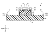
- FIG. 1 is a cross-sectional view showing the structure according to the first embodiment.
- FIG. 2 is a diagram showing the results of Raman spectroscopic measurement relating to the first embodiment.
- FIG. 3 is a cross-sectional view showing a structure according to the second embodiment.
- FIG. 4 is a diagram showing the results of Raman spectroscopic measurement relating to the second embodiment.
- FIG. 5 is a cross-sectional view showing a structure according to the third embodiment.
- FIG. 6 is a diagram showing the results of Raman spectroscopic measurement relating to the third embodiment.
- FIG. 7 is a top view showing a quantum bit according to the fourth embodiment.
- FIG. 8 is a cross-sectional view (Part 1) showing a quantum bit according to the fourth embodiment.
- FIG. 9 is a cross-sectional view (Part 2) showing the quantum bit according to the fourth embodiment.
- FIG. 10 is a perspective view showing a higher-order topological insulator layer.
- FIG. 11 is a top view (No. 1) showing the method of manufacturing the quantum bit according to the fourth embodiment.
- FIG. 12 is a top view (No. 2) showing the method of manufacturing the quantum bit according to the fourth embodiment.
- FIG. 13 is a top view (No. 3) showing the method of manufacturing the quantum bit according to the fourth embodiment.
- FIG. 14 is a top view (No. 4) showing the method of manufacturing the quantum bit according to the fourth embodiment.
- FIG. 15 is a top view (No. 5) showing the method of manufacturing the quantum bit according to the fourth embodiment.
- FIG. 16 is a top view (No.
- FIG. 17 is a cross-sectional view (part 1) showing the method of manufacturing the quantum bit according to the fourth embodiment.
- FIG. 18 is a cross-sectional view (part 2) showing the method of manufacturing the quantum bit according to the fourth embodiment.
- FIG. 19 is a cross-sectional view (No. 3) showing the method of manufacturing the quantum bit according to the fourth embodiment.
- FIG. 20 is a cross-sectional view (No. 4) showing the method of manufacturing the quantum bit according to the fourth embodiment.
- FIG. 21 is a cross-sectional view (No. 5) showing the method of manufacturing the quantum bit according to the fourth embodiment.
- FIG. 22 is a cross-sectional view (No. 6) showing the method of manufacturing the quantum bit according to the fourth embodiment.
- FIG. 23 is a diagram showing a quantum arithmetic device according to the fifth embodiment.
- the X1-X2 direction, the Y1-Y2 direction, and the Z1-Z2 direction are mutually orthogonal directions.
- a plane including the X1-X2 direction and the Y1-Y2 direction is referred to as the XY plane
- a plane including the Y1-Y2 direction and the Z1-Z2 direction is referred to as the YZ plane
- a plane including the Z1-Z2 direction and the X1-X2 direction. is described as the ZX plane.
- the Z1-Z2 direction is the vertical direction
- the Z1 side is the upper side
- the Z2 side is the lower side.
- the term “planar view” refers to viewing the object from the Z1 side
- the term “planar shape” refers to the shape of the object viewed from the Z1 side.
- FIG. 1 is a cross-sectional view showing the structure according to the first embodiment.
- the structure 100 has a substrate 110, a first layer 120, and a second layer .
- a first layer 120 is formed over the substrate 110 .
- a second layer 130 is formed over the first layer 120 .
- the substrate 110 is, for example, a single crystal substrate whose surface has a Miller index of (100).
- the material of the substrate 110 is MgO, for example.
- the substrate 110 in the first embodiment is an example of a base material.
- the first layer 120 is a Te layer that does not contain W.
- the thickness of the first layer 120 is, for example, 1 nm to 20 nm.
- the second layer 130 is, for example, multi-layer WTe2 .
- multilayer WTe 2 has 5 to 100 layers, preferably 10 to 50 layers of WTe 2 which is a two-dimensional material.
- a single layer of WTe 2 has a thickness of 0.7 nm, so if the second layer 130 contains 70 layers of WTe 2 , the thickness of the second layer 130 is about 50 nm.
- the substrate 110 is prepared, and the substrate 110 is annealed at about 1200° C. for 3 to 4 hours in an oxygen atmosphere of atmospheric pressure.
- the substrate 110 is immersed in methanol for 20 to 30 minutes and rinsed with ultrapure water. These treatments can improve the flatness of the surface of the substrate 110 .
- a first layer 120 is formed on the substrate 110 and a second layer 130 is formed on the first layer 120 .
- the first layer 120 and the second layer 130 can be epitaxially grown in situ in the same vacuum chamber, for example by pulse laser deposition (PLD).
- PLD pulse laser deposition
- the basic degree of vacuum when forming the first layer 120 and the second layer 130 is, for example, 5 ⁇ 10 ⁇ 6 Pa or less.
- the first layer 120 and the second layer 130 may be formed by a sputtering method, or the first layer 120 may be formed by a vapor deposition method and the second layer 130 may be formed by a co-evaporation method.
- the first layer 120 and the second layer 130 can be formed by physical vapor deposition in a vacuum-integrated process.
- a Te pure metal target can be used as the target.
- the temperature of the substrate 110 is maintained at about 200° C.
- the laser energy density is 1.0 J/cm 2
- the irradiation frequency is 1 Hz
- the distance between the substrate 110 and the target is about 5 cm
- the deposition rate is 1.0 nm/min.
- a WTe2 sintered body target can be used as the target.
- the temperature of the substrate 110 is maintained at 325° C.
- the laser energy density is 1.0 J/cm 2
- the irradiation frequency is 10 Hz
- the distance between the substrate 110 and the target is approximately 5 cm
- the deposition rate is 1.0 nm/min.
- the second layer 130 (multilayer WTe 2 ) is c-axis oriented on the first layer 120 and the crystal structure of the second layer 130 exhibits a Td structure.
- the structure 100 according to the first embodiment can be manufactured.
- first layer 120 is formed between substrate 110 and second layer 130 .
- the first layer 120 acts as a seed layer in forming the second layer 130, although the lattice mismatch between MgO with (100) surface Miller index and WTe2 is 33%. Therefore, good crystallinity can be obtained in the second layer 130 .
- FIG. 2 is a diagram showing the results of Raman spectroscopic measurement relating to the first embodiment.
- the material of the substrate 110 may be mica, sapphire, SiC, or the like.
- FIG. 3 is a cross-sectional view showing a structure according to the second embodiment.
- a structure 200 according to the second embodiment has a substrate 210, a first layer 120, and a second layer .
- a first layer 120 is formed over a substrate 210 .
- a second layer 130 is formed over the first layer 120 .
- the substrate 210 has a Si substrate 211 and a SiO 2 film 212 formed on the Si substrate 211 .
- the SiO 2 film 212 is formed by thermal oxidation of the Si substrate 211, for example. That is, the substrate 210 is a Si substrate with a thermal oxide film.
- a first layer 120 is provided on the SiO 2 film 212 .
- the substrate 210 in the second embodiment is an example of a base material.
- the substrate 210 is prepared, and the substrate 210 is annealed at about 800° C. for 15 minutes in an oxygen atmosphere of atmospheric pressure. Annealing can remove organic deposits on the surface of the SiO 2 film 212 .
- a first layer 120 is formed on the substrate 210 and a second layer 130 is formed on the first layer 120. Then, as shown in FIG.
- the first layer 120 and the second layer 130 can be formed by a method similar to that of the first embodiment.
- the structure 200 according to the second embodiment can be manufactured.
- first layer 120 is formed between substrate 210 and second layer 130 .
- the SiO 2 film 212 present on the surface of the substrate 210 is amorphous, the first layer 120 functions as a seed layer when forming the second layer 130 . Therefore, good crystallinity can be obtained in the second layer 130 .
- FIG. 4 is a diagram showing the results of Raman spectroscopic measurement relating to the second embodiment.
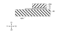
- FIG. 5 is a cross-sectional view showing a structure according to the third embodiment.
- a structure 300 according to the third embodiment has a substrate 110 , an s-wave superconductor layer 340 , a first layer 120 and a second layer 130 .
- An s-wave superconductor layer 340 is formed over the substrate 110 .
- a first layer 120 is formed over an s-wave superconductor layer 340 .
- a second layer 130 is formed over the first layer 120 .
- the s-wave superconductor layer 340 is, for example, a Nb layer with a surface Miller index of (110).
- the thickness of the s-wave superconductor layer 340 is, for example, about 100 nm to 200 nm.
- the laminate 310 of the substrate 110 and the s-wave superconductor layer 340 is an example of the base material.
- the substrate 110 is prepared, and annealing and rinsing are performed in the same manner as in the first embodiment.
- an s-wave superconductor layer 340 is formed on the substrate 110 , a first layer 120 is formed on the s-wave superconductor layer 340 , and a second layer 130 is formed on the first layer 120 .
- the s-wave superconductor layer 340, the first layer 120 and the second layer 130 can be epitaxially grown in situ in the same vacuum chamber, for example by the PLD method.
- the basic degree of vacuum when forming the s-wave superconductor layer 340, the first layer 120 and the second layer 130 is, for example, 5 ⁇ 10 ⁇ 6 Pa or less.
- the method of forming the s-wave superconductor layer 340, the first layer 120 and the second layer 130 is not limited to the PLD method.
- the s-wave superconductor layer 340, the first layer 120 and the second layer 130 may be formed by a sputtering method, the s-wave superconductor layer 340 and the first layer 120 are formed by a vapor deposition method, and the second layer 130 is formed by a vapor deposition method.
- Layer 130 may be formed by co-evaporation.
- a Nb pure metal target can be used as the target.
- the temperature of the substrate 110 is maintained at about 400° C.
- the laser energy density is 2.0 J/cm 2
- the irradiation frequency is 10 Hz
- the distance between the substrate 110 and the target is The distance between them is about 5 cm
- the deposition rate is 1.0 nm/min.
- the Nb layer is epitaxially grown while being oriented in the [110] direction on the substrate 110 kept at about 400.degree.
- the first layer 120 is formed on the s-wave superconductor layer 340 and the second layer 130 is formed on the first layer 120 .
- the first layer 120 and the second layer 130 can be formed by a method similar to that of the first embodiment.
- the s-wave superconductor layer 340, first layer 120 and second layer 130 can be formed by physical vapor deposition in a vacuum integrated process.
- the structure 300 according to the third embodiment can be manufactured.
- first layer 120 is formed between s-wave superconductor layer 340 and second layer 130 .
- the first layer 120 acts as a seed layer in forming the second layer 130, although the lattice mismatch between Nb with a surface Miller index of (110) and WTe2 is 25%. Therefore, good crystallinity can be obtained in the second layer 130 .
- the thickness of the s-wave superconductor layer 340 was 150 nm
- the thickness of the first layer 120 was 5 nm
- the thickness of the second layer 130 was 20 nm.
- FIG. 6 is a diagram showing the results of Raman spectroscopic measurement relating to the third embodiment.
- the material of the layered transition metal ditelluride layer contained in the second layer is not limited to WTe2 .
- the transition metal ditelluride layer may contain Mo, Nb, W, Ta, Ti, Zr, Fe, Pd, Ir or Pt or any combination thereof as the transition metal.
- the layered transition metal ditelluride layer contained in the second layer may be a single layer.
- the thickness of the first layer is preferably 1 nm to 20 nm. If the thickness of the first layer is less than 1 nm, it may be difficult to obtain excellent crystallinity in the second layer. Moreover, if the thickness of the first layer exceeds 20 nm, the electrical properties of the first layer may change. Furthermore, when the first layer is provided between the s-wave superconductor layer and the second layer, as in the third embodiment, if the thickness of the first layer is excessive, the superconducting proximity effect may decrease.
- the thickness of the first layer is more preferably 2 nm to 15 nm, still more preferably 3 nm to 10 nm.
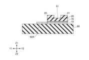
- FIG. 7 is a top view showing a quantum bit according to the fourth embodiment.
- 8 and 9 are cross-sectional views showing a quantum bit according to the fourth embodiment.
- FIG. 8 corresponds to a cross-sectional view taken along line VIII-VIII in FIG.
- FIG. 9 corresponds to a cross-sectional view taken along line IX-IX in FIG.
- the qubit 1 includes a substrate 90, an s-wave superconductor layer 10, a Te layer 70, a high-order topological insulator layer 20, a first ferromagnetic insulator layer 31, a second It has a ferromagnetic insulator layer 32 and a third ferromagnetic insulator layer 33 .
- the quantum bit 1 further includes a first gate electrode 41, a second gate electrode 42, a third gate electrode 43, a first superconducting quantum interference device (SQUID) 61, a second SQUID 62, and a third SQUID 63 .
- SQUID superconducting quantum interference device
- the substrate 90 is, for example, a single crystal substrate whose surface has a Miller index of (100).
- Materials for substrate 90 include MgO, mica, sapphire, and SiC.
- the substrate 90 may be a Si substrate with a thermal oxide film.
- the s-wave superconductor layer 10 is provided on part of the surface of the substrate 90 .
- the s-wave superconductor layer 10 is, for example, a Nb layer with a surface Miller index of (110).
- the thickness of the s-wave superconductor layer 10 is, for example, about 100 nm to 200 nm.
- the planar shape of the s-wave superconductor layer 10 is a rectangle having two sides parallel to the X1-X2 direction and two sides parallel to the Y1-Y2 direction.
- the Te layer 70 is provided on the s-wave superconductor layer 10 .
- the thickness of the Te layer 70 is preferably 1 nm to 20 nm, more preferably 2 nm to 15 nm, even more preferably 3 nm to 10 nm.
- the thickness of the Te layer 70 is, for example, 5 nm.
- Higher-order topological insulator layer 20 is provided on Te layer 70 .
- the higher-order topological insulator layer 20 is, for example, multi-layer WTe2 .
- multilayer WTe 2 has 5 to 100 layers, preferably 10 to 50 layers of WTe 2 which is a two-dimensional material.
- the thickness of the high-order topological insulator layer 20 is, for example, 20 nm.
- FIG. 10 is a perspective view showing the high-order topological insulator layer 20.
- the shape of the high-order topological insulator layer 20 is a substantially rectangular parallelepiped.
- the a-axis direction of the high-order topological insulator layer 20 is parallel to the Y1-Y2 direction, the b-axis direction is parallel to the X1-X2 direction, and the c-axis direction is parallel to the Z1-Z2 direction.
- the Miller index of the top surface of the high-order topological insulator layer 20 is (001), the Miller index of the side surface on the Y2 side is (100), and the Miller index of the side surface on the X2 side is (010).
- a T-shaped groove 50 is formed in the surface of the high-order topological insulator layer 20 in plan view.
- the groove 50 has a first groove 51 , a second groove 52 and a third groove 53 .
- the width of the first groove 51, the second groove 52 and the third groove 53 is 20 nm, and the depth is 10 nm.
- the first groove 51 and the third groove 53 extend parallel to the X1-X2 direction, and the second groove 52 extends parallel to the Y1-Y2 direction.
- the first groove 51 is provided near the center of the high-order topological insulator layer 20 in the Y1-Y2 direction and extends from the end of the high-order topological insulator layer 20 on the X2 side to the center in the X1-X2 direction.
- the third groove 53 is provided near the center of the high-order topological insulator layer 20 in the Y1-Y2 direction, and extends from the end of the high-order topological insulator layer 20 on the X1 side to the center in the X1-X2 direction. Therefore, the first groove 51 and the third groove 53 are formed in a straight line.
- the second groove 52 is provided near the center of the high-order topological insulator layer 20 in the X1-X2 direction and extends from the Y1-side end of the high-order topological insulator layer 20 to the center in the Y1-Y2 direction. Therefore, the second groove 52 is perpendicular to the first groove 51 and the third groove 53 .
- the high-order topological insulator layer 20 has the first region 21 on the Y2 side of the first groove 51 and the third groove 53 .
- the high-order topological insulator layer 20 has a second region 22 on the Y1 side of the first groove 51 and on the X2 side of the second groove 52 .
- the high-order topological insulator layer 20 has a third region 23 on the Y1 side of the third groove 53 and on the X1 side of the second groove 52 .
- Each of the first region 21, the second region 22 and the third region 23 has a hinge helical channel on one of two intersection lines of a plane perpendicular to the a-axis direction and a plane perpendicular to the c-axis direction.
- the hinge-helical channel is parallel to the b-axis.
- the first region 21 includes the first hinge helical channel 11 at the line of intersection (ridge line) between the top surface and the side surface on the Y1 side.
- the second region 22 has the second hinge helical channel 12 at the line of intersection between the side surface on the Y2 side and the bottom surface of the first groove 51 .
- the third region 23 has the third hinge helical channel 13 at the line of intersection between the side surface on the Y2 side and the bottom surface of the third groove 53 .
- the first hinge helical channel 11 is located at the line of intersection between the Y1 side surface of the first region 21 and the bottom surface of the groove 50
- the second hinge helical channel 12 is located between the upper surface of the second region 22 and the Y2 side surface. It may be on the line of intersection
- the third hinge-helical channel 13 may be on the line of intersection between the upper surface of the third region 23 and the side surface on the Y2 side.
- the first ferromagnetic insulator layer 31 is provided over part of the first region 21 , the second region 22 and the groove 50 and covers part of the first hinge helical channel 11 and the second hinge helical channel 12 . cover.
- a second ferromagnetic insulator layer 32 is provided over portions of the second region 22 , the third region 23 and the grooves 50 and partially overlies the second hinge helical channel 12 and the third hinge helical channel 13 . cover.
- a third ferromagnetic insulator layer 33 is provided over part of the third region 23 , the first region 21 and the groove 50 and covers part of the third hinge helical channel 13 and the first hinge helical channel 11 . cover.
- Examples of materials for the first ferromagnetic insulator layer 31, the second ferromagnetic insulator layer 32, and the third ferromagnetic insulator layer 33 include Cr2Ga2Te6 .
- the materials of the first ferromagnetic insulator layer 31, the second ferromagnetic insulator layer 32 and the third ferromagnetic insulator layer 33 may be other diluted magnetic semiconductors.
- the thicknesses of the first ferromagnetic insulator layer 31, the second ferromagnetic insulator layer 32, and the third ferromagnetic insulator layer 33 are, for example, about 30 nm.
- the second ferromagnetic insulator layer 32 is separated from the first ferromagnetic insulator layer 31 to the X1 side on the second hinge-helical channel 12 in the X1-X2 direction.
- the third ferromagnetic insulator layer 33 is separated from the second ferromagnetic insulator layer 32 to the X1 side on the third hinge-helical channel 13 in the X1-X2 direction.
- the third ferromagnetic insulator layer 33 is separated from the first ferromagnetic insulator layer 31 to the X1 side on the first hinge-helical channel 11 in the X1-X2 direction.
- the first gate electrode 41 is provided on the first ferromagnetic insulator layer 31 .
- a second gate electrode 42 is provided on the second ferromagnetic insulator layer 32 .
- a third gate electrode 43 is provided on the third ferromagnetic insulator layer 33 .
- Materials for the first gate electrode 41, the second gate electrode 42, and the third gate electrode 43 include Au.
- the thicknesses of the first gate electrode 41, the second gate electrode 42, and the third gate electrode 43 are, for example, about 100 nm.
- the first SQUID 61 has a lower superconductor layer 61A, a lower superconductor layer 61B, a tunnel barrier layer 61C, and an upper superconductor layer 61D.
- the lower superconductor layer 61A and the lower superconductor layer 61B protrude from the side surface of the s-wave superconductor layer 10 on the X2 side to the X2 side.
- the lower superconductor layer 61A is on the Y2 side of the lower superconductor layer 61B.
- the lower superconductor layer 61A protrudes from the first region 21 toward the X2 side
- the lower superconductor layer 61B protrudes from the second region 22 toward the X2 side.
- the lower superconductor layer 61 A and the lower superconductor layer 61 B are formed integrally with the s-wave superconductor layer 10 from the same material as the s-wave superconductor layer 10 .
- the lower superconductor layer 61 A and the lower superconductor layer 61 B are connected to the s-wave superconductor layer 10 .
- the lower superconductor layer 61A and the lower superconductor layer 61B are, for example, Nb layers with a thickness of about 100 nm to 200 nm.
- the tunnel barrier layer 61C and the upper superconductor layer 61D have a U-shaped planar shape.
- a material for the tunnel barrier layer 61C is NbOx
- a material for the upper superconductor layer 61D is Nb.
- the thickness of the tunnel barrier layer 61C is, for example, about 1 nm to 5 nm
- the thickness of the upper superconductor layer 61D is, for example, about 100 nm to 200 nm.
- One end of the tunnel barrier layer 61C contacts the lower superconductor layer 61A and the other end contacts the lower superconductor layer 61B.
- An upper superconductor layer 61D is provided on the tunnel barrier layer 61C.
- a tunnel barrier layer 61C is sandwiched between the lower superconductor layer 61A and the upper superconductor layer 61D and between the lower superconductor layer 61B and the upper superconductor layer 61D.
- the first SQUID 61 is composed of such a Josephson junction.
- the first SQUID 61 detects changes in magnetic flux between the first hinge helical channel 11 and the second hinge helical channel 12 .
- the second SQUID 62 has a lower superconductor layer 62A, a lower superconductor layer 62B, a tunnel barrier layer 62C, and an upper superconductor layer 62D.
- the lower superconductor layer 62A and the lower superconductor layer 62B protrude from the side surface of the s-wave superconductor layer 10 on the Y1 side to the Y1 side.
- the lower superconductor layer 62A is on the X2 side of the lower superconductor layer 62B.
- the lower superconductor layer 62A protrudes from the second region 22 toward the Y1 side
- the lower superconductor layer 62B protrudes from the third region 23 toward the Y1 side.
- the lower superconductor layer 62A and the lower superconductor layer 62B are formed integrally with the s-wave superconductor layer 10 from the same material as the s-wave superconductor layer 10.
- Lower superconductor layer 62 A and lower superconductor layer 62 B are connected to s-wave superconductor layer 10 .
- the lower superconductor layer 62A and the lower superconductor layer 62B are, for example, Nb layers with a thickness of about 100 nm to 200 nm.
- the tunnel barrier layer 62C and the upper superconductor layer 62D have a U-shaped planar shape.
- a material for the tunnel barrier layer 62C is NbOx
- a material for the upper superconductor layer 62D is Nb.
- the thickness of the tunnel barrier layer 62C is, for example, about 1 nm to 5 nm
- the thickness of the upper superconductor layer 62D is, for example, about 100 nm to 200 nm.
- One end of the tunnel barrier layer 62C contacts the lower superconductor layer 62A and the other end contacts the lower superconductor layer 62B.
- An upper superconductor layer 62D is provided over the tunnel barrier layer 62C.
- a tunnel barrier layer 62C is sandwiched between the lower superconductor layer 62A and the upper superconductor layer 62D and between the lower superconductor layer 62B and the upper superconductor layer 62D.
- the second SQUID 62 is composed of such a Josephson junction.
- the second SQUID 62 detects changes in magnetic flux between the second hinge-helical channel 12 and the third hinge-helical channel 13 .
- the third SQUID 63 has a lower superconductor layer 63A, a lower superconductor layer 63B, a tunnel barrier layer 63C, and an upper superconductor layer 63D.
- the lower superconductor layer 63A and the lower superconductor layer 63B protrude from the side surface of the s-wave superconductor layer 10 on the X1 side to the X1 side.
- the lower superconductor layer 63A is on the Y1 side of the lower superconductor layer 63B.
- the lower superconductor layer 63A protrudes from the third region 23 toward the X1 side
- the lower superconductor layer 63B protrudes from the first region 21 toward the X1 side.
- the lower superconductor layer 63 A and the lower superconductor layer 63 B are formed integrally with the s-wave superconductor layer 10 from the same material as the s-wave superconductor layer 10 .
- the lower superconductor layer 63 A and the lower superconductor layer 63 B are connected to the s-wave superconductor layer 10 .
- the lower superconductor layer 63A and the lower superconductor layer 63B are, for example, Nb layers with a thickness of about 100 nm to 200 nm.
- the tunnel barrier layer 63C and the upper superconductor layer 63D have a U-shaped planar shape.
- a material for the tunnel barrier layer 63C is NbOx
- a material for the upper superconductor layer 63D is Nb.
- the thickness of the tunnel barrier layer 63C is, for example, about 1 nm to 5 nm
- the thickness of the upper superconductor layer 63D is, for example, about 100 nm to 200 nm.
- One end of the tunnel barrier layer 63C contacts the lower superconductor layer 63A and the other end contacts the lower superconductor layer 63B.
- An upper superconductor layer 63D is provided on the tunnel barrier layer 63C.
- a tunnel barrier layer 63C is sandwiched between the lower superconductor layer 63A and the upper superconductor layer 63D and between the lower superconductor layer 63B and the upper superconductor layer 63D.
- the third SQUID 63 is composed of such a Josephson junction.
- the third SQUID 63 detects changes in magnetic flux between the third hinge helical channel 13 and the first hinge helical channel 11 .
- the Majorana particle ⁇ 1 is stably expressed near the first gate electrode 41 of the first hinge-helical channel 11
- the Majorana particle ⁇ 4 is stably expressed near the third gate electrode 43 of the first hinge-helical channel 11.
- the Majorana particle ⁇ 2 is stably expressed between the first gate electrode 41 and the second gate electrode 42 of the second hinge-helical channel 12
- the Majorana particle ⁇ 3 is stably expressed in the third hinge-helical channel 13. It is stably developed between the second gate electrode 42 and the third gate electrode 43 .
- Exchange of the Majorana particles ⁇ 1 to ⁇ 4 is carried out by a change in electrostatic potential caused by application of gate voltages to the first gate electrode 41, the second gate electrode 42, and the third gate electrode 43.
- the first gate electrode 41 when the Majorana particles ⁇ 1 and ⁇ 2 are exchanged, an electric field is applied from the first gate electrode 41, and the first SQUID 61 detects a minute change in magnetic flux as a minute change in voltage signal when the Majorana particles ⁇ 1 and ⁇ 2 are exchanged. detected.
- the second SQUID 62 detects minute changes in the magnetic flux during the exchange of the Majorana particles ⁇ 2 and ⁇ 3 as minute voltage signal changes.
- a monolayer film of WTe2 which is a layered material of transition metal dichalcogenide, is easily oxidized, and its properties change when exposed to the atmosphere. It is possible to suppress oxidation by sandwiching a single layer of WTe 2 between hexagonal boron nitride (h-BN), graphene, or other chemically stable substances. It complicates the process. It is also difficult to adjust the size of the WTe2 monolayer film.
- the high-order topological insulator layer 20 such as multilayer WTe 2 is used, a structure for suppressing oxidation is not required.
- adjusting the size of the high-order topological insulator layer 20 is easier than adjusting the size of a single layer film of WTe 2 .
- 11 to 16 are top views showing the manufacturing method of the quantum bit 1 according to the fourth embodiment.
- 17 to 22 are cross-sectional views showing the manufacturing method of the quantum bit 1 according to the fourth embodiment.
- FIGS. 11 and 17 corresponds to a cross-sectional view taken along line XVII-XVII in FIG.
- the s-wave superconductor layer 19 is formed on the substrate 90 , the Te layer 79 is formed on the s-wave superconductor layer 19 , and the high-order topological insulator layer 29 is formed on the Te layer 79 .
- an Nb layer is formed as the s-wave superconductor layer 19 and a multi-layered WTe 2 is formed as the high-order topological insulator layer 29 .
- the s-wave superconductor layer 19, the Te layer 79, and the high-order topological insulator layer 29 can be epitaxially grown in situ in the same vacuum chamber by, for example, the PLD method.
- the basic degree of vacuum at the time of forming the s-wave superconductor layer 19, Te layer 79, and high-order topological insulator layer 29 is, for example, 5 ⁇ 10 ⁇ 6 Pa or less.
- the method of forming the s-wave superconductor layer 19, the Te layer 79, and the high-order topological insulator layer 29 is not limited to the PLD method.
- the s-wave superconductor layer 19, the Te layer 79, and the high-order topological insulator layer 29 may be formed by a sputtering method, and the s-wave superconductor layer 19 and the Te layer 79 may be formed by a vapor deposition method.
- the next topological insulator layer 29 may be formed by co-evaporation.
- the s-wave superconductor layer 19, Te layer 79 and higher topological insulator layer 29 can be formed by physical vapor deposition in a vacuum integrated process.
- a Nb pure metal target can be used as the target.
- the temperature of the substrate 90 is maintained at about 400° C.
- the laser energy density is 2.0 J/cm 2 to 5.0 J/cm 2
- the irradiation frequency is 10 Hz.
- the distance between the substrate 90 and the target is about 5 cm
- the deposition rate is 0.5 nm/min to 1.0 nm/min.
- the Nb layer is epitaxially grown while being oriented in the [110] direction on the substrate 90 kept at about 400.degree.
- a Te pure metal target can be used as a target.
- the temperature of the substrate 90 is maintained at about 200° C.
- the laser energy density is 1.0 J/cm 2 to 2.0 J/cm 2
- the irradiation frequency is 1 Hz
- the substrate 110 and The distance from the target is about 5 cm
- the deposition rate is 0.5 nm/min to 1.5 nm/min.
- a WTe2 sintered body target can be used as the target.
- the temperature of the substrate 90 is maintained at about 325° C.
- the laser energy density is 1.0 J/cm 2 to 2.0 J/cm 2
- the irradiation frequency is 10 Hz
- the distance between the substrate 90 and the target is about 5 cm
- the deposition rate is 0.5 nm/min to 1.5 nm/min.
- the higher-order topological insulator layer 29 (multilayer WTe 2 ) is oriented in the c-axis direction on the s-wave superconductor layer 19 (Nb layer), and the crystal structure of the higher-order topological insulator layer 29 exhibits a Td structure.
- FIG. 18 corresponds to a cross-sectional view taken along line XVIII-XVIII in FIG.
- the high-order topological insulator layer 29 is spin-coated with a first electron beam resist.
- a first mask pattern is formed from the first electron beam resist.
- the first mask pattern is the s-wave superconductor layer 10, the lower superconductor layer 61A, the lower superconductor layer 61B, the lower superconductor layer 62A, and the lower superconductor layer 62B of the s-wave superconductor layer 19.
- the portion where the lower superconductor layer 63A and the lower superconductor layer 63B are to be formed are covered from above the high-order topological insulator layer 29, and other portions are exposed.
- the first electron beam resist for example, a resist obtained by diluting ZEP 520A (manufactured by Nippon Zeon Co., Ltd.) with ZEP-A (manufactured by Nippon Zeon Co., Ltd.) at a ratio of 1:1 can be used.
- the s-wave superconductor layer 19, Te layer 79 and high-order topological insulator layer 29 are processed by Ar ion milling.
- Ar ion milling for example, the beam acceleration voltage is 280 V and the beam current is 150 mA.
- FIG. 19 corresponds to a cross-sectional view taken along line XIX-XIX in FIG.
- a second electron beam resist is spin-coated on the high-order topological insulator layer 29 and the substrate 90 .
- a second mask pattern is formed from a second electron beam resist by electron beam lithography.
- the second mask pattern covers the portion of the higher-order topological insulator layer 29 on the s-wave superconductor layer 10, the lower superconductor layer 61A, the lower superconductor layer 61B, the lower superconductor layer 62A, the lower superconductor layer 62A, the lower superconductor layer The conductor layer 62B, the lower superconductor layer 63A and the upper portions of the lower superconductor layer 63B are exposed.
- the second electron beam resist for example, a resist obtained by diluting ZEP 520A (manufactured by Nippon Zeon Co., Ltd.) with ZEP-A (manufactured by Nippon Zeon Co., Ltd.) at a ratio of 1:1 can be used.
- the high-order topological insulator layer 29 and the Te layer 79 are processed by Ar ion milling.
- the higher-order topological insulator layer 29A and the Te layer 70 are formed, and the lower superconductor layer 61A, the lower superconductor layer 61B, the lower superconductor layer 62A, the lower superconductor layer 62B, the lower superconductor Layer 63 A and lower superconductor layer 63 B are exposed from higher topological insulator layer 29 A and Te layer 70 .
- the beam acceleration voltage is 280 V and the beam current is 150 mA.
- FIG. 20 corresponds to a cross-sectional view taken along line XX-XX in FIG.
- the high-order topological insulator layer 29A When processing the high-order topological insulator layer 29A, first, the high-order topological insulator layer 29A, the substrate 90, the lower superconductor layer 61A, the lower superconductor layer 61B, the lower superconductor layer 62A, the lower superconductor layer A third electron beam resist is spin-coated on the conductor layer 62B, the lower superconductor layer 63A and the lower superconductor layer 63B. Next, by electron beam lithography, a third mask pattern is formed from a third electron beam resist. The third mask pattern exposes the portion of the high-order topological insulator layer 29A where the trench 50 is to be formed and covers the other portion.
- the third electron beam resist for example, a resist obtained by diluting ZEP 520A (manufactured by Nippon Zeon Co., Ltd.) with ZEP-A (manufactured by Nippon Zeon Co., Ltd.) at a ratio of 1:1 can be used.
- the high-order topological insulator layer 29A is processed by Ar ion milling. As a result, a trench 50 comprising a first trench 51, a second trench 52 and a third trench 53 is formed, and a high-order topological insulator layer 20 comprising a first region 21, a second region 22 and a third region 23 is formed. is obtained.
- the first region 21 comprises the first hinge helical channel 11
- the second region 22 comprises the second hinge helical channel 12
- the third region 23 comprises the third hinge helical channel 13 (see Figure 10).
- the beam acceleration voltage is 280 V and the beam current is 150 mA.
- FIG. 21 corresponds to a cross-sectional view taken along line XXI-XXI in FIG.
- the first ferromagnetic insulator layer 31 When forming the first ferromagnetic insulator layer 31, the second ferromagnetic insulator layer 32, the third ferromagnetic insulator layer 33, the first gate electrode 41, the second gate electrode 42 and the third gate electrode 43, First, the higher-order topological insulator layer 20, the substrate 90, the lower superconductor layer 61A, the lower superconductor layer 61B, the lower superconductor layer 62A, the lower superconductor layer 62B, the lower superconductor layer 63A and the lower A fourth electron beam resist is spin-coated on the superconductor layer 63B. Next, a fourth mask pattern is formed from a fourth electron beam resist by electron beam lithography.
- the fourth mask pattern includes a first ferromagnetic insulator layer 31, a second ferromagnetic insulator layer 32, a third ferromagnetic insulator layer 33, a first gate electrode 41, a second gate electrode 42 and a third gate electrode 43. It exposes the part that is to form the , and covers the other part.
- the fourth electron beam resist for example, a resist obtained by diluting ZEP 520A (manufactured by Nippon Zeon Co., Ltd.) with ZEP-A (manufactured by Nippon Zeon Co., Ltd.) at a ratio of 1:1 can be used.
- a Cr 2 Ga 2 Te 6 layer and an Au layer are formed by the PLD method.
- the temperature of the substrate 90 is maintained at 200° C.
- the laser energy density is 1.0 J/cm 2 to 2.0 J/cm 2
- the irradiation frequency is is 1 Hz
- the distance between the substrate 90 and the target is about 5 cm
- the deposition rate is 1.0 nm/min to 2.0 nm/min.
- the temperature of the substrate 90 is kept at room temperature, the laser energy density is 1.0 J/cm 2 to 2.0 J/cm 2 , the irradiation frequency is 5 Hz, and the substrate 90 is The distance from the target is about 5 cm, and the deposition rate is 5.0 nm/min to 10.0 nm/min.
- the fourth mask pattern is removed together with the Cr 2 Ga 2 Te 6 layer and the Au layer deposited thereon. That is, liftoff is performed.
- a first ferromagnetic insulator layer 31 a second ferromagnetic insulator layer 32, a third ferromagnetic insulator layer 33, a first gate electrode 41, a second gate electrode 42 and a third gate electrode 43 are obtained.
- four Majorana particles ⁇ 1, ⁇ 2, ⁇ 3 and ⁇ 4 are expressed.
- FIG. 22 corresponds to a cross-sectional view taken along line XXII-XXII in FIG.
- the tunnel barrier layers 61C-63C and the upper superconductor layers 61D-63D When forming the tunnel barrier layers 61C-63C and the upper superconductor layers 61D-63D, first, the higher-order topological insulator layer 20, the substrate 90, the lower superconductor layer 61A, the lower superconductor layer 61B, the lower fifth electrons on superconductor layer 62A, lower superconductor layer 62B, lower superconductor layer 63A, lower superconductor layer 63B, first gate electrode 41, second gate electrode 42 and third gate electrode 43; Spin coat the line resist. Next, by electron beam lithography, a fifth mask pattern is formed from a fifth electron beam resist.
- the fifth mask pattern exposes portions where the tunnel barrier layers 61C-63C and upper superconductor layers 61D-63D are to be formed, and covers other portions.
- the fifth electron beam resist for example, a resist obtained by diluting ZEP 520A (manufactured by Nippon Zeon Co., Ltd.) with ZEP-A (manufactured by Nippon Zeon Co., Ltd.) at a ratio of 1:1 can be used.
- an NbOx layer and an Nb layer are formed by the PLD method.
- the temperature of the substrate 90 is maintained at room temperature, and the oxygen partial pressure in the vacuum chamber is adjusted to about 50 Pa to 55 Pa.
- the Nb layer can be formed under the same conditions as the s-wave superconductor layer 19 .
- the fifth mask pattern is removed together with the NbOx and Nb layers deposited thereon. That is, liftoff is performed. As a result, tunnel barrier layers 61C-63C and upper superconductor layers 61D-63D are obtained, and a first SQUID 61, a second SQUID 62 and a third SQUID 63 are formed.
- the quantum bit 1 according to the fourth embodiment can be manufactured.
- the material of the higher topological insulator layer 20 is not limited to multi-layer WTe2 .
- the higher topological insulator layer 20 may contain Mo, Nb, W, Ta, Ti, Zr, Fe, Pd, Ir or Pt or any combination thereof as transition metals.
- the material of the s-wave superconductor layer 10 is not limited to Nb, and may be Al or Pd, for example.
- the thickness of the Te layer 70 is preferably 1 nm to 20 nm, more preferably 2 nm to 15 nm, even more preferably 3 nm to 10 nm. If the Te layer 70 is excessively thick, the superconducting proximity effect of the s-wave superconductor layer may be degraded.
- the fifth embodiment relates to a quantum arithmetic device including the quantum bit 1 according to the fourth embodiment.
- FIG. 23 is a diagram showing a quantum arithmetic device according to the fifth embodiment.
- the quantum arithmetic device 2 has a quantum bit chip 81, a signal generator 82, a signal demodulator 83, and a cryogenic dilution refrigerator 84, as shown in FIG.
- a qubit chip 81 includes a plurality of qubits 1 according to the fourth embodiment.
- a qubit chip 81 is housed in a cryogenic dilution refrigerator 84 and cooled to a temperature of 10 mK or less.
- a signal generator 82 generates a microwave pulse signal, and the microwave pulse signal is input to the qubit chip 81 .
- the quantum bit chip 81 outputs a signal corresponding to the microwave pulse signal, and the signal demodulator 83 demodulates the signal output from the quantum bit chip 81 .
- the signal generator 82 and signal demodulator 83 are used, for example, at room temperature.
- the quantum arithmetic device 2 according to the fifth embodiment includes the quantum bit 1 according to the fourth embodiment, the Majorana particles can be stably expressed, and stable computation can be performed.
- Quantum bit 2 Quantum arithmetic device 10: s-wave superconductor layer 11: First hinge helical channel 12: Second hinge helical channel 13: Third hinge helical channel 20: Higher order topological insulator layer 21: First Region 22: Second region 23: Third region 31: First ferromagnetic insulator layer 32: Second ferromagnetic insulator layer 33: Third ferromagnetic insulator layer 41: First gate electrode 42: Second gate electrode 43: Third gate electrode 50: Groove 51: First groove 52: Second groove 53: Third groove 61: First SQUID 62: Second SQUID 63: Third SQUID 100, 200, 300: structure 110, 210: substrate 120: first layer 130: second layer 211: Si substrate 212: SiO 2 film 310: laminate 340: s-wave superconductor layer
Landscapes
- Engineering & Computer Science (AREA)
- Manufacturing & Machinery (AREA)
- Superconductor Devices And Manufacturing Methods Thereof (AREA)
Abstract
In the present invention, a structure (100) comprises a base (110), a first layer (120) provided on the base, and a second layer (130) provided on the first layer. The first layer is a Te layer, and the second layer has a transition metal ditelluride layer.
Description
本開示は、構造体、量子ビット、量子演算装置及び構造体の製造方法に関する。
The present disclosure relates to structures, quantum bits, quantum computing devices, and methods of manufacturing structures.
マヨラナ粒子を用いた量子演算装置についての研究が行われている。マヨラナ粒子を発生させる構造として、二次元トポロジカル絶縁体とs波超伝導体とを組み合わせた構造が提案されている。二次元トポロジカル絶縁体としては、遷移金属ダイテルライドの層状物質であるWTe2の単層膜が用いられている。また、多層WTe2からなる高次トポロジカル絶縁体層についての研究も行われている。
Quantum computing devices using Majorana particles are being researched. A structure combining a two-dimensional topological insulator and an s-wave superconductor has been proposed as a structure for generating Majorana particles. As a two-dimensional topological insulator, a single-layer film of WTe2 , which is a layered material of transition metal ditelluride, is used. Research has also been conducted on high-order topological insulator layers composed of multilayer WTe2 .
これまで理論に基づく提案はされているものの、結晶性が良好なWTe2等の遷移金属ダイテルライド層を安定して得ることは容易ではない。
Although proposals based on theory have been made so far, it is not easy to stably obtain a transition metal ditelluride layer such as WTe2 with good crystallinity.
本開示の目的は、遷移金属ダイテルライド層に良好な結晶性を得ることができる構造体、量子ビット、量子演算装置及び構造体の製造方法を提供することにある。
An object of the present disclosure is to provide a structure, a quantum bit, a quantum computing device, and a method of manufacturing the structure that can obtain good crystallinity in the transition metal ditelluride layer.
本開示の一形態によれば、基材と、前記基材上に設けられた第1層と、前記第1層上に設けられた第2層と、を有し、前記第1層は、Te層であり、前記第2層は、遷移金属ダイテルライド層を有する構造体が提供される。
According to one aspect of the present disclosure, it has a substrate, a first layer provided on the substrate, and a second layer provided on the first layer, the first layer comprising: A structure is provided having a Te layer and said second layer comprising a transition metal ditelluride layer.
本開示によれば、遷移金属ダイテルライド層に良好な結晶性を得ることができる。
According to the present disclosure, good crystallinity can be obtained in the transition metal ditelluride layer.
以下、本開示の実施形態について添付の図面を参照しながら具体的に説明する。なお、本明細書及び図面において、実質的に同一の機能構成を有する構成要素については、同一の符号を付することにより重複した説明を省くことがある。本開示においては、X1-X2方向、Y1-Y2方向、Z1-Z2方向を相互に直交する方向とする。X1-X2方向及びY1-Y2方向を含む面をXY面と記載し、Y1-Y2方向及びZ1-Z2方向を含む面をYZ面と記載し、Z1-Z2方向及びX1-X2方向を含む面をZX面と記載する。なお、便宜上、Z1-Z2方向を上下方向とし、Z1側を上側、Z2側を下側とする。また、平面視とは、Z1側から対象物を視ることをいい、平面形状とは、対象物をZ1側から視た形状のことをいう。
Hereinafter, embodiments of the present disclosure will be specifically described with reference to the attached drawings. In the present specification and drawings, constituent elements having substantially the same functional configuration may be denoted by the same reference numerals, thereby omitting redundant description. In the present disclosure, the X1-X2 direction, the Y1-Y2 direction, and the Z1-Z2 direction are mutually orthogonal directions. A plane including the X1-X2 direction and the Y1-Y2 direction is referred to as the XY plane, a plane including the Y1-Y2 direction and the Z1-Z2 direction is referred to as the YZ plane, and a plane including the Z1-Z2 direction and the X1-X2 direction. is described as the ZX plane. For convenience, the Z1-Z2 direction is the vertical direction, the Z1 side is the upper side, and the Z2 side is the lower side. Further, the term "planar view" refers to viewing the object from the Z1 side, and the term "planar shape" refers to the shape of the object viewed from the Z1 side.
(第1実施形態)
まず、第1実施形態について説明する。第1実施形態は構造体に関する。図1は、第1実施形態に係る構造体を示す断面図である。 (First embodiment)
First, the first embodiment will be explained. A first embodiment relates to a structure. FIG. 1 is a cross-sectional view showing the structure according to the first embodiment.
まず、第1実施形態について説明する。第1実施形態は構造体に関する。図1は、第1実施形態に係る構造体を示す断面図である。 (First embodiment)
First, the first embodiment will be explained. A first embodiment relates to a structure. FIG. 1 is a cross-sectional view showing the structure according to the first embodiment.
第1実施形態に係る構造体100は、基板110と、第1層120と、第2層130とを有する。第1層120は基板110の上に形成されている。第2層130は第1層120の上に形成されている。
The structure 100 according to the first embodiment has a substrate 110, a first layer 120, and a second layer . A first layer 120 is formed over the substrate 110 . A second layer 130 is formed over the first layer 120 .
基板110は、例えば表面のミラー指数が(100)の単結晶基板である。基板110の材料は、例えばMgOである。第1実施形態において基板110は基材の一例である。
The substrate 110 is, for example, a single crystal substrate whose surface has a Miller index of (100). The material of the substrate 110 is MgO, for example. The substrate 110 in the first embodiment is an example of a base material.
第1層120は、Wを含まないTe層である。第1層120の厚さは、例えば1nm~20nmである。
The first layer 120 is a Te layer that does not contain W. The thickness of the first layer 120 is, for example, 1 nm to 20 nm.
第2層130は、例えば多層WTe2である。例えば、多層WTe2は、2次元材料であるWTe2を5層~100層、好ましくは10層~50層有する。単層のWTe2の厚さが0.7nmであるため、第2層130が70層のWTe2を含む場合、第2層130の厚さは約50nmである。
The second layer 130 is, for example, multi-layer WTe2 . For example, multilayer WTe 2 has 5 to 100 layers, preferably 10 to 50 layers of WTe 2 which is a two-dimensional material. A single layer of WTe 2 has a thickness of 0.7 nm, so if the second layer 130 contains 70 layers of WTe 2 , the thickness of the second layer 130 is about 50 nm.
次に、第1実施形態に係る構造体100の製造方法について説明する。ここでは、基板110としてミラー指数が(100)のMgO単結晶基板を用い、第1層120としてTe層を形成し、第2層130として多層WTe2を形成することとして説明する。
Next, a method for manufacturing the structure 100 according to the first embodiment will be described. Here, it is assumed that an MgO single crystal substrate having a Miller index of (100) is used as the substrate 110, a Te layer is formed as the first layer 120, and a multilayer WTe2 is formed as the second layer .
まず、基板110を準備し、大気圧の酸素雰囲気下で、約1200℃で3時間~4時間の基板110のアニール処理を行う。次いで、基板110をメタノールに20分間~30分間浸漬し、超純水でリンス処理を行う。これらの処理により、基板110の表面の平坦性を向上することができる。
First, the substrate 110 is prepared, and the substrate 110 is annealed at about 1200° C. for 3 to 4 hours in an oxygen atmosphere of atmospheric pressure. Next, the substrate 110 is immersed in methanol for 20 to 30 minutes and rinsed with ultrapure water. These treatments can improve the flatness of the surface of the substrate 110 .
次いで、基板110上に第1層120を形成し、第1層120上に第2層130を形成する。第1層120及び第2層130は、例えばパルスレーザー堆積(pulse laser deposition:PLD)法により、同一の真空槽内で、in situでエピタキシャル成長させることができる。第1層120及び第2層130の形成時の基本真空度は、例えば5×10⁻⁶Pa以下とする。PLD法により、第1層120及び第2層130を形成する際には、レーザ光源としてKrFエキシマレーザ(λ=248nm)光源を用いることができる。なお、第1層120及び第2層130の形成方法はPLD法に限定されない。例えば、第1層120及び第2層130をスパッタ法により形成してもよく、第1層120を蒸着法により形成し、第2層130を共蒸着法により形成してもよい。このように、第1層120及び第2層130は、真空一貫プロセスで物理蒸着法により形成することができる。
Next, a first layer 120 is formed on the substrate 110 and a second layer 130 is formed on the first layer 120 . The first layer 120 and the second layer 130 can be epitaxially grown in situ in the same vacuum chamber, for example by pulse laser deposition (PLD). The basic degree of vacuum when forming the first layer 120 and the second layer 130 is, for example, 5×10 −6 Pa or less. When forming the first layer 120 and the second layer 130 by the PLD method, a KrF excimer laser (λ=248 nm) light source can be used as the laser light source. Note that the method for forming the first layer 120 and the second layer 130 is not limited to the PLD method. For example, the first layer 120 and the second layer 130 may be formed by a sputtering method, or the first layer 120 may be formed by a vapor deposition method and the second layer 130 may be formed by a co-evaporation method. Thus, the first layer 120 and the second layer 130 can be formed by physical vapor deposition in a vacuum-integrated process.
第1層120の形成の際には、例えば、ターゲットにはTe純金属ターゲットを用いることができる。第1層120を形成する際には、例えば、基板110の温度を約200℃に保持し、レーザエネルギー密度を1.0J/cm2、照射周波数を1Hz、基板110とターゲットとの間の距離を約5cm、成膜レートを1.0nm/分とする。
When forming the first layer 120, for example, a Te pure metal target can be used as the target. When forming the first layer 120, for example, the temperature of the substrate 110 is maintained at about 200° C., the laser energy density is 1.0 J/cm 2 , the irradiation frequency is 1 Hz, and the distance between the substrate 110 and the target is is about 5 cm, and the deposition rate is 1.0 nm/min.
第2層130として多層WTe2をPLD法により形成する場合、例えば、ターゲットにはWTe2焼結体ターゲットを用いることができる。第2層130を形成する際には、例えば、基板110の温度を325℃に保持し、レーザエネルギー密度1.0J/cm2、照射周波数を10Hz、基板110とターゲットとの間の距離を約5cm、成膜レートを1.0nm/分とする。第2層130(多層WTe2)は第1層120上でc軸方向に配向し、第2層130の結晶構造はTd構造を示す。
When forming a multilayer WTe2 as the second layer 130 by the PLD method, for example, a WTe2 sintered body target can be used as the target. When forming the second layer 130, for example, the temperature of the substrate 110 is maintained at 325° C., the laser energy density is 1.0 J/cm 2 , the irradiation frequency is 10 Hz, and the distance between the substrate 110 and the target is approximately 5 cm, and the deposition rate is 1.0 nm/min. The second layer 130 (multilayer WTe 2 ) is c-axis oriented on the first layer 120 and the crystal structure of the second layer 130 exhibits a Td structure.
このようにして、第1実施形態に係る構造体100を製造することができる。
Thus, the structure 100 according to the first embodiment can be manufactured.
構造体100では、基板110と第2層130との間に第1層120が形成されている。表面のミラー指数が(100)のMgOとWTe2との間の格子不整合は33%であるが、第1層120が第2層130を形成する際のシード層として機能する。このため、第2層130に良好な結晶性を得ることができる。
In structure 100 , first layer 120 is formed between substrate 110 and second layer 130 . The first layer 120 acts as a seed layer in forming the second layer 130, although the lattice mismatch between MgO with (100) surface Miller index and WTe2 is 33%. Therefore, good crystallinity can be obtained in the second layer 130 .
なお、多層WTe2を成膜の後に、約300℃で30分間~1時間ポストアニールを行うことが好ましい。多層WTe2の結晶性が向上するためである。
It is preferable to perform post-annealing at about 300° C. for 30 minutes to 1 hour after depositing the multi-layered WTe 2 . This is because the crystallinity of the multilayer WTe 2 is improved.
次に、本発明者が行った第1実施形態に関するラマン分光測定の結果について説明する。この測定では、第1実施形態に倣って試料を作成し、この試料についてラマン分光測定を行った。なお、第1層120の厚さは10nmとし、第2層130の厚さは50nmとした。また、参考のために、第1層120を形成せずに、基板110の上に第2層130を形成した試料(第1参考例)と、基板110のみの試料(第2参考例)とを作成し、これら試料についてもラマン分光測定を行った。図2は、第1実施形態に関するラマン分光測定の結果を示す図である。
Next, the results of the Raman spectroscopic measurement regarding the first embodiment performed by the inventor will be described. In this measurement, a sample was prepared according to the first embodiment, and Raman spectroscopic measurement was performed on this sample. The thickness of the first layer 120 was set to 10 nm, and the thickness of the second layer 130 was set to 50 nm. For reference, a sample (first reference example) in which the second layer 130 is formed on the substrate 110 without forming the first layer 120 and a sample (second reference example) in which only the substrate 110 is formed are shown. were prepared, and Raman spectroscopy was performed on these samples as well. FIG. 2 is a diagram showing the results of Raman spectroscopic measurement relating to the first embodiment.
図2に示すように、第1実施形態の試料ではWTe2に由来する格子振動モード(A1
2、A1
5、A1
8、A1
9、A2
4)のシャープなピークが確認できるのに対し、第1参考例の試料ではA1
2モード及びA1
5モードのブロードなピークが見られるのみである。これらの結果から、第1層120が設けられることで、第2層130の結晶性が向上していることが確認できる。
As shown in FIG. 2, in the sample of the first embodiment , sharp peaks of lattice vibration modes ( A 12 , A 15 , A 18 , A 19 , A 24 ) derived from WTe 2 can be confirmed . On the other hand, in the sample of the first reference example, only broad peaks of A 1 2 mode and A 1 5 mode are observed. From these results, it can be confirmed that the crystallinity of the second layer 130 is improved by providing the first layer 120 .
なお、基板110の材料がマイカ、サファイア又はSiC等であってもよい。
Note that the material of the substrate 110 may be mica, sapphire, SiC, or the like.
(第2実施形態)
次に、第2実施形態について説明する。第2実施形態は、主として基板の構成の点で第1実施形態と相違する。図3は、第2実施形態に係る構造体を示す断面図である。 (Second embodiment)
Next, a second embodiment will be described. The second embodiment differs from the first embodiment mainly in the configuration of the substrate. FIG. 3 is a cross-sectional view showing a structure according to the second embodiment.
第2実施形態に係る構造体200は、基板210と、第1層120と、第2層130とを有する。第1層120は基板210の上に形成されている。第2層130は第1層120の上に形成されている。
A structure 200 according to the second embodiment has a substrate 210, a first layer 120, and a second layer . A first layer 120 is formed over a substrate 210 . A second layer 130 is formed over the first layer 120 .
基板210は、Si基板211と、Si基板211の上に形成されたSiO2膜212とを有する。SiO2膜212は、例えばSi基板211の熱酸化により形成されている。すなわち、基板210は熱酸化膜付Si基板である。第1層120はSiO2膜212の上に設けられている。第2実施形態において基板210は基材の一例である。
The substrate 210 has a Si substrate 211 and a SiO 2 film 212 formed on the Si substrate 211 . The SiO 2 film 212 is formed by thermal oxidation of the Si substrate 211, for example. That is, the substrate 210 is a Si substrate with a thermal oxide film. A first layer 120 is provided on the SiO 2 film 212 . The substrate 210 in the second embodiment is an example of a base material.
他の構成は第1実施形態と同様である。
Other configurations are the same as in the first embodiment.
次に、第2実施形態に係る構造体200の製造方法について説明する。
Next, a method for manufacturing the structure 200 according to the second embodiment will be described.
まず、基板210を準備し、大気圧の酸素雰囲気下で、約800℃で15分間の基板210のアニール処理を行う。アニール処理により、SiO2膜212の表面の有機系付着物を除去することができる。
First, the substrate 210 is prepared, and the substrate 210 is annealed at about 800° C. for 15 minutes in an oxygen atmosphere of atmospheric pressure. Annealing can remove organic deposits on the surface of the SiO 2 film 212 .
次いで、基板210上に第1層120を形成し、第1層120上に第2層130を形成する。第1層120及び第2層130は、第1実施形態と同様の方法で形成することができる。
Next, a first layer 120 is formed on the substrate 210 and a second layer 130 is formed on the first layer 120. Then, as shown in FIG. The first layer 120 and the second layer 130 can be formed by a method similar to that of the first embodiment.
このようにして、第2実施形態に係る構造体200を製造することができる。
Thus, the structure 200 according to the second embodiment can be manufactured.
構造体200では、基板210と第2層130との間に第1層120が形成されている。基板210の表面に存在するSiO2膜212はアモルファスであるが、第1層120が第2層130を形成する際のシード層として機能する。このため、第2層130に良好な結晶性を得ることができる。
In structure 200 , first layer 120 is formed between substrate 210 and second layer 130 . Although the SiO 2 film 212 present on the surface of the substrate 210 is amorphous, the first layer 120 functions as a seed layer when forming the second layer 130 . Therefore, good crystallinity can be obtained in the second layer 130 .
次に、本発明者が行った第2実施形態に関するラマン分光測定の結果について説明する。この測定では、第2実施形態に倣って試料を作成し、この試料についてラマン分光測定を行った。なお、第1層120の厚さは10nmとし、第2層130の厚さは50nmとした。また、参考のために、第1層120を形成せずに、基板210の上に第2層130を形成した試料(第3参考例)と、基板210のみの試料(第4参考例)とを作成し、これら試料についてもラマン分光測定を行った。図4は、第2実施形態に関するラマン分光測定の結果を示す図である。
Next, the results of the Raman spectroscopic measurement relating to the second embodiment performed by the inventor will be described. In this measurement, a sample was prepared according to the second embodiment, and Raman spectroscopic measurement was performed on this sample. The thickness of the first layer 120 was set to 10 nm, and the thickness of the second layer 130 was set to 50 nm. For reference, a sample (third reference example) in which the second layer 130 is formed on the substrate 210 without forming the first layer 120, and a sample (fourth reference example) in which only the substrate 210 is formed. were prepared, and Raman spectroscopy was performed on these samples as well. FIG. 4 is a diagram showing the results of Raman spectroscopic measurement relating to the second embodiment.
図4に示すように、第2実施形態の試料ではWTe2に由来する格子振動モード(A1
2、A1
5、A1
8、A1
9、A2
4)のシャープなピークが確認できるのに対し、第3参考例の試料ではA1
2モード及びA1
5モードのブロードなピークが見られるのみである。これらの結果から、第1層120が設けられることで、第2層130の結晶性が向上していることが確認できる。
As shown in FIG . 4, in the sample of the second embodiment, sharp peaks of lattice vibration modes (A 12 , A 15 , A 18 , A 19 , A 24 ) derived from WTe 2 can be confirmed . On the other hand, in the sample of the third reference example, only broad peaks of A 1 2 mode and A 1 5 mode are observed. From these results, it can be confirmed that the crystallinity of the second layer 130 is improved by providing the first layer 120 .
(第3実施形態)
次に、第3実施形態について説明する。第3実施形態は、主としてs波超伝導層を含む点で第1実施形態と相違する。図5は、第3実施形態に係る構造体を示す断面図である。 (Third embodiment)
Next, a third embodiment will be described. The third embodiment differs from the first embodiment mainly in that it includes an s-wave superconducting layer. FIG. 5 is a cross-sectional view showing a structure according to the third embodiment.
第3実施形態に係る構造体300は、基板110と、s波超伝導体層340と、第1層120と、第2層130とを有する。s波超伝導体層340は基板110の上に形成されている。第1層120はs波超伝導体層340の上に形成されている。第2層130は第1層120の上に形成されている。
A structure 300 according to the third embodiment has a substrate 110 , an s-wave superconductor layer 340 , a first layer 120 and a second layer 130 . An s-wave superconductor layer 340 is formed over the substrate 110 . A first layer 120 is formed over an s-wave superconductor layer 340 . A second layer 130 is formed over the first layer 120 .
s波超伝導体層340は、例えば表面のミラー指数が(110)のNb層である。s波超伝導体層340の厚さは、例えば100nm~200nm程度である。第3実施形態において基板110とs波超伝導体層340との積層体310は基材の一例である。
The s-wave superconductor layer 340 is, for example, a Nb layer with a surface Miller index of (110). The thickness of the s-wave superconductor layer 340 is, for example, about 100 nm to 200 nm. In the third embodiment, the laminate 310 of the substrate 110 and the s-wave superconductor layer 340 is an example of the base material.
他の構成は第1実施形態と同様である。
Other configurations are the same as in the first embodiment.
次に、第3実施形態に係る構造体300の製造方法について説明する。
Next, a method for manufacturing the structure 300 according to the third embodiment will be described.
まず、基板110を準備し、第1実施形態と同様に、アニール処理及びリンス処理を行う。
First, the substrate 110 is prepared, and annealing and rinsing are performed in the same manner as in the first embodiment.
次いで、基板110上にs波超伝導体層340を形成し、s波超伝導体層340上に第1層120を形成し、第1層120上に第2層130を形成する。以下、s波超伝導体層340としてNb層を形成することとして説明する。s波超伝導体層340、第1層120及び第2層130は、例えばPLD法により、同一の真空槽内で、in situでエピタキシャル成長させることができる。s波超伝導体層340、第1層120及び第2層130の形成時の基本真空度は、例えば5×10⁻⁶Pa以下とする。PLD法により、s波超伝導体層340、第1層120及び第2層130を形成する際には、レーザ光源としてKrFエキシマレーザ(λ=248nm)光源を用いることができる。なお、s波超伝導体層340、第1層120及び第2層130の形成方法はPLD法に限定されない。例えば、s波超伝導体層340、第1層120及び第2層130をスパッタ法により形成してもよく、s波超伝導体層340及び第1層120を蒸着法により形成し、第2層130を共蒸着法により形成してもよい。
Next, an s-wave superconductor layer 340 is formed on the substrate 110 , a first layer 120 is formed on the s-wave superconductor layer 340 , and a second layer 130 is formed on the first layer 120 . In the following, the formation of the Nb layer as the s-wave superconductor layer 340 will be described. The s-wave superconductor layer 340, the first layer 120 and the second layer 130 can be epitaxially grown in situ in the same vacuum chamber, for example by the PLD method. The basic degree of vacuum when forming the s-wave superconductor layer 340, the first layer 120 and the second layer 130 is, for example, 5×10 −6 Pa or less. When forming the s-wave superconductor layer 340, the first layer 120 and the second layer 130 by the PLD method, a KrF excimer laser (λ=248 nm) light source can be used as the laser light source. The method of forming the s-wave superconductor layer 340, the first layer 120 and the second layer 130 is not limited to the PLD method. For example, the s-wave superconductor layer 340, the first layer 120 and the second layer 130 may be formed by a sputtering method, the s-wave superconductor layer 340 and the first layer 120 are formed by a vapor deposition method, and the second layer 130 is formed by a vapor deposition method. Layer 130 may be formed by co-evaporation.
s波超伝導体層340としてNb層をPLD法により形成する場合、例えば、ターゲットにはNb純金属ターゲットを用いることができる。s波超伝導体層340を形成する際には、例えば、基板110の温度を約400℃に保持し、レーザエネルギー密度を2.0J/cm2、照射周波数を10Hz、基板110とターゲットとの間の距離を約5cm、成膜レートを1.0nm/分とする。約400℃に保持された基板110上においてNb層は[110]方向に配向しながらエピタキシャル成長する。
When forming the Nb layer as the s-wave superconductor layer 340 by the PLD method, for example, a Nb pure metal target can be used as the target. When forming the s-wave superconductor layer 340, for example, the temperature of the substrate 110 is maintained at about 400° C., the laser energy density is 2.0 J/cm 2 , the irradiation frequency is 10 Hz, and the distance between the substrate 110 and the target is The distance between them is about 5 cm, and the deposition rate is 1.0 nm/min. The Nb layer is epitaxially grown while being oriented in the [110] direction on the substrate 110 kept at about 400.degree.
次いで、s波超伝導体層340上に第1層120を形成し、第1層120上に第2層130を形成する。第1層120及び第2層130は、第1実施形態と同様の方法で形成することができる。s波超伝導体層340、第1層120及び第2層130は、真空一貫プロセスで物理蒸着法により形成することができる。
Next, the first layer 120 is formed on the s-wave superconductor layer 340 and the second layer 130 is formed on the first layer 120 . The first layer 120 and the second layer 130 can be formed by a method similar to that of the first embodiment. The s-wave superconductor layer 340, first layer 120 and second layer 130 can be formed by physical vapor deposition in a vacuum integrated process.
このようにして、第3実施形態に係る構造体300を製造することができる。
Thus, the structure 300 according to the third embodiment can be manufactured.
構造体300では、s波超伝導体層340と第2層130との間に第1層120が形成されている。表面のミラー指数が(110)のNbとWTe2との間の格子不整合は25%であるが、第1層120が第2層130を形成する際のシード層として機能する。このため、第2層130に良好な結晶性を得ることができる。
In structure 300 , first layer 120 is formed between s-wave superconductor layer 340 and second layer 130 . The first layer 120 acts as a seed layer in forming the second layer 130, although the lattice mismatch between Nb with a surface Miller index of (110) and WTe2 is 25%. Therefore, good crystallinity can be obtained in the second layer 130 .
次に、本発明者が行った第3実施形態に関するラマン分光測定の結果について説明する。この測定では、第3実施形態に倣って試料を作成し、この試料についてラマン分光測定を行った。なお、s波超伝導体層340の厚さは150nmとし、第1層120の厚さは5nmとし、第2層130の厚さは20nmとした。また、参考のために、第1層120を形成せずに、s波超伝導体層340の上に第2層130を形成した試料(第5参考例)と、基板110上にs波超伝導体層340のみを形成した試料(第6参考例)とを作成し、これら試料についてもラマン分光測定を行った。図6は、第3実施形態に関するラマン分光測定の結果を示す図である。
Next, the results of the Raman spectroscopic measurement regarding the third embodiment performed by the inventor will be described. In this measurement, a sample was prepared according to the third embodiment, and Raman spectroscopic measurement was performed on this sample. The thickness of the s-wave superconductor layer 340 was 150 nm, the thickness of the first layer 120 was 5 nm, and the thickness of the second layer 130 was 20 nm. For reference, a sample (fifth reference example) in which the second layer 130 is formed on the s-wave superconductor layer 340 without forming the first layer 120 and an s-wave superconductor layer 340 on the substrate 110 A sample (sixth reference example) in which only the conductor layer 340 was formed was prepared, and Raman spectroscopic measurement was performed on these samples as well. FIG. 6 is a diagram showing the results of Raman spectroscopic measurement relating to the third embodiment.
図6に示すように、第3実施形態の試料ではWTe2に由来する格子振動モード(A1
2、A1
5、A1
8、A1
9、A2
4)のシャープなピークが確認できるのに対し、第5参考例の試料ではA1
2モード及びA1
5モードのブロードなピークが見られるのみである。これらの結果から、第1層120が設けられることで、第2層130の結晶性が向上していることが確認できる。
As shown in FIG . 6, in the sample of the third embodiment, sharp peaks of lattice vibration modes (A 12 , A 15 , A 18 , A 19 , A 24 ) derived from WTe 2 can be confirmed . On the other hand, in the sample of the fifth reference example, only broad peaks of A 1 2 mode and A 1 5 mode are observed. From these results, it can be confirmed that the crystallinity of the second layer 130 is improved by providing the first layer 120 .
本開示において、第2層に含まれる層状の遷移金属ダイテルライド層の材料はWTe2に限定されない。遷移金属ダイテルライド層は、遷移金属としてMo、Nb、W、Ta、Ti、Zr、Fe、Pd、Ir若しくはPt又はこれらの任意の組み合わせを含んでもよい。第2層に含まれる層状の遷移金属ダイテルライド層が単層であってもよい。
In the present disclosure, the material of the layered transition metal ditelluride layer contained in the second layer is not limited to WTe2 . The transition metal ditelluride layer may contain Mo, Nb, W, Ta, Ti, Zr, Fe, Pd, Ir or Pt or any combination thereof as the transition metal. The layered transition metal ditelluride layer contained in the second layer may be a single layer.
本開示において、第1層の厚さは1nm~20nmであることが好ましい。第1層の厚さが1nm未満であると、第2層に優れた結晶性を得にくくなるおそれがある。また、第1層の厚さが20nm超であると、第1層の電気的な性質が変化するおそれがある。更に、第3実施形態のように、第1層がs波超伝導体層と第2層との間に設けられた場合、第1層の厚さが過剰であると、超伝導の近接効果が低下するおそれがある。第1層の厚さは、より好ましくは2nm~15nmであり、更に好ましくは3nm~10nmである。
In the present disclosure, the thickness of the first layer is preferably 1 nm to 20 nm. If the thickness of the first layer is less than 1 nm, it may be difficult to obtain excellent crystallinity in the second layer. Moreover, if the thickness of the first layer exceeds 20 nm, the electrical properties of the first layer may change. Furthermore, when the first layer is provided between the s-wave superconductor layer and the second layer, as in the third embodiment, if the thickness of the first layer is excessive, the superconducting proximity effect may decrease. The thickness of the first layer is more preferably 2 nm to 15 nm, still more preferably 3 nm to 10 nm.
(第4実施形態)
次に、第4実施形態について説明する。第4実施形態は量子ビットに関する。第4実施形態に係る量子ビットは、例えば量子コンピュータ等の量子演算装置に用いられる。図7は、第4実施形態に係る量子ビットを示す上面図である。図8及び図9は、第4実施形態に係る量子ビットを示す断面図である。図8は、図7中のVIII-VIII線に沿った断面図に相当する。図9は、図7中のIX-IX線に沿った断面図に相当する。 (Fourth embodiment)
Next, a fourth embodiment will be described. The fourth embodiment relates to qubits. A quantum bit according to the fourth embodiment is used, for example, in a quantum computing device such as a quantum computer. FIG. 7 is a top view showing a quantum bit according to the fourth embodiment. 8 and 9 are cross-sectional views showing a quantum bit according to the fourth embodiment. FIG. 8 corresponds to a cross-sectional view taken along line VIII-VIII in FIG. FIG. 9 corresponds to a cross-sectional view taken along line IX-IX in FIG.
第4実施形態に係る量子ビット1は、基板90と、s波超伝導体層10と、Te層70と、高次トポロジカル絶縁体層20と、第1強磁性絶縁体層31と、第2強磁性絶縁体層32と、第3強磁性絶縁体層33とを有する。量子ビット1は、更に、第1ゲート電極41と、第2ゲート電極42と、第3ゲート電極43と、第1超伝導量子干渉計(superconducting quantum interference device:SQUID)61と、第2SQUID62と、第3SQUID63とを有する。
The qubit 1 according to the fourth embodiment includes a substrate 90, an s-wave superconductor layer 10, a Te layer 70, a high-order topological insulator layer 20, a first ferromagnetic insulator layer 31, a second It has a ferromagnetic insulator layer 32 and a third ferromagnetic insulator layer 33 . The quantum bit 1 further includes a first gate electrode 41, a second gate electrode 42, a third gate electrode 43, a first superconducting quantum interference device (SQUID) 61, a second SQUID 62, and a third SQUID 63 .
基板90は、例えば表面のミラー指数が(100)の単結晶基板である。基板90の材料としてはMgO、マイカ、サファイア及びSiCが挙げられる。基板90が熱酸化膜付Si基板であってもよい。
The substrate 90 is, for example, a single crystal substrate whose surface has a Miller index of (100). Materials for substrate 90 include MgO, mica, sapphire, and SiC. The substrate 90 may be a Si substrate with a thermal oxide film.
s波超伝導体層10は基板90の表面の一部に設けられている。s波超伝導体層10は、例えば表面のミラー指数は(110)のNb層である。s波超伝導体層10の厚さは、例えば100nm~200nm程度である。s波超伝導体層10の平面形状は、X1-X2方向に平行な2辺と、Y1-Y2方向に平行な2辺を備えた矩形である。
The s-wave superconductor layer 10 is provided on part of the surface of the substrate 90 . The s-wave superconductor layer 10 is, for example, a Nb layer with a surface Miller index of (110). The thickness of the s-wave superconductor layer 10 is, for example, about 100 nm to 200 nm. The planar shape of the s-wave superconductor layer 10 is a rectangle having two sides parallel to the X1-X2 direction and two sides parallel to the Y1-Y2 direction.
Te層70はs波超伝導体層10上に設けられている。Te層70の厚さは、好ましくは1nm~20nmであり、より好ましくは2nm~15nmであり、更に好ましくは3nm~10nmである。Te層70の厚さは、例えば5nmである。
The Te layer 70 is provided on the s-wave superconductor layer 10 . The thickness of the Te layer 70 is preferably 1 nm to 20 nm, more preferably 2 nm to 15 nm, even more preferably 3 nm to 10 nm. The thickness of the Te layer 70 is, for example, 5 nm.
高次トポロジカル絶縁体層20はTe層70上に設けられている。高次トポロジカル絶縁体層20は、例えば多層WTe2である。例えば、多層WTe2は、2次元材料であるWTe2を5層~100層、好ましくは10層~50層有する。高次トポロジカル絶縁体層20の厚さは、例えば20nmである。
Higher-order topological insulator layer 20 is provided on Te layer 70 . The higher-order topological insulator layer 20 is, for example, multi-layer WTe2 . For example, multilayer WTe 2 has 5 to 100 layers, preferably 10 to 50 layers of WTe 2 which is a two-dimensional material. The thickness of the high-order topological insulator layer 20 is, for example, 20 nm.
図10は、高次トポロジカル絶縁体層20を示す斜視図である。高次トポロジカル絶縁体層20の形状は略直方体である。高次トポロジカル絶縁体層20のa軸方向はY1-Y2方向に平行であり、b軸方向はX1-X2方向に平行であり、c軸方向はZ1-Z2方向に平行である。高次トポロジカル絶縁体層20の上面のミラー指数は(001)であり、Y2側の側面のミラー指数は(100)であり、X2側の側面のミラー指数は(010)である。
FIG. 10 is a perspective view showing the high-order topological insulator layer 20. FIG. The shape of the high-order topological insulator layer 20 is a substantially rectangular parallelepiped. The a-axis direction of the high-order topological insulator layer 20 is parallel to the Y1-Y2 direction, the b-axis direction is parallel to the X1-X2 direction, and the c-axis direction is parallel to the Z1-Z2 direction. The Miller index of the top surface of the high-order topological insulator layer 20 is (001), the Miller index of the side surface on the Y2 side is (100), and the Miller index of the side surface on the X2 side is (010).
高次トポロジカル絶縁体層20の表面に、平面視でT字型の溝50が形成されている。溝50は、第1溝51と、第2溝52と、第3溝53とを有する。例えば、第1溝51、第2溝52及び第3溝53の幅は20nmであり、深さは10nmである。第1溝51及び第3溝53はX1-X2方向に平行に延び、第2溝52はY1-Y2方向に平行に延びる。第1溝51は、高次トポロジカル絶縁体層20のY1-Y2方向の中心近傍に設けられ、高次トポロジカル絶縁体層20のX2側の端からX1-X2方向の中心まで延びる。第3溝53は、高次トポロジカル絶縁体層20のY1-Y2方向の中心近傍に設けられ、高次トポロジカル絶縁体層20のX1側の端からX1-X2方向の中心まで延びる。従って、第1溝51及び第3溝53が一直線状に形成されている。第2溝52は、高次トポロジカル絶縁体層20のX1-X2方向の中心近傍に設けられ、高次トポロジカル絶縁体層20のY1側の端からY1-Y2方向の中心まで延びる。従って、第2溝52は第1溝51及び第3溝53に直交する。
A T-shaped groove 50 is formed in the surface of the high-order topological insulator layer 20 in plan view. The groove 50 has a first groove 51 , a second groove 52 and a third groove 53 . For example, the width of the first groove 51, the second groove 52 and the third groove 53 is 20 nm, and the depth is 10 nm. The first groove 51 and the third groove 53 extend parallel to the X1-X2 direction, and the second groove 52 extends parallel to the Y1-Y2 direction. The first groove 51 is provided near the center of the high-order topological insulator layer 20 in the Y1-Y2 direction and extends from the end of the high-order topological insulator layer 20 on the X2 side to the center in the X1-X2 direction. The third groove 53 is provided near the center of the high-order topological insulator layer 20 in the Y1-Y2 direction, and extends from the end of the high-order topological insulator layer 20 on the X1 side to the center in the X1-X2 direction. Therefore, the first groove 51 and the third groove 53 are formed in a straight line. The second groove 52 is provided near the center of the high-order topological insulator layer 20 in the X1-X2 direction and extends from the Y1-side end of the high-order topological insulator layer 20 to the center in the Y1-Y2 direction. Therefore, the second groove 52 is perpendicular to the first groove 51 and the third groove 53 .
高次トポロジカル絶縁体層20は、第1溝51及び第3溝53よりY2側に第1領域21を有する。高次トポロジカル絶縁体層20は、第1溝51よりY1側かつ第2溝52よりX2側に第2領域22を有する。高次トポロジカル絶縁体層20は、第3溝53よりY1側かつ第2溝52よりX1側に第3領域23を有する。
The high-order topological insulator layer 20 has the first region 21 on the Y2 side of the first groove 51 and the third groove 53 . The high-order topological insulator layer 20 has a second region 22 on the Y1 side of the first groove 51 and on the X2 side of the second groove 52 . The high-order topological insulator layer 20 has a third region 23 on the Y1 side of the third groove 53 and on the X1 side of the second groove 52 .
第1領域21、第2領域22及び第3領域23は、それぞれ、a軸方向に垂直な面とc軸方向に垂直な面との2つの交線の一方にヒンジヘリカルチャネルを備える。ヒンジヘリカルチャネルはb軸方向に平行である。具体的には、第1領域21は、上面とY1側の側面との交線(稜線)に第1ヒンジヘリカルチャネル11を備える。第2領域22は、Y2側の側面と第1溝51の底面との交線に第2ヒンジヘリカルチャネル12を備える。第3領域23は、Y2側の側面と第3溝53の底面との交線に第3ヒンジヘリカルチャネル13を備える。第1ヒンジヘリカルチャネル11が第1領域21のY1側の側面と溝50の底面との交線にあり、かつ、第2ヒンジヘリカルチャネル12が第2領域22の上面とY2側の側面との交線にあり、かつ第3ヒンジヘリカルチャネル13が第3領域23の上面とY2側の側面との交線にあってもよい。
Each of the first region 21, the second region 22 and the third region 23 has a hinge helical channel on one of two intersection lines of a plane perpendicular to the a-axis direction and a plane perpendicular to the c-axis direction. The hinge-helical channel is parallel to the b-axis. Specifically, the first region 21 includes the first hinge helical channel 11 at the line of intersection (ridge line) between the top surface and the side surface on the Y1 side. The second region 22 has the second hinge helical channel 12 at the line of intersection between the side surface on the Y2 side and the bottom surface of the first groove 51 . The third region 23 has the third hinge helical channel 13 at the line of intersection between the side surface on the Y2 side and the bottom surface of the third groove 53 . The first hinge helical channel 11 is located at the line of intersection between the Y1 side surface of the first region 21 and the bottom surface of the groove 50, and the second hinge helical channel 12 is located between the upper surface of the second region 22 and the Y2 side surface. It may be on the line of intersection, and the third hinge-helical channel 13 may be on the line of intersection between the upper surface of the third region 23 and the side surface on the Y2 side.
第1強磁性絶縁体層31は、第1領域21、第2領域22及び溝50の一部の上に設けられており、第1ヒンジヘリカルチャネル11及び第2ヒンジヘリカルチャネル12の一部を覆う。第2強磁性絶縁体層32は、第2領域22、第3領域23及び溝50の一部の上に設けられており、第2ヒンジヘリカルチャネル12及び第3ヒンジヘリカルチャネル13の一部を覆う。第3強磁性絶縁体層33は、第3領域23、第1領域21及び溝50の一部の上に設けられており、第3ヒンジヘリカルチャネル13及び第1ヒンジヘリカルチャネル11の一部を覆う。第1強磁性絶縁体層31、第2強磁性絶縁体層32及び第3強磁性絶縁体層33の材料としては、Cr2Ga2Te6が挙げられる。第1強磁性絶縁体層31、第2強磁性絶縁体層32及び第3強磁性絶縁体層33の材料が他の希釈磁性半導体であってもよい。第1強磁性絶縁体層31、第2強磁性絶縁体層32及び第3強磁性絶縁体層33の厚さは、例えば30nm程度である。
The first ferromagnetic insulator layer 31 is provided over part of the first region 21 , the second region 22 and the groove 50 and covers part of the first hinge helical channel 11 and the second hinge helical channel 12 . cover. A second ferromagnetic insulator layer 32 is provided over portions of the second region 22 , the third region 23 and the grooves 50 and partially overlies the second hinge helical channel 12 and the third hinge helical channel 13 . cover. A third ferromagnetic insulator layer 33 is provided over part of the third region 23 , the first region 21 and the groove 50 and covers part of the third hinge helical channel 13 and the first hinge helical channel 11 . cover. Examples of materials for the first ferromagnetic insulator layer 31, the second ferromagnetic insulator layer 32, and the third ferromagnetic insulator layer 33 include Cr2Ga2Te6 . The materials of the first ferromagnetic insulator layer 31, the second ferromagnetic insulator layer 32 and the third ferromagnetic insulator layer 33 may be other diluted magnetic semiconductors. The thicknesses of the first ferromagnetic insulator layer 31, the second ferromagnetic insulator layer 32, and the third ferromagnetic insulator layer 33 are, for example, about 30 nm.
第2強磁性絶縁体層32は、X1-X2方向において、第2ヒンジヘリカルチャネル12上で第1強磁性絶縁体層31からX1側に離れている。第3強磁性絶縁体層33は、X1-X2方向において、第3ヒンジヘリカルチャネル13上で第2強磁性絶縁体層32からX1側に離れている。第3強磁性絶縁体層33は、X1-X2方向において、第1ヒンジヘリカルチャネル11上で第1強磁性絶縁体層31からX1側に離れている。
The second ferromagnetic insulator layer 32 is separated from the first ferromagnetic insulator layer 31 to the X1 side on the second hinge-helical channel 12 in the X1-X2 direction. The third ferromagnetic insulator layer 33 is separated from the second ferromagnetic insulator layer 32 to the X1 side on the third hinge-helical channel 13 in the X1-X2 direction. The third ferromagnetic insulator layer 33 is separated from the first ferromagnetic insulator layer 31 to the X1 side on the first hinge-helical channel 11 in the X1-X2 direction.
第1ゲート電極41は第1強磁性絶縁体層31上に設けられている。第2ゲート電極42は第2強磁性絶縁体層32上に設けられている。第3ゲート電極43は第3強磁性絶縁体層33上に設けられている。第1ゲート電極41、第2ゲート電極42及び第3ゲート電極43の材料としては、Auが挙げられる。第1ゲート電極41、第2ゲート電極42及び第3ゲート電極43の厚さは、例えば100nm程度である。
The first gate electrode 41 is provided on the first ferromagnetic insulator layer 31 . A second gate electrode 42 is provided on the second ferromagnetic insulator layer 32 . A third gate electrode 43 is provided on the third ferromagnetic insulator layer 33 . Materials for the first gate electrode 41, the second gate electrode 42, and the third gate electrode 43 include Au. The thicknesses of the first gate electrode 41, the second gate electrode 42, and the third gate electrode 43 are, for example, about 100 nm.
第1SQUID61は、下部超伝導体層61Aと、下部超伝導体層61Bと、トンネルバリア層61Cと、上部超伝導体層61Dとを有する。
The first SQUID 61 has a lower superconductor layer 61A, a lower superconductor layer 61B, a tunnel barrier layer 61C, and an upper superconductor layer 61D.
下部超伝導体層61A及び下部超伝導体層61Bは、s波超伝導体層10のX2側の側面からX2側に突出する。下部超伝導体層61Aは下部超伝導体層61BよりY2側にある。平面視で、下部超伝導体層61Aは第1領域21からX2側に突出し、下部超伝導体層61Bは第2領域22からX2側に突出する。下部超伝導体層61A及び下部超伝導体層61Bは、s波超伝導体層10と同じ材料からs波超伝導体層10と一体に形成されている。下部超伝導体層61A及び下部超伝導体層61Bはs波超伝導体層10につながっている。下部超伝導体層61A及び下部超伝導体層61Bは、例えば厚さが100nm~200nm程度のNb層である。
The lower superconductor layer 61A and the lower superconductor layer 61B protrude from the side surface of the s-wave superconductor layer 10 on the X2 side to the X2 side. The lower superconductor layer 61A is on the Y2 side of the lower superconductor layer 61B. In plan view, the lower superconductor layer 61A protrudes from the first region 21 toward the X2 side, and the lower superconductor layer 61B protrudes from the second region 22 toward the X2 side. The lower superconductor layer 61 A and the lower superconductor layer 61 B are formed integrally with the s-wave superconductor layer 10 from the same material as the s-wave superconductor layer 10 . The lower superconductor layer 61 A and the lower superconductor layer 61 B are connected to the s-wave superconductor layer 10 . The lower superconductor layer 61A and the lower superconductor layer 61B are, for example, Nb layers with a thickness of about 100 nm to 200 nm.
トンネルバリア層61C及び上部超伝導体層61DはU字型の平面形状を有している。トンネルバリア層61Cの材料としては、NbOxが挙げられ、上部超伝導体層61Dの材料としては、Nbが挙げられる。トンネルバリア層61Cの厚さは、例えば1nm~5nm程度であり、上部超伝導体層61Dの厚さは、例えば100nm~200nm程度である。トンネルバリア層61Cの一方の端部が下部超伝導体層61Aに接触し、他方の端部が下部超伝導体層61Bに接触する。上部超伝導体層61Dはトンネルバリア層61Cの上に設けられている。
The tunnel barrier layer 61C and the upper superconductor layer 61D have a U-shaped planar shape. A material for the tunnel barrier layer 61C is NbOx , and a material for the upper superconductor layer 61D is Nb. The thickness of the tunnel barrier layer 61C is, for example, about 1 nm to 5 nm, and the thickness of the upper superconductor layer 61D is, for example, about 100 nm to 200 nm. One end of the tunnel barrier layer 61C contacts the lower superconductor layer 61A and the other end contacts the lower superconductor layer 61B. An upper superconductor layer 61D is provided on the tunnel barrier layer 61C.
下部超伝導体層61Aと上部超伝導体層61Dとの間と、下部超伝導体層61Bと上部超伝導体層61Dとの間とにトンネルバリア層61Cが挟まれている。第1SQUID61はこのようなジョセフソン接合により構成されている。第1SQUID61は第1ヒンジヘリカルチャネル11と第2ヒンジヘリカルチャネル12との間の磁束の変化を検出する。
A tunnel barrier layer 61C is sandwiched between the lower superconductor layer 61A and the upper superconductor layer 61D and between the lower superconductor layer 61B and the upper superconductor layer 61D. The first SQUID 61 is composed of such a Josephson junction. The first SQUID 61 detects changes in magnetic flux between the first hinge helical channel 11 and the second hinge helical channel 12 .
第2SQUID62は、下部超伝導体層62Aと、下部超伝導体層62Bと、トンネルバリア層62Cと、上部超伝導体層62Dとを有する。
The second SQUID 62 has a lower superconductor layer 62A, a lower superconductor layer 62B, a tunnel barrier layer 62C, and an upper superconductor layer 62D.
下部超伝導体層62A及び下部超伝導体層62Bは、s波超伝導体層10のY1側の側面からY1側に突出する。下部超伝導体層62Aは下部超伝導体層62BよりX2側にある。平面視で、下部超伝導体層62Aは第2領域22からY1側に突出し、下部超伝導体層62Bは第3領域23からY1側に突出する。下部超伝導体層62A及び下部超伝導体層62Bは、s波超伝導体層10と同じ材料からs波超伝導体層10と一体に形成されている。下部超伝導体層62A及び下部超伝導体層62Bはs波超伝導体層10につながっている。下部超伝導体層62A及び下部超伝導体層62Bは、例えば厚さが100nm~200nm程度のNb層である。
The lower superconductor layer 62A and the lower superconductor layer 62B protrude from the side surface of the s-wave superconductor layer 10 on the Y1 side to the Y1 side. The lower superconductor layer 62A is on the X2 side of the lower superconductor layer 62B. In plan view, the lower superconductor layer 62A protrudes from the second region 22 toward the Y1 side, and the lower superconductor layer 62B protrudes from the third region 23 toward the Y1 side. The lower superconductor layer 62A and the lower superconductor layer 62B are formed integrally with the s-wave superconductor layer 10 from the same material as the s-wave superconductor layer 10. As shown in FIG. Lower superconductor layer 62 A and lower superconductor layer 62 B are connected to s-wave superconductor layer 10 . The lower superconductor layer 62A and the lower superconductor layer 62B are, for example, Nb layers with a thickness of about 100 nm to 200 nm.
トンネルバリア層62C及び上部超伝導体層62DはU字型の平面形状を有している。トンネルバリア層62Cの材料としては、NbOxが挙げられ、上部超伝導体層62Dの材料としては、Nbが挙げられる。トンネルバリア層62Cの厚さは、例えば1nm~5nm程度であり、上部超伝導体層62Dの厚さは、例えば100nm~200nm程度である。トンネルバリア層62Cの一方の端部が下部超伝導体層62Aに接触し、他方の端部が下部超伝導体層62Bに接触する。上部超伝導体層62Dはトンネルバリア層62Cの上に設けられている。
The tunnel barrier layer 62C and the upper superconductor layer 62D have a U-shaped planar shape. A material for the tunnel barrier layer 62C is NbOx , and a material for the upper superconductor layer 62D is Nb. The thickness of the tunnel barrier layer 62C is, for example, about 1 nm to 5 nm, and the thickness of the upper superconductor layer 62D is, for example, about 100 nm to 200 nm. One end of the tunnel barrier layer 62C contacts the lower superconductor layer 62A and the other end contacts the lower superconductor layer 62B. An upper superconductor layer 62D is provided over the tunnel barrier layer 62C.
下部超伝導体層62Aと上部超伝導体層62Dとの間と、下部超伝導体層62Bと上部超伝導体層62Dとの間とにトンネルバリア層62Cが挟まれている。第2SQUID62はこのようなジョセフソン接合により構成されている。第2SQUID62は第2ヒンジヘリカルチャネル12と第3ヒンジヘリカルチャネル13との間の磁束の変化を検出する。
A tunnel barrier layer 62C is sandwiched between the lower superconductor layer 62A and the upper superconductor layer 62D and between the lower superconductor layer 62B and the upper superconductor layer 62D. The second SQUID 62 is composed of such a Josephson junction. The second SQUID 62 detects changes in magnetic flux between the second hinge-helical channel 12 and the third hinge-helical channel 13 .
第3SQUID63は、下部超伝導体層63Aと、下部超伝導体層63Bと、トンネルバリア層63Cと、上部超伝導体層63Dとを有する。
The third SQUID 63 has a lower superconductor layer 63A, a lower superconductor layer 63B, a tunnel barrier layer 63C, and an upper superconductor layer 63D.
下部超伝導体層63A及び下部超伝導体層63Bは、s波超伝導体層10のX1側の側面からX1側に突出する。下部超伝導体層63Aは下部超伝導体層63BよりY1側にある。平面視で、下部超伝導体層63Aは第3領域23からX1側に突出し、下部超伝導体層63Bは第1領域21からX1側に突出する。下部超伝導体層63A及び下部超伝導体層63Bは、s波超伝導体層10と同じ材料からs波超伝導体層10と一体に形成されている。下部超伝導体層63A及び下部超伝導体層63Bはs波超伝導体層10につながっている。下部超伝導体層63A及び下部超伝導体層63Bは、例えば厚さが100nm~200nm程度のNb層である。
The lower superconductor layer 63A and the lower superconductor layer 63B protrude from the side surface of the s-wave superconductor layer 10 on the X1 side to the X1 side. The lower superconductor layer 63A is on the Y1 side of the lower superconductor layer 63B. In plan view, the lower superconductor layer 63A protrudes from the third region 23 toward the X1 side, and the lower superconductor layer 63B protrudes from the first region 21 toward the X1 side. The lower superconductor layer 63 A and the lower superconductor layer 63 B are formed integrally with the s-wave superconductor layer 10 from the same material as the s-wave superconductor layer 10 . The lower superconductor layer 63 A and the lower superconductor layer 63 B are connected to the s-wave superconductor layer 10 . The lower superconductor layer 63A and the lower superconductor layer 63B are, for example, Nb layers with a thickness of about 100 nm to 200 nm.
トンネルバリア層63C及び上部超伝導体層63DはU字型の平面形状を有している。トンネルバリア層63Cの材料としては、NbOxが挙げられ、上部超伝導体層63Dの材料としては、Nbが挙げられる。トンネルバリア層63Cの厚さは、例えば1nm~5nm程度であり、上部超伝導体層63Dの厚さは、例えば100nm~200nm程度である。トンネルバリア層63Cの一方の端部が下部超伝導体層63Aに接触し、他方の端部が下部超伝導体層63Bに接触する。上部超伝導体層63Dはトンネルバリア層63Cの上に設けられている。
The tunnel barrier layer 63C and the upper superconductor layer 63D have a U-shaped planar shape. A material for the tunnel barrier layer 63C is NbOx , and a material for the upper superconductor layer 63D is Nb. The thickness of the tunnel barrier layer 63C is, for example, about 1 nm to 5 nm, and the thickness of the upper superconductor layer 63D is, for example, about 100 nm to 200 nm. One end of the tunnel barrier layer 63C contacts the lower superconductor layer 63A and the other end contacts the lower superconductor layer 63B. An upper superconductor layer 63D is provided on the tunnel barrier layer 63C.
下部超伝導体層63Aと上部超伝導体層63Dとの間と、下部超伝導体層63Bと上部超伝導体層63Dとの間とにトンネルバリア層63Cが挟まれている。第3SQUID63はこのようなジョセフソン接合により構成されている。第3SQUID63は第3ヒンジヘリカルチャネル13と第1ヒンジヘリカルチャネル11との間の磁束の変化を検出する。
A tunnel barrier layer 63C is sandwiched between the lower superconductor layer 63A and the upper superconductor layer 63D and between the lower superconductor layer 63B and the upper superconductor layer 63D. The third SQUID 63 is composed of such a Josephson junction. The third SQUID 63 detects changes in magnetic flux between the third hinge helical channel 13 and the first hinge helical channel 11 .
このように構成された量子ビット1では、4つのマヨラナ粒子γ1、γ2、γ3及びγ4が発現する。例えば、マヨラナ粒子γ1は、第1ヒンジヘリカルチャネル11の第1ゲート電極41の近傍に安定して発現し、マヨラナ粒子γ4は、第1ヒンジヘリカルチャネル11の第3ゲート電極43の近傍に安定して発現する。また、例えば、マヨラナ粒子γ2は、第2ヒンジヘリカルチャネル12の第1ゲート電極41と第2ゲート電極42との間に安定して発現し、マヨラナ粒子γ3は、第3ヒンジヘリカルチャネル13の第2ゲート電極42と第3ゲート電極43との間に安定して発現する。そして、マヨラナ粒子γ1~γ4の交換は、第1ゲート電極41、第2ゲート電極42、第3ゲート電極43へのゲート電圧の印加に伴う静電ポテンシャルの変化により実施される。
In the qubit 1 configured in this way, four Majorana particles γ1, γ2, γ3 and γ4 are expressed. For example, the Majorana particle γ1 is stably expressed near the first gate electrode 41 of the first hinge-helical channel 11, and the Majorana particle γ4 is stably expressed near the third gate electrode 43 of the first hinge-helical channel 11. expressed by Further, for example, the Majorana particle γ2 is stably expressed between the first gate electrode 41 and the second gate electrode 42 of the second hinge-helical channel 12, and the Majorana particle γ3 is stably expressed in the third hinge-helical channel 13. It is stably developed between the second gate electrode 42 and the third gate electrode 43 . Exchange of the Majorana particles γ1 to γ4 is carried out by a change in electrostatic potential caused by application of gate voltages to the first gate electrode 41, the second gate electrode 42, and the third gate electrode 43. FIG.
例えば、マヨラナ粒子γ1とマヨラナ粒子γ2との交換では、第1ゲート電極41から電界が印加され、マヨラナ粒子γ1及びγ2の交換時の微小な磁束の変化が微小な電圧信号の変化として第1SQUID61により検出される。マヨラナ粒子γ2とマヨラナ粒子γ3との交換では、第2ゲート電極42から電界が印加され、マヨラナ粒子γ2及びγ3の交換時の微小な磁束の変化が微小な電圧信号の変化として第2SQUID62により検出される。また、マヨラナ粒子γ3とマヨラナ粒子γ4との交換では、第3ゲート電極43から電界が印加され、マヨラナ粒子γ3及びγ4の交換時の微小な磁束の変化が微小な電圧信号の変化として第3SQUID63により検出される。
For example, when the Majorana particles γ1 and γ2 are exchanged, an electric field is applied from the first gate electrode 41, and the first SQUID 61 detects a minute change in magnetic flux as a minute change in voltage signal when the Majorana particles γ1 and γ2 are exchanged. detected. When the Majorana particles γ2 and γ3 are exchanged, an electric field is applied from the second gate electrode 42, and the second SQUID 62 detects minute changes in the magnetic flux during the exchange of the Majorana particles γ2 and γ3 as minute voltage signal changes. be. Further, when the Majorana particles γ3 and γ4 are exchanged, an electric field is applied from the third gate electrode 43, and a minute change in the magnetic flux during the exchange of the Majorana particles γ3 and γ4 is generated by the third SQUID 63 as a minute change in the voltage signal. detected.
遷移金属ダイカルコゲナイドの層状物質であるWTe2の単層膜は酸化されやすく、大気に晒すと性質が変化してしまう。WTe2の単層膜を六方晶窒化ホウ素(h-BN)、グラフェン等の化学的に安定な物質で挟むことで酸化を抑制することは可能であるが、その場合には、量子ビットの製造プロセスが複雑化してしまう。また、WTe2の単層膜のサイズの調整も困難である。これに対し、本実施形態では、多層WTe2等の高次トポロジカル絶縁体層20が用いられるため、酸化を抑制するための構成は必要とされない。また、高次トポロジカル絶縁体層20のサイズの調整は、WTe2の単層膜のサイズの調整と比較して容易である。
A monolayer film of WTe2 , which is a layered material of transition metal dichalcogenide, is easily oxidized, and its properties change when exposed to the atmosphere. It is possible to suppress oxidation by sandwiching a single layer of WTe 2 between hexagonal boron nitride (h-BN), graphene, or other chemically stable substances. It complicates the process. It is also difficult to adjust the size of the WTe2 monolayer film. On the other hand, in this embodiment, since the high-order topological insulator layer 20 such as multilayer WTe 2 is used, a structure for suppressing oxidation is not required. In addition, adjusting the size of the high-order topological insulator layer 20 is easier than adjusting the size of a single layer film of WTe 2 .
また、基板90の上に複数の量子ビット1を設けて多量子ビット化したり、基板90の上に半導体集積回路を実装したりすることも可能である。このため、本実施形態によれば、実用的なエラー耐性量子コンピュータの実現に向けた研究開発を加速させることができる。
It is also possible to provide a plurality of qubits 1 on the substrate 90 for multiple qubits, or to mount a semiconductor integrated circuit on the substrate 90 . Therefore, according to the present embodiment, it is possible to accelerate research and development toward realization of a practical error-tolerant quantum computer.
次に、第4実施形態に係る量子ビット1の製造方法について説明する。図11~図16は、第4実施形態に係る量子ビット1の製造方法を示す上面図である。図17~図22は、第4実施形態に係る量子ビット1の製造方法を示す断面図である。
Next, a method for manufacturing the quantum bit 1 according to the fourth embodiment will be described. 11 to 16 are top views showing the manufacturing method of the quantum bit 1 according to the fourth embodiment. 17 to 22 are cross-sectional views showing the manufacturing method of the quantum bit 1 according to the fourth embodiment.
まず、図11及び図17に示すように、基板90を準備し、大気圧の酸素雰囲気下で、約1200℃で3時間~4時間の基板90のアニール処理を行う。次いで、基板90をメタノールに20分間~30分間浸漬し、超純水でリンス処理を行う。これらの処理により、基板90の表面の平坦性を向上することができる。図17は、図11中のXVII-XVII線に沿った断面図に相当する。
First, as shown in FIGS. 11 and 17, the substrate 90 is prepared, and the substrate 90 is annealed at about 1200° C. for 3 to 4 hours in an oxygen atmosphere of atmospheric pressure. Next, the substrate 90 is immersed in methanol for 20 to 30 minutes and rinsed with ultrapure water. These treatments can improve the flatness of the surface of the substrate 90 . FIG. 17 corresponds to a cross-sectional view taken along line XVII-XVII in FIG.
その後、基板90上にs波超伝導体層19を形成し、s波超伝導体層19上にTe層79を形成し、Te層79上に高次トポロジカル絶縁体層29を形成する。以下、s波超伝導体層19としてNb層を形成し、高次トポロジカル絶縁体層29として多層WTe2を形成することとして説明する。s波超伝導体層19、Te層79及び高次トポロジカル絶縁体層29は、例えばPLD法により、同一の真空槽内で、in situでエピタキシャル成長させることができる。s波超伝導体層19、Te層79及び高次トポロジカル絶縁体層29の形成時の基本真空度は、例えば5×10⁻⁶Pa以下とする。PLD法により、s波超伝導体層19、Te層79及び高次トポロジカル絶縁体層29を形成する際には、レーザ光源としてKrFエキシマレーザ(λ=248nm)光源を用いることができる。なお、s波超伝導体層19、Te層79及び高次トポロジカル絶縁体層29の形成方法はPLD法に限定されない。例えば、s波超伝導体層19、Te層79及び高次トポロジカル絶縁体層29をスパッタ法により形成してもよく、s波超伝導体層19及びTe層79を蒸着法により形成し、高次トポロジカル絶縁体層29を共蒸着法により形成してもよい。このように、s波超伝導体層19、Te層79及び高次トポロジカル絶縁体層29は、真空一貫プロセスで物理蒸着法により形成することができる。
After that, the s-wave superconductor layer 19 is formed on the substrate 90 , the Te layer 79 is formed on the s-wave superconductor layer 19 , and the high-order topological insulator layer 29 is formed on the Te layer 79 . In the following description, an Nb layer is formed as the s-wave superconductor layer 19 and a multi-layered WTe 2 is formed as the high-order topological insulator layer 29 . The s-wave superconductor layer 19, the Te layer 79, and the high-order topological insulator layer 29 can be epitaxially grown in situ in the same vacuum chamber by, for example, the PLD method. The basic degree of vacuum at the time of forming the s-wave superconductor layer 19, Te layer 79, and high-order topological insulator layer 29 is, for example, 5×10 −6 Pa or less. When forming the s-wave superconductor layer 19, Te layer 79, and high-order topological insulator layer 29 by the PLD method, a KrF excimer laser (λ=248 nm) light source can be used as a laser light source. The method of forming the s-wave superconductor layer 19, the Te layer 79, and the high-order topological insulator layer 29 is not limited to the PLD method. For example, the s-wave superconductor layer 19, the Te layer 79, and the high-order topological insulator layer 29 may be formed by a sputtering method, and the s-wave superconductor layer 19 and the Te layer 79 may be formed by a vapor deposition method. The next topological insulator layer 29 may be formed by co-evaporation. Thus, the s-wave superconductor layer 19, Te layer 79 and higher topological insulator layer 29 can be formed by physical vapor deposition in a vacuum integrated process.
s波超伝導体層19としてNb層をPLD法により形成する場合、例えば、ターゲットにはNb純金属ターゲットを用いることができる。s波超伝導体層19を形成する際には、例えば、基板90の温度を約400℃に保持し、レーザエネルギー密度を2.0J/cm2~5.0J/cm2、照射周波数を10Hz、基板90とターゲットとの間の距離を約5cm、成膜レートを0.5nm/分~1.0nm/分とする。約400℃に保持された基板90上においてNb層は[110]方向に配向しながらエピタキシャル成長する。
When forming an Nb layer as the s-wave superconductor layer 19 by the PLD method, for example, a Nb pure metal target can be used as the target. When forming the s-wave superconductor layer 19, for example, the temperature of the substrate 90 is maintained at about 400° C., the laser energy density is 2.0 J/cm 2 to 5.0 J/cm 2 , and the irradiation frequency is 10 Hz. , the distance between the substrate 90 and the target is about 5 cm, and the deposition rate is 0.5 nm/min to 1.0 nm/min. The Nb layer is epitaxially grown while being oriented in the [110] direction on the substrate 90 kept at about 400.degree.
Te層79の形成の際には、例えば、ターゲットにはTe純金属ターゲットを用いることができる。Te層79を形成する際には、例えば、基板90の温度を約200℃に保持し、レーザエネルギー密度を1.0J/cm2~2.0J/cm2、照射周波数を1Hz、基板110とターゲットとの間の距離を約5cm、成膜レートを0.5nm/分~1.5nm/分とする。
When forming the Te layer 79, for example, a Te pure metal target can be used as a target. When forming the Te layer 79, for example, the temperature of the substrate 90 is maintained at about 200° C., the laser energy density is 1.0 J/cm 2 to 2.0 J/cm 2 , the irradiation frequency is 1 Hz, and the substrate 110 and The distance from the target is about 5 cm, and the deposition rate is 0.5 nm/min to 1.5 nm/min.
高次トポロジカル絶縁体層29として多層WTe2をPLD法により形成する場合、例えば、ターゲットにはWTe2焼結体ターゲットを用いることができる。高次トポロジカル絶縁体層29を形成する際には、例えば、基板90の温度を約325℃に保持し、レーザエネルギー密度1.0J/cm2~2.0J/cm2、照射周波数を10Hz、基板90とターゲットとの間の距離を約5cm、成膜レートを0.5nm/分~1.5nm/分とする。高次トポロジカル絶縁体層29(多層WTe2)はs波超伝導体層19(Nb層)上でc軸方向に配向し、高次トポロジカル絶縁体層29の結晶構造はTd構造を示す。
When forming a multi-layered WTe2 as the high-order topological insulator layer 29 by the PLD method, for example, a WTe2 sintered body target can be used as the target. When forming the high-order topological insulator layer 29, for example, the temperature of the substrate 90 is maintained at about 325° C., the laser energy density is 1.0 J/cm 2 to 2.0 J/cm 2 , the irradiation frequency is 10 Hz, The distance between the substrate 90 and the target is about 5 cm, and the deposition rate is 0.5 nm/min to 1.5 nm/min. The higher-order topological insulator layer 29 (multilayer WTe 2 ) is oriented in the c-axis direction on the s-wave superconductor layer 19 (Nb layer), and the crystal structure of the higher-order topological insulator layer 29 exhibits a Td structure.
なお、多層WTe2を成膜の後に、約300℃で30分間~1時間ポストアニールを行うことが好ましい。多層WTe2の結晶性が向上するためである。
It is preferable to perform post-annealing at about 300° C. for 30 minutes to 1 hour after depositing the multi-layered WTe 2 . This is because the crystallinity of the multilayer WTe 2 is improved.
高次トポロジカル絶縁体層29の形成後、図12及び図18に示すように、s波超伝導体層19、Te層79及び高次トポロジカル絶縁体層29を加工して、s波超伝導体層19から、s波超伝導体層10、下部超伝導体層61A、下部超伝導体層61B、下部超伝導体層62A、下部超伝導体層62B、下部超伝導体層63A及び下部超伝導体層63Bを形成する。図18は、図12中のXVIII-XVIII線に沿った断面図に相当する。
After forming the high-order topological insulator layer 29, as shown in FIGS. From layer 19, s-wave superconductor layer 10, lower superconductor layer 61A, lower superconductor layer 61B, lower superconductor layer 62A, lower superconductor layer 62B, lower superconductor layer 63A and lower superconductor layer A body layer 63B is formed. FIG. 18 corresponds to a cross-sectional view taken along line XVIII-XVIII in FIG.
s波超伝導体層19、Te層79及び高次トポロジカル絶縁体層29の加工の際には、まず、高次トポロジカル絶縁体層29の上に第1電子線レジストをスピンコートする。次いで、電子線リソグラフィにより、第1電子線レジストから第1マスクパターンを形成する。第1マスクパターンは、s波超伝導体層19の、s波超伝導体層10、下部超伝導体層61A、下部超伝導体層61B、下部超伝導体層62A、下部超伝導体層62B、下部超伝導体層63A及び下部超伝導体層63Bを形成する予定の部分を高次トポロジカル絶縁体層29の上から覆い、他の部分を露出する。第1電子線レジストとしては、例えば、ZEP 520A(日本ゼオン株式会社製)をZEP-A(日本ゼオン株式会社製)で1:1に希釈したレジストを用いることができる。第1マスクパターンの形成後、Arイオンミリングによりs波超伝導体層19、Te層79及び高次トポロジカル絶縁体層29を加工する。Arイオンミリングでは、例えば、ビーム加速電圧を280V、ビーム電流を150mAとする。
When processing the s-wave superconductor layer 19, the Te layer 79, and the high-order topological insulator layer 29, first, the high-order topological insulator layer 29 is spin-coated with a first electron beam resist. Next, by electron beam lithography, a first mask pattern is formed from the first electron beam resist. The first mask pattern is the s-wave superconductor layer 10, the lower superconductor layer 61A, the lower superconductor layer 61B, the lower superconductor layer 62A, and the lower superconductor layer 62B of the s-wave superconductor layer 19. , the portion where the lower superconductor layer 63A and the lower superconductor layer 63B are to be formed are covered from above the high-order topological insulator layer 29, and other portions are exposed. As the first electron beam resist, for example, a resist obtained by diluting ZEP 520A (manufactured by Nippon Zeon Co., Ltd.) with ZEP-A (manufactured by Nippon Zeon Co., Ltd.) at a ratio of 1:1 can be used. After forming the first mask pattern, the s-wave superconductor layer 19, Te layer 79 and high-order topological insulator layer 29 are processed by Ar ion milling. In Ar ion milling, for example, the beam acceleration voltage is 280 V and the beam current is 150 mA.
s波超伝導体層19、Te層79及び高次トポロジカル絶縁体層29の加工後、第1マスクパターンを除去し、図13及び図19に示すように、高次トポロジカル絶縁体層29及びTe層79を加工して、高次トポロジカル絶縁体層29から、平面形状が矩形で上面が平坦な高次トポロジカル絶縁体層29Aを形成し、Te層79から、平面形状が矩形のTe層70を形成する。図19は、図13中のXIX-XIX線に沿った断面図に相当する。
After processing the s-wave superconductor layer 19, the Te layer 79 and the high-order topological insulator layer 29, the first mask pattern is removed, and as shown in FIGS. 13 and 19, the high-order topological insulator layer 29 and the Te The layer 79 is processed to form a high-order topological insulator layer 29A having a rectangular planar shape and a flat upper surface from the high-order topological insulator layer 29, and a Te layer 70 having a rectangular planar shape is formed from the Te layer 79. Form. FIG. 19 corresponds to a cross-sectional view taken along line XIX-XIX in FIG.
高次トポロジカル絶縁体層29及びTe層79の加工の際には、まず、高次トポロジカル絶縁体層29及び基板90の上に第2電子線レジストをスピンコートする。次いで、電子線リソグラフィにより、第2電子線レジストから第2マスクパターンを形成する。第2マスクパターンは、高次トポロジカル絶縁体層29の、s波超伝導体層10上の部分を覆い下部超伝導体層61A、下部超伝導体層61B、下部超伝導体層62A、下部超伝導体層62B、下部超伝導体層63A及び下部超伝導体層63B上の部分を露出する。第2電子線レジストとしては、例えば、ZEP 520A(日本ゼオン株式会社製)をZEP-A(日本ゼオン株式会社製)で1:1に希釈したレジストを用いることができる。第2マスクパターンの形成後、Arイオンミリングにより高次トポロジカル絶縁体層29及びTe層79を加工する。この結果、高次トポロジカル絶縁体層29A及びTe層70が形成され、下部超伝導体層61A、下部超伝導体層61B、下部超伝導体層62A、下部超伝導体層62B、下部超伝導体層63A及び下部超伝導体層63Bが高次トポロジカル絶縁体層29A及びTe層70から露出する。Arイオンミリングでは、例えば、ビーム加速電圧を280V、ビーム電流を150mAとする。
When processing the high-order topological insulator layer 29 and the Te layer 79 , first, a second electron beam resist is spin-coated on the high-order topological insulator layer 29 and the substrate 90 . Next, a second mask pattern is formed from a second electron beam resist by electron beam lithography. The second mask pattern covers the portion of the higher-order topological insulator layer 29 on the s-wave superconductor layer 10, the lower superconductor layer 61A, the lower superconductor layer 61B, the lower superconductor layer 62A, the lower superconductor layer 62A, the lower superconductor layer The conductor layer 62B, the lower superconductor layer 63A and the upper portions of the lower superconductor layer 63B are exposed. As the second electron beam resist, for example, a resist obtained by diluting ZEP 520A (manufactured by Nippon Zeon Co., Ltd.) with ZEP-A (manufactured by Nippon Zeon Co., Ltd.) at a ratio of 1:1 can be used. After forming the second mask pattern, the high-order topological insulator layer 29 and the Te layer 79 are processed by Ar ion milling. As a result, the higher-order topological insulator layer 29A and the Te layer 70 are formed, and the lower superconductor layer 61A, the lower superconductor layer 61B, the lower superconductor layer 62A, the lower superconductor layer 62B, the lower superconductor Layer 63 A and lower superconductor layer 63 B are exposed from higher topological insulator layer 29 A and Te layer 70 . In Ar ion milling, for example, the beam acceleration voltage is 280 V and the beam current is 150 mA.
高次トポロジカル絶縁体層29A及びTe層70の形成後、第2マスクパターンを除去し、図14及び図20に示すように、高次トポロジカル絶縁体層29Aを加工して、高次トポロジカル絶縁体層29Aから、第1領域21、第2領域22及び第3領域23を備えた高次トポロジカル絶縁体層20を形成する。図20は、図14中のXX-XX線に沿った断面図に相当する。
After the formation of the high-order topological insulator layer 29A and the Te layer 70, the second mask pattern is removed, and the high-order topological insulator layer 29A is processed as shown in FIGS. From layer 29A, a higher topological insulator layer 20 with a first region 21, a second region 22 and a third region 23 is formed. FIG. 20 corresponds to a cross-sectional view taken along line XX-XX in FIG.
高次トポロジカル絶縁体層29Aの加工の際には、まず、高次トポロジカル絶縁体層29A、基板90、下部超伝導体層61A、下部超伝導体層61B、下部超伝導体層62A、下部超伝導体層62B、下部超伝導体層63A及び下部超伝導体層63Bの上に第3電子線レジストをスピンコートする。次いで、電子線リソグラフィにより、第3電子線レジストから第3マスクパターンを形成する。第3マスクパターンは、高次トポロジカル絶縁体層29Aの、溝50を形成する予定の部分を露出し、他の部分を覆う。第3電子線レジストとしては、例えば、ZEP 520A(日本ゼオン株式会社製)をZEP-A(日本ゼオン株式会社製)で1:1に希釈したレジストを用いることができる。第3マスクパターンの形成後、Arイオンミリングにより高次トポロジカル絶縁体層29Aを加工する。この結果、第1溝51、第2溝52及び第3溝53を備えた溝50が形成され、第1領域21、第2領域22及び第3領域23を備えた高次トポロジカル絶縁体層20が得られる。第1領域21は第1ヒンジヘリカルチャネル11を備え、第2領域22は第2ヒンジヘリカルチャネル12を備え、第3領域23は第3ヒンジヘリカルチャネル13を備える(図10参照)。Arイオンミリングでは、例えば、ビーム加速電圧を280V、ビーム電流を150mAとする。
When processing the high-order topological insulator layer 29A, first, the high-order topological insulator layer 29A, the substrate 90, the lower superconductor layer 61A, the lower superconductor layer 61B, the lower superconductor layer 62A, the lower superconductor layer A third electron beam resist is spin-coated on the conductor layer 62B, the lower superconductor layer 63A and the lower superconductor layer 63B. Next, by electron beam lithography, a third mask pattern is formed from a third electron beam resist. The third mask pattern exposes the portion of the high-order topological insulator layer 29A where the trench 50 is to be formed and covers the other portion. As the third electron beam resist, for example, a resist obtained by diluting ZEP 520A (manufactured by Nippon Zeon Co., Ltd.) with ZEP-A (manufactured by Nippon Zeon Co., Ltd.) at a ratio of 1:1 can be used. After forming the third mask pattern, the high-order topological insulator layer 29A is processed by Ar ion milling. As a result, a trench 50 comprising a first trench 51, a second trench 52 and a third trench 53 is formed, and a high-order topological insulator layer 20 comprising a first region 21, a second region 22 and a third region 23 is formed. is obtained. The first region 21 comprises the first hinge helical channel 11, the second region 22 comprises the second hinge helical channel 12 and the third region 23 comprises the third hinge helical channel 13 (see Figure 10). In Ar ion milling, for example, the beam acceleration voltage is 280 V and the beam current is 150 mA.
高次トポロジカル絶縁体層20の形成後、第3マスクパターンを除去し、図15及び図21に示すように、第1強磁性絶縁体層31、第2強磁性絶縁体層32、第3強磁性絶縁体層33、第1ゲート電極41、第2ゲート電極42及び第3ゲート電極43を形成する。図21は、図15中のXXI-XXI線に沿った断面図に相当する。
After forming the higher-order topological insulator layer 20, the third mask pattern is removed, and as shown in FIGS. A magnetic insulator layer 33, a first gate electrode 41, a second gate electrode 42 and a third gate electrode 43 are formed. FIG. 21 corresponds to a cross-sectional view taken along line XXI-XXI in FIG.
第1強磁性絶縁体層31、第2強磁性絶縁体層32、第3強磁性絶縁体層33、第1ゲート電極41、第2ゲート電極42及び第3ゲート電極43の形成の際には、まず、高次トポロジカル絶縁体層20、基板90、下部超伝導体層61A、下部超伝導体層61B、下部超伝導体層62A、下部超伝導体層62B、下部超伝導体層63A及び下部超伝導体層63Bの上に第4電子線レジストをスピンコートする。次いで、電子線リソグラフィにより、第4電子線レジストから第4マスクパターンを形成する。第4マスクパターンは、第1強磁性絶縁体層31、第2強磁性絶縁体層32、第3強磁性絶縁体層33、第1ゲート電極41、第2ゲート電極42及び第3ゲート電極43を形成する予定の部分を露出し、他の部分を覆う。第4電子線レジストとしては、例えば、ZEP 520A(日本ゼオン株式会社製)をZEP-A(日本ゼオン株式会社製)で1:1に希釈したレジストを用いることができる。第4マスクパターンの形成後、PLD法によりCr2Ga2Te6層及びAu層を形成する。
When forming the first ferromagnetic insulator layer 31, the second ferromagnetic insulator layer 32, the third ferromagnetic insulator layer 33, the first gate electrode 41, the second gate electrode 42 and the third gate electrode 43, First, the higher-order topological insulator layer 20, the substrate 90, the lower superconductor layer 61A, the lower superconductor layer 61B, the lower superconductor layer 62A, the lower superconductor layer 62B, the lower superconductor layer 63A and the lower A fourth electron beam resist is spin-coated on the superconductor layer 63B. Next, a fourth mask pattern is formed from a fourth electron beam resist by electron beam lithography. The fourth mask pattern includes a first ferromagnetic insulator layer 31, a second ferromagnetic insulator layer 32, a third ferromagnetic insulator layer 33, a first gate electrode 41, a second gate electrode 42 and a third gate electrode 43. It exposes the part that is to form the , and covers the other part. As the fourth electron beam resist, for example, a resist obtained by diluting ZEP 520A (manufactured by Nippon Zeon Co., Ltd.) with ZEP-A (manufactured by Nippon Zeon Co., Ltd.) at a ratio of 1:1 can be used. After forming the fourth mask pattern, a Cr 2 Ga 2 Te 6 layer and an Au layer are formed by the PLD method.
Cr2Ga2Te6層をPLD法により形成する際には、例えば、基板90の温度を200℃に保持し、レーザエネルギー密度を1.0J/cm2~2.0J/cm2、照射周波数を1Hz、基板90とターゲットとの間の距離を約5cm、成膜レートを1.0nm/分~2.0nm/分とする。
When forming the Cr 2 Ga 2 Te 6 layer by the PLD method, for example, the temperature of the substrate 90 is maintained at 200° C., the laser energy density is 1.0 J/cm 2 to 2.0 J/cm 2 , and the irradiation frequency is is 1 Hz, the distance between the substrate 90 and the target is about 5 cm, and the deposition rate is 1.0 nm/min to 2.0 nm/min.
Au層をPLD法により形成する際には、例えば、基板90の温度を室温に保持し、レーザエネルギー密度を1.0J/cm2~2.0J/cm2、照射周波数を5Hz、基板90とターゲットとの間の距離を約5cm、成膜レートを5.0nm/分~10.0nm/分とする。
When forming the Au layer by the PLD method, for example, the temperature of the substrate 90 is kept at room temperature, the laser energy density is 1.0 J/cm 2 to 2.0 J/cm 2 , the irradiation frequency is 5 Hz, and the substrate 90 is The distance from the target is about 5 cm, and the deposition rate is 5.0 nm/min to 10.0 nm/min.
Cr2Ga2Te6層及びAu層の形成後に、第4マスクパターンを、その上に堆積したCr2Ga2Te6層及びAu層と共に除去する。つまり、リフトオフを行う。この結果、第1強磁性絶縁体層31、第2強磁性絶縁体層32、第3強磁性絶縁体層33、第1ゲート電極41、第2ゲート電極42及び第3ゲート電極43が得られる。また、4つのマヨラナ粒子γ1、γ2、γ3及びγ4が発現する。
After forming the Cr 2 Ga 2 Te 6 layer and the Au layer, the fourth mask pattern is removed together with the Cr 2 Ga 2 Te 6 layer and the Au layer deposited thereon. That is, liftoff is performed. As a result, a first ferromagnetic insulator layer 31, a second ferromagnetic insulator layer 32, a third ferromagnetic insulator layer 33, a first gate electrode 41, a second gate electrode 42 and a third gate electrode 43 are obtained. . In addition, four Majorana particles γ1, γ2, γ3 and γ4 are expressed.
次いで、図16及び図22に示すように、トンネルバリア層61C~63C及び上部超伝導体層61D~63Dを形成する。図22は、図16中のXXII-XXII線に沿った断面図に相当する。
Next, as shown in FIGS. 16 and 22, tunnel barrier layers 61C-63C and upper superconductor layers 61D-63D are formed. FIG. 22 corresponds to a cross-sectional view taken along line XXII-XXII in FIG.
トンネルバリア層61C~63C及び上部超伝導体層61D~63Dの形成の際には、まず、高次トポロジカル絶縁体層20、基板90、下部超伝導体層61A、下部超伝導体層61B、下部超伝導体層62A、下部超伝導体層62B、下部超伝導体層63A、下部超伝導体層63B、第1ゲート電極41、第2ゲート電極42及び第3ゲート電極43の上に第5電子線レジストをスピンコートする。次いで、電子線リソグラフィにより、第5電子線レジストから第5マスクパターンを形成する。第5マスクパターンは、トンネルバリア層61C~63C及び上部超伝導体層61D~63Dを形成する予定の部分を露出し、他の部分を覆う。第5電子線レジストとしては、例えば、ZEP 520A(日本ゼオン株式会社製)をZEP-A(日本ゼオン株式会社製)で1:1に希釈したレジストを用いることができる。第5マスクパターンの形成後、PLD法によりNbOx層及びNb層を形成する。
When forming the tunnel barrier layers 61C-63C and the upper superconductor layers 61D-63D, first, the higher-order topological insulator layer 20, the substrate 90, the lower superconductor layer 61A, the lower superconductor layer 61B, the lower fifth electrons on superconductor layer 62A, lower superconductor layer 62B, lower superconductor layer 63A, lower superconductor layer 63B, first gate electrode 41, second gate electrode 42 and third gate electrode 43; Spin coat the line resist. Next, by electron beam lithography, a fifth mask pattern is formed from a fifth electron beam resist. The fifth mask pattern exposes portions where the tunnel barrier layers 61C-63C and upper superconductor layers 61D-63D are to be formed, and covers other portions. As the fifth electron beam resist, for example, a resist obtained by diluting ZEP 520A (manufactured by Nippon Zeon Co., Ltd.) with ZEP-A (manufactured by Nippon Zeon Co., Ltd.) at a ratio of 1:1 can be used. After forming the fifth mask pattern, an NbOx layer and an Nb layer are formed by the PLD method.
NbOx層をPLD法により形成する際には、例えば、Nb金属のターゲットを用い、基板90の温度を室温に保持し、真空槽の酸素分圧を50Pa~55Pa程度に調整する。Nb層は、s波超伝導体層19と同様の条件で形成することができる。
When forming the NbO 2 x layer by the PLD method, for example, a Nb metal target is used, the temperature of the substrate 90 is maintained at room temperature, and the oxygen partial pressure in the vacuum chamber is adjusted to about 50 Pa to 55 Pa. The Nb layer can be formed under the same conditions as the s-wave superconductor layer 19 .
NbOx層及びNb層の形成後に、第5マスクパターンを、その上に堆積したNbOx層及びNb層と共に除去する。つまり、リフトオフを行う。この結果、トンネルバリア層61C~63C及び上部超伝導体層61D~63Dが得られ、第1SQUID61、第2SQUID62及び第3SQUID63が形成される。
After forming the NbOx and Nb layers, the fifth mask pattern is removed together with the NbOx and Nb layers deposited thereon. That is, liftoff is performed. As a result, tunnel barrier layers 61C-63C and upper superconductor layers 61D-63D are obtained, and a first SQUID 61, a second SQUID 62 and a third SQUID 63 are formed.
このようにして、第4実施形態に係る量子ビット1を製造することができる。
In this way, the quantum bit 1 according to the fourth embodiment can be manufactured.
高次トポロジカル絶縁体層20の材料は多層WTe2に限定されない。高次トポロジカル絶縁体層20が、遷移金属としてMo、Nb、W、Ta、Ti、Zr、Fe、Pd、Ir若しくはPt又はこれらの任意の組み合わせを含んでもよい。また、s波超伝導体層10の材料はNbに限定されず、例えばAl又はPdであってもよい。
The material of the higher topological insulator layer 20 is not limited to multi-layer WTe2 . The higher topological insulator layer 20 may contain Mo, Nb, W, Ta, Ti, Zr, Fe, Pd, Ir or Pt or any combination thereof as transition metals. Also, the material of the s-wave superconductor layer 10 is not limited to Nb, and may be Al or Pd, for example.
Te層70の厚さは、好ましくは1nm~20nmであり、より好ましくは2nm~15nmであり、更に好ましくは3nm~10nmである。Te層70の厚さが過剰であると、s波超伝導体層による超伝導の近接効果が低下するおそれがある。
The thickness of the Te layer 70 is preferably 1 nm to 20 nm, more preferably 2 nm to 15 nm, even more preferably 3 nm to 10 nm. If the Te layer 70 is excessively thick, the superconducting proximity effect of the s-wave superconductor layer may be degraded.
(第5実施形態)
次に、第5実施形態について説明する。第5実施形態は、第4実施形態に係る量子ビット1を含む量子演算装置に関する。図23は、第5実施形態に係る量子演算装置を示す図である。 (Fifth embodiment)
Next, a fifth embodiment will be described. The fifth embodiment relates to a quantum arithmetic device including the quantum bit 1 according to the fourth embodiment. FIG. 23 is a diagram showing a quantum arithmetic device according to the fifth embodiment.
第5実施形態に係る量子演算装置2は、図23に示すように、量子ビットチップ81と、信号発生器82と、信号復調器83と、極低温希釈冷凍機84とを有する。量子ビットチップ81は、複数の第4実施形態に係る量子ビット1を含む。量子ビットチップ81は極低温希釈冷凍機84に収容され、10mK以下の温度に冷却される。信号発生器82がマイクロ波パルス信号を発生し、量子ビットチップ81にマイクロ波パルス信号が入力される。量子ビットチップ81はマイクロ波パルス信号に応じた信号を出力し、信号復調器83が量子ビットチップ81から出力された信号を復調する。信号発生器82及び信号復調器83は、例えば室温程度の温度で使用される。
The quantum arithmetic device 2 according to the fifth embodiment has a quantum bit chip 81, a signal generator 82, a signal demodulator 83, and a cryogenic dilution refrigerator 84, as shown in FIG. A qubit chip 81 includes a plurality of qubits 1 according to the fourth embodiment. A qubit chip 81 is housed in a cryogenic dilution refrigerator 84 and cooled to a temperature of 10 mK or less. A signal generator 82 generates a microwave pulse signal, and the microwave pulse signal is input to the qubit chip 81 . The quantum bit chip 81 outputs a signal corresponding to the microwave pulse signal, and the signal demodulator 83 demodulates the signal output from the quantum bit chip 81 . The signal generator 82 and signal demodulator 83 are used, for example, at room temperature.
第5実施形態に係る量子演算装置2が第4実施形態に係る量子ビット1を含むため、マヨラナ粒子を安定して発現させることができ、安定した演算を行うことができる。
Since the quantum arithmetic device 2 according to the fifth embodiment includes the quantum bit 1 according to the fourth embodiment, the Majorana particles can be stably expressed, and stable computation can be performed.
以上、好ましい実施の形態等について詳説したが、上述した実施の形態等に制限されることはなく、請求の範囲に記載された範囲を逸脱することなく、上述した実施の形態等に種々の変形及び置換を加えることができる。
Although the preferred embodiments and the like have been described in detail above, the present invention is not limited to the above-described embodiments and the like, and various modifications can be made to the above-described embodiments and the like without departing from the scope of the claims. and substitutions can be added.
1:量子ビット
2:量子演算装置
10:s波超伝導体層
11:第1ヒンジヘリカルチャネル
12:第2ヒンジヘリカルチャネル
13:第3ヒンジヘリカルチャネル
20:高次トポロジカル絶縁体層
21:第1領域
22:第2領域
23:第3領域
31:第1強磁性絶縁体層
32:第2強磁性絶縁体層
33:第3強磁性絶縁体層
41:第1ゲート電極
42:第2ゲート電極
43:第3ゲート電極
50:溝
51:第1溝
52:第2溝
53:第3溝
61:第1SQUID
62:第2SQUID
63:第3SQUID
100、200、300:構造体
110、210:基板
120:第1層
130:第2層
211:Si基板
212:SiO2膜
310:積層体
340:s波超伝導体層 1: Quantum bit 2: Quantum arithmetic device 10: s-wave superconductor layer 11: First hinge helical channel 12: Second hinge helical channel 13: Third hinge helical channel 20: Higher order topological insulator layer 21: First Region 22: Second region 23: Third region 31: First ferromagnetic insulator layer 32: Second ferromagnetic insulator layer 33: Third ferromagnetic insulator layer 41: First gate electrode 42: Second gate electrode 43: Third gate electrode 50: Groove 51: First groove 52: Second groove 53: Third groove 61: First SQUID
62: Second SQUID
63: Third SQUID
100, 200, 300:structure 110, 210: substrate 120: first layer 130: second layer 211: Si substrate 212: SiO 2 film 310: laminate 340: s-wave superconductor layer
2:量子演算装置
10:s波超伝導体層
11:第1ヒンジヘリカルチャネル
12:第2ヒンジヘリカルチャネル
13:第3ヒンジヘリカルチャネル
20:高次トポロジカル絶縁体層
21:第1領域
22:第2領域
23:第3領域
31:第1強磁性絶縁体層
32:第2強磁性絶縁体層
33:第3強磁性絶縁体層
41:第1ゲート電極
42:第2ゲート電極
43:第3ゲート電極
50:溝
51:第1溝
52:第2溝
53:第3溝
61:第1SQUID
62:第2SQUID
63:第3SQUID
100、200、300:構造体
110、210:基板
120:第1層
130:第2層
211:Si基板
212:SiO2膜
310:積層体
340:s波超伝導体層 1: Quantum bit 2: Quantum arithmetic device 10: s-wave superconductor layer 11: First hinge helical channel 12: Second hinge helical channel 13: Third hinge helical channel 20: Higher order topological insulator layer 21: First Region 22: Second region 23: Third region 31: First ferromagnetic insulator layer 32: Second ferromagnetic insulator layer 33: Third ferromagnetic insulator layer 41: First gate electrode 42: Second gate electrode 43: Third gate electrode 50: Groove 51: First groove 52: Second groove 53: Third groove 61: First SQUID
62: Second SQUID
63: Third SQUID
100, 200, 300:
Claims (18)
- 基材と、
前記基材上に設けられた第1層と、
前記第1層上に設けられた第2層と、
を有し、
前記第1層は、Te層であり、
前記第2層は、遷移金属ダイテルライド層を有することを特徴とする構造体。 a substrate;
a first layer provided on the substrate;
a second layer provided on the first layer;
has
The first layer is a Te layer,
A structure, wherein the second layer comprises a transition metal ditelluride layer. - 前記遷移金属ダイテルライド層は、Mo、Nb、W、Ta、Ti、Zr、Fe、Pd、Ir若しくはPt又はこれらの任意の組み合わせを含むことを特徴とする請求項1に記載の構造体。 The structure of claim 1, wherein the transition metal ditelluride layer comprises Mo, Nb, W, Ta, Ti, Zr, Fe, Pd, Ir or Pt or any combination thereof.
- 前記第2層は、前記第1層上に積層された複数の前記遷移金属ダイテルライド層を含む高次トポロジカル絶縁体層であることを特徴とする請求項1又は2に記載の構造体。 3. The structure according to claim 1 or 2, wherein the second layer is a high-order topological insulator layer including a plurality of the transition metal ditelluride layers laminated on the first layer.
- 前記基材はs波超伝導体層を有し、
前記第1層は前記s波超伝導体層上に設けられていることを特徴とする請求項1乃至3のいずれか1項に記載の構造体。 The substrate has an s-wave superconductor layer,
4. A structure according to any preceding claim, wherein the first layer is provided on the s-wave superconductor layer. - 前記s波超伝導体層は、Nb、Al又はPdを含むことを特徴とする請求項4に記載の構造体。 The structure according to claim 4, wherein the s-wave superconductor layer contains Nb, Al or Pd.
- 前記第1層の厚さは、1nm~20nmであることを特徴とする請求項1乃至5のいずれか1項に記載の構造体。 The structure according to any one of claims 1 to 5, wherein the first layer has a thickness of 1 nm to 20 nm.
- s波超伝導体層と、
前記s波超伝導体層上に設けられたTe層と、
前記Te層上に設けられた高次トポロジカル絶縁体層と、
前記高次トポロジカル絶縁体層上に設けられた第1強磁性絶縁体層と、
前記第1強磁性絶縁体層上に設けられた第1ゲート電極と、
を有し、
前記高次トポロジカル絶縁体層は、
第1ヒンジヘリカルチャネルを備えた第1領域と、
前記第1ヒンジヘリカルチャネルから離れた第2ヒンジヘリカルチャネルを備えた第2領域と、
を有し、
前記第1強磁性絶縁体層は、前記第1ヒンジヘリカルチャネル及び前記第2ヒンジヘリカルチャネルを覆うことを特徴とする量子ビット。 an s-wave superconductor layer;
a Te layer provided on the s-wave superconductor layer;
a higher-order topological insulator layer provided on the Te layer;
a first ferromagnetic insulator layer provided on the higher-order topological insulator layer;
a first gate electrode provided on the first ferromagnetic insulator layer;
has
The high-order topological insulator layer is
a first region comprising a first hinge-helical channel;
a second region comprising a second hinge helical channel remote from the first hinge helical channel;
has
The qubit, wherein the first ferromagnetic insulator layer covers the first hinge helical channel and the second hinge helical channel. - 前記第1ヒンジヘリカルチャネルと前記第2ヒンジヘリカルチャネルとの間の磁束の変化を検出する第1超伝導量子干渉計を有することを特徴とする請求項7に記載の量子ビット。 8. The qubit according to claim 7, comprising a first superconducting quantum interferometer for detecting changes in magnetic flux between said first hinge-helical channel and said second hinge-helical channel.
- 前記高次トポロジカル絶縁体層は、前記第1ヒンジヘリカルチャネル及び前記第2ヒンジヘリカルチャネルから離れた第3ヒンジヘリカルチャネルを備えた第3領域を有し、
前記第2ヒンジヘリカルチャネル及び前記第3ヒンジヘリカルチャネルを覆う第2強磁性絶縁体層と、
前記第2強磁性絶縁体層上に設けられた第2ゲート電極と、
前記第3ヒンジヘリカルチャネル及び前記第1ヒンジヘリカルチャネルを覆う第3強磁性絶縁体層と、
前記第3強磁性絶縁体層上に設けられた第3ゲート電極と、
を有することを特徴とする請求項7又は8に記載の量子ビット。 the higher-order topological insulator layer has a third region with a third hinge-helical channel separated from the first hinge-helical channel and the second hinge-helical channel;
a second ferromagnetic insulator layer covering the second hinge-helical channel and the third hinge-helical channel;
a second gate electrode provided on the second ferromagnetic insulator layer;
a third ferromagnetic insulator layer covering the third hinge-helical channel and the first hinge-helical channel;
a third gate electrode provided on the third ferromagnetic insulator layer;
9. A qubit according to claim 7 or 8, characterized in that it has: - 第2超伝導量子干渉計と、
第3超伝導量子干渉計と、
を有し、
第2超伝導量子干渉計は、前記第2ヒンジヘリカルチャネルと前記第3ヒンジヘリカルチャネルとの間の磁束の変化を検出し、
第3超伝導量子干渉計は、前記第3ヒンジヘリカルチャネルと前記第1ヒンジヘリカルチャネルとの間の磁束の変化を検出することを特徴とする請求項9に記載の量子ビット。 a second superconducting quantum interferometer;
a third superconducting quantum interferometer;
has
a second superconducting quantum interferometer detects a change in magnetic flux between the second hinge-helical channel and the third hinge-helical channel;
10. The qubit of claim 9, wherein a third superconducting quantum interferometer detects changes in magnetic flux between the third hinge-helical channel and the first hinge-helical channel. - 前記高次トポロジカル絶縁体層に、
前記第1領域と前記第2領域とを画定する第1溝と、
前記第2領域と前記第3領域とを画定する第2溝と、
前記第3領域と前記第1領域とを画定する第3溝と、
が形成されていることを特徴とする請求項9又は10に記載の量子ビット。 In the high-order topological insulator layer,
a first groove defining the first region and the second region;
a second groove defining the second region and the third region;
a third groove defining the third region and the first region;
11. A qubit according to claim 9 or 10, characterized in that is formed. - 前記第1溝及び前記第3溝は、共通の第1方向に延び、
前記第2溝は、前記第1方向に垂直な第2方向に延び、
前記第1溝、前記第2溝及び前記第3溝が繋がっていることを特徴とする請求項11に記載の量子ビット。 the first groove and the third groove extend in a common first direction;
the second groove extends in a second direction perpendicular to the first direction;
12. The quantum bit according to claim 11, wherein the first groove, the second groove and the third groove are connected. - 前記第1溝、前記第2溝及び前記第3溝は、平面視でT字型の溝を構成することを特徴とする請求項12に記載の量子ビット。 13. The quantum bit according to claim 12, wherein the first groove, the second groove, and the third groove form a T-shaped groove in plan view.
- 前記高次トポロジカル絶縁体層は、Mo、Nb、W、Ta、Ti、Zr、Fe、Pd、Ir若しくはPt又はこれらの任意の組み合わせを含むことを特徴とする請求項7乃至13のいずれか1項に記載の量子ビット。 14. The higher order topological insulator layer comprises Mo, Nb, W, Ta, Ti, Zr, Fe, Pd, Ir or Pt or any combination thereof. A qubit as described in Section.
- 前記s波超伝導体層は、Nb、Al又はPdを含むことを特徴とする請求項7乃至14のいずれか1項に記載の量子ビット。 The qubit according to any one of claims 7 to 14, wherein the s-wave superconductor layer contains Nb, Al or Pd.
- 請求項7乃至15のいずれか1項に記載の量子ビットを含むことを特徴とする量子演算装置。 A quantum arithmetic device comprising the quantum bit according to any one of claims 7 to 15.
- 基材上に第1層を形成する工程と、
前記第1層上に第2層を形成する工程と、
を有し、
前記第1層は、Te層であり、
前記第2層は、遷移金属ダイテルライド層を有することを特徴とする構造体の製造方法。 forming a first layer on a substrate;
forming a second layer on the first layer;
has
The first layer is a Te layer,
A method of manufacturing a structure, wherein the second layer has a transition metal ditelluride layer. - 前記第1層及び前記第2層は、真空一貫プロセスで物理蒸着法により形成されることを特徴とする請求項17に記載の構造体の製造方法。 18. The method of manufacturing a structure according to claim 17, wherein the first layer and the second layer are formed by physical vapor deposition in an integrated vacuum process.
Priority Applications (3)
| Application Number | Priority Date | Filing Date | Title |
|---|---|---|---|
| JP2023563447A JPWO2023095287A1 (en) | 2021-11-26 | 2021-11-26 | |
| PCT/JP2021/043410 WO2023095287A1 (en) | 2021-11-26 | 2021-11-26 | Structure, quantum bit, quantum computing device, and method for manufacturing structure |
| US18/660,129 US20240306518A1 (en) | 2021-11-26 | 2024-05-09 | Structure, quantum bit, and method for manufacturing structure |
Applications Claiming Priority (1)
| Application Number | Priority Date | Filing Date | Title |
|---|---|---|---|
| PCT/JP2021/043410 WO2023095287A1 (en) | 2021-11-26 | 2021-11-26 | Structure, quantum bit, quantum computing device, and method for manufacturing structure |
Related Child Applications (1)
| Application Number | Title | Priority Date | Filing Date |
|---|---|---|---|
| US18/660,129 Continuation US20240306518A1 (en) | 2021-11-26 | 2024-05-09 | Structure, quantum bit, and method for manufacturing structure |
Publications (1)
| Publication Number | Publication Date |
|---|---|
| WO2023095287A1 true WO2023095287A1 (en) | 2023-06-01 |
Family
ID=86539164
Family Applications (1)
| Application Number | Title | Priority Date | Filing Date |
|---|---|---|---|
| PCT/JP2021/043410 WO2023095287A1 (en) | 2021-11-26 | 2021-11-26 | Structure, quantum bit, quantum computing device, and method for manufacturing structure |
Country Status (3)
| Country | Link |
|---|---|
| US (1) | US20240306518A1 (en) |
| JP (1) | JPWO2023095287A1 (en) |
| WO (1) | WO2023095287A1 (en) |
Citations (1)
| Publication number | Priority date | Publication date | Assignee | Title |
|---|---|---|---|---|
| US20200320420A1 (en) * | 2019-04-02 | 2020-10-08 | International Business Machines Corporation | Tunable superconducting resonator for quantum computing devices |
-
2021
- 2021-11-26 WO PCT/JP2021/043410 patent/WO2023095287A1/en unknown
- 2021-11-26 JP JP2023563447A patent/JPWO2023095287A1/ja active Pending
-
2024
- 2024-05-09 US US18/660,129 patent/US20240306518A1/en active Pending
Patent Citations (1)
| Publication number | Priority date | Publication date | Assignee | Title |
|---|---|---|---|---|
| US20200320420A1 (en) * | 2019-04-02 | 2020-10-08 | International Business Machines Corporation | Tunable superconducting resonator for quantum computing devices |
Non-Patent Citations (2)
| Title |
|---|
| KONONOV ARTEM; ENDRES MARTIN; ABULIZI GULIBUSITAN; QU KEJIAN; YAN JIAQIANG; MANDRUS DAVID G.; WATANABE KENJI; TANIGUCHI TAKASHI; S: "Superconductivity in type-II Weyl-semimetal WTe2 induced by a normal metal contact", JOURNAL OF APPLIED PHYSICS, AMERICAN INSTITUTE OF PHYSICS, 2 HUNTINGTON QUADRANGLE, MELVILLE, NY 11747, vol. 129, no. 11, 19 March 2021 (2021-03-19), 2 Huntington Quadrangle, Melville, NY 11747, XP012254911, ISSN: 0021-8979, DOI: 10.1063/5.0021350 * |
| YOSHIDA MASARO, KUDO KAZUTAKA, NOHARA MINORU, IWASA YOSHIHIRO: "Metastable Superconductivity in Two-Dimensional IrTe 2 Crystals", NANO LETTERS, AMERICAN CHEMICAL SOCIETY, US, vol. 18, no. 5, 9 May 2018 (2018-05-09), US , pages 3113 - 3117, XP093068113, ISSN: 1530-6984, DOI: 10.1021/acs.nanolett.8b00673 * |
Also Published As
| Publication number | Publication date |
|---|---|
| US20240306518A1 (en) | 2024-09-12 |
| JPWO2023095287A1 (en) | 2023-06-01 |
Similar Documents
| Publication | Publication Date | Title |
|---|---|---|
| US6753546B2 (en) | Trilayer heterostructure Josephson junctions | |
| CN111969100B (en) | Josephson junction based on TaN and preparation method thereof | |
| Kneiß et al. | Suppression of Grain Boundary Scattering in Multifunctional p‐Type Transparent γ‐CuI Thin Films due to Interface Tunneling Currents | |
| TW201600657A (en) | Crystalline alignment layer laminate structure, electronic memory, and method for manufacturing crystalline alignment layer laminate structure | |
| Li et al. | Atomically thin superconductors | |
| CA3168567A1 (en) | A high-temperature superconducting qubit and fabrication method | |
| WO2023095287A1 (en) | Structure, quantum bit, quantum computing device, and method for manufacturing structure | |
| Perconte et al. | Superconducting Proximity Effect in d‐Wave Cuprate/Graphene Heterostructures | |
| WO2023047461A1 (en) | Quantum bit, quantum computing device, and method for manufacturing quantum bit | |
| Averyanov et al. | Thickness‐Dependent Superconductivity in a Layered Electride on Silicon | |
| WO2024023967A1 (en) | Structure, quantum bit, quantum computing device and method for producing structure | |
| US9530535B2 (en) | Hydrogen-free amorphous dielectric insulating thin films with no tunneling states | |
| WO2024127469A1 (en) | Layered structure, quantum bit device, method for producing layered structure, and method for producing quantum bit device | |
| WO2018100837A1 (en) | Magnetization reversal element, magneto-resistive effect element, integrated element, and method for manufacturing integrated element | |
| US20170069819A1 (en) | Hydrogen free amorphous silicon as insulating dielectric material for superconducting quantum bits | |
| US20140154510A1 (en) | Film structure and method for producing same | |
| Guo et al. | Tunable multiple nonvolatile resistance states in a MnSe-based van der Waals multiferroic tunnel junction | |
| WO2023144999A1 (en) | Topological insulator, quantum bit, method for producing topological insulator, and method for producing quantum bit | |
| Lucci et al. | Electron spectroscopy study in the NbN growth for NbN/AlN interfaces | |
| JP4795671B2 (en) | Superconductor laminated structure and manufacturing method thereof | |
| WO2023047460A1 (en) | Majorana quantum bit and quantum computer | |
| JP4439850B2 (en) | Fabrication method of micro tunnel junction circuit and micro tunnel junction circuit | |
| JP3878562B2 (en) | Superconducting element | |
| WO2023181247A1 (en) | Electronic device, quantum computer, and method for manufacturing electronic device | |
| Kim et al. | Extremely Light Carrier‐Effective Mass in a Distorted Simple Metal Oxide |
Legal Events
| Date | Code | Title | Description |
|---|---|---|---|
| ENP | Entry into the national phase |
Ref document number: 2023563447 Country of ref document: JP Kind code of ref document: A |
|
| NENP | Non-entry into the national phase |
Ref country code: DE |