WO2023090256A1 - プラズマ処理装置、電源システム、制御方法、プログラム、及び記憶媒体 - Google Patents
プラズマ処理装置、電源システム、制御方法、プログラム、及び記憶媒体 Download PDFInfo
- Publication number
- WO2023090256A1 WO2023090256A1 PCT/JP2022/041985 JP2022041985W WO2023090256A1 WO 2023090256 A1 WO2023090256 A1 WO 2023090256A1 JP 2022041985 W JP2022041985 W JP 2022041985W WO 2023090256 A1 WO2023090256 A1 WO 2023090256A1
- Authority
- WO
- WIPO (PCT)
- Prior art keywords
- frequency
- source
- bias
- phase
- power
- Prior art date
- Legal status (The legal status is an assumption and is not a legal conclusion. Google has not performed a legal analysis and makes no representation as to the accuracy of the status listed.)
- Ceased
Links
Images


Classifications
-
- H—ELECTRICITY
- H01—ELECTRIC ELEMENTS
- H01J—ELECTRIC DISCHARGE TUBES OR DISCHARGE LAMPS
- H01J37/00—Discharge tubes with provision for introducing objects or material to be exposed to the discharge, e.g. for the purpose of examination or processing thereof
- H01J37/32—Gas-filled discharge tubes
- H01J37/32009—Arrangements for generation of plasma specially adapted for examination or treatment of objects, e.g. plasma sources
- H01J37/32192—Microwave generated discharge
- H01J37/32266—Means for controlling power transmitted to the plasma
- H01J37/32275—Microwave reflectors
-
- H—ELECTRICITY
- H01—ELECTRIC ELEMENTS
- H01J—ELECTRIC DISCHARGE TUBES OR DISCHARGE LAMPS
- H01J37/00—Discharge tubes with provision for introducing objects or material to be exposed to the discharge, e.g. for the purpose of examination or processing thereof
- H01J37/32—Gas-filled discharge tubes
- H01J37/32917—Plasma diagnostics
- H01J37/32926—Software, data control or modelling
-
- C—CHEMISTRY; METALLURGY
- C23—COATING METALLIC MATERIAL; COATING MATERIAL WITH METALLIC MATERIAL; CHEMICAL SURFACE TREATMENT; DIFFUSION TREATMENT OF METALLIC MATERIAL; COATING BY VACUUM EVAPORATION, BY SPUTTERING, BY ION IMPLANTATION OR BY CHEMICAL VAPOUR DEPOSITION, IN GENERAL; INHIBITING CORROSION OF METALLIC MATERIAL OR INCRUSTATION IN GENERAL
- C23C—COATING METALLIC MATERIAL; COATING MATERIAL WITH METALLIC MATERIAL; SURFACE TREATMENT OF METALLIC MATERIAL BY DIFFUSION INTO THE SURFACE, BY CHEMICAL CONVERSION OR SUBSTITUTION; COATING BY VACUUM EVAPORATION, BY SPUTTERING, BY ION IMPLANTATION OR BY CHEMICAL VAPOUR DEPOSITION, IN GENERAL
- C23C16/00—Chemical coating by decomposition of gaseous compounds, without leaving reaction products of surface material in the coating, i.e. chemical vapour deposition [CVD] processes
- C23C16/44—Chemical coating by decomposition of gaseous compounds, without leaving reaction products of surface material in the coating, i.e. chemical vapour deposition [CVD] processes characterised by the method of coating
- C23C16/50—Chemical coating by decomposition of gaseous compounds, without leaving reaction products of surface material in the coating, i.e. chemical vapour deposition [CVD] processes characterised by the method of coating using electric discharges
- C23C16/505—Chemical coating by decomposition of gaseous compounds, without leaving reaction products of surface material in the coating, i.e. chemical vapour deposition [CVD] processes characterised by the method of coating using electric discharges using radio frequency discharges
-
- H—ELECTRICITY
- H01—ELECTRIC ELEMENTS
- H01J—ELECTRIC DISCHARGE TUBES OR DISCHARGE LAMPS
- H01J37/00—Discharge tubes with provision for introducing objects or material to be exposed to the discharge, e.g. for the purpose of examination or processing thereof
- H01J37/32—Gas-filled discharge tubes
- H01J37/32009—Arrangements for generation of plasma specially adapted for examination or treatment of objects, e.g. plasma sources
- H01J37/32082—Radio frequency generated discharge
- H01J37/32091—Radio frequency generated discharge the radio frequency energy being capacitively coupled to the plasma
-
- H—ELECTRICITY
- H01—ELECTRIC ELEMENTS
- H01J—ELECTRIC DISCHARGE TUBES OR DISCHARGE LAMPS
- H01J37/00—Discharge tubes with provision for introducing objects or material to be exposed to the discharge, e.g. for the purpose of examination or processing thereof
- H01J37/32—Gas-filled discharge tubes
- H01J37/32009—Arrangements for generation of plasma specially adapted for examination or treatment of objects, e.g. plasma sources
- H01J37/32082—Radio frequency generated discharge
- H01J37/32137—Radio frequency generated discharge controlling of the discharge by modulation of energy
- H01J37/32146—Amplitude modulation, includes pulsing
-
- H—ELECTRICITY
- H01—ELECTRIC ELEMENTS
- H01J—ELECTRIC DISCHARGE TUBES OR DISCHARGE LAMPS
- H01J37/00—Discharge tubes with provision for introducing objects or material to be exposed to the discharge, e.g. for the purpose of examination or processing thereof
- H01J37/32—Gas-filled discharge tubes
- H01J37/32009—Arrangements for generation of plasma specially adapted for examination or treatment of objects, e.g. plasma sources
- H01J37/32082—Radio frequency generated discharge
- H01J37/32137—Radio frequency generated discharge controlling of the discharge by modulation of energy
- H01J37/32155—Frequency modulation
- H01J37/32165—Plural frequencies
-
- H—ELECTRICITY
- H01—ELECTRIC ELEMENTS
- H01J—ELECTRIC DISCHARGE TUBES OR DISCHARGE LAMPS
- H01J37/00—Discharge tubes with provision for introducing objects or material to be exposed to the discharge, e.g. for the purpose of examination or processing thereof
- H01J37/32—Gas-filled discharge tubes
- H01J37/32009—Arrangements for generation of plasma specially adapted for examination or treatment of objects, e.g. plasma sources
- H01J37/32082—Radio frequency generated discharge
- H01J37/32174—Circuits specially adapted for controlling the RF discharge
- H01J37/32183—Matching circuits
-
- H—ELECTRICITY
- H01—ELECTRIC ELEMENTS
- H01J—ELECTRIC DISCHARGE TUBES OR DISCHARGE LAMPS
- H01J37/00—Discharge tubes with provision for introducing objects or material to be exposed to the discharge, e.g. for the purpose of examination or processing thereof
- H01J37/32—Gas-filled discharge tubes
- H01J37/32431—Constructional details of the reactor
- H01J37/3244—Gas supply means
-
- H—ELECTRICITY
- H01—ELECTRIC ELEMENTS
- H01J—ELECTRIC DISCHARGE TUBES OR DISCHARGE LAMPS
- H01J37/00—Discharge tubes with provision for introducing objects or material to be exposed to the discharge, e.g. for the purpose of examination or processing thereof
- H01J37/32—Gas-filled discharge tubes
- H01J37/32431—Constructional details of the reactor
- H01J37/32532—Electrodes
-
- H—ELECTRICITY
- H01—ELECTRIC ELEMENTS
- H01J—ELECTRIC DISCHARGE TUBES OR DISCHARGE LAMPS
- H01J37/00—Discharge tubes with provision for introducing objects or material to be exposed to the discharge, e.g. for the purpose of examination or processing thereof
- H01J37/32—Gas-filled discharge tubes
- H01J37/32431—Constructional details of the reactor
- H01J37/32715—Workpiece holder
-
- H—ELECTRICITY
- H01—ELECTRIC ELEMENTS
- H01J—ELECTRIC DISCHARGE TUBES OR DISCHARGE LAMPS
- H01J37/00—Discharge tubes with provision for introducing objects or material to be exposed to the discharge, e.g. for the purpose of examination or processing thereof
- H01J37/32—Gas-filled discharge tubes
- H01J37/32917—Plasma diagnostics
- H01J37/32935—Monitoring and controlling tubes by information coming from the object and/or discharge
-
- H—ELECTRICITY
- H01—ELECTRIC ELEMENTS
- H01J—ELECTRIC DISCHARGE TUBES OR DISCHARGE LAMPS
- H01J37/00—Discharge tubes with provision for introducing objects or material to be exposed to the discharge, e.g. for the purpose of examination or processing thereof
- H01J37/32—Gas-filled discharge tubes
- H01J37/32917—Plasma diagnostics
- H01J37/3299—Feedback systems
-
- H—ELECTRICITY
- H05—ELECTRIC TECHNIQUES NOT OTHERWISE PROVIDED FOR
- H05H—PLASMA TECHNIQUE; PRODUCTION OF ACCELERATED ELECTRICALLY-CHARGED PARTICLES OR OF NEUTRONS; PRODUCTION OR ACCELERATION OF NEUTRAL MOLECULAR OR ATOMIC BEAMS
- H05H1/00—Generating plasma; Handling plasma
- H05H1/24—Generating plasma
- H05H1/46—Generating plasma using applied electromagnetic fields, e.g. high frequency or microwave energy
-
- H—ELECTRICITY
- H10—SEMICONDUCTOR DEVICES; ELECTRIC SOLID-STATE DEVICES NOT OTHERWISE PROVIDED FOR
- H10P—GENERIC PROCESSES OR APPARATUS FOR THE MANUFACTURE OR TREATMENT OF DEVICES COVERED BY CLASS H10
- H10P14/00—Formation of materials, e.g. in the shape of layers or pillars
- H10P14/20—Formation of materials, e.g. in the shape of layers or pillars of semiconductor materials
- H10P14/29—Formation of materials, e.g. in the shape of layers or pillars of semiconductor materials characterised by the substrates
-
- H—ELECTRICITY
- H10—SEMICONDUCTOR DEVICES; ELECTRIC SOLID-STATE DEVICES NOT OTHERWISE PROVIDED FOR
- H10P—GENERIC PROCESSES OR APPARATUS FOR THE MANUFACTURE OR TREATMENT OF DEVICES COVERED BY CLASS H10
- H10P50/00—Etching of wafers, substrates or parts of devices
- H10P50/20—Dry etching; Plasma etching; Reactive-ion etching
- H10P50/24—Dry etching; Plasma etching; Reactive-ion etching of semiconductor materials
- H10P50/242—Dry etching; Plasma etching; Reactive-ion etching of semiconductor materials of Group IV materials
-
- H—ELECTRICITY
- H10—SEMICONDUCTOR DEVICES; ELECTRIC SOLID-STATE DEVICES NOT OTHERWISE PROVIDED FOR
- H10P—GENERIC PROCESSES OR APPARATUS FOR THE MANUFACTURE OR TREATMENT OF DEVICES COVERED BY CLASS H10
- H10P72/00—Handling or holding of wafers, substrates or devices during manufacture or treatment thereof
- H10P72/70—Handling or holding of wafers, substrates or devices during manufacture or treatment thereof for supporting or gripping
- H10P72/72—Handling or holding of wafers, substrates or devices during manufacture or treatment thereof for supporting or gripping using electrostatic chucks
-
- H—ELECTRICITY
- H01—ELECTRIC ELEMENTS
- H01J—ELECTRIC DISCHARGE TUBES OR DISCHARGE LAMPS
- H01J2237/00—Discharge tubes exposing object to beam, e.g. for analysis treatment, etching, imaging
- H01J2237/245—Detection characterised by the variable being measured
- H01J2237/24564—Measurements of electric or magnetic variables, e.g. voltage, current, frequency
Definitions
- Exemplary embodiments of the present disclosure relate to plasma processing apparatuses, power supply systems, control methods, programs, and storage media.
- a plasma processing apparatus is used for plasma processing of substrates.
- bias RF power is used to attract ions to the substrate from the plasma generated within the chamber.
- Patent Document 1 listed below discloses a plasma processing apparatus that modulates the power level and frequency of bias RF power.
- the present disclosure provides techniques for reducing the power level of reflected waves of source high-frequency power.
- a plasma processing apparatus includes a chamber, a substrate support, a bias power supply, a radio frequency power supply, a first sensor, and a second sensor.
- a substrate support is provided within the chamber.
- a bias power supply is electrically coupled to the substrate support and configured to generate electrical bias energy.
- the electrical bias energy has a bias frequency and is generated periodically with a bias period having a time length that is the reciprocal of the bias frequency.
- a radio frequency power source is electrically connected to the radio frequency electrode and is configured to generate a source radio frequency power to generate a plasma from the gas within the chamber.
- the first sensor is configured to measure the power level of the reflected wave from the source RF power load.
- a second sensor is configured to measure the voltage and current in the feed line connecting the RF power source and the RF electrode together.
- the high-frequency power supply identifies a phase period having a minimum power level of the reflected wave among a plurality of phase periods within the bias period.
- the RF power supply determines the phase difference between the voltage and current in the feedline during the specified phase period as a reference value.
- a high frequency power source generates a source frequency of high frequency power for each of a plurality of phase periods in response to a comparison of the phase difference between the voltage and current in the feed line in each of the plurality of phase periods to a reference value. to set the frequency control.
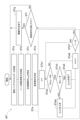
- FIG. 1 is a diagram for explaining a configuration example of a plasma processing system
- FIG. 1 is a diagram for explaining a configuration example of a capacitively coupled plasma processing apparatus
- FIG. 4 is an example timing chart associated with a plasma processing apparatus according to one exemplary embodiment
- 4 is a flow diagram of a control method according to one exemplary embodiment
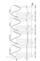
- Fig. 4 is a timing chart relating to a first example of determining the source frequency
- Fig. 4 is a timing chart related to a second example of determining the source frequency;
- FIG. 1 is a diagram for explaining a configuration example of a plasma processing system.
- a plasma processing system includes a plasma processing apparatus 1 and a main controller 2 .
- the plasma processing system is an example of a substrate processing system
- the plasma processing apparatus 1 is an example of a substrate processing apparatus.
- the plasma processing apparatus 1 includes a plasma processing chamber 10 , a substrate support section 11 and a plasma generation section 12 .
- Plasma processing chamber 10 has a plasma processing space.
- the plasma processing chamber 10 also has at least one gas inlet for supplying at least one process gas to the plasma processing space and at least one gas outlet for exhausting gas from the plasma processing space.
- the gas supply port is connected to a gas supply section 20, which will be described later, and the gas discharge port is connected to an exhaust system 40, which will be described later.
- the substrate support 11 is arranged in the plasma processing space and has a substrate support surface for supporting the substrate.
- the plasma generation unit 12 is configured to generate plasma from at least one processing gas supplied into the plasma processing space.
- Plasma formed in the plasma processing space includes capacitively coupled plasma (CCP), inductively coupled plasma (ICP), ECR plasma (Electron-Cyclotron-resonance plasma), helicon wave excited plasma (HWP: Helicon Wave Plasma), surface wave plasma (SWP: Surface Wave Plasma), or the like.
- the main controller 2 processes computer-executable instructions that cause the plasma processing apparatus 1 to perform the various steps described in this disclosure.
- Main controller 2 may be configured to control elements of plasma processing apparatus 1 to perform the various processes described herein. In one embodiment, part or all of the main controller 2 may be included in the plasma processing apparatus 1 .
- the main control unit 2 may include a processing unit 2a1, a storage unit 2a2, and a communication interface 2a3.
- the main controller 2 is implemented by, for example, a computer 2a.
- Processing unit 2a1 can be configured to perform various control operations by reading a program from storage unit 2a2 and executing the read program.
- the program includes computer-executable instructions that cause the plasma processing apparatus 1 to perform various steps of a control method according to exemplary embodiments described below.
- This program may be stored in the storage unit 2a2 in advance, or may be acquired via a medium when necessary.
- the acquired program is stored in the storage unit 2a2, read from the storage unit 2a2 and executed by the processing unit 2a1.
- the medium may be various storage media readable by the computer 2a, or may be a communication line connected to the communication interface 2a3.
- the processing unit 2a1 may be a CPU (Central Processing Unit).
- the storage unit 2a2 may include RAM (Random Access Memory), ROM (Read Only Memory), HDD (Hard Disk Drive), SSD (Solid State Drive), or a combination thereof.
- the communication interface 2a3 may communicate with the plasma processing apparatus 1 via a communication line such as a LAN (Local Area Network).
- FIG. 2 is a diagram for explaining a configuration example of a capacitively coupled plasma processing apparatus.
- the capacitively coupled plasma processing apparatus 1 includes a plasma processing chamber 10, a gas supply section 20, a power supply system 30 and an exhaust system 40. Further, the plasma processing apparatus 1 includes a substrate support section 11 and a gas introduction section. The gas introduction is configured to introduce at least one process gas into the plasma processing chamber 10 .
- the gas introduction section includes a showerhead 13 .
- a substrate support 11 is positioned within the plasma processing chamber 10 .
- the showerhead 13 is arranged above the substrate support 11 . In one embodiment, showerhead 13 forms at least a portion of the ceiling of plasma processing chamber 10 .
- the plasma processing chamber 10 has a plasma processing space 10 s defined by a showerhead 13 , side walls 10 a of the plasma processing chamber 10 and a substrate support 11 . Plasma processing chamber 10 is grounded.
- the showerhead 13 and substrate support 11 are electrically insulated from the housing of the plasma processing chamber 10 .
- the substrate support section 11 includes a body section 111 and a ring assembly 112 .
- the body portion 111 has a central region 111 a for supporting the substrate W and an annular region 111 b for supporting the ring assembly 112 .
- a wafer is an example of a substrate W;
- the annular region 111b of the body portion 111 surrounds the central region 111a of the body portion 111 in plan view.
- the substrate W is arranged on the central region 111 a of the main body 111
- the ring assembly 112 is arranged on the annular region 111 b of the main body 111 so as to surround the substrate W on the central region 111 a of the main body 111 .
- the central region 111a is also referred to as a substrate support surface for supporting the substrate W
- the annular region 111b is also referred to as a ring support surface for supporting the ring assembly 112.
- the body portion 111 includes a base 1110 and an electrostatic chuck 1111 .
- Base 1110 includes a conductive member.
- An electrostatic chuck 1111 is arranged on the base 1110 .
- the electrostatic chuck 1111 includes a ceramic member 1111a and an electrostatic electrode 1111b disposed within the ceramic member 1111a.
- Ceramic member 1111a has a central region 111a.
- the ceramic member 1111a also has an annular region 111b.
- another member surrounding the electrostatic chuck 1111 such as an annular electrostatic chuck or an annular insulating member, may have the annular region 111b.
- the ring assembly 112 may be placed on the annular electrostatic chuck or the annular insulating member, or may be placed on both the electrostatic chuck 1111 and the annular insulating member.
- Ring assembly 112 includes one or more annular members.
- the one or more annular members include one or more edge rings and at least one cover ring.
- the edge ring is made of a conductive material or an insulating material
- the cover ring is made of an insulating material.
- the substrate supporter 11 may include a temperature control module configured to adjust at least one of the electrostatic chuck 1111, the ring assembly 112, and the substrate to a target temperature.
- the temperature control module may include heaters, heat transfer media, channels 1110a, or combinations thereof.
- channels 1110 a are formed in base 1110 and one or more heaters are positioned in ceramic member 1111 a of electrostatic chuck 1111 .
- the substrate support 11 may also include a heat transfer gas supply configured to supply a heat transfer gas to the gap between the back surface of the substrate W and the central region 111a.
- the showerhead 13 is configured to introduce at least one processing gas from the gas supply unit 20 into the plasma processing space 10s.
- the showerhead 13 has at least one gas supply port 13a, at least one gas diffusion chamber 13b, and multiple gas introduction ports 13c.
- the processing gas supplied to the gas supply port 13a passes through the gas diffusion chamber 13b and is introduced into the plasma processing space 10s through a plurality of gas introduction ports 13c.
- showerhead 13 also includes at least one upper electrode.
- the gas introduction part may include one or more side gas injectors (SGI: Side Gas Injector) attached to one or more openings formed in the side wall 10a.
- SGI Side Gas Injector
- the gas supply unit 20 may include at least one gas source 21 and at least one flow controller 22 .
- gas supply 20 is configured to supply at least one process gas from respective gas sources 21 through respective flow controllers 22 to showerhead 13 .
- Each flow controller 22 may include, for example, a mass flow controller or a pressure controlled flow controller.
- gas supply 20 may include at least one flow modulation device for modulating or pulsing the flow rate of at least one process gas.
- the exhaust system 40 may be connected to a gas exhaust port 10e provided at the bottom of the plasma processing chamber 10, for example.
- Exhaust system 40 may include a pressure regulating valve and a vacuum pump.
- the pressure regulating valve regulates the pressure in the plasma processing space 10s.
- Vacuum pumps may include turbomolecular pumps, dry pumps, or combinations thereof.
- Power supply system 30 includes a high frequency power supply 31 and a bias power supply 32 .
- the high-frequency power supply 31 constitutes the plasma generator 12 of one embodiment.
- the radio frequency power supply 31 is configured to generate source radio frequency power RF.
- the source radio frequency power RF has a source frequency f RF . That is, the source RF power RF has a sinusoidal waveform whose frequency is the source frequency fRF .
- the source frequency f RF can be a frequency within the range of 10 MHz to 150 MHz.
- the high-frequency power supply 31 is electrically connected to the high-frequency electrode via a matching box 33, and is configured to supply source high-frequency power RF to the high-frequency electrode.
- the high-frequency electrode may be a conductive member of the base 1110, at least one electrode provided within the ceramic member 1111a, or an upper electrode.
- Matching box 33 has a variable impedance. The variable impedance of matcher 33 is set to reduce the reflection of source high frequency power RF from the load. Plasma is generated from the gases in the chamber 10 when the source radio frequency power RF is supplied to the radio frequency electrode.
- the bias power supply 32 is configured to generate electrical bias energy BE.
- a bias power supply 32 is electrically coupled to the substrate support 11 .
- the bias power supply 32 is electrically connected to the bias electrodes in the substrate support 11 and is configured to supply electrical bias energy BE to the bias electrodes.
- the bias electrode may be at least one electrode provided within the conductive member of the base 1110 or the ceramic member 1111a. Ions from the plasma are attracted to the substrate W when electrical bias energy BE is supplied to the bias electrode.
- the electric bias energy BE has a bias frequency.
- the bias frequency is lower than the source frequency.
- the bias frequency may be a frequency in the range of 100 kHz to 60 MHz, for example 400 kHz.
- the electrical bias energy BE is periodically supplied to the bias electrode in a bias period (time interval) or waveform period having a time length that is the reciprocal of the bias frequency, ie period CY.
- the electrical bias energy BE may be bias radio frequency power LF having a bias frequency. That is, the electrical bias energy BE may have a sinusoidal waveform whose frequency is the bias frequency.
- the bias power supply 32 is electrically connected to the bias electrode through the matching device 34 .
- the variable impedance of matching box 34 is set to reduce the reflection of bias high frequency power LF from the load.
- the electrical bias energy BE may include voltage pulses PV.
- the waveform of the pulse PV in the electrical bias energy BE can have a square wave, triangular wave, or arbitrary waveform.
- the polarity of the voltage of the pulse PV of electrical bias energy BE is set such that ions from the plasma can be drawn into the substrate W by creating a potential difference between the substrate W and the plasma.
- the pulse PV of electrical bias energy BE may, in one example, be a pulse of negative voltage.
- a pulse PV of the electrical bias energy BE may be generated by waveform shaping using a pulse unit for a DC voltage from a DC power supply. If the electrical bias energy BE is a voltage pulse PV, the matching device 34 is not required.
- the high-frequency power supply 31 is configured to supply the source high-frequency power RF during the period in which the cycle CY is repeated, that is, during the period in which the electrical bias energy BE is periodically supplied.
- RF power supply 31 is configured to generate source RF power RF having a source frequency f RF set to reduce reflected waves from a load of source RF power RF in each of a plurality of phase periods SP within period CY. It is configured.
- the multiple phase periods SP are multiple periods dividing the cycle CY. Note that the source frequency f RF initially used in each of the plurality of phase periods SP within the period CY is determined in advance. That is, initially the set of source frequencies f RF used in the phase periods SP within the period CY is predetermined. The details of determining the source frequency f RF initially used in each of the phase periods SP within the period CY will be described later.
- the RF power supply 31 synchronizes with the bias power supply 32 using a synchronization signal for setting the source frequency f RF for each of the multiple phase periods SP.
- the synchronization signal may be supplied from the high frequency power supply 31 to the bias power supply 32 or may be supplied from the bias power supply 32 to the high frequency power supply 31 .
- synchronization signals may be provided to the high frequency power supply 31 and the bias power supply 32 from other devices.
- the plasma processing apparatus 1 further includes a sensor 35 (first sensor) and a sensor 36 (second sensor).
- the sensor 35 is arranged to measure the power level Pr of the reflected wave from the load of the source radio frequency power RF.
- Sensor 35 includes, for example, a directional coupler. This directional coupler may be provided between the high frequency power supply 31 and the matching device 33 .
- the sensor 35 may be configured to further measure the power level Pf of the traveling wave of the source high frequency power RF.
- the power level Pr of the reflected wave measured by the sensor 35 is notified to the high frequency power supply 31 .
- the power level Pf of the traveling wave may be notified from the sensor 35 to the high frequency power supply 31 .
- Sensors 36 include voltage sensors and current sensors.
- the sensor 36 is arranged to measure the voltage V RF and the current I RF in the feed line connecting the RF power supply 31 and the RF electrode together.
- Source high frequency power RF is supplied to the high frequency electrode via this feed line.
- the sensor 36 may be provided between the high frequency power supply 31 and the matching box 33 .
- the voltage V RF and the current I RF in the feed line are communicated to the RF power supply 31 .
- the high-frequency power supply 31 specifies the phase period SP MIN (see FIG. 3) having the minimum value of the power level Pr of the reflected wave among the plurality of phase periods SP within the cycle CY.
- the high frequency power supply 31 determines the phase difference between the voltage V RF and the current I RF in the phase period SP MIN as the reference value ⁇ .
- the high-frequency power supply 31 generates the phase difference ⁇ between the voltage V RF and the current I RF in each of the phase periods SP and the reference value ⁇ for each of the phase periods SP. , i.e., set the source frequency f RF for each of a plurality of phase periods SP.
- the frequency control increases the source frequency f RF when the phase difference ⁇ between the voltage V RF and the current I RF is greater than the reference value ⁇ in each of the multiple phase periods SP. good too. That is, the frequency control changes f RF to f RF + ⁇ f when the phase difference ⁇ between the voltage V RF and the current I RF is greater than the reference value ⁇ in each of the phase periods SP. good too.
- the frequency control may also reduce the source frequency f RF when the phase difference ⁇ is less than the reference value ⁇ . That is, the frequency control changes f RF to f RF ⁇ f when the phase difference ⁇ between the voltage V RF and the current I RF is smaller than the reference value ⁇ in each of a plurality of phase periods SP.
- the high-frequency power supply 31 may use a predetermined fixed value as the adjustment amount ⁇ f of the source frequency f RF by frequency control in each of the plurality of phase periods SP.
- the high-frequency power supply 31 adjusts the adjustment amount ⁇ f of the source frequency f RF by frequency control according to the absolute value of the difference between the phase difference ⁇ and the reference value ⁇ in each of the plurality of phase periods SP. good too. That is, the high-frequency power supply may perform frequency control such that the adjustment amount ⁇ f of the source frequency fRF increases as the absolute value of the difference between the phase difference ⁇ and the reference value ⁇ increases.
- the high frequency power supply 31 may perform the above frequency control when the power level Pr of the reflected wave is greater than the threshold value Pth in each of a plurality of phase periods SP. Further, the high-frequency power supply 31 may lower the threshold Pth when all the power levels Pr of the reflected waves in each of the plurality of phase periods SP within the cycle CY are equal to or lower than the threshold Pth. The threshold Pth is lowered by Pth- ⁇ Pth. The decrease amount ⁇ Pth of the threshold value Pth may be determined in advance. Note that the high-frequency power supply 31 may lower the threshold Pth when the power level Pr of the reflected wave in each of all the phase periods SP of two or more consecutive cycles CY is equal to or less than the threshold Pth.
- the high frequency power supply 31 may include a signal generator 31g and an amplifier 31a.
- the signal generator 31g is configured to generate a high frequency signal.
- the amplifier 31a is configured to amplify the high frequency signal from the signal generator 31g to generate source high frequency power RF. Note that the synchronization signal described above may be supplied to the bias power supply 32 from the signal generator 31g.
- Signal generator 31g initially generates a high frequency signal having a predetermined source frequency f RF for each of a plurality of phase periods SP.
- the signal generator 31g also specifies the phase period SP MIN , determines the reference value ⁇ , and the high frequency signal having the source frequency f RF for each of the plurality of phase periods SP adjusted by the frequency control described above. generate a signal.
- signal generator 31g may include a processor and a D/A converter.
- the signal generator 31g may convert the digital signal output from the processor into a high frequency signal, that is, an analog signal in the D/A converter.
- a processor in signal generator 31g identifies the phase period SP MIN , determines the reference value ⁇ , and produces a digital signal having a source frequency f RF for each of the plurality of phase periods SP adjusted by the frequency control described above. may occur.
- the phase difference between the voltage V RF and the current I RF in the phase period SP MIN having the minimum value of the power level Pr of the reflected wave is determined as the reference value ⁇ . That is, a phase difference in which the influence of reflected waves that may contain intermodulation distortion components and harmonic components is reduced is obtained as the reference value ⁇ .
- the source frequency fRF is adjusted according to the comparison result between the phase difference ⁇ between the voltage VRF and the current IRF and the reference value ⁇ . As a result, the power level of the reflected wave of the source high frequency power RF is reduced.
- FIG. 4 is a flow diagram of a control method according to one exemplary embodiment.
- a control method (hereinafter referred to as “method MT”) shown in FIG. 4 can be applied to the plasma processing apparatus 1 .
- step STa electrical bias energy BE is supplied from the bias power supply 32 to the substrate supporting portion 11 .
- the electrical bias energy BE is supplied periodically with a period CY.
- step STb source high frequency power RF is supplied from the high frequency power supply 31 to the high frequency electrode in order to generate plasma from gas within the chamber 10 .
- the source frequency RF of the source radio frequency power RF used initially in each of the plurality of phase periods SP is predetermined as described above.
- step STc the phase period SP MIN is specified as described above. Then, in step STd, the reference value ⁇ is determined as described above.
- step STe frequency control for each of the plurality of phase periods SP according to the result of comparison between the phase difference ⁇ between the voltage VRF and the current IRF in each of the plurality of phase periods SP and the reference value ⁇ . is done. That is, the source frequency f RF of the source high-frequency power RF for each of the phase periods SP is set according to the comparison result between the phase difference ⁇ and the reference value ⁇ in each of the phase periods SP.
- the frequency control may increase the source frequency f RF when the phase difference ⁇ is greater than the reference value ⁇ in each of the plurality of phase periods SP, as described above, and the phase difference ⁇ is greater than the reference value ⁇ . If is also small, the source frequency f RF may be lowered.
- the step STe may include steps STe1 to STe7, as shown in FIG.
- n is set to 1.
- Pth the threshold value
- Pr(n) is the power level Pr of the reflected wave in the n-th phase period SP(n) among the plurality of phase periods SP within the period CY.
- step STe2 If it is determined in step STe2 that the power level Pr(n) of the reflected wave is equal to or lower than the threshold value Pth, the process proceeds to step STe6. On the other hand, when it is determined in step STe2 that the power level Pr(n) of the reflected wave is greater than the threshold value Pth, the process proceeds to step STe3. Note that the method MT may not include the step STe2.
- step STe3 it is determined whether or not the phase difference ⁇ (n) is greater than the reference value ⁇ .
- ⁇ (n) is the phase difference ⁇ between the voltage V RF and the current I RF in the n-th phase period SP(n) among the plurality of phase periods SP within the period CY.
- step STe3 If the phase difference ⁇ (n) is determined to be greater than the reference value ⁇ in step STe3, the source frequency f RF (n) is increased in step STe4. Note that f RF (n) is the source frequency f RF for the n-th phase period SP(n) of the plurality of phase periods SP in period CY. On the other hand, if it is determined in step STe3 that the phase difference ⁇ (n) is smaller than the reference value ⁇ , the source frequency f RF (n) is lowered in step STe5.
- step STe6 n is incremented by one. Then, in step STe7, it is determined whether or not n is greater than N. N is the number of phase periods SP in the period CY. If n is N or less, the process from step STe2 is repeated. On the other hand, if n is greater than N, the process proceeds to step STf.
- step STf it is determined whether or not the update conditions are satisfied.
- the update condition is satisfied when all the power levels Pr of the reflected waves in each of a plurality of phase periods SP within the cycle CY are equal to or less than the threshold value Pth.
- the update condition may be satisfied when the power level Pr of the reflected wave in each of all phase periods SP of two or more consecutive cycles CY is equal to or less than the threshold value Pth. If the update condition is satisfied, the threshold Pth is lowered in step STg.
- step STg If the update condition is not satisfied, or after the threshold Pth is lowered in step STg, the process proceeds to step STa. Note that the method MT may not include the step STf and the step STg.
- step STa electric bias energy is supplied in the next cycle CY, and in step STb, source high-frequency power RF is supplied in this cycle CY.
- step STb source radio frequency power RF is supplied having a source frequency f RF for each of the plurality of phase periods SP set in step STe. Then, the processing from step STc is continued.
- Such a method MT terminates when a termination condition is satisfied.
- a termination condition may be specified in the recipe data.
- determining the source frequency f RF initially used in each of the phase periods SP within the period CY is performed by the RF power supply 31 (or its processor).
- the determination of the source frequency f RF may be made by the processor of signal generator 31g. Determination of the source frequency f RF may be made by a separate controller.
- FIG. 5 is a timing chart relating to a first example of determining the source frequency.
- the source frequency f RF is adjusted during overlapping periods during which both the electrical bias energy BE and the source RF power RF are supplied.
- the overlapping period includes a plurality of cycles CY, namely M cycles CY(1) to CY(M), as shown in FIG.
- Each of the multiple cycles CY includes multiple phase periods SP, namely N phase periods SP(1) to SP(N).
- phase period SP(n) represents the n-th phase period among phase periods SP(1) to SP(N).
- the phase period SP(m,n) represents the n-th phase period SP(n) in the m-th cycle CY(m).
- the high frequency power supply 31 generates the representative value RV from the measured values in each of the multiple phase periods SP.
- the measurement may be the power level Pr of the reflected wave obtained by sensor 35 .
- the measured value may be the value of the ratio of the power level Pr of the reflected wave to the output power level of the source radio frequency power RF.
- the measurement may be the phase difference between voltage and current obtained by sensor 36 in each of the plurality of phase periods SP.
- the representative value RV may be the average value or maximum value of the measured values in each of the plurality of phase periods SP.
- the representative value RV(n) represents the representative value RV acquired in the n-th phase period SP(n) among the phase periods SP(1) to SP(N).
- the representative value RV(m, n) represents the representative value RV acquired in the n-th phase period within the m-th cycle CY.
- the high-frequency power supply 31 sets the source frequency fRF of the source high-frequency power RF used in the same phase period SP(n) of a plurality of cycles CY to a plurality of mutually different frequencies.
- the high-frequency power supply 31 compares the representative values RV(n) obtained in the same phase period SP(n) of a plurality of cycles CY, and determines the frequency at which the reflection of the source high-frequency power RF is most suppressed among the plurality of frequencies. to select.
- the high frequency power supply 31 selects a frequency that minimizes the power level Pr of the reflected wave of the source high frequency power RF.
- the radio frequency power supply 31 determines the selected frequency as the source frequency f RF for the phase period SP(n) in the subsequent cycle CY.
- FIG. 6 is a timing chart relating to a second example of determining the source frequency.
- the high-frequency power supply 31 generates the source high-frequency power RF at the source frequency f It is configured to adjust RF according to changes in the representative value RV(n).
- the change in the representative value RV(n) is determined by using different frequencies of the source RF power RF in corresponding phase periods SP(n) in each of the two or more periods CY preceding the period CY(m). .
- Two or more cycles CY before cycle CY(m) include a first cycle and a second cycle.
- the first period is the period CY(mQ(2))
- the second period is the period after the first period
- Q(1) is an integer of 1 or more
- Q(2) is an integer of 2 or more
- Q(1) ⁇ Q(2) is satisfied.
- the high frequency power supply 31 applies the frequency f(mQ(1),n) of the source high frequency power RF in the phase period SP(mQ(1),n) to the phase period SP(mQ(2),n ) from the frequency of the source RF power RF.
- f(m,n) represents the frequency of the source RF power RF used in the phase period SP(m,n).
- ⁇ (m,n) represents the amount of frequency shift.
- One frequency shift is one of a frequency decrease and a frequency increase. If one frequency shift is a decrease in frequency, ⁇ (m,n) has a negative value. If one frequency shift is an increase in frequency, ⁇ (m,n) has a positive value.
- the frequencies of the source high-frequency power RF in each of the plurality of phase periods SP in the cycle CY (mQ(2)) are the same as f0 , but may be different.
- the frequencies of the source high frequency power RF in each of the plurality of phase periods SP in the cycle CY (mQ(1)) are the same as each other, and are set to frequencies reduced from the frequency f0 . , but may be increased from frequency f0 .
- the high-frequency power supply 31 increases or decreases the degree of reflection of the source high-frequency power RF (for example, the power level Pr of the reflected wave) due to the frequency shift, the representative value RV (m ⁇ Q(2), n) and the representative value RV(m ⁇ Q(1), n). If the degree of reflection of the source high frequency power RF is reduced due to one frequency shift, the high frequency power supply 31 changes the frequency f(m,n) to the frequency f(mQ(1),n) as set to a frequency with one frequency shift.
- the degree of reflection of the source high frequency power RF for example, the power level Pr of the reflected wave
- the amount of one frequency shift ⁇ (m,n) in the phase period SP(m,n) is the amount of one frequency shift ⁇ (mQ(1) in the phase period SP(mQ(1),n) ) and n). That is, the absolute value of the frequency shift amount ⁇ (m,n) may be the same as the frequency shift amount ⁇ (m ⁇ Q(1),n). Alternatively, the absolute value of the frequency shift amount ⁇ (m,n) may be greater than the frequency shift amount ⁇ (m ⁇ Q(1),n). Alternatively, the absolute value of the frequency shift amount ⁇ (m,n) may be set so that it increases as the degree of reflection in the phase period SP(m ⁇ Q(1),n) increases. For example, the absolute value of the amount of frequency shift ⁇ (m,n) may be determined as a function of the degree of reflection.
- a frequency shift on one side may increase the degree of reflection of the source high frequency power RF.
- the high frequency power supply 31 may set the frequency f(m,n) to a frequency having the other frequency shift with respect to the frequency f(mQ(1),n).
- the frequency of the source high-frequency power RF in the phase period SP(n) of each of the two or more cycles before the cycle CY(m) is the frequency of the source high-frequency power RF in the phase period SP(n) of the previous cycle. It may be updated to have one frequency shift with respect to frequency.
- the other frequency shift is in the phase period of the cycle CY(m)
- the source radio frequency power of SP(n) may be applied at the frequency of RF.
- the frequency of the source high-frequency power RF in the phase period SP(n) of the period CY(m) is the frequency having the other frequency shift with respect to the frequency of the source high-frequency power in the earliest period among the two or more periods. may be set to
- the high frequency power supply 31 may set the frequency of the source high frequency power RF in the phase period SP(n) within the period CY(m+Q(1)) to an intermediate frequency.
- Cycle CY(m+Q(1)) is the third cycle after cycle CY(m).
- the intermediate frequencies that can be set in the phase period SP(m+Q(1),n) are the frequencies between f(m ⁇ Q(1),n) and f(m,n), f(m ⁇ It may be the average value of Q(1),n) and f(m,n).
- a case may occur where the degree of reflection of the source high-frequency power RF (for example, the power level Pr of the reflected wave) when using an intermediate frequency in the phase period SP (m+Q(1), n) becomes greater than a predetermined threshold.
- the high frequency power supply 31 sets the frequency of the source high frequency power RF in the phase period SP(n) within the period CY(m+Q(2)) to a frequency having the other frequency shift with respect to the intermediate frequency.
- Cycle CY(m+Q(2)) is the fourth cycle after cycle CY(m+Q(2)).
- a threshold is predetermined.
- the absolute value of the other frequency shift amount ⁇ (m+Q(2),n) is greater than the absolute value of the one frequency shift amount ⁇ (m,n).
- the threshold values for each of the plurality of phase periods SP in each of the plurality of cycles CY may be the same or different.
- the frequency of the source RF power RF set for each of the phase periods SP(1)-SP(N) of the period CY(M) is is determined as the respective source frequency f RF .
- the frequency determined by adding each of the plurality of frequency offsets and the reference frequency in each phase period SP within the cycle CY is used as the source frequency f RF of the source high frequency power RF.
- Each of the multiple frequency offsets has a positive or negative value.
- a frequency offset for each phase period SP is then determined that maximizes the power level of the source RF power RF delivered to the plasma.
- the power level of the source high-frequency power RF transmitted to the plasma can be the difference between the power level of the traveling wave of the source high-frequency power RF and the power level of the reflected wave.
- the determined frequency offsets for each of the multiple phase periods SP are stored in a table.
- the high frequency power supply 31 uses the frequency determined by adding the reference frequency and the corresponding frequency offset stored in the table as the source frequency f RF of the source high frequency power RF in each phase period SP within each period CY. .
- the plasma processing apparatus may be an inductively coupled plasma processing apparatus, an ECR plasma processing apparatus, a helicon wave excited plasma processing apparatus, or a surface wave plasma processing apparatus.
- source high frequency power RF is used for plasma generation.
- the phase difference between the voltage and the current in the phase period with the minimum power level of the reflected wave is determined as the reference value. That is, a phase difference in which the influence of reflected waves that may contain intermodulation distortion components and harmonic components is reduced is obtained as a reference value. Then, in each of the plurality of phase periods, the source frequency is adjusted according to the comparison result of the phase difference between the voltage and current and the reference value. As a result, the power level of the reflected wave of the source RF power is reduced.
- the frequency control increases the source frequency when the phase difference between the voltage and the current in the feedline is greater than the reference value in each of the plurality of phase periods;
- the plasma processing apparatus of E1 wherein the source frequency is reduced when the phase difference is less than the reference value.
- the high-frequency power supply is configured to adjust the amount of adjustment of the source frequency by the frequency control in each of the plurality of phase periods according to the absolute value of the difference between the phase difference and the reference value.
- the plasma processing apparatus according to E1 or E2.
- the high-frequency power supply reduces the threshold when all of the power levels of the reflected waves acquired by the first sensor in each of the plurality of phase periods within the bias period are equal to or less than the threshold, to E4.
- the high frequency power source comprises a signal generator configured to generate a high frequency signal; an amplifier configured to amplify the radio frequency signal to generate the source radio frequency power; including The signal generator is identifying the phase period having the minimum value of the power level of the reflected wave; determining the reference value; generating the high frequency signal having the source frequency for each of the plurality of phase periods adjusted by the frequency control; configured as The plasma processing apparatus according to any one of E1 to E5.
- E7 The electrical bias energy of any one of E1 to E6, wherein the electrical bias energy is a bias RF power having the bias frequency or a pulse of voltage generated periodically at time intervals that are the reciprocal of the bias frequency. plasma processing equipment.
- the plasma processing apparatus is a capacitively coupled plasma processing apparatus,
- the high-frequency electrode is provided within the substrate support or is an upper electrode provided above the substrate support,
- the plasma processing apparatus according to any one of E1 to E7.
- a bias power supply configured to generate electrical bias energy supplied to a substrate support provided within a chamber of the plasma processing apparatus, the electrical bias energy having a bias frequency, the reciprocal of the bias frequency.
- the bias power supply which is generated periodically with a bias period having a time length of a radio frequency power supply configured to generate a source radio frequency power supplied to a radio frequency electrode to generate a plasma from gas within the chamber; with The high-frequency power source identifying a phase period having a minimum power level of a reflected wave of the source high-frequency power among a plurality of phase periods within the bias period; determining, as a reference value, the phase difference between the voltage and current in the feed line between the high-frequency power supply and the high-frequency electrode in the identified phase period; the source RF power for each of the plurality of phase periods according to a comparison of the phase difference between the voltage and the current in the feedline in each of the plurality of phase periods to the reference value; frequency control, which sets the source frequency of the configured as power system.
- the frequency control increases the source frequency when the phase difference between the voltage and the current in the feedline is greater than the reference value in each of the plurality of phase periods;
- the frequency control increases the source frequency when the phase difference between the voltage and the current in the feedline is greater than the reference value in each of the plurality of phase periods;
- Plasma processing apparatus 10
- Chamber 11
- Substrate support 30
- Power supply system 31
- High frequency power supply 32
- Bias power supply 35
- Sensor 36
- Sensor 36
Landscapes
- Physics & Mathematics (AREA)
- Engineering & Computer Science (AREA)
- Chemical & Material Sciences (AREA)
- Plasma & Fusion (AREA)
- Analytical Chemistry (AREA)
- Spectroscopy & Molecular Physics (AREA)
- Electromagnetism (AREA)
- General Chemical & Material Sciences (AREA)
- Chemical Kinetics & Catalysis (AREA)
- Materials Engineering (AREA)
- Mechanical Engineering (AREA)
- Metallurgy (AREA)
- Organic Chemistry (AREA)
- Drying Of Semiconductors (AREA)
- Plasma Technology (AREA)
Priority Applications (4)
| Application Number | Priority Date | Filing Date | Title |
|---|---|---|---|
| KR1020247019319A KR20240101662A (ko) | 2021-11-19 | 2022-11-10 | 플라즈마 처리 장치, 전원 시스템, 제어 방법, 프로그램, 및 기억 매체 |
| JP2023561565A JP7622252B2 (ja) | 2021-11-19 | 2022-11-10 | プラズマ処理装置、電源システム、制御方法、プログラム、及び記憶媒体 |
| CN202280074030.XA CN118202792A (zh) | 2021-11-19 | 2022-11-10 | 等离子体处理装置、电源系统、控制方法、程序和存储介质 |
| US18/607,327 US12476080B2 (en) | 2021-11-19 | 2024-03-15 | Plasma processing apparatus, power supply system, control method, program, and storage medium |
Applications Claiming Priority (2)
| Application Number | Priority Date | Filing Date | Title |
|---|---|---|---|
| JP2021188303 | 2021-11-19 | ||
| JP2021-188303 | 2021-11-19 |
Related Child Applications (1)
| Application Number | Title | Priority Date | Filing Date |
|---|---|---|---|
| US18/607,327 Continuation US12476080B2 (en) | 2021-11-19 | 2024-03-15 | Plasma processing apparatus, power supply system, control method, program, and storage medium |
Publications (1)
| Publication Number | Publication Date |
|---|---|
| WO2023090256A1 true WO2023090256A1 (ja) | 2023-05-25 |
Family
ID=86396925
Family Applications (1)
| Application Number | Title | Priority Date | Filing Date |
|---|---|---|---|
| PCT/JP2022/041985 Ceased WO2023090256A1 (ja) | 2021-11-19 | 2022-11-10 | プラズマ処理装置、電源システム、制御方法、プログラム、及び記憶媒体 |
Country Status (6)
| Country | Link |
|---|---|
| US (1) | US12476080B2 (https=) |
| JP (1) | JP7622252B2 (https=) |
| KR (1) | KR20240101662A (https=) |
| CN (1) | CN118202792A (https=) |
| TW (1) | TW202336804A (https=) |
| WO (1) | WO2023090256A1 (https=) |
Cited By (2)
| Publication number | Priority date | Publication date | Assignee | Title |
|---|---|---|---|---|
| US20230369020A1 (en) * | 2021-01-29 | 2023-11-16 | Tokyo Electron Limited | Plasma processing apparatus and method for controlling source frequency of source radio-frequency power |
| CN120077469A (zh) * | 2023-09-29 | 2025-05-30 | 东京毅力科创株式会社 | 等离子体处理装置和控制方法 |
Citations (3)
| Publication number | Priority date | Publication date | Assignee | Title |
|---|---|---|---|---|
| JP2006286254A (ja) * | 2005-03-31 | 2006-10-19 | Daihen Corp | 高周波電源装置 |
| JP2018536295A (ja) * | 2015-09-01 | 2018-12-06 | エムケーエス インストゥルメンツ,インコーポレイテッド | プラズマrfバイアス消去システム |
| JP2021106354A (ja) * | 2019-12-27 | 2021-07-26 | 株式会社ダイヘン | 高周波電源システム |
Family Cites Families (2)
| Publication number | Priority date | Publication date | Assignee | Title |
|---|---|---|---|---|
| JP5319150B2 (ja) | 2008-03-31 | 2013-10-16 | 東京エレクトロン株式会社 | プラズマ処理装置及びプラズマ処理方法及びコンピュータ読み取り可能な記憶媒体 |
| JP6928407B1 (ja) * | 2021-03-15 | 2021-09-01 | 株式会社アドテックプラズマテクノロジー | 出力する高周波電力の経時変化パターンを任意に設定可能な高周波電源 |
-
2022
- 2022-11-07 TW TW111142393A patent/TW202336804A/zh unknown
- 2022-11-10 JP JP2023561565A patent/JP7622252B2/ja active Active
- 2022-11-10 WO PCT/JP2022/041985 patent/WO2023090256A1/ja not_active Ceased
- 2022-11-10 KR KR1020247019319A patent/KR20240101662A/ko active Pending
- 2022-11-10 CN CN202280074030.XA patent/CN118202792A/zh active Pending
-
2024
- 2024-03-15 US US18/607,327 patent/US12476080B2/en active Active
Patent Citations (3)
| Publication number | Priority date | Publication date | Assignee | Title |
|---|---|---|---|---|
| JP2006286254A (ja) * | 2005-03-31 | 2006-10-19 | Daihen Corp | 高周波電源装置 |
| JP2018536295A (ja) * | 2015-09-01 | 2018-12-06 | エムケーエス インストゥルメンツ,インコーポレイテッド | プラズマrfバイアス消去システム |
| JP2021106354A (ja) * | 2019-12-27 | 2021-07-26 | 株式会社ダイヘン | 高周波電源システム |
Cited By (4)
| Publication number | Priority date | Publication date | Assignee | Title |
|---|---|---|---|---|
| US20230369020A1 (en) * | 2021-01-29 | 2023-11-16 | Tokyo Electron Limited | Plasma processing apparatus and method for controlling source frequency of source radio-frequency power |
| US12362144B2 (en) * | 2021-01-29 | 2025-07-15 | Tokyo Electron Limited | Plasma processing apparatus and method for controlling source frequency of source radio-frequency power |
| US20250308851A1 (en) * | 2021-01-29 | 2025-10-02 | Tokyo Electron Limited | Plasma processing apparatus and method for controlling source frequency of source radio-frequency power |
| CN120077469A (zh) * | 2023-09-29 | 2025-05-30 | 东京毅力科创株式会社 | 等离子体处理装置和控制方法 |
Also Published As
| Publication number | Publication date |
|---|---|
| US12476080B2 (en) | 2025-11-18 |
| JP7622252B2 (ja) | 2025-01-27 |
| JPWO2023090256A1 (https=) | 2023-05-25 |
| US20240222078A1 (en) | 2024-07-04 |
| TW202336804A (zh) | 2023-09-16 |
| CN118202792A (zh) | 2024-06-14 |
| KR20240101662A (ko) | 2024-07-02 |
Similar Documents
| Publication | Publication Date | Title |
|---|---|---|
| JP7638168B2 (ja) | プラズマ処理装置及びプラズマ処理方法 | |
| WO2023132300A1 (ja) | プラズマ処理装置、電源システム、制御方法、プログラム、及び記憶媒体 | |
| US20250308851A1 (en) | Plasma processing apparatus and method for controlling source frequency of source radio-frequency power | |
| US12249487B2 (en) | Plasma processing apparatus and plasma processing method | |
| US20250149296A1 (en) | Plasma processing apparatus and plasma processing method | |
| US12476080B2 (en) | Plasma processing apparatus, power supply system, control method, program, and storage medium | |
| WO2023127655A1 (ja) | プラズマ処理装置、電源システム、制御方法、プログラム、及び記憶媒体 | |
| JP7756056B2 (ja) | エッチング方法及びプラズマ処理装置 | |
| WO2024014398A1 (ja) | プラズマ処理装置及びプラズマ処理方法 | |
| JP7678233B2 (ja) | プラズマ処理装置、ソース高周波電力のソース周波数を制御する方法、及び記憶媒体 | |
| CN120457773A (zh) | 等离子体处理装置和等离子体处理方法 | |
| JP2023129234A (ja) | プラズマ処理装置 | |
| KR20220163300A (ko) | 플라즈마 처리 장치 및 플라즈마 처리 방법 | |
| WO2023074816A1 (ja) | プラズマ処理装置、給電システム、制御方法、プログラム、及び記憶媒体 | |
| CN120188575B (zh) | 等离子体处理装置、电源系统和控制生成源频率的方法 | |
| US20250266248A1 (en) | Electric bias control in plasma processing | |
| WO2024062804A1 (ja) | プラズマ処理装置及びプラズマ処理方法 | |
| WO2024106257A1 (ja) | プラズマ処理装置及びプラズマ処理方法 | |
| WO2025057636A1 (ja) | プラズマ処理装置 | |
| JP2024119243A (ja) | プラズマ処理装置、電源システム、及びプラズマ処理方法 | |
| TW202442033A (zh) | 電漿處理裝置、電源系統及頻率控制方法 |
Legal Events
| Date | Code | Title | Description |
|---|---|---|---|
| 121 | Ep: the epo has been informed by wipo that ep was designated in this application |
Ref document number: 22895538 Country of ref document: EP Kind code of ref document: A1 |
|
| ENP | Entry into the national phase |
Ref document number: 2023561565 Country of ref document: JP Kind code of ref document: A |
|
| WWE | Wipo information: entry into national phase |
Ref document number: 202280074030.X Country of ref document: CN |
|
| WWE | Wipo information: entry into national phase |
Ref document number: 1020247019319 Country of ref document: KR |
|
| NENP | Non-entry into the national phase |
Ref country code: DE |
|
| 122 | Ep: pct application non-entry in european phase |
Ref document number: 22895538 Country of ref document: EP Kind code of ref document: A1 |