WO2023089923A1 - ブランキングアパーチャアレイシステム及び荷電粒子ビーム描画装置 - Google Patents
ブランキングアパーチャアレイシステム及び荷電粒子ビーム描画装置 Download PDFInfo
- Publication number
- WO2023089923A1 WO2023089923A1 PCT/JP2022/033750 JP2022033750W WO2023089923A1 WO 2023089923 A1 WO2023089923 A1 WO 2023089923A1 JP 2022033750 W JP2022033750 W JP 2022033750W WO 2023089923 A1 WO2023089923 A1 WO 2023089923A1
- Authority
- WO
- WIPO (PCT)
- Prior art keywords
- data
- error detection
- register
- detection code
- aperture array
- Prior art date
- Legal status (The legal status is an assumption and is not a legal conclusion. Google has not performed a legal analysis and makes no representation as to the accuracy of the status listed.)
- Ceased
Links
Images



Classifications
-
- H—ELECTRICITY
- H01—ELECTRIC ELEMENTS
- H01J—ELECTRIC DISCHARGE TUBES OR DISCHARGE LAMPS
- H01J37/00—Discharge tubes with provision for introducing objects or material to be exposed to the discharge, e.g. for the purpose of examination or processing thereof
- H01J37/30—Electron-beam or ion-beam tubes for localised treatment of objects
- H01J37/3002—Details
- H01J37/3007—Electron or ion-optical systems
-
- H—ELECTRICITY
- H01—ELECTRIC ELEMENTS
- H01J—ELECTRIC DISCHARGE TUBES OR DISCHARGE LAMPS
- H01J37/00—Discharge tubes with provision for introducing objects or material to be exposed to the discharge, e.g. for the purpose of examination or processing thereof
- H01J37/30—Electron-beam or ion-beam tubes for localised treatment of objects
- H01J37/317—Electron-beam or ion-beam tubes for localised treatment of objects for changing properties of the objects or for applying thin layers thereon, e.g. for ion implantation
- H01J37/3174—Particle-beam lithography, e.g. electron beam lithography
- H01J37/3177—Multi-beam, e.g. fly's eye, comb probe
-
- G—PHYSICS
- G03—PHOTOGRAPHY; CINEMATOGRAPHY; ANALOGOUS TECHNIQUES USING WAVES OTHER THAN OPTICAL WAVES; ELECTROGRAPHY; HOLOGRAPHY
- G03F—PHOTOMECHANICAL PRODUCTION OF TEXTURED OR PATTERNED SURFACES, e.g. FOR PRINTING, FOR PROCESSING OF SEMICONDUCTOR DEVICES; MATERIALS THEREFOR; ORIGINALS THEREFOR; APPARATUS SPECIALLY ADAPTED THEREFOR
- G03F7/00—Photomechanical, e.g. photolithographic, production of textured or patterned surfaces, e.g. printing surfaces; Materials therefor, e.g. comprising photoresists; Apparatus specially adapted therefor
- G03F7/20—Exposure; Apparatus therefor
-
- H—ELECTRICITY
- H01—ELECTRIC ELEMENTS
- H01J—ELECTRIC DISCHARGE TUBES OR DISCHARGE LAMPS
- H01J37/00—Discharge tubes with provision for introducing objects or material to be exposed to the discharge, e.g. for the purpose of examination or processing thereof
- H01J37/02—Details
- H01J37/04—Arrangements of electrodes and associated parts for generating or controlling the discharge, e.g. electron-optical arrangement or ion-optical arrangement
- H01J37/045—Beam blanking or chopping, i.e. arrangements for momentarily interrupting exposure to the discharge
-
- H—ELECTRICITY
- H01—ELECTRIC ELEMENTS
- H01J—ELECTRIC DISCHARGE TUBES OR DISCHARGE LAMPS
- H01J37/00—Discharge tubes with provision for introducing objects or material to be exposed to the discharge, e.g. for the purpose of examination or processing thereof
- H01J37/02—Details
- H01J37/24—Circuit arrangements not adapted to a particular application of the tube and not otherwise provided for
-
- H—ELECTRICITY
- H01—ELECTRIC ELEMENTS
- H01J—ELECTRIC DISCHARGE TUBES OR DISCHARGE LAMPS
- H01J37/00—Discharge tubes with provision for introducing objects or material to be exposed to the discharge, e.g. for the purpose of examination or processing thereof
- H01J37/30—Electron-beam or ion-beam tubes for localised treatment of objects
- H01J37/304—Controlling tubes by information coming from the objects or from the beam, e.g. correction signals
-
- H—ELECTRICITY
- H10—SEMICONDUCTOR DEVICES; ELECTRIC SOLID-STATE DEVICES NOT OTHERWISE PROVIDED FOR
- H10P—GENERIC PROCESSES OR APPARATUS FOR THE MANUFACTURE OR TREATMENT OF DEVICES COVERED BY CLASS H10
- H10P76/00—Manufacture or treatment of masks on semiconductor bodies, e.g. by lithography or photolithography
-
- H—ELECTRICITY
- H01—ELECTRIC ELEMENTS
- H01J—ELECTRIC DISCHARGE TUBES OR DISCHARGE LAMPS
- H01J2237/00—Discharge tubes exposing object to beam, e.g. for analysis treatment, etching, imaging
- H01J2237/04—Means for controlling the discharge
- H01J2237/043—Beam blanking
- H01J2237/0435—Multi-aperture
-
- H—ELECTRICITY
- H01—ELECTRIC ELEMENTS
- H01J—ELECTRIC DISCHARGE TUBES OR DISCHARGE LAMPS
- H01J2237/00—Discharge tubes exposing object to beam, e.g. for analysis treatment, etching, imaging
- H01J2237/04—Means for controlling the discharge
- H01J2237/043—Beam blanking
- H01J2237/0435—Multi-aperture
- H01J2237/0437—Semiconductor substrate
-
- H—ELECTRICITY
- H01—ELECTRIC ELEMENTS
- H01J—ELECTRIC DISCHARGE TUBES OR DISCHARGE LAMPS
- H01J2237/00—Discharge tubes exposing object to beam, e.g. for analysis treatment, etching, imaging
- H01J2237/30—Electron or ion beam tubes for processing objects
- H01J2237/304—Controlling tubes
- H01J2237/30405—Details
Definitions
- Embodiments generally relate to blanking aperture array systems and charged particle beam writers.
- Masks are used in the manufacture of semiconductor devices.
- the pattern of the mask is also required to be fine.
- the pattern is written into the material of the mask using an electron beam.
- a writing scheme using multiple electron beams can be used to efficiently form the mask.
- electron beams are passed through a mask having multiple apertures (shaping aperture array plate) to form multiple beams.
- the multiple beams are directed to a blanking aperture array mechanism with multiple apertures.
- Each beam is individually deflected by a blanking aperture array mechanism, and the deflected beams do not reach the mask by hitting an occluder.
- a blanking aperture array mechanism includes a mechanism around each aperture for deflecting the beam passing through that aperture.
- the mechanism includes electrodes and elements of an electronic circuit for applying a voltage to the electrodes.
- An electronic circuit transmits data supplied from outside the blanking aperture array mechanism for controlling the blankers of the blanking aperture array mechanism and generates voltages applied to the electrodes.
- Electron beam radiation for writing can damage the electronic circuit elements in the blanking aperture array mechanism. Accumulation of damage can degrade the characteristics of the device. If the degradation exceeds a certain critical point, electronic circuit elements can fail, in which case the blanking aperture array mechanism cannot operate correctly. As an example, due to an electronic circuit failure, the data for controlling the blanking aperture is not properly transmitted. In addition, since a large amount of data is transferred at high speed due to miniaturization, there is a possibility that a transfer error may occasionally occur even if the bit error rate is low. Since masks have very fine patterns, failure to transmit even one bit of data can create defects in the mask.
- the blanking aperture array mechanism can be diagnosed before rendering. If a fault is discovered at the time of diagnosis, it can be addressed prior to rendering. However, since the drawing apparatus is in operation almost all the time, it is likely that the above-mentioned abnormality occurs during drawing in many cases. If a fault is detected during rendering, it can be dealt with, for example, by changing the control data to compensate for the fault. Therefore, a technique for detecting failures during drawing is desired.
- drawing requires a large amount of data to be transmitted at high speed, and it is not desirable to interrupt drawing for fault detection. Therefore, a charged particle beam apparatus capable of detecting failures during writing in a manner that interferes with writing as little as possible is desired. In addition, since a large amount of data is transmitted at high speed in the multi-beam system, even if the bit error rate is low, the data may change.
- a blanking aperture array system used in a multi-charged particle beam irradiation apparatus includes a data output circuit, a shift register, a buffer, electrodes, and an error detection circuit.
- the data output circuit outputs first data, which is one of control data used for beam irradiation, and a first error detection code for detecting an error in the first data generated from the first data.
- the shift register includes a plurality of registers connected in series, and transfers the first data and the first error detection code input from the data output circuit.
- the buffer receives from the first register the first data output from the first register, which is one of the plurality of registers.
- the electrode receives a voltage based on the first data output from the buffer.
- the error detection circuit receives the first data and the first error detection code from a final stage register among the plurality of registers, and converts the first data from the first data received from the final stage shift register to the first error detection code. generating a second error detection code for detecting an error in the data, indicating a match when the first error detection code from the last stage register and the second error detection code match, and indicating a match when they do not match; Generating a detection signal indicating a mismatch in some cases.
- a blanking aperture array system and a charged particle beam lithography apparatus are provided that are capable of inspecting the path for transferring control data during lithography without significantly impeding the progress of lithography.
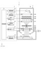
- FIG. 1 shows elements of a drawing apparatus according to a first embodiment.
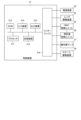
- FIG. 2 shows the hardware configuration of the control device of the first embodiment.
- FIG. 3 shows the structure of the shaped aperture array plate of the first embodiment along the xy plane.
- FIG. 4 shows the structure of the blanking aperture array mechanism of the first embodiment along the xz plane.
- FIG. 5 shows the structure of the blanking aperture array mechanism of the first embodiment along the xy plane.
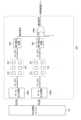
- FIG. 6 shows the circuitry and associated elements of the blanking aperture array arrangement of the first embodiment.
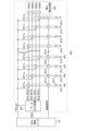
- FIG. 7 shows some elements and connections of the control circuit of the first embodiment and related elements.
- FIG. 8 shows a portion of FIG.
- FIG. 9 schematically shows the transfer and generation of data in the rendering device of the first embodiment.
- FIG. 10 shows some elements and connections of the control circuit of the second embodiment and related elements.
- FIG. 11 schematically shows the transfer and generation of data in the drawing apparatus of the second embodiment.
- each functional block can be implemented as hardware, computer software, or a combination of both. It is not essential that each functional block is distinguished as in the example below. For example, some functions may be performed by functional blocks other than those illustrated. Moreover, the illustrated functional blocks may be divided into finer functional sub-blocks.
- FIG. 1 shows the elements (configuration) of a drawing apparatus according to the first embodiment.
- the drawing device 1 is, for example, a multi-charged particle beam drawing device. Some elements are described in more detail later.
- the drawing device 1 includes a control circuit system 2 and a drawing mechanism 3 .
- the drawing mechanism 3 draws a pattern on the sample 6 by generating a charged particle beam and irradiating the sample 6 with the generated charged particle beam. Examples of the sample 6 include a mask or reticle coated with resist.
- a control circuit system 2 controls the operation of the drawing mechanism 3 .
- the drawing mechanism 3 includes a vacuum chamber 31 .
- the inside of the vacuum chamber 31 is kept in a vacuum, for example, while the drawing device 1 is drawing on the sample 6 .
- the vacuum chamber 31 is composed of a lighting chamber 31a and a lens barrel 31b.
- the lighting chamber 31a has a rectangular parallelepiped shape, for example, and has a space inside.
- a writing chamber 31a accommodates the sample 6 .
- the lighting chamber 31a has an opening on its upper surface and is connected to the internal space of the lens barrel 31b at the opening.
- the drawing device 1 also includes a stage 310 within the writing chamber 31a.
- a sample 6 is placed on the upper surface of the stage 310 during writing.
- the stage 310 can move along the x-axis and the y-axis while holding the sample 6 substantially horizontally.
- a mirror 312 x and a mirror 312 y are provided on the upper surface of the stage 310 .
- Mirror 312x extends along the y-axis and mirror 312y extends along the x-axis.
- Mirrors 312 x and 312 y are used as references for detection of the position of stage 310 .
- the lens barrel 31b has a cylindrical shape extending along the z-axis and is made of stainless steel, for example.
- the lower end of the lens barrel 31b is positioned inside the lighting chamber 31a.
- the drawing apparatus 1 includes an electron gun 320, an illumination lens 330, a reduction lens 331, an objective lens 332, a shaping aperture array plate 340, a limiting aperture array plate 341, a blanking aperture array mechanism (blanking aperture array system (blanking aperture array substrate) 350 and deflectors 360 and 361 .
- the electron gun 320 is located at the top inside the lens barrel 31b.
- the electron gun 320 is, for example, a hot cathode electron gun, and includes elements such as a cathode, a Wehnelt electrode, and an anode.
- the electron gun 320 receives the voltage, it emits an electron beam EB downward along the z-axis (-z direction).
- the electron beam EB spreads along the xy plane as it travels along the z axis.
- the illumination lens 330 is an annular electromagnetic lens and is positioned below the electron gun 320 along the z-axis.
- the illumination lens 330 shapes the electron beam EB, which has reached the illumination lens 330 and spreads in the xy plane, so that it travels in parallel along the z-axis.
- the shaping aperture array plate 340 is located below the illumination lens 330 along the z-axis.
- the shaping aperture array plate 340 has a plurality of apertures, and allows a portion of the electron beam EB incident on the shaping aperture array plate 340 to pass through the plurality of apertures and split into a plurality of electron beams EBm.
- the blanking aperture array mechanism 350 is located below the shaping aperture array plate 340 along the z-axis (-z direction).
- a blanking aperture array mechanism 350 individually blanks a plurality of electron beams EBm.
- the blanking aperture array mechanism 350 has a plurality of apertures, each positioned below ( ⁇ z direction) along the z-axis of the opening of the shaping aperture array plate 340, and blankers provided around each aperture. Each blanker blanks the electron beam EBm incident on the target aperture provided with the blanker.
- the reduction lens 331 is an annular electromagnetic lens and is positioned below the blanking aperture array mechanism 350 along the z-axis (-z direction). The reduction lens 331 focuses the parallel electron beams EBm that have passed through the blanking aperture array mechanism 350 to the center of the aperture of the limiting aperture array plate 341 .
- the limiting aperture array plate 341 has a plate-like shape extending along the xy plane and has an aperture in the center of the xy plane.
- the aperture is located near the convergence point (crossover point) of the multiple electron beams EBm that have passed through the reduction lens 331 .
- the beam deflected by the blanker provided in the blanking aperture array mechanism 350 cannot pass through the aperture provided in the center of this limiting aperture array plate 341, hits the limiting aperture array plate 341, and is blanked. be done.
- the limiting aperture array plate 341 shapes the shape of the electron beams EBm along the xy plane by allowing the plurality of electron beams EBm to pass through the apertures.
- a plurality of shaped electron beams EBm form shots of a certain shape.
- the deflector 360 is located below the limiting aperture array plate 341 along the z-axis (-z direction). A shot-shaped electron beam EBm emitted from the limiting aperture array plate 341 is incident on the deflector 360 .
- Deflector 360 includes multiple pairs of electrodes. In FIG. 1 only one pair of electrodes is shown to avoid unnecessary clutter of the drawing. The two electrodes that make up each pair face each other. Each electrode receives a voltage, and deflector 360 deflects the incident electron beam EBm along the x-axis and/or along the y-axis in response to the application of voltages to the multiple electrodes.
- the objective lens 332 is an annular electromagnetic lens and surrounds the deflector 360 .
- the objective lens 332 cooperates with the deflector 360 to focus the electron beam EBm to a specific position on the specimen 6.
- the deflector 361 is located below the deflector 360 along the z-axis (-z direction).
- the electron beam EBm that has passed through the deflector 360 is incident on the deflector 361 .
- Deflector 360 includes multiple pairs of electrodes. In FIG. 1 only one pair of electrodes is shown to avoid unnecessary clutter of the drawing. The two electrodes that make up each pair face each other. Each electrode receives a voltage, and deflector 360 deflects the incident electron beam EBm along the x-axis and/or along the y-axis in response to the application of voltages to the multiple electrodes.
- the control circuit system 2 includes a control device 21 , a power supply device 22 , a lens drive device 23 , a BAA control unit 24 , a dose control unit 25 , a deflector amplifier 27 and a stage drive device 28 .
- the control device 21 controls the power supply device 22 , the lens driving device 23 , the BAA control unit 24 , the irradiation amount control unit 25 , the deflector amplifier 27 and the stage driving device 28 .
- the control device 21 receives input from the user of the drawing apparatus 1, and based on the received input, the power supply device 22, the lens driving device 23, the BAA control unit 24, the dose control unit 25, and the deflector amplifier 27. , and the stage drive 28 .
- the power supply device 22 receives control data from the control device 21 and applies voltage to the electron gun 320 based on the received control data.
- the lens drive device 23 receives control data from the control device 21 and controls the illumination lens 330 based on the received control data. Specifically, the lens driving device 23 controls the strength of the illumination lens 330 with respect to the electron beam EB, that is, the strength with which the electron beam EB is refracted. The lens driving device 23 adjusts the intensity of the illumination lens 330 by converting the electron beam EB, which enters the illumination lens 330 from above the z-axis of the illumination lens 330 and spreads along the xy plane as it travels, into an electron beam substantially parallel to the z-axis. Control to shape to line.
- the lens driving device 23 also receives control data from the control device 21 and controls the strength of the reduction lens 331 based on the received control data.
- the lens driving device 23 adjusts the intensity of the reduction lens 331 so that the electron beam EBm incident on the reduction lens 331 from above the reduction lens 331 on the z-axis without being deflected by blanking by the blanker of the blanking aperture array mechanism 350 is controlled by the limiting aperture. It is controlled so as to focus on the center of the aperture of the array plate 341 .
- the lens driving device 23 further receives control data from the control device 21 and controls the strength of the objective lens 332 based on the received control data.
- the lens driving device 23 controls the intensity of the objective lens 332 so that the electron beam BM incident on the objective lens 332 from above the z-axis of the objective lens 332 is focused on the upper surface of the sample 6 . Note that the lens driving device 23 may reduce the electron beam BM.
- the BAA control unit 24 receives BAA control data from the control device 21 and controls the blanking aperture array mechanism 350 based on the received control data.
- the dose control unit 25 receives control data from the control device 21 and generates dose control data based on the received control data.
- the dose control unit 25 supplies the generated dose control data to the BAA control unit 24 to control the dose of the electron beam BM to the sample 6 via the BAA control unit 24 .
- the deflector amplifier 27 receives control data from the control device 21 and generates control signals for controlling the deflectors 360 and 361 based on the received control data.
- the generated control signals are supplied to deflectors 360 and 361, respectively.
- the signal for deflector 360 specifies the potential difference between the two electrodes of each pair of deflector 360 .
- the signal for deflector 361 specifies the potential difference between the two electrodes of each pair of deflector 361 .
- Deflector amplifier 27 generates a signal for deflector 360 such that deflector 360 receives a voltage that deflects electron beam EBm by an amount and/or direction specified by controller 21 .
- deflector amplifier 27 generates a signal for deflector 361 such that deflector 361 receives a voltage that deflects electron beam EBm by an amount and/or direction specified by controller 21 . .
- the stage driving device 28 measures the positions of the mirrors 312x and 312y using means such as a laser sensor (not shown), and detects the position of the stage 310 based on the measured positions.
- the stage drive device 28 also receives control data from the control device 21 and drives the stage 310 based on the received control data. By driving the stage 310, the sample 6 is moved to a desired position.
- FIG. 2 shows the configuration of the control device 21 of the first embodiment, and particularly shows the hardware configuration.
- the controller 21 includes a processor 211 , a ROM (read only memory) 212 , a storage device 213 , an input device 214 , an output device 215 and an interface 216 .
- ROM read only memory
- the ROM 212 nonvolatilely stores a program for controlling the processor.
- Storage device 213 includes volatile memory, non-volatile memory, and/or hard disk and retains data.
- the processor 211 is, for example, a CPU (central processing unit) and is stored in the ROM 212 and performs various operations by executing programs loaded in the storage device 213 .
- Processor 211 controls storage device 213, input device 214, output device 215, and interface 216 according to a program.
- the program is configured to allow the controller 21, particularly the processor 211, to perform various operations.
- the input device 214 includes one or more of a keyboard, mouse, and touch panel, and allows the user of the rendering device 1 to input instructions and/or parameters.
- the output device 215 includes a display and presents various information to the user of the rendering device 1 .
- the interface 216 controls communication by the control device 21 with the power supply device 22 , the lens driving device 23 , the BAA control unit 24 , the irradiation amount control unit 25 , the deflector amplifier 27 and the stage driving device 28 .
- FIG. 3 schematically shows the structure of the shaping aperture array plate 340 of the first embodiment along the xy plane.
- shaping aperture array plate 340 extends along the xy plane and has, for example, a rectangular shape.
- the shaped aperture array plate 340 has, for example, silicon as a base, and the surface of the base is covered with a thin film.
- the thin film is, for example, chromium and can be formed by plating or sputtering.
- the shaping aperture array plate 340 has a plurality of apertures 340a.
- Apertures 340a pierce through two opposing surfaces along the z-axis of shaping aperture array plate 340, namely, a top surface and a bottom surface.
- Apertures 340a are arranged, for example, in a matrix along the x-axis and the y-axis.
- Apertures 340a are, for example, square and have substantially the same shape as each other.
- the electron beam EB emitted from the electron gun 320 is shaped by the illumination lens 330 so as to be parallel along the z-axis, and is incident on the upper surface of the shaping aperture array plate 340 . Part of the incident electron beam EB is blocked by the shaping aperture array plate 340 and the rest passes through the aperture 340a.
- Such selective shielding and passage of the electron beam EB divides (multiplies) the electron beam EB into a plurality of electron beams EBm traveling downward along the z-axis.
- FIG. 4 shows the structure of the blanking aperture array mechanism 350 of the first embodiment along the xz plane.
- blanking aperture array mechanism 350 includes base 351 .
- the base 351 extends along the xy plane.
- a substrate 352 is provided on the upper surface of the base 351 .
- the substrate 352 is made of, for example, a semiconductor such as silicon.
- the substrate 352 rests on the top surface of the substrate 352 at the bottom edge and is thinner than the edge at the central portion 352a.
- Substrate 352 also includes a plurality of apertures 353 in central portion 352a. Each aperture 353 spans the top and bottom surfaces of substrate 352 .
- Apertures 353 are arranged in the xy plane. Each aperture 353 is positioned below the apertures 340a of the shaping aperture array plate 340 along the z-axis, and has a shape in the xy plane similar to, for example, the shape of the apertures 340a in the xy plane.
- each aperture 353 substantially coincides with the center of the aperture 340a of the shaping aperture array plate 340 on the xy plane.
- the aperture 353 allows the electron beam EBm that has passed through the aperture 340a of the shaping aperture array plate 340 to pass therethrough.
- the blanking aperture array mechanism 350 also includes multiple electrode pairs 354 .
- Each electrode pair 354 is provided for one aperture 340a and includes electrodes 355 and 356 and functions as a blanker.
- Electrodes 355 and 356 include or consist of copper, for example. Electrodes 355 and 356 of each electrode pair 354 are spaced apart from each other and sandwich one aperture 353 against which the electrode pair 354 is provided.
- a control circuit 357 is provided in a portion of the substrate 352 between the adjacent electrode pairs 354 (between the electrode 355 of one electrode pair 354 and the electrode 356 of the adjacent electrode pair 354). Each control circuit 357 is provided for one electrode pair 354 . Each control circuit 357 receives various control signals and, based on the received control signals, applies a voltage to one electrode pair 354 for which the control circuit 357 is provided. Each control circuit 357 includes elements such as a plurality of transistors and resistors formed on the substrate 352 .
- a data output circuit 359 is provided at the end of the central portion 352 a of the substrate 352 .
- Each data output circuit 359 receives control data DLS from the BAA control unit 24, and outputs control data DL in a format different from the control data DLS in parallel from the received control data DLS.
- the data output circuit 359 includes elements such as a plurality of transistors and resistors formed on the substrate 352 .
- FIG. 5 shows the structure of the blanking aperture array mechanism 350 of the first embodiment along the xy plane.
- each electrode 356 has a rectangular shape with one side removed.
- the three sides of electrode 356 extend along the three sides of aperture 353 surrounded by electrode 356 .
- FIG. 5 shows, by way of example, a structure in which each electrode 356 is along two sides of the aperture 353 parallel to the x-axis and the left side of the two sides parallel to the y-axis.
- Each electrode 355 extends along a side of the corresponding aperture 353 along which the electrode 355 and the electrode 356 forming the electrode pair 354 do not extend.
- FIG. 5 shows a structure in which each electrode 355 is along the right side of the two sides parallel to the y-axis.
- the electrode 356 is grounded. Each electrode 355 is electrically connected to one control circuit 357 corresponding to that electrode 355 .
- Each control circuit 357 receives various control signals as described above.
- the control signals include clock signals and control data DL.
- Control signals are provided by the BAA control unit 24 .
- Control circuit 357 is also connected to a node of internal power supply potential VCC (eg, 5V).
- VCC internal power supply potential
- Each electrode 356 is connected to a node of common (ground) potential VSS (eg, 0V).
- VSS common (ground) potential
- FIG. 6 is a circuit diagram of the blanking aperture array mechanism 350 of the first embodiment, showing further relevant elements.
- the blanking aperture array arrangement 350 has a plurality of data output circuits 359 (359A, 359B, . . . ).
- Each data output circuit 359 receives a clock from the BAA control unit 24 and also receives control data DLS (DLSA, DLSB, . . . ) for that data output circuit 359 . That is, data output circuit 359A receives control data DLSA from BAA control unit 24, and data output circuit 359B receives control data DLSB from BAA control unit 24.
- FIG. Other data output circuits 359 are similar.
- the control data DLS consists of a plurality of bits.
- Each data output circuit 359 is connected to a set of control circuits 357 . Each data output circuit 359 outputs a plurality of control data DL in parallel based on the received control data DLS. Each data output circuit 359 also outputs an error detection code EDT for certain control data DL. Although the error detection code EDT is generated by the data output circuit 359 in this embodiment, it may be generated by the BAA control unit 24 . The error detection code EDT output by the data output circuit 359 is received by the error detection circuit 358 connected to the data output circuit 359 via the control circuit 357 . This received error detection code EDT is hereinafter referred to as the transmitted error detection code EDT.
- Blanking aperture array mechanism 350 further includes as many error detection circuits 358 and logical sum (OR) gates 3582 as there are data output circuits 359 included in blanking aperture array mechanism 350 .
- Each control circuit 357 includes a register, as described below, and sets of control circuits 357 can transfer data through the registers. Details of the control circuit 357 will be described later.
- Each error detection circuit 358 is provided for a set of control circuits 357 and is connected to a plurality of control circuits 357 of the set of control circuits 357 .
- the details of the connection between the error detection circuit 358 and the corresponding set of control circuits 357 will be described later.
- Each error detection circuit 358 receives control data DL from a plurality of control circuits 357 connected to that error detection circuit 358 .
- Each error detection circuit 358 receives certain control data DL and transmission error detection code EDT for the control data DL from the data output circuit 359 via the control circuit 357 .
- Each error detection circuit 358 detects an error in the received control data DL based on the received control data DL and the transmission error detection code EDT. Specifically, it is as follows.
- Each error detection circuit 358 generates an error detection code by a certain method from the received data, that is, the control data DL.
- the techniques that may be used can be of any type, examples of techniques include CRC (cyclic redundancy check) and checksums.
- the error-detecting code generated by the error-detecting circuit 358 is hereinafter referred to as a calculated error-detecting code EDC.
- the transmission error detection code EDT and the calculated error detection code EDC for certain control data DL should match if the control data DL is correctly transmitted from the data output circuit 359 to the error detection circuit 358. . Based on this fact, the error detection circuit 358 compares the transmitted error detection code EDT with the calculated error detection code EDC.
- the error detection circuit 358 When the transmission error detection code EDT for certain control data DL and the calculated error detection code EDC do not match, the error detection circuit 358 outputs a detection signal indicating that they do not match.
- This detection signal is, for example, a digital signal and indicates detection of a mismatch by a high level.
- An OR gate 3582 receives detection signals from all error detection circuits 358 .
- OR gate 3582 outputs a high-level annunciation signal indicating error detection when any one of the received detection signals has a high level.
- the notification signal output by OR gate 3582 is transmitted to control device 21 .
- the control device 21 receives the notification signal indicating the error detection, it notifies the user of the error detection by using the output device 215 in FIG. 2, for example.
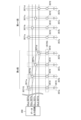
- FIG. 7 is a more detailed circuit diagram of part of the blanking aperture array mechanism 350 of the first embodiment, and representatively shows elements directly or indirectly connected to one data output circuit 359 .
- the portion connected to other data output circuits 359 also has the elements and connections shown in FIG.
- FIG. 7 shows an example of four control data DL.
- the four control data DL are called control data DLa, DLb, DLc and DLd.
- Each control circuit 357 receives control data DLa, DLb, DLc, or DLd.
- the transmission error correction codes EDT for the control data DLa, DLb, DLc, and DLd are sometimes referred to as transmission error correction codes EDTa, EDTb, EDTc, and EDTd, respectively.
- Control circuits 357 that receive control data DLa, DLb, DLc, and DLd, respectively, may be referred to as control circuits 357a, 357b, 357c, and 357d.
- Each control circuit 357 includes one register (eg, D-type flip-flop) 3571 (3571a, 3571b, 3571c, 3571d), at least one buffer 3572, and a level shifter 3573.
- FIG. 7 and the following description are based on the example that each control circuit 357 includes one buffer 3572 .
- Each register 3571 and each buffer 3572 hold 1-bit data.
- the output of register 3571 is connected to the input of buffer 3572 .
- Each buffer 3572 receives a control signal from, for example, the BAA control unit 24, holds data received at its input based on the control signal, and outputs the data it holds based on the control signal.
- Each control circuit 357 may include multiple buffers 3572 connected in series.
- each control circuit 357 the output of the buffer 3572 is connected to the input of the level shifter 3573.
- the level shifter 3573 converts the voltage level of the received input and outputs a voltage corresponding to the input.
- the output voltage is applied to one electrode 355 controlled by a control circuit 357 that outputs the voltage.
- Application of a voltage to each electrode 355 creates a potential difference between that electrode 355 and its counterpart electrode 356, as described above. This potential difference bends the trajectory of the electron beam EBm entering the region between the electrodes 355 and 356, blanking the electron beam EBm.
- a register 3571 receives, for example, a clock as a control signal from the BAA control unit 24 .
- Register 3571 is connected to data output circuit 359 by a signal line.
- the register 3571 receives the control data DL and the transmission error correction code EDT for the control data DL from the data output circuit 359 on the signal line.
- the register 3571 retains the control data DL and the transmission error correction code EDT input from the data output circuit 359 based on the control signal, and also stores the retained control data DL and the transmission error correction code EDT based on the control signal.
- Code EDT is output to buffer 3572 .
- register 3571 of the control circuit 357a is referred to as register 3571a.
- register 3571 of control circuit 357b, register 3571 of control circuit 357c, and register 3571 of control circuit 357d are referred to as registers 3571b, 3571c, and 3571d, respectively.
- Each register 3571a is connected in series with the adjacent register 3571a by a signal line, and the serially connected registers 3571 form a shift register. That is, the output of one register 3571a is directly connected to the input of another register 3571a.
- the registers 3571b are connected in series to form a shift register
- the registers 3571c are connected in series to form a shift register
- the registers 3571c are connected in series to form a shift register.
- the error detection circuit 358 includes the same number of registers 3580 as the number of control data DL, ie registers 3580a, 3580b, 3580c and 3580d in the present example.
- Register 3580a receives the output of register 3571a at the final stage of serially connected registers 3571a.
- registers 3580b, 3580c, and 3580d are, respectively, the output of last stage register 3571b of series-connected register 3571b, the output of last stage register 3571c of series-connected register 3571c, and the output of series-connected register 3571c.
- Error detection circuit 358 calculates a calculated error detection code EDC for the data held in register 3580 .
- FIG. 8 shows part of FIG.
- the n-th (n is a natural number) stage register 3571a, n-th stage register 3571b, n-th stage register 3571c, and n-th stage register 3571d are controls for blanking control of a certain plurality of electron beams EBm.
- Such control data DL are, for example, data for controlling blanking in one operation of any kind.
- 3571a, 3571b, 3571c, and 3571d in one such stage receive control data DLa, DLb, DLc, and DLd that make up some control data DL, and so on registers 3571a, 3571a, 3571b, 3571c, and 3571d are hereinafter referred to as register set 3571G.
- Buffer set 3572G consists of a total of four buffers 3572 in each of four control circuits 357 each containing four registers 3571 of register set 3571G in one stage.
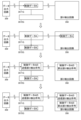
- FIG. 9 schematically shows the transfer and generation of data in the rendering device 1 of the first embodiment.
- FIG. 9 shows data in a register set 3571G, a buffer set 3572G connected to this register set 3571G, and error detection circuit 358.
- FIG. 9 shows data in a register set 3571G, a buffer set 3572G connected to this register set 3571G, and error detection circuit 358.
- the data output circuit 359 outputs the control data A as shown in the uppermost portion of FIG.
- the control data A is control data DL consisting of a certain bit string, and consists of control data DLa, DLb, DLc, and DLd of certain bit values, for blanking control of a certain plurality of electron beams EBm. It consists of multiple bits that are related to each other.
- control data A is data for controlling blanking in one operation of any kind.
- Output control data A is received by a stage of register set 3571G via register 3571 .
- control data A is transferred to the buffer set 3572G included in the control circuit 357 including the register set 3571G that received the control data A.
- control data DLa of the control data A is transferred to the buffer 3572 in the control circuit 357 including the nth stage register 3571a.
- data received as control data DLb of control data A is transferred to buffer 3572 in control circuit 357 including n-th stage register 3571b.
- Data received as control data DLc of control data A is transferred to buffer 3572 in control circuit 357 including n-th stage register 3571c.
- Data received as control data DLd of control data A is transferred to buffer 3572 in control circuit 357 including n-th stage register 3571d.
- Control data A is then transferred from buffer set 3572G to a set of level shifters 3573 (not shown).
- control data A is transferred to the error detection circuit 358 via the register 3571 in the stage after the stage of the register set 3571G. That is, the data received as the control data DLa of the control data A reaches the register 3580a of the error detection circuit 358 from the nth stage register 3571a via the (n+1)th stage and subsequent registers 3571a. do. The data received as the control data DLb of the control data A reaches the register 3580b of the error detection circuit 358 from the nth stage register 3571b via the (n+1)th stage and subsequent registers 3571b.
- the data received as the control data DLc of the control data A reaches the register 3580c of the error detection circuit 358 from the n-th stage register 3571c via the (n+1)-th stage and subsequent registers 3571c.
- the data received as the control data DLd of the control data A reaches the register 3580d of the error detection circuit 358 from the nth stage register 3571d via the (n+1)th stage and subsequent registers 3571d.
- the error detection circuit 358 calculates an error detection code (calculated error detection code EDC) for the control data A.
- the data output circuit 359 also calculates an error detection code (transmission error detection code EDT) for the control data A and outputs the transmission error detection code EDT for the control data A.
- the transmission error detection code EDT for the control data A consists of transmission error detection codes EDTa, EDTb, EDTc, and EDTd for the control data DLa, DLb, DLc, and DLd forming the control data DLA, respectively.
- a transmit error detection code EDT for control data A is received by register set 3571G.
- the transmission error detection code EDT for control data A is not transferred to buffer set 3572G unlike control data DL (for example, control data A).
- BAA control unit 24 does not provide the control signal described with reference to FIG. .
- the transmission error detection code EDT for the control data A is passed through the register 3571 in the stage after the stage of the register set 3571G in the same way as the control data DL. Received by circuit 358 .
- FIG. 9 shows an example in which the transmission error detection code EDT for control data A is output from the data output circuit 359 immediately after the control data A.
- the timing at which the transmission error detection code EDT is output is not limited to the example in FIG.
- transmission error detection code EDT for control data A may be output prior to control data A.
- another control data and/or another transmission error detection code EDT may be output between the control data A and the transmission error detection code EDT for the control data A.
- the blanking aperture array mechanism 350 includes an error detection circuit 358, which receives control data DL supplied to the level shifter 3573, calculates a calculated error detection code EDC from the received control data DL, and A transmission error detecting code EDT for the data DL is received, and the calculated error detecting code EDC and the transmission error detecting code EDT are compared.
- the transmission error detection code EDT and the calculated error detection code EDC for certain control data DL should match if the control data DL is correctly transmitted from the data output circuit 359 to the error detection circuit 358 . Therefore, the coincidence between the calculated error detecting code EDC and the transmission error detecting code EDT indicates that the serially connected register 3571 is normal. Therefore, by comparing the calculated error detection code EDC and the transmission error detection code EDT, it is possible to confirm that all the registers 3571 that receive the control data DL output from the data output circuit 359 are normal.
- the transfer of data necessary for such checking includes only the transfer of the transmission error detection code EDT in addition to the transfer of the control data DL in the serially connected registers 3571 in the case where the first embodiment is not applied. . That is, the transmission error detection code EDT can be transferred only by inserting it into the transfer of the control data DL.
- the transmission error detection code EDT consists of only a few bits. Therefore, the transfer of the control data DL and, by extension, the drawing are prevented from being greatly hindered due to the data inspection. In other words, it is possible to inspect the path for transferring the control data DL during drawing without significantly hindering the progress of drawing in cases where the first embodiment is not applied.
- the second embodiment differs from the first embodiment in the configuration of the blanking aperture array mechanism 350 and points related thereto.
- the second embodiment is the same as the first embodiment in other respects. In the following, among the configuration and operation of the second embodiment, points that differ from those of the first embodiment will be mainly described.
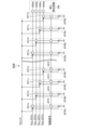
- FIG. 10 is a more detailed circuit diagram of the blanking aperture array mechanism 350 of the second embodiment, and representatively shows elements directly or indirectly connected to one data output circuit 359 .
- the blanking aperture array mechanism 350 of the second embodiment may be referred to as a blanking aperture array mechanism 350B to distinguish it from the blanking aperture array mechanism 350 of the first embodiment.
- the blanking aperture array mechanism 350B differs from the blanking aperture array mechanism 350 of the first embodiment in the details of the control circuit 357.
- the control circuit 357 of the second embodiment may be referred to as a control circuit 357B to distinguish it from the control circuit 357 of the first embodiment.
- a buffer 3572 is further connected at its output to the input of a register 3571 in that control circuit 357B.
- the output of the final stage buffer 3572 is connected to a register 3571 .
- the description so far relates to an example where in every control circuit 357B the output of the buffer 3572 is further connected to the input of the register 3571 in that control circuit 357B.
- Embodiments are not limited to this configuration, and in only one or more of all control circuits 357B, the output of buffer 3572 may be further connected to the input of register 3571 in that control circuit 357B.
- FIG. 11 schematically shows the transfer and generation of data in the rendering device 1 of the second embodiment.
- FIG. 11 shows data in a register set 3571G, a buffer set 3572G connected to this register set 3571G, and error detection circuit 358.
- FIG. 11 shows data in a register set 3571G, a buffer set 3572G connected to this register set 3571G, and error detection circuit 358.
- control data A is received by register set 3571G and transferred to buffer set 3572G.
- control data B is received by register set 3571G and control data A is transferred to buffer set 3572G.
- control data A is transferred to a set of level shifters 3573 (not shown) and transferred again to the register set 3571G.
- control data B is transferred to buffer set 3572G.
- control data A in register set 3571G are stored in stages after the stage of register set 3571G, as described with reference to FIG. 9 of the first embodiment. is transferred to the error detection circuit 358 via the register 3571 of .
- control data A undergoes the same processing as the processing described with reference to the third and bottom rows from the top of FIG. 9 of the first embodiment. That is, the calculated error detection code EDC for the control data A is calculated by the error detection circuit 358, and the transmission error detection code EDT for the control data A is output from the data output circuit 359 via the register 3571 to the error detection circuit. 358.
- the error detection circuit 358 compares the calculated error detection code EDC and the transmission error detection code EDT for the control data A obtained in this way.
- the error detection circuit 358 compares the calculated error detection code EDC and the transmitted error detection code EDT. Therefore, the same advantages as in the first embodiment can be obtained.
- each control circuit 357B includes a register 3571 connected to the output of the buffer 3572 of that control circuit 357B, and the error detection circuit 358 calculates an error detection code from the control data DL received from the buffer 3572 via the register 3571. Calculate the EDC.
- the control data DL in a register 3571 should match the form received by that register 3571 if it was correctly transferred to the buffer 3572 . Therefore, the fact that the calculated error detecting code EDC and the transmission error detecting code EDT that are generated as in the second embodiment match means that the serially connected register 3571 and the buffer 3572 are normal. indicate.
- Blanking aperture array mechanisms 350 and 350B may be used in an inspection system.
Landscapes
- Chemical & Material Sciences (AREA)
- Analytical Chemistry (AREA)
- Physics & Mathematics (AREA)
- General Physics & Mathematics (AREA)
- Electron Beam Exposure (AREA)
Priority Applications (2)
| Application Number | Priority Date | Filing Date | Title |
|---|---|---|---|
| KR1020247016791A KR102918315B1 (ko) | 2021-11-22 | 2022-09-08 | 블랭킹 애퍼처 어레이 시스템 및 하전 입자 빔 묘화 장치 |
| US18/635,723 US20240282550A1 (en) | 2021-11-22 | 2024-04-15 | Blanking aperture array system and charged particle beam writing apparatus |
Applications Claiming Priority (2)
| Application Number | Priority Date | Filing Date | Title |
|---|---|---|---|
| JP2021-189582 | 2021-11-22 | ||
| JP2021189582A JP7604355B2 (ja) | 2021-11-22 | 2021-11-22 | ブランキングアパーチャアレイシステム及び荷電粒子ビーム描画装置 |
Related Child Applications (1)
| Application Number | Title | Priority Date | Filing Date |
|---|---|---|---|
| US18/635,723 Continuation US20240282550A1 (en) | 2021-11-22 | 2024-04-15 | Blanking aperture array system and charged particle beam writing apparatus |
Publications (1)
| Publication Number | Publication Date |
|---|---|
| WO2023089923A1 true WO2023089923A1 (ja) | 2023-05-25 |
Family
ID=86396769
Family Applications (1)
| Application Number | Title | Priority Date | Filing Date |
|---|---|---|---|
| PCT/JP2022/033750 Ceased WO2023089923A1 (ja) | 2021-11-22 | 2022-09-08 | ブランキングアパーチャアレイシステム及び荷電粒子ビーム描画装置 |
Country Status (5)
| Country | Link |
|---|---|
| US (1) | US20240282550A1 (cg-RX-API-DMAC7.html) |
| JP (1) | JP7604355B2 (cg-RX-API-DMAC7.html) |
| KR (1) | KR102918315B1 (cg-RX-API-DMAC7.html) |
| TW (1) | TWI835342B (cg-RX-API-DMAC7.html) |
| WO (1) | WO2023089923A1 (cg-RX-API-DMAC7.html) |
Families Citing this family (1)
| Publication number | Priority date | Publication date | Assignee | Title |
|---|---|---|---|---|
| CN118859638B (zh) * | 2023-11-28 | 2025-09-05 | 上海集成电路材料研究院有限公司 | 一种电子束直写装置 |
Citations (3)
| Publication number | Priority date | Publication date | Assignee | Title |
|---|---|---|---|---|
| JP2014039011A (ja) * | 2012-07-17 | 2014-02-27 | Canon Inc | 描画装置、送信装置、受信装置、および物品の製造方法 |
| JP2015228471A (ja) * | 2014-06-03 | 2015-12-17 | 株式会社ニューフレアテクノロジー | マルチ荷電粒子ビーム描画方法及びマルチ荷電粒子ビーム描画装置 |
| JP2017152485A (ja) * | 2016-02-23 | 2017-08-31 | 株式会社ニューフレアテクノロジー | 診断方法、荷電粒子ビーム描画装置、及びプログラム |
Family Cites Families (8)
| Publication number | Priority date | Publication date | Assignee | Title |
|---|---|---|---|---|
| US4698814A (en) * | 1984-02-06 | 1987-10-06 | U.S. Philips Corporation | Arrangement for checking the parity of parity-bits containing bit groups |
| JP3544759B2 (ja) * | 1995-09-07 | 2004-07-21 | 富士通株式会社 | マルチ荷電粒子ビーム露光方法 |
| WO2001035165A1 (en) | 1999-11-07 | 2001-05-17 | Ion Diagnostics, Inc. | Data path design for multiple electron beam lithography system |
| GB2414111B (en) * | 2004-04-30 | 2010-01-27 | Ims Nanofabrication Gmbh | Advanced pattern definition for particle-beam processing |
| JP6459755B2 (ja) * | 2015-04-28 | 2019-01-30 | 株式会社ニューフレアテクノロジー | マルチ荷電粒子ビーム描画装置及びマルチ荷電粒子ビーム描画方法 |
| JP7189729B2 (ja) * | 2018-10-30 | 2022-12-14 | 株式会社ニューフレアテクノロジー | マルチ荷電粒子ビーム描画装置およびマルチ荷電粒子ビーム描画方法 |
| JP7189794B2 (ja) | 2019-02-12 | 2022-12-14 | 株式会社ニューフレアテクノロジー | マルチ荷電粒子ビーム描画装置及びマルチ荷電粒子ビーム描画方法 |
| JP7458817B2 (ja) | 2020-02-18 | 2024-04-01 | 株式会社ニューフレアテクノロジー | マルチ荷電粒子ビーム描画装置及びマルチ荷電粒子ビーム描画方法 |
-
2021
- 2021-11-22 JP JP2021189582A patent/JP7604355B2/ja active Active
-
2022
- 2022-09-08 WO PCT/JP2022/033750 patent/WO2023089923A1/ja not_active Ceased
- 2022-09-08 KR KR1020247016791A patent/KR102918315B1/ko active Active
- 2022-10-12 TW TW111138652A patent/TWI835342B/zh active
-
2024
- 2024-04-15 US US18/635,723 patent/US20240282550A1/en active Pending
Patent Citations (3)
| Publication number | Priority date | Publication date | Assignee | Title |
|---|---|---|---|---|
| JP2014039011A (ja) * | 2012-07-17 | 2014-02-27 | Canon Inc | 描画装置、送信装置、受信装置、および物品の製造方法 |
| JP2015228471A (ja) * | 2014-06-03 | 2015-12-17 | 株式会社ニューフレアテクノロジー | マルチ荷電粒子ビーム描画方法及びマルチ荷電粒子ビーム描画装置 |
| JP2017152485A (ja) * | 2016-02-23 | 2017-08-31 | 株式会社ニューフレアテクノロジー | 診断方法、荷電粒子ビーム描画装置、及びプログラム |
Also Published As
| Publication number | Publication date |
|---|---|
| TWI835342B (zh) | 2024-03-11 |
| KR102918315B1 (ko) | 2026-01-27 |
| TW202324481A (zh) | 2023-06-16 |
| JP2023076259A (ja) | 2023-06-01 |
| JP7604355B2 (ja) | 2024-12-23 |
| US20240282550A1 (en) | 2024-08-22 |
| KR20240093829A (ko) | 2024-06-24 |
Similar Documents
| Publication | Publication Date | Title |
|---|---|---|
| US9299533B2 (en) | Multi charged particle beam writing apparatus utilizing multiple staged mutually orthogonal beam blankers | |
| US7463173B2 (en) | Charged particle beam apparatus, abnormality detecting method for DA converter unit, charged particle beam writing method, and mask | |
| US9805905B2 (en) | Blanking device for multi-beam of charged particle writing apparatus using multi-beam of charged particle and defective beam blocking method for multi-beam of charged particle | |
| JP7026554B2 (ja) | マルチ荷電粒子ビーム描画装置及びマルチ荷電粒子ビーム描画方法 | |
| US10483088B2 (en) | Multi charged particle beam writing apparatus and multi charged particle beam writing method | |
| US11145489B2 (en) | Multi-charged-particle beam writing apparatus and multi-charged-particle beam writing method | |
| JP7458817B2 (ja) | マルチ荷電粒子ビーム描画装置及びマルチ荷電粒子ビーム描画方法 | |
| US11556061B2 (en) | Multiple charged particle beam writing apparatus and multiple charged particle beam writing method | |
| US9880215B2 (en) | Inspection method for blanking device for blanking multi charged particle beams | |
| US10867774B2 (en) | Multi charged particle beam writing apparatus and multi charged particle beam writing method | |
| US11205557B2 (en) | Multi charged particle beam writing apparatus | |
| US9953800B2 (en) | Multi-charged particle beam writing apparatus and multi-charged particle beam writing method | |
| KR102918315B1 (ko) | 블랭킹 애퍼처 어레이 시스템 및 하전 입자 빔 묘화 장치 | |
| US10283314B2 (en) | Charged particle beam writing apparatus, and charged particle beam writing method | |
| JPH11186144A (ja) | 荷電粒子ビーム露光装置 | |
| US12046447B2 (en) | Multi-charged-particle-beam writing method, multi-charged-particle-beam writing apparatus, and computer-readable recording medium | |
| US11244807B2 (en) | Settling time determination method and multi charged particle beam writing method | |
| US20220319807A1 (en) | Charged particle beam writing apparatus and charged particle beam writing method | |
| US20250037960A1 (en) | Blanking aperture array system, charged particle beam writing apparatus, and method for inspecting blanking aperture array system | |
| JP6732649B2 (ja) | ブランキングアパーチャアレイ装置および荷電粒子ビーム描画装置 | |
| US20260081106A1 (en) | Multi-charged particle beam writing apparatus | |
| US20240395493A1 (en) | Blanking aperture array mechanism and writing apparatus | |
| US20260066222A1 (en) | Multibeam writing method and multibeam writing apparatus | |
| JP2024157192A (ja) | マルチ荷電粒子ビーム描画装置およびマルチ荷電粒子ビーム描画方法 | |
| US20240429022A1 (en) | Multiple charged particle beam writing apparatus and multiple charged particle beam writing method |
Legal Events
| Date | Code | Title | Description |
|---|---|---|---|
| 121 | Ep: the epo has been informed by wipo that ep was designated in this application |
Ref document number: 22895210 Country of ref document: EP Kind code of ref document: A1 |
|
| NENP | Non-entry into the national phase |
Ref country code: DE |
|
| 122 | Ep: pct application non-entry in european phase |
Ref document number: 22895210 Country of ref document: EP Kind code of ref document: A1 |
|
| WWG | Wipo information: grant in national office |
Ref document number: 1020247016791 Country of ref document: KR |