WO2023085348A1 - 水晶素子及び水晶デバイス - Google Patents
水晶素子及び水晶デバイス Download PDFInfo
- Publication number
- WO2023085348A1 WO2023085348A1 PCT/JP2022/041864 JP2022041864W WO2023085348A1 WO 2023085348 A1 WO2023085348 A1 WO 2023085348A1 JP 2022041864 W JP2022041864 W JP 2022041864W WO 2023085348 A1 WO2023085348 A1 WO 2023085348A1
- Authority
- WO
- WIPO (PCT)
- Prior art keywords
- crystal
- less
- thickness
- crystal element
- excitation
- Prior art date
- Legal status (The legal status is an assumption and is not a legal conclusion. Google has not performed a legal analysis and makes no representation as to the accuracy of the status listed.)
- Ceased
Links
Images




Classifications
-
- H—ELECTRICITY
- H03—ELECTRONIC CIRCUITRY
- H03H—IMPEDANCE NETWORKS, e.g. RESONANT CIRCUITS; RESONATORS
- H03H9/00—Networks comprising electromechanical or electro-acoustic elements; Electromechanical resonators
- H03H9/02—Details
- H03H9/125—Driving means, e.g. electrodes, coils
- H03H9/13—Driving means, e.g. electrodes, coils for networks consisting of piezoelectric or electrostrictive materials
- H03H9/132—Driving means, e.g. electrodes, coils for networks consisting of piezoelectric or electrostrictive materials characterized by a particular shape
-
- H—ELECTRICITY
- H03—ELECTRONIC CIRCUITRY
- H03H—IMPEDANCE NETWORKS, e.g. RESONANT CIRCUITS; RESONATORS
- H03H9/00—Networks comprising electromechanical or electro-acoustic elements; Electromechanical resonators
- H03H9/02—Details
- H03H9/125—Driving means, e.g. electrodes, coils
- H03H9/145—Driving means, e.g. electrodes, coils for networks using surface acoustic waves
-
- H—ELECTRICITY
- H03—ELECTRONIC CIRCUITRY
- H03H—IMPEDANCE NETWORKS, e.g. RESONANT CIRCUITS; RESONATORS
- H03H9/00—Networks comprising electromechanical or electro-acoustic elements; Electromechanical resonators
- H03H9/15—Constructional features of resonators consisting of piezoelectric or electrostrictive material
- H03H9/17—Constructional features of resonators consisting of piezoelectric or electrostrictive material having a single resonator
- H03H9/19—Constructional features of resonators consisting of piezoelectric or electrostrictive material having a single resonator consisting of quartz
-
- H—ELECTRICITY
- H03—ELECTRONIC CIRCUITRY
- H03H—IMPEDANCE NETWORKS, e.g. RESONANT CIRCUITS; RESONATORS
- H03H9/00—Networks comprising electromechanical or electro-acoustic elements; Electromechanical resonators
- H03H9/25—Constructional features of resonators using surface acoustic waves
-
- H—ELECTRICITY
- H03—ELECTRONIC CIRCUITRY
- H03H—IMPEDANCE NETWORKS, e.g. RESONANT CIRCUITS; RESONATORS
- H03H9/00—Networks comprising electromechanical or electro-acoustic elements; Electromechanical resonators
- H03H9/15—Constructional features of resonators consisting of piezoelectric or electrostrictive material
- H03H9/17—Constructional features of resonators consisting of piezoelectric or electrostrictive material having a single resonator
Definitions
- the present disclosure relates to crystal elements and crystal devices.
- a crystal element that obtains a signal by resonating a crystal blank at a predetermined frequency has a characteristic (DLD: Drive Level Dependency, excitation level dependency) in which the frequency increases as the excitation level (drive level) increases.
- DLD Drive Level Dependency, excitation level dependency
- Japanese Patent Application Laid-Open No. 2020-25344 discloses a technique for improving the structure and shape of the electrodes in order to improve the DLD characteristics.
- One aspect of the present disclosure is as follows.
- a crystal element comprising A crystal element in which the DLD characteristic of the crystal element includes a positive direction (+) portion and a reverse direction ( ⁇ ) portion.
- [A3] The crystal element according to [A1] or [A2], wherein the crystal element has a resonance frequency of 40 MHz or more and 400 MHz or less.
- [A4] The crystal element according to any one of [A1] to [A3], wherein the conductive layer of the crystal element has a thickness of 50 nm or more and 600 nm or less.
- [A5] The crystal element according to any one of [A1] to [A4], wherein the crystal impedance of the crystal element is less than 30 ⁇ .
- [A6] Any one of [A1] to [A5], wherein the product of the thickness (mm) of the conductive layer and the resonance frequency (MHz) of the crystal element is 0.017272 or more and 0.019684 or less.
- [A7] The crystal element according to any one of [A1] to [A6], wherein the pair of electrodes are at the same position in plan view.
- [A8] A crystal device comprising the crystal element according to any one of [A1] to [A7]. Another aspect of the present disclosure is as follows. [B1] crystal piece; A base layer positioned on both surfaces of the crystal piece at the same position in a plan view, and a conductive layer positioned on the base layer and having a gold content of 90% or more by mass. an electrode having A crystal element comprising The crystal element, wherein the product of the thickness (mm) of the conductive layer and the resonance frequency (MHz) of the crystal element is 0.017272 or more and 0.019684 or less. [B2] The crystal element according to [B1], wherein the value of the product is 0.017933 or more and 0.018363 or less. [B3] The crystal element according to [B1] or [B2], wherein the resonance frequency is 76.8 MHz. [B4] A crystal device comprising the crystal element according to any one of [B1] to [B3].
- FIG. 4 is a chart showing DLD characteristics according to the thickness of excitation electrodes when a target resonance frequency is specified;
- FIG. 4 is a schematic diagram for explaining DLD characteristics;
- FIG. 4 is a graph showing an example of measurement of DLD characteristics according to the thickness of excitation electrodes; It is the figure which expanded a part of FIG. 5A.
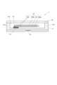
- FIG. 1 is a diagram showing a cross-sectional shape of a crystal device 1 of this embodiment.
- the crystal device 1 includes a base 11, a crystal vibrating element 12 (crystal element), a conductive adhesive 13, a lid 14, parts 15, and the like.
- the substrate 11 is not particularly limited, but is, for example, ceramic material, crystal, semiconductor material, glass material, or a combination thereof.
- the base 11 has a concave portion 11a in the center on the upper surface side.
- An electrode pad 111 protruding from the bottom surface of the recess 11a is positioned.
- the electrode pad 111 has a planar upper surface and can be formed by, for example, screen printing. Also, the uppermost surface of the electrode pad 111 may be plated with gold.
- a crystal vibrating element 12 is adhered to the electrode pad 111 with a conductive adhesive 13 .
- the conductive adhesive 13 may be, for example, a resin-based adhesive containing silver filler (for example, a silicone-based resin or an epoxy resin). In particular, the conductive adhesive 13 made of silicone resin is soft even after being adhered, so it is less likely to adversely affect vibrations.
- the crystal vibrating element 12 has a crystal piece 121, a lower electrode 122a and an upper electrode 122b (collectively excitation electrodes 122; electrodes), a mounting electrode 124, and the like.
- the excitation electrodes 122 are in contact with both surfaces of the crystal blank 121 with the vibrating portion of the crystal blank 121 sandwiched from above and below.
- the mounting electrodes 124 are connected to the electric circuit inside the base 11 via the electrode pads 111 in order to mount the crystal vibrating element 12 on the base 11 and apply a voltage to the excitation electrodes 122 from the outside of the crystal vibrator 12 . It is an electrode and is adhered with a conductive adhesive 13 .
- excitation electrodes 122 and mounting electrodes 124 have a laminated structure of a base layer and a conductive layer positioned on the upper surface side of the base layer.
- the underlayer plays a role of adhering the crystal piece 121 and the conductive layer.
- Such underlayers are for example Cr, Ni, NiCr, Ti or Mo.
- Cr is more preferable because it has a relatively low boiling point and can form an underlayer on the crystal piece 121 at a relatively low temperature.
- the thickness of the underlayer is, for example, 1 nm or more and 20 nm or less, and preferably 10% or less of the thickness of the conductive layer. It is preferable that the thickness of the underlayer is 1 nm or more because, when the crystal resonator 12 is affected by heat, the components of the underlayer diffuse into the conductive layer, thereby suppressing deterioration of adhesion of the conductive layer.
- the thickness of the underlying layer is 20 nm or less, since the deterioration of the electrical properties of the underlying layer with respect to the conductive layer is suppressed.
- the conductive layer is not particularly limited as long as it is made of a metal with high electrical conductivity, but the density ⁇ (g cm ⁇ 3 ) of the conductive layer is preferably 15 or more and 25 or less, particularly preferably 18. 20 or less. More preferably, the conductive layer is gold (Au) here.
- Au gold
- the term "gold” as used herein means that the content of gold is 90% or more (impurities are less than 10%), preferably 95% or more, and particularly preferably 99% or more, by mass. Gold is preferable in that it is chemically more stable than other materials, does not easily react with oxygen and sulfur in the atmosphere, and as a result hardly causes changes in the frequency of the crystal vibrating element.
- the conductive layer may contain Ag, Al, or Cu. Note that the number of conductive layers may be two or more.
- the thickness of the conductive layer is usually 50 nm or more, preferably 75 nm or more, more preferably 100 nm or more, and particularly preferably 200 nm or more. Also, the thickness of the conductive layer is usually 600 nm or less, more preferably 450 nm or less, and particularly preferably 300 nm or less.
- the excitation electrode 122 and mounting electrode 124 having such a base layer and conductive layer may be formed by, for example, physical adsorption at predetermined positions using a sputtering device or a vapor deposition device.
- the crystal piece 121 has a substantially rectangular plate-like shape.
- the crystal piece 121 may be, for example, AT-cut, SC-cut or BT-cut, preferably AT-cut.
- residues may be left on the side surfaces due to the anisotropy of the etching.
- the corners of the crystal piece 121 may be rounded.
- the shape of crystal piece 121 is not particularly limited, but is preferably rectangular.
- the long side of the rectangular crystal piece 121 is usually 300 ⁇ m or more and 1500 ⁇ m or less, preferably 500 ⁇ m or more and 1200 ⁇ m or less, and particularly preferably 700 ⁇ m or more and 1000 ⁇ m or less.
- the short side of the rectangular crystal piece 121 is not particularly limited as long as it is shorter than the long side of the crystal piece 121, but it is usually 100 ⁇ m or more and 1100 ⁇ m or less, preferably 250 ⁇ m or more and 900 ⁇ m or less, and particularly preferably 400 ⁇ m or more and 700 ⁇ m or less. be.
- the ratio of the short side to the long side of the crystal piece 121 is usually 0.07 or more and less than 1, preferably 0.25 or more and 0.9 or less, and particularly preferably 0.5 or more and 0.8 or less.
- the thickness T1 of the crystal piece 121 is defined according to the resonance frequency of the crystal vibrating element 12 . Note that the thickness T1 of the crystal piece 121 is not limited to being uniform throughout. As long as the thickness of the vibrating portion is defined as above, the portion surrounding the vibrating portion may be thicker/thinner, or the portion of the mounting electrode 124 (one end side of the crystal piece 121). Only the thickness may be increased.
- the resonance frequency of the crystal vibrating element 12 is usually 40 MHz or higher, preferably 45 MHz or higher, more preferably 50 MHz or higher, and even more preferably 75.8 MHz or higher.
- the resonance frequency of the crystal resonator 12 is usually 400 MHz or less, preferably 300 MHz or less, more preferably 200 MHz or less, even more preferably 150 MHz or less, particularly preferably 77.8 MHz or less, and particularly preferably 76.8 MHz. .
- the upper surface side of the concave portion 11a of the base 11, that is, the upper end of the frame 112 surrounding the concave portion 11a is joined to the lid 14 via a conductive sealing member such as gold tin or silver solder, thereby forming the concave portion 11a. is sealed.
- a conductive frame-shaped metallized layer may be positioned between the base 11 and the lid 14 .
- the electrode pads 111 can be electrically connected to the outside via signal lines (not shown) penetrating the base 11 (for example, external connection pads located on the bottom surface of the base 11 can be connected to external wiring or the substrate). .
- a component 15 is positioned on the bottom side of the base 11 .
- the component 15 may be an electronic component such as an IC chip, or may be a sensor such as a temperature detecting element (thermistor, etc.). Also, the component 15 may be a combination of a plurality of these. These are for outputting supplementary information relating to the adjustment of the oscillation frequency of the crystal oscillator 12, or performing adjustment according to the supplementary information. TCXO) or the like. Note that the position of the component 15 may not be near the center of the bottom surface in plan view, but may be at a deviated position.
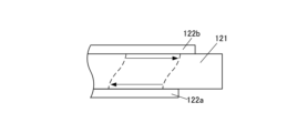
- FIG. 2A to 2C are diagrams for explaining vibration of the crystal vibrating element 12.
- FIG. The crystal blank 121 of the crystal vibrating element 12 is polarized in accordance with the voltage applied between the upper electrode 122b and the lower electrode 122a, and is polarized in a plane perpendicular to the polarization direction, that is, in the extending direction of the crystal blank 121. thickness-shear vibration occurs along the At this time, as shown in FIG. 2A, the excitation electrode 122 is approximately a rigid body, and is simply weights positioned on the upper and lower surfaces of the crystal blank 121, respectively.
- the electrode can no longer be approximated as a rigid body, and each accompanies elastic vibration. That is, an electrode material having a different modulus of elasticity, gold in this case, is arranged in series with the crystal piece 121 .
- the excitation electrode 122 can also vibrate in the same axial direction as the thickness-shear vibration direction of the crystal piece 121 .
- oscillation occurs in which the crystal element 121, the lower electrode 122a, and the upper electrode 122b are connected in series. That is, since the synthesized spring constant kt is obtained by synthesizing the spring constant k1 of the crystal element 121 and the spring constant k2 of the excitation electrode 122, it is expressed by the following equation (1).
- k t k 1 ⁇ k 2 /(k 1 +k 2 ) ... (Formula 1)
- the coefficients i m and j n are values determined by the crystal piece 121 and the excitation electrode 122, respectively. It should be noted that even in non-linear springs, vibrations of very high orders (eg, 4th-7th orders and higher) are usually negligible.
- the actual crystal vibrating element 12 has weight, and in particular, the weight of gold, which is the excitation electrode 122, cannot be ignored. It is Note that the thickness of the base layer of the excitation electrode 122 is sufficiently smaller (less than 10%) than the thickness of the conductive layer as described above, and its weight is also sufficiently small considering the density ratio. can be neglected.
- the contact area S between the crystal piece 121 and the excitation electrode 122 is roughly defined by the resonance frequency F. Therefore, with a certain material (that is, with a single density ⁇ ), the mass M is mainly excited It depends on the thickness T 2 of the electrode 122 .
- the thickness T2 of the excitation electrode 122 is the average thickness of the conductive layer thickness of the lower electrode 122a and the conductive layer thickness of the upper electrode 122b.
- the force (excitation level) that excites the vibration of the crystal oscillator 12 is determined here by the average value ⁇ P> of the power P applied to the crystal oscillator 12 .
- the displacement velocity v1 and the displacement acceleration a1 which are differential values of the amplitude u1 , depend on the resonance frequency F of the amplitude u1 in addition to the excitation level.
- the displacement of the excitation electrode 122 is of course the same as the displacement of the crystal blank 121 at the contact surface between the excitation electrode 122 and the crystal blank 121 .
- the rigidity and inertia of the excitation electrode 122 mass of gold x contact area with the crystal piece 121 x thickness T2 perpendicular to the contact surface with the crystal piece 121) , and the displacement acceleration a 1 ) of the crystal blank 121 , deformation in the sliding direction (in the same axial direction as the deformation direction of the crystal blank 121 ) is considered to occur so that the displacement of the crystal blank 121 is delayed.
- the displacement of the excitation electrode 122 on the side opposite to the side in contact with the crystal blank 121 is the displacement of the crystal blank 121 .
- the displacement acceleration a1 of the surface of the crystal piece 121 the following expression 2 is obtained.
- u 2 T 2 ⁇ a 1 /V 2 (Equation 2)
- V2 is a constant that depends on the rigidity and mass, that is, based on the material of the excitation electrode 122, and is the sound velocity of thickness slip in the material.
- the amplitude u2 thus depends on the excitation level and the resonant frequency F.
- the resonance frequency F of the crystal vibrating element 12 is expressed as v/ ⁇ by the displacement velocity v and the wavelength ⁇ , and the wavelength ⁇ , that is, the thickness T1 of the crystal piece 121, the resonance frequency F is expressed by the following equation 3.
- F (k t /M) 1/2 /(2 ⁇ T 1 ) ... (Equation 3)
- the thickness T1 of the crystal blank 121 is a prescribed value according to the resonance frequency
- the mass M of the excitation electrode 122 depends on the thickness T2 of the excitation electrode 122 concerned.
- the synthesized nonlinear spring constant kt has a component dependent on the amplitude u1 of the crystal piece 121 and a component dependent on the amplitude u2 of the excitation electrode 122 as described above. From the above, the amplitude u 1 depends on the excitation level, the amplitude u 2 depends on the excitation level and the thickness T 2 , the excitation level and the resonance frequency F.
- the oscillation depends only on the amplitude u1 of the former (crystal element 121).
- the resonance frequency F of the crystal vibrating element 12 also monotonically changes (increases) (hardened spring).
- the resonance frequency F includes the product of the former term dependent on the amplitude u1 and the latter term dependent on the amplitude u2 .
- the resonance frequency F depends on the product of the resonance frequency F itself and the thickness T2 of the excitation electrode 122 .
- the resonance frequency F monotonically increases with an increase in the excitation level depends on the coefficient of the high-order term of the spring constant kt related to the nonlinear vibration (including the influence of the thickness T2 and the resonance frequency F). It is determined by a ratio (mainly the magnitude of coefficients of terms of third or higher order, etc.).
- the ratio of the thickness T2 of the excitation electrode 122 to the thickness T1 of the crystal piece 121 is usually 0.0110 or more, particularly preferably 0.0114 or more. Also, this ratio is usually 0.0138 or less, particularly preferably 0.0124 or less. Being in the above range is preferable because the DLD characteristics are improved.
- the excitation electrode 122 may be, for example, circular, elliptical, or polygonal in plan view, or a combination of parts thereof. Also, the excitation electrode 122 may have rounded corners of the polygon. When the excitation electrode 122 is polygonal in plan view (including one with rounded corners), the polygon is preferably rectangular.
- the long side of the excitation electrode 122 is not particularly limited as long as it is shorter than the long side of the crystal blank 121, but is usually 100 ⁇ m to 1100 ⁇ m, preferably 250 ⁇ m to 900 ⁇ m, and particularly preferably 400 ⁇ m to 700 ⁇ m. .
- the ratio of the long side of the excitation electrode 122 to the long side of the crystal piece 121 is usually 0.07 or more and less than 1, preferably 0.25 or more and 0.9 or less, and particularly preferably 0.5 or more and 0.8 or less.
- the ratio of the short side to the long side of the excitation electrode 122 which is rectangular in plan view is usually 0.05 or more and less than 1, preferably 0.2 or more and 0.75 or less, and particularly preferably 0.3 or more and 0.5 or less.
- the shape and size of the upper electrode 122b and the lower electrode 122a, which are components of the excitation electrode 122, may be the same or different.
- the excitation electrodes 122 are preferably located at the same positions on both surfaces of the crystal piece 121 in a plan view.
- the same position in a plan view means that each side of the upper electrode 122b and a corresponding side of the lower electrode 122a are mutually ⁇ in plan view. It refers to being positioned within a range of 5 ⁇ m.
- FIG. 3 is a chart showing the change tendency of the resonance frequency F according to the excitation level according to the thickness T2 of the excitation electrode 122 when the target resonance frequency F (thickness T1 of the crystal piece 121) is specified.
- the set resonance frequency F is 76.8 MHz
- the substantially rectangular crystal blank 121 (AT cut, thickness: 21.5 ⁇ m) has a long side of 805 ⁇ m and a short side of 537 ⁇ m.
- the excitation electrodes 122 gold content: 99% or more
- arranged on both sides of the crystal plate 121 have a long side of 559 ⁇ m and a short side of 233 ⁇ m.
- the measurement results are included when the excitation level is changed in the prototype having the thickness T2 of each excitation electrode 122 .
- the dimensional tolerance of the excitation electrode 122 and the dimensional tolerance of the crystal blank 121 are each about ⁇ 10 ⁇ m.
- the DLD characteristic (also referred to as drive level dependence) indicates the increase or decrease in frequency change as the drive level changes.
- ⁇ F indicates the width of frequency change according to the change in excitation level. Specifically, ⁇ F indicates the difference between the frequency corresponding to the excitation level and the frequency when the excitation level is 0.00 ⁇ W.
- the excitation level excitation power
- spurious oscillations are less likely to occur if ⁇ F is 0 ppm or more, which is preferable. I'm judging.
- the "-" in the DLD characteristics indicates the resonance frequency change width ( ⁇ F) according to the increase in the excitation level, when creating a graph (Y-axis (normal scale): ⁇ F, X-axis (logarithmic scale): excitation level) It shows a monotonically decreasing trend (reverse direction). Specifically, “-” means that the slope of ⁇ F and the excitation level is smaller than 0 in the graph. “+” indicates that ⁇ F monotonically increases (positive direction) as the excitation level rises, and indicates that the slope of ⁇ F and the excitation level is greater than 0 in the graph. " ⁇ ” indicates that a portion where the change width ⁇ F of the resonance frequency decreases (decreases) and a portion where it increases (increases) are mixed as the excitation level rises.
- the DLD characteristic uses a network analyzer to measure the resonance frequency change width of the crystal resonator element 12 when the excitation level (also referred to as excitation power) is changed from 0.01 to 250 ⁇ W. obtained by It is preferable for the DLD characteristic to include a “+” portion and a “ ⁇ ” portion in terms of stabilizing the frequency at start-up. As for the DLD characteristic, it is preferable that ⁇ F changes according to a third-order or higher function with respect to the excitation level and takes at least a minimum value. More preferably, in the DLD characteristics, ⁇ F monotonously decreases from 0 to a minimum value.
- the slope (Hz/ ⁇ W) of the straight line connecting the measured value of ⁇ F at 0.01 ⁇ W and the minimum value in the graph is -20.0 or more. More preferably, this slope is -10.0 or more, and particularly preferably -7.5 or more.
- the slope (Hz/ ⁇ W) of the straight line connecting the minimum value in the graph and the measured value of ⁇ F at 250 ⁇ W is preferably 1.0 ⁇ 10 ⁇ 1 or less. More preferably, the slope is 5.0 ⁇ 10 ⁇ 2 or less, still more preferably 1.0 ⁇ 10 ⁇ 2 or less, and particularly preferably 5.0 ⁇ 10 ⁇ 3 or less.
- Crystal Impedance is a value corresponding to the series equivalent resistance. If the CI is less than 30 ⁇ , it is judged that the loss is at a practically acceptable level. CI is preferably 25 ⁇ or less, particularly preferably 20 ⁇ or less. There is no particular limitation on the lower limit as long as it is greater than 0. CI according to the present disclosure is specifically measured using a network analyzer.
- Example 4 Comparative Example 3
- the resonance frequency F which changes once in one direction as the excitation level rises, is offset by changing in the opposite direction from the middle, and the change in the resonance frequency F is suppressed over a wide range of excitation levels. It will be.
- the film thickness (thickness T2) of the excitation electrode 122 is smaller than 200 nm (Comparative Example 1) and larger than 300 nm, the effect of secondary vibration becomes large, so Electrical characteristics are degraded.
- the long side of the crystal blank 121 is 1.2 mm or less, the main vibration and the secondary vibration are easily coupled, and the resonance frequency F changes abruptly. Therefore, if the thickness T2 of the excitation electrode 122 is outside the range of 200 nm or more and 300 nm or less, appropriate electrical characteristics cannot be obtained.
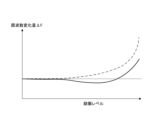
- FIG. 4 is a schematic diagram for explaining the frequency change amount characteristic (DLD characteristic) according to the excitation level.
- ⁇ F which is the amount of change in frequency
- ⁇ F simply increases monotonically as the excitation level increases, as indicated by the dashed line. That is, the accuracy of the resonance frequency F simply decreases as the excitation level increases.
- ⁇ F is a cubic function or higher with respect to the excitation level, and has a maximum and a minimum, as indicated by the solid line
- ⁇ F is A range can be maintained that does not monotonically increase (decrease) and does not significantly degrade accuracy (as long as it does not deviate significantly from this range).
- ⁇ F is 1.0 ppm or less, which is within a much smaller range than usual (A). That is, even if the excitation level is increased, the resonance frequency F does not change significantly, and practical problems are unlikely to occur.
- the thickness T2 of the excitation electrode 122 As the thickness T2 of the excitation electrode 122 further increases, the mass M of the excitation electrode 122 increases and the effect as a weight becomes excessive, which hinders the vibration of the crystal blank 121 . As a result, the increase in CI becomes more noticeable than that in ⁇ F.
- the thickness T2 is 256.3 nm or less (Example 4)
- a CI of less than 30 ⁇ is obtained (B).
- the thickness T2 is further increased (Comparative Example 3)
- CI becomes 30 ⁇ or more, which is inappropriate for transmitting/receiving the resonance frequency signal (C).
- the gold excitation electrode 122 acts as a softening spring, and the DLD characteristics related to the vibration of the crystal blank 121 offset).
- the DLD characteristics of the crystal piece 121 can be improved by adjusting the thickness T2 of the excitation electrode 122 to a large value.
- the product of the thickness T2 and the resonance frequency F is variable other than the parameters related to the physical properties of the gold excitation electrode 122 and the crystal blank 121 . Therefore, by keeping this value within an appropriate value range, it is possible to improve the DLD characteristics of the crystal resonator element 12 and suppress the increase in CI and the like as described above.
- the thickness T2 is less than 200 nm, i.e., the product value is less than 0.01536, and the thickness T2 is greater than 300 nm, i.e., the product value is 0.02304.
- the practically acceptable range of the thickness T2 is 224.9 nm or more and 256.3 nm or less
- the range of the product of these is 0.017272 or more and 0.019684 or less (mm ⁇ MHz). More preferably, since the thickness T2 is 233.5 nm or more and 239.1 nm or less, the product range is 0.017933 or more and 0.018363 or less (mm ⁇ MHz).
- FIG. 5A shows the results when the thickness T2 is 102.0 nm (Comparative Example 1, open circles and solid line), 220.6 nm (Comparative Example 2, open squares and broken line), and 233.5 nm (Example 2, black circles and broken line).
- 4 is a graph showing measurement results of ⁇ F (Y axis: normal scale) versus excitation level (X axis: logarithmic scale).
- FIG. 5B is an enlarged view of the portion surrounded by the dashed line in FIG. 5A.
- the crystal resonator element 12 (crystal element) of the present embodiment includes the crystal piece 121 and both surfaces of the crystal piece 121 at the same positions in a plan view.
- an excitation electrode 122 located on the stratum (that is, sandwiching the underlying layer with the crystal piece 121) and having a conductive layer containing gold at a mass ratio of 90% or more.
- the value of the product of the thickness (mm) of the excitation electrode 122 and the resonance frequency (MHz) of the crystal vibrating element 12 is 0.017272 or more and 0.019684 or less.
- the value of the product is 0.017933 or more and 0.018363 or less.
- the DLD characteristics are sufficiently improved as compared with the prior art, the CI can be kept at a small value, and the crystal resonator element 12 can be vibrated efficiently in comparison with the electric power.
- the resonance frequency F may be 76.8 MHz. At this frequency, the CI can be matched to the optimum range along with the DLD characteristics.
- the crystal device 1 of this embodiment includes the above-described crystal oscillator 12 . According to this crystal device 1, a stable resonance frequency F can be obtained over a wide range even when the excitation level is changed, so that it can be stably used in electronic equipment with various excitation levels.
- the crystal vibrating element 12 of the present embodiment includes a crystal piece 121 and a pair of electrodes 122a and 122b having conductive layers located on both sides of the crystal piece 121 and having a gold content of 90% or more in mass ratio. and prepare.
- the DLD characteristic of the crystal element 12 has both forward (+) and reverse (-) portions. Therefore, the crystal resonator element 12 has improved DLD characteristics, and easily resonates in the vicinity of an appropriate frequency even when the excitation level is changed. As a result, the frequency of the crystal oscillator 12 is stabilized at startup.
- the crystal vibrating element 12 has an underlying layer between the conductive layer and the crystal piece 121 .
- the electrodes 122 a and 122 b and the crystal blank 121 can be reliably bonded in the crystal vibrating element 12 .
- the resonance frequency of the crystal vibrating element 12 is 40 MHz or more and 400 MHz or less.
- the DLD characteristics can be stabilized by setting the thickness T2 of the electrodes 122a and 122b to an appropriate range thicker than the conventional one as described above. can be improved.
- the thickness of the conductive layer of the crystal oscillator 12 is 50 nm or more and 600 nm or less.
- the DLD characteristics include the "+" portion and the "-" portion, and ⁇ F can be suppressed. Therefore, the crystal oscillator 12 has improved DLD characteristics.
- the crystal impedance of the crystal vibrating element 12 is less than 30 ⁇ . By suppressing the CI to a small value, the crystal resonator element 12 can be vibrated efficiently with low loss.
- the above-described embodiment is an example, and various modifications are possible.
- the crystal oscillator 12 which is a part of the crystal device 1, has been described, but the present invention is not limited to this.
- the crystal vibrating element 12 may be manufactured, sold, or otherwise distributed as a single unit.
- the appropriate range of the thickness T2 is considered in consideration of only the DLD characteristics and CI, but the present invention is not limited to this. Other parameters may also be considered.
- the specific configurations, materials, structures, etc. shown in the above embodiments can be changed as appropriate without departing from the scope of the present invention.
- the scope of the present invention includes the scope of the invention described in the claims and the scope of equivalents thereof.
- the present disclosure can be used for crystal elements and crystal devices.
Landscapes
- Physics & Mathematics (AREA)
- Acoustics & Sound (AREA)
- Piezo-Electric Or Mechanical Vibrators, Or Delay Or Filter Circuits (AREA)
- Electrodes Of Semiconductors (AREA)
Abstract
Description
[A1]水晶片と、
当該水晶片の両面に位置してなる金の含有量が質量比で90%以上である導電層とを有する一対の電極と、
を備える水晶素子であって、
当該水晶素子のDLD特性が正方向(+)の部分と逆方向(-)の部分とが混在する、水晶素子。
[A2]前記導電層と前記水晶片との間に下地層を有するA1記載の水晶素子。
[A3]前記水晶素子の共振周波数が40MHz以上400MHz以下である[A1]又は[A2]記載の水晶素子。
[A4]前記水晶素子の導電層の厚さが50nm以上600nm以下である[A1]~[A3]のいずれか一項に記載の水晶素子。
[A5]前記水晶素子のクリスタルインピーダンスが30Ω未満である[A1]~[A4]のいずれか一項に記載の水晶素子。
[A6]前記導電層の厚さ(mm)と前記水晶素子の共振周波数(MHz)との積の値は、0.017272以上0.019684以下である[A1]~[A5]のいずれか一項に記載の水晶素子。
[A7]前記一対の電極が平面視同一位置にある[A1]~[A6]のいずれか一項に記載の水晶素子。
[A8][A1]~[A7]のいずれか一項に記載の水晶素子を備える水晶デバイス。
本開示の別の態様は、以下の通りである。
[B1]水晶片と、
当該水晶片の両面のそれぞれ平面視同一位置にあり、前記両面上にそれぞれ位置する下地層と、当該下地層上に位置し、金の含有量が質量比で90%以上である導電層とを有する電極と、
を備える水晶素子であって、
前記導電層の厚さ(mm)と当該水晶素子の共振周波数(MHz)との積の値は、0.017272以上0.019684以下である水晶素子。
[B2]前記積の値は、0.017933以上0.018363以下である[B1]記載の水晶素子。
[B3]前記共振周波数は、76.8MHzである[B1]又は[B2]記載の水晶素子。
[B4][B1]~[B3]のいずれか一項に記載の水晶素子を備える水晶デバイス。
図1は、本実施形態の水晶デバイス1のある断面における形状を示す図である。
水晶デバイス1は、基体11と、水晶振動素子12(水晶素子)と、導電性接着剤13と、蓋体14と、部品15などを備える。
水晶片121の形状は、特に限定するものではないが、長方形が好ましい。長方形の水晶片121の長辺は、通常300μm以上1500μm以下、好ましくは500μm以上1200μm以下、特に好ましくは700μm以上1000μm以下である。また、長方形の水晶片121の短辺は、水晶片121の長辺よりも短ければ特段の制限はないが、通常100μm以上1100μm以下、好ましくは250μm以上900μm以下、特に好ましくは400μm以上700μm以下である。水晶片121の長辺に対する短辺の比は、通常0.07以上1未満、好ましくは0.25以上0.9以下、特に好ましくは0.5以上0.8以下である。
図2A~図2Cは、水晶振動素子12の振動について説明する図である。
水晶振動素子12の水晶片121は、上側電極122b及び下側電極122aの間に印加される電圧に応じた分極により、当該分極方向に垂直な面内、すなわち、水晶片121の延在方向に沿って厚み滑り振動を生じる。このとき、図2Aに示すように、近似的には励振電極122は剛体であり、単に水晶片121の上面及び下面にそれぞれ位置する錘である。
kt=k1・k2/(k1+k2) … (数式1)
u2=T2・a1/V2 … (数式2)
V2は、上記剛性率と質量に依存した、すなわち、励振電極122の材質に基づく定数であり、当該材質における厚み滑りの音速である。よって、振幅u2は、励振レベル及び共振周波数Fに依存する。
F=(kt/M)1/2/(2πT1) … (数式3)
上記のように水晶片121の厚さT1は共振周波数に応じた規定値であり、励振電極122の質量Mは当該励振電極122の厚さT2に依存する。合成された非線形のばね定数ktは、上記のように水晶片121の振幅u1に依存する成分と、励振電極122の振幅u2に依存する成分とを有する。上記から、振幅u1は、励振レベルに依存し、振幅u2は、励振レベル及び厚さT2、励振レベル及び共振周波数Fに依存する。
励振電極122は、例えば、平面視で円形、楕円形若しくは多角形又はこれらの一部ずつの組み合わせであってもよい。また、励振電極122は、上記多角形の角が丸められていてもよい。励振電極122が平面視で多角形である(角が丸められているものを含む)場合には、当該多角形は長方形が好ましい。この場合、励振電極122の長辺は、水晶片121の長辺よりも短ければ特段の制限はないが、通常100μm以上1100μm以下、好ましくは250μm以上900μm以下、特に好ましくは400μm以上700μm以下である。水晶片121の長辺に対する励振電極122の長辺の比は、通常0.07以上1未満、好ましくは0.25以上0.9以下、特に好ましくは0.5以上0.8以下である。平面視長方形の励振電極122の長辺に対する短辺の比は、通常0.05以上1未満、好ましくは0.2以上0.75以下、特に好ましくは0.3以上0.5以下である。
励振電極122の構成要素である上側電極122b及び下側電極122aの形状及び大きさは、同一であってもよいし、互いに異なっていてもよい。励振電極122は、水晶片121の両面のそれぞれ平面視同一位置にあることが好ましい。ここで、平面視同一位置とは、励振電極122が多角形である場合に、上側電極122bの各辺と、当該各辺にそれぞれ対応する下側電極122aの辺とが、平面視で互いに±5μm以内の範囲に位置していることをいう。
この図表は、設定された共振周波数Fが76.8MHzであり、それぞれ略矩形状の水晶片121(ATカット、厚み:21.5μm)を長辺が805μm、短辺が537μmとし、当該水晶片121の両面に配置される励振電極122(金の含有量:99%以上)を長辺が559μm、短辺が233μmとし、水晶片と励振電極の間の下地層を材料がクロム(Cr)、厚みが4nmとした場合に、各励振電極122の厚さT2の試作品において励振レベルを変化させたときの計測結果を含んでいる。ここで、励振電極122の寸法の公差、及び水晶片121の寸法の公差は、それぞれ±10μm程度である。
ΔFは、励振レベルの変化に応じた周波数の変化幅を示している。具体的には、ΔFは、励振レベルに応じた周波数と励振レベル0.00μW時の周波数との差分を示す。従来の製品との比較上、励振レベル(励振電力)を250μWとした際にΔFが0ppm以上であればスプリアス発振が発生しにくいため好ましく、6ppm以下であれば、誤動作を避けて実用に耐えるレベルと判断している。
DLD特性は、ΔFが励振レベルに対して3次以上の関数に従って変化して、少なくとも極小値をとることが好ましい。より好ましくは、DLD特性において、ΔFが0から極小値まで単調減少する。更に好ましくは、「-」の部分において、当該グラフにおける0.01μWにおけるΔFの測定値と極小値とを結ぶ直線の傾き(Hz/μW)が-20.0以上である。より好ましくは、この傾きが-10.0以上であり、特に好ましくは、傾きが-7.5以上である。一方、「+」の部分において、当該グラフにおける極小値と250μWでのΔFの測定値とを結ぶ直線の傾き(Hz/μW)は、1.0×10-1以下であることが好ましい。より好ましくはこの傾きが5.0×10-2以下であり、更に好ましくは傾きが1.0×10-2以下であり、特に好ましくは傾きが5.0×10-3以下である。
本開示に係るCIは、具体的には、ネットワークアナライザを用いて測定される。
水晶振動素子12において、共振周波数に対する励振電極122の厚さT2をこのように定めることによって、DLD特性を改善し、励振レベルを上昇させても適正な共振周波数Fを保つことができる。
したがって、水晶振動素子12は、DLD特性が改善し、励振レベルを変化させても適正な周波数の近傍で共振させやすい。これにより、水晶振動素子12は、起動時の周波数が安定する。
例えば、上記実施の形態では、水晶デバイス1の一部である水晶振動素子12について説明したが、これに限られない。水晶振動素子12が単体で製造販売など頒布されてもよい。
その他、上記実施の形態で示した具体的な構成、材質、構造などは、本発明の趣旨を逸脱しない範囲において適宜変更可能である。本発明の範囲は、特許請求の範囲に記載した発明の範囲とその均等の範囲を含む。
Claims (12)
- 水晶片と、
当該水晶片の両面に位置し、金の含有量が質量比で90%以上である導電層を有する一対の電極と、
を備える水晶素子であって、
当該水晶素子のDLD特性が正方向(+)の部分と逆方向(-)の部分とが混在する、水晶素子。 - 前記導電層と前記水晶片との間に下地層を有する、請求項1に記載の水晶素子。
- 前記水晶素子の共振周波数が40MHz以上400MHz以下である、請求項1又は2に記載の水晶素子。
- 前記水晶素子の導電層の厚さが50nm以上600nm以下である、請求項1~3のいずれか一項に記載の水晶素子。
- 前記水晶素子のクリスタルインピーダンスが30Ω未満である、請求項1~4のいずれか一項に記載の水晶素子。
- 前記導電層の厚さ(mm)と前記水晶素子の共振周波数(MHz)との積の値は、0.017272以上0.019684以下である、請求項1~5のいずれか一項に記載の水晶素子。
- 前記一対の電極が平面視同一位置にある、請求項1~6のいずれか一項に記載の水晶素子。
- 請求項1~7のいずれか一項に記載の水晶素子を備える水晶デバイス。
- 水晶片と、
当該水晶片の両面のそれぞれ平面視同一位置にあり、前記両面上にそれぞれ位置する下地層と、当該下地層上に位置し、金の含有量が質量比で90%以上である導電層とを有する電極と、
を備える水晶素子であって、
前記導電層の厚さ(mm)と当該水晶素子の共振周波数(MHz)との積の値は、0.017272以上0.019684以下である
水晶素子。 - 前記積の値は、0.017933以上0.018363以下である請求項9に記載の水晶素子。
- 前記共振周波数は、76.8MHzである請求項9又は10に記載の水晶素子。
- 請求項9~11のいずれか一項に記載の水晶素子を備える水晶デバイス。
Priority Applications (3)
| Application Number | Priority Date | Filing Date | Title |
|---|---|---|---|
| US18/710,008 US20250015778A1 (en) | 2021-11-15 | 2022-11-10 | Crystal element and crystal device |
| CN202280074093.5A CN118202572A (zh) | 2021-11-15 | 2022-11-10 | 水晶元件以及水晶设备 |
| JP2023559885A JP7630010B2 (ja) | 2021-11-15 | 2022-11-10 | 水晶素子及び水晶デバイス |
Applications Claiming Priority (2)
| Application Number | Priority Date | Filing Date | Title |
|---|---|---|---|
| JP2021-185693 | 2021-11-15 | ||
| JP2021185693 | 2021-11-15 |
Publications (1)
| Publication Number | Publication Date |
|---|---|
| WO2023085348A1 true WO2023085348A1 (ja) | 2023-05-19 |
Family
ID=86335822
Family Applications (1)
| Application Number | Title | Priority Date | Filing Date |
|---|---|---|---|
| PCT/JP2022/041864 Ceased WO2023085348A1 (ja) | 2021-11-15 | 2022-11-10 | 水晶素子及び水晶デバイス |
Country Status (5)
| Country | Link |
|---|---|
| US (1) | US20250015778A1 (ja) |
| JP (1) | JP7630010B2 (ja) |
| CN (1) | CN118202572A (ja) |
| TW (1) | TWI841052B (ja) |
| WO (1) | WO2023085348A1 (ja) |
Citations (6)
| Publication number | Priority date | Publication date | Assignee | Title |
|---|---|---|---|---|
| JP2001251160A (ja) * | 2000-03-07 | 2001-09-14 | Seiko Epson Corp | 圧電振動片及びその製造方法 |
| JP2007096945A (ja) * | 2005-09-29 | 2007-04-12 | Daishinku Corp | 水晶振動デバイスおよび水晶振動デバイスの製造方法 |
| JP2013255052A (ja) * | 2012-06-06 | 2013-12-19 | Seiko Epson Corp | 振動素子、振動子、電子デバイス、電子機器、移動体および振動素子の製造方法 |
| JP2014158149A (ja) * | 2013-02-15 | 2014-08-28 | Seiko Epson Corp | 振動素子、振動子、電子デバイス、電子機器、及び移動体 |
| JP2015109633A (ja) * | 2013-10-22 | 2015-06-11 | 株式会社大真空 | 圧電振動素子と当該圧電振動素子を用いた圧電デバイスおよび、前記圧電振動素子の製造方法と当該圧電振動素子を用いた圧電デバイスの製造方法 |
| JP2020136999A (ja) * | 2019-02-22 | 2020-08-31 | 京セラ株式会社 | 水晶素子、水晶デバイス及び電子機器 |
-
2022
- 2022-11-10 JP JP2023559885A patent/JP7630010B2/ja active Active
- 2022-11-10 CN CN202280074093.5A patent/CN118202572A/zh active Pending
- 2022-11-10 WO PCT/JP2022/041864 patent/WO2023085348A1/ja not_active Ceased
- 2022-11-10 US US18/710,008 patent/US20250015778A1/en active Pending
- 2022-11-14 TW TW111143368A patent/TWI841052B/zh active
Patent Citations (6)
| Publication number | Priority date | Publication date | Assignee | Title |
|---|---|---|---|---|
| JP2001251160A (ja) * | 2000-03-07 | 2001-09-14 | Seiko Epson Corp | 圧電振動片及びその製造方法 |
| JP2007096945A (ja) * | 2005-09-29 | 2007-04-12 | Daishinku Corp | 水晶振動デバイスおよび水晶振動デバイスの製造方法 |
| JP2013255052A (ja) * | 2012-06-06 | 2013-12-19 | Seiko Epson Corp | 振動素子、振動子、電子デバイス、電子機器、移動体および振動素子の製造方法 |
| JP2014158149A (ja) * | 2013-02-15 | 2014-08-28 | Seiko Epson Corp | 振動素子、振動子、電子デバイス、電子機器、及び移動体 |
| JP2015109633A (ja) * | 2013-10-22 | 2015-06-11 | 株式会社大真空 | 圧電振動素子と当該圧電振動素子を用いた圧電デバイスおよび、前記圧電振動素子の製造方法と当該圧電振動素子を用いた圧電デバイスの製造方法 |
| JP2020136999A (ja) * | 2019-02-22 | 2020-08-31 | 京セラ株式会社 | 水晶素子、水晶デバイス及び電子機器 |
Also Published As
| Publication number | Publication date |
|---|---|
| CN118202572A (zh) | 2024-06-14 |
| JP7630010B2 (ja) | 2025-02-14 |
| TW202327107A (zh) | 2023-07-01 |
| US20250015778A1 (en) | 2025-01-09 |
| TWI841052B (zh) | 2024-05-01 |
| JPWO2023085348A1 (ja) | 2023-05-19 |
Similar Documents
| Publication | Publication Date | Title |
|---|---|---|
| JP4281348B2 (ja) | 圧電振動片と圧電振動片を利用した圧電デバイス、ならびに圧電デバイスを利用した携帯電話装置および圧電デバイスを利用した電子機器 | |
| CN102035499B (zh) | 振动片、振子、振荡器以及电子设备 | |
| US8736152B2 (en) | Piezoelectric vibrating pieces and associated devices exhibiting enhanced electrical field | |
| CN102064793B (zh) | 振动器件及电子设备 | |
| US20130193807A1 (en) | Quartz crystal vibrating piece and quartz crystal device | |
| US8665032B2 (en) | Flexural mode resonator element, resonating device, and electronic apparatus | |
| JP5652122B2 (ja) | 振動片、振動デバイス及び電子機器 | |
| JP5040654B2 (ja) | 水晶振動子 | |
| JP5668392B2 (ja) | 圧電振動素子、圧電振動子及び圧電発振器 | |
| JP4756426B2 (ja) | 水晶振動子と水晶ユニットと水晶発振器の各製造方法 | |
| US9871469B2 (en) | Piezoelectric vibrator element, and piezoelectric vibrator | |
| JP7630010B2 (ja) | 水晶素子及び水晶デバイス | |
| JP2009290778A (ja) | 音叉型圧電振動素子 | |
| JP2004328701A (ja) | 水晶発振器の製造方法 | |
| JP5732903B2 (ja) | 振動素子、振動子、発振器、ジャイロセンサー及び電子機器 | |
| JP2012186586A (ja) | 圧電振動素子、圧電振動子、圧電発振器、振動ジャイロ素子、振動ジャイロセンサー及び電子機器 | |
| JP6845046B2 (ja) | 水晶素子および水晶デバイス | |
| JP2004236008A (ja) | 圧電振動片と圧電振動片を利用した圧電デバイス、ならびに圧電デバイスを利用した携帯電話装置および圧電デバイスを利用した電子機器 | |
| JP2007088691A (ja) | 圧電振動片および圧電デバイスとこれらの製造方法 | |
| JP2002368573A (ja) | 超薄板圧電振動子及びその製造方法 | |
| JP7723916B2 (ja) | 圧電振動素子 | |
| JP6841892B2 (ja) | 水晶素子および水晶デバイス | |
| JP7542253B2 (ja) | 水晶発振装置 | |
| WO2025182135A1 (ja) | 圧電振動子 | |
| JP6687471B2 (ja) | 水晶素子および水晶デバイス |
Legal Events
| Date | Code | Title | Description |
|---|---|---|---|
| 121 | Ep: the epo has been informed by wipo that ep was designated in this application |
Ref document number: 22892846 Country of ref document: EP Kind code of ref document: A1 |
|
| WWE | Wipo information: entry into national phase |
Ref document number: 202280074093.5 Country of ref document: CN |
|
| ENP | Entry into the national phase |
Ref document number: 2023559885 Country of ref document: JP Kind code of ref document: A |
|
| WWE | Wipo information: entry into national phase |
Ref document number: 18710008 Country of ref document: US |
|
| 122 | Ep: pct application non-entry in european phase |
Ref document number: 22892846 Country of ref document: EP Kind code of ref document: A1 |