WO2023085285A1 - 検出装置 - Google Patents
検出装置 Download PDFInfo
- Publication number
- WO2023085285A1 WO2023085285A1 PCT/JP2022/041609 JP2022041609W WO2023085285A1 WO 2023085285 A1 WO2023085285 A1 WO 2023085285A1 JP 2022041609 W JP2022041609 W JP 2022041609W WO 2023085285 A1 WO2023085285 A1 WO 2023085285A1
- Authority
- WO
- WIPO (PCT)
- Prior art keywords
- light
- light guide
- layer
- guide plate
- detection
- Prior art date
- Legal status (The legal status is an assumption and is not a legal conclusion. Google has not performed a legal analysis and makes no representation as to the accuracy of the status listed.)
- Ceased
Links
Images








Classifications
-
- G—PHYSICS
- G01—MEASURING; TESTING
- G01J—MEASUREMENT OF INTENSITY, VELOCITY, SPECTRAL CONTENT, POLARISATION, PHASE OR PULSE CHARACTERISTICS OF INFRARED, VISIBLE OR ULTRAVIOLET LIGHT; COLORIMETRY; RADIATION PYROMETRY
- G01J1/00—Photometry, e.g. photographic exposure meter
- G01J1/42—Photometry, e.g. photographic exposure meter using electric radiation detectors
-
- G—PHYSICS
- G01—MEASURING; TESTING
- G01J—MEASUREMENT OF INTENSITY, VELOCITY, SPECTRAL CONTENT, POLARISATION, PHASE OR PULSE CHARACTERISTICS OF INFRARED, VISIBLE OR ULTRAVIOLET LIGHT; COLORIMETRY; RADIATION PYROMETRY
- G01J1/00—Photometry, e.g. photographic exposure meter
- G01J1/02—Details
- G01J1/04—Optical or mechanical part supplementary adjustable parts
- G01J1/0407—Optical elements not provided otherwise, e.g. manifolds, windows, holograms, gratings
-
- G—PHYSICS
- G06—COMPUTING OR CALCULATING; COUNTING
- G06V—IMAGE OR VIDEO RECOGNITION OR UNDERSTANDING
- G06V40/00—Recognition of biometric, human-related or animal-related patterns in image or video data
- G06V40/10—Human or animal bodies, e.g. vehicle occupants or pedestrians; Body parts, e.g. hands
-
- H—ELECTRICITY
- H10—SEMICONDUCTOR DEVICES; ELECTRIC SOLID-STATE DEVICES NOT OTHERWISE PROVIDED FOR
- H10F—INORGANIC SEMICONDUCTOR DEVICES SENSITIVE TO INFRARED RADIATION, LIGHT, ELECTROMAGNETIC RADIATION OF SHORTER WAVELENGTH OR CORPUSCULAR RADIATION
- H10F30/00—Individual radiation-sensitive semiconductor devices in which radiation controls the flow of current through the devices, e.g. photodetectors
- H10F30/20—Individual radiation-sensitive semiconductor devices in which radiation controls the flow of current through the devices, e.g. photodetectors the devices having potential barriers, e.g. phototransistors
-
- H—ELECTRICITY
- H10—SEMICONDUCTOR DEVICES; ELECTRIC SOLID-STATE DEVICES NOT OTHERWISE PROVIDED FOR
- H10F—INORGANIC SEMICONDUCTOR DEVICES SENSITIVE TO INFRARED RADIATION, LIGHT, ELECTROMAGNETIC RADIATION OF SHORTER WAVELENGTH OR CORPUSCULAR RADIATION
- H10F39/00—Integrated devices, or assemblies of multiple devices, comprising at least one element covered by group H10F30/00, e.g. radiation detectors comprising photodiode arrays
- H10F39/10—Integrated devices
- H10F39/12—Image sensors
-
- H—ELECTRICITY
- H10—SEMICONDUCTOR DEVICES; ELECTRIC SOLID-STATE DEVICES NOT OTHERWISE PROVIDED FOR
- H10F—INORGANIC SEMICONDUCTOR DEVICES SENSITIVE TO INFRARED RADIATION, LIGHT, ELECTROMAGNETIC RADIATION OF SHORTER WAVELENGTH OR CORPUSCULAR RADIATION
- H10F55/00—Radiation-sensitive semiconductor devices covered by groups H10F10/00, H10F19/00 or H10F30/00 being structurally associated with electric light sources and electrically or optically coupled thereto
Definitions
- the present invention relates to a detection device.
- Optical sensors capable of detecting fingerprint patterns and vein patterns are known (for example, Patent Documents 1 and 2).
- the optical sensors described in Patent Literatures 1 and 2 are provided with a front light on the front side of a plurality of photodiodes.
- a collimator having a plurality of light guide paths and a light blocking portion is provided between the plurality of photodiodes and the front light.
- JP 2019-045503 A JP-A-11-120324
- an optical sensor in which a front light is provided between an object to be detected such as a finger and a plurality of photodiodes, it is necessary to guide light from the object to be detected such as a finger to the plurality of photodiodes.
- the light that is directly incident on the plurality of photodiodes on the side opposite to the detection object such as the finger may reduce the detection contrast.
- part of the light emitted from the front light may be absorbed by the light shielding portion of the collimator, which may reduce the light utilization efficiency.
- An object of the present invention is to provide a detection device that has a front light and is capable of obtaining good detection accuracy.
- a detection device includes a plurality of photodiodes arranged on a substrate, a light guide plate arranged so as to overlap the plurality of photodiodes, and a light source that irradiates a side surface of the light guide plate with light. and an optical filter layer provided between the plurality of photodiodes and the light guide plate of the frontlight, wherein the optical filter layer at least partially overlaps the photodiodes.
- the optical filter layer including a plurality of light guide paths and a light shielding section having a higher absorption rate of the light than the light guide paths, and between the light guide plate and the light filter layer and with the light shielding section of the light filter layer It has a reflective layer provided in the overlapping region.
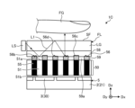
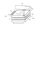
- FIG. 1 is a perspective view schematically showing the detection device according to the first embodiment.
- FIG. 2 is a cross-sectional view showing a schematic cross-sectional configuration of the detection device according to the first embodiment.
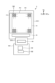
- FIG. 3 is a plan view showing the detection device according to the first embodiment.
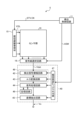
- FIG. 4 is a block diagram showing a configuration example of the detection device according to the first embodiment.
- FIG. 5 is a circuit diagram showing a sensing element.
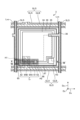
- FIG. 6 is a plan view schematically showing the detection element according to the first embodiment.
- FIG. 7 is a cross-sectional view taken along line VII-VII' of FIG.
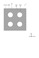
- FIG. 8 is a plan view for explaining the positional relationship among photodiodes, optical filter layers, and reflective layers.
- FIG. 1 is a perspective view schematically showing the detection device according to the first embodiment.
- FIG. 2 is a cross-sectional view showing a schematic cross-sectional configuration of the detection device according to the first embodiment.
- FIG. 3 is a plan
- FIG. 9 is a cross-sectional view schematically showing a cross section of a detection device according to a comparative example.
- FIG. 10 is a cross-sectional view showing a schematic cross-sectional configuration of a detection device according to the second embodiment.
- FIG. 11 is a cross-sectional view showing the scattering section of the detection device according to the second embodiment.
- FIG. 12 is a cross-sectional view showing a schematic cross-sectional configuration of the detection device according to the third embodiment.
- FIG. 13 is a cross-sectional view showing a schematic cross-sectional configuration of the detection device according to the fourth embodiment.
- FIG. 14 is a cross-sectional view showing an inclined portion of a reflective layer of a detection device according to a fourth embodiment.
- FIG. 15 is a perspective view schematically showing the detection device according to the fifth embodiment.
- FIG. 16 is a cross-sectional view showing a schematic cross-sectional configuration of the detection device according to the fifth embodiment.
- FIG. 1 is a perspective view schematically showing the detection device according to the first embodiment.
- FIG. 2 is a cross-sectional view showing a schematic cross-sectional configuration of the detection device according to the first embodiment.
- the detection device 1 includes an optical sensor 5, a light filter layer 50 and a front light FL.
- An optical filter layer 50 and a front light FL are laminated in this order on the optical sensor 5 .
- the optical sensor 5 has an array substrate 2 and a plurality of detection elements 3 (photodiodes 30) formed on the array substrate 2.
- the array substrate 2 is formed using the substrate 21 as a base. Further, each of the plurality of detection elements 3 includes a photodiode 30, a plurality of transistors, and various wirings.
- the array substrate 2 on which the photodiodes 30 are formed is a driving circuit substrate that drives sensors for each predetermined detection area, and is also called a backplane or an active matrix substrate.
- the optical filter layer 50 is arranged to face the plurality of photodiodes 30, and is arranged between the plurality of photodiodes 30, the light guide plate LG of the front light FL, and the detection object FG such as a finger.
- the optical filter layer 50 has a plurality of light guide paths 51 and a light blocking portion 55 provided around the plurality of light guide paths 51 . At least part of the light guide path 51 overlaps the photodiode 30 . Also, the light shielding portion 55 has a higher light absorption rate than the light guide path 51 .
- the optical filter layer 50 is an optical element that transmits, toward the photodiode 30, a component traveling in the third direction Dz among the light reflected by the detection object FG such as a finger.
- the optical filter layer 50 is also called a collimating aperture or a collimator.
- the first direction Dx is one direction within a plane parallel to the substrate 21 .
- the second direction Dy is one direction in a plane parallel to the substrate 21 and perpendicular to the first direction Dx. Note that the second direction Dy may cross the first direction Dx instead of being perpendicular to it.
- a third direction Dz is a direction orthogonal to the first direction Dx and the second direction Dy, and is a normal direction of the main surface of the substrate 21 .
- “planar view” refers to the positional relationship when viewed from a direction perpendicular to the substrate 21 .
- the front light FL is arranged above the optical filter layer 50 , that is, on the front side of the optical sensor 5 and the optical filter layer 50 .
- the front light FL has a translucent light guide plate LG, a light source LS facing the side surface of the light guide plate LG, and a plurality of scattering portions SC11. Although illustration is omitted, the optical filter layer 50 and the front light FL are joined with an optical resin.
- a space air layer may be provided between the light filter layer 50 and the front light FL.
- the light source LS is, for example, a light emitting diode (LED) that emits red light or infrared light.
- the light source LS is not limited to this, and can be appropriately changed depending on the measurement item such as green.
- a plurality of LEDs of the light source LS are arranged along the side surface of the light guide plate LG.
- the light guide plate LG is arranged so as to overlap the plurality of photodiodes 30 . Further, the detection target FG is arranged to face the detection surface SF of the light guide plate LG.
- the plurality of scattering portions SC11 are provided on the surface of the light guide plate LG opposite to the detection surface SF, that is, the surface of the light guide plate LG facing the optical filter layer 50 . Moreover, the plurality of scattering portions SC11 are provided in regions overlapping the light shielding portions 55 of the optical filter layer 50 .
- the scattering portion SC11 is a prism-shaped (triangular) concave portion or convex portion. However, the scattering portions SC11 may be dot-shaped concave portions or convex portions.
- the detection device 1 has a reflective layer 56 provided between the light guide plate LG and the optical filter layer 50 .
- the reflective layer 56 is provided in a region overlapping the light shielding portion 55 of the optical filter layer 50 . Moreover, the reflective layer 56 is not provided in the region of the optical filter layer 50 overlapping the light guide path 51 .
- the reflective layer 56 is a plate-shaped member made of a metal material, and is provided parallel to the surface of the light guide plate LG facing the optical filter layer 50 .
- the reflective layer 56 is provided on and in direct contact with the light shielding portion 55 . However, it is not limited to this, and may be provided on the light shielding portion 55 via a resin layer or the like.
- the light emitted from the light source LS propagates through the light guide plate LG while repeating total reflection on the detection surface SF and the back surface.
- Part of the light propagating through the light guide plate LG is scattered by the scattering portion SC11.
- a part of the light scattered by the scattering part SC11 is emitted from the detection surface SF of the light guide plate LG to the detection object FG.
- Part of the light reflected by the object to be detected FG passes through the light guide plate LG and the light guide path 51 of the light filter layer 50 and is irradiated onto the plurality of photodiodes 30 .
- the plurality of photodiodes 30 of the optical sensor 5 can detect information about the detection object FG using the light emitted from the light source LS.
- the light scattered by the scattering part SC11 includes a component emitted to the light filter layer 50 facing the light guide plate LG, in addition to the component emitted to the detection object FG side. Since the scattering portion SC11 is provided in a region overlapping the light blocking portion 55 and the reflecting layer 56 of the optical filter layer 50, the light scattered toward the optical filter layer 50 by the scattering portion SC11 does not enter the light guide path 51 and is reflected. It is reflected by the layer 56 and returns to the light guide plate LG.
- the photodiode 30 of the optical sensor 5 is mainly irradiated with the light reflected by the object to be detected FG.
- the detection device 1 having the front light FL can improve detection accuracy.
- the light scattered toward the optical filter layer 50 by the scattering portion SC11 is not absorbed by the light shielding portion 55 of the optical filter layer 50, but is reflected by the reflective layer 56 and reused. Accordingly, since the detection device 1 is provided with the reflective layer 56, it is possible to improve the light utilization efficiency.
- the detectable object FG is, for example, a finger, palm, wrist, or the like.
- the optical sensor 5 can detect information such as the fingerprint of the detection object FG based on light.
- the optical sensor 5 may detect various information (biological information) such as the shape of a blood vessel, pulse, and pulse wave. That is, the detection device 1 may be configured as a fingerprint detection device that detects fingerprints or a vein detection device that detects blood vessel patterns such as veins.
- the light source LS that the front light FL has is not limited to one type, and a plurality of types having different wavelengths may be provided.
- FIG. 3 is a plan view showing the detection device according to the first embodiment.
- the optical sensor 5 included in the detection device 1 includes a substrate 21 (array substrate 2), a sensor section 10, a scanning line driving circuit 15, a signal line selection circuit 16, a detection circuit 48, It has a control circuit 102 and a power supply circuit 103 .
- a control board 501 is electrically connected to the board 21 via a wiring board 510 .
- the wiring board 510 is, for example, a flexible printed board or a rigid board.
- a detection circuit 48 is provided on the wiring board 510 .
- a control circuit 102 and a power supply circuit 103 are provided on the control board 501 .
- the control circuit 102 is, for example, an FPGA (Field Programmable Gate Array).
- the control circuit 102 supplies control signals to the sensor section 10 , the scanning line driving circuit 15 and the signal line selection circuit 16 to control the detection operation of the sensor section 10 .
- the control circuit 102 also supplies a control signal to the front light FL (see FIGS. 1 and 2) to control lighting or non-lighting of the light source LS.
- the power supply circuit 103 supplies voltage signals such as the power supply potential SVS and the reference potential VR1 (see FIG. 5) to the sensor section 10, the scanning line driving circuit 15, and the signal line selecting circuit 16.
- FIG. 5 the power supply potential SVS and
- the substrate 21 has a detection area AA and a peripheral area GA.
- the detection area AA is an area in which a plurality of photodiodes 30 of the sensor section 10 are provided.
- the peripheral area GA is an area between the outer circumference of the detection area AA and the outer edge of the substrate 21, and is an area where the plurality of photodiodes 30 are not provided.
- the scanning line drive circuit 15 and the signal line selection circuit 16 are provided in the peripheral area GA. Specifically, the scanning line driving circuit 15 is provided in a region extending along the second direction Dy in the peripheral region GA.
- the signal line selection circuit 16 is provided in an area extending along the first direction Dx in the peripheral area GA, and is provided between the sensor section 10 and the detection circuit 48 .
- the plurality of detection elements 3 of the sensor section 10 are optical sensors each having a photodiode 30 as a sensor element.
- the photodiode 30 is a photoelectric conversion element, and outputs an electric signal according to the light with which it is irradiated. More specifically, the photodiode 30 is a PIN (Positive Intrinsic Negative) photodiode or an OPD (Organic Photodiode) using an organic semiconductor.
- a plurality of detection elements 3 (photodiodes 30) are arranged in a matrix in the detection area AA.
- the photodiodes 30 included in the plurality of detection elements 3 perform detection according to gate drive signals supplied from the scanning line drive circuit 15 .
- the plurality of photodiodes 30 output an electrical signal corresponding to the light irradiated to each to the signal line selection circuit 16 as the detection signal Vdet.
- the detection device 1 detects information about the detected object FG based on the detection signals Vdet from the plurality of photodiodes 30 .
- FIG. 4 is a block diagram showing a configuration example of the detection device according to the first embodiment.
- the detection device 1 further has a detection control circuit 11 and a detection section 40 .
- a part or all of the functions of the detection control circuit 11 are included in the control circuit 102 .
- a part or all of the functions of the detection unit 40 other than the detection circuit 48 are included in the control circuit 102 .
- the detection control circuit 11 is a circuit that supplies control signals to the scanning line drive circuit 15, the signal line selection circuit 16, and the detection section 40, respectively, and controls their operations.
- the detection control circuit 11 supplies the scanning line driving circuit 15 with various control signals such as a start signal STV, a clock signal CK, and a reset signal RST1.
- the detection control circuit 11 also supplies various control signals such as the selection signal ASW to the signal line selection circuit 16 .
- the scanning line drive circuit 15 is a circuit that drives a plurality of scanning lines GLS (see FIG. 5) based on various control signals.
- the scanning line driving circuit 15 sequentially or simultaneously selects a plurality of scanning lines GLS and supplies gate driving signals VGL to the selected scanning lines GLS. Thereby, the scanning line driving circuit 15 selects a plurality of photodiodes 30 connected to the scanning line GLS.
- the signal line selection circuit 16 is a switch circuit that sequentially or simultaneously selects a plurality of output signal lines SLS (see FIG. 5).
- the signal line selection circuit 16 is, for example, a multiplexer.
- the signal line selection circuit 16 connects the selected output signal line SLS and the detection circuit 48 based on the selection signal ASW supplied from the detection control circuit 11 . Thereby, the signal line selection circuit 16 outputs the detection signal Vdet of the photodiode 30 to the detection section 40 .
- the detection unit 40 includes a detection circuit 48 , a signal processing circuit 44 , a coordinate extraction circuit 45 , a storage circuit 46 and a detection timing control circuit 47 .
- the detection timing control circuit 47 controls the detection circuit 48, the signal processing circuit 44, and the coordinate extraction circuit 45 to operate synchronously based on the control signal supplied from the detection control circuit 11.
- the detection circuit 48 is, for example, an analog front end circuit (AFE, Analog Front End).
- the detection circuit 48 is a signal processing circuit having at least the functions of the detection signal amplification circuit 42 and the A/D conversion circuit 43 .
- the detection signal amplifier circuit 42 amplifies the detection signal Vdet.
- the A/D conversion circuit 43 converts the analog signal output from the detection signal amplification circuit 42 into a digital signal.
- the signal processing circuit 44 is a logic circuit that detects a predetermined physical quantity input to the sensor section 10 based on the output signal of the detection circuit 48 .
- the signal processing circuit 44 can detect the unevenness of the surface of the finger or palm based on the signal from the detection circuit 48 when the finger touches or approaches the detection surface SF (light guide plate LG). Also, the signal processing circuit 44 can detect information about the living body based on the signal from the detection circuit 48 .
- the biological information includes, for example, finger and palm blood vessel images, pulse waves, pulse, blood oxygen concentration, and the like.
- the storage circuit 46 temporarily stores the signal calculated by the signal processing circuit 44 .
- the storage circuit 46 may be, for example, a RAM (Random Access Memory), a register circuit, or the like.
- the coordinate extraction circuit 45 is a logic circuit that obtains the detected coordinates of the unevenness of the surface of the finger or the like when the signal processing circuit 44 detects contact or proximity of the finger.
- a coordinate extraction circuit 45 is a logic circuit for obtaining the detected coordinates of the blood vessels of the fingers and palms.
- the coordinate extraction circuit 45 combines the detection signals Vdet output from the photodiodes 30 of the sensor unit 10 to obtain two-dimensional information indicating the shape of the uneven surface of the finger or the like and two-dimensional information indicating the shape of the blood vessels of the finger or palm. Generate information. Note that the coordinate extraction circuit 45 may output the detection signal Vdet as the sensor output voltage Vo without calculating the detection coordinates.
- FIG. 5 is a circuit diagram showing a sensing element.
- the detection element 3 includes a photodiode 30, a capacitive element Ca, and a first transistor Tr.
- a first transistor Tr is provided corresponding to the photodiode 30 .
- the first transistor Tr is configured by a thin film transistor, and in this example, is configured by an n-channel MOS (Metal Oxide Semiconductor) type TFT (Thin Film Transistor).
- a gate of the first transistor Tr is connected to the scanning line GLS.
- the source of the first transistor Tr is connected to the output signal line SLS.
- the drain of the first transistor Tr is connected to the anode of the photodiode 30 and the capacitive element Ca.
- a power supply potential SVS is supplied from the power supply circuit 103 to the cathode of the photodiode 30 .
- a reference potential VR1 which is an initial potential of the capacitor Ca, is supplied from the power supply circuit 103 to the capacitor Ca.
- the detection device 1 When the detection element 3 is irradiated with light, a current corresponding to the amount of light flows through the photodiode 30, thereby accumulating charges in the capacitive element Ca. When the first transistor Tr is turned on, current flows through the output signal line SLS according to the charge accumulated in the capacitive element Ca. The output signal line SLS is connected to the detection circuit 48 via the signal line selection circuit 16 . Thereby, the detection device 1 can detect a signal corresponding to the light amount of the light irradiated to the photodiode 30 for each detection element 3 .
- the scanning line GLS and the output signal line SLS are connected to multiple detection elements 3 .
- the scanning line GLS extends in the first direction Dx (see FIG. 3) and is connected to the plurality of detection elements 3 arranged in the first direction Dx.
- the output signal line SLS extends in the second direction Dy and is connected to the plurality of detection elements 3 arranged in the second direction Dy.
- the first transistor Tr is not limited to an n-type TFT, and may be composed of a p-type TFT. Also, in the detection element 3 , a plurality of transistors may be provided corresponding to one photodiode 30 .
- FIG. 6 is a plan view schematically showing the detection element according to the first embodiment.
- the detection element 3 is an area surrounded by the scanning lines GLS and the output signal lines SLS.
- the scanning lines GLS include first scanning lines GLA and second scanning lines GLB.
- the first scanning line GLA is provided so as to overlap with the second scanning line GLB.
- the first scanning line GLA and the second scanning line GLB are provided in different layers with insulating layers 22c and 22d (see FIG. 7) interposed therebetween.
- the first scanning line GLA and the second scanning line GLB are electrically connected at an arbitrary point and supplied with a gate drive signal VGL having the same potential.
- At least one of the first scanning line GLA and the second scanning line GLB is connected to the scanning line driving circuit 15 .
- the first scanning line GLA and the second scanning line GLB have different widths in FIG. 6, they may have the same width.
- the photodiode 30 is provided in a region surrounded by the scanning line GLS and the output signal line SLS.
- the upper electrode 34 and the lower electrode 35 are provided corresponding to each photodiode 30 .
- Photodiode 30 is, for example, a PIN photodiode.
- the lower electrode 35 is, for example, the anode electrode of the photodiode 30 .
- the upper electrode 34 is, for example, the cathode electrode of the photodiode 30 .
- the upper electrode 34 is connected to the power signal line Lvs via the connection wiring 36 .
- the power signal line Lvs is a wiring that supplies the power potential SVS to the photodiode 30 .
- the power signal line Lvs overlaps the output signal line SLS and extends in the second direction Dy.
- a plurality of detection elements 3 arranged in the second direction Dy are connected to a common power signal line Lvs. With such a configuration, the aperture of the detection element 3 can be enlarged.
- the lower electrode 35, the photodiode 30, and the upper electrode 34 are substantially rectangular in plan view. However, it is not limited to this, and the shapes of the lower electrode 35, photodiode 30 and upper electrode 34 can be changed as appropriate.
- the first transistor Tr is provided near the intersection between the scanning line GLS and the output signal line SLS.
- the first transistor Tr includes a semiconductor layer 61, a source electrode 62, a drain electrode 63, a first gate electrode 64A and a second gate electrode 64B.
- the semiconductor layer 61 is an oxide semiconductor. More preferably, the semiconductor layer 61 is a transparent amorphous oxide semiconductor (TAOS) among oxide semiconductors. Leakage current of the first transistor Tr can be suppressed by using an oxide semiconductor for the first transistor Tr. That is, the first transistor Tr can reduce the leak current from the unselected detection element 3 . Therefore, the detection device 1 can improve the S/N ratio.
- the semiconductor layer 61 is not limited to this, and may be a microcrystalline oxide semiconductor, an amorphous oxide semiconductor, polysilicon, low temperature polysilicon (LTPS: Low Temperature Polycrystalline Silicon), or the like.
- the semiconductor layer 61 is provided along the first direction Dx and intersects the first gate electrode 64A and the second gate electrode 64B in plan view.
- the first gate electrode 64A and the second gate electrode 64B are branched from the first scanning line GLA and the second scanning line GLB, respectively.
- the portions of the first scanning line GLA and the second scanning line GLB that overlap the semiconductor layer 61 function as the first gate electrode 64A and the second gate electrode 64B.
- Aluminum (Al), copper (Cu), silver (Ag), molybdenum (Mo), or an alloy thereof is used for the first gate electrode 64A and the second gate electrode 64B.
- a channel region is formed in a portion of the semiconductor layer 61 overlapping with the first gate electrode 64A and the second gate electrode 64B.
- One end of the semiconductor layer 61 is connected to the source electrode 62 through the contact hole H1.
- the other end of the semiconductor layer 61 is connected to the drain electrode 63 through the contact hole H2.
- a portion of the output signal line SLS that overlaps with the semiconductor layer 61 is the source electrode 62 .
- a portion of the third conductive layer 67 that overlaps with the semiconductor layer 61 functions as a drain electrode 63 .
- Third conductive layer 67 is connected to lower electrode 35 through contact hole H3.
- the arrangement pitch of the detection elements 3 (photodiodes 30) in the first direction Dx is defined by the arrangement pitch of the output signal lines SLS in the first direction Dx.
- the arrangement pitch of the detection elements 3 (photodiodes 30) in the second direction Dy is defined by the arrangement pitch of the scanning lines GLS in the second direction Dy.
- FIG. 7 is a cross-sectional view taken along line VII-VII' of FIG.
- a cross section along the line VII-VII' and a first plane of the peripheral area GA are shown.
- a cross section of a portion including two transistors TrG is schematically shown connected.
- cross sections of a portion including the terminal portion 72 of the peripheral area GA are schematically connected and shown.
- the direction from the substrate 21 to the photodiode 30 in the direction (third direction Dz) perpendicular to the surface of the substrate 21 is defined as “upper” or “upper”.
- the direction from the photodiode 30 to the substrate 21 is defined as “lower side” or “lower side”.
- the substrate 21 is an insulating substrate, and for example, a glass substrate such as quartz or alkali-free glass is used.
- the first transistor Tr, various wirings (scanning line GLS and output signal line SLS), and an insulating layer are provided on one surface of the substrate 21 to form the array substrate 2 .
- the photodiodes 30 are arranged on the array substrate 2 , that is, on one side of the substrate 21 .
- the substrate 21 may be a resin substrate or a resin film made of resin such as polyimide.
- the insulating layers 22 a and 22 b are provided on the substrate 21 .
- the insulating layers 22a, 22b, 22c, 22d, 22e, 22f, and 22g are inorganic insulating films such as silicon oxide (SiO 2 ) and silicon nitride (SiN).
- each inorganic insulating layer is not limited to a single layer, and may be a laminated film.
- the first gate electrode 64A is provided on the insulating layer 22b.
- the insulating layer 22c is provided on the insulating layer 22b to cover the first gate electrode 64A.
- the semiconductor layer 61, the first conductive layer 65 and the second conductive layer 66 are provided on the insulating layer 22c.
- the first conductive layer 65 is provided to cover the end portion of the semiconductor layer 61 that is connected to the source electrode 62 .
- the second conductive layer 66 is provided to cover the end of the semiconductor layer 61 that is connected to the drain electrode 63 .
- the insulating layer 22d covers the semiconductor layer 61, the first conductive layer 65 and the second conductive layer 66 and is provided on the insulating layer 22c.
- the second gate electrode 64B is provided on the insulating layer 22d.
- the semiconductor layer 61 is provided between the first gate electrode 64A and the second gate electrode 64B in the direction perpendicular to the substrate 21 . That is, the first transistor Tr has a so-called dual gate structure. However, the first transistor Tr may have a bottom gate structure in which the first gate electrode 64A is provided and the second gate electrode 64B is not provided. It may be a top gate structure that can be used.
- the insulating layer 22e is provided on the insulating layer 22d to cover the second gate electrode 64B.
- a source electrode 62 (output signal line SLS) and a drain electrode 63 (third conductive layer 67) are provided on the insulating layer 22e.
- the drain electrode 63 is a third conductive layer 67 provided on the semiconductor layer 61 via the insulating layers 22d and 22e.
- the source electrode 62 is electrically connected to the semiconductor layer 61 through the contact hole H1 and the first conductive layer 65.
- the drain electrode 63 is electrically connected to the semiconductor layer 61 through the contact hole H2 and the second conductive layer 66. As shown in FIG.
- the third conductive layer 67 is provided in a region overlapping the photodiode 30 in plan view.
- the third conductive layer 67 is also provided above the semiconductor layer 61, the first gate electrode 64A and the second gate electrode 64B. That is, the third conductive layer 67 is provided between the second gate electrode 64B and the lower electrode 35 in the direction perpendicular to the substrate 21 . Thereby, the third conductive layer 67 functions as a protective layer that protects the first transistor Tr.
- the second conductive layer 66 extends facing the third conductive layer 67 in a region not overlapping the semiconductor layer 61 .
- a fourth conductive layer 68 is provided on the insulating layer 22 d in a region that does not overlap the semiconductor layer 61 .
- a fourth conductive layer 68 is provided between the second conductive layer 66 and the third conductive layer 67 . Thereby, a capacitance is formed between the second conductive layer 66 and the fourth conductive layer 68 and a capacitance is formed between the third conductive layer 67 and the fourth conductive layer 68 .
- a capacitance formed by the second conductive layer 66, the third conductive layer 67 and the fourth conductive layer 68 is the capacitance of the capacitive element Ca shown in FIG.
- the first organic insulating layer 23a is provided on the insulating layer 22e, covering the source electrode 62 (output signal line SLS) and the drain electrode 63 (third conductive layer 67).
- the first organic insulating layer 23a is a planarization layer that planarizes irregularities formed by the first transistor Tr and various conductive layers.
- the photodiode 30 is laminated on the first organic insulating layer 23a of the array substrate 2 in the order of the lower electrode 35, the photodiode 30, and the upper electrode .
- the lower electrode 35 is provided on the first organic insulating layer 23a and electrically connected to the third conductive layer 67 through the contact hole H3.
- the lower electrode 35 is an anode of the photodiode 30 and an electrode for reading out the detection signal Vdet.
- a metal material such as molybdenum (Mo) or aluminum (Al) is used for the lower electrode 35 .
- the lower electrode 35 may be a laminated film in which a plurality of these metal materials are laminated.
- the lower electrode 35 may be made of a translucent conductive material such as ITO (Indium Tin Oxide) or IZO (Indium Zinc Oxide).
- the photodiode 30 includes an i-type semiconductor layer 31, an n-type semiconductor layer 32 and a p-type semiconductor layer 33 as semiconductor layers.
- the i-type semiconductor layer 31, the n-type semiconductor layer 32 and the p-type semiconductor layer 33 are made of amorphous silicon (a-Si), for example.
- a-Si amorphous silicon
- a p-type semiconductor layer 33, an i-type semiconductor layer 31 and an n-type semiconductor layer 32 are stacked in this order in the direction perpendicular to the surface of the substrate 21.
- the opposite configuration that is, the n-type semiconductor layer 32, the i-type semiconductor layer 31 and the p-type semiconductor layer 33 may be stacked in this order.
- each semiconductor layer may be a photoelectric conversion element made of an organic semiconductor.
- the n-type semiconductor layer 32 forms an n+ region by doping a-Si with an impurity.
- the p-type semiconductor layer 33 forms a p+ region by doping a-Si with an impurity.
- the i-type semiconductor layer 31 is, for example, a non-doped intrinsic semiconductor and has lower conductivity than the n-type semiconductor layer 32 and the p-type semiconductor layer 33 .
- the upper electrode 34 is the cathode of the photodiode 30 and is an electrode for supplying the power supply potential SVS to the photoelectric conversion layer.
- the upper electrode 34 is, for example, a translucent conductive layer such as ITO, and a plurality of upper electrodes 34 are provided for each photodiode 30 .
- An insulating layer 22f and an insulating layer 22g are provided on the first organic insulating layer 23a.
- the insulating layer 22 f covers the peripheral edge of the upper electrode 34 and has an opening at a position overlapping the upper electrode 34 .
- the connection wiring 36 is connected to the upper electrode 34 at a portion of the upper electrode 34 where the insulating layer 22f is not provided.
- the insulating layer 22g is provided on the insulating layer 22f to cover the upper electrode 34 and the connection wiring 36.
- a second organic insulating layer 23b which is a planarization layer, is provided on the insulating layer 22g.
- an insulating layer 22h may be further provided thereon.
- a second transistor TrG of the scanning line driving circuit 15 is provided in the peripheral area GA.
- the second transistor TrG is provided on the same substrate 21 as the first transistor Tr.
- a second transistor TrG includes a semiconductor layer 81 , a source electrode 82 , a drain electrode 83 and a gate electrode 84 .
- the semiconductor layer 81 is polysilicon. More preferably, semiconductor layer 81 is low temperature polysilicon (LTPS).
- the semiconductor layer 81 is provided on the insulating layer 22a. That is, the semiconductor layer 61 of the first transistor Tr is provided at a position farther from the substrate 21 than the semiconductor layer 81 of the second transistor TrG in the direction perpendicular to the substrate 21 .
- the semiconductor layer 81 and the semiconductor layer 61 may be formed in the same layer and with the same material.
- the gate electrode 84 is provided above the semiconductor layer 81 via the insulating layer 22b.
- the gate electrode 84 is provided in the same layer as the first gate electrode 64A.
- the second transistor TrG has a so-called top gate structure. However, the second transistor TrG may have a dual-gate structure or a bottom-gate structure.
- the source electrode 82 and the drain electrode 83 are provided on the insulating layer 22e.
- the source electrode 82 and the drain electrode 83 are provided in the same layer as the source electrode 62 and the drain electrode 63 of the first transistor Tr.
- Contact holes H4 and H5 are provided through insulating layers 22b to 22e.
- Source electrode 82 is electrically connected to semiconductor layer 81 through contact hole H4.
- Drain electrode 83 is electrically connected to semiconductor layer 81 through contact hole H5.
- the terminal section 72 is provided at a position different from the area where the scanning line driving circuit 15 is provided in the peripheral area GA.
- the terminal portion 72 has a first terminal conductive layer 73 , a second terminal conductive layer 74 , a third terminal conductive layer 75 and a fourth terminal conductive layer 76 .
- the first terminal conductive layer 73 is provided on the insulating layer 22b in the same layer as the first gate electrode 64A.
- the contact hole H6 is provided to communicate the insulating layers 22c, 22d, 22e and the first organic insulating layer 23a.
- the second terminal conductive layer 74 , the third terminal conductive layer 75 and the fourth terminal conductive layer 76 are stacked in this order inside the contact hole H 6 and electrically connected to the first terminal conductive layer 73 .
- the second terminal conductive layer 74 can be formed in the same process using the same material as the third conductive layer 67 and the like.
- the third terminal conductive layer 75 can be formed in the same process using the same material as the lower electrode 35 .
- the fourth terminal conductive layer 76 can be formed in the same process using the same material as the connection wiring 36 and the power signal line Lvs (see FIG. 6).
- terminal portion 72 Although one terminal portion 72 is shown in FIG. 7, a plurality of terminal portions 72 are arranged at intervals. The plurality of terminal portions 72 are electrically connected to the wiring substrate 510 (see FIG. 2) by, for example, ACF (Anisotropic Conductive Film).
- ACF Anagonal Conductive Film
- the optical sensor 5 is not limited to the structure described above as long as the photodiode 30 can detect light.
- the optical sensor 5 may detect information other than fingerprint information as long as the photodiode 30 receives light to detect information.
- FIG. 8 is a plan view for explaining the positional relationship of photodiodes, optical filter layers, and reflective layers.
- the light shielding portion 55 of the optical filter layer is hatched.
- the photodiode 30 is schematically indicated by a dotted line.
- the outer shape of the photodiode 30 is, for example, the outer shape of the n-type semiconductor layer 32 (see FIG. 7) that forms the light receiving portion of the photodiode 30 .
- the plurality of light guide paths 51 of the optical filter layer 50 are arranged in a matrix in the first direction Dx and the second direction Dy.
- Each of the plurality of light guide paths 51 can transmit light.
- each of the plurality of light guide paths 51 has a first opening 51a on the front light FL side and a second opening 51b on the photodiode 30 side (see FIG. 2).
- the plurality of light guide paths 51 extend in the third direction Dz, and the second openings 51b are arranged to overlap the first openings 51a in plan view.
- the second opening 51b has the same area as the first opening 51a.
- the first openings 51 a and the second openings 51 b of the plurality of light guide paths 51 are arranged so as to overlap the photodiodes 30 .
- four light guide paths 51 are provided overlapping one photodiode 30 .
- at least one light guide path 51 may be provided so as to overlap one photodiode 30 .
- the light absorptance of the light shielding portion 55 is higher than the light absorptance of the plurality of light guide paths 51 .
- the light transmittance of the plurality of light guide paths 51 is higher than the light transmittance of the light blocking portion 55 .
- the light shielding part 55 is provided around the plurality of light guide paths 51 and is composed of a member that does not easily transmit light.
- the light absorptivity of the light shielding portion 55 is preferably 99% or more and 100% or less, and more preferably 100%.
- the light absorptance refers to the ratio of the difference between the intensity of the incident light Lin and the intensity of the emitted light Lout to the intensity of the incident light in ((Lin ⁇ Lout)/Lin).
- the reflective layer 56 is provided in a region overlapping the light shielding portion 55 of the optical filter layer 50 . More preferably, the reflective layer 56 is provided covering the entire area of the light shielding section 55 , and openings are provided in areas overlapping with the plurality of light guide paths 51 .
- the scattering portion SC11 (see FIG. 2) is omitted in FIG. 8, the scattering portion SC11 overlaps with the light shielding portion 55 of the optical filter layer 50, that is, the reflecting layer 56, as described above. provided in the overlapping region.
- the arrangement pitch, number, arrangement density, etc. of the scattering units SC11 can be appropriately changed according to the characteristics required of the detection device 1.
- FIG. 9 is a cross-sectional view schematically showing a cross-section of a detection device according to a comparative example.
- the scattering portion SC11 of the front light FL is provided in the region overlapping the light guide path 51 and the region overlapping the light shielding portion 55, respectively.
- the light scattered by the scattering portion SC11 overlapping the light guide path 51 easily reaches the photodiode 30 directly.
- the reflective layer 56 is not provided in the region of the optical filter layer 50 that overlaps the light shielding portion 55 . Therefore, in the detection device 100 according to the comparative example, the light scattered by the scattering portion SC11 overlapping the light shielding portion 55 is absorbed by the light shielding portion 55, and the light utilization efficiency is lowered.
- the reflective layer 56 is between the light guide plate LG and the optical filter layer 50 and the light shielding portion 55 of the optical filter layer 50.
- the scattering portion SC11 of the front light FL is provided in a region overlapping with the light shielding portion 55 of the optical filter layer 50 and provided so as not to overlap with the light guide path 51 .
- a region of the light guide plate LG of the front light FL, which overlaps with the light guide path 51, is formed with a flat surface on which the scattering portion SC11 is not formed.
- the light scattered toward the optical filter layer 50 by the scattering section SC11 does not enter the light guide path 51 and is reflected by the reflective layer 56 provided on the light shielding section 55 . That is, the light scattered by the scattering portion SC11 is not absorbed by the light shielding portion 55, is reflected by the reflecting layer 56, enters the light guide plate LG, and is reused. Thereby, the detection device 1 can improve the light utilization efficiency.
- the scattering section SC11 is not provided in a region overlapping the light guide path 51. Therefore, the light traveling inside the light guide plate LG is totally reflected in the region overlapping the light guide path 51, and the light directly entering the light guide path 51 from the light guide plate LG of the front light FL can be suppressed.
- the detection device 1 can prevent external light other than the light reflected by the detection target FG from entering the photodiode 30 . As a result, the noise of the photodiode 30 is reduced and the sensing sensitivity of the detection device 1 is improved.
- the configuration of the optical filter layer 50 can be changed as appropriate.
- the light guide path 51 is not limited to the configuration extending in the third direction Dz, and may be provided so as to be inclined with respect to the third direction Dz.
- the second opening 51b and the first opening 51a are not limited to have the same area, and the second opening 51b and the first opening 51a may have different areas.
- FIG. 10 is a cross-sectional view showing a schematic cross-sectional configuration of a detection device according to the second embodiment.
- the same reference numerals are assigned to the same components as those described in the above-described embodiment, and overlapping descriptions will be omitted.
- the detection device 1A has a translucent resin layer 57 provided between the light guide plate LG and the light filter layer 50, and an adhesive layer 58.
- the translucent resin layer 57 is provided between the reflective layer 56 and the light guide plate LG. More specifically, the translucent resin layer 57 is provided in a region that overlaps the light blocking portion 55 of the optical filter layer 50 and is in direct contact with the reflective layer 56 .
- the light guide path 51 of the optical filter layer 50 is made of a light-transmitting resin, and the region between the light guide plate LG and the light filter layer 50 and overlapping the light guide path 51 of the light filter layer 50 is light-transmitting resin.
- An opening 57a of the resin layer 57 is provided.
- the opening 57a of the translucent resin layer 57 is formed of an air layer. That is, the translucent resin layer 57 is not provided in the region of the optical filter layer 50 that overlaps the light guide path 51 .
- the translucent resin layer 57 and the light guide plate LG are bonded together with an adhesive layer 58 interposed therebetween.
- the surface of the light guide plate LG facing the optical filter layer 50 is flat. That is, the scattering portion SC12 is not provided on the surface of the light guide plate LG facing the optical filter layer 50, but is provided on the detection surface SF (opposite side of the surface facing the optical filter layer 50).
- the adhesive layer 58 is provided on the surface of the light guide plate LG facing the optical filter layer 50 and is in contact with the translucent resin layer 57 .
- the adhesive layer 58 is also provided in a region overlapping the light guide path 51 of the optical filter layer 50 and a region overlapping the opening 57 a of the translucent resin layer 57 .
- Light propagating in the light guide plate LG passes through the adhesive layer 58 on the surface of the light guide plate LG facing the light filter layer 50 and the air layer (the opening 57a of the translucent resin layer 57) in the region overlapping the light guide path 51. is totally reflected at the interface with the photodiode 30 and does not enter the photodiode 30 side.
- the light propagating in the light guide plate LG enters the light-transmitting resin layer 57 in the region overlapping the light-shielding portion 55, and passes through the light-transmitting resin layer 57 and the air layer (the opening 57a of the light-transmitting resin layer 57). and the reflective layer 56, and return into the light guide plate LG.
- a part of the light propagating in the light guide plate LG is scattered by the scattering section SC12 provided on the detection surface SF and emitted to the detection object FG.
- the light reflected by the object to be detected FG passes through the light guide plate LG and the light guide path 51 and enters the photodiode 30 .
- FIG. 11 is a cross-sectional view showing the scattering section of the detection device according to the second embodiment.
- the inclined surface SC12a of the scattering portion SC12 is inclined at an angle ⁇ p with respect to the horizontal line HL.
- a horizontal line HL is a virtual line parallel to the detection surface SF.
- the light L1in propagating in the light guide plate LG has an incident angle of ⁇ 1 or more with respect to the normal line VL of the detection surface SF.
- the angle ⁇ 1 is the total reflection angle of the detection surface SF.
- the light L1in enters at an angle ⁇ 4 with respect to the normal NL of the inclined surface SC12a.
- the light L1out emitted from the scattering portion SC12 is emitted at an angle ⁇ 2 in accordance with Snell's law in the direction opposite to the incident direction of the light L1in with respect to the normal NL of the inclined surface SC12a.
- the light L1out travels in a direction parallel to the normal line VL of the detection surface SF.
- each angle such as the shape of the scattering portion SC12 and the angle ⁇ p of the inclined surface SC12a is merely an example and can be changed as appropriate.
- the translucent resin layer 57 and the reflective layer 56 can totally reflect the light in the region overlapping the light shielding portion 55 .
- the scattering portion SC12 is provided on the detection surface SF of the light guide plate LG. This increases the degree of freedom in positioning the light guide plate LG and the optical filter layer 50 compared to the first embodiment described above, and facilitates the manufacture of the detection device 1A.
- FIG. 12 is a cross-sectional view showing a schematic cross-sectional configuration of the detection device according to the third embodiment.
- the detecting device 1B according to the third embodiment is not provided with the translucent resin layer 57 as compared with the above-described second embodiment. That is, the light guide plate LG and the reflective layer 56 are bonded together with the adhesive layer 58 interposed therebetween. Moreover, the scattering portion SC12 is provided on the detection surface SF of the light guide plate LG.
- the light guide path 51A of the optical filter layer 50 is formed of an air layer.
- an air layer is provided in a region between the optical filter layer 50 and the adhesive layer 58 that overlaps the light guide path 51A, that is, the opening 56a of the reflective layer 56 .
- the light guide path 51A formed of an air layer and the opening 56a of the reflective layer 56 are connected in the third direction Dz.
- the light propagating in the light guide plate LG is transmitted through the openings of the adhesive layer 58 provided on the surface of the light guide plate LG facing the light filter layer 50 and the reflection layer 56 in the region overlapping the light guide path 51A.
- the light is totally reflected at the interface with the air layer provided in the portion 56a and does not enter the photodiode 30 side.
- the light propagating inside the light guide plate LG is reflected by the reflective layer 56 in the region overlapping the light shielding portion 55 and returns inside the light guide plate LG.
- the configuration in which the light guide path 51A of the optical filter layer 50 is formed of an air layer is not limited to this embodiment, and may be combined with other embodiments.
- FIG. 13 is a cross-sectional view showing a schematic cross-sectional configuration of the detection device according to the fourth embodiment.
- FIG. 14 is a cross-sectional view showing an inclined portion of a reflective layer of a detection device according to a fourth embodiment.
- a supporting portion 59 is provided in a region overlapping the light shielding portion 55 between the light guide plate LG and the optical filter layer 50 .
- an inclined surface and a flat surface are formed for each region.
- the reflective layer 56 is provided on the surface of the supporting portion 59 facing the light guide plate LG.
- the reflective layer 56 has an inclined portion provided along the inclined surface of the support portion 59 and a flat portion provided along the flat surface of the support portion 59 .
- the inclined portion of the reflective layer 56 is provided so as to be inclined with respect to the surface of the light guide plate LG facing the optical filter layer 50 .
- the flat portion of the reflective layer 56 is provided parallel to the surface of the light guide plate LG facing the optical filter layer 50 .
- the inclined portion and the flat portion of the reflective layer 56 are arranged with different area ratios for each region.
- the reflective layer 56b is composed of a plurality of slopes.
- the reflective layer 56c is composed of a flat portion without an inclined portion.
- the reflective layer 56d is provided with a mixture of inclined portions and flat portions.
- the light guide plate LG and the reflective layer 56 are bonded together with an adhesive layer 58 interposed therebetween.
- the adhesive layer 58 has a thickness that can absorb the height difference between the sloped portion and the flat portion of the reflective layer 56 .
- an air layer is provided in a region overlapping the light guide path 51 between the optical filter layer 50 and the adhesive layer 58, that is, in the opening 59a of the supporting portion 59. As shown in FIG.
- the inclined portion of the reflective layer 56 also functions as the scattering portions SC11 and SC12 (see FIGS. 2 and 10) of each embodiment described above. That is, in this embodiment, the surface of the light guide plate LG facing the optical filter layer 50 and the detection surface SF are each formed as a flat surface, and the scattering portions SC11 and SC12 are not provided.
- the light propagating in the light guide plate LG is transmitted between the adhesive layer 58 provided on the surface of the light guide plate LG facing the light filter layer 50 and the air layer (supporting portion) in the region overlapping the light guide path 51 .
- the light is totally reflected at the interface with the opening 59a) of 59 and does not enter the photodiode 30 side.
- the light propagating in the light guide plate LG is reflected by the inclined portion of the reflective layer 56 in the region overlapping the light shielding portion 55 .
- the traveling direction of the light reflected by the inclined portion of the reflective layer 56 is changed to the third direction Dz side, and the light is emitted toward the detection object FG.
- the inclined portion of the reflective layer 56 is inclined at an angle ⁇ 14 with respect to the horizontal line HLa.
- the adhesive layer 58 is provided in contact with the slant portion of the reflective layer 56 to cover the entire slant portion.
- the light L1in propagating in the light guide plate LG has an incident angle of ⁇ 1 or more with respect to the normal line VLa of the detection surface SF.
- the angle ⁇ 1 is the total reflection angle of the detection surface SF.
- the light L1in is refracted at the interface between the light guide plate LG and the adhesive layer 58 according to Snell's law, and has an angle ⁇ 12 with respect to the normal line VLb of the interface between the light guide plate LG and the adhesive layer 58. progress.
- the light L1in in the adhesive layer 58 enters at an angle ⁇ 13 with respect to the normal line NLa of the inclined portion of the reflective layer 56 .
- the light L1out reflected by the inclined portion of the reflective layer 56 is emitted at an angle ⁇ 13 on the side opposite to the incident direction of the light L1in with respect to the normal NLa.
- the light L1out travels in a direction parallel to the normal line VLa of the detection surface SF.
- the inclined portions of the reflective layer 56 having the functions of the scattering portions SC11 and SC12 are provided on the optical filter layer 50 side. Therefore, in the detection device 1C according to the fourth embodiment, high positional accuracy between the light guide plate LG and the optical filter layer 50 is not required as compared with each of the above-described embodiments.
- FIG. 15 is a perspective view schematically showing the detection device according to the fifth embodiment.
- FIG. 16 is a cross-sectional view showing a schematic cross-sectional configuration of the detection device according to the fifth embodiment.
- the light guide plate LG has a first detection area AA1 and a second detection area AA2 arranged side by side in the first direction Dx. be.
- the first detection area AA1 is an area close to the light source LS.
- the second detection area AA2 is an area farther from the light source LS than the first detection area AA1.
- the area of the flat portion of the reflective layer 56 in the first detection area AA1 closer to the light source LS is larger than the area of the flat portion of the reflective layer 56 in the second detection area AA2 far from the light source LS. .
- the area (arrangement density) of the inclined portions of the reflective layer 56 in the second detection area AA2 far from the light source LS is equal to the area (arrangement density) of the inclined portions of the reflective layer 56 in the first detection area AA1 closer to the light source LS. ).
- the area of the flat portion of the reflective layer 56 and the area of the slanted portion of the reflective layer 56 are compared based on the area of the region overlapping one photodiode 30 .
- the reflective layer 56b composed of a plurality of inclined portions, the reflective layer 56c composed of flat portions without inclined portions, and the inclined portions and the flat portions are mixed.
- the reflective layer 56d provided as a reflective layer is arranged side by side in the first direction Dx.
- the reflective layer 56c and the reflective layer 56d are not provided, and the reflective layer 56b composed of a plurality of inclined portions is arranged side by side in the first direction Dx.
- the detection device 1D compared to the configuration in which the flat portions and the inclined portions of the reflective layer 56 are provided at the same arrangement density in the first detection area AA1 and the second detection area AA2, the light source LS In the second detection area AA2 far from the center, more light is reflected toward the detection object FG in the third direction Dz by the inclined portion of the reflective layer 56, and the light extraction efficiency can be improved. Accordingly, it is possible to suppress the occurrence of an intensity distribution of the light irradiated to the detection target FG side such as a finger between the respective areas from the first detection area AA1 to the second detection area AA2. Therefore, the detection device 1D can suppress detection variations due to differences in distance from the light source LS.
- the first detection area AA1 and the second detection area AA2 have different arrangement pitches P1 and P2 of the reflective layer 56 and the light shielding portion 55.
- the element sizes (widths W1 and W2) of the photodiodes 30 are different.
- the arrangement pitch P2 of the reflective layer 56 and the light shielding section 55 in the second detection area AA2 is larger than the arrangement pitch P1 of the reflection layer 56 and the light shielding section 55 in the first detection area AA1.
- the diameter of the light guide path 51 in the second detection area AA2 is larger than the diameter of the light guide path 51 in the first detection area AA1.
- the width W2 of the photodiode 30 in the first direction Dx in the second detection area AA2 is larger than the width W1 of the photodiode 30 in the first direction Dx in the first detection area AA1.
- the light take-in angle ⁇ in in the second detection area AA2 is larger than that in the first detection area AA1.
- the light take-in angle ⁇ in is the angle range of light that can enter the photodiode 30 after passing through the light guide path 51 among the light reflected by the detection object FG.
- the amount of light incident on the photodiode 30 can be increased even in a configuration in which the scattering portions SC11 and SC12 are not provided in the region of the light guide plate LG overlapping the light guide path 51. .
- the amount of light incident on one photodiode 30 can be increased in the second detection area AA2 far from the light source LS, and the difference in the amount of light between the first detection area AA1 and the second detection area AA2 can be corrected. can.
- the areas of the flat portions of the reflective layer 56 are made different between the first detection area AA1 and the second detection area AA2, and the arrangement pitches P1 and P2 of the reflective layer 56 and the light shielding portion 55 and the photodiodes 30 are different in element size (widths W1 and W2).
- the arrangement pitches P1 and P2 of the reflective layer 56 and the light shielding portion 55 and the element sizes (widths W1 and W2) of the photodiodes 30 are equal in the first detection area AA1 and the second detection area AA2.
- the arrangement pitches P1 and P2 of the reflective layer 56 and the light shielding portion 55 are made different, and the element sizes (widths W1 and W2) of the photodiodes 30 are made different.
- the configuration may be combined with each of the first to fourth embodiments described above.
- the optical filter layer 50 has a light guide column structure in which the light guide paths 51 are formed in a columnar shape, but the structure is not limited to this, and various configurations can be applied.
- the optical filter layer 50 may have a multi-layer pinhole structure in which a plurality of light shielding layers provided with a plurality of pinholes and translucent resin layers are alternately laminated.
- the optical filter layer 50 may be configured by solidifying a plurality of translucent optical fibers together with a colored resin layer (light shielding portion 55).
- the optical filter layer 50 may have a configuration in which a light-blocking layer and a light-transmitting layer laminated in a louver shape are arranged so as to be orthogonal to each other.
- the optical filter layer 50 may be provided with microlenses as required.
- Reference Signs List 1 1A, 1B, 1C, 1D detection device 2 array substrate 3 detection element 5 optical sensor 10 sensor unit 11 detection control circuit 15 scanning line drive circuit 16 signal line selection circuit 21 substrate 30 photodiode 50 light filter layer 51 light guide path 55 Light shielding part 56 Reflective layer 57 Translucent resin layer 58 Adhesive layer 59 Support part AA Detection area AA1 First detection area AA2 Second detection area GA Peripheral area FL Front light LG Light guide plate LS Light source SC11, SC12 Scattering part
Landscapes
- Physics & Mathematics (AREA)
- General Physics & Mathematics (AREA)
- Spectroscopy & Molecular Physics (AREA)
- Engineering & Computer Science (AREA)
- Human Computer Interaction (AREA)
- Multimedia (AREA)
- Theoretical Computer Science (AREA)
- Solid State Image Pick-Up Elements (AREA)
Abstract
検出装置は、基板に配列された複数のフォトダイオードと、複数のフォトダイオードに重なって配置された導光板と、導光板の側面に光を照射する光源と、を有するフロントライトと、複数のフォトダイオードとフロントライトの導光板との間に設けられた光フィルタ層と、を有し、光フィルタ層は、フォトダイオードに少なくとも一部が重畳する複数の導光路、及び、導光路よりも光の吸収率が高い遮光部を含み、導光板と光フィルタ層との間であって、かつ、光フィルタ層の遮光部と重なる領域に設けられた反射層を有する。
Description
本発明は、検出装置に関する。
指紋パターンや静脈パターンを検出可能な光センサが知られている(例えば、特許文献1、2)。特許文献1、2に記載されている光センサは、複数のフォトダイオードの前面側にフロントライトが設けられている。また、特許文献2に記載されている光センサは、複数のフォトダイオードとフロントライトとの間に、複数の導光路と遮光部とを有するコリメータが設けられている。
指等の被検出体と複数のフォトダイオードとの間にフロントライトが設けられている光センサでは、指等の被検出体からの光を複数のフォトダイオードに導く必要がある。フロントライトから出射された光のうち、指等の被検出体とは反対側に、直接複数のフォトダイオードに入射する光により、検出のコントラストが低下する可能性がある。また、コリメータを有する光センサでは、フロントライトから出射された光の一部がコリメータの遮光部に吸収されて、光の利用効率が低下する可能性がある。
本発明は、フロントライトを備え、良好な検出精度を得ることが可能な検出装置を提供することを目的とする。
本発明の一態様の検出装置は、基板に配列された複数のフォトダイオードと、複数の前記フォトダイオードに重なって配置された導光板と、前記導光板の側面に光を照射する光源と、を有するフロントライトと、複数の前記フォトダイオードと前記フロントライトの前記導光板との間に設けられた光フィルタ層と、を有し、前記光フィルタ層は、前記フォトダイオードに少なくとも一部が重畳する複数の導光路、及び、前記導光路よりも前記光の吸収率が高い遮光部を含み、前記導光板と前記光フィルタ層との間であって、かつ、前記光フィルタ層の前記遮光部と重なる領域に設けられた反射層を有する。
本発明を実施するための形態(実施形態)につき、図面を参照しつつ詳細に説明する。以下の実施形態に記載した内容により本開示が限定されるものではない。また、以下に記載した構成要素には、当業者が容易に想定できるもの、実質的に同一のものが含まれる。さらに、以下に記載した構成要素は適宜組み合わせることが可能である。なお、開示はあくまで一例にすぎず、当業者において、本開示の主旨を保っての適宜変更について容易に想到し得るものについては、当然に本開示の範囲に含有されるものである。また、図面は説明をより明確にするため、実際の態様に比べ、各部の幅、厚さ、形状等について模式的に表される場合があるが、あくまで一例であって、本開示の解釈を限定するものではない。また、本開示と各図において、既出の図に関して前述したものと同様の要素には、同一の符号を付して、詳細な説明を適宜省略することがある。
本明細書及び請求の範囲において、ある構造体の上に他の構造体を配置する態様を表現するにあたり、単に「上に」と表記する場合、特に断りの無い限りは、ある構造体に接するように、直上に他の構造体を配置する場合と、ある構造体の上方に、さらに別の構造体を介して他の構造体を配置する場合との両方を含むものとする。
(第1実施形態)
図1は、第1実施形態に係る検出装置を模式的に示す斜視図である。図2は、第1実施形態に係る検出装置の概略断面構成を示す断面図である。図1及び図2に示すように、検出装置1は、光学センサ5と、光フィルタ層50と、フロントライトFLと、を含む。光学センサ5の上に、光フィルタ層50、フロントライトFLの順に積層されている。
図1は、第1実施形態に係る検出装置を模式的に示す斜視図である。図2は、第1実施形態に係る検出装置の概略断面構成を示す断面図である。図1及び図2に示すように、検出装置1は、光学センサ5と、光フィルタ層50と、フロントライトFLと、を含む。光学センサ5の上に、光フィルタ層50、フロントライトFLの順に積層されている。
光学センサ5は、アレイ基板2と、アレイ基板2に形成された複数の検出素子3(フォトダイオード30)とを有する。アレイ基板2は、基板21を基体として形成される。また、複数の検出素子3は、それぞれフォトダイオード30、複数のトランジスタ、各種配線を有して構成される。フォトダイオード30が形成されたアレイ基板2は、所定の検出領域ごとにセンサを駆動する駆動回路基板であり、バックプレーン又はアクティブマトリクス基板とも呼ばれる。
光フィルタ層50は、複数のフォトダイオード30と対向して配置され、複数のフォトダイオード30と、フロントライトFLの導光板LG及び指等の被検出体FGとの間に配置される。光フィルタ層50は、複数の導光路51と、複数の導光路51の周囲に設けられた遮光部55と、を有する。導光路51の少なくとも一部は、フォトダイオード30に重畳する。また、遮光部55は、導光路51よりも光の吸収率が高い。光フィルタ層50は、指等の被検出体FGで反射された光のうち、第3方向Dzに進行する成分をフォトダイオード30に向けて透過させる光学素子である。光フィルタ層50は、コリメートアパーチャ、あるいは、コリメータとも呼ばれる。
なお、以下の説明において、第1方向Dxは、基板21と平行な面内の一方向である。第2方向Dyは、基板21と平行な面内の一方向であり、第1方向Dxと直交する方向である。なお、第2方向Dyは、第1方向Dxと直交しないで交差してもよい。第3方向Dzは、第1方向Dx及び第2方向Dyと直交する方向であり、基板21の主面の法線方向である。また、「平面視」とは、基板21と垂直な方向から見た場合の位置関係をいう。
フロントライトFLは、光フィルタ層50の上、すなわち、光学センサ5及び光フィルタ層50の前面側に配置される。フロントライトFLは、透光性の導光板LGと、導光板LGの側面に対向する光源LSと、複数の散乱部SC11と、を有する。光フィルタ層50と、フロントライトFLとの間は、図示を省略するが、光学樹脂で接合されている。光フィルタ層50と、フロントライトFLとの間は、空間(空気層)であってもよい。
光源LSは、例えば赤色光や赤外光を発する発光ダイオード(LED:Light Emitting Diode)である。光源LSは、これに限られるものでなく、緑色など測定項目により、適宜変更可能である。光源LSのLEDは、導光板LGの側面に沿って複数並べられている。
導光板LGは、複数のフォトダイオード30に重なって配置される。また、導光板LGの検出面SFに被検出体FGが対向して配置される。複数の散乱部SC11は、導光板LGの検出面SFと反対側の面、すなわち、導光板LGの光フィルタ層50と対向する面に設けられる。かつ、複数の散乱部SC11は、光フィルタ層50の遮光部55と重なる領域に設けられる。散乱部SC11は、プリズム形状(三角形状)の凹部又は凸部である。ただし、散乱部SC11は、ドット状の凹部又は凸部でもよい。
検出装置1は、導光板LGと光フィルタ層50との間に設けられた反射層56を有する。反射層56は、光フィルタ層50の遮光部55と重なる領域に設けられる。また、反射層56は、光フィルタ層50の導光路51と重なる領域には設けられない。反射層56は、金属材料で形成された板状の部材であり、導光板LGの光フィルタ層50と対向する面に対して平行に設けられる。反射層56は、遮光部55の上に直接接して設けられる。ただしこれに限定されず、遮光部55の上に樹脂層等を介して設けられていてもよい。
光源LSから出射された光は、検出面SF及び裏面で全反射を繰り返しつつ導光板LG内を伝播する。導光板LG内を伝播する光の一部は、散乱部SC11で散乱される。散乱部SC11で散乱した光の一部は、導光板LGの検出面SFから被検出体FGへ出射する。被検出体FGで反射した光の一部は、導光板LG及び光フィルタ層50の導光路51を通って複数のフォトダイオード30に照射される。これにより、光学センサ5の複数のフォトダイオード30は、光源LSから照射された光を利用して、被検出体FGに関する情報を検出することができる。
また、散乱部SC11で散乱した光は、被検出体FG側へ出射する成分の他に、導光板LGと対向する光フィルタ層50へ出射する成分も含む。散乱部SC11は、光フィルタ層50の遮光部55及び反射層56と重なる領域に設けられるので、散乱部SC11で光フィルタ層50側に散乱された光は、導光路51に入射せず、反射層56で反射され導光板LGに戻る。
これにより、検出装置1において、光学センサ5のフォトダイオード30には、被検出体FGで反射された光が主に照射され、フロントライトFLから出射された光のうち、被検出体FGとは反対側に、直接複数のフォトダイオード30に入射する光は抑制される。したがって、フロントライトFLを有する検出装置1は、検出精度を向上させることができる。さらに、散乱部SC11で光フィルタ層50側に散乱された光は、光フィルタ層50の遮光部55に吸収されず、反射層56で反射されて再利用される。これにより、検出装置1は、反射層56が設けられているので光の利用効率を向上させることができる。
なお、被検出体FGは、例えば指、手のひら、手首等である。例えば、光学センサ5は、光に基づいて、被検出体FGの指紋等の情報を検出することができる。また、光学センサ5は、例えば血管の形、脈拍、脈波等、種々の情報(生体情報)を検出してもよい。すなわち、検出装置1は、指紋を検出する指紋検出装置や、静脈などの血管パターンを検出する静脈検出装置として構成されてもよい。フロントライトFLが有する光源LSは1種類に限定されず、異なる波長を有する複数種類が設けられていてもよい。
図3は、第1実施形態に係る検出装置を示す平面図である。図3に示すように、検出装置1が有する光学センサ5は、基板21(アレイ基板2)と、センサ部10と、走査線駆動回路15と、信号線選択回路16と、検出回路48と、制御回路102と、電源回路103と、を有する。
基板21には、配線基板510を介して制御基板501が電気的に接続される。配線基板510は、例えば、フレキシブルプリント基板やリジット基板である。配線基板510には、検出回路48が設けられている。制御基板501には、制御回路102及び電源回路103が設けられている。制御回路102は、例えばFPGA(Field Programmable Gate Array)である。制御回路102は、センサ部10、走査線駆動回路15及び信号線選択回路16に制御信号を供給して、センサ部10の検出動作を制御する。また、制御回路102は、フロントライトFL(図1、2参照)に制御信号を供給して、光源LSの点灯又は非点灯を制御する。電源回路103は、電源電位SVSや基準電位VR1(図5参照)等の電圧信号をセンサ部10、走査線駆動回路15及び信号線選択回路16に供給する。
基板21は、検出領域AAと、周辺領域GAとを有する。検出領域AAは、センサ部10が有する複数のフォトダイオード30が設けられた領域である。周辺領域GAは、検出領域AAの外周と、基板21の外縁部との間の領域であり、複数のフォトダイオード30が設けられない領域である。
走査線駆動回路15及び信号線選択回路16は、周辺領域GAに設けられる。具体的には、走査線駆動回路15は、周辺領域GAのうち第2方向Dyに沿って延在する領域に設けられる。信号線選択回路16は、周辺領域GAのうち第1方向Dxに沿って延在する領域に設けられ、センサ部10と検出回路48との間に設けられる。
センサ部10の複数の検出素子3は、それぞれ、センサ素子としてフォトダイオード30を有する光センサである。フォトダイオード30は、光電変換素子であり、それぞれに照射される光に応じた電気信号を出力する。より具体的には、フォトダイオード30は、PIN(Positive Intrinsic Negative)フォトダイオードや有機半導体を用いたOPD(Organic Photodiode)である。複数の検出素子3(フォトダイオード30)は、検出領域AAにマトリクス状に配列される。
複数の検出素子3が有するフォトダイオード30は、走査線駆動回路15から供給されるゲート駆動信号に従って検出を行う。複数のフォトダイオード30は、それぞれに照射される光に応じた電気信号を、検出信号Vdetとして信号線選択回路16に出力する。検出装置1は、複数のフォトダイオード30からの検出信号Vdetに基づいて、被検出体FGに関する情報を検出する。
図4は、第1実施形態に係る検出装置の構成例を示すブロック図である。図4に示すように、検出装置1は、さらに検出制御回路11と検出部40と、有する。検出制御回路11の機能の一部又は全部は、制御回路102に含まれる。また、検出部40のうち、検出回路48以外の機能の一部又は全部は、制御回路102に含まれる。
検出制御回路11は、走査線駆動回路15、信号線選択回路16及び検出部40にそれぞれ制御信号を供給し、これらの動作を制御する回路である。検出制御回路11は、スタート信号STV、クロック信号CK、リセット信号RST1等の各種制御信号を走査線駆動回路15に供給する。また、検出制御回路11は、選択信号ASW等の各種制御信号を信号線選択回路16に供給する。
走査線駆動回路15は、各種制御信号に基づいて複数の走査線GLS(図5参照)を駆動する回路である。走査線駆動回路15は、複数の走査線GLSを順次又は同時に選択し、選択された走査線GLSにゲート駆動信号VGLを供給する。これにより、走査線駆動回路15は、走査線GLSに接続された複数のフォトダイオード30を選択する。
信号線選択回路16は、複数の出力信号線SLS(図5参照)を順次又は同時に選択するスイッチ回路である。信号線選択回路16は、例えばマルチプレクサである。信号線選択回路16は、検出制御回路11から供給される選択信号ASWに基づいて、選択された出力信号線SLSと検出回路48とを接続する。これにより、信号線選択回路16は、フォトダイオード30の検出信号Vdetを検出部40に出力する。
検出部40は、検出回路48と、信号処理回路44と、座標抽出回路45と、記憶回路46と、検出タイミング制御回路47と、を備える。検出タイミング制御回路47は、検出制御回路11から供給される制御信号に基づいて、検出回路48と、信号処理回路44と、座標抽出回路45と、が同期して動作するように制御する。
検出回路48は、例えばアナログフロントエンド回路(AFE、Analog Front End)である。検出回路48は、少なくとも検出信号増幅回路42及びA/D変換回路43の機能を有する信号処理回路である。検出信号増幅回路42は、検出信号Vdetを増幅する。A/D変換回路43は、検出信号増幅回路42から出力されるアナログ信号をデジタル信号に変換する。
信号処理回路44は、検出回路48の出力信号に基づいて、センサ部10に入力された所定の物理量を検出する論理回路である。信号処理回路44は、指が検出面SF(導光板LG)に接触又は近接した場合に、検出回路48からの信号に基づいて指や掌の表面の凹凸を検出できる。また、信号処理回路44は、検出回路48からの信号に基づいて生体に関する情報を検出できる。生体に関する情報は、例えば、指や掌の血管像、脈波、脈拍、血中酸素濃度等である。
記憶回路46は、信号処理回路44で演算された信号を一時的に保存する。記憶回路46は、例えばRAM(Random Access Memory)、レジスタ回路等であってもよい。
座標抽出回路45は、信号処理回路44において指の接触又は近接が検出されたときに、指等の表面の凹凸の検出座標を求める論理回路である。また、座標抽出回路45は、指や掌の血管の検出座標を求める論理回路である。座標抽出回路45は、センサ部10の各フォトダイオード30から出力される検出信号Vdetを組み合わせて、指等の表面の凹凸の形状を示す二次元情報及び指や掌の血管の形状を示す二次元情報を生成する。なお、座標抽出回路45は、検出座標を算出せずにセンサ出力電圧Voとして検出信号Vdetを出力してもよい。
次に、光学センサ5の回路構成例について説明する。図5は、検出素子を示す回路図である。図5に示すように、検出素子3は、フォトダイオード30と、容量素子Caと、第1トランジスタTrと、を含む。第1トランジスタTrは、フォトダイオード30に対応して設けられる。第1トランジスタTrは、薄膜トランジスタにより構成されるものであり、この例では、nチャネルのMOS(Metal Oxide Semiconductor)型のTFT(Thin Film Transistor)で構成されている。第1トランジスタTrのゲートは走査線GLSに接続される。第1トランジスタTrのソースは出力信号線SLSに接続される。第1トランジスタTrのドレインは、フォトダイオード30のアノード及び容量素子Caに接続される。
フォトダイオード30のカソードには、電源回路103から電源電位SVSが供給される。また、容量素子Caには、電源回路103から、容量素子Caの初期電位となる基準電位VR1が供給される。
検出素子3に光が照射されると、フォトダイオード30には光量に応じた電流が流れ、これにより容量素子Caに電荷が蓄積される。第1トランジスタTrがオンになると、容量素子Caに蓄積された電荷に応じて、出力信号線SLSに電流が流れる。出力信号線SLSは、信号線選択回路16を介して検出回路48に接続される。これにより、検出装置1は、検出素子3ごとに、フォトダイオード30に照射される光の光量に応じた信号を検出できる。
なお、図5では1つの検出素子3を示しているが、走査線GLS及び出力信号線SLSは、複数の検出素子3に接続される。具体的には、走査線GLSは、第1方向Dx(図3参照)に延在し、第1方向Dxに配列された複数の検出素子3と接続される。また、出力信号線SLSは、第2方向Dyに延在し、第2方向Dyに配列された複数の検出素子3に接続される。
なお、第1トランジスタTrは、n型TFTに限定されず、p型TFTで構成されてもよい。また、検出素子3において、1つのフォトダイオード30に対応して、複数のトランジスタが設けられていてもよい。
次に、検出装置1の詳細な構成について説明する。図6は、第1実施形態に係る検出素子を模式的に示す平面図である。図6に示すように、検出素子3は、走査線GLSと、出力信号線SLSとで囲まれた領域である。本実施形態では、走査線GLSは、第1走査線GLAと第2走査線GLBとを含む。第1走査線GLAは、第2走査線GLBと重なって設けられる。第1走査線GLAと第2走査線GLBとは、絶縁層22c、22d(図7参照)を介して異なる層に設けられている。第1走査線GLAと第2走査線GLBとは、任意の箇所で電気的に接続され、同じ電位を有するゲート駆動信号VGLが供給される。第1走査線GLA及び第2走査線GLBの少なくとも一方が、走査線駆動回路15に接続される。なお、図6では、第1走査線GLAと第2走査線GLBとは異なる幅を有しているが、同じ幅であってもよい。
フォトダイオード30は、走査線GLSと、出力信号線SLSとで囲まれた領域に設けられる。上部電極34及び下部電極35は、フォトダイオード30のそれぞれに対応して設けられる。フォトダイオード30は、例えば、PINフォトダイオードである。下部電極35は、例えば、フォトダイオード30のアノード電極である。上部電極34は、例えば、フォトダイオード30のカソード電極である。
上部電極34は、接続配線36を介して電源信号線Lvsと接続される。電源信号線Lvsは、電源電位SVSをフォトダイオード30に供給する配線である。本実施形態では、電源信号線Lvsは、出力信号線SLSと重なって第2方向Dyに延在する。第2方向Dyに配列された複数の検出素子3は、共通の電源信号線Lvsに接続される。このような構成により、検出素子3の開口を大きくすることができる。下部電極35、フォトダイオード30及び上部電極34は、平面視で略四角形状である。ただし、これに限定されず、下部電極35、フォトダイオード30及び上部電極34の形状は適宜変更できる。
第1トランジスタTrは、走査線GLSと出力信号線SLSとの交差部の近傍に設けられる。第1トランジスタTrは、半導体層61、ソース電極62、ドレイン電極63、第1ゲート電極64A及び第2ゲート電極64Bを含む。
半導体層61は、酸化物半導体である。より好ましくは、半導体層61は、酸化物半導体のうち透明アモルファス酸化物半導体(TAOS:Transparent Amorphous Oxide Semiconductor)である。第1トランジスタTrに酸化物半導体を用いることにより、第1トランジスタTrのリーク電流を抑制できる。すなわち、第1トランジスタTrは、非選択の検出素子3からのリーク電流を低減できる。このため、検出装置1は、S/N比を向上させることができる。ただし、半導体層61は、これに限定されず、微結晶酸化物半導体、アモルファス酸化物半導体、ポリシリコン、低温ポリシリコン(LTPS:Low Temperature Polycrystalline Silicone)等であってもよい。
半導体層61は、第1方向Dxに沿って設けられ、平面視で第1ゲート電極64A及び第2ゲート電極64Bと交差する。第1ゲート電極64A及び第2ゲート電極64Bは、それぞれ第1走査線GLA及び第2走査線GLBから分岐して設けられる。言い換えると、第1走査線GLA及び第2走査線GLBのうち、半導体層61と重なる部分が第1ゲート電極64A及び第2ゲート電極64Bとして機能する。第1ゲート電極64A及び第2ゲート電極64Bは、アルミニウム(Al)、銅(Cu)、銀(Ag)、モリブデン(Mo)又はこれらの合金が用いられる。また、半導体層61の、第1ゲート電極64A及び第2ゲート電極64Bと重なる部分にチャネル領域が形成される。
半導体層61の一端は、コンタクトホールH1を介してソース電極62と接続される。半導体層61の他端は、コンタクトホールH2を介してドレイン電極63と接続される。出力信号線SLSのうち、半導体層61と重なる部分がソース電極62である。また、第3導電層67のうち、半導体層61と重なる部分がドレイン電極63として機能する。第3導電層67はコンタクトホールH3を介して下部電極35と接続される。このような構成により、第1トランジスタTrは、フォトダイオード30と出力信号線SLSとの間の接続と遮断とを切り換え可能になっている。
なお、検出素子3(フォトダイオード30)の第1方向Dxでの配置ピッチは、出力信号線SLSの第1方向Dxでの配置ピッチで規定される。また、検出素子3(フォトダイオード30)の第2方向Dyでの配置ピッチは、走査線GLSの第2方向Dyでの配置ピッチで規定される。
次に光学センサ5の層構成について説明する。図7は、図6のVII-VII’断面図である。図7では、検出領域AA(図3参照)の層構造と周辺領域GA(図3参照)の層構造との関係を示すために、VII-VII’線に沿う断面と、周辺領域GAの第2トランジスタTrGを含む部分の断面とを、模式的に繋げて示している。さらに、図7では、周辺領域GAの端子部72を含む部分の断面を模式的に繋げて示している。
なお、光学センサ5の説明において、基板21の表面に垂直な方向(第3方向Dz)において、基板21からフォトダイオード30に向かう方向を「上側」又は「上」とする。フォトダイオード30から基板21に向かう方向を「下側」又は「下」とする。
図7に示すように、基板21は絶縁基板であり、例えば、石英、無アルカリガラス等のガラス基板が用いられる。基板21の一方の面に、第1トランジスタTr、各種配線(走査線GLS及び出力信号線SLS)及び絶縁層が設けられてアレイ基板2が形成される。フォトダイオード30は、アレイ基板2の上、すなわち、基板21の一方の面側に配列される。なお、基板21は、ポリイミド等の樹脂で構成された樹脂基板又は樹脂フィルムであってもよい。
絶縁層22a、22bは、基板21の上に設けられる。絶縁層22a、22b、22c、22d、22e、22f、22gは、無機絶縁膜であり、例えば、酸化シリコン(SiO2)や窒化シリコン(SiN)等である。また、各無機絶縁層は、単層に限定されず積層膜であってもよい。
第1ゲート電極64Aは、絶縁層22bの上に設けられる。絶縁層22cは、第1ゲート電極64Aを覆って絶縁層22bの上に設けられる。半導体層61、第1導電層65及び第2導電層66は、絶縁層22cの上に設けられる。第1導電層65は、半導体層61のうちソース電極62と接続される端部を覆って設けられる。第2導電層66は、半導体層61のうちドレイン電極63と接続される端部を覆って設けられる。
絶縁層22dは、半導体層61、第1導電層65及び第2導電層66を覆って絶縁層22cの上に設けられる。第2ゲート電極64Bは、絶縁層22dの上に設けられる。半導体層61は、基板21に垂直な方向において、第1ゲート電極64Aと第2ゲート電極64Bとの間に設けられる。つまり、第1トランジスタTrは、いわゆるデュアルゲート構造である。ただし、第1トランジスタTrは、第1ゲート電極64Aが設けられ、第2ゲート電極64Bが設けられないボトムゲート構造でもよく、第1ゲート電極64Aが設けられず、第2ゲート電極64Bのみが設けられるトップゲート構造でもよい。
絶縁層22eは、第2ゲート電極64Bを覆って絶縁層22dの上に設けられる。ソース電極62(出力信号線SLS)及びドレイン電極63(第3導電層67)は、絶縁層22eの上に設けられる。本実施形態では、ドレイン電極63は、絶縁層22d、22eを介して半導体層61の上に設けられた第3導電層67である。ソース電極62は、コンタクトホールH1及び第1導電層65を介して半導体層61と電気的に接続される。ドレイン電極63は、コンタクトホールH2及び第2導電層66を介して半導体層61と電気的に接続される。
第3導電層67は、平面視で、フォトダイオード30と重なる領域に設けられる。第3導電層67は、半導体層61、第1ゲート電極64A及び第2ゲート電極64Bの上側にも設けられる。つまり、第3導電層67は、基板21に垂直な方向において、第2ゲート電極64Bと下部電極35との間に設けられる。これにより、第3導電層67は、第1トランジスタTrを保護する保護層としての機能を有する。
第2導電層66は、半導体層61と重ならない領域において、第3導電層67と対向して延在する。また、半導体層61と重ならない領域において、絶縁層22dの上に第4導電層68が設けられる。第4導電層68は、第2導電層66と第3導電層67との間に設けられる。これにより、第2導電層66と第4導電層68との間に容量が形成され、第3導電層67と第4導電層68との間に容量が形成される。第2導電層66、第3導電層67及び第4導電層68により形成される容量は、図5に示す容量素子Caの容量である。
第1有機絶縁層23aは、ソース電極62(出力信号線SLS)及びドレイン電極63(第3導電層67)を覆って、絶縁層22eの上に設けられる。第1有機絶縁層23aは、第1トランジスタTrや、各種導電層で形成される凹凸を平坦化する平坦化層である。
次に、フォトダイオード30の断面構成について説明する。フォトダイオード30は、アレイ基板2の第1有機絶縁層23aの上に、下部電極35、フォトダイオード30、上部電極34の順に積層される。
下部電極35は、第1有機絶縁層23aの上に設けられ、コンタクトホールH3を介して第3導電層67と電気的に接続される。下部電極35は、フォトダイオード30のアノードであり、検出信号Vdetを読み出すための電極である。下部電極35は、例えば、モリブデン(Mo)、アルミニウム(Al)等の金属材料が用いられる。又は、下部電極35は、これらの金属材料が複数積層された積層膜であってもよい。下部電極35は、ITO(Indium Tin Oxide)やIZO(Indium Zinc Oxide)等の透光性を有する導電材料であってもよい。
フォトダイオード30は、半導体層としてi型半導体層31、n型半導体層32及びp型半導体層33を含む。i型半導体層31、n型半導体層32及びp型半導体層33は、例えばアモルファスシリコン(a-Si)で形成される。図7では、基板21の表面に垂直な方向において、p型半導体層33、i型半導体層31及びn型半導体層32の順に積層されている。ただし、反対の構成、つまり、n型半導体層32、i型半導体層31及びp型半導体層33の順に積層されていてもよい。また各半導体層は、有機半導体からなる光電変換素子であってもよい。
n型半導体層32は、a-Siに不純物がドープされてn+領域を形成する。p型半導体層33は、a-Siに不純物がドープされてp+領域を形成する。i型半導体層31は、例えば、ノンドープの真性半導体であり、n型半導体層32及びp型半導体層33よりも低い導電性を有する。
上部電極34は、フォトダイオード30のカソードであり、電源電位SVSを光電変換層に供給するための電極である。上部電極34は、例えばITO等の透光性導電層であり、フォトダイオード30ごとに複数設けられる。
第1有機絶縁層23aの上に絶縁層22f及び絶縁層22gが設けられている。絶縁層22fは、上部電極34の周縁部を覆い、上部電極34と重なる位置に開口が設けられている。接続配線36は、上部電極34のうち、絶縁層22fが設けられていない部分で上部電極34と接続される。絶縁層22gは、上部電極34及び接続配線36を覆って絶縁層22fの上に設けられる。絶縁層22gの上に平坦化層である第2有機絶縁層23bが設けられる。また、有機半導体のフォトダイオード30の場合には、さらにその上に絶縁層22hが設けられる場合がある。
周辺領域GAには、走査線駆動回路15の第2トランジスタTrGが設けられている。第2トランジスタTrGは、第1トランジスタTrと同一の基板21に設けられる。第2トランジスタTrGは、半導体層81、ソース電極82、ドレイン電極83及びゲート電極84を含む。
半導体層81は、ポリシリコンである。より好ましくは、半導体層81は、低温ポリシリコン(LTPS)である。半導体層81は、絶縁層22aの上に設けられる。つまり、第1トランジスタTrの半導体層61は、基板21に垂直な方向において、第2トランジスタTrGの半導体層81よりも基板21から離れた位置に設けられる。ただし、これに限定されず、半導体層81は、半導体層61と同層に、同じ材料で形成されていてもよい。
ゲート電極84は、絶縁層22bを介して半導体層81の上側に設けられる。ゲート電極84は、第1ゲート電極64Aと同層に設けられる。第2トランジスタTrGは、いわゆるトップゲート構造である。ただし、第2トランジスタTrGは、デュアルゲート構造でもよく、ボトムゲート構造でもよい。
ソース電極82及びドレイン電極83は、絶縁層22eの上に設けられる。ソース電極82及びドレイン電極83は、第1トランジスタTrのソース電極62及びドレイン電極63と同層に設けられる。コンタクトホールH4、H5は、絶縁層22bから絶縁層22eを貫通して設けられる。ソース電極82は、コンタクトホールH4を介して半導体層81と電気的に接続される。ドレイン電極83は、コンタクトホールH5を介して半導体層81と電気的に接続される。
端子部72は、周辺領域GAのうち、走査線駆動回路15が設けられた領域とは異なる位置に設けられる。端子部72は、第1端子導電層73、第2端子導電層74、第3端子導電層75及び第4端子導電層76を有する。第1端子導電層73は、第1ゲート電極64Aと同層に、絶縁層22bの上に設けられる。コンタクトホールH6は、絶縁層22c、22d、22e及び第1有機絶縁層23aを連通して設けられる。
第2端子導電層74、第3端子導電層75及び第4端子導電層76は、コンタクトホールH6内に、この順で積層され、第1端子導電層73と電気的に接続される。第2端子導電層74は、第3導電層67等と同じ材料を用い、同じ工程で形成できる。また、第3端子導電層75は、下部電極35と同じ材料を用い、同じ工程で形成できる。第4端子導電層76は、接続配線36及び電源信号線Lvs(図6参照)と同じ材料を用い、同じ工程で形成できる。
なお、図7では1つの端子部72を示しているが、端子部72は間隔を有して複数配列される。複数の端子部72は、例えばACF(Anisotropic Conductive Film)等により、配線基板510(図2参照)と電気的に接続される。
光学センサ5は、フォトダイオード30で光を検出可能であれば、以上説明した構造に限られない。また、光学センサ5は、フォトダイオード30で光を受光して情報を検出するものであれば、指紋の情報以外を検出するものであってもよい。
図8は、フォトダイオード、光フィルタ層及び反射層の配置関係を説明するための平面図である。図8では、光フィルタ層の遮光部55に斜線を付けて示す。また、フォトダイオード30を模式的に点線で示す。なお、フォトダイオード30の外形形状は、例えば、フォトダイオード30の受光部を構成するn型半導体層32(図7参照)の外形形状である。
図8に示すように、光フィルタ層50の複数の導光路51は、第1方向Dx及び第2方向Dyに配列されマトリクス状に設けられる。複数の導光路51は、それぞれ、光を透過可能である。図8及び図2に示すように、複数の導光路51は、それぞれ、フロントライトFL側の第1開口51aと、フォトダイオード30側の第2開口51b(図2参照)とを有する。本実施形態では、複数の導光路51は第3方向Dzに延在し、平面視で、第2開口51bは第1開口51aと重なって配置される。また、第2開口51bは第1開口51aと同じ面積を有する。
複数の導光路51の第1開口51a及び第2開口51bは、フォトダイオード30と重なって配置される。図8では、1つのフォトダイオード30に重なって、4つの導光路51が設けられる。ただし、これに限定されず、1つのフォトダイオード30に重なって、少なくとも1つの導光路51が設けられていればよい。
遮光部55の光の吸収率は、複数の導光路51の光の吸収率よりも高い。言い換えると、複数の導光路51の光の透過率は、遮光部55の光の透過率より高い。遮光部55は、複数の導光路51の周囲に設けられ、光を透過しにくい部材で構成される。遮光部55の光の吸収率は、99%以上100%以下であることが好ましく、100%であることがより好ましい。ここでの光の吸収率とは、入射光inの強度に対する、入射光Linの強度と出射光Loutの強度との差分の比率((Lin-Lout)/Lin)を指す。
平面視で、反射層56は、光フィルタ層50の遮光部55と重なる領域に設けられる。より好ましくは、反射層56は、遮光部55の全領域を覆って設けられ、複数の導光路51と重なる領域にそれぞれ開口部が設けられる。
なお、図8では、散乱部SC11(図2参照)の図示を省略しているが、上述したように散乱部SC11は、光フィルタ層50の遮光部55と重なる領域、すなわち、反射層56と重なる領域に設けられる。散乱部SC11の配置ピッチ、数、配置密度等は、検出装置1に要求される特性に応じて適宜変更することができる。
図9は、比較例に係る検出装置の断面を模式的に示す断面図である。比較例の検出装置100において、フロントライトFLの散乱部SC11は、導光路51に重なる領域及び遮光部55に重なる領域にそれぞれ設けられる。比較例に係る検出装置100では、導光路51に重なる散乱部SC11で散乱された光が直接フォトダイオード30に到達しやすい。また、比較例の検出装置100において、光フィルタ層50の遮光部55と重なる領域に反射層56が設けられていない。このため、比較例に係る検出装置100では、遮光部55に重なる散乱部SC11で散乱された光が遮光部55で吸収され、光の利用効率が低下する。
これに対して、本実施形態では、図2及び図8に示すように、反射層56は、導光板LGと光フィルタ層50との間であって、かつ、光フィルタ層50の遮光部55と重なる領域に設けられる。また、フロントライトFLの散乱部SC11は、光フィルタ層50の遮光部55と重なる領域に設けられ、導光路51と非重畳に設けられる。フロントライトFLの導光板LGの、導光路51と重なる領域は、散乱部SC11が形成されない平坦な面で形成される。これにより、散乱部SC11で上側(被検出体FG側)に散乱された光は、指等の被検出体FGで反射され、導光路51を透過してフォトダイオード30に入射する。
一方、散乱部SC11で光フィルタ層50側に散乱された光は、導光路51に入射せず、遮光部55の上に設けられた反射層56で反射される。つまり、散乱部SC11で散乱された光は遮光部55で吸収されず、反射層56で反射されて導光板LGに入射し、再利用される。これにより、検出装置1は、光の利用効率を向上させることができる。
また、本実施形態では、散乱部SC11は導光路51と重なる領域に設けられていない。このため、導光板LGの内部を進行する光は、導光路51と重なる領域で全反射され、フロントライトFLの導光板LGから導光路51に直接入射する光を抑制することができる。すなわち検出装置1は、被検出体FGで反射された光とは異なる他の外光がフォトダイオード30に入射することを抑制できる。その結果、フォトダイオード30のノイズが低減され、検出装置1のセンシング感度が向上する。
なお、光フィルタ層50の構成は適宜変更できる。例えば、導光路51は、第3方向Dzに延在する構成に限定されず、第3方向Dzに対して傾斜して設けられていてもよい。また、第2開口51bと第1開口51aとが同じ面積を有する構成に限定されず、第2開口51bと第1開口51aとが異なる面積を有していてもよい。
(第2実施形態)
図10は、第2実施形態に係る検出装置の概略断面構成を示す断面図である。なお、以下の説明では、上述した実施形態で説明したものと同じ構成要素には同一の符号を付して重複する説明は省略する。
図10は、第2実施形態に係る検出装置の概略断面構成を示す断面図である。なお、以下の説明では、上述した実施形態で説明したものと同じ構成要素には同一の符号を付して重複する説明は省略する。
図10に示すように、第2実施形態に係る検出装置1Aは、導光板LGと光フィルタ層50との間に設けられた透光性樹脂層57と、接着層58と、を有する。透光性樹脂層57は、反射層56と導光板LGとの間に設けられる。より詳細には、透光性樹脂層57は、光フィルタ層50の遮光部55と重なる領域に設けられ、反射層56の上に直接接する。また、光フィルタ層50の導光路51は透光性樹脂であり、導光板LGと光フィルタ層50との間であって、かつ、光フィルタ層50の導光路51と重なる領域は透光性樹脂層57の開口部57aが設けられる。透光性樹脂層57の開口部57aは、空気層で形成される。すなわち、透光性樹脂層57は、光フィルタ層50の導光路51と重なる領域には設けられない。
透光性樹脂層57と導光板LGとは、接着層58を介して貼り合わされる。導光板LGの光フィルタ層50と対向する面は平坦に形成される。すなわち、散乱部SC12は、導光板LGの光フィルタ層50と対向する面に設けられず、検出面SF(光フィルタ層50と対向する面の反対側)に設けられる。接着層58は、導光板LGの光フィルタ層50と対向する面に設けられ、透光性樹脂層57と接する。接着層58は、光フィルタ層50の導光路51と重なる領域、及び、透光性樹脂層57の開口部57aと重なる領域にも設けられる。
導光板LG内を伝播する光は、導光路51と重なる領域で、導光板LGの光フィルタ層50と対向する面の接着層58と、空気層(透光性樹脂層57の開口部57a)との界面で全反射され、フォトダイオード30側には入射しない。導光板LG内を伝播する光は、遮光部55と重なる領域で、透光性樹脂層57内に入射し、透光性樹脂層57と空気層(透光性樹脂層57の開口部57a)との界面及び反射層56で反射を繰り返し、導光板LG内に戻る。
導光板LG内を伝播する光の一部は、検出面SFに設けられた散乱部SC12で散乱され、被検出体FGへ出射する。被検出体FGで反射された光は、導光板LG及び導光路51を透過してフォトダイオード30に入射する。
図11は、第2実施形態に係る検出装置の散乱部を示す断面図である。図11に示すように、散乱部SC12の傾斜面SC12aは、水平線HLに対して角度θpを有して傾斜する。水平線HLは、検出面SFと平行な仮想線である。
導光板LG内を伝播する光L1inは、検出面SFの法線VLに対して角度θ1以上の入射角を有する。角度θ1は、検出面SFの全反射角である。導光板LGの屈折率n1が例えばn1=1.88であり、空気の屈折率n2がn2=1の場合、角度θ1は、θ1=32.1°以上である。
光L1inは、傾斜面SC12aの法線NLに対して角度θ4を有して入射する。角度θ4は、θ4=θp-θ1で表される。散乱部SC12から出射する光L1outは、スネルの法則に従って、傾斜面SC12aの法線NLに対して光L1inの入射方向と反対側に、角度θ2を有して出射する。図11に示す例では、光L1outは、検出面SFの法線VLに平行方向に進行する。この場合、角度θ2は、θ2=θpとなる。傾斜面SC12aの法線NLと水平線HLとがなす角度θ3は、θ3=90°-θ2=90°-θpで表される。このような構成により、導光板LG内を伝播する光L1は、散乱部SC12により被検出体FGに向けて出射される。
なお、散乱部SC12の形状、傾斜面SC12aの角度θp等の各角度は、あくまで一例であり、適宜変更できる。
本実施形態では、透光性樹脂層57及び反射層56により、遮光部55と重なる領域の光を全反射させることができる。また、散乱部SC12は、導光板LGの検出面SFに設けられている。これにより、上述した第1実施形態に比べて、導光板LGと光フィルタ層50との位置決めの自由度が大きくなり、検出装置1Aの製造が容易である。
(第3実施形態)
図12は、第3実施形態に係る検出装置の概略断面構成を示す断面図である。図12に示すように、第3実施形態に係る検出装置1Bは、上述した第2実施形態に比べて透光性樹脂層57が設けられていない。すなわち、導光板LGと反射層56とは、接着層58を介して貼り合わされる。また、散乱部SC12は、導光板LGの検出面SFに設けられる。
図12は、第3実施形態に係る検出装置の概略断面構成を示す断面図である。図12に示すように、第3実施形態に係る検出装置1Bは、上述した第2実施形態に比べて透光性樹脂層57が設けられていない。すなわち、導光板LGと反射層56とは、接着層58を介して貼り合わされる。また、散乱部SC12は、導光板LGの検出面SFに設けられる。
本実施形態では、光フィルタ層50の導光路51Aは空気層で形成される。また、光フィルタ層50と接着層58との間の、導光路51Aと重なる領域、すなわち、反射層56の開口部56aは、空気層が設けられる。空気層で形成された導光路51Aと反射層56の開口部56aとは、第3方向Dzで繋がって設けられる。
このような構成により、導光板LG内を伝播する光は、導光路51Aと重なる領域で、導光板LGの光フィルタ層50と対向する面に設けられた接着層58と、反射層56の開口部56aに設けられた空気層との界面で全反射され、フォトダイオード30側には入射しない。また、導光板LG内を伝播する光は、遮光部55と重なる領域で、反射層56で反射され、導光板LG内に戻る。なお、光フィルタ層50の導光路51Aが空気層で形成される構成は、本実施形態に限定されず、他の実施形態と組み合わせてもよい。
(第4実施形態)
図13は、第4実施形態に係る検出装置の概略断面構成を示す断面図である。図14は、第4実施形態に係る検出装置の、反射層の傾斜部を示す断面図である。
図13は、第4実施形態に係る検出装置の概略断面構成を示す断面図である。図14は、第4実施形態に係る検出装置の、反射層の傾斜部を示す断面図である。
図13に示すように、第4実施形態に係る検出装置1Cでは、導光板LGと光フィルタ層50との間で、遮光部55と重なる領域に支持部59が設けられている。支持部59の導光板LGと対向する面には、領域ごとに傾斜面及び平坦面が形成されている。
反射層56は、支持部59の導光板LGと対向する面に設けられる。反射層56は、支持部59の傾斜面に沿って設けられた傾斜部及び支持部59の平坦面に沿って設けられた平坦部を有する。反射層56の傾斜部は、導光板LGの光フィルタ層50と対向する面に対して傾斜して設けられる。反射層56の平坦部は、導光板LGの光フィルタ層50と対向する面に対して平行に設けられる。反射層56の傾斜部及び平坦部は、領域ごとに面積比が異なって配置されている。例えば、反射層56bは、複数の傾斜部から構成される。反射層56cは、傾斜部を有さず平坦部から構成される。反射層56dは、傾斜部と平坦部とが混在して設けられる。
導光板LGと反射層56とは、接着層58を介して貼り合わされる。接着層58は、反射層56の傾斜部と平坦部との高低差を吸収できる厚みを有している。また、光フィルタ層50と接着層58との間の、導光路51と重なる領域、すなわち、支持部59の開口部59aには、空気層が設けられる。
本実施形態では、反射層56の傾斜部は、上述した各実施形態の散乱部SC11、SC12(図2、図10参照)の機能を兼ねる。すなわち、本実施形態では、導光板LGの光フィルタ層50と対向する面及び検出面SFはそれぞれ平坦面で形成されており、散乱部SC11、SC12は設けられていない。
このような構成により、導光板LG内を伝播する光は、導光路51と重なる領域で、導光板LGの光フィルタ層50と対向する面に設けられた接着層58と、空気層(支持部59の開口部59a)との界面で全反射され、フォトダイオード30側には入射しない。また、導光板LG内を伝播する光は、遮光部55と重なる領域で、反射層56の傾斜部で反射される。反射層56の傾斜部で反射された光は、進行方向が第3方向Dz側に変更され、被検出体FGに向けて出射される。
より詳細には、図14に示すように、反射層56の傾斜部は、水平線HLaに対して角度θ14を有して傾斜する。反射層56の傾斜部の角度θ14は、例えばθ14=18.0°である。接着層58は、反射層56の傾斜部に接して、傾斜部全体を覆って設けられる。
導光板LG内を伝播する光L1inは、検出面SFの法線VLaに対して角度θ1以上の入射角を有する。角度θ1は、検出面SFの全反射角である。導光板LGの屈折率n1が例えばn1=1.49であり、空気の屈折率n2がn2=1の場合、角度θ1は、θ1=42.2°以上である。
光L1inは、導光板LGと接着層58との界面で、スネルの法則に従って屈折し、導光板LGと接着層58との界面の法線VLbに対して角度θ12を有して接着層58内を進行する。接着層58の屈折率n3が例えばn3=1.70の場合、角度θ12は、θ12=36.0°である。
接着層58内の光L1inは、反射層56の傾斜部の法線NLaに対して角度θ13を有して入射する。反射層56の傾斜部で反射された光L1outは、法線NLaに対して光L1inの入射方向と反対側に、角度θ13を有して出射する。図14に示す例では、光L1outは、検出面SFの法線VLaに平行方向に進行する。この場合、角度θ13は、θ13=(1/2)×θ12=18.0°である。このような構成により、導光板LG内を伝播する光L1は、反射層56の傾斜部により被検出体FGに向けて出射される。
本実施形態の検出装置1Cにおいて、散乱部SC11、SC12(図2、図10参照)の機能を有する反射層56の傾斜部は、光フィルタ層50側に設けられる。このため、第4実施形態に係る検出装置1Cでは、上述した各実施形態に比べて、導光板LGと光フィルタ層50との間の高い位置精度が不要となる。
(第5実施形態)
図15は、第5実施形態に係る検出装置を模式的に示す斜視図である。図16は、第5実施形態に係る検出装置の概略断面構成を示す断面図である。
図15は、第5実施形態に係る検出装置を模式的に示す斜視図である。図16は、第5実施形態に係る検出装置の概略断面構成を示す断面図である。
図15及び図16に示すように、第5実施形態に係る検出装置1Dにおいて、導光板LGには、第1方向Dxに並んで配列された第1検出領域AA1と第2検出領域AA2とがある。第1検出領域AA1は、光源LSに近い領域である。第2検出領域AA2は、第1検出領域AA1に比べて光源LSから遠い領域である。
図16に示すように、光源LSに近い第1検出領域AA1での反射層56の平坦部の面積は、光源LSから遠い第2検出領域AA2での反射層56の平坦部の面積よりも大きい。言い換えると、光源LSから遠い第2検出領域AA2での反射層56の傾斜部の面積(配置密度)は、光源LSに近い第1検出領域AA1での反射層56の傾斜部の面積(配置密度)よりも大きい。なお、本実施形態において、反射層56の平坦部の面積、及び、反射層56の傾斜部の面積は、それぞれ1つのフォトダイオード30と重なる領域での面積に基づいて大小を比較する。
具体的には、第1検出領域AA1で、複数の傾斜部から構成される反射層56bと、傾斜部を有さず平坦部から構成される反射層56cと、傾斜部と平坦部とが混在して設けられる反射層56dとが、第1方向Dxに並んで配置される。第2検出領域AA2では、反射層56c及び反射層56dは設けられず、複数の傾斜部から構成される反射層56bが第1方向Dxに並んで配置される。
これにより、第5実施形態に係る検出装置1Dでは、第1検出領域AA1及び第2検出領域AA2で同じ配置密度で反射層56の平坦部及び傾斜部が設けられた構成に比べて、光源LSから遠い第2検出領域AA2で、反射層56の傾斜部で第3方向Dzの被検出体FG側に反射される光が多くなり、光の取出効率を高めることができる。これにより、第1検出領域AA1から第2検出領域AA2の各領域間で、指等の被検出体FG側に照射される光の強度分布が生じることを抑制できる。したがって、検出装置1Dは、光源LSからの距離の違いによる検出ばらつきを抑制できる。
また、図16に示すように、第5実施形態に係る検出装置1Dでは、第1検出領域AA1及び第2検出領域AA2で、反射層56及び遮光部55の配置ピッチP1、P2が異なっており、かつ、フォトダイオード30の素子サイズ(幅W1、W2)が異なっている。具体的には、第2検出領域AA2での、反射層56及び遮光部55の配置ピッチP2は、第1検出領域AA1での、反射層56及び遮光部55の配置ピッチP1よりも大きい。言い換えると、第2検出領域AA2での導光路51の径は、第1検出領域AA1での導光路51の径よりも大きい。また、第2検出領域AA2でのフォトダイオード30の第1方向Dxでの幅W2は、第1検出領域AA1でのフォトダイオード30の第1方向Dxでの幅W1よりも大きい。
これにより、第2検出領域AA2での光の取り込み角度θinは、第1検出領域AA1よりも大きくなる。なお、光の取り込み角度θinは、被検出体FGで反射された光のうち、導光路51を透過してフォトダイオード30に入射可能な光の角度範囲である。光の取り込み角度θinを大きくすることで、導光板LGの導光路51と重なる領域に散乱部SC11、SC12が設けられない構成であっても、フォトダイオード30に入射する光量を大きくすることができる。また、光源LSから遠い第2検出領域AA2で、1つのフォトダイオード30に入射する光量を大きくすることができ、第1検出領域AA1と第2検出領域AA2との光量の差を補正することができる。
なお、図16では、第1検出領域AA1及び第2検出領域AA2で、反射層56の平坦部の面積を異ならせ、かつ、反射層56及び遮光部55の配置ピッチP1、P2、フォトダイオード30の素子サイズ(幅W1、W2)を異ならせた構成を示した。ただしこれに限定されず、第1検出領域AA1及び第2検出領域AA2で、反射層56及び遮光部55の配置ピッチP1、P2及びフォトダイオード30の素子サイズ(幅W1、W2)を等しくした構成であってもよい。また、第1検出領域AA1及び第2検出領域AA2で、反射層56及び遮光部55の配置ピッチP1、P2を異ならせる構成、及び、フォトダイオード30の素子サイズ(幅W1、W2)を異ならせる構成は、上述した第1実施形態から第4実施形態のそれぞれと組み合わせてもよい。
なお、上述した各実施形態で、光フィルタ層50は、導光路51が柱状に形成された導光柱構造を示したが、これに限定されず、種々の構成を適用することができる。例えば、光フィルタ層50は、複数のピンホールが設けられた遮光層と、透光性の樹脂層とが交互に複数積層された多層ピンホール構造であってもよい。あるいは、光フィルタ層50は、透光性の複数の光ファイバが、着色された樹脂層(遮光部55)によりひとまとまりに固められて構成されてもよい。あるいは、光フィルタ層50は、ルーバー状に積層された遮光層及び透光層が、直交するように配置された構成であってもよい。あるいは、光フィルタ層50は、必要に応じてマイクロレンズが設けられていてもよい。
以上、本発明の好適な実施の形態を説明したが、本発明はこのような実施の形態に限定されるものではない。実施の形態で開示された内容はあくまで一例にすぎず、本発明の趣旨を逸脱しない範囲で種々の変更が可能である。本発明の趣旨を逸脱しない範囲で行われた適宜の変更についても、当然に本発明の技術的範囲に属する。上述した各実施形態及び各変形例の要旨を逸脱しない範囲で、構成要素の種々の省略、置換及び変更のうち少なくとも1つを行うことができる。
1、1A、1B、1C、1D 検出装置
2 アレイ基板
3 検出素子
5 光学センサ
10 センサ部
11 検出制御回路
15 走査線駆動回路
16 信号線選択回路
21 基板
30 フォトダイオード
50 光フィルタ層
51 導光路
55 遮光部
56 反射層
57 透光性樹脂層
58 接着層
59 支持部
AA 検出領域
AA1 第1検出領域
AA2 第2検出領域
GA 周辺領域
FL フロントライト
LG 導光板
LS 光源
SC11、SC12 散乱部
2 アレイ基板
3 検出素子
5 光学センサ
10 センサ部
11 検出制御回路
15 走査線駆動回路
16 信号線選択回路
21 基板
30 フォトダイオード
50 光フィルタ層
51 導光路
55 遮光部
56 反射層
57 透光性樹脂層
58 接着層
59 支持部
AA 検出領域
AA1 第1検出領域
AA2 第2検出領域
GA 周辺領域
FL フロントライト
LG 導光板
LS 光源
SC11、SC12 散乱部
Claims (10)
- 基板に配列された複数のフォトダイオードと、
複数の前記フォトダイオードに重なって配置された導光板と、前記導光板の側面に光を照射する光源と、を有するフロントライトと、
複数の前記フォトダイオードと前記フロントライトの前記導光板との間に設けられた光フィルタ層と、を有し、
前記光フィルタ層は、前記フォトダイオードに少なくとも一部が重畳する複数の導光路、及び、前記導光路よりも前記光の吸収率が高い遮光部を含み、
前記導光板と前記光フィルタ層との間であって、かつ、前記光フィルタ層の前記遮光部と重なる領域に設けられた反射層を有する
検出装置。 - 前記導光板に設けられ、前記光源からの光を散乱させる複数の散乱部を有し、
複数の前記散乱部は、前記導光板の前記光フィルタ層と対向する面であって、前記光フィルタ層の前記遮光部及び前記反射層と重なる領域に設けられる
請求項1に記載の検出装置。 - 前記反射層と前記導光板とは、接着層を介して貼り合わされる
請求項1に記載の検出装置。 - 前記反射層と前記導光板との間に設けられた透光性樹脂層を有する
請求項1に記載の検出装置。 - 前記導光板に設けられ、前記光源からの光を散乱させる複数の散乱部を有し、
複数の前記散乱部は、前記導光板の前記光フィルタ層と対向する面の反対側の面に設けられる
請求項3又は請求項4に記載の検出装置。 - 前記光フィルタ層の前記導光路は透光性樹脂であり、
前記導光板と前記光フィルタ層との間であって、かつ、前記光フィルタ層の前記導光路と重なる領域は空気層である
請求項1から請求項5のいずれか1項に記載の検出装置。 - 前記光フィルタ層の前記導光路は空気層である
請求項1から請求項6のいずれか1項に記載の検出装置。 - 前記反射層は、前記導光板の前記光フィルタ層と対向する面に対して傾斜して設けられた傾斜部と、前記導光板の前記光フィルタ層と対向する面に対して平行に設けられた平坦部と、を含む
請求項1に記載の検出装置。 - 前記導光板は、第1検出領域と、前記第1検出領域に比べて前記光源から遠い第2検出領域と、を有し、
前記第1検出領域での前記平坦部の面積は、前記第2検出領域での前記平坦部の面積よりも大きい
請求項8に記載の検出装置。 - 前記散乱部は、ドット状又はプリズム形状である
請求項2又は請求項5に記載の検出装置。
Priority Applications (2)
| Application Number | Priority Date | Filing Date | Title |
|---|---|---|---|
| JP2023559648A JP7756172B2 (ja) | 2021-11-12 | 2022-11-08 | 検出装置 |
| US18/659,181 US12264963B2 (en) | 2021-11-12 | 2024-05-09 | Detection device |
Applications Claiming Priority (2)
| Application Number | Priority Date | Filing Date | Title |
|---|---|---|---|
| JP2021-185099 | 2021-11-12 | ||
| JP2021185099 | 2021-11-12 |
Related Child Applications (1)
| Application Number | Title | Priority Date | Filing Date |
|---|---|---|---|
| US18/659,181 Continuation US12264963B2 (en) | 2021-11-12 | 2024-05-09 | Detection device |
Publications (1)
| Publication Number | Publication Date |
|---|---|
| WO2023085285A1 true WO2023085285A1 (ja) | 2023-05-19 |
Family
ID=86336127
Family Applications (1)
| Application Number | Title | Priority Date | Filing Date |
|---|---|---|---|
| PCT/JP2022/041609 Ceased WO2023085285A1 (ja) | 2021-11-12 | 2022-11-08 | 検出装置 |
Country Status (3)
| Country | Link |
|---|---|
| US (1) | US12264963B2 (ja) |
| JP (1) | JP7756172B2 (ja) |
| WO (1) | WO2023085285A1 (ja) |
Citations (5)
| Publication number | Priority date | Publication date | Assignee | Title |
|---|---|---|---|---|
| JPH06138324A (ja) * | 1992-06-19 | 1994-05-20 | Nippon Sheet Glass Co Ltd | 棒状照明体 |
| JPH11120324A (ja) * | 1997-10-16 | 1999-04-30 | Tokai Rika Co Ltd | 二次元模様認識センサ |
| JP2012165151A (ja) * | 2011-02-07 | 2012-08-30 | Mitsubishi Electric Corp | 導光部及び画像読取装置 |
| JP2016096323A (ja) * | 2014-11-13 | 2016-05-26 | 采▲ぎょく▼科技股▲ふん▼有限公司VisEra Technologies Company Limited | イメージセンサー |
| JP2017192126A (ja) * | 2016-04-08 | 2017-10-19 | キヤノン・コンポーネンツ株式会社 | 照明装置、センサユニット、読取装置および画像形成装置 |
Family Cites Families (3)
| Publication number | Priority date | Publication date | Assignee | Title |
|---|---|---|---|---|
| KR101244295B1 (ko) * | 2004-11-19 | 2013-03-18 | 코닌클리즈케 필립스 일렉트로닉스 엔.브이. | 세그먼트화된 광 센서들 상의 상 맵핑에 의한 광 피드백을갖는 led 조명 기구 |
| JP6081694B2 (ja) | 2010-10-07 | 2017-02-15 | 株式会社半導体エネルギー研究所 | 光検出装置 |
| US10136019B2 (en) | 2016-04-08 | 2018-11-20 | Canon Components, Inc. | Illumination apparatus, sensor unit, and reading apparatus |
-
2022
- 2022-11-08 WO PCT/JP2022/041609 patent/WO2023085285A1/ja not_active Ceased
- 2022-11-08 JP JP2023559648A patent/JP7756172B2/ja active Active
-
2024
- 2024-05-09 US US18/659,181 patent/US12264963B2/en active Active
Patent Citations (5)
| Publication number | Priority date | Publication date | Assignee | Title |
|---|---|---|---|---|
| JPH06138324A (ja) * | 1992-06-19 | 1994-05-20 | Nippon Sheet Glass Co Ltd | 棒状照明体 |
| JPH11120324A (ja) * | 1997-10-16 | 1999-04-30 | Tokai Rika Co Ltd | 二次元模様認識センサ |
| JP2012165151A (ja) * | 2011-02-07 | 2012-08-30 | Mitsubishi Electric Corp | 導光部及び画像読取装置 |
| JP2016096323A (ja) * | 2014-11-13 | 2016-05-26 | 采▲ぎょく▼科技股▲ふん▼有限公司VisEra Technologies Company Limited | イメージセンサー |
| JP2017192126A (ja) * | 2016-04-08 | 2017-10-19 | キヤノン・コンポーネンツ株式会社 | 照明装置、センサユニット、読取装置および画像形成装置 |
Also Published As
| Publication number | Publication date |
|---|---|
| JPWO2023085285A1 (ja) | 2023-05-19 |
| US12264963B2 (en) | 2025-04-01 |
| US20240288303A1 (en) | 2024-08-29 |
| JP7756172B2 (ja) | 2025-10-17 |
Similar Documents
| Publication | Publication Date | Title |
|---|---|---|
| JP7725006B2 (ja) | 検出装置 | |
| CN216435906U (zh) | 检测装置 | |
| KR102845176B1 (ko) | 검출 장치 | |
| JP7529455B2 (ja) | 検出装置 | |
| US12248646B2 (en) | Detection device | |
| US12361744B2 (en) | Detection device | |
| JP7756172B2 (ja) | 検出装置 | |
| US20230178574A1 (en) | Detection device | |
| US11408766B2 (en) | Detection device and optical filter | |
| JP7745001B2 (ja) | 検出装置 | |
| WO2023085407A1 (ja) | 検出装置 | |
| US20250015111A1 (en) | Detection device | |
| WO2024248006A1 (ja) | 検出装置 |
Legal Events
| Date | Code | Title | Description |
|---|---|---|---|
| 121 | Ep: the epo has been informed by wipo that ep was designated in this application |
Ref document number: 22892783 Country of ref document: EP Kind code of ref document: A1 |
|
| ENP | Entry into the national phase |
Ref document number: 2023559648 Country of ref document: JP Kind code of ref document: A |
|
| NENP | Non-entry into the national phase |
Ref country code: DE |
|
| 122 | Ep: pct application non-entry in european phase |
Ref document number: 22892783 Country of ref document: EP Kind code of ref document: A1 |