WO2023080044A1 - 撮像素子および測距装置 - Google Patents
撮像素子および測距装置 Download PDFInfo
- Publication number
- WO2023080044A1 WO2023080044A1 PCT/JP2022/040046 JP2022040046W WO2023080044A1 WO 2023080044 A1 WO2023080044 A1 WO 2023080044A1 JP 2022040046 W JP2022040046 W JP 2022040046W WO 2023080044 A1 WO2023080044 A1 WO 2023080044A1
- Authority
- WO
- WIPO (PCT)
- Prior art keywords
- charge
- light receiving
- light
- signal
- time
- Prior art date
- Legal status (The legal status is an assumption and is not a legal conclusion. Google has not performed a legal analysis and makes no representation as to the accuracy of the status listed.)
- Ceased
Links
Images



Classifications
-
- H—ELECTRICITY
- H04—ELECTRIC COMMUNICATION TECHNIQUE
- H04N—PICTORIAL COMMUNICATION, e.g. TELEVISION
- H04N25/00—Circuitry of solid-state image sensors [SSIS]; Control thereof
- H04N25/70—SSIS architectures; Circuits associated therewith
- H04N25/76—Addressed sensors, e.g. MOS or CMOS sensors
- H04N25/77—Pixel circuitry, e.g. memories, A/D converters, pixel amplifiers, shared circuits or shared components
- H04N25/772—Pixel circuitry, e.g. memories, A/D converters, pixel amplifiers, shared circuits or shared components comprising A/D, V/T, V/F, I/T or I/F converters
- H04N25/773—Pixel circuitry, e.g. memories, A/D converters, pixel amplifiers, shared circuits or shared components comprising A/D, V/T, V/F, I/T or I/F converters comprising photon counting circuits, e.g. single photon detection [SPD] or single photon avalanche diodes [SPAD]
-
- G—PHYSICS
- G01—MEASURING; TESTING
- G01S—RADIO DIRECTION-FINDING; RADIO NAVIGATION; DETERMINING DISTANCE OR VELOCITY BY USE OF RADIO WAVES; LOCATING OR PRESENCE-DETECTING BY USE OF THE REFLECTION OR RERADIATION OF RADIO WAVES; ANALOGOUS ARRANGEMENTS USING OTHER WAVES
- G01S7/00—Details of systems according to groups G01S13/00, G01S15/00, G01S17/00
- G01S7/48—Details of systems according to groups G01S13/00, G01S15/00, G01S17/00 of systems according to group G01S17/00
- G01S7/483—Details of pulse systems
- G01S7/486—Receivers
- G01S7/4861—Circuits for detection, sampling, integration or read-out
- G01S7/4863—Detector arrays, e.g. charge-transfer gates
-
- G—PHYSICS
- G01—MEASURING; TESTING
- G01S—RADIO DIRECTION-FINDING; RADIO NAVIGATION; DETERMINING DISTANCE OR VELOCITY BY USE OF RADIO WAVES; LOCATING OR PRESENCE-DETECTING BY USE OF THE REFLECTION OR RERADIATION OF RADIO WAVES; ANALOGOUS ARRANGEMENTS USING OTHER WAVES
- G01S17/00—Systems using the reflection or reradiation of electromagnetic waves other than radio waves, e.g. lidar systems
- G01S17/88—Lidar systems specially adapted for specific applications
- G01S17/89—Lidar systems specially adapted for specific applications for mapping or imaging
- G01S17/894—Three-dimensional [3D] imaging with simultaneous measurement of time-of-flight at a two-dimensional [2D] array of receiver pixels, e.g. time-of-flight cameras or flash lidar
-
- G—PHYSICS
- G01—MEASURING; TESTING
- G01S—RADIO DIRECTION-FINDING; RADIO NAVIGATION; DETERMINING DISTANCE OR VELOCITY BY USE OF RADIO WAVES; LOCATING OR PRESENCE-DETECTING BY USE OF THE REFLECTION OR RERADIATION OF RADIO WAVES; ANALOGOUS ARRANGEMENTS USING OTHER WAVES
- G01S7/00—Details of systems according to groups G01S13/00, G01S15/00, G01S17/00
- G01S7/48—Details of systems according to groups G01S13/00, G01S15/00, G01S17/00 of systems according to group G01S17/00
- G01S7/483—Details of pulse systems
- G01S7/486—Receivers
- G01S7/4861—Circuits for detection, sampling, integration or read-out
-
- G—PHYSICS
- G01—MEASURING; TESTING
- G01S—RADIO DIRECTION-FINDING; RADIO NAVIGATION; DETERMINING DISTANCE OR VELOCITY BY USE OF RADIO WAVES; LOCATING OR PRESENCE-DETECTING BY USE OF THE REFLECTION OR RERADIATION OF RADIO WAVES; ANALOGOUS ARRANGEMENTS USING OTHER WAVES
- G01S7/00—Details of systems according to groups G01S13/00, G01S15/00, G01S17/00
- G01S7/48—Details of systems according to groups G01S13/00, G01S15/00, G01S17/00 of systems according to group G01S17/00
- G01S7/483—Details of pulse systems
- G01S7/486—Receivers
- G01S7/4865—Time delay measurement, e.g. time-of-flight measurement, time of arrival measurement or determining the exact position of a peak
-
- H—ELECTRICITY
- H04—ELECTRIC COMMUNICATION TECHNIQUE
- H04N—PICTORIAL COMMUNICATION, e.g. TELEVISION
- H04N25/00—Circuitry of solid-state image sensors [SSIS]; Control thereof
- H04N25/50—Control of the SSIS exposure
- H04N25/53—Control of the integration time
Definitions
- the present disclosure relates to an imaging device and a distance measuring device.
- distance measuring devices and distance measuring systems that measure the distance to the subject using a light receiving array equipped with multiple single photon avalanche diodes (SPAD).
- SPAD single photon avalanche diodes
- the distance measuring device of Patent Document 1 includes a control section and a distance calculation section.
- the control unit determines a distance range for performing distance measurement, and divides a time range corresponding to this distance range into a plurality of intervals.
- the control unit controls the distance measuring device so that the pulsed light is emitted and the light receiving unit is exposed for each time range.
- the distance calculation section calculates the distance to the subject according to the exposure result of the light receiving section.
- the distance measurement accuracy at this time is determined by the pulse width of the pulsed light emitted by the light emitting unit.
- a distance measuring device such as that disclosed in Patent Document 1 may use a light receiving unit that performs photon counting, in which a plurality of pulsed light beams are emitted during one exposure period and the light beams (photons) reflected by the subject are counted. be.
- a light receiving portion a capacitor is provided in each pixel, and the charge amount corresponding to the number of received photons is accumulated in the capacitor.
- the nonlinear compression rate of the photon counting value and the corresponding real physical quantity (charge amount) is insufficient, so it is difficult to perform photo counting with a high dynamic range in an environment with strong background light.
- An object of the present disclosure is to provide an imaging device and a distance measuring device that enable photo counting in a high dynamic range.
- an imaging device includes a plurality of pixels, each pixel includes a light receiving device, a first storage device, and each pixel provided therein, and a charge discharge device that discharges charges to the first storage element for a certain period of time when the light receiving element detects light irradiated by a light source and reflected by an object.
- FIG. 2 is a block diagram showing the configuration of a pixel according to the first embodiment
- FIG. 4A and 4B are diagrams for explaining the principle of operation of the charge emission device according to the first embodiment
- FIG. 2 is a block diagram showing the configuration of a light receiving sensor according to the first embodiment
- FIG. 4 is a diagram for explaining a circuit example configured in a pixel according to the first embodiment
- FIG. 4 is a timing chart regarding distance measurement operation of pixels during one frame period according to the first embodiment
- It is a block diagram which shows an example of the whole structure of the distance measuring device which concerns on 2nd Embodiment.
- FIG. 4A and 4B are diagrams for explaining the principle of operation of the charge emission device according to the first embodiment
- FIG. 2 is a block diagram showing the configuration of a light receiving sensor according to the first embodiment
- FIG. 4
- FIG. 10 is a diagram for explaining the principle of distance measurement by the distance measuring device according to the second embodiment
- FIG. 11 is a diagram for explaining a method of generating a subrange image according to the second embodiment
- FIG. 11 is a timing chart regarding ranging operation of pixels during one frame period according to the second embodiment
- FIG. 1 is a block diagram showing the configuration of a pixel according to the first embodiment. Pixels 30 shown in FIG. 1 are arranged in a light receiving sensor 2 (imaging device) of a distance measuring device, which will be described later.
- the pixel 30 includes a light receiving element 31, a reset transistor 32, a photocount control circuit 33, a charge discharge device 34, a source follower transistor 35, a selection transistor 36, and a first capacitor 37 ( a first storage element). Note that the reset timing control device 38 and the charge supply device 39 are arranged outside the pixel 30 .
- the light receiving element 31 is, for example, a photodiode (PD) such as a SPAD or an avalanche photodiode (APD).
- PD photodiode
- SPAD SPAD
- APD avalanche photodiode
- the reset transistor 32 has a source (or drain) connected to the output terminal of the reset timing control device 38, a drain (or source) connected to the cathode terminal of the light receiving element 31 and the input terminal of the photocount control circuit 33, and a gate Receives reset signal V RST .
- the reset timing control device 38 supplies a voltage for the reset transistor 32 to reset the light receiving element 31 and the like to the reset transistor 32 .
- the input terminal of the charge discharge device 34 is connected to the output terminal of the photocount control circuit 33 .
- the photocount control circuit 33 performs a photocounting operation according to the output from the cathode terminal of the light receiving element 31, and outputs the result from the output terminal. For example, the photocount control circuit 33 outputs a pulse voltage to the charge discharge device 34 when the light receiving element 31 detects light (photons).
- the charge discharge device 34 receives signals from the photocount control circuit 33 and the charge supply device 39 and outputs charges to the floating diffusion FD. For example, the charge discharge device 34 outputs a predetermined charge to the FD when the photocount control circuit 33 outputs a pulse voltage.
- the charge supply device 39 supplies charges for output to the charge discharge device 34 .
- the source follower transistor 35 receives the pixel power supply bias signal Vc at its source (or drain), has its drain (or source) connected to the source (or drain) of the selection transistor 36, and has its gate connected to FD.
- the select transistor 36 has a drain (or source) connected to the output line 26 and a gate receiving a select signal V SEL .
- the first capacitor 37 has one end connected to the FD and the other end connected to the ground voltage (earth). The first capacitor 37 accumulates the charge output from the charge discharge device 34 to the FD.
- the source follower transistor 35 outputs a pixel signal corresponding to the charge accumulated in the first capacitor 37 to the output line 26 when the selection transistor 36 is turned on.
- C F be the capacity of the FD
- C M be the capacity of the storage capacitor
- r M C M /(C F + C M ) be the ratio of the two in Patent Document 1
- the FD be saturated charge when each photon is detected.
- the amount Q 0 is transferred
- the amount of charge additionally stored in the storage capacitor is r M i Q 0 when the i-th photon is detected. Therefore, the total charge accumulated in the storage capacitor when m photons are detected is
- r M 0.9 is the limit value, and the maximum count value of the number of photons that can be accumulated in the pixel remains at about 15.
- the amount of charge output from the charge emission device 34 to the FD is small.
- the minimum value of the amount of charge output from the charge discharge device 34 to the FD is defined by kTC noise generated when the first capacitor 37 is charged and discharged. It becomes about 63 electrons.
- the amount of charge required to output a pixel signal is approximately 125 electrons.
- the charge discharge device 34 needs (1) a minute current (typically 10 nA) and (2) an extremely short time (typically 2 ns). ) is required.
- FIG. 2 is a diagram for explaining the principle of operation of the charge emission device according to the first embodiment.
- the charge discharge device 34 is, for example, a MOSFET having a source (or drain) connected to a capacitor (here, a second capacitor 343) and a drain (or source) connected to the first capacitor 37.
- FIG. By charging the second capacitor 343 with a certain amount of charge and operating the MOSFET in the subthreshold region, the charge discharge device 34 outputs a minute current to the drain (first capacitor 37). For example, when a predetermined bias voltage is applied to the gate of the MOSFET each time the light receiving element 31 detects one photon, the charge discharge device 34 discharges charges from the source to the drain for a certain period of time.
- FIG. 3 is a schematic diagram of a potential diagram of the charge emission device 34 according to the first embodiment.
- n and k are parameters representing the number of electrons emitted from the second capacitor 343 from the initial state.
- Sk the state of the MOSFET when k electrons are emitted from the second capacitor 343 and a predetermined bias voltage is applied to the gate.
- Sk the state of the MOSFET when k electrons are emitted from the second capacitor 343 and a predetermined bias voltage is applied to the gate.
- Sk the state of the MOSFET when k electrons are emitted from the second capacitor 343 and a predetermined bias voltage is applied to the gate.
- ⁇ k be the average discharge rate of charges from the second capacitor 343 when the MOSFET is in state S k .
- ⁇ 0 be the average emission rate in the initial state S 0 in which no charge is emitted from the second capacitor 343 .
- a predetermined bias voltage is applied to the gate of the charge discharge device 34 for a certain period of time ⁇ T.
- the period during which charges are emitted from the source to the drain of the charge emission device 34 while counting m photons is m ⁇ T from the operating conditions. Therefore, by taking the sum of tk (1) to tk(m) , the function of the charge emission number of the charge emission device 34 is
- the charge emission device 34 has a logarithmically compressed charge emission amount k(m) with respect to the photon count m. Therefore, the increase of k(m) is suppressed for the value of m, and high m values can be counted.
- FIG. 3 shows the relationship between the photon count value and the charge emission amount of the charge emission device according to the first embodiment.
- the amount of charge k(m)-k(m-1) applied is displayed as a function of the count value m.
- FIG. 4 is a block diagram showing the configuration of the light receiving sensor according to the first embodiment.
- the light receiving sensor 2 includes a bias generation circuit 20, a pixel array 21, a readout circuit 22, a horizontal output circuit 23, a vertical drive circuit 24, and a sensor timing generator 25.
- FIG. 20 shows that the light receiving sensor 2 includes a bias generation circuit 20, a pixel array 21, a readout circuit 22, a horizontal output circuit 23, a vertical drive circuit 24, and a sensor timing generator 25.
- a bias generation circuit 20 supplies a bias signal (details are omitted) necessary for driving the light receiving sensor 2 .
- the bias signal may be configured to be supplied from the outside.
- the pixel array 21 includes a plurality of pixels 30 arranged in an array.
- a plurality of pixels 30 are connected to a selection signal V SEL , a reset signal V RST , a PD bias control signal V D , a charge charge signal V I , a charge control signal V R, a pixel power bias signal Vc and an inverter bias signal V INV for each row. is supplied.
- Each pixel 30 responds to the supplied selection signal V SEL , reset signal V RST , PD bias control signal V D , charge charge signal V I , charge control signal V R , pixel power bias signal Vc and inverter bias signal V INV . Then, a pixel signal indicating the detection result is output to the output line 26 .
- the readout circuit 22 includes multiple column circuits 221 .
- a column circuit 221 includes an amplifier and an AD converter, and is provided for each column of pixels 30 .
- the readout circuit 22 reads the signal output from each pixel 30 via the output line 26 by the column circuit 221 .
- the horizontal output circuit 23 sequentially outputs the signals output from the readout circuit 22 as output signals.
- the vertical drive circuit 24 generates a selection signal V SEL , a reset signal V RST , a PD bias control signal V D , a charge charge signal V I , a charge control signal V R, a pixel power bias signal Vc and an inverter bias signal V INV , Output to each pixel 30 at a predetermined timing.
- the sensor timing generator 25 outputs drive timing signals indicating drive timings of the horizontal output circuit 23 and the vertical drive circuit 24 .
- FIG. 5A is a diagram showing a circuit example configured in a pixel according to the first embodiment.
- FIG. 5(a) is an example of a circuit configured in the pixel of FIG.
- the pixel 30 includes a light receiving element 31, a reset transistor 32, an inverting amplifier transistor 331, a load transistor 332, a charging transistor 341, a charge emission source transistor 342, and a second capacitor 343 ( , a source follower transistor 35 , a selection transistor 36 , and a first capacitor 37 .
- the photocount control circuit 33 in FIG. 1 is composed of an inverting amplifier transistor 331 and a depletion type transistor 332 .
- the charge discharge device 34 of FIG. 1 is composed of a charging transistor 341 , a charge discharge source transistor 342 and a second capacitor 343 .
- a predetermined voltage is input to the anode terminal of the light receiving element 31 .
- the reset transistor 32 is turned on, and the voltage between the drain of the reset transistor 32 (PD bias control signal V D ) and the anode terminal of the light receiving element 31 is kept above a predetermined breakdown voltage.
- the drain of the reset transistor 32 (PD bias control signal V D ) is set to 0 V and functions as a source, and the voltage between the cathode terminal and the anode terminal of the light receiving element 31 is below the breakdown voltage. set.
- the inverting amplifier transistor 331 has a source (or drain) connected to the drain (or source) of the load transistor 332 and the gate of the charge emission source transistor 342 , a drain connected to a ground voltage (earth), and a gate connected to the reset transistor 32 . It is connected to the drain (or source) and the cathode terminal of the light receiving element 31 .
- Load transistor 332 receives inverter bias signal V INV at its source (or drain).
- the inverting amplifier transistor 331 constitutes an inverting amplifier (inverter) by using the depletion type transistor 332 as a load.
- the charging transistor 341 receives the charge charging signal VI at its source (or drain), the charge control signal V R at its gate, and the source (or drain) of the charge discharge source transistor 342 and the second V at its drain (or source). One end of the capacitor 343 is connected.
- the charge emission source transistor 342 has a drain (or source) connected to an FD (not shown in the drawing) and a first capacitor 37 (CM) connected in parallel with this. A ground voltage is connected to the other end of the second capacitor 343 .
- the charging transistor 341 charges the second capacitor 343 to a predetermined voltage according to the charging control signal VR .
- the voltage of the cathode terminal of the light receiving element 31 drops instantaneously.
- the voltage at the cathode terminal of the light receiving element 31 is the time constant R P ⁇ C S (C S is the capacitance of the light receiving element 31 and wiring, and R P is the total resistance of the channel and wiring of the reset transistor 32 (quenching resistance). equivalent))
- the voltage supplied from the source of the reset transistor 32 (PD bias control signal V D ) is automatically restored (see FIG. 5B). That is, the light receiving element 31 performs self-quenching and self-recovery operations.
- the inverter By inputting the voltage of the anode terminal of the light-receiving element 31 to the inverter (photocount control circuit 33: inverting amplifier transistor 331 and depletion type transistor 332), the inverter has a certain width of ⁇ T determined by the threshold value of the inverter. A square wave signal is generated (see FIG. 5(c)). Specifically, by inputting the voltage of the anode terminal of the light receiving element 31 to the gate of the inverting amplifier transistor 331 , the rectangular wave signal is output to the gate of the charge emission source transistor 342 . That is, the constant time ⁇ T is given by using a as a parameter
- a circuit that generates a rectangular wave signal that has a high voltage for a certain period of time ⁇ T is configured by the capacitor C S , the resistor R P and the inverter.
- the charge emission source transistor 342 is turned on for a certain period of time ⁇ T. That is, when the light receiving element 31 receives photons, the charge emission source transistor 342 emits electrons from the second capacitor 343 charged with a predetermined voltage to the first capacitor 37 for a certain time ⁇ T. .
- the charge emission rate of the charge emission source transistor 342 is brought to the state represented by the formula (1).
- the pixel 30 can obtain the charge storage amount k(m) according to the formula (5) with respect to the photon count m, so that the photon count value can obtain a high value up to about 30.
- a voltage corresponding to this charge accumulation amount is read from the pixel 30 by the source follower transistor 35 and the selection transistor 36, amplified by the column amplifier circuit 40 (inverse logarithmic conversion circuit), and output.
- the column amplifier circuit 40 includes an anti-logarithmic conversion circuit, which outputs a voltage corresponding to the amount of charge represented by Equation (5) as a linear function of the photon count m.
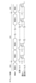
- FIG. 6 shows a timing chart relating to distance measurement operations during one frame period of pixels according to the first embodiment.
- reset signal V RST PD bias control signal V D
- gate voltage V EG of charge emission source transistor 342 charge control signal V R
- charge charge signal V I charge voltage of second capacitor 343 are shown in order from the top.
- the drive signal for the light source 1 is generated by the vertical drive circuit 24 that receives the signal from the timing signal generator 4 .
- the cathode terminal of the light receiving element 31 receives the PD bias control signal VD received at the source of the reset transistor 32, and the voltage generated by the difference from a predetermined voltage input to the anode terminal is the breakdown voltage. is assumed to be biased in the Geiger mode, exceeding about 1V.
- the reset signal VRST becomes high level (H), and the reset transistor 32 is turned on.
- the PD bias control signal VD becomes low level (L)
- the voltage of the cathode terminal of the light receiving element 31 and the gate voltage of the inverting amplifier transistor 331 become low level.
- the inversion amplifier transistor 331 (inverter) outputs a high level voltage to the gate of the charge emission source transistor 342 .
- the charge emission source transistor 342 is turned on.
- the charge control signal VR and the charge charge signal VI become high level.
- the charging transistor 341 is turned on, and the first capacitor 37 and the second capacitor 343 are charged to high level (H').
- the first capacitor 37 and the second capacitor 343 are charged to a voltage about 0.5 to 1.0 V higher than the middle level of the charge charging signal VI set after time t1.
- the PD bias control signal VD becomes high level, and the voltage of the cathode terminal of the light receiving element 31 and the gate voltage of the inverting amplifier transistor 331 become high level. This enables the light receiving element 31 to receive light.
- the inversion amplifier transistor 331 (inverter) outputs a low-level voltage to the gate of the charge emission source transistor 342, so that the charge emission source transistor 342 is turned off. Therefore, the first capacitor 37 maintains a high level voltage until the photodetector 31 detects photons.
- the charge charging signal VI becomes middle level (M), which is an intermediate voltage, and the second capacitor 343 is charged to the middle level.
- the reset signal VRST becomes high level, and the reset transistor 32 is turned on.
- a high level voltage is applied to the cathode terminal of the light receiving element 31, so that a voltage higher than the break voltage is applied between the cathode terminal and the anode terminal of the light receiving element 31, and exposure is started. be.
- the exposure period is from time t3 to t10.
- the light receiving element 31 detects one photon just before times t4, t6, and t8. At times t4, t6, and t8, the light receiving element 31 receives one photon, generates a Geiger mode pulse, and further performs self-quenching and self-recovery to output a rectangular signal shown in FIG. 5(b). do. Then, the inverting amplifier transistor 331 (inverter) outputs a rectangular pulse (FIG. 5(c)) of a constant time ⁇ T according to the equation (6).
- the gate voltage VEG becomes high level for a certain period of time .DELTA.T, and the charge emission source transistor 342 is turned on for a certain period of time .DELTA.T.
- the charge emission source transistor 342 emits electrons from the second capacitor 343 to the first capacitor 37 during each of the periods t4-t5, t6-t7, and t8-t9 according to equation (5). Therefore, the charging voltage VCF of the second capacitor 343 gradually increases, and the charging voltage VCM of the first capacitor gradually decreases.
- the change in voltage in each period t4-t5, t6-t7, t8-t9 changes logarithmically (non-linearly) with respect to the number of photons as shown in equation (5).
- the reset signal VRST and the PD bias control signal VD go low, ending the exposure period. Then, it shifts to the readout period, and after the readout of all the pixels is completed, it shifts to the next frame.
- FIG. 7 is a block diagram showing an example of the overall configuration of a distance measuring device according to the second embodiment.
- the distance measuring device according to this embodiment includes a light source 1, a light receiving sensor 2, a signal processing device 3, and a timing signal generator 4.
- the imaging element (light receiving sensor 2) of the first embodiment is used for the light receiving sensor 2.
- the light receiving sensor 2 receives the light emitted by the light source 1 and reflected by the subject.
- the light receiving sensor 2 outputs an output signal indicating the light receiving result to the signal processing device 3 .
- the signal processing device 3 calculates the distance to the subject based on the signal received from the light receiving sensor 2.
- the signal processing device 3 outputs a signal indicating the calculation result.
- the timing signal generator 4 outputs to the light source 1, the light receiving sensor 2, and the signal processing device 3 signals indicating their drive timings. Specifically, the timing signal generator 4 generates a signal whose phase is synchronized with the frame rate of the light receiving sensor 2 so that the light source 1, the light receiving sensor 2, and the signal processing device 3 perform an all-pixel simultaneous imaging (global shutter) operation. to output The frequencies of the signals output by the timing signal generator 4 may be different from each other.
- FIG. 8 is a diagram for explaining the principle of distance measurement by the distance measuring device according to the second embodiment.
- the distance measuring device according to the second embodiment can generate sub-range (SR) images SR1-SR5 and a full-range (FR) image FR1 composed of sub-range images SR1-SR5.
- SR sub-range
- FR full-range
- the flight time (the time from when the light is emitted from the light source 1 until it is reflected by the subject and returns to the light receiving sensor 2) varies depending on the distance from the light source 1 to the subject.
- the exposure time of the light receiving sensor 2 By setting the exposure time of the light receiving sensor 2 based on the time of flight, it is possible to detect a subject at a predetermined distance.
- the exposure time in each subrange is the distance corresponding to the central position between the light source and the preceding and succeeding subranges (for example, subrange images SR2 and SR4 in the case of subrange image SR3).
- the timing is set to be delayed by the round-trip flight time.
- the photon count value at the position corresponding to each subrange can be obtained.
- the light receiving sensor 2 determines that there is an object when the count value exceeds a certain threshold, and outputs a signal of a predetermined output level to generate an image of the subrange. Further, the light receiving sensor 2 generates a full-range image FR1 by superimposing a plurality of obtained sub-range images (sub-range images SR1 to SR5 in FIG. 8).
- FIG. 9 is a diagram for explaining a subrange image generation method according to the second embodiment.
- FIG. 9 shows the generation timing of the sub-range image SR3.
- the light-receiving sensor 2 performs exposure during the period when the exposure+exposure end pulse is high.
- the light-receiving sensor 2 performs this exposure operation a plurality of times (n times in this embodiment) to create the sub-range image SR3, and counts the number of photons reflected back from the subject.
- the amount of reflected light from the subject is large, so a larger number of photons (typically 20 or more) are counted. There must be.
- the amount of reflected light from the subject is small, so the number of photons required for counting may be small (typically 2 the following).
- FIG. 10 shows a timing chart regarding distance measurement operations during one frame period of pixels according to the second embodiment.
- the imaging element (light receiving sensor 2) of FIG. 5 and the pixel 30 of Fig.4 (a) are used.
- the timing signal generator 4 inputs the light emission signal indicating the light emission timing of the light source 1 to the sensor timing generator 25 .
- the sensor timing generator 25 outputs each signal according to the light emission signal.
- the amount of reflected light from the subject is large. (Decrease current source mode).
- time t0 to time t2 The operation from time t0 to time t2 is the same as in FIG.
- exposure is started after a delay time ( ⁇ 3 in the subrange image SR3) corresponding to the flight distance to the center of each subrange.
- a delay time ⁇ 3 in the subrange image SR3
- exposure starts at times t3, t6 and t9, and ends at times t5, t8 and t10.
- These exposure cycles are the same as the light emission cycle of the light source 1 .
- the exposure end time at this time is set so that the exposure period is a time ⁇ T' longer than the charge discharge time ⁇ T determined by Equation (6). That is, the exposure time of the charge emission source transistor 342 is set in consideration of the quenching time when photons are detected in the latter half of the exposure period.
- the charge emission source transistor 342 operates in constant current mode by constantly applying a fixed bias voltage to the source. As a result, it is possible to count a small number of photons while maintaining the linearity of the charge capacity.
- the distance measuring apparatus switches the charge emission source transistor 342 between the decreasing current source mode and the constant current mode according to the number of photons to be detected from short distance to long distance. Since it can be switched to the source mode, high-precision ranging is realized by photon counting with a high dynamic range.
Landscapes
- Engineering & Computer Science (AREA)
- Physics & Mathematics (AREA)
- Computer Networks & Wireless Communication (AREA)
- General Physics & Mathematics (AREA)
- Radar, Positioning & Navigation (AREA)
- Remote Sensing (AREA)
- Multimedia (AREA)
- Signal Processing (AREA)
- Electromagnetism (AREA)
- Optical Radar Systems And Details Thereof (AREA)
Priority Applications (3)
| Application Number | Priority Date | Filing Date | Title |
|---|---|---|---|
| CN202280071898.4A CN118160320A (zh) | 2021-11-02 | 2022-10-27 | 成像元件及测距装置 |
| JP2023557982A JP7672048B2 (ja) | 2021-11-02 | 2022-10-27 | 撮像素子および測距装置 |
| US18/650,988 US20240284072A1 (en) | 2021-11-02 | 2024-04-30 | Imaging element and ranging device |
Applications Claiming Priority (2)
| Application Number | Priority Date | Filing Date | Title |
|---|---|---|---|
| JP2021-179342 | 2021-11-02 | ||
| JP2021179342 | 2021-11-02 |
Related Child Applications (1)
| Application Number | Title | Priority Date | Filing Date |
|---|---|---|---|
| US18/650,988 Continuation US20240284072A1 (en) | 2021-11-02 | 2024-04-30 | Imaging element and ranging device |
Publications (1)
| Publication Number | Publication Date |
|---|---|
| WO2023080044A1 true WO2023080044A1 (ja) | 2023-05-11 |
Family
ID=86241042
Family Applications (1)
| Application Number | Title | Priority Date | Filing Date |
|---|---|---|---|
| PCT/JP2022/040046 Ceased WO2023080044A1 (ja) | 2021-11-02 | 2022-10-27 | 撮像素子および測距装置 |
Country Status (4)
| Country | Link |
|---|---|
| US (1) | US20240284072A1 (https=) |
| JP (1) | JP7672048B2 (https=) |
| CN (1) | CN118160320A (https=) |
| WO (1) | WO2023080044A1 (https=) |
Citations (3)
| Publication number | Priority date | Publication date | Assignee | Title |
|---|---|---|---|---|
| WO2019186838A1 (ja) * | 2018-03-28 | 2019-10-03 | パナソニックIpマネジメント株式会社 | 固体撮像素子、固体撮像装置、固体撮像システム、固体撮像素子の駆動方法 |
| JP6910010B2 (ja) * | 2016-02-17 | 2021-07-28 | パナソニックIpマネジメント株式会社 | 距離測定装置 |
| WO2021199225A1 (ja) * | 2020-03-31 | 2021-10-07 | パナソニックIpマネジメント株式会社 | 情報処理システム、センサシステム、情報処理方法、及びプログラム |
Family Cites Families (3)
| Publication number | Priority date | Publication date | Assignee | Title |
|---|---|---|---|---|
| WO2018216400A1 (ja) * | 2017-05-25 | 2018-11-29 | パナソニックIpマネジメント株式会社 | 固体撮像素子、及び撮像装置 |
| US11506765B2 (en) * | 2018-12-05 | 2022-11-22 | Sense Photonics, Inc. | Hybrid center of mass method (CMM) pixel |
| JP7281718B2 (ja) | 2019-11-29 | 2023-05-26 | パナソニックIpマネジメント株式会社 | 光検出器、固体撮像装置、及び、距離測定装置 |
-
2022
- 2022-10-27 CN CN202280071898.4A patent/CN118160320A/zh active Pending
- 2022-10-27 WO PCT/JP2022/040046 patent/WO2023080044A1/ja not_active Ceased
- 2022-10-27 JP JP2023557982A patent/JP7672048B2/ja active Active
-
2024
- 2024-04-30 US US18/650,988 patent/US20240284072A1/en active Pending
Patent Citations (3)
| Publication number | Priority date | Publication date | Assignee | Title |
|---|---|---|---|---|
| JP6910010B2 (ja) * | 2016-02-17 | 2021-07-28 | パナソニックIpマネジメント株式会社 | 距離測定装置 |
| WO2019186838A1 (ja) * | 2018-03-28 | 2019-10-03 | パナソニックIpマネジメント株式会社 | 固体撮像素子、固体撮像装置、固体撮像システム、固体撮像素子の駆動方法 |
| WO2021199225A1 (ja) * | 2020-03-31 | 2021-10-07 | パナソニックIpマネジメント株式会社 | 情報処理システム、センサシステム、情報処理方法、及びプログラム |
Also Published As
| Publication number | Publication date |
|---|---|
| US20240284072A1 (en) | 2024-08-22 |
| CN118160320A (zh) | 2024-06-07 |
| JP7672048B2 (ja) | 2025-05-07 |
| JPWO2023080044A1 (https=) | 2023-05-11 |
Similar Documents
| Publication | Publication Date | Title |
|---|---|---|
| US10812729B2 (en) | Solid-state imaging device | |
| US10498991B2 (en) | High dynamic range pixel and a method for operating it | |
| US10838066B2 (en) | Solid-state imaging device, distance measurement device, and distance measurement method | |
| US11405577B2 (en) | Distance image measurement device and distance image measurement method | |
| US11159738B2 (en) | Imaging devices with single-photon avalanche diodes having sub-exposures for high dynamic range | |
| US8716643B2 (en) | Single photon counting image sensor and method | |
| TW202112122A (zh) | 距離影像攝像裝置及距離影像攝像方法 | |
| JP7043218B2 (ja) | 光センサ、距離測定装置、および電子機器 | |
| US20180259625A1 (en) | LiDAR Readout Circuit | |
| US8338773B2 (en) | High-speed analog photon counter and method | |
| JP2008542706A (ja) | 光子計数装置 | |
| JP6735515B2 (ja) | 固体撮像装置 | |
| CN111048540B (zh) | 一种门控式像素单元以及3d图像传感器 | |
| US20200408910A1 (en) | Distance measuring method and distance measuring device | |
| JP7672048B2 (ja) | 撮像素子および測距装置 | |
| JP7689346B2 (ja) | 撮像素子および測距装置 | |
| US11553150B2 (en) | In pixel time amplifier for LIDAR applications | |
| US11768106B2 (en) | Photoelectric conversion device for counting a pulse signal and measuring a time when a count value is output | |
| US20250220323A1 (en) | Solid-state imaging device | |
| JP5275911B2 (ja) | 信号処理装置および光検出装置 | |
| JP2022191793A (ja) | 距離画像撮像装置及び距離画像撮像方法 |
Legal Events
| Date | Code | Title | Description |
|---|---|---|---|
| 121 | Ep: the epo has been informed by wipo that ep was designated in this application |
Ref document number: 22889864 Country of ref document: EP Kind code of ref document: A1 |
|
| WWE | Wipo information: entry into national phase |
Ref document number: 2023557982 Country of ref document: JP |
|
| WWE | Wipo information: entry into national phase |
Ref document number: 202280071898.4 Country of ref document: CN |
|
| NENP | Non-entry into the national phase |
Ref country code: DE |
|
| 122 | Ep: pct application non-entry in european phase |
Ref document number: 22889864 Country of ref document: EP Kind code of ref document: A1 |