WO2023079896A1 - Acceleration detection device - Google Patents
Acceleration detection device Download PDFInfo
- Publication number
- WO2023079896A1 WO2023079896A1 PCT/JP2022/037390 JP2022037390W WO2023079896A1 WO 2023079896 A1 WO2023079896 A1 WO 2023079896A1 JP 2022037390 W JP2022037390 W JP 2022037390W WO 2023079896 A1 WO2023079896 A1 WO 2023079896A1
- Authority
- WO
- WIPO (PCT)
- Prior art keywords
- substrate
- acceleration detection
- rigidity
- detection device
- view
- Prior art date
Links
Images


Classifications
-
- G—PHYSICS
- G01—MEASURING; TESTING
- G01P—MEASURING LINEAR OR ANGULAR SPEED, ACCELERATION, DECELERATION, OR SHOCK; INDICATING PRESENCE, ABSENCE, OR DIRECTION, OF MOVEMENT
- G01P15/00—Measuring acceleration; Measuring deceleration; Measuring shock, i.e. sudden change of acceleration
- G01P15/02—Measuring acceleration; Measuring deceleration; Measuring shock, i.e. sudden change of acceleration by making use of inertia forces using solid seismic masses
- G01P15/08—Measuring acceleration; Measuring deceleration; Measuring shock, i.e. sudden change of acceleration by making use of inertia forces using solid seismic masses with conversion into electric or magnetic values
Definitions
- the present invention relates to an acceleration detection device for detecting vibration of an object.
- Japanese Unexamined Patent Application Publication No. 2002-200002 discloses an acceleration detection device that detects the acceleration of a vehicle.
- an acceleration detection element and circuit components are mounted on one surface of a substrate. The other surface of the substrate is fixed to the object to be detected.
- the sensor section is arranged in a housing composed of a wiring board and a lid.
- the housing is arranged on the circuit board with a space therebetween.
- the housing is supported on the circuit board by a housing support made of a low-rigidity material.
- a space between the housing and the circuit board is connected to the external environment via an orifice or the like. This is intended to improve vibration resistance.
- JP 2011-75442 A Japanese Patent Application Laid-Open No. 2011-38908
- An object of the present invention is to provide an acceleration detection device that can be miniaturized and capable of detecting high-frequency acceleration with high precision.
- An acceleration detection device includes a substrate including a first main surface and a second main surface facing each other; an acceleration detection element mounted on the first main surface of the substrate; A circuit component mounted on at least the second main surface of the first main surface and the second main surface of the substrate, and the acceleration detection element provided on the first main surface of the substrate.
- an acceleration detection device that can be miniaturized and that can detect high-frequency acceleration with high precision.
- FIG. 1 is a schematic perspective view for explaining an acceleration detection device according to a first embodiment of the invention.
- FIG. 2 is a schematic perspective view of the acceleration detection device according to the first embodiment of the present invention, viewed from the second main surface side of the substrate.
- FIG. 3 is a schematic cross-sectional view along line II in FIG.
- FIG. 4 is a schematic plan view showing the positional relationship between the substrate and the high-rigidity member in the first embodiment of the present invention.
- FIG. 5 is a schematic front sectional view of the acceleration detection device of the first comparative example.
- FIG. 6 is a schematic front cross-sectional view of an acceleration detection device of a second comparative example.
- FIG. 1 is a schematic perspective view for explaining an acceleration detection device according to a first embodiment of the invention.
- FIG. 2 is a schematic perspective view of the acceleration detection device according to the first embodiment of the present invention, viewed from the second main surface side of the substrate.
- FIG. 3 is a schematic cross-sectional view along line
- FIG. 7 is a diagram showing the relationship between frequency and acceleration for explaining the range of frequencies in which acceleration can be detected in the first embodiment, first comparative example, and second comparative example of the present invention; is.
- FIG. 8 is a schematic plan view for explaining an example of four regions in the first embodiment of the invention.
- FIG. 9 is a schematic plan view showing the positional relationship between the substrate and the high-rigidity member in the modification of the first embodiment of the present invention.
- FIG. 10 is a diagram showing the relationship between the total installation area of a plurality of high-rigidity members, the number of high-rigidity members, and the resonance frequency of the entire structure of the acceleration detection device.
- FIG. 8 is a schematic plan view for explaining an example of four regions in the first embodiment of the invention.
- FIG. 9 is a schematic plan view showing the positional relationship between the substrate and the high-rigidity member in the modification of the first embodiment of the present invention.
- FIG. 10 is a diagram showing the relationship between the total installation area of
- FIG. 11 is a schematic plan view showing the positional relationship between the substrate and the high-rigidity member in the second embodiment of the present invention.
- FIG. 12 is a schematic plan view showing the positional relationship between the substrate and the high-rigidity member in the third embodiment of the invention.
- FIG. 13 is a schematic plan view showing the positional relationship between the substrate and the high-rigidity member in the fourth embodiment of the invention.
- FIG. 14 is a schematic front sectional view of an acceleration detection device according to a fourth embodiment of the invention.
- FIG. 15 is a perspective view of an example of an acceleration detection element.
- FIG. 16 is a perspective view for explaining the internal structure of one example of the acceleration detection element.
- FIG. 17 is a perspective view of an example of an acceleration detection element.
- FIG. 18 is a perspective view for explaining the internal structure of one example of the acceleration detection element.
- FIG. 19 is a schematic perspective view for explaining an acceleration detection device according to a fifth embodiment of the invention.
- FIG. 1 is a schematic perspective view for explaining the acceleration detection device according to the first embodiment of the present invention.
- FIG. 2 is a schematic perspective view of the acceleration detection device according to the first embodiment, viewed from the second main surface side of the substrate.
- FIG. 3 is a schematic cross-sectional view along line II in FIG. In FIG. 3, each element is shown schematically by adding two diagonal lines to a rectangle.
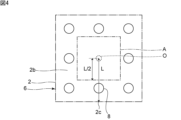
- the acceleration detection device 1 has a substrate 2 as shown in FIGS.
- the shape of the substrate 2 is square in plan view.
- the shape of the substrate 2 in plan view is not limited to the above, and may be, for example, a rectangle or another polygon.
- planar view refers to a direction viewed from above in FIG.
- the substrate 2 has a first main surface 2a and a second main surface 2b.
- the first main surface 2a and the second main surface 2b face each other.
- the substrate 2 is made of, for example, an insulating material such as glass epoxy or alumina.
- the first main surface 2a and the second main surface 2b of the substrate 2 are provided with wiring and the like for electrical connection.
- the acceleration detection device 1 has an acceleration detection element 3, a plurality of circuit components, and a plurality of high-rigidity members 8.
- the multiple circuit components include multiple first circuit components 4 and multiple second circuit components 5 .
- the acceleration detection element 3 is mounted on the first principal surface 2 a of the substrate 2 .
- the acceleration detection element 3 is an element that detects acceleration applied to the acceleration detection device 1 .
- the acceleration detection element 3 outputs an electrical signal corresponding to the magnitude of the applied acceleration.
- a plurality of first circuit components 4 are mounted on the first main surface 2 a of the substrate 2 .
- a plurality of second circuit components 5 are mounted on the second main surface 2b.
- the first circuit component 4 and the second circuit component 5 are electrically connected to each other.
- the first circuit component 4 and the second circuit component 5 constitute an electric circuit for driving the acceleration detection element 3 and for outputting signals from the acceleration detection element 3 .
- the circuit component should just be provided in the 2nd main surface 2b at least among the 1st main surface 2a and the 2nd main surface 2b.
- a main body 6 of the acceleration detection device 1 is composed of the board 2 , the acceleration detection element 3 , the plurality of first circuit components 4 and the plurality of second circuit components 5 .
- the acceleration detection element 3 is positioned at the center of the first main surface 2a of the substrate 2.
- the center of gravity of the body portion 6 is positioned at the center of the substrate 2 .
- the positions of the acceleration detecting element 3, each first circuit component 4 and each second circuit component 5 are not particularly limited.
- the position of the center of gravity of the body portion 6 is not limited to the above either.
- the acceleration detection device 1 has a sealing member 10.
- the sealing member 10 is made of resin.
- the sealing member 10 has a first sealing portion 11 and a second sealing portion 12 .
- the first sealing portion 11 is provided on the first main surface 2 a of the substrate 2 .
- the first sealing portion 11 covers the acceleration detection element 3 and the plurality of first circuit components 4 .
- the second sealing portion 12 is provided on the second main surface 2b.
- the second sealing portion 12 covers the plurality of second circuit components 5 .
- a sealing member 10 seals the acceleration detection element 3 , the plurality of first circuit components 4 , and the plurality of second circuit components 5 in the acceleration detection device 1 .
- the second sealing portion 12 has a first surface 12a and a second surface 12b.
- the first surface 12a and the second surface 12b face each other.
- First surface 12 a faces second main surface 2 b of substrate 2 .
- the second surface 12b is a surface located outside the acceleration detection device 1.
- the second surface 12b is fixed to the detection object 13 of the acceleration detection device 1.
- the second surface 12b is the mounting surface of the acceleration detection device 1. As shown in FIG.
- thermosetting resin such as epoxy resin, silicone resin or polyurethane resin, or thermoplastic resin such as acrylic resin or polyethylene resin can be used.
- a plurality of high-rigidity members 8 are provided inside the second sealing portion 12 of the sealing member 10 .
- a plurality of high-rigidity members 8 extend in a direction connecting the second surface 12 b of the second sealing portion 12 and the second main surface 2 b of the substrate 2 .
- the high-rigidity member 8 is made of a material having higher rigidity than the sealing member 10 .
- the high-rigidity member 8 consists of a cylindrical metal pin.
- the high-rigidity member 8 is not limited to a columnar shape, and may be a columnar body of any shape.
- the metal material of the high-rigidity member 8 for example, at least one metal selected from the group consisting of iron, aluminum, nickel, and alloys mainly composed of these can be used. However, appropriate ceramics can also be used as the material of the high-rigidity member 8 . At least one high-rigidity member 8 may be provided.
- FIG. 4 is a schematic plan view showing the positional relationship between the substrate and the high-rigidity member in the first embodiment.
- components other than the substrate 2 and the high-rigidity member 8 are omitted. The same applies to other schematic plan views.
- eight high-rigidity members 8 are provided.
- the plurality of high-rigidity members 8 are positioned outside the center of gravity O of the main body 6 in plan view. More specifically, the multiple high-rigidity members 8 surround the center of gravity O in plan view.
- each of the plurality of high-rigidity members 8 is joined to the second main surface 2b of the substrate 2 with a conductive joining material 9a.
- the plurality of high-rigidity members 8 electrically connect the wiring provided on the substrate 2, the acceleration detecting element 3, the plurality of first circuit components 4, and the plurality of second circuit components 5 through the conductive bonding material 9a. properly connected.
- the plurality of high-rigidity members 8 may not necessarily be electrically connected to the acceleration detection element 3, the plurality of first circuit components 4, and the plurality of second circuit components 5.
- An appropriate conductive bonding material such as solder or a conductive adhesive can be used for the conductive bonding material 9a.
- An insulating bonding material may be used instead of the conductive bonding material 9a.
- the ends of the plurality of high-rigidity members 8 farther from the substrate 2 are joined to the mounting surface 13a of the detection object 13 via the joining material 9b.
- the acceleration detection device 1 is fixed to the detection object 13 .
- the bonding material 9b may be a conductive bonding material or a non-conductive bonding material.
- a first feature of the acceleration detection device 1 is that the acceleration detection element 3 is mounted on the first main surface 2a of the substrate 2, and the second circuit component 5 is mounted on the second main surface 2b of the substrate 2. There is As a result, the area of the portion of the substrate 2 where the circuit components are provided can be reduced, and the acceleration detection device 1 can be miniaturized. In addition, it is preferable that circuit components are provided on both the first main surface 2a and the second main surface 2b of the substrate 2 as in the present embodiment. As a result, the acceleration detection device 1 can be made even more compact.
- a second feature of the acceleration detection device 1 is that the high-rigidity member 8 is composed of the substrate 2, the acceleration detection element 3, the first circuit component 4, and the second circuit component 5. are also located outside in plan view. As a result, vibration in the acceleration detection device 1 can be suppressed, and high-frequency acceleration can be detected with high accuracy. This will be described below with reference to a first comparative example and a second comparative example in addition to the present embodiment.
- a first comparative example shown in FIG. 5 differs from the first embodiment in that it does not have a high-rigidity member 8 .
- the second comparative example shown in FIG. 6 differs from the first embodiment in that there is one high-rigidity member 8 and that the high-rigidity member 8 overlaps the center of gravity of the main body 6 in plan view. .
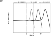
- FIG. 7 is a diagram showing the relationship between frequency and acceleration for explaining the frequency range over which acceleration can be detected in the first embodiment, first comparative example, and second comparative example.
- the acceleration applied to the element does not substantially depend on the frequency at frequencies lower than the frequency indicated by the two-dot chain line D.
- the acceleration depends on the frequency. Therefore, at frequencies higher than the two-dot chain line D, the detected acceleration is affected by the frequency, and the accuracy of detection is lowered. Therefore, in the first embodiment, acceleration can be detected with high accuracy in a frequency range lower than the frequency indicated by the two-dot chain line D.
- acceleration can be preferably detected in a frequency range lower than the frequency indicated by the two-dot chain line E.
- acceleration can be preferably detected in a frequency range lower than the frequency indicated by the two-dot chain line F.
- the frequency indicated by the two-dot chain line D is higher than the frequencies indicated by the two-dot chain lines E and F. Therefore, it can be seen that in the first embodiment, acceleration can be detected with high accuracy at frequencies higher than those in the first and second comparative examples. The reason for this will be explained below.
- the acceleration applied to the element has a maximum value at frequencies higher than the two-dot chain line E. This is because the entire structure of the acceleration detection device resonates.
- the frequency at which the acceleration has a maximum value in FIG. 7 schematically shows the resonance frequency of the entire structure of the acceleration detection device when the acceleration detection device is fixed to the detection object 13 .
- the acceleration detection device is fixed to the detection object 13 by the sealing member 10 . Since the sealing member 10 is made of resin, it has low rigidity. Furthermore, as indicated by arrow B, the entire structure of the acceleration detection device easily vibrates in directions substantially parallel to the first main surface 2 a and the second main surface 2 b of the substrate 2 . Therefore, in the first comparative example, the resonance frequency of the entire structure of the acceleration detection device is low.
- a high-rigidity member 8 is provided in the second comparative example. Therefore, the resonance frequency of the entire structure of the acceleration detection device is increased. However, as indicated by arrow C, suppression of vibration in the direction substantially parallel to the first main surface 2a and the second main surface 2b of the substrate 2 is insufficient. Therefore, although the resonance frequency of the entire structure of the acceleration detection device in the second comparative example is higher than that in the first comparative example, it is not sufficiently high.
- the plurality of high-rigidity members 8 are positioned outside the center of gravity of the main body 6 in plan view.
- the entire acceleration detection device 1 can be favorably supported by the high-rigidity member 8 .
- the vibration in the direction substantially parallel to the first main surface 2a and the second main surface 2b of the substrate 2 can be suppressed.
- the rigidity of the high-rigidity member 8 is higher than that of the sealing member 10 . Therefore, the resonance frequency of the entire structure of the acceleration detection device 1 can be effectively increased, and high-frequency acceleration can be detected with high accuracy.
- the plurality of high-rigidity members 8 be positioned on the outer peripheral side of the substrate 2 . More specifically, the plurality of high-rigidity members 8 are located outside the area indicated by the two-dot chain line A in FIG. When the distance between the center of gravity O of the main body 6 and the outer peripheral edge of the substrate 2 is L, the two-dot chain line A is a line connecting the points at a distance of 1/2 of the distance L.
- the outer peripheral edge of the substrate 2 includes a plurality of facing portions 2c.
- the facing portion 2c is located on a straight line connecting the center of gravity O and the high-rigidity member 8, sandwiches the high-rigidity member 8 together with the center of gravity O, and faces the center of gravity O.
- the substrate 2 has eight opposing portions 2c.
- the distance between the center of gravity O and the center of the high-rigidity member 8 is 1/2 times the distance L between the center of gravity O of the body portion 6 and the facing portion 2c. It is preferable that it is above.
- the entire acceleration detection device 1 can be effectively supported by the high-rigidity member 8 .
- the vibration in the direction substantially parallel to the first main surface 2a and the second main surface 2b of the substrate 2 can be effectively suppressed. Therefore, high-frequency acceleration can be detected with even higher accuracy.
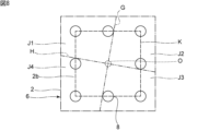
- FIG. 8 is a schematic plan view for explaining an example of four regions in the first embodiment.
- the straight lines G and H in FIG. 8 are examples, and the directions of the straight lines G and H are arbitrary.
- the straight line G and the straight line H should be orthogonal to each other.
- dashed lines K in FIG. 8 are lines connecting the centers of the plurality of high-rigidity members 8 .
- first region J1 in a plan view, four regions bounded by two straight lines G and H that pass through the center of gravity O of the main body 6 and are perpendicular to each other are defined as a first region J1 and a second region J1.
- the first region J1 is adjacent to the second region J2 and the fourth region J4, and is not adjacent to the third region J3.
- the high-rigidity members 8 are positioned in both the first area J1 and the third area J3.
- the plurality of high-rigidity members 8 include at least one pair of high-rigidity members 8 located in two non-adjacent regions among the four regions.
- the acceleration detection device 1 as a whole can be supported by at least one pair of high-rigidity members 8 in regions facing each other with the center of gravity O therebetween. Thereby, the vibration in the direction substantially parallel to the first main surface 2a and the second main surface 2b of the substrate 2 can be effectively suppressed.
- At least one pair of high-rigidity members 8 located in the first region J1 and the third region J3 are opposed to each other with the center of gravity O of the main body 6 interposed therebetween. Thereby, the vibration in the direction substantially parallel to the first main surface 2a and the second main surface 2b of the substrate 2 can be suppressed more effectively.
- At least one high-rigidity member 8 is positioned in each of the first region J1, the second region J2, the third region J3, and the fourth region J4, as in the first embodiment. is more preferred.
- the acceleration detection device 1 as a whole can be supported by at least one pair of high-rigidity members 8 in each of two sets of regions facing each other across the center of gravity O of the main body 6 . Thereby, the vibration in the direction substantially parallel to the first main surface 2a and the second main surface 2b of the substrate 2 can be further suppressed.
- At least one pair of high-rigidity members 8 located in the first region J1 and the third region J3 are opposed to each other with the center of gravity O of the main body 6 interposed therebetween.
- at least one pair of high-rigidity members 8 located in the second region J2 and the fourth region J4 are opposed to each other with the center of gravity O interposed therebetween.
- the straight lines G and H need only be orthogonal to each other, and the directions of the straight lines G and H are arbitrary.
- the positions of the four regions are determined by straight lines G and H in arbitrary directions.
- the positions of the above-described four regions bounded by any one of the straight lines G and H in any direction and the positions of the plurality of high-rigidity members 8 have any of the above relationships. is preferred. Note that the above four regions are established even when the shape of the substrate 2 in a plan view is other than a square. Therefore, it is preferable that the positions of the four regions and the positions of the plurality of high-rigidity members 8 have any of the above relationships regardless of the shape of the substrate 2 in plan view.
- the shape of the portion surrounded by the lines connecting the centers of the multiple high-rigidity members 8 is a square. More specifically, the shape of the portion surrounded by the lines connecting the centers of the plurality of high-rigidity members 8 with the maximum area is a square.
- the shape of the substrate 2 in plan view is also square. Thus, in plan view, the area of the portion surrounded by the line connecting the centers of the plurality of high-rigidity members 8 is maximized, and the shape of the portion surrounded by the line and the shape of the substrate 2 are similar. Having a relationship is preferred. In this case, it is easy to uniformly support the acceleration detection device 1 as a whole.
- one high-rigidity member 8 is positioned on every line connecting the center of the substrate 2 and each vertex of the substrate 2 in plan view.
- the acceleration detection device 1 as a whole can be supported more reliably and uniformly.
- the resonance frequency of the entire structure of the acceleration detection device 1 can be increased more reliably and effectively, and high-frequency acceleration can be detected with even higher accuracy.
- the shape of the substrate in plan view is a polygon other than a square, such as a rectangle
- the area of the portion surrounded by the lines connecting the centers of the multiple high-rigidity members is the largest in plan view. It is preferable that the shape of the enclosed portion and the shape of the substrate have a similar relationship. Also in this case, high-frequency acceleration can be detected with much higher accuracy.
- FIG. 9 is a schematic plan view showing the positional relationship between the substrate and the high-rigidity member in the modified example of the first embodiment.
- each high-rigidity member 8 is positioned on a diagonal line on the second main surface 2b of the substrate 2 in plan view.
- two pairs of high-rigidity members 8 face each other with the center of gravity O of the main body 6 interposed therebetween. Therefore, the vibration in the direction substantially parallel to the first main surface 2a and the second main surface 2b of the substrate 2 can be effectively suppressed, and high-frequency acceleration can be detected with high accuracy.
- the first circuit component and the second circuit component are arranged in the same manner as in the first embodiment. As a result, the acceleration detection device can be miniaturized.
- the resonance frequency was measured each time the area of each high-rigidity member 8 was changed. More specifically, the diameter of the high-rigidity member 8 in plan view was changed in steps of 0.2 mm ⁇ between 0.6 mm ⁇ and 1.2 mm ⁇ .
- the resonance frequency was measured each time the number of high-rigidity members 8 was changed without changing the area of each high-rigidity member 8 . More specifically, the number of high-rigidity members 8 was changed in units of one between four and eight.
- FIG. 10 is a diagram showing the relationship between the total installation area of a plurality of high-rigidity members, the number of high-rigidity members, and the resonance frequency of the entire structure of the acceleration detection device.
- the total installation area of the plurality of high-rigidity members 8 is the same as the total area of the plurality of high-rigidity members 8 in plan view.
- the slope of the change in resonance frequency with respect to the change in area is greater than when the area of each high-rigidity member 8 is increased.
- the resonance frequency is higher when seven high-rigidity members 8 are provided than when four high-rigidity members 8 are provided. I know it's expensive. Therefore, it is preferable to increase the number of high-rigidity members 8 rather than increasing the area of each high-rigidity member 8 . This effectively increases the resonance frequency of the entire structure of the acceleration detection device.
- each high-rigidity member 8 it becomes easier to arrange the high-rigidity member 8 near the outer periphery of the substrate 2 . More specifically, with the miniaturization of the acceleration detection device, high precision is required for the arrangement of the high-rigidity member 8 in the manufacturing process. By reducing the area of each high-rigidity member 8, it is possible to realize an acceleration detection device in which the high-rigidity member 8 is positioned near the outer periphery of the substrate 2. FIG. In addition, by increasing the number of high-rigidity members 8, it is possible to increase the logarithm of the high-rigidity members 8 provided in non-adjacent regions in the four regions shown in FIG. Thereby, the resonance frequency can be effectively increased.
- the first sealing portion 11 and the second sealing portion 12 in the sealing member 10 shown in FIG. 3 are preferably made of the same resin. Manufacturing can thereby be facilitated. However, the first sealing portion 11 and the second sealing portion 12 may be made of different resins. Note that the first sealing portion 11 and the second sealing portion 12 may be connected and integrated via the side surface of the substrate 2 . That is, the substrate 2 may be embedded within the sealing member 10 .
- the end of the high-rigidity member 8 farther from the substrate 2 is exposed to the outside of the sealing member 10 .
- the end portion of the high-rigidity member 8 is located inside the second sealing portion 12 relative to the second surface 12 b of the second sealing portion 12 .
- a step is provided between the second surface 12b and the end of the high-rigidity member 8. As shown in FIG. However, a step need not be provided between the second surface 12b and the end of the high-rigidity member 8 .
- the second sealing portion 12 of the sealing member 10 is not in contact with the object 13 to be detected.
- the second sealing portion 12 may be in contact with the detection target 13 when the acceleration detection device 1 is bonded to the detection target 13 .
- the detection target 13 is not particularly limited.
- the acceleration detection device of the present invention can be mounted on various objects to be detected, such as machine tools and vehicles.
- the acceleration detection device 1 may be fixed to the detection target 13 via a relay substrate made of an insulating material such as glass epoxy or alumina.
- FIG. 11 is a schematic plan view showing the positional relationship between the substrate and the high-rigidity member in the second embodiment.
- This embodiment is the first in that the shape of each high-rigidity member 28 is a quadrangular prism, and that a part of the outer periphery of each high-rigidity member 28 overlaps the outer periphery of the substrate 2 in plan view. Different from the embodiment. Except for the above points, the acceleration detection device of this embodiment has the same configuration as the acceleration detection device 1 of the first embodiment.
- the plurality of high-rigidity members 28 are located outside the center of gravity O of the main body 6 in plan view. Further, a part of the outer peripheral edge of each high-rigidity member 28 overlaps the outer peripheral edge of the substrate 2 in plan view. Thereby, the entire structure of the acceleration detection device can be effectively supported by the high-rigidity member 28 . Furthermore, although not shown, the first circuit component and the second circuit component are arranged in the same manner as in the first embodiment. Therefore, the acceleration detection device can be miniaturized, and high-frequency acceleration can be detected with even higher accuracy.
- outer peripheral edge of the high-rigidity member 28 does not have to overlap the outer peripheral edge of the substrate 2 in plan view.
- the shape of the high-rigidity member 28 in plan view is square. However, the shape of the high-rigidity member 28 in plan view may be rectangular. In these cases, the high-rigidity member 28 has a linear portion in plan view. As a result, even if the acceleration detection device is small, the high-rigidity member 28 can be arranged in the vicinity of the outer peripheral edge of the substrate 2 more reliably. Therefore, the resonance frequency of the entire structure of the acceleration detection device can be increased more reliably and effectively, and high-frequency acceleration can be detected with even higher accuracy.
- FIG. 12 is a schematic plan view showing the positional relationship between the substrate and the high-rigidity member in the third embodiment.
- the shape of the high-rigidity member 38 is frame-shaped, the number of the high-rigidity member 38 is one, and the entire outer peripheral edge of the high-rigidity member 38 is the outer peripheral edge of the substrate 2 in plan view. It differs from the first embodiment in that it overlaps. Except for the above points, the acceleration detection device of this embodiment has the same configuration as the acceleration detection device 1 of the first embodiment.
- the high-rigidity member 38 is positioned outside the center of gravity O of the main body 6 in plan view. In plan view, the outer peripheral edge of the high-rigidity member 38 overlaps the outer peripheral edge of the substrate 2 . Thereby, the entire structure of the acceleration detection device can be effectively supported by the high-rigidity member 38 . Furthermore, although not shown, the first circuit component and the second circuit component are arranged in the same manner as in the first embodiment. Therefore, the acceleration detection device can be miniaturized, and high-frequency acceleration can be detected with even higher accuracy.
- the outer shape of the high-rigidity member 38 and the shape of the substrate 2 are congruent in plan view. In this case, it is easy to uniformly support the entire acceleration detection device. As a result, the resonance frequency of the entire structure of the acceleration detection device can be effectively increased, and high-frequency acceleration can be detected with even higher accuracy.
- the outer peripheral edge of the high-rigidity member 38 does not have to overlap the outer peripheral edge of the substrate 2 in plan view.
- the outer peripheral edge of the high-rigidity member 38 may be located inside the outer peripheral edge of the substrate 2 .
- the outer shape of the high-rigidity member 38 and the shape of the substrate 2 have a similar relationship in plan view. Also in these cases, the resonance frequency of the entire structure of the acceleration detection device can be increased.
- the shape of the substrate in plan view is a polygon such as a rectangle other than a square, it is preferable that the outline of the high-rigidity member and the shape of the substrate have a congruent or similar relationship in plan view. Also in this case, high-frequency acceleration can be detected with much higher accuracy.
- a fourth embodiment will be shown below.
- the high-rigidity member corresponding to the high-rigidity members in the first to third embodiments and modifications is assumed to be the first high-rigidity member.
- FIG. 13 is a schematic plan view showing the positional relationship between the substrate and the high-rigidity member in the fourth embodiment.
- FIG. 14 is a schematic front cross-sectional view of an acceleration detection device according to a fourth embodiment.
- this embodiment differs from the third embodiment in that it has a second high-rigidity member 48B in addition to the first high-rigidity member 48A. Except for the above points, the acceleration detection device of this embodiment has the same configuration as that of the acceleration detection device of the third embodiment.
- the first high-rigidity member 48A is provided similarly to the high-rigidity member 38 as the first high-rigidity member in the third embodiment. Furthermore, as shown in FIG. 14, the first circuit component 4 and the second circuit component 5 are arranged in the same manner as in the first embodiment. Therefore, the acceleration detection device can be miniaturized, and high-frequency acceleration can be detected with even higher accuracy.
- the second high-rigidity member 48B is provided in the same manner as the high-rigidity member 8 as the first high-rigidity member in the first embodiment except for the position in plan view. More specifically, the second high-rigidity member 48B is provided in a region overlapping the acceleration detection element 3 in plan view. The second high-rigidity member 48B extends in a direction connecting the second surface 12b of the second sealing portion 12 of the sealing member 10 and the second main surface 2b of the substrate 2 .
- the second high-rigidity member 48B is made of a material having higher rigidity than the sealing member 10. As shown in FIG. In this embodiment, the second high-rigidity member 48B is a cylindrical metal pin.
- the second high-rigidity member 48B is not limited to a columnar shape, and may be a columnar body of any shape.
- the same material as that of the first high-rigidity member 48A can be used.
- the second high-rigidity member 48B is joined to the second main surface 2b of the substrate 2 with a conductive joining material 9a.
- the second high-rigidity member 48B is connected to the wiring provided on the substrate 2, the acceleration detection element 3, the plurality of first circuit components 4, and the plurality of second circuit components 5 via the conductive bonding material 9a. electrically connected.
- the second high-rigidity member 48B does not necessarily have to be electrically connected to the acceleration detection element 3, the plurality of first circuit components 4 and the plurality of second circuit components 5.
- An appropriate conductive bonding material such as solder or a conductive adhesive can be used for the conductive bonding material 9a.
- An insulating bonding material may be used instead of the conductive bonding material 9a.
- the end farther from the substrate 2 is joined to the mounting surface 13a of the detection object 13 via the joining material 9b.
- the bonding material 9b may be a conductive bonding material or a non-conductive bonding material.
- At least one second high-rigidity member 48B may be provided in a region overlapping the acceleration detection element 3 in plan view. That is, although one second high-rigidity member 48B is provided in this embodiment, a plurality of second high-rigidity members 48B may be provided.
- the acceleration detection element 3 consists of a suitable acceleration detection element that outputs an electric signal according to the magnitude of the applied acceleration. Therefore, the structure of the acceleration detecting element 3 is not particularly limited as long as it fulfills such a function, but one example will be described with reference to FIGS. 15 and 16. FIG.
- FIG. 15 is a perspective view of an example of an acceleration detection element.
- FIG. 16 is a perspective view for explaining the internal structure of one example of the acceleration detection element.
- the acceleration detection element 3 has an element substrate 51 and a cap 52.
- the cap 52 is fixed to the element substrate 51 .
- the acceleration detection element 3 has a piezoelectric element 53 for acceleration detection.
- a piezoelectric element 53 is sealed in a container constituted by the cap 52 and the element substrate 51 .
- the piezoelectric element 53 is mounted on the element substrate 51 .
- the piezoelectric element 53 has a strip-shaped elongated piezoelectric body 53a. Electrodes 53b and 53c are provided on both sides of the piezoelectric body 53a.
- the piezoelectric element 53 is a cantilever and attached to the element substrate 51 . When acceleration is applied to the piezoelectric element 53, the piezoelectric element 53 vibrates, and an electric signal is output by the piezoelectric effect.
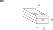
- FIG. 17 Another example of the acceleration detection element will be described with reference to FIGS. 17 and 18.
- FIG. 17 Another example of the acceleration detection element will be described with reference to FIGS. 17 and 18.
- FIG. 17 is a perspective view of an example of an acceleration detection element.
- FIG. 18 is a perspective view for explaining the internal structure of one example of the acceleration detection element.
- the acceleration detection element has a first clamping member 65, a second clamping member 66, a first exterior substrate 67, and a second exterior substrate 68.
- the acceleration sensing element has a piezoelectric element 64 .
- the piezoelectric element 64 has a rectangular parallelepiped shape.
- the piezoelectric element 64 has a first piezoelectric layer (not shown), a second piezoelectric layer, and detection electrodes.
- the first piezoelectric layer and the second piezoelectric layer are made of lead zirconate titanate-based ceramics. However, the materials of the first piezoelectric layer and the second piezoelectric layer are not limited to the above.
- the detection electrodes are provided on the outer surface of the first piezoelectric layer and the outer surface of the second piezoelectric layer, respectively.
- a first holding member 65 and a second holding member 66 are joined to the piezoelectric element 64 .
- the piezoelectric element 64 is a cantilever and is supported by a first clamping member 65 and a second clamping member 66 .
- the first holding member 65 and the second holding member 66 each have a groove that opens toward the piezoelectric element 64 .
- the groove forms a space that does not hinder displacement of the piezoelectric element 64 due to acceleration.
- the first exterior substrate 67 and the second exterior substrate 68 are made of an insulating material.
- the first exterior substrate 67 is a flat member.
- the second exterior substrate 68 has a recess.
- the recess forms a space that does not hinder displacement of the piezoelectric element 64 due to acceleration.
- the piezoelectric element 64 , the first clamping member 65 and the second clamping member 66 are arranged between the first exterior substrate 67 and the second exterior substrate 68 .
- the acceleration detection element may be an acceleration detection element having a capacitance element instead of a piezoelectric element.
- FIG. 19 shows an example in which the acceleration detection elements shown in FIGS. 17 and 18 are mounted on a substrate in a manner different from that shown in FIG. 1 and the like.
- FIG. 19 is a schematic perspective view for explaining the acceleration detection device according to the fifth embodiment of the invention.
- the acceleration detection element 63 is the acceleration detection element shown in FIGS.
- the acceleration detection element 63 is mounted near the outer periphery of the first main surface 2a of the substrate 2 . In this manner, the acceleration detection element 63 may be mounted on a portion other than the center of the substrate 2.
- FIG. A plurality of first circuit components 4 are also mounted on the first main surface 2a together with the acceleration detection element 63 .
- Acceleration detection element 63 is configured such that first holding member 65, first exterior substrate 67, and second exterior substrate 68 shown in FIG. It is mounted on the first main surface 2a. Therefore, the detection axis of the acceleration detection element 63 is perpendicular to the second surface 12 b of the second sealing portion 12 . That is, the detection axis is perpendicular to the mounting surface of the acceleration detection device 61 . For example, when the acceleration detection device 61 is mounted on a horizontal surface, the detection axis of the acceleration detection element 63 is vertical.
- a plurality of second circuit components 5 are mounted on the second main surface 2b of the substrate 2, as in the first embodiment shown in FIG. Then, as described above, the acceleration detection element 63 is mounted on the first main surface 2a. As a result, the area of the portion of the substrate 2 for providing the circuit components can be reduced, and the acceleration detection device 61 can be miniaturized.
- the main body is composed of the substrate 2, the acceleration detection element 63, the plurality of first circuit components 4, and the plurality of second circuit components.
- the acceleration detection element 63, the plurality of first circuit components 4, and the plurality of second circuit components are mounted on the substrate 2 so that the high-rigidity member 8 is located outside the center of gravity of the main body in plan view. It is As a result, as in the first embodiment, vibration in the acceleration detection device 61 can be suppressed, and high-frequency acceleration can be detected with high accuracy.
Abstract
Provided is an acceleration detection device that can be reduced in size and that can detect high-frequency acceleration with high precision. The present invention comprises: a substrate 2 having first and second main surfaces 2a, 2b; an acceleration detection element 3 mounted on the first main surface 2a; first and second circuit components 4, 5 mounted on the substrate 2; a sealing member 10 made of resin and having a first sealing part 11 that covers the acceleration detection element 3 provided on the first main surface 2a, and a second sealing part 12 that covers the second circuit component 5 provided on the second main surface 2b and that includes first and second surfaces 12a, 12b; and high-rigidity members 8 that extend, within the second sealing part 12, in a direction joining the second surface 12b and the second main surface 2b of the substrate 2, and that have a higher rigidity than that of the sealing member 10. In a plan view, the high-rigidity members 8 are positioned further to the outside than the center of gravity of a body section 6 which is constituted by the substrate 2, the acceleration detection element 3, and the first and second circuit components 4, 5.
Description
本発明は、対象物の振動等を検出するための加速度検出装置に関する。
The present invention relates to an acceleration detection device for detecting vibration of an object.
従来、加速度検出素子が搭載されている様々な加速度検出装置が知られている。例えば下記の特許文献1では、車両の加速度を検出する加速度検出装置が開示されている。特許文献1に記載の加速度検出装置では、基板の一方面に、加速度検出素子や回路部品が実装されている。基板の他方面が検出対象物に固定されている。
Conventionally, various acceleration detection devices equipped with acceleration detection elements are known. For example, Japanese Unexamined Patent Application Publication No. 2002-200002 discloses an acceleration detection device that detects the acceleration of a vehicle. In the acceleration detection device disclosed in Patent Literature 1, an acceleration detection element and circuit components are mounted on one surface of a substrate. The other surface of the substrate is fixed to the object to be detected.
他方、下記の特許文献2に記載の角速度検出装置では、センサ部は、配線基板及び蓋により構成された筐体内に配置されている。筐体は、回路基板上に、空間を隔てて配置されている。なお、筐体は、回路基板上において、低剛性材料からなる筐体支持体により支持されている。筐体及び回路基板間の空間は、オリフィスなどを介して外部環境と接続されている。これにより、耐振動性の向上が図られている。
On the other hand, in the angular velocity detection device described in Patent Document 2 below, the sensor section is arranged in a housing composed of a wiring board and a lid. The housing is arranged on the circuit board with a space therebetween. The housing is supported on the circuit board by a housing support made of a low-rigidity material. A space between the housing and the circuit board is connected to the external environment via an orifice or the like. This is intended to improve vibration resistance.
特許文献1に記載の加速度検出装置では、車両に固定される筐体に基板が固定されている。そのため、基板の筐体と対向している面に回路部品などを実装することができなかった。従って、加速度検出装置の小型化が困難であった。
In the acceleration detection device described in Patent Document 1, a substrate is fixed to a housing that is fixed to the vehicle. Therefore, it was not possible to mount circuit components or the like on the surface of the substrate facing the housing. Therefore, it has been difficult to reduce the size of the acceleration detection device.
特許文献2に記載の角速度検出装置では、筐体及び配線基板間の空間を囲む部分は、振動により変形し易く、かつ外部環境と接続されている。そのため、該空間内に回路部品を実装し、封止することはできなかった。従って、角速度検出装置の小型化が困難であった。さらに、この角速度検出装置においては、共振周波数を低くすることにより耐振動性の向上が図られているため、高周波を検知する性能は低くなる。
In the angular velocity detector described in Patent Document 2, the portion surrounding the space between the housing and the wiring board is easily deformed by vibration and is connected to the external environment. Therefore, it has not been possible to mount and seal circuit components in the space. Therefore, it has been difficult to miniaturize the angular velocity detector. Furthermore, in this angular velocity detection device, since the vibration resistance is improved by lowering the resonance frequency, the performance of detecting high frequencies is lowered.
本発明の目的は、小型化することができ、かつ高い周波数の加速度を高精度で検出することが可能である、加速度検出装置を提供することにある。
An object of the present invention is to provide an acceleration detection device that can be miniaturized and capable of detecting high-frequency acceleration with high precision.
本発明に係る加速度検出装置は、互いに対向している第1の主面及び第2の主面を含む基板と、前記基板の前記第1の主面に搭載されている加速度検出素子と、前記基板の前記第1の主面及び前記第2の主面のうち少なくとも前記第2の主面に搭載されている回路部品と、前記基板の前記第1の主面に設けられた前記加速度検出素子を覆っている第1の封止部と、前記基板の前記第2の主面に設けられた前記回路部品を覆っており、前記基板に面している第1の面、及び前記第1の面と対向している第2の面を含む第2の封止部とを有し、かつ樹脂からなる封止部材と、前記第2の封止部内において、前記第2の面と前記基板の前記第2の主面とを結ぶ方向に延びており、前記封止部材よりも剛性が高い、少なくとも1個の高剛性部材とを備え、前記高剛性部材が、前記基板、前記加速度検出素子及び前記回路部品により構成されている本体部の重心よりも、平面視において外側に位置している。
An acceleration detection device according to the present invention includes a substrate including a first main surface and a second main surface facing each other; an acceleration detection element mounted on the first main surface of the substrate; A circuit component mounted on at least the second main surface of the first main surface and the second main surface of the substrate, and the acceleration detection element provided on the first main surface of the substrate. a first surface covering the circuit component provided on the second main surface of the substrate and facing the substrate; a sealing member made of resin and having a second sealing portion including a second surface facing the second surface; and a sealing member between the second surface and the substrate in the second sealing portion at least one high-rigidity member extending in a direction connecting the second main surface and having higher rigidity than the sealing member, wherein the high-rigidity member comprises the substrate, the acceleration detection element, and the It is located outside the center of gravity of the main body constituted by the circuit parts in a plan view.
本発明によれば、小型化することができ、かつ高い周波数の加速度を高精度で検出することが可能である、加速度検出装置を提供することができる。
According to the present invention, it is possible to provide an acceleration detection device that can be miniaturized and that can detect high-frequency acceleration with high precision.
以下、図面を参照しつつ、本発明の具体的な実施形態を説明することにより、本発明を明らかにする。
Hereinafter, the present invention will be clarified by describing specific embodiments of the present invention with reference to the drawings.
なお、本明細書に記載の各実施形態は、例示的なものであり、異なる実施形態間において、構成の部分的な置換または組み合わせが可能であることを指摘しておく。
It should be noted that each embodiment described in this specification is an example, and partial replacement or combination of configurations is possible between different embodiments.
図1は、本発明の第1の実施形態に係る加速度検出装置を説明するための略図的斜視図である。図2は、第1の実施形態に係る加速度検出装置の、基板の第2の主面側から見た略図的斜視図である。図3は、図1中のI-I線に沿う略図的断面図である。図3においては、各素子を、矩形に2本の対角線を加えた略図により示す。
FIG. 1 is a schematic perspective view for explaining the acceleration detection device according to the first embodiment of the present invention. FIG. 2 is a schematic perspective view of the acceleration detection device according to the first embodiment, viewed from the second main surface side of the substrate. FIG. 3 is a schematic cross-sectional view along line II in FIG. In FIG. 3, each element is shown schematically by adding two diagonal lines to a rectangle.
図1及び図2に示すように、加速度検出装置1は基板2を有する。本実施形態においては、平面視において、基板2の形状は正方形である。もっとも、基板2の平面視における形状は上記に限定されず、例えば矩形や他の多角形などであってもよい。本明細書において、平面視とは、図3における上方から見る方向をいう。
The acceleration detection device 1 has a substrate 2 as shown in FIGS. In this embodiment, the shape of the substrate 2 is square in plan view. However, the shape of the substrate 2 in plan view is not limited to the above, and may be, for example, a rectangle or another polygon. In this specification, planar view refers to a direction viewed from above in FIG.
基板2は、第1の主面2a及び第2の主面2bを有する。第1の主面2a及び第2の主面2bは互いに対向している。基板2は、例えば、ガラスエポキシやアルミナなどの絶縁性材料からなる。図示をしていないが、基板2の第1の主面2a及び第2の主面2bには、電気的接続のための配線などが設けられている。
The substrate 2 has a first main surface 2a and a second main surface 2b. The first main surface 2a and the second main surface 2b face each other. The substrate 2 is made of, for example, an insulating material such as glass epoxy or alumina. Although not shown, the first main surface 2a and the second main surface 2b of the substrate 2 are provided with wiring and the like for electrical connection.
図3に示すように、加速度検出装置1は、加速度検出素子3と、複数の回路部品と、複数の高剛性部材8とを有する。複数の回路部品は、複数の第1の回路部品4と、複数の第2の回路部品5とを含む。加速度検出素子3は、基板2の第1の主面2aに搭載されている。加速度検出素子3は、加速度検出装置1に印加された加速度を検出する素子である。加速度検出素子3は、印加された加速度の大きさに応じた電気信号を出力する。
As shown in FIG. 3, the acceleration detection device 1 has an acceleration detection element 3, a plurality of circuit components, and a plurality of high-rigidity members 8. The multiple circuit components include multiple first circuit components 4 and multiple second circuit components 5 . The acceleration detection element 3 is mounted on the first principal surface 2 a of the substrate 2 . The acceleration detection element 3 is an element that detects acceleration applied to the acceleration detection device 1 . The acceleration detection element 3 outputs an electrical signal corresponding to the magnitude of the applied acceleration.
複数の第1の回路部品4は、基板2の第1の主面2aに搭載されている。複数の第2の回路部品5は、第2の主面2bに搭載されている。第1の回路部品4及び第2の回路部品5は、互いに電気的に接続されている。第1の回路部品4及び第2の回路部品5は、加速度検出素子3を駆動し、かつ加速度検出素子3からの信号を出力するための電気回路を構成している。なお、回路部品は、第1の主面2a及び第2の主面2bのうち少なくとも第2の主面2bに設けられていればよい。
A plurality of first circuit components 4 are mounted on the first main surface 2 a of the substrate 2 . A plurality of second circuit components 5 are mounted on the second main surface 2b. The first circuit component 4 and the second circuit component 5 are electrically connected to each other. The first circuit component 4 and the second circuit component 5 constitute an electric circuit for driving the acceleration detection element 3 and for outputting signals from the acceleration detection element 3 . In addition, the circuit component should just be provided in the 2nd main surface 2b at least among the 1st main surface 2a and the 2nd main surface 2b.
基板2、加速度検出素子3、複数の第1の回路部品4及び複数の第2の回路部品5により、加速度検出装置1の本体部6が構成されている。本実施形態においては、加速度検出素子3は、基板2の第1の主面2aの中央に位置している。本体部6の重心は、基板2の中央に位置している。もっとも、加速度検出素子3、各第1の回路部品4及び各第2の回路部品5の位置は特に限定されない。本体部6の重心の位置も上記に限定されない。
A main body 6 of the acceleration detection device 1 is composed of the board 2 , the acceleration detection element 3 , the plurality of first circuit components 4 and the plurality of second circuit components 5 . In this embodiment, the acceleration detection element 3 is positioned at the center of the first main surface 2a of the substrate 2. As shown in FIG. The center of gravity of the body portion 6 is positioned at the center of the substrate 2 . However, the positions of the acceleration detecting element 3, each first circuit component 4 and each second circuit component 5 are not particularly limited. The position of the center of gravity of the body portion 6 is not limited to the above either.
加速度検出装置1は封止部材10を有する。封止部材10は樹脂からなる。封止部材10は、第1の封止部11と、第2の封止部12とを有する。第1の封止部11は、基板2の第1の主面2aに設けられている。第1の封止部11は、加速度検出素子3及び複数の第1の回路部品4を覆っている。第2の封止部12は、第2の主面2bに設けられている。第2の封止部12は、複数の第2の回路部品5を覆っている。封止部材10によって、加速度検出装置1内の加速度検出素子3、複数の第1の回路部品4及び複数の第2の回路部品5が封止されている。
The acceleration detection device 1 has a sealing member 10. The sealing member 10 is made of resin. The sealing member 10 has a first sealing portion 11 and a second sealing portion 12 . The first sealing portion 11 is provided on the first main surface 2 a of the substrate 2 . The first sealing portion 11 covers the acceleration detection element 3 and the plurality of first circuit components 4 . The second sealing portion 12 is provided on the second main surface 2b. The second sealing portion 12 covers the plurality of second circuit components 5 . A sealing member 10 seals the acceleration detection element 3 , the plurality of first circuit components 4 , and the plurality of second circuit components 5 in the acceleration detection device 1 .
なお、第2の封止部12は、第1の面12a及び第2の面12bを有する。第1の面12a及び第2の面第12bは互いに対向している。第1の面12aは、基板2の第2の主面2bに面している。他方、第2の面12bは、加速度検出装置1における外部に位置する面である。図3に示すように、第2の面12bは、加速度検出装置1の検出対象物13に固定される。第2の面12bは加速度検出装置1における実装面である。
The second sealing portion 12 has a first surface 12a and a second surface 12b. The first surface 12a and the second surface 12b face each other. First surface 12 a faces second main surface 2 b of substrate 2 . On the other hand, the second surface 12b is a surface located outside the acceleration detection device 1. As shown in FIG. As shown in FIG. 3, the second surface 12b is fixed to the detection object 13 of the acceleration detection device 1. As shown in FIG. The second surface 12b is the mounting surface of the acceleration detection device 1. As shown in FIG.
封止部材10の樹脂材料としては、例えば、エポキシ樹脂、シリコーン樹脂またはポリウレタン樹脂などの熱硬化性樹脂や、アクリル樹脂またはポリエチレン樹脂などの熱可塑性樹脂を用いることができる。
As the resin material of the sealing member 10, for example, thermosetting resin such as epoxy resin, silicone resin or polyurethane resin, or thermoplastic resin such as acrylic resin or polyethylene resin can be used.
封止部材10の第2の封止部12内には複数の高剛性部材8が設けられている。複数の高剛性部材8は、第2の封止部12の第2の面12bと、基板2の第2の主面2bとを結ぶ方向に延びている。高剛性部材8は、封止部材10よりも剛性が高い材料からなる。本実施形態では、高剛性部材8は円柱状の金属ピンからなる。なお、高剛性部材8は円柱状に限られず、任意の形状の柱状体であってもよい。高剛性部材8の金属材料としては、例えば、鉄、アルミニウム、ニッケル及びこれらを主体とする合金からなる群から選択された少なくとも1種の金属を用いることができる。もっとも、高剛性部材8の材料としては、適宜のセラミックスを用いることもできる。高剛性部材8は少なくとも1個設けられていればよい。
A plurality of high-rigidity members 8 are provided inside the second sealing portion 12 of the sealing member 10 . A plurality of high-rigidity members 8 extend in a direction connecting the second surface 12 b of the second sealing portion 12 and the second main surface 2 b of the substrate 2 . The high-rigidity member 8 is made of a material having higher rigidity than the sealing member 10 . In this embodiment, the high-rigidity member 8 consists of a cylindrical metal pin. The high-rigidity member 8 is not limited to a columnar shape, and may be a columnar body of any shape. As the metal material of the high-rigidity member 8, for example, at least one metal selected from the group consisting of iron, aluminum, nickel, and alloys mainly composed of these can be used. However, appropriate ceramics can also be used as the material of the high-rigidity member 8 . At least one high-rigidity member 8 may be provided.
図4は、第1の実施形態における、基板及び高剛性部材の位置の関係を示す略図的平面図である。図4においては、基板2及び高剛性部材8以外を省略している。他の略図的平面図においても同様である。
FIG. 4 is a schematic plan view showing the positional relationship between the substrate and the high-rigidity member in the first embodiment. In FIG. 4, components other than the substrate 2 and the high-rigidity member 8 are omitted. The same applies to other schematic plan views.
本実施形態では、8個の高剛性部材8が設けられている。複数の高剛性部材8は、平面視において、本体部6の重心Oの外側に位置している。より具体的には、複数の高剛性部材8は、平面視において、重心Oを囲んでいる。
In this embodiment, eight high-rigidity members 8 are provided. The plurality of high-rigidity members 8 are positioned outside the center of gravity O of the main body 6 in plan view. More specifically, the multiple high-rigidity members 8 surround the center of gravity O in plan view.
図3に戻り、複数の高剛性部材8の一方端部は、導電性接合材9aにより基板2の第2の主面2bに接合されている。複数の高剛性部材8は、導電性接合材9aを介して、基板2上に設けられた配線、加速度検出素子3、複数の第1の回路部品4及び複数の第2の回路部品5に電気的に接続されている。なお、複数の高剛性部材8は、必ずしも加速度検出素子3、複数の第1の回路部品4及び複数の第2の回路部品5に電気的に接続されていなくともよい。導電性接合材9aには、半田や導電性接着剤などの適宜の導電性接合材料を用いることができる。なお、導電性接合材9aに代えて、絶縁性接合材を用いてもよい。
Returning to FIG. 3, one end of each of the plurality of high-rigidity members 8 is joined to the second main surface 2b of the substrate 2 with a conductive joining material 9a. The plurality of high-rigidity members 8 electrically connect the wiring provided on the substrate 2, the acceleration detecting element 3, the plurality of first circuit components 4, and the plurality of second circuit components 5 through the conductive bonding material 9a. properly connected. Note that the plurality of high-rigidity members 8 may not necessarily be electrically connected to the acceleration detection element 3, the plurality of first circuit components 4, and the plurality of second circuit components 5. FIG. An appropriate conductive bonding material such as solder or a conductive adhesive can be used for the conductive bonding material 9a. An insulating bonding material may be used instead of the conductive bonding material 9a.
本実施形態では、複数の高剛性部材8の両端部のうち基板2から遠い方の端部は、検出対象物13の取り付け面13aに、接合材9bを介して接合されている。それによって、加速度検出装置1が、検出対象物13に固定されている。接合材9bは、導電性接合材であってもよく、導電性を有しない接合材であってもよい。
In the present embodiment, the ends of the plurality of high-rigidity members 8 farther from the substrate 2 are joined to the mounting surface 13a of the detection object 13 via the joining material 9b. Thereby, the acceleration detection device 1 is fixed to the detection object 13 . The bonding material 9b may be a conductive bonding material or a non-conductive bonding material.
加速度検出装置1の第1の特徴は、加速度検出素子3が基板2の第1の主面2aに搭載されており、第2の回路部品5が基板2の第2の主面2bに搭載されていることにある。それによって、基板2において回路部品を設けるための部分の面積を小さくすることができ、加速度検出装置1を小型化することができる。なお、本実施形態のように、基板2の第1の主面2a及び第2の主面2bの双方に回路部品が設けられていることが好ましい。それによって、加速度検出装置1をより一層小型にすることができる。
A first feature of the acceleration detection device 1 is that the acceleration detection element 3 is mounted on the first main surface 2a of the substrate 2, and the second circuit component 5 is mounted on the second main surface 2b of the substrate 2. There is As a result, the area of the portion of the substrate 2 where the circuit components are provided can be reduced, and the acceleration detection device 1 can be miniaturized. In addition, it is preferable that circuit components are provided on both the first main surface 2a and the second main surface 2b of the substrate 2 as in the present embodiment. As a result, the acceleration detection device 1 can be made even more compact.
加速度検出装置1の第2の特徴は、高剛性部材8が、基板2、加速度検出素子3、第1の回路部品4及び第2の回路部品5により構成されている本体部6の重心Oよりも、平面視において外側に位置していることにある。それによって、加速度検出装置1における振動を抑制することができ、高い周波数の加速度を高精度で検出することができる。これを、本実施形態に加えて第1の比較例及び第2の比較例を参照し、以下において説明する。
A second feature of the acceleration detection device 1 is that the high-rigidity member 8 is composed of the substrate 2, the acceleration detection element 3, the first circuit component 4, and the second circuit component 5. are also located outside in plan view. As a result, vibration in the acceleration detection device 1 can be suppressed, and high-frequency acceleration can be detected with high accuracy. This will be described below with reference to a first comparative example and a second comparative example in addition to the present embodiment.
図5に示す第1の比較例は、高剛性部材8を有しない点において第1の実施形態と異なる。図6に示す第2の比較例は、高剛性部材8が1個であり、かつ高剛性部材8が平面視において、本体部6の重心と重なっている点において、第1の実施形態と異なる。
A first comparative example shown in FIG. 5 differs from the first embodiment in that it does not have a high-rigidity member 8 . The second comparative example shown in FIG. 6 differs from the first embodiment in that there is one high-rigidity member 8 and that the high-rigidity member 8 overlaps the center of gravity of the main body 6 in plan view. .
図7は、第1の実施形態、第1の比較例及び第2の比較例において、加速度を検出することができる周波数の範囲を説明するための、周波数及び加速度の関係を示す図である。
FIG. 7 is a diagram showing the relationship between frequency and acceleration for explaining the frequency range over which acceleration can be detected in the first embodiment, first comparative example, and second comparative example.
図7に示すように、第1の実施形態においては、二点鎖線Dに示す周波数よりも低い周波数においては、素子に加わる加速度は周波数にほぼ依存していない。一方で、二点鎖線Dに示す周波数よりも高い周波数においては、加速度が周波数に依存している。そのため、二点鎖線Dよりも高い周波数においては、検出する加速度が周波数に影響され、検出の精度が低くくなる。よって、第1の実施形態では、二点鎖線Dに示す周波数よりも低い周波数の範囲において、加速度を高精度で検出することができる。同様に、第1の比較例では、二点鎖線Eに示す周波数よりも低い周波数の範囲において加速度を好適に検出し得る。第2の比較例では、二点鎖線Fに示す周波数よりも低い周波数の範囲において加速度を好適に検出し得る。そして、二点鎖線Dに示す周波数は、二点鎖線E及び二点鎖線Fに示す周波数よりも高い。従って、第1の実施形態では、第1の比較例及び第2の比較例よりも高い周波数において、加速度を高精度で検出できることがわかる。この理由を以下において説明する。
As shown in FIG. 7, in the first embodiment, the acceleration applied to the element does not substantially depend on the frequency at frequencies lower than the frequency indicated by the two-dot chain line D. On the other hand, at frequencies higher than the frequency indicated by the two-dot chain line D, the acceleration depends on the frequency. Therefore, at frequencies higher than the two-dot chain line D, the detected acceleration is affected by the frequency, and the accuracy of detection is lowered. Therefore, in the first embodiment, acceleration can be detected with high accuracy in a frequency range lower than the frequency indicated by the two-dot chain line D. FIG. Similarly, in the first comparative example, acceleration can be preferably detected in a frequency range lower than the frequency indicated by the two-dot chain line E. In the second comparative example, acceleration can be preferably detected in a frequency range lower than the frequency indicated by the two-dot chain line F. The frequency indicated by the two-dot chain line D is higher than the frequencies indicated by the two-dot chain lines E and F. Therefore, it can be seen that in the first embodiment, acceleration can be detected with high accuracy at frequencies higher than those in the first and second comparative examples. The reason for this will be explained below.
第1の比較例では、二点鎖線Eよりも高い周波数において、素子に加わる加速度が極大値となっている。これは、加速度検出装置の構造全体が共振することによる。図7において加速度が極大値となっている周波数は、加速度検出装置が検出対象物13に固定された際の、加速度検出装置の構造全体の共振周波数を模式的に示したものである。図5に示すように、第1の比較例においては、加速度検出装置は、封止部材10により検出対象物13に固定されている。封止部材10は樹脂からなるため、剛性が低い。さらに、矢印Bに示すように、加速度検出装置の構造全体が、基板2の第1の主面2a及び第2の主面2bと略平行な方向に、容易に振動する。そのため、第1の比較例においては、加速度検出装置の構造全体の共振周波数が低い。
In the first comparative example, the acceleration applied to the element has a maximum value at frequencies higher than the two-dot chain line E. This is because the entire structure of the acceleration detection device resonates. The frequency at which the acceleration has a maximum value in FIG. 7 schematically shows the resonance frequency of the entire structure of the acceleration detection device when the acceleration detection device is fixed to the detection object 13 . As shown in FIG. 5 , in the first comparative example, the acceleration detection device is fixed to the detection object 13 by the sealing member 10 . Since the sealing member 10 is made of resin, it has low rigidity. Furthermore, as indicated by arrow B, the entire structure of the acceleration detection device easily vibrates in directions substantially parallel to the first main surface 2 a and the second main surface 2 b of the substrate 2 . Therefore, in the first comparative example, the resonance frequency of the entire structure of the acceleration detection device is low.
図6に示すように、第2の比較例においては、高剛性部材8が設けられている。そのため、加速度検出装置の構造全体の共振周波数は高くなる。しかしながら、矢印Cに示すように、基板2の第1の主面2a及び第2の主面2bと略平行な方向の振動の抑制は不十分である。よって、第2の比較例における加速度検出装置の構造全体の共振周波数は、第1の比較例よりも高いものの、十分に高くはない。
As shown in FIG. 6, a high-rigidity member 8 is provided in the second comparative example. Therefore, the resonance frequency of the entire structure of the acceleration detection device is increased. However, as indicated by arrow C, suppression of vibration in the direction substantially parallel to the first main surface 2a and the second main surface 2b of the substrate 2 is insufficient. Therefore, although the resonance frequency of the entire structure of the acceleration detection device in the second comparative example is higher than that in the first comparative example, it is not sufficiently high.
これらに対して、図3に示す第1の実施形態の加速度検出装置1においては、複数の高剛性部材8が本体部6の重心よりも、平面視において外側に位置している。これにより、加速度検出装置1全体を、高剛性部材8によって好適に支持することができる。それによって、基板2の第1の主面2a及び第2の主面2bと略平行な方向の振動を抑制することができる。加えて、高剛性部材8の剛性は封止部材10の剛性よりも高い。従って、加速度検出装置1の構造全体の共振周波数を効果的に高くすることができ、高い周波数の加速度を高精度で検出することができる。
On the other hand, in the acceleration detection device 1 of the first embodiment shown in FIG. 3, the plurality of high-rigidity members 8 are positioned outside the center of gravity of the main body 6 in plan view. As a result, the entire acceleration detection device 1 can be favorably supported by the high-rigidity member 8 . Thereby, the vibration in the direction substantially parallel to the first main surface 2a and the second main surface 2b of the substrate 2 can be suppressed. Additionally, the rigidity of the high-rigidity member 8 is higher than that of the sealing member 10 . Therefore, the resonance frequency of the entire structure of the acceleration detection device 1 can be effectively increased, and high-frequency acceleration can be detected with high accuracy.
以下において、第1の実施形態における好ましい構成を示す。
A preferred configuration in the first embodiment is shown below.
図4に示すように、複数の高剛性部材8は基板2の外周縁側に位置していることが好ましい。より具体的には、複数の高剛性部材8は、図4中の二点鎖線Aに示す領域の外側に位置している。本体部6の重心O及び基板2の外周縁の間の距離をLとしたときに、二点鎖線Aは、距離Lの1/2の距離の点を結んだ線である。
As shown in FIG. 4, it is preferable that the plurality of high-rigidity members 8 be positioned on the outer peripheral side of the substrate 2 . More specifically, the plurality of high-rigidity members 8 are located outside the area indicated by the two-dot chain line A in FIG. When the distance between the center of gravity O of the main body 6 and the outer peripheral edge of the substrate 2 is L, the two-dot chain line A is a line connecting the points at a distance of 1/2 of the distance L.
より詳細には、基板2の外周縁は複数の対向部2cを含む。対向部2cは、重心O及び高剛性部材8を結んだ直線上に位置し、重心Oと共に高剛性部材8を挟み、かつ重心Oと対向している部分である。第1の実施形態においては、8個の高剛性部材8が設けられているため、基板2は8箇所の対向部2cを有する。そして、第1の実施形態のように、平面視において、重心O及び高剛性部材8の中心の間の距離は、本体部6の重心O及び対向部2cの間の距離Lの1/2倍以上であることが好ましい。それによって、加速度検出装置1全体を、高剛性部材8によって効果的に支持することができる。これにより、基板2の第1の主面2a及び第2の主面2bと略平行な方向の振動を効果的に抑制することができる。従って、高い周波数の加速度をより一層高精度で検出することができる。
More specifically, the outer peripheral edge of the substrate 2 includes a plurality of facing portions 2c. The facing portion 2c is located on a straight line connecting the center of gravity O and the high-rigidity member 8, sandwiches the high-rigidity member 8 together with the center of gravity O, and faces the center of gravity O. As shown in FIG. In the first embodiment, since eight high-rigidity members 8 are provided, the substrate 2 has eight opposing portions 2c. As in the first embodiment, in plan view, the distance between the center of gravity O and the center of the high-rigidity member 8 is 1/2 times the distance L between the center of gravity O of the body portion 6 and the facing portion 2c. It is preferable that it is above. Thereby, the entire acceleration detection device 1 can be effectively supported by the high-rigidity member 8 . Thereby, the vibration in the direction substantially parallel to the first main surface 2a and the second main surface 2b of the substrate 2 can be effectively suppressed. Therefore, high-frequency acceleration can be detected with even higher accuracy.
図8は、第1の実施形態における4つの領域の例を説明するための略図的平面図である。なお、図8中の直線G及び直線Hは一例であって、直線G及び直線Hの方向は任意である。直線G及び直線Hが互いに直交していればよい。他方、図8中の破線Kは、複数の高剛性部材8の中心同士を結んだ線である。
FIG. 8 is a schematic plan view for explaining an example of four regions in the first embodiment. The straight lines G and H in FIG. 8 are examples, and the directions of the straight lines G and H are arbitrary. The straight line G and the straight line H should be orthogonal to each other. On the other hand, dashed lines K in FIG. 8 are lines connecting the centers of the plurality of high-rigidity members 8 .
図8に示すように、平面視において、本体部6の重心Oを通り、かつ互いに直交する2本の直線G及び直線Hを境界とする4つの領域を、第1の領域J1、第2の領域J2、第3の領域J3及び第4の領域J4とする。第1の領域J1は、第2の領域J2及び第4の領域J4と隣り合っており、第3の領域J3とは隣り合っていない。第1の実施形態においては、第1の領域J1及び第3の領域J3の双方に、高剛性部材8がそれぞれ位置している。このように、複数の高剛性部材8が、上記4つの領域のうち、隣り合っていない2つの領域にそれぞれ位置する、少なくとも1対の高剛性部材8を含むことが好ましい。この場合、加速度検出装置1全体を、重心Oを挟み互いに対向する領域において、少なくとも1対の高剛性部材8によって支持することができる。これにより、基板2の第1の主面2a及び第2の主面2bと略平行な方向の振動を効果的に抑制することができる。
As shown in FIG. 8, in a plan view, four regions bounded by two straight lines G and H that pass through the center of gravity O of the main body 6 and are perpendicular to each other are defined as a first region J1 and a second region J1. A region J2, a third region J3, and a fourth region J4. The first region J1 is adjacent to the second region J2 and the fourth region J4, and is not adjacent to the third region J3. In the first embodiment, the high-rigidity members 8 are positioned in both the first area J1 and the third area J3. Thus, it is preferable that the plurality of high-rigidity members 8 include at least one pair of high-rigidity members 8 located in two non-adjacent regions among the four regions. In this case, the acceleration detection device 1 as a whole can be supported by at least one pair of high-rigidity members 8 in regions facing each other with the center of gravity O therebetween. Thereby, the vibration in the direction substantially parallel to the first main surface 2a and the second main surface 2b of the substrate 2 can be effectively suppressed.
第1の領域J1及び第3の領域J3にそれぞれ位置する少なくとも1対の高剛性部材8が、本体部6の重心Oを挟み互いに対向していることがより好ましい。これにより、基板2の第1の主面2a及び第2の主面2bと略平行な方向の振動をより効果的に抑制することができる。
It is more preferable that at least one pair of high-rigidity members 8 located in the first region J1 and the third region J3 are opposed to each other with the center of gravity O of the main body 6 interposed therebetween. Thereby, the vibration in the direction substantially parallel to the first main surface 2a and the second main surface 2b of the substrate 2 can be suppressed more effectively.
第1の実施形態のように、第1の領域J1、第2の領域J2、第3の領域J3及び第4の領域J4の全てに、少なくとも1個の高剛性部材8がそれぞれ位置していることがさらに好ましい。この場合、加速度検出装置1全体を、本体部6の重心Oを挟み互いに対向する2組の領域のそれぞれにおいて、少なくとも1対ずつの高剛性部材8によって支持することができる。これにより、基板2の第1の主面2a及び第2の主面2bと略平行な方向の振動をより一層抑制することができる。
At least one high-rigidity member 8 is positioned in each of the first region J1, the second region J2, the third region J3, and the fourth region J4, as in the first embodiment. is more preferred. In this case, the acceleration detection device 1 as a whole can be supported by at least one pair of high-rigidity members 8 in each of two sets of regions facing each other across the center of gravity O of the main body 6 . Thereby, the vibration in the direction substantially parallel to the first main surface 2a and the second main surface 2b of the substrate 2 can be further suppressed.
この場合にも、第1の領域J1及び第3の領域J3にそれぞれ位置する少なくとも1対の高剛性部材8が、本体部6の重心Oを挟み互いに対向していることが好ましい。加えて、第2の領域J2及び第4の領域J4にそれぞれ位置する少なくとも1対の高剛性部材8が、重心Oを挟み互いに対向していることがより好ましい。これにより、基板2の第1の主面2a及び第2の主面2bと略平行な方向の振動をより一層効果的に抑制することができる。従って、高い周波数の加速度をより一層高精度で検出することができる。
Also in this case, it is preferable that at least one pair of high-rigidity members 8 located in the first region J1 and the third region J3 are opposed to each other with the center of gravity O of the main body 6 interposed therebetween. In addition, it is more preferable that at least one pair of high-rigidity members 8 located in the second region J2 and the fourth region J4 are opposed to each other with the center of gravity O interposed therebetween. Thereby, the vibration in the direction substantially parallel to the first main surface 2a and the second main surface 2b of the substrate 2 can be suppressed more effectively. Therefore, high-frequency acceleration can be detected with even higher accuracy.
上記のように、直線G及び直線Hは互いに直交していればよく、直線G及び直線Hの方向は任意である。上記4つの領域の位置は、任意の方向の直線G及び直線Hによる。任意の方向の直線G及び直線Hのうち、いずれかの直線G及び直線Hを境界とする上記4つの領域の位置と、複数の高剛性部材8の位置が、上記のいずれかの関係を有することが好ましい。なお、基板2の平面視における形状が正方形以外の場合においても、上記4つの領域が成立する。よって、基板2の平面視における形状によらず、該4つの領域の位置及び複数の高剛性部材8の位置が、上記のいずれかの関係を有することが好ましい。
As described above, the straight lines G and H need only be orthogonal to each other, and the directions of the straight lines G and H are arbitrary. The positions of the four regions are determined by straight lines G and H in arbitrary directions. The positions of the above-described four regions bounded by any one of the straight lines G and H in any direction and the positions of the plurality of high-rigidity members 8 have any of the above relationships. is preferred. Note that the above four regions are established even when the shape of the substrate 2 in a plan view is other than a square. Therefore, it is preferable that the positions of the four regions and the positions of the plurality of high-rigidity members 8 have any of the above relationships regardless of the shape of the substrate 2 in plan view.
図8中の破線Kに示すように、複数の高剛性部材8の中心同士を結んだ線で囲まれた部分の形状は、正方形である。より具体的には、複数の高剛性部材8の中心同士を結んだ線により囲まれた部分の面積が最大となる、該囲まれた部分の形状は、正方形である。基板2の平面視における形状も正方形である。このように、平面視において、複数の高剛性部材8の中心同士を結んだ線により囲まれた部分の面積が最大となる、該囲まれた部分の形状と、基板2の形状とが相似の関係を有することが好ましい。この場合には、加速度検出装置1全体を均一に支持し易い。平面視において、基板2の中心及び基板2の各頂点を結ぶ全ての線上にそれぞれ1つずつの高剛性部材8が位置していることがより好ましい。この場合には、加速度検出装置1全体をより確実に均一に支持することができる。それによって、加速度検出装置1の構造全体の共振周波数をより確実に効果的に高めることができ、高い周波数の加速度をより一層高精度で検出することができる。
As indicated by the dashed line K in FIG. 8, the shape of the portion surrounded by the lines connecting the centers of the multiple high-rigidity members 8 is a square. More specifically, the shape of the portion surrounded by the lines connecting the centers of the plurality of high-rigidity members 8 with the maximum area is a square. The shape of the substrate 2 in plan view is also square. Thus, in plan view, the area of the portion surrounded by the line connecting the centers of the plurality of high-rigidity members 8 is maximized, and the shape of the portion surrounded by the line and the shape of the substrate 2 are similar. Having a relationship is preferred. In this case, it is easy to uniformly support the acceleration detection device 1 as a whole. More preferably, one high-rigidity member 8 is positioned on every line connecting the center of the substrate 2 and each vertex of the substrate 2 in plan view. In this case, the acceleration detection device 1 as a whole can be supported more reliably and uniformly. As a result, the resonance frequency of the entire structure of the acceleration detection device 1 can be increased more reliably and effectively, and high-frequency acceleration can be detected with even higher accuracy.
同様に、基板の平面視における形状が、正方形以外の矩形などの多角形である場合も、平面視において、複数の高剛性部材の中心同士を結んだ線により囲まれた部分の面積が最大となる、該囲まれた部分の形状と、基板の形状とが相似の関係を有することが好ましい。この場合にも、高い周波数の加速度をより一層高精度で検出することができる。
Similarly, when the shape of the substrate in plan view is a polygon other than a square, such as a rectangle, the area of the portion surrounded by the lines connecting the centers of the multiple high-rigidity members is the largest in plan view. It is preferable that the shape of the enclosed portion and the shape of the substrate have a similar relationship. Also in this case, high-frequency acceleration can be detected with much higher accuracy.
図9は、第1の実施形態の変形例における、基板及び高剛性部材の位置の関係を示す略図的平面図である。
FIG. 9 is a schematic plan view showing the positional relationship between the substrate and the high-rigidity member in the modified example of the first embodiment.
本変形例においては、4個の高剛性部材8が設けられている。より具体的には、平面視において、各高剛性部材8はそれぞれ、基板2の第2の主面2bおける対角線上に位置している。本変形例においては、2対の高剛性部材8が本体部6の重心Oを挟み互いに対向している。よって、基板2の第1の主面2a及び第2の主面2bと略平行な方向の振動を効果的に抑制することができ、高い周波数の加速度を高精度で検出することができる。なお、図示していないが、第1の回路部品及び第2の回路部品は第1の実施形態と同様に配置されている。これにより、加速度検出装置を小型化することができる。
In this modified example, four high-rigidity members 8 are provided. More specifically, each high-rigidity member 8 is positioned on a diagonal line on the second main surface 2b of the substrate 2 in plan view. In this modification, two pairs of high-rigidity members 8 face each other with the center of gravity O of the main body 6 interposed therebetween. Therefore, the vibration in the direction substantially parallel to the first main surface 2a and the second main surface 2b of the substrate 2 can be effectively suppressed, and high-frequency acceleration can be detected with high accuracy. Although not shown, the first circuit component and the second circuit component are arranged in the same manner as in the first embodiment. As a result, the acceleration detection device can be miniaturized.
ところで、平面視における1個毎の高剛性部材8の面積を広くするよりも、高剛性部材8の個数を多くすることが好ましい。それによって、加速度検出装置の構造全体の共振周波数を効果的に高めることができる。これを以下において説明する。
By the way, it is preferable to increase the number of high-rigidity members 8 rather than increasing the area of each high-rigidity member 8 in plan view. Thereby, the resonance frequency of the entire structure of the acceleration detection device can be effectively increased. This is explained below.
第1の実施形態の変形例と同様に、4個の高剛性部材8が設けられている場合において、1個毎の高剛性部材8の面積を変化させる毎に、共振周波数を測定した。より具体的には、高剛性部材8の平面視における直径を、0.6mmφ以上、1.2mmφ以下において0.2mmφ刻みで変化させた。一方で、1個毎の高剛性部材8の面積を変化させずに、高剛性部材8の個数を変化させる毎に、共振周波数を測定した。より具体的には、高剛性部材8の個数は、4個以上、8個以下において1個刻みで変化させた。
As in the modification of the first embodiment, when four high-rigidity members 8 were provided, the resonance frequency was measured each time the area of each high-rigidity member 8 was changed. More specifically, the diameter of the high-rigidity member 8 in plan view was changed in steps of 0.2 mmφ between 0.6 mmφ and 1.2 mmφ. On the other hand, the resonance frequency was measured each time the number of high-rigidity members 8 was changed without changing the area of each high-rigidity member 8 . More specifically, the number of high-rigidity members 8 was changed in units of one between four and eight.
図10は、複数の高剛性部材の設置合計面積と、高剛性部材の個数と、加速度検出装置の構造全体の共振周波数との関係を示す図である。なお、複数の高剛性部材8の設置合計面積は、平面視における複数の高剛性部材8の面積の合計と同じである。
FIG. 10 is a diagram showing the relationship between the total installation area of a plurality of high-rigidity members, the number of high-rigidity members, and the resonance frequency of the entire structure of the acceleration detection device. The total installation area of the plurality of high-rigidity members 8 is the same as the total area of the plurality of high-rigidity members 8 in plan view.
図10に示すように、複数の高剛性部材8の設置合計面積が広くなるほど、加速度検出装置の構造全体の共振周波数が高くなることがわかる。なお、高剛性部材8の個数を多くする場合においては、高剛性部材8の1個毎の面積を広くする場合よりも、面積の変化に対する共振周波数の変化の傾きが大きいことがわかる。さらに、例えば高剛性部材8の設置合計面積が約2mm2である場合、高剛性部材8が7個設けられている場合に、高剛性部材8が4個設けられている場合よりも共振周波数が高いことがわかる。よって、1個毎の高剛性部材8の面積を広くするよりも、高剛性部材8の個数を多くすることが好ましい。これにより、加速度検出装置の構造全体の共振周波数を効果的に高めることができる。
As shown in FIG. 10, it can be seen that the larger the total installation area of the plurality of high-rigidity members 8, the higher the resonance frequency of the entire structure of the acceleration detection device. It can be seen that when the number of high-rigidity members 8 is increased, the slope of the change in resonance frequency with respect to the change in area is greater than when the area of each high-rigidity member 8 is increased. Furthermore, for example, when the total installation area of the high-rigidity members 8 is about 2 mm 2 , the resonance frequency is higher when seven high-rigidity members 8 are provided than when four high-rigidity members 8 are provided. I know it's expensive. Therefore, it is preferable to increase the number of high-rigidity members 8 rather than increasing the area of each high-rigidity member 8 . This effectively increases the resonance frequency of the entire structure of the acceleration detection device.
これは、高剛性部材8の1個毎の面積を小さくすることにより、高剛性部材8を基板2の外周縁付近に配置し易くなることによる。より詳細には、加速度検出装置の小型化に伴い、製造工程において、高剛性部材8の配置に高い精度が要求される。高剛性部材8の1個毎の面積を小さくすることにより、高剛性部材8が基板2の外周縁付近に位置する加速度検出装置を実現することができる。加えて、高剛性部材8の個数を多くすることにより、図8に示した4つの領域における、隣り合っていない領域に設けられる高剛性部材8の対数を多くすることができる。これにより、共振周波数を効果的に高めることができる。
This is because by reducing the area of each high-rigidity member 8 , it becomes easier to arrange the high-rigidity member 8 near the outer periphery of the substrate 2 . More specifically, with the miniaturization of the acceleration detection device, high precision is required for the arrangement of the high-rigidity member 8 in the manufacturing process. By reducing the area of each high-rigidity member 8, it is possible to realize an acceleration detection device in which the high-rigidity member 8 is positioned near the outer periphery of the substrate 2. FIG. In addition, by increasing the number of high-rigidity members 8, it is possible to increase the logarithm of the high-rigidity members 8 provided in non-adjacent regions in the four regions shown in FIG. Thereby, the resonance frequency can be effectively increased.
図3に示す封止部材10における第1の封止部11及び第2の封止部12は、同一の樹脂からなることが好ましい。それによって、製造を容易にすることができる。もっとも、第1の封止部11及び第2の封止部12は、異なる樹脂からなるものであってもよい。なお、第1の封止部11と第2の封止部12とは、基板2の側面を経て連結されて一体化されていてもよい。すなわち、基板2は、封止部材10内に埋設されていてもよい。
The first sealing portion 11 and the second sealing portion 12 in the sealing member 10 shown in FIG. 3 are preferably made of the same resin. Manufacturing can thereby be facilitated. However, the first sealing portion 11 and the second sealing portion 12 may be made of different resins. Note that the first sealing portion 11 and the second sealing portion 12 may be connected and integrated via the side surface of the substrate 2 . That is, the substrate 2 may be embedded within the sealing member 10 .
第1の実施形態においては、高剛性部材8の両端部のうち基板2から遠い方の端部は、封止部材10の外部に露出している。高剛性部材8の該端部は、第2の封止部12の第2の面12bよりも、第2の封止部12における内側に位置している。このように、第2の面12bと高剛性部材8の端部との間に段差が設けられている。もっとも、第2の面12bと高剛性部材8の端部との間には、段差は設けられていなくともよい。
In the first embodiment, the end of the high-rigidity member 8 farther from the substrate 2 is exposed to the outside of the sealing member 10 . The end portion of the high-rigidity member 8 is located inside the second sealing portion 12 relative to the second surface 12 b of the second sealing portion 12 . Thus, a step is provided between the second surface 12b and the end of the high-rigidity member 8. As shown in FIG. However, a step need not be provided between the second surface 12b and the end of the high-rigidity member 8 .
図3に示すように、第1の実施形態においては、封止部材10の第2の封止部12は検出対象物13に接触していない。もっとも、加速度検出装置1が検出対象物13に接合された状態において、第2の封止部12は検出対象物13に接触していてもよい。
As shown in FIG. 3, in the first embodiment, the second sealing portion 12 of the sealing member 10 is not in contact with the object 13 to be detected. However, the second sealing portion 12 may be in contact with the detection target 13 when the acceleration detection device 1 is bonded to the detection target 13 .
ところで、検出対象物13は、特に限定されない。例えば工作機械や車両などの様々な検出対象物に、本発明の加速度検出装置を搭載することができる。なお、加速度検出装置1では、ガラスエポキシやアルミナなどの絶縁性材料からなる中継基板を介して、検出対象物13に固定されていてもよい。
By the way, the detection target 13 is not particularly limited. For example, the acceleration detection device of the present invention can be mounted on various objects to be detected, such as machine tools and vehicles. Note that the acceleration detection device 1 may be fixed to the detection target 13 via a relay substrate made of an insulating material such as glass epoxy or alumina.
図11は、第2の実施形態における、基板及び高剛性部材の位置の関係を示す略図的平面図である。
FIG. 11 is a schematic plan view showing the positional relationship between the substrate and the high-rigidity member in the second embodiment.
本実施形態は、各高剛性部材28の形状が四角柱状である点、及び平面視において、各高剛性部材28の外周縁の一部が基板2の外周縁と重なっている点で第1の実施形態と異なる。上記の点以外においては、本実施形態の加速度検出装置は第1の実施形態の加速度検出装置1と同様の構成を有する。
This embodiment is the first in that the shape of each high-rigidity member 28 is a quadrangular prism, and that a part of the outer periphery of each high-rigidity member 28 overlaps the outer periphery of the substrate 2 in plan view. Different from the embodiment. Except for the above points, the acceleration detection device of this embodiment has the same configuration as the acceleration detection device 1 of the first embodiment.
複数の高剛性部材28は、本体部6の重心Oよりも、平面視において外側に位置している。さらに、平面視において、各高剛性部材28の外周縁の一部が基板2の外周縁と重なっている。それによって、加速度検出装置の構造全体を、高剛性部材28によって効果的に支持することができる。さらに、図示していないが、第1の回路部品及び第2の回路部品は第1の実施形態と同様に配置されている。従って、加速度検出装置を小型化することができ、かつ高い周波数の加速度をより一層高精度で検出することができる。
The plurality of high-rigidity members 28 are located outside the center of gravity O of the main body 6 in plan view. Further, a part of the outer peripheral edge of each high-rigidity member 28 overlaps the outer peripheral edge of the substrate 2 in plan view. Thereby, the entire structure of the acceleration detection device can be effectively supported by the high-rigidity member 28 . Furthermore, although not shown, the first circuit component and the second circuit component are arranged in the same manner as in the first embodiment. Therefore, the acceleration detection device can be miniaturized, and high-frequency acceleration can be detected with even higher accuracy.
なお、平面視において、高剛性部材28の外周縁は、基板2の外周縁と重なっていなくともよい。
Note that the outer peripheral edge of the high-rigidity member 28 does not have to overlap the outer peripheral edge of the substrate 2 in plan view.
図11に示すように、高剛性部材28の平面視における形状は正方形である。もっとも、高剛性部材28の平面視における形状は矩形であってもよい。これらの場合には、平面視において、高剛性部材28が直線状の部分を有する。これにより、加速度検出装置が小型である場合であっても、高剛性部材28を基板2の外周縁付近に、より確実に配置することができる。従って、加速度検出装置の構造全体の共振周波数をより確実に効果的に高めることができ、高い周波数の加速度をより一層高精度で検出することができる。
As shown in FIG. 11, the shape of the high-rigidity member 28 in plan view is square. However, the shape of the high-rigidity member 28 in plan view may be rectangular. In these cases, the high-rigidity member 28 has a linear portion in plan view. As a result, even if the acceleration detection device is small, the high-rigidity member 28 can be arranged in the vicinity of the outer peripheral edge of the substrate 2 more reliably. Therefore, the resonance frequency of the entire structure of the acceleration detection device can be increased more reliably and effectively, and high-frequency acceleration can be detected with even higher accuracy.
図12は、第3の実施形態における、基板及び高剛性部材の位置の関係を示す略図的平面図である。
FIG. 12 is a schematic plan view showing the positional relationship between the substrate and the high-rigidity member in the third embodiment.
本実施形態は、高剛性部材38の形状が枠状である点、高剛性部材38が1個である点、及び平面視において、高剛性部材38の外周縁の全体が基板2の外周縁と重なっている点で第1の実施形態と異なる。上記の点以外においては、本実施形態の加速度検出装置は第1の実施形態の加速度検出装置1と同様の構成を有する。
In this embodiment, the shape of the high-rigidity member 38 is frame-shaped, the number of the high-rigidity member 38 is one, and the entire outer peripheral edge of the high-rigidity member 38 is the outer peripheral edge of the substrate 2 in plan view. It differs from the first embodiment in that it overlaps. Except for the above points, the acceleration detection device of this embodiment has the same configuration as the acceleration detection device 1 of the first embodiment.
高剛性部材38は、本体部6の重心Oよりも、平面視において外側に位置している。平面視において、高剛性部材38の外周縁は、基板2の外周縁と重なっている。それによって、加速度検出装置の構造全体を、高剛性部材38によって効果的に支持することができる。さらに、図示していないが、第1の回路部品及び第2の回路部品は第1の実施形態と同様に配置されている。従って、加速度検出装置を小型化することができ、かつ高い周波数の加速度をより一層高精度で検出することができる。
The high-rigidity member 38 is positioned outside the center of gravity O of the main body 6 in plan view. In plan view, the outer peripheral edge of the high-rigidity member 38 overlaps the outer peripheral edge of the substrate 2 . Thereby, the entire structure of the acceleration detection device can be effectively supported by the high-rigidity member 38 . Furthermore, although not shown, the first circuit component and the second circuit component are arranged in the same manner as in the first embodiment. Therefore, the acceleration detection device can be miniaturized, and high-frequency acceleration can be detected with even higher accuracy.
本実施形態のように、平面視において、高剛性部材38の外形と、基板2の形状とが合同であることが好ましい。この場合には、加速度検出装置全体を均一に支持し易い。それによって、加速度検出装置の構造全体の共振周波数を効果的に高めることができ、高い周波数の加速度をより一層高精度で検出することができる。
As in the present embodiment, it is preferable that the outer shape of the high-rigidity member 38 and the shape of the substrate 2 are congruent in plan view. In this case, it is easy to uniformly support the entire acceleration detection device. As a result, the resonance frequency of the entire structure of the acceleration detection device can be effectively increased, and high-frequency acceleration can be detected with even higher accuracy.
なお、平面視において、高剛性部材38の外周縁は、基板2の外周縁と重なっていなくともよい。平面視において、高剛性部材38の外周縁は、基板2の外周縁よりも内側に位置していてもよい。もっとも、平面視において、高剛性部材38の外周縁の少なくとも一部が、基板2の外周縁と重なっていることが好ましい。あるいは、平面視において、高剛性部材38の外形と、基板2の形状とが相似の関係を有することが好ましい。これらの場合においても、加速度検出装置の構造全体の共振周波数を高めることができる。
Note that the outer peripheral edge of the high-rigidity member 38 does not have to overlap the outer peripheral edge of the substrate 2 in plan view. In plan view, the outer peripheral edge of the high-rigidity member 38 may be located inside the outer peripheral edge of the substrate 2 . However, it is preferable that at least a portion of the outer peripheral edge of the high-rigidity member 38 overlaps the outer peripheral edge of the substrate 2 in plan view. Alternatively, it is preferable that the outer shape of the high-rigidity member 38 and the shape of the substrate 2 have a similar relationship in plan view. Also in these cases, the resonance frequency of the entire structure of the acceleration detection device can be increased.
基板の平面視における形状が、正方形以外の矩形などの多角形である場合も、平面視において、高剛性部材の外形と、基板の形状とが合同または相似の関係を有することが好ましい。この場合にも、高い周波数の加速度をより一層高精度で検出することができる。
Even if the shape of the substrate in plan view is a polygon such as a rectangle other than a square, it is preferable that the outline of the high-rigidity member and the shape of the substrate have a congruent or similar relationship in plan view. Also in this case, high-frequency acceleration can be detected with much higher accuracy.
以下において第4の実施形態を示す。第4の実施形態では、第1~第3の実施形態及び変形例における高剛性部材に相当する高剛性部材は、第1の高剛性部材であるとする。
A fourth embodiment will be shown below. In the fourth embodiment, the high-rigidity member corresponding to the high-rigidity members in the first to third embodiments and modifications is assumed to be the first high-rigidity member.
図13は、第4の実施形態における、基板及び高剛性部材の位置の関係を示す略図的平面図である。図14は、第4の実施形態に係る加速度検出装置の略図的正面断面図である。
FIG. 13 is a schematic plan view showing the positional relationship between the substrate and the high-rigidity member in the fourth embodiment. FIG. 14 is a schematic front cross-sectional view of an acceleration detection device according to a fourth embodiment.
図13に示すように、本実施形態は、第1の高剛性部材48Aに加えて、第2の高剛性部材48Bを有する点において第3の実施形態と異なる。上記の点以外においては、本実施形態の加速度検出装置は第3の実施形態の加速度検出装置と同様の構成を有する。
As shown in FIG. 13, this embodiment differs from the third embodiment in that it has a second high-rigidity member 48B in addition to the first high-rigidity member 48A. Except for the above points, the acceleration detection device of this embodiment has the same configuration as that of the acceleration detection device of the third embodiment.
第1の高剛性部材48Aは、第3の実施形態における第1の高剛性部材としての高剛性部材38と同様に設けられている。さらに、図14に示すように、第1の回路部品4及び第2の回路部品5は第1の実施形態と同様に配置されている。従って、加速度検出装置を小型化することができ、かつ高い周波数の加速度をより一層高精度で検出することができる。
The first high-rigidity member 48A is provided similarly to the high-rigidity member 38 as the first high-rigidity member in the third embodiment. Furthermore, as shown in FIG. 14, the first circuit component 4 and the second circuit component 5 are arranged in the same manner as in the first embodiment. Therefore, the acceleration detection device can be miniaturized, and high-frequency acceleration can be detected with even higher accuracy.
第2の高剛性部材48Bは、第1の実施形態における第1の高剛性部材としての高剛性部材8と、平面視における位置以外は同様に設けられている。より具体的には、第2の高剛性部材48Bは、平面視において加速度検出素子3と重なる領域に設けられている。第2の高剛性部材48Bは、封止部材10における第2の封止部12の第2の面12bと、基板2の第2の主面2bとを結ぶ方向に延びている。第2の高剛性部材48Bは、封止部材10よりも剛性が高い材料からなる。本実施形態では、第2の高剛性部材48Bは円柱状の金属ピンからなる。なお、第2の高剛性部材48Bは円柱状に限られず、任意の形状の柱状体であってもよい。第2の高剛性部材48Bの材料としては、第1の高剛性部材48Aと同様の材料を用いることができる。
The second high-rigidity member 48B is provided in the same manner as the high-rigidity member 8 as the first high-rigidity member in the first embodiment except for the position in plan view. More specifically, the second high-rigidity member 48B is provided in a region overlapping the acceleration detection element 3 in plan view. The second high-rigidity member 48B extends in a direction connecting the second surface 12b of the second sealing portion 12 of the sealing member 10 and the second main surface 2b of the substrate 2 . The second high-rigidity member 48B is made of a material having higher rigidity than the sealing member 10. As shown in FIG. In this embodiment, the second high-rigidity member 48B is a cylindrical metal pin. The second high-rigidity member 48B is not limited to a columnar shape, and may be a columnar body of any shape. As the material of the second high-rigidity member 48B, the same material as that of the first high-rigidity member 48A can be used.
第2の高剛性部材48Bの一方端部は、導電性接合材9aにより基板2の第2の主面2bに接合されている。第2の高剛性部材48Bは、導電性接合材9aを介して、基板2上に設けられた配線、加速度検出素子3、複数の第1の回路部品4及び複数の第2の回路部品5に電気的に接続されている。なお、第2の高剛性部材48Bは、必ずしも加速度検出素子3、複数の第1の回路部品4及び複数の第2の回路部品5に電気的に接続されていなくともよい。導電性接合材9aには、半田や導電性接着剤などの適宜の導電性接合材料を用いることができる。なお、導電性接合材9aに代えて、絶縁性接合材を用いてもよい。
One end of the second high-rigidity member 48B is joined to the second main surface 2b of the substrate 2 with a conductive joining material 9a. The second high-rigidity member 48B is connected to the wiring provided on the substrate 2, the acceleration detection element 3, the plurality of first circuit components 4, and the plurality of second circuit components 5 via the conductive bonding material 9a. electrically connected. The second high-rigidity member 48B does not necessarily have to be electrically connected to the acceleration detection element 3, the plurality of first circuit components 4 and the plurality of second circuit components 5. FIG. An appropriate conductive bonding material such as solder or a conductive adhesive can be used for the conductive bonding material 9a. An insulating bonding material may be used instead of the conductive bonding material 9a.
本実施形態では、第2の高剛性部材48Bの両端部のうち基板2から遠い方の端部は、検出対象物13の取り付け面13aに、接合材9bを介して接合されている。接合材9bは、導電性接合材であってもよく、導電性を有しない接合材であってもよい。
In this embodiment, of the two ends of the second high-rigidity member 48B, the end farther from the substrate 2 is joined to the mounting surface 13a of the detection object 13 via the joining material 9b. The bonding material 9b may be a conductive bonding material or a non-conductive bonding material.
上記のような第2の高剛性部材48Bが設けられていることによって、より一層高い周波数の加速度を検出することができる。なお、少なくとも1個の第2の高剛性部材48Bが、平面視において加速度検出素子3と重なる領域に設けられていればよい。すなわち、本実施形態では1個の第2の高剛性部材48Bが設けられているが、複数の第2の高剛性部材48Bが設けられていてもよい。
By providing the second high-rigidity member 48B as described above, it is possible to detect acceleration at a higher frequency. At least one second high-rigidity member 48B may be provided in a region overlapping the acceleration detection element 3 in plan view. That is, although one second high-rigidity member 48B is provided in this embodiment, a plurality of second high-rigidity members 48B may be provided.
加速度検出素子3は、印加された加速度の大きさに応じて電気信号を出力する適宜の加速度検出素子からなる。従って、このような機能を果たす限り、加速度検出素子3の構造は特に限定されないが、一例を図15及び図16を参照して説明する。
The acceleration detection element 3 consists of a suitable acceleration detection element that outputs an electric signal according to the magnitude of the applied acceleration. Therefore, the structure of the acceleration detecting element 3 is not particularly limited as long as it fulfills such a function, but one example will be described with reference to FIGS. 15 and 16. FIG.
図15は、加速度検出素子の一例の斜視図である。図16は、加速度検出素子の一例の内部構造を説明するための斜視図である。
FIG. 15 is a perspective view of an example of an acceleration detection element. FIG. 16 is a perspective view for explaining the internal structure of one example of the acceleration detection element.
図15に示すように、加速度検出素子3は、素子基板51と、キャップ52とを有する。キャップ52は素子基板51に固定されている。図16に示すように、加速度検出素子3は、加速度検出用の圧電素子53を有する。上記キャップ52及び素子基板51により構成された容器内に、圧電素子53が封止されている。圧電素子53は、素子基板51に搭載されている。圧電素子53は、ストリップ状の細長い圧電体53aを有する。圧電体53aの両面に電極53b及び電極53cが設けられている。圧電素子53は片持ち梁で、素子基板51に取り付けられている。圧電素子53に、加速度が加わると圧電素子53が振動し、圧電効果により電気信号が出力される。
As shown in FIG. 15, the acceleration detection element 3 has an element substrate 51 and a cap 52. The cap 52 is fixed to the element substrate 51 . As shown in FIG. 16, the acceleration detection element 3 has a piezoelectric element 53 for acceleration detection. A piezoelectric element 53 is sealed in a container constituted by the cap 52 and the element substrate 51 . The piezoelectric element 53 is mounted on the element substrate 51 . The piezoelectric element 53 has a strip-shaped elongated piezoelectric body 53a. Electrodes 53b and 53c are provided on both sides of the piezoelectric body 53a. The piezoelectric element 53 is a cantilever and attached to the element substrate 51 . When acceleration is applied to the piezoelectric element 53, the piezoelectric element 53 vibrates, and an electric signal is output by the piezoelectric effect.
加速度検出素子の他の一例を図17及び図18を参照して説明する。
Another example of the acceleration detection element will be described with reference to FIGS. 17 and 18. FIG.
図17は、加速度検出素子の一例の斜視図である。図18は、加速度検出素子の一例の内部構造を説明するための斜視図である。
FIG. 17 is a perspective view of an example of an acceleration detection element. FIG. 18 is a perspective view for explaining the internal structure of one example of the acceleration detection element.
図17に示すように、加速度検出素子は、第1の挟持部材65と、第2の挟持部材66と、第1の外装基板67と、第2の外装基板68とを有する。図18に示すように、加速度検出素子は圧電素子64を有する。圧電素子64は直方体状である。圧電素子64は、図示されていない第1の圧電体層と、第2の圧電体層と、検出電極とを有する。第1の圧電体層及び第2の圧電体層は、チタン酸ジルコン酸鉛系セラミックスからなる。もっとも、第1の圧電体層及び第2の圧電体層の材料は上記に限定されない。検出電極は、第1の圧電体層の外表面と、第2の圧電体層の外表面とに、それぞれ設けられている。
As shown in FIG. 17, the acceleration detection element has a first clamping member 65, a second clamping member 66, a first exterior substrate 67, and a second exterior substrate 68. As shown in FIG. 18, the acceleration sensing element has a piezoelectric element 64 . The piezoelectric element 64 has a rectangular parallelepiped shape. The piezoelectric element 64 has a first piezoelectric layer (not shown), a second piezoelectric layer, and detection electrodes. The first piezoelectric layer and the second piezoelectric layer are made of lead zirconate titanate-based ceramics. However, the materials of the first piezoelectric layer and the second piezoelectric layer are not limited to the above. The detection electrodes are provided on the outer surface of the first piezoelectric layer and the outer surface of the second piezoelectric layer, respectively.
第1の挟持部材65と第2の挟持部材66とが、圧電素子64に接合されている。圧電素子64は、片持ち梁で、第1の挟持部材65と第2の挟持部材66によって支持されている。第1の挟持部材65と第2の挟持部材66とは、それぞれ、圧電素子64側に開いた溝を有する。溝により、圧電素子64の加速度による変位を妨げない空間が形成されている。
A first holding member 65 and a second holding member 66 are joined to the piezoelectric element 64 . The piezoelectric element 64 is a cantilever and is supported by a first clamping member 65 and a second clamping member 66 . The first holding member 65 and the second holding member 66 each have a groove that opens toward the piezoelectric element 64 . The groove forms a space that does not hinder displacement of the piezoelectric element 64 due to acceleration.
第1の外装基板67と、第2の外装基板68とは、絶縁性の材料からなる。第1の外装基板67は平板状の部材である。第2の外装基板68は凹部を有する。凹部により、圧電素子64の加速度による変位を妨げない空間が形成されている。圧電素子64と、第1の挟持部材65と、第2の挟持部材66とは、第1の外装基板67と第2の外装基板68との間に配置されている。
The first exterior substrate 67 and the second exterior substrate 68 are made of an insulating material. The first exterior substrate 67 is a flat member. The second exterior substrate 68 has a recess. The recess forms a space that does not hinder displacement of the piezoelectric element 64 due to acceleration. The piezoelectric element 64 , the first clamping member 65 and the second clamping member 66 are arranged between the first exterior substrate 67 and the second exterior substrate 68 .
なお、加速度検出素子は、圧電素子ではなく、静電容量素子を備える加速度検出素子であってもよい。
Note that the acceleration detection element may be an acceleration detection element having a capacitance element instead of a piezoelectric element.
上記においては、図1などにより、加速度検出素子3が基板2に搭載されている態様の一例を示した。もっとも、加速度検出素子3が基板2に搭載される態様は特に限定されるものではない。図19により、図17及び図18に示された加速度検出素子が、図1などにより示した態様と異なる態様において基板に搭載されている例を示す。
In the above, an example of a mode in which the acceleration detection element 3 is mounted on the substrate 2 is shown in FIG. However, the manner in which the acceleration detection element 3 is mounted on the substrate 2 is not particularly limited. FIG. 19 shows an example in which the acceleration detection elements shown in FIGS. 17 and 18 are mounted on a substrate in a manner different from that shown in FIG. 1 and the like.
図19は、本発明の第5の実施形態に係る加速度検出装置を説明するための略図的斜視図である。
FIG. 19 is a schematic perspective view for explaining the acceleration detection device according to the fifth embodiment of the invention.
加速度検出素子63は、図17及び図18に示した加速度検出素子である。加速度検出素子63は、基板2の第1の主面2aにおける外周縁付近に搭載されている。このように、加速度検出素子63は、基板2の中央以外の部分に搭載されていてもよい。第1の主面2aには、加速度検出素子63と共に、複数の第1の回路部品4も搭載されている。
The acceleration detection element 63 is the acceleration detection element shown in FIGS. The acceleration detection element 63 is mounted near the outer periphery of the first main surface 2a of the substrate 2 . In this manner, the acceleration detection element 63 may be mounted on a portion other than the center of the substrate 2. FIG. A plurality of first circuit components 4 are also mounted on the first main surface 2a together with the acceleration detection element 63 .
加速度検出素子63は、図17に示した第1の挟持部材65と、第1の外装基板67と、第2の外装基板68とが、基板2の第1の主面2aに接するように、第1の主面2aに搭載されている。そのため、加速度検出素子63の検知軸は、第2の封止部12の第2の面12bと垂直な方向である。すなわち、該検知軸は、加速度検出装置61の実装面と垂直である。例えば、加速度検出装置61が水平な面に実装された場合、加速度検出素子63の検知軸は鉛直方向である。
Acceleration detection element 63 is configured such that first holding member 65, first exterior substrate 67, and second exterior substrate 68 shown in FIG. It is mounted on the first main surface 2a. Therefore, the detection axis of the acceleration detection element 63 is perpendicular to the second surface 12 b of the second sealing portion 12 . That is, the detection axis is perpendicular to the mounting surface of the acceleration detection device 61 . For example, when the acceleration detection device 61 is mounted on a horizontal surface, the detection axis of the acceleration detection element 63 is vertical.
なお、本実施形態においては、基板2の第2の主面2bには、図2に示した第1の実施形態と同様に、複数の第2の回路部品5が搭載されている。そして、上記のように、加速度検出素子63が第1の主面2aに搭載されている。それによって、基板2において回路部品を設けるための部分の面積を小さくすることができ、加速度検出装置61を小型化することができる。
In addition, in the present embodiment, a plurality of second circuit components 5 are mounted on the second main surface 2b of the substrate 2, as in the first embodiment shown in FIG. Then, as described above, the acceleration detection element 63 is mounted on the first main surface 2a. As a result, the area of the portion of the substrate 2 for providing the circuit components can be reduced, and the acceleration detection device 61 can be miniaturized.
本実施形態では、基板2、加速度検出素子63、複数の第1の回路部品4及び複数の第2の回路部品により、本体部が構成されている。加速度検出素子63、複数の第1の回路部品4及び複数の第2の回路部品は、高剛性部材8が、本体部の重心よりも、平面視において外側に位置するように、基板2に搭載されている。これにより、第1の実施形態と同様に、加速度検出装置61における振動を抑制することができ、高い周波数の加速度を高精度で検出することができる。
In this embodiment, the main body is composed of the substrate 2, the acceleration detection element 63, the plurality of first circuit components 4, and the plurality of second circuit components. The acceleration detection element 63, the plurality of first circuit components 4, and the plurality of second circuit components are mounted on the substrate 2 so that the high-rigidity member 8 is located outside the center of gravity of the main body in plan view. It is As a result, as in the first embodiment, vibration in the acceleration detection device 61 can be suppressed, and high-frequency acceleration can be detected with high accuracy.
1…加速度検出装置
2…基板
2a,2b…第1,第2の主面
2c…対向部
3…加速度検出素子
4,5…第1,第2の回路部品
6…本体部
8…高剛性部材
9a…導電性接合材
9b…接合材
10…封止部材
11,12…第1,第2の封止部
12a,12b…第1,第2の面
13…検出対象物
13a…取り付け面
28,38…高剛性部材
48A,48B…第1,第2の高剛性部材
51…素子基板
52…キャップ
53…圧電素子
53a…圧電体
53b,53c…電極
61…加速度検出装置
63…加速度検出素子
64…圧電素子
65,66…第1,第2の挟持部材
67,68…第1,第2の外装基板
J1~J4…第1~第4の領域
O…重心Reference Signs List 1 Acceleration detection device 2 Substrates 2a, 2b First and second main surfaces 2c Opposing portion 3 Acceleration detection elements 4, 5 First and second circuit components 6 Body portion 8 High-rigidity member 9a conductive bonding material 9b bonding material 10 sealing members 11, 12 first and second sealing portions 12a, 12b first and second surfaces 13 object to be detected 13a mounting surface 28, 38 High- rigidity members 48A, 48B First and second high-rigidity members 51 Element substrate 52 Cap 53 Piezoelectric element 53a Piezoelectric bodies 53b, 53c Electrode 61 Acceleration detection device 63 Acceleration detection element 64 Piezoelectric elements 65, 66 First and second holding members 67, 68 First and second exterior substrates J1 to J4 First to fourth regions O Center of gravity
2…基板
2a,2b…第1,第2の主面
2c…対向部
3…加速度検出素子
4,5…第1,第2の回路部品
6…本体部
8…高剛性部材
9a…導電性接合材
9b…接合材
10…封止部材
11,12…第1,第2の封止部
12a,12b…第1,第2の面
13…検出対象物
13a…取り付け面
28,38…高剛性部材
48A,48B…第1,第2の高剛性部材
51…素子基板
52…キャップ
53…圧電素子
53a…圧電体
53b,53c…電極
61…加速度検出装置
63…加速度検出素子
64…圧電素子
65,66…第1,第2の挟持部材
67,68…第1,第2の外装基板
J1~J4…第1~第4の領域
O…重心
Claims (9)
- 互いに対向している第1の主面及び第2の主面を含む基板と、
前記基板の前記第1の主面に搭載されている加速度検出素子と、
前記基板の前記第1の主面及び前記第2の主面のうち少なくとも前記第2の主面に搭載されている回路部品と、
前記基板の前記第1の主面に設けられた前記加速度検出素子を覆っている第1の封止部と、前記基板の前記第2の主面に設けられた前記回路部品を覆っており、前記基板に面している第1の面、及び前記第1の面と対向している第2の面を含む第2の封止部と、を有し、かつ樹脂からなる封止部材と、
前記第2の封止部内において、前記第2の面と前記基板の前記第2の主面とを結ぶ方向に延びており、前記封止部材よりも剛性が高い、少なくとも1個の高剛性部材と、
を備え、
前記高剛性部材が、前記基板、前記加速度検出素子及び前記回路部品により構成されている本体部の重心よりも、平面視において外側に位置している、加速度検出装置。 a substrate including a first major surface and a second major surface facing each other;
an acceleration detection element mounted on the first main surface of the substrate;
a circuit component mounted on at least the second main surface of the first main surface and the second main surface of the substrate;
a first sealing portion covering the acceleration detection element provided on the first main surface of the substrate; covering the circuit component provided on the second main surface of the substrate; a sealing member made of resin and having a first surface facing the substrate and a second sealing portion including a second surface facing the first surface;
At least one high-rigidity member extending in a direction connecting the second surface and the second main surface of the substrate in the second sealing portion and having higher rigidity than the sealing member and,
with
The acceleration detecting device, wherein the high-rigidity member is positioned outside a center of gravity of a main body configured by the substrate, the acceleration detecting element, and the circuit component in a plan view. - 前記基板の外周縁における、前記本体部の重心及び前記高剛性部材を結んだ直線上に位置し、前記本体部の重心と共に前記高剛性部材を挟み、かつ前記本体部の重心と対向している部分を対向部としたときに、平面視において、前記本体部の重心及び前記高剛性部材の中心の間の距離が、前記本体部の重心及び前記対向部の間の距離の1/2倍以上である、請求項1に記載の加速度検出装置。 It is positioned on a straight line connecting the center of gravity of the main body and the high-rigidity member on the outer peripheral edge of the substrate, sandwiches the high-rigidity member together with the center of gravity of the main body, and faces the center of gravity of the main body. The distance between the center of gravity of the main body and the center of the high-rigidity member is 1/2 or more times the distance between the center of gravity of the main body and the facing portion in a plan view when the portion is the facing portion. 2. The acceleration detection device according to claim 1, wherein:
- 複数の前記高剛性部材を備え、
平面視において、前記本体部の重心を通り、かつ互いに直交する2本の直線を境界とする4つの領域を第1~第4の領域としたときに、前記複数の高剛性部材が、前記第1~第4の領域のうち隣り合っていない2つの領域にそれぞれ位置する、少なくとも1対の前記高剛性部材を含む、請求項1または2に記載の加速度検出装置。 comprising a plurality of the high-rigidity members,
In a plan view, four regions bounded by two straight lines that pass through the center of gravity of the main body and are orthogonal to each other are defined as first to fourth regions. 3. The acceleration detecting device according to claim 1, further comprising at least one pair of said high-rigidity members respectively located in two non-adjacent regions among the first to fourth regions. - 少なくとも1対の前記高剛性部材が、前記本体部の重心を挟み互いに対向している、請求項3に記載の加速度検出装置。 The acceleration detection device according to claim 3, wherein at least one pair of said high-rigidity members are opposed to each other across the center of gravity of said main body.
- 平面視において、前記基板の形状が多角形であり、
平面視において、前記複数の高剛性部材の中心同士を結んだ線により囲まれた部分の面積が最大となる、該囲まれた部分の形状と、前記基板の形状とが相似の関係を有する、請求項3または4に記載の加速度検出装置。 In plan view, the substrate has a polygonal shape,
In a plan view, the area of a portion surrounded by a line connecting the centers of the plurality of high-rigidity members is maximized, and the shape of the surrounded portion and the shape of the substrate have a similar relationship, 5. The acceleration detection device according to claim 3 or 4. - 前記高剛性部材の形状が四角柱である、請求項1~5のいずれか1項に記載の加速度検出装置。 The acceleration detection device according to any one of claims 1 to 5, wherein the high-rigidity member has a square prism shape.
- 前記高剛性部材の形状が枠状である、請求項1または2に記載の加速度検出装置。 The acceleration detection device according to claim 1 or 2, wherein the high-rigidity member has a frame shape.
- 平面視において、前記基板の形状が多角形であり、
平面視において、枠状の前記高剛性部材の外形と、前記基板の形状とが相似の関係を有する、請求項7に記載の加速度検出装置。 In plan view, the substrate has a polygonal shape,
8. The acceleration detection device according to claim 7, wherein an outer shape of said frame-shaped high-rigidity member and a shape of said substrate have a similar relationship in plan view. - 前記高剛性部材が第1の高剛性部材であり、
平面視において前記加速度検出素子と重なる領域に設けられており、前記封止部材の前記第2の封止部内において、前記第2の面と前記基板の前記第2の主面とを結ぶ方向に延びている、少なくとも1個の第2の高剛性部材をさらに備える、請求項1~8のいずれか1項に記載の加速度検出装置。 The high-rigidity member is a first high-rigidity member,
provided in a region overlapping with the acceleration detection element in a plan view, and in a direction connecting the second surface and the second main surface of the substrate in the second sealing portion of the sealing member The acceleration sensing device according to any one of claims 1 to 8, further comprising at least one second high-rigidity member extending.
Applications Claiming Priority (2)
| Application Number | Priority Date | Filing Date | Title |
|---|---|---|---|
| JP2021180490 | 2021-11-04 | ||
| JP2021-180490 | 2021-11-04 |
Publications (1)
| Publication Number | Publication Date |
|---|---|
| WO2023079896A1 true WO2023079896A1 (en) | 2023-05-11 |
Family
ID=86241304
Family Applications (1)
| Application Number | Title | Priority Date | Filing Date |
|---|---|---|---|
| PCT/JP2022/037390 WO2023079896A1 (en) | 2021-11-04 | 2022-10-06 | Acceleration detection device |
Country Status (1)
| Country | Link |
|---|---|
| WO (1) | WO2023079896A1 (en) |
Citations (5)
| Publication number | Priority date | Publication date | Assignee | Title |
|---|---|---|---|---|
| JPH07128357A (en) * | 1993-11-09 | 1995-05-19 | Murata Mfg Co Ltd | Acceleration sensor |
| JP2006153724A (en) * | 2004-11-30 | 2006-06-15 | Tateyama Kagaku Kogyo Kk | Acceleration sensor module |
| CN205653159U (en) * | 2016-05-16 | 2016-10-19 | 安徽北方芯动联科微系统技术有限公司 | Multiaxis MEMS sensor module |
| JP2017020829A (en) * | 2015-07-08 | 2017-01-26 | セイコーエプソン株式会社 | Sensor unit, electronic apparatus, and movable body |
| JP2018072170A (en) * | 2016-10-31 | 2018-05-10 | 日立オートモティブシステムズ株式会社 | Inertial force sensor device |
-
2022
- 2022-10-06 WO PCT/JP2022/037390 patent/WO2023079896A1/en unknown
Patent Citations (5)
| Publication number | Priority date | Publication date | Assignee | Title |
|---|---|---|---|---|
| JPH07128357A (en) * | 1993-11-09 | 1995-05-19 | Murata Mfg Co Ltd | Acceleration sensor |
| JP2006153724A (en) * | 2004-11-30 | 2006-06-15 | Tateyama Kagaku Kogyo Kk | Acceleration sensor module |
| JP2017020829A (en) * | 2015-07-08 | 2017-01-26 | セイコーエプソン株式会社 | Sensor unit, electronic apparatus, and movable body |
| CN205653159U (en) * | 2016-05-16 | 2016-10-19 | 安徽北方芯动联科微系统技术有限公司 | Multiaxis MEMS sensor module |
| JP2018072170A (en) * | 2016-10-31 | 2018-05-10 | 日立オートモティブシステムズ株式会社 | Inertial force sensor device |
Similar Documents
| Publication | Publication Date | Title |
|---|---|---|
| US6823747B2 (en) | Capacitive sensor | |
| EP1707920A2 (en) | Angular velocity sensor | |
| JP4701505B2 (en) | Inertial transducer | |
| US7650787B2 (en) | Acceleration sensor | |
| CN108291796B (en) | Piezoelectric deflection sensor and detection device | |
| US10408619B2 (en) | Composite sensor | |
| US20170074653A1 (en) | Physical quantity sensor | |
| US6829953B2 (en) | Capacitive sensor | |
| US8166815B2 (en) | Angular velocity sensor element | |
| WO2023079896A1 (en) | Acceleration detection device | |
| US10508919B2 (en) | Composite sensor | |
| JP7003076B2 (en) | Sensor | |
| JP6255865B2 (en) | Sensor unit, electronic device, and moving object | |
| CN112448690B (en) | Vibration device | |
| CN113257746B (en) | Vibration device | |
| US20080257045A1 (en) | Sensor device for detecting physical quantity | |
| JP2006234463A (en) | Inertial sensor | |
| US11874294B2 (en) | Acceleration detection device | |
| JPH0955638A (en) | Piezoelectric component | |
| KR20070027450A (en) | Angular velocity sensor | |
| JP2006234462A5 (en) | ||
| US11114995B2 (en) | Piezoelectric component | |
| JP2006234462A (en) | Inertial sensor | |
| JPH10170540A (en) | Acceleration sensor | |
| JPH07202283A (en) | Piezoelectric sensor and its manufacture |
Legal Events
| Date | Code | Title | Description |
|---|---|---|---|
| 121 | Ep: the epo has been informed by wipo that ep was designated in this application |
Ref document number: 22889720 Country of ref document: EP Kind code of ref document: A1 |