WO2023074120A1 - 固体撮像装置 - Google Patents
固体撮像装置 Download PDFInfo
- Publication number
- WO2023074120A1 WO2023074120A1 PCT/JP2022/033157 JP2022033157W WO2023074120A1 WO 2023074120 A1 WO2023074120 A1 WO 2023074120A1 JP 2022033157 W JP2022033157 W JP 2022033157W WO 2023074120 A1 WO2023074120 A1 WO 2023074120A1
- Authority
- WO
- WIPO (PCT)
- Prior art keywords
- transparent electrode
- solid
- state imaging
- imaging device
- wiring
- Prior art date
- Legal status (The legal status is an assumption and is not a legal conclusion. Google has not performed a legal analysis and makes no representation as to the accuracy of the status listed.)
- Ceased
Links
Images






















Classifications
-
- H—ELECTRICITY
- H10—SEMICONDUCTOR DEVICES; ELECTRIC SOLID-STATE DEVICES NOT OTHERWISE PROVIDED FOR
- H10K—ORGANIC ELECTRIC SOLID-STATE DEVICES
- H10K39/00—Integrated devices, or assemblies of multiple devices, comprising at least one organic radiation-sensitive element covered by group H10K30/00
- H10K39/30—Devices controlled by radiation
- H10K39/32—Organic image sensors
-
- H—ELECTRICITY
- H10—SEMICONDUCTOR DEVICES; ELECTRIC SOLID-STATE DEVICES NOT OTHERWISE PROVIDED FOR
- H10F—INORGANIC SEMICONDUCTOR DEVICES SENSITIVE TO INFRARED RADIATION, LIGHT, ELECTROMAGNETIC RADIATION OF SHORTER WAVELENGTH OR CORPUSCULAR RADIATION
- H10F39/00—Integrated devices, or assemblies of multiple devices, comprising at least one element covered by group H10F30/00, e.g. radiation detectors comprising photodiode arrays
- H10F39/10—Integrated devices
- H10F39/12—Image sensors
-
- H—ELECTRICITY
- H10—SEMICONDUCTOR DEVICES; ELECTRIC SOLID-STATE DEVICES NOT OTHERWISE PROVIDED FOR
- H10F—INORGANIC SEMICONDUCTOR DEVICES SENSITIVE TO INFRARED RADIATION, LIGHT, ELECTROMAGNETIC RADIATION OF SHORTER WAVELENGTH OR CORPUSCULAR RADIATION
- H10F39/00—Integrated devices, or assemblies of multiple devices, comprising at least one element covered by group H10F30/00, e.g. radiation detectors comprising photodiode arrays
- H10F39/80—Constructional details of image sensors
- H10F39/802—Geometry or disposition of elements in pixels, e.g. address-lines or gate electrodes
-
- H—ELECTRICITY
- H10—SEMICONDUCTOR DEVICES; ELECTRIC SOLID-STATE DEVICES NOT OTHERWISE PROVIDED FOR
- H10F—INORGANIC SEMICONDUCTOR DEVICES SENSITIVE TO INFRARED RADIATION, LIGHT, ELECTROMAGNETIC RADIATION OF SHORTER WAVELENGTH OR CORPUSCULAR RADIATION
- H10F39/00—Integrated devices, or assemblies of multiple devices, comprising at least one element covered by group H10F30/00, e.g. radiation detectors comprising photodiode arrays
- H10F39/80—Constructional details of image sensors
- H10F39/805—Coatings
- H10F39/8057—Optical shielding
-
- H—ELECTRICITY
- H10—SEMICONDUCTOR DEVICES; ELECTRIC SOLID-STATE DEVICES NOT OTHERWISE PROVIDED FOR
- H10F—INORGANIC SEMICONDUCTOR DEVICES SENSITIVE TO INFRARED RADIATION, LIGHT, ELECTROMAGNETIC RADIATION OF SHORTER WAVELENGTH OR CORPUSCULAR RADIATION
- H10F39/00—Integrated devices, or assemblies of multiple devices, comprising at least one element covered by group H10F30/00, e.g. radiation detectors comprising photodiode arrays
- H10F39/80—Constructional details of image sensors
- H10F39/811—Interconnections
-
- Y—GENERAL TAGGING OF NEW TECHNOLOGICAL DEVELOPMENTS; GENERAL TAGGING OF CROSS-SECTIONAL TECHNOLOGIES SPANNING OVER SEVERAL SECTIONS OF THE IPC; TECHNICAL SUBJECTS COVERED BY FORMER USPC CROSS-REFERENCE ART COLLECTIONS [XRACs] AND DIGESTS
- Y02—TECHNOLOGIES OR APPLICATIONS FOR MITIGATION OR ADAPTATION AGAINST CLIMATE CHANGE
- Y02E—REDUCTION OF GREENHOUSE GAS [GHG] EMISSIONS, RELATED TO ENERGY GENERATION, TRANSMISSION OR DISTRIBUTION
- Y02E10/00—Energy generation through renewable energy sources
- Y02E10/50—Photovoltaic [PV] energy
- Y02E10/549—Organic PV cells
Definitions
- the present disclosure relates to a solid-state imaging device.
- Japanese Unexamined Patent Application Publication No. 2002-200001 discloses an imaging device and a solid-state imaging device.
- a pixel unit of an imaging device and a solid-state imaging device includes a first electrode laminated on a semiconductor substrate, a photoelectric conversion film laminated on the first electrode, and a second electrode laminated on the photoelectric conversion film. ing.
- a connection portion for supplying electricity to the pixel portion is arranged on the semiconductor substrate.
- a protective film is formed on the pixel portion and the peripheral region.
- a light shielding film is formed on the protective film in the peripheral region.
- a metal wiring material that blocks light and has electrical conductivity is used for the light shielding film.
- the light shielding film can be used as wiring.
- a light-shielding film can be used as a wiring that connects between the second electrode of the pixel portion and the connection portion of the peripheral region.
- the wiring extends on the protective film, one end of the wiring is connected to the second electrode through a connection hole formed in the protective film, and the other end of the wiring is connected to the connection portion through the connection hole.
- the wiring is routed through the connection hole, over the protective film, and again through the connection hole, the wiring structure becomes complicated. Also, since the wiring is drawn around, the wiring resistance increases.
- a solid-state imaging device includes: a transparent semiconductor formed in an effective pixel region of an insulator; an organic photoelectric conversion film formed on the side of the transparent semiconductor opposite to the insulator; a pixel portion having a transparent electrode formed on the opposite side of the conversion film to the transparent semiconductor; and a circuit provided in an insulator in a peripheral region around the effective pixel region and connected to a circuit for supplying electricity to the transparent electrode. and a wiring that electrically connects between the transparent electrode and the connection portion and is formed of a transparent electrode material.
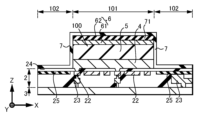
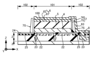
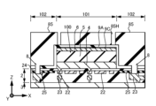
- FIG. 1 is a cross-sectional view illustrating a schematic overall configuration of a solid-state imaging device according to a first embodiment of the present disclosure
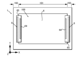
- FIG. 2 is a schematic plan view of the solid-state imaging device shown in FIG. 1
- FIG. 1. It is 1st process sectional drawing explaining the manufacturing method of the solid-state imaging device shown by FIG. It is a 2nd process sectional drawing. It is a 3rd process sectional drawing. It is a 4th process sectional drawing. It is a 5th process sectional drawing. It is 6th process sectional drawing. It is a 7th process sectional drawing. It is 8th process sectional drawing. It is 9th process sectional drawing. It is a 10th process sectional drawing. It is 11th process sectional drawing.
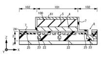
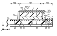
- FIG. 2 is a cross-sectional view corresponding to FIG. 1 and illustrating a schematic overall configuration of a solid-state imaging device according to a second embodiment of the present disclosure
- 16A to 16C are cross-sectional views of the first process for explaining the method of manufacturing the solid-state imaging device shown in FIG. 15; It is a 2nd process sectional drawing. It is a 3rd process sectional drawing. It is a 4th process sectional drawing. It is a 5th process sectional drawing. It is 6th process sectional drawing. It is a 7th process sectional drawing. It is 8th process sectional drawing. It is 9th process sectional drawing.
- FIG. 11 is a cross-sectional view corresponding to FIG.
- FIG. 12 is a cross-sectional view corresponding to FIG. 1 and illustrating a schematic overall configuration of a solid-state imaging device according to a fourth embodiment of the present disclosure;
- FIG. 12 is a cross-sectional view corresponding to FIG. 1 and illustrating a schematic overall configuration of a solid-state imaging device according to a fourth embodiment of the present disclosure;
- FIG. 12 is a cross-sectional view corresponding to FIG. 1 and illustrating a schematic overall configuration of a solid-state imaging device according to a fourth embodiment of the present disclosure;
- FIG. 12 is a cross-sectional view corresponding to FIG. 1 and illustrating a schematic overall configuration of a solid-state imaging device according to a fourth embodiment of the present disclosure;
- FIG. 12 is a cross-sectional view corresponding to FIG. 1 and illustrating a schematic overall configuration of a solid-state imaging device according to a fourth embodiment of the present disclosure;
- FIG. 12 is a cross-sectional view corresponding to FIG. 1 and illustrating a schematic overall
- FIG. 36 is a cross-sectional view of the first step for explaining the manufacturing method of the solid-state imaging device shown in FIG. 35; It is a 2nd process sectional drawing. It is a 3rd process sectional drawing. It is a 4th process sectional drawing. It is a 5th process sectional drawing. It is 6th process sectional drawing.
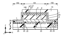
- FIG. 11 is a cross-sectional view corresponding to FIG. 1 and illustrating a schematic overall configuration of a solid-state imaging device according to a fifth embodiment of the present disclosure;
- FIG. 43 is a cross-sectional view of the first step for explaining the manufacturing method of the solid-state imaging device shown in FIG. 42; It is a 2nd process sectional drawing. It is a 3rd process sectional drawing.
- FIG. 21 is a cross-sectional view corresponding to FIG. 1 and illustrating a schematic overall configuration of a solid-state imaging device according to a seventh embodiment of the present disclosure
- 51 is a cross-sectional view of the first step for explaining the manufacturing method of the solid-state imaging device shown in FIG. 50
- FIG. It is a 2nd process sectional drawing. It is a 3rd process sectional drawing. It is a 4th process sectional drawing.
- FIG. 21 is a cross-sectional view corresponding to FIG. 1 and illustrating a schematic overall configuration of a solid-state imaging device according to a ninth embodiment of the present disclosure
- FIG. 58 is a cross-sectional view of the first step for explaining the manufacturing method of the solid-state imaging device shown in FIG. 57; It is a 2nd process sectional drawing. It is a 3rd process sectional drawing. It is a 4th process sectional drawing. It is a 5th process sectional drawing.
- FIG. 21 is a cross-sectional view corresponding to FIG. 1 and illustrating a schematic overall configuration of a solid-state imaging device according to a ninth embodiment of the present disclosure
- FIG. 58 is a cross-sectional view of the first step for explaining the manufacturing method of the solid-state imaging device shown in FIG. 57; It is a 2nd process sectional drawing. It is a 3rd process sectional drawing. It is a 4th process sectional drawing. It is a 5th process sectional drawing.
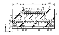
- FIG. 20 is a cross-sectional view illustrating a schematic overall configuration of a solid-state imaging device according to a tenth embodiment of the present disclosure
- FIG. 64 is a schematic plan view of the solid-state imaging device shown in FIG. 63
- FIG. 63 is a cross-sectional view of the first step for explaining the manufacturing method of the solid-state imaging device shown in FIG. 62; It is a 2nd process sectional drawing. It is a 3rd process sectional drawing. It is a 4th process sectional drawing. It is a 5th process sectional drawing. It is 6th process sectional drawing. It is a 7th process sectional drawing. It is 8th process sectional drawing. It is 9th process sectional drawing.
- FIG. 64 is a schematic plan view of the solid-state imaging device shown in FIG. 63
- FIG. 63 is a cross-sectional view of the first step for explaining the manufacturing method of the solid-state imaging device shown in FIG. 62; It is a 2nd process sectional drawing.
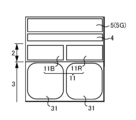
- FIG. 20 is a cross-sectional view illustrating the configuration of a modeled pixel unit of a solid-state imaging device according to an eleventh embodiment of the present disclosure
- FIG. 74 is a cross-sectional view corresponding to FIG. 74 of the solid-state imaging device according to the twelfth embodiment of the present disclosure
- FIG. 74 is a cross-sectional view corresponding to FIG. 74 of the solid-state imaging device according to the thirteenth embodiment of the present disclosure
- 74 is a cross-sectional view corresponding to FIG. 74 of the solid-state imaging device according to the fourteenth embodiment of the present disclosure
- FIG. 74 is a cross-sectional view corresponding to FIG. 74 of the solid-state imaging device according to the fifteenth embodiment of the present disclosure
- FIG. 74 is a cross-sectional view corresponding to FIG. 74 of the solid-state imaging device according to the fifteenth embodiment of the present disclosure
- FIG. 74 is a cross-sectional view corresponding to FIG. 74 of
- First Embodiment A first embodiment describes an example in which the present technology is applied to a solid-state imaging device. 1st Embodiment demonstrates in detail about the cross-sectional structure of a solid-state imaging device, a planar structure, and a manufacturing method. 2. Second Embodiment A second embodiment will explain an example in which the structure of the side surface of the pixel portion and the peripheral region are changed in the solid-state imaging device according to the first embodiment. In the second embodiment, the cross-sectional configuration and manufacturing method of the solid-state imaging device will also be described in detail. 3.
- Third Embodiment A third embodiment describes an example in which the structure of the side surface of the pixel portion is changed in the solid-state imaging device according to the first embodiment. In the third embodiment, the cross-sectional configuration and manufacturing method of the solid-state imaging device will also be described in detail. 4. Fourth Embodiment A fourth embodiment describes an example in which the structure of the side surface of the pixel portion is changed in the solid-state imaging device according to the third embodiment. In the fourth embodiment, the cross-sectional configuration and manufacturing method of the solid-state imaging device will also be described in detail. 5. Fifth Embodiment A fifth embodiment will explain an example in which the structure of the side surface of the pixel portion, particularly the structure of the sidewall insulator, is changed in the solid-state imaging device according to the first embodiment.
- the cross-sectional configuration and manufacturing method of the solid-state imaging device will also be described in detail. 6.
- Sixth Embodiment A sixth embodiment will explain an example in which the manufacturing method of the side wall insulator of the solid-state imaging device according to the fifth embodiment is changed in the solid-state imaging device according to the fifth embodiment. 7.
- Seventh Embodiment In the seventh embodiment in the solid-state imaging device according to the fifth embodiment, an example in which the structure of the transparent electrode of the pixel portion and the wiring for connecting the transparent electrode and the connection portion of the peripheral region is changed. explain.
- the cross-sectional configuration and manufacturing method of the solid-state imaging device will also be described in detail. 8.
- Thirteenth Embodiment A thirteenth embodiment is a third example for explaining the structure of a solid-state imaging device to which the present technology is applicable. 14.
- Fourteenth Embodiment A fourteenth embodiment is a fourth example for explaining the structure of a solid-state imaging device to which the present technology is applicable.
- Fifteenth Embodiment A fifteenth embodiment is a fifth example for explaining the structure of a solid-state imaging device to which the present technology is applicable. 16.
- the arrow X direction shown as appropriate indicates one plane direction of the solid-state imaging device 1 placed on a plane for convenience.
- the arrow Y direction indicates another planar direction perpendicular to the arrow X direction.
- the arrow Z direction indicates an upward direction orthogonal to the arrow X direction and the arrow Y direction. That is, the arrow X direction, the arrow Y direction, and the arrow Z direction exactly match the X-axis direction, the Y-axis direction, and the Z-axis direction of the three-dimensional coordinate system, respectively. It should be noted that each of these directions is illustrated to aid understanding of the description, and does not limit the direction of the present technology.
- FIG. 1 shows an example of a vertical cross-sectional configuration of the solid-state imaging device 1 .
- FIG. 2 shows an example of a planar configuration of the solid-state imaging device 1. As shown in FIG.
- the solid-state imaging device 1 is located at the center of the insulator 2 when viewed in the direction of arrow Y (hereinafter simply referred to as "in side view") and in the direction of arrow Z (hereinafter simply referred to as "in plan view”). It has an effective pixel region 101 having a pixel portion 100 in its portion. Furthermore, the solid-state imaging device 1 includes a peripheral region 102 around the effective pixel region 101 on the insulator 2 . Although the shape is not particularly limited, the effective pixel region 101 is formed in a rectangular shape in which the length in the direction of the arrow Y is shorter than the length in the direction of the arrow X in plan view. The overall planar shape of the solid-state imaging device 1 is formed into a rectangular shape that is one size larger than the effective pixel region 101 by adding a peripheral region 102 around the effective pixel region 101 .
- the insulator 2 is laminated on the base 3 . Although a detailed description of the structure is omitted, the insulator 2 covers the multi-layer wiring, connection hole wiring, etc., and has insulation and environmental resistance.
- a visible light transmission filter (not shown) is disposed inside the insulator 2, and the insulator 2 covers and protects this visible light transmission filter.
- the visible light transmission filter for example, an infrared transmission filter (IRPF) is used (see reference numeral 26 shown in FIG. 74). Silicon oxide (for example, SiO) is used for the insulator 2, for example.
- wiring 22 is arranged inside the insulator 2 in the light transmission region. A transparent electrode material is used for the wiring 22 .
- ITO indium tin oxide
- a wiring 23 is arranged between the wiring 22 and the base 3 to electrically connect the two.
- Metal wiring such as tungsten (W) is used for the wiring 23 .
- an insulating film 24 is formed on the uppermost layer of the insulator 2 .
- the insulating film 24 is made of SiOx, for example.
- an insulating film 25 is formed under the insulating film 24 in the peripheral region 102 .
- the insulating film 25 is made of silicon nitride (SiN), for example.
- the substrate 3 is formed by alternately laminating a plurality of semiconductor layers and insulating layers in which multilayer wiring is arranged.
- a photodiode is formed in the semiconductor layer stacked closest to the insulator 2 (see, for example, reference numeral 31 shown in FIG. 74).
- a plurality of photodiodes are arranged at regular intervals in the arrow X direction and the arrow Y direction.
- the photodiode is configured as a photodetector.
- a photodetector circuit, a control circuit, and the like are arranged in the semiconductor layer separated from the insulator 2 with the semiconductor layer including the photodiode interposed therebetween.
- the photodetection circuit reads out a photodetection signal from the photodiode.
- the control circuit controls the operation of the pixel section 100, the photodetector circuit, and the like.
- the pixel section 100 arranged in the effective pixel area 101 includes a transparent semiconductor 4, an organic photoelectric conversion film 5, and a transparent electrode 6 as main components.
- a transparent semiconductor 4 is laminated on the insulator 2 . Electrons converted from light in the organic photoelectric conversion film 5 are accumulated in the transparent semiconductor 4 . Further, the transparent semiconductor 4 is connected to the photodetector arranged on the substrate 3 through a multilayer wiring (not shown) formed inside the insulator 2, and the accumulated electrons are transferred to the photodetector. be done.
- the transparent semiconductor 4 is an oxide semiconductor that transmits electromagnetic waves in the visible light range.
- IGZO containing indium (In), gallium (Ga), zinc (Zn), and oxygen (O) is used.
- the transparent semiconductor 4 is formed with a thickness of 1 nm or more and 10000 nm or less, for example.
- the organic photoelectric conversion film 5 is laminated on the transparent semiconductor 4 . In the organic photoelectric conversion film 5, electrons are generated from light incident from the arrow Z direction.
- the organic photoelectric conversion film 5 uses an organic material as a light receiving element material. As the organic material, any organic film capable of photoelectric conversion may be used.
- the organic photoelectric conversion film 5 is formed with a thickness of 1 nm or more and 100 ⁇ m or less, for example.
- a transparent electrode 6 is laminated on the organic photoelectric conversion film 5 .
- the transparent electrode 6 is configured as a common electrode over the entire area of the pixel section 100 , and electricity applied to the entire area of the organic photoelectric conversion film 5 is supplied to the transparent electrode 6 .
- the transparent electrode 6 includes a first transparent electrode 61 and a second transparent electrode 62 laminated on the opposite side of the first transparent electrode 61 to the organic photoelectric conversion film 5 in the first embodiment.
- the first transparent electrode 61 is made of indium oxide-zinc oxide (IZO) here.
- the first transparent electrode 61 is formed with a thickness of, for example, 1 nm or more and 1000 nm or less. The thickness of the first transparent electrode 61 is formed thinner than the thickness of the second transparent electrode 62 .
- the second transparent electrode 62 is made of the same transparent electrode material as the first transparent electrode 61 here.
- the second transparent electrode 62 is formed with a thickness of, for example, 1 nm or more and 1000 nm or less.
- the thickness of the second transparent electrode 62 is formed thicker than the thickness of the first transparent electrode 61 . This increases the thickness of the transparent electrode 6 having the first transparent electrode 61 and the second transparent electrode 62, so that the resistance value of the transparent electrode 6 can be reduced.
- the second transparent electrode 62 is used for the wiring 63, the resistance value of the wiring 63 can also be reduced.
- the transparent electrode 6 may be formed of a transparent electrode material other than IZO.
- the transparent electrode 6 may be formed using one or more transparent electrode materials selected from ITO, tin oxide (SnOx), zinc oxide (ZnOx), titanium oxide (TiOx) and silver (Ag) nanowires.
- the transparent electrode 6 may be made of a different transparent electrode material for the second transparent electrode 62 than the transparent electrode material for the first transparent electrode 61 . This specific example will be described in detail in the solid-state imaging device 1 according to the seventh embodiment, which will be described later.
- a protective film 9 covering the transparent electrode 6 is formed on the transparent electrode 6 in the effective pixel region 101 .
- the protective film 9 is made of, for example, aluminum oxide (AlO), which has insulating properties and environmental resistance.
- AlO aluminum oxide
- the protective film 9 is formed with a thickness of, for example, 1 nm or more and 1000 nm or less.
- a color filter and an optical lens are sequentially laminated on the protective film 9 .
- the color filter is made of, for example, a resin material to which dyes of red, blue, and green, which are the three primary colors of light, are added.
- the optical lens is made of, for example, a resin material curved in the arrow Z direction.
- the connecting portion 8 is arranged on the insulator 2 .
- the connection portion 8 is arranged on the right side of the effective pixel area 101 in the side view shown in FIG. 1 and the plan view shown in FIG.
- the connection portion 8 may be arranged on the left side of the effective pixel area 101, or may be arranged above or below the effective pixel area 101 in plan view.
- the connection portion 8 is not limited to one location, and may be arranged at a plurality of locations on the right and left sides of the effective pixel area 101, for example.
- the connecting portions 8 are provided at a plurality of locations is described (see FIG. 64).
- the connection portion 8 is connected to the transparent electrode 6 of the pixel portion 100 through the wiring 63 . That is, the connecting portion 8 is connected to a circuit (not shown) arranged on the substrate 3 and supplies electricity from this circuit to the transparent electrode 6 through the wiring 63 .
- the circuit may be the aforementioned control circuit or a power supply circuit.
- the wiring 63 is made of the same transparent electrode material as the second transparent electrode 62 of the transparent electrode 6 in the first embodiment. Furthermore, it is formed of the same conductive layer as the second transparent electrode 62 . That is, the second transparent electrode 62 constructs the transparent electrode 6 of the pixel section 100 in the effective pixel area 101 and extends from the effective pixel area 101 to the peripheral area 102 to form the wiring 63 .
- the wiring 63 is connected to the multi-layered wiring 23 formed inside the insulator 2 to form the connecting portion 8 . Since the wiring 63 is formed using the second transparent electrode 62 which is a part of the transparent electrodes 6, the thickness of the wiring 63 is formed thinner than the thickness of the transparent electrode 6. As shown in FIG.
- the wiring 63 extends in the vertical direction (opposite to the arrow Z direction) along the side surface of the pixel section 100 from the connection point with the transparent electrode 6 on the right side of the effective pixel area 101 .
- the wiring 63 extends in the horizontal direction (the arrow X direction) in the peripheral region 102 .
- the wiring 63 connects between the transparent electrode 6 and the connecting portion 8 at the shortest distance without running on the protective film 9, for example.
- sidewall insulators 7 are formed between the side surfaces of the pixel section 100 and the wiring 63, as shown in FIG.
- the side wall insulator 7 is made of, for example, AlO, which has insulating properties and environmental resistance.
- the sidewall insulator 7 is formed with a thickness of, for example, 1 nm or more and 1000 nm or less from the side surface of the pixel section 100 toward the peripheral region 102 .
- a protective film 9 is formed on the wiring 63 in the peripheral region 102 to cover the wiring 63 .
- the protective film 9 is made of the same material as the protective film 9 on the effective pixel region 101 and is formed in the same layer.
- a light shielding film 10 is formed on the protective film 9 in the peripheral region 102 .
- the light shielding film 10 is made of a material that does not transmit light.
- the light shielding film 10 is formed of a metal material such as tungsten (W), or a resin material colored black (for example, black resist).
- W tungsten
- the light shielding film 10 is formed with a thickness of, for example, 1 nm or more and 1000 ⁇ m or less.
- the light shielding film 10 is formed with a thickness of, for example, 1 nm or more and 1000 ⁇ m or less.
- the transparent semiconductor 4 the organic photoelectric conversion film 5, the first transparent electrode 61 of the transparent electrode 6, and the mask 71 are sequentially formed on the insulator 2. .
- the first transparent electrode 61 , the organic photoelectric conversion film 5 , and the transparent semiconductor 4 are each patterned using the uppermost mask 71 .
- Amorphous carbon for example, is used as the mask 71 .
- the sidewall insulator 7 is formed over the entire surface including the mask 71 in the effective pixel region 101 and the insulator 2 in the peripheral region 102 .
- the sidewall insulator 7 is also formed on the side surfaces of the pixel section 100 in the effective pixel area 101, the peripheral area 102 and the boundary area. That is, the sidewall insulator 7 is formed along the side surface of the transparent semiconductor 4 , the side surface of the organic photoelectric conversion film 5 and the side surface of the first transparent electrode 61 .
- the sidewall insulator 7 is made of AlO, for example.
- the sidewall insulator 7 is formed, for example, by an atomic layer deposition (ALD) method.
- ALD atomic layer deposition
- the sidewall insulator 7 on the mask 71 in the effective pixel region 101 and the sidewall insulator 7 on the insulator 2 in the peripheral region 102 are removed, and the sidewall insulator 7 is formed on the side surface of the pixel portion 100. As shown in FIG. It is formed.
- An anisotropic etching method such as a reactive ion etching (RIE: Reactive Ion Etching) method is used to remove the sidewall insulator 7 .
- RIE reactive ion etching
- a mask 72 is formed over the effective pixel area 101 and the peripheral area 102 .
- the mask 72 is formed on the mask 71 in the effective pixel area 101 and on the insulator 2 in the peripheral area 102 .
- An opening 72H is formed in the mask 72 at the connection portion 8 (see FIGS. 1 and 2) in the peripheral region 102 .
- the mask 72 is made of photoresist, for example.
- the insulator 2 exposed through the openings 72H of the mask 72 is removed, and the surface of the wiring 23 inside the insulator 2 is exposed.
- An RIE method for example, is used to remove the insulator 2 . After this, as shown in FIG. 8, the mask 72 is removed.
- the mask 71 on the first transparent electrode 61 is removed.
- the surface of the first transparent electrode 61 is exposed.
- the second transparent electrode 62 is formed over the entire surface including the first transparent electrode 61 in the effective pixel area 101 and the insulator 2 in the peripheral area 102 . Since the second transparent electrode 62 is laminated on the first transparent electrode 61 in the effective pixel region 101, the transparent electrode 6 composed of the first transparent electrode 61 and the second transparent electrode 62 is formed.
- a mask 73 is formed to cover the transparent electrode 6 in the effective pixel area 101 and the portion from the transparent electrode 6 to the connecting portion 8 .
- the mask 73 is made of photoresist, for example.
- a mask 73 is used to remove excess second transparent electrode 62 in peripheral region 102 . Subsequently, mask 73 is removed, as shown in FIG. As a result, the wiring 63 is formed integrally with the second transparent electrode 62 of the transparent electrode 6, is formed of the same transparent electrode material as the second transparent electrode 62, and is made of the same conductive layer as the second transparent electrode 62. It is formed. This wiring 63 is connected to the wiring 23 at the connecting portion 8 . In addition, the wiring 63 is electrically separated from the side surface of the transparent semiconductor 4 of the pixel section 100, the side surface of the organic photoelectric conversion film 5, and the side surface of the first transparent electrode 61 of the transparent electrode 6 with the side wall insulator 7 interposed. be done.
- the protective film 9 is formed over the entire surface including the transparent electrodes 6 in the effective pixel region 101, the wirings 63 in the peripheral region 102, and the connecting portions 8 in the peripheral region 102. As shown in FIG. Subsequently, as shown in FIG. 1 described above, the light shielding film 10 is formed on the protective film 9 in the peripheral region 102 . When a series of these manufacturing steps are completed, the solid-state imaging device 1 according to the first embodiment is completed.
- the solid-state imaging device 1 includes a pixel portion 100 having a transparent semiconductor 4, an organic photoelectric conversion film 5, and a transparent electrode 6; and wiring 63 .
- a transparent semiconductor 4 is formed in an effective pixel region 101 of the insulator 2 .
- the organic photoelectric conversion film 5 is formed on the side of the transparent semiconductor 4 opposite to the insulator 2 .
- the transparent electrode 6 is formed on the side of the organic photoelectric conversion film 5 opposite to the transparent semiconductor 4 .
- the connection portion 8 is arranged in the insulator 2 in the peripheral region 102 around the effective pixel region 101 and connected to a circuit that supplies electricity to the transparent electrode 6 .
- the wiring 63 electrically connects between the transparent electrode 6 and the connecting portion 8 and is formed of a transparent electrode material. Therefore, the wiring 63 is formed by extending at least a part of the transparent electrode 6 , and the transparent electrode 6 and the connecting portion 8 can be directly connected by the wiring 63 . In other words, there is no need to form connection holes on the transparent electrode 6 of the protective film 9 and on the connection portion 8 of the protective film 9 , and there is no need to route wires over these connection holes and the protective film 9 . Thereby, the wiring structure for connecting the transparent electrode 6 and the connection portion 8 can be simplified. Moreover, since the wiring 63 is not routed, the wiring length of the wiring 63 is shortened, and the wiring resistance of the wiring 63 can be reduced.
- the wiring 63 is formed to have a thickness smaller than the thickness of the transparent electrode 6, as shown in FIG. In other words, the thickness of the transparent electrode 6 is formed thicker than the thickness of the wiring 63 . Therefore, the resistance value of the transparent electrode 6 of the pixel section 100 can be reduced in the effective pixel region 101, so that uniform photoelectric conversion can be realized in the entire pixel section 100.
- FIG. since the wiring 63 is formed thin, the second transparent electrode 62 can be easily processed in the manufacturing method of the solid-state imaging device 1, as shown in FIGS.
- the transparent electrode 6 includes a first transparent electrode 61 and a second transparent electrode 62, as shown in FIG.
- a first transparent electrode 61 is formed on the organic photoelectric conversion film 5 .
- the second transparent electrode 62 is formed on the opposite side of the first transparent electrode 61 to the organic photoelectric conversion film 5 . Therefore, since the transparent electrode 6 is formed thickly by overlapping the first transparent electrode 61 and the second transparent electrode 62, the resistance value of the transparent electrode 6 can be reduced.
- the wiring 63 is formed on the same conductive layer as at least part of the transparent electrode 6 . Specifically, the wiring 63 is formed on the same conductive layer as the second transparent electrode 62 of the transparent electrode 6 . Therefore, as described above, the wiring structure can be simplified and the wiring resistance of the wiring 63 can be reduced.
- the solid-state imaging device 1 also includes sidewall insulators 7, as shown in FIG.
- the sidewall insulator 7 is formed on the side surface of the organic photoelectric conversion film 5 and the side surface of the transparent semiconductor 4 .
- the wiring 63 extends from the transparent electrode 6 to the connection portion 8 along the side surface of the organic photoelectric conversion film 5 and the side surface of the transparent semiconductor 4 with the side wall insulator 7 interposed therebetween. Therefore, the wiring 63 is reliably electrically isolated from the pixel section 100 , specifically from the organic photoelectric conversion film 5 and the transparent semiconductor 4 , by the sidewall insulator 7 .
- the sidewall insulator 7 can improve the environmental resistance of the pixel section 100 .
- a protective film 9 is formed in the effective pixel region 101 and the peripheral region 102 to cover the transparent electrodes 6 and the wirings 63.
- the environmental resistance can be improved in the pixel portion 100 of the effective pixel region 101 and the connection portion 8 of the peripheral region 102 .
- the light shielding film 10 is formed on the opposite side of the protective film 9 from the wiring 63 to block light. Thereby, the incidence of light in the peripheral area 102 can be blocked.
- Second Embodiment> A solid-state imaging device 1 according to a second embodiment of the present disclosure will be described with reference to FIGS. 15 to 24.
- FIG. 15 shows an example of a vertical cross-sectional configuration of the solid-state imaging device 1.
- the side wall insulator 7 formed on the side surface of the pixel section 100 acts as a barrier between the insulator 2 in the peripheral region 102 and the protective film 9. is also formed between
- the sidewall insulators 7 formed on the side surfaces of the pixel section 100 and the peripheral region 102 are made of the same insulating material and formed on the same insulating layer. That is, the sidewall insulator 7 formed on the side surface of the pixel section 100 extends to the peripheral region 102 .
- Components other than the components described above are the same or substantially the same as the components of the solid-state imaging device 1 according to the first embodiment described above.
- Side wall insulators 7 are formed in the same manner as in the process shown in FIG. 4 of the method for manufacturing the solid-state imaging device 1 according to the first embodiment (hereinafter simply referred to as "first manufacturing method").
- the sidewall insulator 7 is formed on the entire surface including the mask 71 in the effective pixel region 101 and the insulator 2 in the peripheral region 102 .
- a mask 72 is formed on the entire surface of the effective pixel region 101 and the peripheral region 102, as shown in FIG.
- a mask 72 is formed on the sidewall insulator 7 in each of the effective pixel area 101 and the peripheral area 102 .
- An opening 72H is formed in the mask 72 at the formation location of the connecting portion 8 (see FIG. 15) in the peripheral region 102 .
- the side wall insulator 7 and the insulator 2 exposed through the opening 72H of the mask 72 are removed, and the inner portion of the insulator 2 is removed as shown in FIG.
- the surface of the wiring 23 is exposed.
- the RIE method is used to remove the sidewall insulator 7 and the insulator 2 .
- mask 72 is removed as shown in FIG. 18, similarly to the step shown in FIG. 8 of the first manufacturing method.
- the mask 71 is selectively removed in the effective pixel area 101 using a lift-off method. As the mask 71 is removed, the side wall insulator 7 on the mask 71 is removed in the effective pixel region 101 .
- a second transparent electrode 62 is formed on the entire surface including the body 7 . Since the second transparent electrode 62 is laminated on the first transparent electrode 61 in the effective pixel region 101, the transparent electrode 6 composed of the first transparent electrode 61 and the second transparent electrode 62 is formed.
- a mask 73 is used to remove excess second transparent electrode 62 in peripheral region 102, as shown in FIG. Subsequently, mask 73 is removed, as shown in FIG. As a result, the wiring 63 is formed integrally with the second transparent electrode 62 of the transparent electrode 6, is formed of the same transparent electrode material as the second transparent electrode 62, and is made of the same conductive layer as the second transparent electrode 62. It is formed. This wiring 63 is connected to the wiring 23 at the connecting portion 8 .
- the wiring 63 is electrically separated from the side surface of the transparent semiconductor 4 of the pixel section 100, the side surface of the organic photoelectric conversion film 5, and the side surface of the first transparent electrode 61 of the transparent electrode 6 with the side wall insulator 7 interposed. be done.
- the solid-state imaging device 1 according to the second embodiment is completed.
- the solid-state imaging device 1 includes sidewall insulators 7 on the sides of the organic photoelectric conversion film 5 and the sides of the transparent semiconductor 4, as shown in FIG.
- the wiring 63 extends from the transparent electrode 6 to the connecting portion 8 along the side surface of the organic photoelectric conversion film 5 and the side surface of the transparent semiconductor 4 with the side wall insulator 7 interposed.
- sidewall insulator 7 extends between insulator 2 and protective film 9 in peripheral region 102 . That is, the sidewall insulator 7 formed on the side surface of the organic photoelectric conversion film 5 and the side surface of the transparent semiconductor 4 is used in the peripheral region 102, and the sidewall insulator 7 reduces the effective thickness of the insulator 2 or the protective film 9. can be thickened. Therefore, in the peripheral region 102, environmental resistance can be further improved.
- FIG. 25 shows an example of a vertical cross-sectional configuration of the solid-state imaging device 1.
- the side wall formed on the side surface of the pixel section 100 in the solid-state imaging device 1 according to the first embodiment or the second embodiment The insulator 7 is not formed (see FIGS. 1 and 15).
- a natural oxide film (not shown) is effectively formed on the side surface of the pixel section 100 and at least on the side surface of the transparent semiconductor 4 . That is, the wiring 63 and the transparent semiconductor 4 are electrically separated by the natural oxide film.
- Components other than the components described above are the same or substantially the same as the components of the solid-state imaging device 1 according to the first embodiment or the second embodiment.
- the transparent semiconductor 4, the organic photoelectric conversion film 5, the first transparent electrode 61 of the transparent electrode 6, and the mask 71 are formed on the insulator 2 in the same manner as in the steps shown in FIGS. are formed in sequence.
- the first transparent electrode 61 , the organic photoelectric conversion film 5 , and the transparent semiconductor 4 are each patterned using the uppermost mask 71 .
- a mask 72 is formed on the entire surface of the effective pixel region 101 and the peripheral region 102 in the same manner as in the steps shown in FIG. 6 of the first manufacturing method.
- the mask 72 is formed on the mask 71 in the effective pixel area 101 and on the insulator 2 in the peripheral area 102 .
- An opening 72H is formed in the mask 72 at the formation location of the connecting portion 8 (see FIG. 25) in the peripheral region 102 .
- the insulator 2 exposed through the openings 72H of the mask 72 is removed as shown in FIG. exposed. Thereby, the connecting portion 8 is substantially formed. After this, as shown in FIG. 28, the mask 72 is removed.
- the mask 71 on the first transparent electrode 61 is removed in the effective pixel region 101 as shown in FIG.
- the mask 71 is removed, the surface of the first transparent electrode 61 is exposed.
- the second transparent electrode 61 is formed on the entire surface including the first transparent electrode 61 in the effective pixel region 101 and the insulator 2 in the peripheral region 102. As shown in FIG. Electrodes 62 are formed. Since the second transparent electrode 62 is laminated on the first transparent electrode 61 in the effective pixel region 101, the transparent electrode 6 composed of the first transparent electrode 61 and the second transparent electrode 62 is formed.
- the wiring 63 is formed integrally with the second transparent electrode 62 of the transparent electrode 6, is formed of the same transparent electrode material as the second transparent electrode 62, and is made of the same conductive layer as the second transparent electrode 62. It is formed. This wiring 63 is connected to the wiring 23 at the connecting portion 8 . Moreover, the wiring 63 is electrically isolated from the side surface of the transparent semiconductor 4 of the pixel section 100 with a natural oxide film (not shown) interposed therebetween.
- FIG. 25 Similar to the steps shown in FIG. 14 of the first manufacturing method, as shown in FIG. A protective film 9 is formed on the entire surface including. Subsequently, as shown in FIG. 25 described above, the light shielding film 10 is formed on the protective film 9 in the peripheral region 102 . When a series of these manufacturing steps are finished, the solid-state imaging device 1 according to the third embodiment is completed.
- the sidewall insulators 7 are not intentionally formed on the side surfaces of the pixel section 100. As shown in FIG. Therefore, the component corresponding to the side wall insulator 7 can be omitted, and the wiring structure can be further simplified. In addition, since the process corresponding to the process of forming the sidewall insulator 7 can be omitted, the number of manufacturing processes of the solid-state imaging device 1 can be reduced. As a result, the manufacturing yield of the solid-state imaging device 1 can be improved.
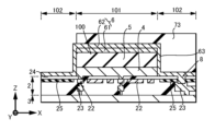
- FIG. 35 shows an example of a vertical cross-sectional configuration of the solid-state imaging device 1.
- FIG. 35 in the solid-state imaging device 1 according to the fourth embodiment, similarly to the solid-state imaging device 1 according to the third embodiment, sidewall insulators 7 are not formed (see FIG. 25). .
- a cavity 4 ⁇ /b>S is formed between the side surface of the transparent semiconductor 4 of the pixel section 100 and the wiring 63 .
- a cavity 4 ⁇ /b>S is formed between the side surface of the transparent semiconductor 4 and the wiring 63 by forming the side surface of the transparent semiconductor 4 inside the effective pixel region 101 with respect to the side surface of the organic photoelectric conversion film 5 .
- the cavity 4S is filled with gas such as air.
- the transparent semiconductor 4 and the wiring 63 are electrically isolated from each other by gas.
- Components other than the components described above are the same or substantially the same as the components of the solid-state imaging device 1 according to the third embodiment.
- third manufacturing method in the manufacturing method of the solid-state imaging device 1 according to the third embodiment (hereinafter simply referred to as "third manufacturing method"), in the effective pixel region 101, on the first transparent electrode 61 mask 71 is removed.
- the mask 71 is removed, the surface of the first transparent electrode 61 is exposed.
- side etching is performed on the side surface of the transparent semiconductor 4 in the effective pixel region 101 .
- an isotropic etching method for example, which has a high etching selectivity of the transparent semiconductor 4 with respect to the organic photoelectric conversion film 5 and the insulator 2, is used.
- the side surface of the transparent semiconductor 4 recedes inside the effective pixel region 101 to form a cavity 4S.
- the second transparent electrode 61 is applied over the entire surface including the first transparent electrode 61 in the effective pixel area 101 and the insulator 2 in the peripheral area 102. As shown in FIG. Electrodes 62 are formed. Since the second transparent electrode 62 is laminated on the first transparent electrode 61 in the effective pixel region 101, the transparent electrode 6 composed of the first transparent electrode 61 and the second transparent electrode 62 is formed.
- a mask 73 is used to remove excess second transparent electrode 62 in peripheral region 102 . Subsequently, mask 73 is removed, as shown in FIG. As a result, the wiring 63 is formed integrally with the second transparent electrode 62 of the transparent electrode 6, is formed of the same transparent electrode material as the second transparent electrode 62, and is made of the same conductive layer as the second transparent electrode 62. It is formed. This wiring 63 is connected to the wiring 23 at the connecting portion 8 .
- the wiring 63 is arranged on the side surface of the transparent semiconductor 4 with the cavity 4S (the gas filled in the cavity 4S) interposed therebetween. electrically isolated.
- FIG. 34 of the third manufacturing method Similar to the process shown in FIG. 34 of the third manufacturing method, as shown in FIG. 35 described above, the light shielding film 10 is formed on the protective film 9 in the peripheral region 102 .
- the solid-state imaging device 1 according to the fourth embodiment is completed.
- the solid-state imaging device 1 includes a cavity 4S between the side surface of the transparent semiconductor 4 of the pixel section 100 and the wiring 63.
- the cavity 4 ⁇ /b>S is formed by arranging the side surface of the transparent semiconductor 4 inside the effective pixel region 101 with respect to the side surface of the organic photoelectric conversion film 5 . That is, the cavity 4S is formed by side etching. Therefore, the wiring 63 is reliably electrically isolated from the pixel section 100, specifically from the transparent semiconductor 4 by the cavity 4S (or the gas filled in the cavity 4S).
- a solid-state imaging device 1 according to a fifth embodiment of the present disclosure will be described with reference to FIGS. 42 to 47.
- FIG. in the solid-state imaging devices 1 according to the fifth to ninth embodiments examples in which the structure of the side wall insulator 7 is changed will be described.
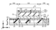
- FIG. 42 shows an example of a vertical cross-sectional configuration of the solid-state imaging device 1.
- the solid-state imaging device 1 according to the fifth embodiment includes sidewall insulators 7, like the solid-state imaging device 1 according to the first embodiment.
- the sidewall insulator 7 is formed on the side surface of the pixel section 100 , that is, at least on the side surface of the organic photoelectric conversion film 5 and the side surface of the transparent semiconductor 4 .
- the side wall insulator 7 includes a first side wall insulator 75 which is the same or substantially the same component as the side wall insulator 7 of the solid-state imaging device 1 according to the first embodiment; and a second sidewall insulator 76 stacked on the first sidewall insulator 75 .
- the second sidewall insulator 76 of the sidewall insulator 7 has an inclined wall surface 7S extending from the effective pixel region 101 to the peripheral region 102 from the transparent electrode 6 toward the transparent semiconductor 4 on the side surface of the pixel section 100 . Since the inclined wall surface 7S is formed, the thickness of the sidewall insulator 7 formed on the side surface of the organic photoelectric conversion film 5 from the side surface of the organic photoelectric conversion film 5 is formed on the side surface of the transparent electrode 6. The thickness of the side wall insulator 7 from the side surface of the transparent electrode 6 is thicker than that of the side wall insulator 7 .
- the thickness of the side wall insulator 7 formed on the side surface of the transparent semiconductor 4 from the side surface of the transparent semiconductor 4 is equal to the thickness of the side wall insulator 7 formed on the side surface of the organic photoelectric conversion film 5 . It is formed thicker than the thickness from the side surface of 5.
- the inclined wall surface 7S is formed flat here.
- an inclination angle ⁇ formed by the inclined wall surface 7S and the surface of the insulator 2 on the effective pixel region 101 side is set to, for example, 20 degrees or more and less than 90 degrees.
- the inclination angle ⁇ is set to 20 degrees or more and less than 60 degrees.
- Components other than the components described above are the same or substantially the same as the components of the solid-state imaging device 1 according to the first embodiment described above.
- first sidewall insulators 75 are formed on the side surfaces of the pixel section 100 (see FIGS. 5 and 43).
- the first sidewall insulator 75 is here, like the sidewall insulator 7 shown in FIG. 5, for example made of AlO.
- An ALD method is used to form the first sidewall insulator 75 .
- insulator 2 is removed in peripheral region 102 to expose the surface of wiring 23 inside insulator 2 .
- the mask 71 on the first transparent electrode 61 is removed in the effective pixel region 101 in the same manner as in the process shown in FIG. 9 of the first manufacturing method.
- the surface of the first transparent electrode 61 is exposed.
- an insulating film 77 is formed over the entire surface including the first transparent electrode 61 in the effective pixel area 101 and the insulator 2 in the peripheral area 102 . Since the insulating film 77 forms the second sidewall insulator 76 of the sidewall insulator 7, it is made of, for example, AlO, which has insulating properties and environmental resistance.
- the insulating film 77 is formed by sputtering or ALD, for example.
- the insulating film 77 is formed to have a thickness that completely embeds the pixel portion 100, for example, 1 nm or more and 100 ⁇ m or less.
- the surface of the insulating film 77 is undulated. That is, the surface of the insulating film 77 is higher in the effective pixel region 101 and lower than the effective pixel region 101 in the peripheral region 102 . As shown in FIG. 44, the surface of insulating film 77 is planarized. A chemical mechanical polishing (CMP) method or an etchback method is used for planarization.
- CMP chemical mechanical polishing
- a mask 81 is formed on the insulating film 77 in the effective pixel region 101 .
- the mask 81 is shown using dashed lines in FIG.
- a photoresist for example, is used as the mask 81 .
- insulating film 77 in peripheral region 102 is removed.
- a dry etching method for example, is used to remove the insulating film 77 .
- the etching conditions are appropriately adjusted, and the second side wall insulator 76 having the inclined wall surface 7S from the insulating film 77 is formed on the side surface of the pixel section 100.
- the sidewall insulator 7 is completed with the first sidewall insulator 75 previously formed on the side surface of the pixel portion 100 and the second sidewall insulator 76 newly formed on the first sidewall insulator 75 . do.
- a mask 82 is formed which covers the insulator 2 and the sidewall insulator 7 in the peripheral region 102 .
- the mask 82 is shown with dashed lines in FIG.
- a photoresist is used like the mask 81.
- FIG. As shown in FIG. 46, the mask 82 is used to remove the insulating film 77 remaining on the first transparent electrode 61 in the effective pixel region 101 .
- a dry etching method for example, is used to remove the insulating film 77 . By removing the insulating film 77, the surface of the first transparent electrode 61 is exposed. Mask 82 is then removed.
- connection portion 8 in the peripheral region 102 is covered with a mask 82 during the removal of the insulating film 77 remaining in the effective pixel region 101 . Therefore, the surface of the wiring 23 exposed at the connecting portion 8 is prevented from being damaged by etching.
- a second transparent electrode 62 is formed on the first transparent electrode 61 in the effective pixel region 101, as shown in FIG.
- the transparent electrode 6 is completed by the first transparent electrode 61 and the second transparent electrode 62 formed on the first transparent electrode 61 .
- a wiring 63 extending from the second transparent electrode 62 to the connecting portion 8 along the inclined wall surface 7S of the side wall insulator 7 is formed in the same step.
- a protective film 9 is formed on the entire surface including the transparent electrodes 6 in the effective pixel region 101, the wirings 63 in the peripheral region 102, and the connecting portions 8 in the peripheral region 102. (See FIG. 42). Subsequently, as shown in FIG. 42 described above, the light shielding film 10 is formed on the protective film 9 in the peripheral region 102 . After a series of these manufacturing steps are completed, the solid-state imaging device 1 according to the fifth embodiment is completed.
- the side wall insulator 7 has an inclined wall surface 7S extending from the effective pixel region 101 toward the transparent semiconductor 4 toward the transparent electrode 6 to the peripheral region. Therefore, the step coverage (adherence) of the wiring 63 extending from the transparent electrode 6 of the pixel section 100 to the connection section 8 along the side wall insulator 7 can be improved. In other words, the reduction in cross-sectional area of the wiring 63 can be effectively suppressed or prevented, so that the resistance value can be reduced. In addition, disconnection of the wiring 63 can be effectively prevented.
- the side wall insulator 7 has the inclined wall surface 7S, the thickness of the side wall insulator 7 formed on the side surface of the organic photoelectric conversion film 5 from the side surface of the organic photoelectric conversion film 5 is equal to that of the transparent electrode 6.
- the sidewall insulator 7 formed on the side surface is formed to be thicker than the thickness from the side surface of the transparent electrode 6 . Therefore, the side surface of the organic photoelectric conversion film 5 can be improved in environmental resistance. This effect is similarly obtained on the side surface of the transparent semiconductor 4 as well.
- the inclination angle ⁇ on the effective pixel area 101 side formed by the inclined wall surface 7S of the side wall insulator 7 and the surface of the insulator 2 is 20 degrees or more and 90 degrees. set to less than If the inclination angle ⁇ is equal to or greater than the above lower limit value, the step coverage of the wiring 63 can be sufficiently improved. Of course, the environmental resistance of the pixel unit 100 can be sufficiently improved.
- FIG. 6th Embodiment demonstrates the modification of the manufacturing method of the solid-state imaging device 1 which concerns on 5th Embodiment.
- an insulating film 77 is formed in the same manner as in the process shown in FIG. 43 of the manufacturing method of the solid-state imaging device 1 according to the fifth embodiment (hereinafter simply referred to as "fifth manufacturing method").
- the insulating film 77 is formed on the entire surface including the first transparent electrode 61 in the effective pixel area 101 and the insulator 2 in the peripheral area 102 .
- the insulating film 77 is also formed on the first sidewall insulator 75 on the side surface of the pixel section 100 .
- the insulating film 77 formed on the first transparent electrode 61 in the effective pixel area 101 and the insulator 2 in the peripheral area 102 is removed.
- the removal of the insulating film 77 exposes the surface of the first transparent electrode 61 in the effective pixel region 101 .
- the insulating film 77 formed on the insulator 2 in the peripheral region 102 is formed thick on the side surface of the pixel portion 100 due to the stepped shape of the pixel portion 100 . part remains.
- a portion of this insulating film 77 is formed as a second sidewall insulator 76 .
- the second side wall insulator 76 is formed with an inclined wall surface 7S.
- the second transparent electrode 62 is formed on the first transparent electrode 61 in the effective pixel region 101, as shown in FIG. After the second transparent electrode 62 is formed, the transparent electrode 6 is completed by the first transparent electrode 61 and the second transparent electrode 62 formed on the first transparent electrode 61 . Further, when the second transparent electrode 62 is formed, a wiring 63 extending from the second transparent electrode 62 to the connecting portion 8 along the inclined wall surface 7S of the side wall insulator 7 is formed in the same step.
- a protective film 9 is formed on the entire surface including the transparent electrodes 6 in the effective pixel region 101, the wirings 63 in the peripheral region 102, and the connecting portions 8 in the peripheral region 102. (See FIG. 42). Subsequently, as shown in FIG. 42 described above, the light shielding film 10 is formed on the protective film 9 in the peripheral region 102 . After a series of these manufacturing steps are completed, the solid-state imaging device 1 according to the sixth embodiment is completed.
- the solid-state imaging device 1 according to the sixth embodiment can obtain the same effects or substantially the same effects as those obtained by the solid-state imaging device 1 according to the fifth embodiment.
- the manufacturing method of the solid-state imaging device 1 after forming the insulating film 77 shown in FIG. 43 of the fifth manufacturing method, as shown in FIG. The surface of the first transparent electrode 61 is exposed and the side wall insulator 7 is formed. That is, in the fifth manufacturing method, the step of planarizing the insulating film 77 shown in FIG. 44, the step of forming the mask 81 and the second sidewall insulator 76 shown in FIG. The step of removing the remaining insulating film 77 is one step. Therefore, in the manufacturing method of the solid-state imaging device 1, the number of manufacturing steps can be significantly reduced. In addition, the manufacturing yield of the solid-state imaging device 1 can be improved by reducing the number of manufacturing steps.
- FIG. 50 to 54 A solid-state imaging device 1 according to a seventh embodiment of the present disclosure will be described with reference to FIGS. 50 to 54.
- FIG. 50 to 54 A solid-state imaging device 1 according to a seventh embodiment of the present disclosure will be described with reference to FIGS. 50 to 54.
- FIG. 50 to 54 A solid-state imaging device 1 according to a seventh embodiment of the present disclosure will be described with reference to FIGS. 50 to 54.
- FIG. 50 shows an example of a vertical cross-sectional configuration of the solid-state imaging device 1.
- the solid-state imaging device 1 according to the seventh embodiment includes transparent electrodes 6, like the solid-state imaging device 1 according to the fifth or sixth embodiment.
- the transparent electrode 6 is formed on the first transparent electrode 61 and the first transparent electrode 61, and the same transparent electrode as the first transparent electrode 61 is formed. and a second transparent electrode 62 formed of an electrode material.
- the transparent electrode 6 includes the first transparent electrode 61 and the second transparent electrode 62 formed of a transparent electrode material different from that of the first transparent electrode 61.
- the first transparent electrode 61 is made of IZO, for example.
- the second transparent electrode 62 is made of ITO, for example.
- the resistance of ITO is smaller than that of IZO. That is, the transparent electrode 6 is formed by laminating the first transparent electrode 61 and the second transparent electrode 62 having different resistance values.
- the wiring 63 that connects the transparent electrode 6 and the connecting portion 8 is made of the same transparent electrode material as the second transparent electrode 62 and is formed on the same conductive layer. That is, here, the wiring 63 is made of ITO, for example.
- Components other than the components described above are the same or substantially the same as the components of the solid-state imaging device 1 according to the fifth embodiment or the sixth embodiment.
- an insulating film 77 is formed over the entire surface including the first transparent electrode 61 in the effective pixel area 101 and the insulator 2 in the peripheral area 102 . Subsequently, as in the step shown in FIG. 44 of the fifth manufacturing method, the surface of insulating film 77 is planarized as shown in FIG. A CMP method or an etchback method is used for planarization.
- a mask 81 is formed on the insulating film 77 in the effective pixel region 101, and the mask 81 is used to insulate the peripheral region 102.
- Film 77 is removed.
- the second side wall insulator 76 having the inclined wall surface 7S is formed from the insulating film 77 on the side surface of the pixel section 100.
- the first sidewall insulator 75 previously formed on the side surface of the pixel portion 100 and the second sidewall insulator 76 newly formed on the first sidewall insulator 75 are formed.
- sidewall insulators 7 are completed.
- the insulating film 77 remaining on the first transparent electrode 61 in the effective pixel area 101 is removed.
- the surface of the first transparent electrode 61 is exposed.
- Mask 82 is then removed.
- the second transparent electrode 62 is formed on the first transparent electrode 61 in the effective pixel region 101 as shown in FIG.
- the second transparent electrode 62 is formed of a transparent electrode material different from that of the first transparent electrode 61 .
- the transparent electrode 6 is completed by the first transparent electrode 61 and the second transparent electrode 62 formed on the first transparent electrode 61 .
- a wiring 63 extending from the second transparent electrode 62 to the connecting portion 8 along the inclined wall surface 7S of the side wall insulator 7 is formed in the same step.
- a protective film 9 is formed on the entire surface including the transparent electrodes 6 in the effective pixel region 101, the wirings 63 in the peripheral region 102, and the connecting portions 8 in the peripheral region 102. (See FIG. 50). Subsequently, as shown in FIG. 50 described above, the light shielding film 10 is formed on the protective film 9 in the peripheral region 102 . After a series of these manufacturing steps are completed, the solid-state imaging device 1 according to the seventh embodiment is completed.
- the transparent electrode 6 is made of a transparent electrode material that makes the resistance of the second transparent electrode 62 smaller than that of the first transparent electrode 61. Therefore, the resistance value of the transparent electrode 6 of the pixel section 100 can be reduced in the effective pixel region 101, so that uniform photoelectric conversion can be realized in the entire pixel section 100.
- the wiring 63 is made of the same transparent electrode material as the second transparent electrode 62, so the wiring resistance of the wiring 63 can be reduced.
- FIG. 8th Embodiment demonstrates the modification of the manufacturing method of the solid-state imaging device 1 which concerns on 6th Embodiment.
- an insulating film is formed in the same manner as in the process shown in FIG. 78 is formed.
- the insulating film 78 is formed on the entire surface including the first transparent electrode 61 in the effective pixel area 101 and the insulator 2 in the peripheral area 102 .
- the insulating film 78 is also formed on the first sidewall insulator 75 on the side surface of the pixel section 100 .
- AlO is used for the insulating film 78, similarly to the insulating film 77 of the solid-state imaging device 1 according to the first to seventh embodiments.
- the insulating film 78 is formed by a mist chemical vapor deposition (MCVD) method or a mist vapor phase epitaxy (MVPE) method.
- MCVD mist chemical vapor deposition
- MVPE mist vapor phase epitaxy
- the insulating film 78 can be formed at a low temperature of 150° C. or less, for example.
- the insulating film 78 formed using such a film formation method is uniform on the first transparent electrode 61 in the effective pixel region 101, the insulator 2 in the peripheral region 102, and the first sidewall insulator 75. thickness.
- the insulating film formed on the first transparent electrode 61 in the effective pixel region 101 and on the insulator 2 in the peripheral region 102 78 is removed.
- a dry etching method for example, is used to remove the insulating film 78 .
- the removal of the insulating film 78 exposes the surface of the first transparent electrode 61 in the effective pixel region 101 .
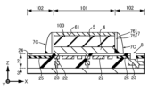
- the insulating film 78 formed on the insulator 2 in the peripheral region 102 is thick at the side surfaces of the pixel portion 100 due to the stepped shape of the pixel portion 100, the insulating film 78 is formed thick. Some remain. Furthermore, since the insulating film 78 is formed using a CVD method and removed using, for example, a dry etching method, a portion of the insulating film 78 is formed as the second sidewall insulator 76 having the curved wall surface 7C.
- the curved wall surface 7C is formed in a curved surface shape extending from the effective pixel region 101 to the peripheral region 102 toward the transparent semiconductor 4 from the first transparent electrode 61 and protruding from the effective pixel region 101 to the peripheral region 102 in a side view. be done.
- Second sidewall insulators 76 are commonly referred to as sidewall spacers.
- the sidewall insulator 7 having the first sidewall insulator 75 and the second sidewall insulator 76 is completed.
- a second transparent electrode 62 is formed on the first transparent electrode 61 in the effective pixel region 101 in the same manner as the step shown in FIG. 47 of the fifth manufacturing method. After the second transparent electrode 62 is formed, the transparent electrode 6 is completed by the first transparent electrode 61 and the second transparent electrode 62 formed on the first transparent electrode 61 . Further, when the second transparent electrode 62 is formed, a wiring 63 is formed along the curved wall surface 7C of the sidewall insulator 7 from the second transparent electrode 62 to the connecting portion 8 in the same step.
- a protective film 9 is formed on the entire surface including the transparent electrodes 6 in the effective pixel region 101, the wirings 63 in the peripheral region 102, and the connecting portions 8 in the peripheral region 102. (See FIG. 42). Subsequently, as shown in FIG. 42 described above, the light shielding film 10 is formed on the protective film 9 in the peripheral region 102 . When a series of these manufacturing steps are finished, the solid-state imaging device 1 according to the eighth embodiment is completed.
- the insulating film 78 is formed with a uniform thickness using the CVD method. Subsequently, as shown in FIG. 56, the insulating film 78 is removed using the RIE method. As a result, side wall insulators 7 having curved wall surfaces 7C are formed on the side surfaces of the pixel section 100 . Therefore, the step coverage of the wiring 63 from the transparent electrode 6 of the pixel section 100 to the connection section 8 along the side wall insulator 7 can be further improved. In other words, the reduction in cross-sectional area of the wiring 63 can be effectively suppressed or prevented, so that the resistance value can be reduced. In addition, disconnection of the wiring 63 can be prevented more effectively.
- FIG. 57 shows an example of a vertical cross-sectional configuration of the solid-state imaging device 1.
- the connecting portion 8 is configured by a laminated structure of the wiring 23 and the wiring 22 laminated on the wiring 23 . That is, the wiring 22 is formed on the wiring 23 instead of the insulating film 25 of the solid-state imaging device 1 according to the fifth embodiment shown in FIG.
- the wiring 23 is made of W, for example.
- the wiring 22 is made of, for example, ITO, which is a transparent electrode material. Therefore, the connection portion 8 has a two-layer structure of the wiring 23 and the wiring 22, and the effective thickness of the wiring layer is increased.
- Components other than the components described above are the same or substantially the same as the components of the solid-state imaging device 1 according to the fifth embodiment.
- Components other than the above components are the same as or substantially the same as the components of the solid-state imaging devices 1 according to the first to fourth embodiments and the sixth to eighth embodiments. is identical to
- the wiring 23 and the wiring 22 laminated on the wiring 23 are formed inside the insulator 2 (see FIG. 57).
- the wiring 22 is formed by the same process as the process of forming the wiring 22 of the effective pixel area 101, and is made of the same conductive material. This interconnection 22 is formed in place of the insulating film 25 shown in FIG.
- the insulating film 24 of the insulator 2 is removed in the formation region of the connection portion 8 in the peripheral region 102, and a connection hole (not labeled) is formed. . At this time, the surface of the wiring 22 on the wiring 23 is exposed in the connection hole.
- the wiring 22 in the thickness direction remains.
- the wiring 23 exists under the wiring 22 . That is, in the connecting portion 8, a sufficient processing margin in the thickness direction of the insulating film 24 can be secured, and electrical connection between the wiring 23 and the wiring 63 to be formed later can be reliably secured.
- an insulating film is formed on the entire surface including the first transparent electrode 61 in the effective pixel region 101 and the insulator 2 in the peripheral region 102. 77 is formed.
- the surface of the insulating film 77 is planarized as shown in FIG. A CMP method or an etchback method is used for planarization.
- a mask 81 is formed on the insulating film 77 in the effective pixel region 101, and the mask 81 is used to insulate the peripheral region 102.
- Film 77 is removed.
- the insulating film 77 forms the second side wall insulator 76 having the inclined wall surfaces 7S.
- the sidewall insulator 7 is completed with the first sidewall insulator 75 previously formed on the side surface of the pixel portion 100 and the second sidewall insulator 76 newly formed on the first sidewall insulator 75 . do.
- the insulating film 77 remaining on the first transparent electrode 61 is removed in the effective pixel region 101 .
- a dry etching method for example, is used to remove the insulating film 77 .
- the surface of the first transparent electrode 61 is exposed.
- Mask 82 is then removed.
- the second transparent electrode 62 is formed on the first transparent electrode 61 in the effective pixel region 101 as shown in FIG. After the second transparent electrode 62 is formed, the transparent electrode 6 is completed by the first transparent electrode 61 and the second transparent electrode 62 formed on the first transparent electrode 61 . Further, when the second transparent electrode 62 is formed, a wiring 63 extending from the second transparent electrode 62 to the connecting portion 8 along the inclined wall surface 7S of the side wall insulator 7 is formed in the same step. At the connection portion 8 , the wiring 63 is reliably electrically connected to the wiring 23 through the wiring 22 inside the insulator 2 .
- a protective film 9 is formed on the entire surface including the transparent electrodes 6 in the effective pixel region 101, the wirings 63 in the peripheral region 102, and the connecting portions 8 in the peripheral region 102. (See FIG. 57). Subsequently, as shown in FIG. 57 described above, light shielding film 10 is formed on protective film 9 in peripheral region 102 . After a series of these manufacturing steps are completed, the solid-state imaging device 1 according to the ninth embodiment is completed.
- the solid-state imaging device 1 according to the ninth embodiment can obtain the same effects or substantially the same effects as those obtained by the solid-state imaging device 1 according to the fifth embodiment.
- connection portion 8 of the peripheral region 102 is formed with a two-layer structure in which the wiring 22 is laminated on the wiring 23. As shown in FIG. For this reason, as shown in FIGS. 6 to 8 of the first manufacturing method, when forming contact holes in the insulating film 24, an allowable amount of overetching corresponding to the thickness of the wiring 22 is generated. Margins can be improved. Furthermore, the wiring 63 and the wiring 23 can be reliably electrically connected.
- FIG. 63 shows an example of a vertical cross-sectional configuration of the solid-state imaging device 1.
- FIG. 64 shows an example of a planar configuration of the solid-state imaging device 1.
- the solid-state imaging device 1 according to the tenth embodiment has a transparent semiconductor 4 and an organic photoelectric conversion film in the effective pixel region 101, similarly to the solid-state imaging device 1 according to the first embodiment. 5 and a pixel portion 100 in which transparent electrodes 6 are sequentially laminated.
- the transparent electrode 6 is formed here with a single layer structure. Note that the transparent electrode 6 may have a laminated structure of the first transparent electrode 61 and the second transparent electrode 62, like the transparent electrode 6 of the solid-state imaging device 1 according to the first to ninth embodiments. .
- the transparent electrode 6 is connected to the wiring 65 through the transparent connecting portion 64 at the end of the effective pixel area 101 .
- the transparent connection portion 64 is formed on the transparent electrode 6 and electrically connected to the transparent electrode 6 .
- the wiring 65 is formed on the transparent connecting portion 64 and electrically connected to the transparent connecting portion 64 .
- the wiring 65 is formed integrally with the transparent connecting portion 64 .
- the transparent connecting portions 64 are arranged at two ends of the effective pixel region 101 facing each other in the direction of the arrow X in plan view.
- Each transparent connection portion 64 is formed in a rectangular shape elongated in the arrow Y direction.
- the transparent connecting portion 64 is made of the same transparent electrode material as the transparent electrode 6 .
- the transparent connecting portion 64 is made of IZO, for example.
- the connecting portions 8 are arranged at two locations facing each other in the direction of the arrow X in the peripheral region 102 in plan view.
- Each connecting portion 8 is formed in a rectangular shape elongated in the direction of the arrow Y, like the transparent connecting portion 64 , and extends parallel to the extending direction of the transparent connecting portion 64 .
- the wiring 65 has one end connected to the transparent connection portion 64 and the other end extending along the side surface of the pixel portion 100 and connected to the connection portion 8 .
- the wiring 65 is electrically connected to the wiring 23 at the connecting portion 8 .
- the wiring 65 extends from the side surface of the pixel section 100 with the protective film 9 interposed therebetween, and is electrically isolated from the transparent semiconductor 4 .
- the wiring 65 is made of the same transparent electrode material as the transparent electrode 6, like the transparent connecting portion 64. As shown in FIG.
- the protective film 9 is formed on the transparent electrode 6, the transparent connection portion 64, and the wiring 65.
- the protective film 9 is also formed on the insulator 2 and the wiring 65.
- the protective film 9 is formed of a first protective film 9A and a second protective film 9B here.
- the first protective film 9A is formed on the transparent electrode 6 and formed between the transparent electrode 6 and the wiring 65.
- the second protective film 9B is formed on the wiring 65 and on the first protective film 9A.
- a light shielding film 10 is formed on the protective film 9 in the peripheral region 102 .
- the light shielding film 10 is made of a light shielding material having a stress lower than that of the protective film 9 .
- the light-shielding film 10 is made of a light-shielding material capable of reducing stress to 50 MPa or less, which is lower than W exerting a stress of 100 MPa to 300 MPa, for example.
- Aluminum (Al) having a low stress of 30 MPa to 50 MPa, for example, is used for the light shielding film 10 .
- the light shielding film 10 is formed with a thickness of, for example, 50 nm or more and 200 nm or less.
- the protective film 9 can be formed with a thickness of, for example, 200 nm or more and 1000 nm or less.
- Components other than the components described above are the same or substantially the same as the components of the solid-state imaging device 1 according to the first embodiment described above.
- the transparent semiconductor 4, the organic photoelectric conversion film 5, and the transparent electrode 6 are sequentially formed on the insulator 2 in the same manner as in the steps shown in FIG. 3 of the first manufacturing method.
- a hard mask 9C is formed on the transparent electrode 6 in the effective pixel region 101 (see FIG. 65).
- the hard mask 9C is made of, for example, AlO, SiO.sub.2 , or the like, and has a thickness of, for example, 20 nm or more and 100 nm or less.
- the first protective film 9A of the protective film 9 is formed on the entire surface including the hard mask 9C in the effective pixel region 101 and the insulator 2 in the peripheral region 102 (see FIG. 65).
- a portion of the insulator 2 is removed in the peripheral region 102 to form the connecting portion 8 exposing the surface of the wiring 23 (see FIG. 8). 65).
- a mask 85 is formed on the entire surface including above the first protective film 9A in the effective pixel region 101 and above the first protective film 9A in the peripheral region 102 .
- the mask 85 is made of photoresist, for example.
- An opening 85H is formed in the mask 85 in the formation region of the transparent connection portion 64 .
- the mask 85 is used to remove the first protective film 9A and the hard mask 9C exposed from the opening 85H to form contact holes (not shown).
- the contact hole is formed, the surface of the transparent electrode 6 is exposed inside the contact hole.
- Mask 85 is removed as shown in FIG. When the mask 85 is removed, the surfaces of the wirings 23 are exposed at the connection portions 8 in the peripheral region 102 .
- a wiring 65 is formed on the entire surface of the first protective film 9A including the effective pixel area 101 and the peripheral area 102. As shown in FIG. The wiring 65 is electrically connected to the surface of the transparent electrode 6 through a connection hole formed in the first protective film 9A in the effective pixel area 101. As shown in FIG. Also, the wiring 65 is electrically connected to the surface of the wiring 23 at the connecting portion 8 in the peripheral region 102 .
- a mask 86 is formed on the wiring 65 as shown in FIG.
- the mask 86 is made of photoresist, for example.
- the wiring 65 is patterned using a mask 86, the wiring 65 in unnecessary areas is removed, and the transparent connecting portion 64 and the wiring 65 from the transparent connecting portion 64 to the connecting portion 8 are removed. It is formed. That is, the transparent connecting portion 64 and the wiring 65 are formed of the same transparent electrode material by the same process here. After this, as shown in FIG. 71, the mask 86 is removed.
- the second protective film 9B is formed on the wiring 65 and on the entire surface of the first protective film 9A.
- the protective film 9 formed by the first protective film 9A and the second protective film 9B is completed.
- the hard mask 9C is left as part of the protective film 9 in the tenth embodiment.
- the protective film 9 is made thin because the light shielding film 10 to be formed later is made of a light shielding material having a low stress.
- light blocking film 10 is formed on protective film 9 in peripheral region 102 .
- the light shielding film 10 is formed of Al as a light shielding material having low stress, for example, as described above.
- a protective film whose reference numeral is omitted is formed on the surface of the light shielding film 10 .
- the light shielding film 10 on the protective film 9 is made of light shielding material having low stress. Therefore, the stress from the light shielding film 10 to the pixel portion 100 is effectively suppressed or prevented, and the thickness of the protective film 9 can be reduced, so that the height of the protective film 9 can be reduced. can.
- the effective pixel region 101 color filters, optical lenses, and the like (not shown) are arranged on the pixel portion 100, and by reducing the height of the protective film 9, the RGB oblique incidence characteristics can be improved. can.
- the light shielding film 10 is formed of a light shielding material having a low stress of 50 MPa or less, for example, the light shielding film 10 is formed of Al. Therefore, the thickness of the protective film 9 can be reduced to 1000 nm or less.
- the transparent connecting portions 64 and the wirings 65 are formed of a transparent electrode material different from that of the transparent electrodes 6 of the pixel portion 100. (See FIG. 63).
- the transparent electrodes 6 are made of IZO
- the transparent connecting portions 64 and the wirings 65 are made of the transparent electrode material exemplified in the solid-state imaging device 1 according to the first embodiment.
- the transparent connecting portion 64 and the wiring 65 are formed using one or more transparent electrode materials selected from ITO, SnOx, ZnOx, TiOx and Ag nanowires.
- Components other than the components described above are the same or substantially the same as the components of the solid-state imaging device 1 according to the tenth embodiment.
- the transparent connection portions 64 are provided at two ends of the effective pixel region 101 facing in the direction of the arrow Y in plan view. are provided (see FIG. 64). Each transparent connection portion 64 is formed in an elongated rectangular shape in the arrow X direction.
- the transparent connecting portion 64 is made of the same transparent electrode material as the transparent electrode 6, like the solid-state imaging device 1 shown in FIG.
- the transparent connecting portion 64 may be formed of a transparent electrode material different from that of the transparent electrode 6, as described in the first modification.
- the connection portions 8 are arranged at two locations facing each other in the direction of the arrow Y in the peripheral region 102 in a plan view. Each connecting portion 8 is formed in a rectangular shape elongated in the direction of the arrow X similarly to the transparent connecting portion 64 and extends parallel to the extending direction of the transparent connecting portion 64 .
- Components other than the components described above are the same or substantially the same as the components of the solid-state imaging device 1 according to the tenth embodiment.
- the transparent connection portion 64 is arranged at one end portion of the effective pixel region 101 in the direction of the arrow Y in a plan view. It may be arranged at one end in the arrow Y direction.
- the transparent connection portions 64 are provided at two ends of the effective pixel region 101 facing in the direction of the arrow X and two ends facing in the direction of the arrow Y in a plan view. may be arranged at four end portions in total.
- the connecting portions 8 are arranged at a total of four ends of the peripheral region 102 in plan view, including two ends facing in the direction of the arrow X and two ends facing in the direction of the arrow Y. good too.
- FIG. 74 shows a schematic example of a vertical cross-sectional configuration of the solid-state imaging device 1.
- the solid-state imaging device 1 according to the eleventh embodiment uses a transparent semiconductor 4 made of an oxide semiconductor represented by IGZO as a carrier accumulation layer and a transfer layer, and drives the organic photoelectric conversion film 5 using the transparent semiconductor 4 .
- IGZO oxide semiconductor represented by IGZO
- an insulator 2 formed with, for example, an infrared transmission filter as a visible light transmission filter is arranged on a substrate 3 on which a photodiode 31 is arranged.
- a photodiode is formed in a silicon semiconductor layer for each pixel.
- An infrared transmission filter is arranged corresponding to the photodiode and formed for each pixel.
- a transparent semiconductor 4 is arranged on the insulator 2 , and an organic photoelectric conversion film 5 is arranged on the transparent semiconductor 4 .
- an organic photoelectric conversion film 5 is used which can correspond to almost all visible light from ultraviolet rays to infrared rays.
- a color filter 11 is arranged on the organic photoelectric conversion film 5 .
- the color filters 11 comprise a red light color filter 11R, a blue light color filter 11B and a green light color filter 11G. These are arranged corresponding to the array positions of the photodiodes 31 .
- the solid-state imaging devices 1 according to the first to tenth embodiments described above are applied to the solid-state imaging device 1 according to the eleventh embodiment. Therefore, in the solid-state imaging device 1 according to the eleventh embodiment, it is possible to obtain the same or substantially the same effects as those obtained by the solid-state imaging devices 1 according to the first to tenth embodiments. can be done.
- FIG. 75 shows a schematic example of a vertical cross-sectional configuration of the solid-state imaging device 1.
- the insulator 2 having the color filters 11 formed thereon is arranged on the substrate 3 having the photodiodes 31 arranged thereon.
- the color filter 11 includes a red light color filter 11R and a blue light color filter 11B.
- a transparent semiconductor 4 is arranged on the insulator 2 , and an organic photoelectric conversion film 5 is arranged on the transparent semiconductor 4 .
- a green organic photoelectric conversion film 5G is used as the organic photoelectric conversion film 5.
- the solid-state imaging devices 1 according to the first to tenth embodiments described above are applied to the solid-state imaging device 1 according to the twelfth embodiment. Therefore, in the solid-state imaging device 1 according to the twelfth embodiment, it is possible to obtain the same or substantially the same effects as those obtained by the solid-state imaging devices 1 according to the first to tenth embodiments. can be done.
- FIG. 76 shows a schematic example of a vertical cross-sectional configuration of the solid-state imaging device 1.
- a transparent semiconductor 4 and an organic photoelectric conversion film 5 are sequentially laminated on a substrate 3 on which a photodiode 31 is arranged.
- a green organic photoelectric conversion film 5G is used as the organic photoelectric conversion film 5.
- the transparent semiconductor 4 and the organic photoelectric conversion film 5 are sequentially laminated and disposed.
- a blue organic photoelectric conversion film 5B is used as the organic photoelectric conversion film 5. As shown in FIG.
- the solid-state imaging devices 1 according to the first to tenth embodiments described above are applied to the solid-state imaging device 1 according to the thirteenth embodiment. Therefore, in the solid-state imaging device 1 according to the thirteenth embodiment, it is possible to obtain the same or substantially the same effects as those obtained by the solid-state imaging devices 1 according to the first to tenth embodiments. can be done.
- FIG. 77 shows a schematic example of a vertical cross-sectional configuration of the solid-state imaging device 1.
- a plurality of transparent semiconductors 4 and organic photoelectric conversion films 5 are alternately laminated.
- a red organic photoelectric conversion film 5R is used as the organic photoelectric conversion film 5 in the lowermost layer.
- a green organic photoelectric conversion film 5G is used for the organic photoelectric conversion film 5 of the intermediate layer.
- a blue organic photoelectric conversion film 5B is used for the organic photoelectric conversion film 5 of the uppermost layer.
- the solid-state imaging devices 1 according to the first to tenth embodiments described above are applied to the solid-state imaging device 1 according to the fourteenth embodiment. Therefore, in the solid-state imaging device 1 according to the fourteenth embodiment, it is possible to obtain the same or substantially the same effects as those obtained by the solid-state imaging devices 1 according to the first to tenth embodiments. can be done.
- FIG. 78 shows a schematic example of a vertical cross-sectional configuration of the solid-state imaging device 1.
- a near-infrared light emitting quantum dot (NIR-QD: Near-Infrared Light Emitting Quantum Dot) 12 is arranged on the transparent semiconductor 4 .
- the solid-state imaging devices 1 according to the first to tenth embodiments described above are applied to the solid-state imaging device 1 according to the fifteenth embodiment. Therefore, in the solid-state imaging device 1 according to the fifteenth embodiment, it is possible to obtain the same or substantially the same effects as those obtained by the solid-state imaging devices 1 according to the first to tenth embodiments. can be done.
- a solid-state imaging device may be constructed by combining two or more of the solid-state imaging devices according to the first to fifteenth embodiments.
- organic or inorganic perovskite can be used instead of the NIR-QDs of the solid-state imaging device according to the fifteenth embodiment.
- the photodiode is not limited to Si, and may be a compound semiconductor.
- a solid-state imaging device includes a pixel portion having a transparent semiconductor, an organic photoelectric conversion film, and a transparent electrode, a connection portion, and wiring.
- a transparent semiconductor is formed in the effective pixel area of the insulator.
- the organic photoelectric conversion film is formed on the side of the transparent semiconductor opposite to the insulator.
- a transparent electrode is formed on the opposite side of the organic photoelectric conversion film to the transparent semiconductor.
- the connection part is arranged in the insulator in the peripheral area around the effective pixel area and is connected to a circuit that supplies electricity to the transparent electrode.
- the wiring electrically connects between the transparent electrode and the connecting portion, and is formed of a transparent electrode material.
- the wiring is formed by extending at least a part of the transparent electrode, and the transparent electrode and the connection portion can be directly connected by the wiring. That is, there is no need to form connection holes on the transparent electrodes of the protective film and on the connection portions of the protective film, and there is no need to route wiring over these connection holes and the protective film. Thereby, it is possible to simplify the wiring structure for connecting the transparent electrode and the connection portion. In addition, since the wiring is not drawn around, the wiring length of the wiring can be shortened, and the wiring resistance of the wiring can be reduced.
- the present technology has the following configuration.
- the wiring structure can be simplified and the wiring resistance of the wiring can be reduced in the solid-state imaging device.
- a solid-state imaging device comprising: a wiring that electrically connects between the transparent electrode and the connecting portion and is formed of a transparent electrode material.
- the solid-state imaging device according to (1) wherein the wiring is thinner than the transparent electrode.
- the transparent electrode comprises a first transparent electrode formed on the organic photoelectric conversion film and a second transparent electrode formed on the opposite side of the first transparent electrode to the organic photoelectric conversion film.
- side wall insulators are provided on the side surfaces of the organic photoelectric conversion film and the side surfaces of the transparent semiconductor; The wiring extends from the transparent electrode to the connecting portion along the side surface of the organic photoelectric conversion film and the side surface of the transparent semiconductor with the side wall insulator interposed from (1) above.
- the solid-state imaging device according to any one of (4). (6) the side surface of the transparent semiconductor is formed inside the effective pixel region from the side surface of the organic photoelectric conversion film; The solid-state imaging device according to any one of (1) to (4), wherein a cavity is formed between the side surface of the transparent semiconductor and the wiring. (7) a protective film covering the transparent electrode and the wiring is formed in the effective pixel region and the peripheral region; The solid-state imaging device according to any one of (1) to (6), wherein in the peripheral region, a light shielding film that shields light is formed on a side of the protective film opposite to the wiring.
- side wall insulators are provided on the side surfaces of the organic photoelectric conversion film and the side surfaces of the transparent semiconductor; the wiring extends from the transparent electrode to the connection portion along the side surface of the organic photoelectric conversion film and the side surface of the transparent semiconductor with the sidewall insulator interposed therebetween;
- the solid-state imaging device wherein an inclination angle formed by the inclined wall surface and the surface of the insulator on the effective pixel area side is 20 degrees or more and less than 90 degrees.
- the side wall insulator has a curved wall surface extending from the effective pixel region toward the peripheral region toward the transparent semiconductor from the transparent electrode and protruding from the effective pixel region toward the peripheral region.
- the solid-state imaging device according to (5) or (8).
- the thickness of the sidewall insulator formed on the side surface of the organic photoelectric conversion film from the side surface of the organic photoelectric conversion film is equal to the thickness of the sidewall insulator formed on the side surface of the transparent electrode.
- the solid-state imaging device according to (5) or (8) which is thicker than the thickness from the side surface of the electrode.
- (13) The solid-state imaging device according to any one of (1) to (12), wherein the transparent semiconductor is IGZO.
- the transparent electrode is made of at least one transparent electrode material selected from IZO, ITO, SnOx, ZnOx, TiOx, CNT and Ag nanowires
- the wiring is formed of the same transparent electrode material or a different transparent electrode material with respect to the transparent electrode.
- the wiring is formed on the opposite side of the transparent electrode to the organic photoelectric conversion film,
- the solid-state imaging device according to any one of (16) to (19), wherein the wiring is electrically connected to the transparent electrode via a transparent connecting portion formed of a transparent electrode material. .
- the present technology further includes the following configuration.
- the following configuration in a solid-state imaging device, it is possible to improve the step coverage of the wiring from the transparent electrode of the pixel portion to the connection portion along the side wall insulator, and in addition, it is possible to improve the environmental resistance. .
- a solid-state imaging device comprising: wiring made of a material; (22) The solid-state imaging device according to (21), wherein the side wall insulator has an inclined wall surface extending from the effective pixel area to the
- the sidewall insulator has a curved wall surface that extends from the effective pixel region toward the peripheral region from the transparent electrode toward the transparent semiconductor and protrudes from the effective pixel region toward the peripheral region.
- the thickness of the sidewall insulator formed on the side surface of the organic photoelectric conversion film from the side surface of the organic photoelectric conversion film is equal to the thickness of the sidewall insulator formed on the side surface of the transparent electrode.
- the solid-state imaging device according to any one of (21) to (24), which is thicker than the thickness from the side surface of the electrode.
- the present technology further includes the following configuration.
- a transparent semiconductor formed in an insulator effective pixel region; an organic photoelectric conversion film formed on the side of the transparent semiconductor opposite to the insulator; a pixel portion having a transparent electrode formed on the opposite side of the organic photoelectric conversion film to the transparent semiconductor; a connecting portion disposed in the insulator in a peripheral region around the effective pixel region and connected to a circuit for supplying electricity to the transparent electrode; a wiring that electrically connects between the transparent electrode and the connecting portion and is formed of a transparent electrode material; a protective film formed in the effective pixel region and the peripheral region and covering the transparent electrode and the wiring;
- a solid-state imaging device comprising: a light-shielding film formed on the side of the protective film opposite to the wiring in the peripheral region, blocking light and having a lower stress than the protective film.
- the protective film is AlO;
- the wiring is formed on the opposite side of the transparent electrode to the organic photoelectric conversion film, The solid-state imaging device according to any one of (27) to (30), wherein the wiring is electrically connected to the transparent electrode via a transparent connecting portion formed of a transparent electrode material. Device.
Landscapes
- Solid State Image Pick-Up Elements (AREA)
- Transforming Light Signals Into Electric Signals (AREA)
Priority Applications (5)
| Application Number | Priority Date | Filing Date | Title |
|---|---|---|---|
| KR1020247011609A KR20240087813A (ko) | 2021-10-29 | 2022-09-02 | 고체 촬상 장치 |
| US18/703,582 US20240423001A1 (en) | 2021-10-29 | 2022-09-02 | Solid-state imaging device |
| CN202280069698.5A CN118120057A (zh) | 2021-10-29 | 2022-09-02 | 固体摄像装置 |
| JP2023556152A JPWO2023074120A1 (https=) | 2021-10-29 | 2022-09-02 | |
| EP22886454.2A EP4425558A4 (en) | 2021-10-29 | 2022-09-02 | SOLID-STATE IMAGING DEVICE |
Applications Claiming Priority (2)
| Application Number | Priority Date | Filing Date | Title |
|---|---|---|---|
| JP2021178002 | 2021-10-29 | ||
| JP2021-178002 | 2021-10-29 |
Publications (1)
| Publication Number | Publication Date |
|---|---|
| WO2023074120A1 true WO2023074120A1 (ja) | 2023-05-04 |
Family
ID=86157772
Family Applications (1)
| Application Number | Title | Priority Date | Filing Date |
|---|---|---|---|
| PCT/JP2022/033157 Ceased WO2023074120A1 (ja) | 2021-10-29 | 2022-09-02 | 固体撮像装置 |
Country Status (6)
| Country | Link |
|---|---|
| US (1) | US20240423001A1 (https=) |
| EP (1) | EP4425558A4 (https=) |
| JP (1) | JPWO2023074120A1 (https=) |
| KR (1) | KR20240087813A (https=) |
| CN (1) | CN118120057A (https=) |
| WO (1) | WO2023074120A1 (https=) |
Cited By (1)
| Publication number | Priority date | Publication date | Assignee | Title |
|---|---|---|---|---|
| WO2025192315A1 (ja) * | 2024-03-12 | 2025-09-18 | パナソニックIpマネジメント株式会社 | 撮像装置およびカメラシステム |
Citations (7)
| Publication number | Priority date | Publication date | Assignee | Title |
|---|---|---|---|---|
| JPH02128468A (ja) * | 1988-11-08 | 1990-05-16 | Fujitsu Ltd | 固体撮像装置及びその製造方法 |
| JPH03185762A (ja) * | 1989-12-14 | 1991-08-13 | Canon Inc | 光電変換装置 |
| JP2017157816A (ja) | 2016-03-01 | 2017-09-07 | ソニー株式会社 | 撮像素子、積層型撮像素子及び固体撮像装置、並びに、固体撮像装置の駆動方法 |
| JP2018093052A (ja) * | 2016-12-02 | 2018-06-14 | ソニーセミコンダクタソリューションズ株式会社 | 固体撮像素子およびその製造方法、並びに電子機器 |
| US20200035746A1 (en) * | 2018-07-30 | 2020-01-30 | Sharp Kabushiki Kaisha | Imaging panel |
| WO2020026851A1 (ja) * | 2018-07-31 | 2020-02-06 | ソニーセミコンダクタソリューションズ株式会社 | 撮像素子および撮像装置 |
| JP2021178002A (ja) | 2020-05-13 | 2021-11-18 | 株式会社三共 | 遊技機 |
Family Cites Families (1)
| Publication number | Priority date | Publication date | Assignee | Title |
|---|---|---|---|---|
| TW201403804A (zh) * | 2012-07-05 | 2014-01-16 | Sony Corp | 固體攝像裝置及其製造方法、以及電子機器 |
-
2022
- 2022-09-02 JP JP2023556152A patent/JPWO2023074120A1/ja active Pending
- 2022-09-02 US US18/703,582 patent/US20240423001A1/en active Pending
- 2022-09-02 EP EP22886454.2A patent/EP4425558A4/en active Pending
- 2022-09-02 CN CN202280069698.5A patent/CN118120057A/zh active Pending
- 2022-09-02 WO PCT/JP2022/033157 patent/WO2023074120A1/ja not_active Ceased
- 2022-09-02 KR KR1020247011609A patent/KR20240087813A/ko active Pending
Patent Citations (7)
| Publication number | Priority date | Publication date | Assignee | Title |
|---|---|---|---|---|
| JPH02128468A (ja) * | 1988-11-08 | 1990-05-16 | Fujitsu Ltd | 固体撮像装置及びその製造方法 |
| JPH03185762A (ja) * | 1989-12-14 | 1991-08-13 | Canon Inc | 光電変換装置 |
| JP2017157816A (ja) | 2016-03-01 | 2017-09-07 | ソニー株式会社 | 撮像素子、積層型撮像素子及び固体撮像装置、並びに、固体撮像装置の駆動方法 |
| JP2018093052A (ja) * | 2016-12-02 | 2018-06-14 | ソニーセミコンダクタソリューションズ株式会社 | 固体撮像素子およびその製造方法、並びに電子機器 |
| US20200035746A1 (en) * | 2018-07-30 | 2020-01-30 | Sharp Kabushiki Kaisha | Imaging panel |
| WO2020026851A1 (ja) * | 2018-07-31 | 2020-02-06 | ソニーセミコンダクタソリューションズ株式会社 | 撮像素子および撮像装置 |
| JP2021178002A (ja) | 2020-05-13 | 2021-11-18 | 株式会社三共 | 遊技機 |
Non-Patent Citations (2)
| Title |
|---|
| JOURNAL OF THE SURFACE FINISHING SOCIETY OF JAPAN, vol. 68, no. 12, 2017, pages 707 - 711 |
| See also references of EP4425558A4 |
Cited By (1)
| Publication number | Priority date | Publication date | Assignee | Title |
|---|---|---|---|---|
| WO2025192315A1 (ja) * | 2024-03-12 | 2025-09-18 | パナソニックIpマネジメント株式会社 | 撮像装置およびカメラシステム |
Also Published As
| Publication number | Publication date |
|---|---|
| KR20240087813A (ko) | 2024-06-19 |
| JPWO2023074120A1 (https=) | 2023-05-04 |
| CN118120057A (zh) | 2024-05-31 |
| US20240423001A1 (en) | 2024-12-19 |
| EP4425558A4 (en) | 2025-10-01 |
| EP4425558A1 (en) | 2024-09-04 |
Similar Documents
| Publication | Publication Date | Title |
|---|---|---|
| US11991889B2 (en) | Solid-state image pickup device and manufacturing method thereof | |
| KR102480110B1 (ko) | 유기 발광 표시 장치 및 유기 발광 표시 장치의 제조 방법 | |
| US11183525B2 (en) | Image sensor including laser shield pattern | |
| EP3832723B1 (en) | Display panel and method of fabricating the same | |
| JP6233717B2 (ja) | 固体撮像装置およびその製造方法 | |
| CN108242510B (zh) | 电子器件及其制造方法 | |
| KR20100037212A (ko) | 반도체 소자 및 그 제조 방법 | |
| CN103579381A (zh) | 具有串扰隔离的抬升式光电二极管 | |
| CN114447053A (zh) | 显示装置以及制造显示装置的方法 | |
| KR20190108224A (ko) | 표시패널 및 그 제조방법 | |
| WO2022034862A1 (ja) | 表示装置、表示装置の製造方法、並びに、表示装置を用いた電子機器 | |
| JP2021077881A (ja) | イメージセンサー | |
| US9129875B2 (en) | Solid-state imaging device and method for manufacturing the same | |
| KR20190098311A (ko) | 표시패널 및 그 제조방법 | |
| US20210028266A1 (en) | Display device and manufacturing method thereof | |
| JP7604167B2 (ja) | イメージセンサー | |
| WO2023074120A1 (ja) | 固体撮像装置 | |
| CN114597241A (zh) | 显示设备和制造显示设备的方法 | |
| US11837618B1 (en) | Image sensor including a protective layer | |
| US12598857B2 (en) | Imaging device including an electrode having a tantalum nitride layer and another layer | |
| US12588351B2 (en) | Electronic device and method for manufacturing electronic device | |
| KR20240170294A (ko) | 이미지 센서 및 이의 제조 방법 | |
| WO2023153106A1 (ja) | 固体撮像装置及び固体撮像装置の製造方法 | |
| CN118785786A (zh) | 显示装置及显示装置的制造方法 |
Legal Events
| Date | Code | Title | Description |
|---|---|---|---|
| 121 | Ep: the epo has been informed by wipo that ep was designated in this application |
Ref document number: 22886454 Country of ref document: EP Kind code of ref document: A1 |
|
| WWE | Wipo information: entry into national phase |
Ref document number: 2023556152 Country of ref document: JP |
|
| WWE | Wipo information: entry into national phase |
Ref document number: 202280069698.5 Country of ref document: CN |
|
| WWE | Wipo information: entry into national phase |
Ref document number: 18703582 Country of ref document: US |
|
| WWE | Wipo information: entry into national phase |
Ref document number: 2022886454 Country of ref document: EP |
|
| NENP | Non-entry into the national phase |
Ref country code: DE |
|
| ENP | Entry into the national phase |
Ref document number: 2022886454 Country of ref document: EP Effective date: 20240529 |