WO2023054183A1 - 積層セラミックコンデンサ - Google Patents
積層セラミックコンデンサ Download PDFInfo
- Publication number
- WO2023054183A1 WO2023054183A1 PCT/JP2022/035442 JP2022035442W WO2023054183A1 WO 2023054183 A1 WO2023054183 A1 WO 2023054183A1 JP 2022035442 W JP2022035442 W JP 2022035442W WO 2023054183 A1 WO2023054183 A1 WO 2023054183A1
- Authority
- WO
- WIPO (PCT)
- Prior art keywords
- ceramic capacitor
- dielectric ceramic
- dielectric
- grains
- laminated
- Prior art date
- Legal status (The legal status is an assumption and is not a legal conclusion. Google has not performed a legal analysis and makes no representation as to the accuracy of the status listed.)
- Ceased
Links
Images


Classifications
-
- H—ELECTRICITY
- H01—ELECTRIC ELEMENTS
- H01G—CAPACITORS; CAPACITORS, RECTIFIERS, DETECTORS, SWITCHING DEVICES, LIGHT-SENSITIVE OR TEMPERATURE-SENSITIVE DEVICES OF THE ELECTROLYTIC TYPE
- H01G4/00—Fixed capacitors; Processes of their manufacture
- H01G4/002—Details
- H01G4/018—Dielectrics
- H01G4/06—Solid dielectrics
- H01G4/08—Inorganic dielectrics
- H01G4/12—Ceramic dielectrics
- H01G4/1209—Ceramic dielectrics characterised by the ceramic dielectric material
- H01G4/1218—Ceramic dielectrics characterised by the ceramic dielectric material based on titanium oxides or titanates
- H01G4/1227—Ceramic dielectrics characterised by the ceramic dielectric material based on titanium oxides or titanates based on alkaline earth titanates
-
- C—CHEMISTRY; METALLURGY
- C04—CEMENTS; CONCRETE; ARTIFICIAL STONE; CERAMICS; REFRACTORIES
- C04B—LIME, MAGNESIA; SLAG; CEMENTS; COMPOSITIONS THEREOF, e.g. MORTARS, CONCRETE OR LIKE BUILDING MATERIALS; ARTIFICIAL STONE; CERAMICS; REFRACTORIES; TREATMENT OF NATURAL STONE
- C04B35/00—Shaped ceramic products characterised by their composition; Ceramics compositions; Processing powders of inorganic compounds preparatory to the manufacturing of ceramic products
- C04B35/01—Shaped ceramic products characterised by their composition; Ceramics compositions; Processing powders of inorganic compounds preparatory to the manufacturing of ceramic products based on oxide ceramics
- C04B35/46—Shaped ceramic products characterised by their composition; Ceramics compositions; Processing powders of inorganic compounds preparatory to the manufacturing of ceramic products based on oxide ceramics based on titanium oxides or titanates
- C04B35/462—Shaped ceramic products characterised by their composition; Ceramics compositions; Processing powders of inorganic compounds preparatory to the manufacturing of ceramic products based on oxide ceramics based on titanium oxides or titanates based on titanates
- C04B35/465—Shaped ceramic products characterised by their composition; Ceramics compositions; Processing powders of inorganic compounds preparatory to the manufacturing of ceramic products based on oxide ceramics based on titanium oxides or titanates based on titanates based on alkaline earth metal titanates
- C04B35/468—Shaped ceramic products characterised by their composition; Ceramics compositions; Processing powders of inorganic compounds preparatory to the manufacturing of ceramic products based on oxide ceramics based on titanium oxides or titanates based on titanates based on alkaline earth metal titanates based on barium titanates
-
- H—ELECTRICITY
- H01—ELECTRIC ELEMENTS
- H01G—CAPACITORS; CAPACITORS, RECTIFIERS, DETECTORS, SWITCHING DEVICES, LIGHT-SENSITIVE OR TEMPERATURE-SENSITIVE DEVICES OF THE ELECTROLYTIC TYPE
- H01G4/00—Fixed capacitors; Processes of their manufacture
- H01G4/30—Stacked capacitors
-
- H—ELECTRICITY
- H01—ELECTRIC ELEMENTS
- H01G—CAPACITORS; CAPACITORS, RECTIFIERS, DETECTORS, SWITCHING DEVICES, LIGHT-SENSITIVE OR TEMPERATURE-SENSITIVE DEVICES OF THE ELECTROLYTIC TYPE
- H01G4/00—Fixed capacitors; Processes of their manufacture
- H01G4/002—Details
- H01G4/005—Electrodes
- H01G4/012—Form of non-self-supporting electrodes
-
- H—ELECTRICITY
- H01—ELECTRIC ELEMENTS
- H01G—CAPACITORS; CAPACITORS, RECTIFIERS, DETECTORS, SWITCHING DEVICES, LIGHT-SENSITIVE OR TEMPERATURE-SENSITIVE DEVICES OF THE ELECTROLYTIC TYPE
- H01G4/00—Fixed capacitors; Processes of their manufacture
- H01G4/002—Details
- H01G4/228—Terminals
- H01G4/232—Terminals electrically connecting two or more layers of a stacked or rolled capacitor
- H01G4/2325—Terminals electrically connecting two or more layers of a stacked or rolled capacitor characterised by the material of the terminals
-
- Y—GENERAL TAGGING OF NEW TECHNOLOGICAL DEVELOPMENTS; GENERAL TAGGING OF CROSS-SECTIONAL TECHNOLOGIES SPANNING OVER SEVERAL SECTIONS OF THE IPC; TECHNICAL SUBJECTS COVERED BY FORMER USPC CROSS-REFERENCE ART COLLECTIONS [XRACs] AND DIGESTS
- Y02—TECHNOLOGIES OR APPLICATIONS FOR MITIGATION OR ADAPTATION AGAINST CLIMATE CHANGE
- Y02E—REDUCTION OF GREENHOUSE GAS [GHG] EMISSIONS, RELATED TO ENERGY GENERATION, TRANSMISSION OR DISTRIBUTION
- Y02E60/00—Enabling technologies; Technologies with a potential or indirect contribution to GHG emissions mitigation
- Y02E60/13—Energy storage using capacitors
Definitions
- the present invention relates to a multilayer ceramic capacitor.
- Multilayer ceramic capacitors have a structure in which dielectric ceramic layers and internal electrode layers are alternately laminated. It has electric capacity.
- Multilayer ceramic capacitors made of various materials are known. Among them, there is a type in which a barium titanate (BaTiO 3 ) compound is used for the dielectric ceramic layers and a base metal such as nickel (Ni) is used for the internal electrode layers. It is widely used because it is inexpensive and exhibits high characteristics.
- the thickness of the dielectric ceramic layers In order to reduce the size and increase the capacity of a multilayer ceramic capacitor, it is important to reduce the thickness of the dielectric ceramic layers and increase the dielectric constant thereof. That is, S is the facing area of the internal electrode layers, n is the number of dielectric ceramic layers sandwiched between the internal electrode layers, ⁇ r is the dielectric constant of the dielectric ceramic layers, t is the thickness of the dielectric ceramic layers, and t is the thickness of the dielectric ceramic layers. Assuming that the dielectric constant is ⁇ 0 , the capacitance C of the multilayer ceramic capacitor is proportional to the dielectric constant ⁇ r as shown in the following equation (1).
- Patent Literature 1 describes a dielectric porcelain composed of crystal grains containing barium titanate as a main component, and a multilayer ceramic capacitor in which the dielectric porcelain is applied to the dielectric layers, and the rare earth element concentration is measured on the surface of the crystal grains. and 0.1 atomic % or less in a region deeper than 100 nm from the surface (claim 1 and [0001] of Patent Document 1).
- the crystal grain contains almost no rare earth elements in the inner region (core), this region contains a large proportion of the crystal phase that exhibits ferroelectricity, which makes it possible to achieve a ferroelectric constant. ([0016] and [0018] of Patent Document 1).
- the ceramic dielectric layer is made of sintered particles containing core-shell particles and uniformly solid-solution particles, and the area ratio of the core-shell particles to the entire sintered particles is 5 to 15%.
- a multilayer ceramic capacitor is disclosed in which the average grain size of the entire sintered body grains is 0.3 to 0.5 ⁇ m (Claim 1 of Patent Document 2), and the thickness of the ceramic dielectric layer is 2.0 ⁇ m or less. It is stated that even when the layers are made as thin as possible, the dielectric constant of the dielectric layer can be set to 5000 or more, and at the same time, a multilayer ceramic capacitor having stable capacitance temperature characteristics can be provided (claim of Patent Document 2 Item 1 and [0016]).
- Patent Document 3 discloses a multilayer ceramic capacitor in which a dielectric layer is made of a sintered body containing barium titanate and a silicon compound, and a hrestonite phase having an average crystal grain size of 1 ⁇ m or less is present in the dielectric layer. (Claim 1 of Patent Document 3). Further, it is described that when the frestonite phase is formed, solid solution of the additive compound in barium titanate is promoted, grain growth is promoted by firing, and the dielectric constant per grain increases (Patent Document 3). of [0047]).
- the inventors of the present invention conducted a thorough study in view of such problems.
- a multilayer ceramic capacitor comprising dielectric ceramic layers containing a perovskite-type oxide as a main component and internal electrode layers
- the dielectric constant of the dielectric ceramic layer can be increased, and as a result, further miniaturization and increased capacity of the multilayer ceramic capacitor are possible.
- the present invention has been completed based on such knowledge, and aims to provide a multilayer ceramic capacitor that can increase the dielectric constant of the dielectric ceramic layers and that can be miniaturized and have a large capacity.
- the present invention includes the following aspects.
- the expression "-" includes both numerical values. That is, "X to Y” is synonymous with “X or more and Y or less”.
- the first main surface and second main surface facing each other in the thickness direction, the first side surface and second side surface facing each other in the width direction, and the first end surface and second side surface facing each other in the length direction having two end faces, an element body portion including a plurality of dielectric ceramic layers and a plurality of internal electrode layers laminated in the thickness direction;
- a multilayer ceramic capacitor comprising a pair of external electrodes,
- the dielectric ceramic layer includes crystal grains composed of a perovskite-type oxide containing an A-site element and a B-site element, When the cross section of the dielectric ceramic layer is observed using a scanning transmission electron microscope (S-TEM), the ⁇ 100 ⁇ plane of the perovskite structure is observed, and the ⁇ 100 ⁇ grains are crystal grains of the dielectric ceramic layer.
- S-TEM scanning transmission electron microscope
- the ⁇ 100 ⁇ plane of the perovskite structure is observed, and the ⁇ 100 ⁇ grains are crystal grains of the dielectric ceramic layer.
- a multilayer ceramic capacitor is provided, wherein the number
- the present invention it is possible to increase the dielectric constant of the dielectric ceramic layers, and to provide a multilayer ceramic capacitor that can be miniaturized and have a large capacity.
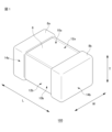
- FIG. 1 is a perspective view showing an outer shape of a laminated ceramic capacitor;
- FIG. 1 is a cross-sectional view schematically showing the internal structure of a laminated ceramic capacitor;
- FIG. 1 is a cross-sectional view schematically showing the internal structure of a laminated ceramic capacitor;
- FIG. A unit cell of a perovskite-type oxide crystal is shown.
- An HAADF image of a cross section of a dielectric ceramic layer is shown.
- An HAADF image of a cross section of a dielectric ceramic layer is shown.
- 4 is a graph showing positional variations of Ba concentration and Ti concentration in the cross section of ⁇ 100 ⁇ grains.
- 4 is a graph showing the positional variation of the Ba concentration difference for one grid.
- 4 is a graph showing the positional variation of the Ti concentration difference for one grid.
- this embodiment A specific embodiment of the present invention (hereinafter referred to as “this embodiment") will be described.
- the present invention is not limited to the following embodiments, and various modifications are possible within the scope of the present invention.
- the laminated ceramic capacitor of the present embodiment has first and second main surfaces facing each other in the thickness direction, first and second side faces facing each other in the width direction, and facing each other in the length direction.
- an element body portion including a plurality of dielectric ceramic layers and a plurality of internal electrode layers laminated in a thickness direction; , and a pair of external electrodes connected to the plurality of internal electrode layers.
- the dielectric ceramic layers contain crystal grains composed of a perovskite-type oxide containing an A-site element and a B-site element.
- S-TEM scanning transmission electron microscope
- the ⁇ 100 ⁇ plane of the perovskite structure is observed.
- the number ratio of ⁇ 100 ⁇ grains in the crystal grains is 4% or more.
- FIG. 1 is a perspective view showing the outline of a laminated ceramic capacitor.
- 2 and 3 are cross-sectional views showing the internal structure of the laminated ceramic capacitor.
- a multilayer ceramic capacitor (100) includes an element body (6) including a plurality of laminated dielectric ceramic layers (2) and a plurality of internal electrode layers (4), and both end surfaces ( and a pair of external electrodes (8a, 8b) provided on the electrodes 14a, 14b).
- the laminated ceramic capacitor (100) and the element body (6) have a substantially rectangular parallelepiped shape.
- a substantially rectangular parallelepiped includes not only a rectangular parallelepiped but also a rectangular parallelepiped with rounded corners and/or edges.
- the multilayer ceramic capacitor (100) and the element body (6) have a first main surface (10a) and a second main surface (10b) facing in the thickness direction T, and a first side surface (12a) facing in the width direction W. ) and second side surfaces (12b), and longitudinally opposite first and second end surfaces (14a) and (14b).
- the thickness direction T refers to the direction in which the plurality of dielectric ceramic layers (2) and the plurality of internal electrode layers (4) are laminated.
- the length direction L refers to a direction perpendicular to the end faces (14a, 14b) on which the external electrodes (8a, 8b) are provided.
- the width direction W is a direction orthogonal to the thickness direction T and the length direction L. As shown in FIG.
- a plane containing the thickness direction T and the width direction W is defined as the WT plane
- a plane containing the width direction W and the length direction L is defined as the LW plane
- a plane containing the length direction L and the thickness direction T is called the LT plane. defined as a surface.
- the external electrodes (8a, 8b) are composed of a first external electrode (8a) provided on the first end face (14a) and a second external electrode (8b) provided on the second end face (14b). be.
- the first external electrode (8a) extends not only to the first end surface (14a) but also to one of the first main surface (10a), the second main surface (10b), the first side surface (12a) and the second side surface (12b). You can turn around to the department.
- the second external electrode (8b) is formed not only on the second end surface (14b) but also on the first main surface (10a), the second main surface (10b), the first side surface (12a) and the second side surface (12b). You can wrap around part of it.
- the first external electrode (8a) and the second external electrode (8b) are not in contact and are electrically separated.
- the internal electrode layers (4) are composed of a plurality of first internal electrode layers (4a) and a plurality of second internal electrode layers (4b).
- the first internal electrode layer (4a) extends to the first end surface (14a) and is electrically connected there to the first external electrode (8a).
- the second internal electrode layer (4b) extends to the second end face (14b) and is electrically connected there to the second external electrode (8b).
- the first internal electrode layer (4a) and the second internal electrode layer (4b) facing each other across the dielectric ceramic layer (2) are not electrically connected. Therefore, when a voltage is applied between the first internal electrode layer (4a) and the second internal electrode layer (4b) through the external electrodes (8a, 8b), charges are accumulated. Accumulated electric charges generate electrostatic capacitance, thereby exhibiting a function as a capacitive element.
- the dimensions of the multilayer ceramic capacitor (100) are not particularly limited. However, it is preferable that the L dimension in the length direction is 0.2 mm or more and 1.2 mm or less, the dimension W in the width direction is 0.1 mm or more and 0.7 mm or less, and the dimension T in the stacking direction is 0.1 mm or more and 0.7 mm or less.
- the dielectric ceramic layer contains crystal grains.
- the crystal grains are particles (main crystal grains) that are the main component of the dielectric ceramic layer, and are composed of a perovskite-type oxide containing an A-site element and a B-site element.
- the dielectric ceramic layer is a sintered polycrystal containing perovskite oxide as a main component.
- a perovskite-type oxide has a composition represented by the general formula: ABO 3 and has a cubic-like crystal structure such as cubic, tetragonal, orthorhombic, and rhombohedral at room temperature.
- A-site element atoms (hereinafter referred to as “A-site atoms”) and B-site element atoms (hereinafter referred to as “B-site atoms”) are ionized to occupy the A-site and B-site of the perovskite structure, respectively.
- A-site elements include elements with relatively large ion sizes, such as barium (Ba), calcium (Ca), and strontium (Sr), and examples of B-site elements include titanium (Ti), zirconium (Zr), and An element with a relatively small ion size such as hafnium (Hf) is exemplified.
- FIG. 4 shows the crystal structure of the perovskite-type oxide.
- An ionized B-site atom such as Ti 4+ (hereinafter “B-site ion”) occupies the body-centered position of the unit cell, and six oxygen ions (O 2 ⁇ ) form the octahedron at the face-centered position. surrounded by
- ionized A-site atoms such as Ba 2+ (hereinafter “A-site ions”) occupy eight corners of the unit cell. Displacement of positively charged A-site ions and/or B-site ions causes dielectric polarization, thereby exhibiting paraelectric or ferroelectric properties at room temperature.
- an ionized atom ion
- an ionized atom may be simply referred to as an "atom".
- A-site elements and B-site elements is not particularly limited as long as the perovskite structure is maintained.
- each of the A-site element and the B-site element may contain only one type of element, or may contain a combination of a plurality of elements.
- the content of the perovskite oxide in the dielectric ceramic layer may be 50% by mass or more, 60% by mass or more, 70% by mass or more, or 80% by mass or more. It may be 90% by mass or more.
- the A-site element comprises barium (Ba) and the B-site element comprises titanium (Ti).
- the perovskite-type oxide may be a barium titanate (BaTiO 3 )-based compound.
- BaTiO3 has a large spontaneous polarization at room temperature. Therefore, it is a ferroelectric that exhibits a high dielectric constant. Therefore, by using the BaTiO 3 -based compound as the main component, it is possible to achieve a further increase in the capacity of the capacitor.
- the BaTiO3 -based compound includes not only BaTiO3 but also BaTiO3 in which part of Ba is replaced with other A-site elements such as Sr and/or Ca, or part of Ti is replaced with Zr and/or Hf. substituted with other B-site elements.
- the molar ratio of Ba in the A-site elements is preferably 70% or more, more preferably 80% or more, and even more preferably 90% or more.
- the ratio of Ti in the B-site elements is preferably 70% or more, more preferably 80% or more, and even more preferably 90% or more in terms of molar ratio.
- the A-site element may contain no components other than Ba and the unavoidable impurity elements, and the B-site element may contain no components other than Ti and the unavoidable impurity elements.
- the unavoidable impurities are components that are unavoidably mixed during the manufacturing process.
- the dielectric ceramic layer may contain other components as additive components in addition to the main component.
- Additives include, but are not limited to, rare earth elements (RE), manganese (Mn), magnesium (Mg), silicon (Si), aluminum (Al), and vanadium (V).
- Rare earth elements (RE) are the group consisting of scandium (Sc) with atomic number 21, yttrium (Y) with atomic number 39, and lanthanum (La) with atomic number 57 to lutetium (Lu) with atomic number 71 in the periodic table.
- the additive component is present in any one of crystal grains, grain boundaries, and triple points. When contained in the crystal grains, it may occupy the A site of the perovskite oxide (ABO 3 ), the B site, or both sites at the same time.
- the dielectric ceramic layers contain ⁇ 100 ⁇ grains as crystal grains.
- the ⁇ 100 ⁇ grains refer to ⁇ 100 ⁇ face is observed. That is, part or all of the crystal grains are ⁇ 100 ⁇ grains. Also, it is sufficient that ⁇ 100 ⁇ planes are observed in at least a part of the ⁇ 100 ⁇ grains.
- the cross section is a plane including the thickness direction, that is, the stacking direction of the dielectric ceramic layers and the internal electrode layers.
- the cross section can also be referred to as a plane whose perpendicular is perpendicular to the thickness direction, such as the LT plane and the WT plane.
- the ⁇ 100 ⁇ plane is a crystal lattice plane represented by the Miller index, and includes (100) plane, (010) plane, (001) plane, (-100) plane, (0-10) plane, (00- 1) Includes 6 faces.
- a scanning transmission electron microscope is a device that scans a focused microincidence probe over a sample and converts the transmitted electrons into luminance signals to observe fine structures. Due to recent advances in equipment, the spatial resolution has improved to 50 pm or less, and the detection sensitivity has reached the level of single atoms.
- various images can be observed using electrons scattered from the sample.
- an image obtained by detecting electrons with a scattering angle larger than the convergence angle of the incident probe using an annular detector is an annular dark-field (ADF) image.
- ADF annular dark-field
- an image with a particularly large scattering angle is a High Angle Annular Dark-Field (HAADF) image. Since the intensity of HAADF corresponds to the atomic number Z, the HAADF image has excellent element discrimination ability. Therefore, by analyzing the HAADF image in particular, the position information of the element can be evaluated with high accuracy.
- the presence or absence of ⁇ 100 ⁇ grains and their ratio can be examined by obtaining an ADF image, an HAADF image and/or an electron beam diffraction pattern for the central portion of the crystal grains constituting the dielectric ceramic layer and analyzing them.
- an ADF image or HAADF image of a specific grain central portion is obtained by a nano beam electron diffraction (NBD) method.
- NBD nano beam electron diffraction
- the grain when the ⁇ 100 ⁇ plane based on the arrangement of atoms constituting the perovskite oxide is observed, the grain can be determined to be a ⁇ 100 ⁇ grain.
- an electron diffraction pattern may be obtained by the NBD method, and when only periodic patterns based on ⁇ 100 ⁇ planes are present in this electron diffraction pattern, the grain may be determined to be a ⁇ 100 ⁇ grain.
- the S-TEM observation is performed on the cross section including the thickness direction of the dielectric ceramic layer. More specifically, at the center of the plane (WT plane) located at the center in the length direction (L direction) of the dielectric ceramic layer and including the width direction (W direction) and thickness direction (T direction) It is preferable to observe the area. Observation may be performed on a region having a field of view of 10 ⁇ m ⁇ 10 ⁇ m or a region containing 200 crystal grains. In the S-TEM observation, the microscope axis is fixed in a direction substantially perpendicular to the cross section of the dielectric ceramic layer, and in that state, the cross section of the dielectric ceramic layer is tilted within a range of ⁇ 5°.
- Grains in which ⁇ 100 ⁇ planes are observed within this range ( ⁇ 5°) of inclination angle are defined as ⁇ 100 ⁇ grains.
- ⁇ 100 ⁇ grains are those whose ⁇ 100 ⁇ faces are exposed within a range of ⁇ 5° with respect to the vertical axis of the cross section of the dielectric ceramic layer.
- FIG. 5 shows an example of a cross-sectional HAADF image of ⁇ 100 ⁇ grains contained in the dielectric ceramic layers of the multilayer ceramic capacitor of this embodiment.
- This laminated ceramic capacitor uses barium titanate (BaTiO 3 ) for dielectric ceramic layers.
- BaTiO 3 barium titanate
- luminous points based on Ba and luminous points based on Ti are observed, and these luminescent points each constitute a lattice-like atomic (ion) arrangement.
- the Ba bright spot has a higher brightness than the Ti bright spot. This is because the atomic weight of Ba is larger than that of Ti.
- the number ratio of ⁇ 100 ⁇ grains in the crystal grains is 4% or more in the above-described cross section, that is, the cross section including the thickness direction of the dielectric ceramic layers.
- the dielectric constant of the dielectric ceramic layer can be increased.
- the orientation state of the crystal grains contained in the dielectric ceramic layer is related. That is, in the cubic crystal structure of the perovskite-type oxide crystal that constitutes the crystal grains, all six planes, such as the (100) plane that constitutes the ⁇ 100 ⁇ plane, are equivalent.
- the number ratio is preferably 10% or more, more preferably 15% or more, and even more preferably 20% or more.
- the upper limit of the number ratio is not particularly limited.
- the ⁇ 100 ⁇ grains have an atomic arrangement region, and the average area ratio thereof is 10% or more in the ⁇ 100 ⁇ grain cross section.
- the atomic arrangement region is a region where the atomic arrangement of the perovskite oxide, that is, the ordered arrangement of A-site atoms and B-site atoms, is observed by S-TEM observation.
- a ⁇ 100 ⁇ grain may have a region where ⁇ 100 ⁇ planes are observed in the center, that is, a region where atoms are arranged, and a surrounding area where atoms are not arranged where ⁇ 100 ⁇ planes are not observed. .
- the ⁇ 100 ⁇ plane may be observed at the central portion and the ⁇ 100 ⁇ plane may not be observed at the outer peripheral portion.
- a regular arrangement of the A-site atoms and B-site atoms constituting the perovskite-type oxide is observed in the atomic arrangement region, whereas no regular arrangement is observed in the non-atom arrangement region. This is because, in the non-arranged region of atoms, the lattice distortions of the A-site atoms and B-site atoms are particularly large, indicating structural irregularities.
- the average area ratio of the atomic arrangement region is more preferably 20% or more, still more preferably 30% or more, and particularly preferably 40% or more.
- the upper limit of the average area ratio is not particularly limited. However, it is typically 50% or less.
- the area ratio of the atomic arrangement region can be obtained by the S-TEM observation described above. That is, for each ⁇ 100 ⁇ grain, an ADF image or HAADF image of the entire grain is obtained by the NBD method, and a region where atomic arrangement is observed in these images (atomic arrangement region) is determined. Then, the area ratio of the atomic arrangement region in the cross section of the grain is calculated, and the average value thereof can be obtained as the average area ratio.
- the ⁇ 100 ⁇ grain in the cross section described above has an atomic distribution region at one or more atomic positions within the grain, and the area of this atomic distribution region (S ⁇ c ⁇ 2% ) is 0.050 nm 2 or less.
- the atom distribution region is a measure of the spread of the atom position distribution centering on the lattice point.
- the atomic concentration difference ( ⁇ c) of the A-site element or B-site element that exists inside the unit cell centered on one lattice point and corresponds to this lattice point is 2 atm. % or less.
- the atomic concentration difference ( ⁇ c) is the difference (c max ⁇ c).
- the concentration of atoms that should occupy this lattice point is maximized at the lattice point and decreases as the distance from the lattice point increases. Therefore, if the size of the atomic distribution region can be estimated quantitatively, the spread of the atomic position distribution can be evaluated.
- the high-temperature load life of the multilayer ceramic capacitor becomes longer, and as a result, the reliability can be improved.
- the details of the mechanism are unknown, it is speculated as follows.
- a real crystal has many lattice defects such as oxygen vacancies and atomic defects.
- oxygen vacancies are considered to be a factor in shortening the high temperature load life of the multilayer ceramic capacitor.
- the area is preferably 0.045 nm 2 or less, more preferably 0.040 nm 2 or less, even more preferably 0.035 nm 2 or less, particularly preferably 0.030 nm 2 or less, and most preferably 0.023 nm 2 or less.
- the lower limit is not particularly limited. For example, the area is 0.001 nm 2 or more.
- FIG. 5 shows an example of a cross-sectional HAADF image of ⁇ 100 ⁇ grains contained in the dielectric ceramic layers of the multilayer ceramic capacitor of this embodiment.
- FIG. 6 shows a cross-sectional HAADF image of a laminated ceramic capacitor obtained by a conventional technique.
- barium titanate BaTiO 3
- luminescent spots based on Ba and luminescent spots based on Ti are observed, and these luminescent spots each constitute a lattice-like atomic (ion) arrangement.
- the ⁇ 100 ⁇ grains of the present embodiment have a small bright spot size, whereas the ⁇ 100 ⁇ grains of the prior art have a large bright spot size. This is because, in the ⁇ 100 ⁇ grains of the present embodiment, the ionized Ba and Ti atom distribution regions are concentrated near the lattice points, whereas in the ⁇ 100 ⁇ grains of the prior art, the Ba and Ti lattices are distorted. is generated, and the atomic distribution region is expanded.
- FIG. 7 shows the positional variation of Ba concentration and Ti concentration in the ⁇ 100 ⁇ grain cross section. This is obtained by performing compositional analysis by energy dispersive X-ray spectroscopy (EDX) along a straight line on the ⁇ 100 ⁇ grain cross section and obtaining the atomic concentration obtained by this analysis as a function of position (distance).
- EDX energy dispersive X-ray spectroscopy
- Ba concentration and Ti concentration fluctuate periodically. Reflecting the positions of Ba and Ti in the crystal, the Ti concentration is the lowest at the position where the Ba concentration is maximum (peak), and the Ti concentration is highest at the position where the Ba concentration is minimum.
- the positional variation of the Ba concentration difference is sharp. That is, away from the origin, the Ba concentration rapidly decreases.
- the ⁇ 100 ⁇ grains of the prior art have a broad Ba concentration difference. This tendency reflects the bright spot size in the HAADF image. Therefore, in the graph of FIG. 8, the distance from the origin is obtained for the position where the Ba concentration difference ( ⁇ c) is 2 atm %, and the area of a circle whose radius is this distance is calculated. It can be regarded as the area (S ⁇ c ⁇ 2% ).
- a horizontal line is drawn along the horizontal axis when the Ba concentration difference ( ⁇ c) is 2 atm %. Then, the distances from the vertical axis to two points (a point and b point) where this line intersects the Ba concentration difference graph are read and defined as d a and d b , respectively. Then, the area of the atomic distribution region (S ⁇ c ⁇ 2% ) can be obtained according to the following formulas (2) and (3).
- the thickness of the dielectric ceramic layer is preferably 1.0 ⁇ m or less, particularly preferably 0.4 ⁇ m or less. By thinning the dielectric ceramic layer, it becomes possible to increase the capacity of the multilayer ceramic capacitor. However, if the dielectric ceramic layer is excessively thin, it becomes difficult to suppress deterioration in insulating properties.
- the thickness of the dielectric ceramic layer is typically 0.15 ⁇ m or more.
- the internal electrode layers contain a conductive metal.
- a conductive metal such as nickel (Ni), copper (Cu), silver (Ag), palladium (Pd), and alloys containing these may be used as the conductive metal.
- base metals such as Ni and Cu are preferable, and Ni is particularly preferable.
- the internal electrode layers may contain components other than the conductive metal.
- Other components may include ceramic components that act as co-materials. Examples of ceramic components include perovskite-type oxides such as BaTiO 3 -based compounds contained in the dielectric ceramic layer.
- the thickness of the internal electrode layer is preferably 0.20 ⁇ m or more and 0.80 ⁇ m or less. By setting the thickness of the internal electrode layer to 0.20 ⁇ m or more, defects such as electrode disconnection are suppressed. Further, by setting the thickness to 0.80 ⁇ m or less, it becomes possible to suppress the decrease in the ratio of the dielectric ceramic layer in the capacitor and the resulting decrease in capacitance.
- the number of internal electrode layers is preferably 15 or more and 700 or less.
- a known configuration can be adopted as the external electrode.
- it may be a laminated structure composed of an underlying layer, a first plated layer, and a second plated layer from the end face side of the laminated ceramic capacitor.
- the underlayer contains metal such as nickel (Ni) or copper (Cu).
- ceramic powder may be included in addition to the metal as a common material.
- the first plating layer is, for example, a nickel (Ni) plating layer.
- the second plating layer is, for example, a tin (Sn) plating layer.
- a conductive resin layer may be provided between the base layer and the first plating layer.
- the conductive resin layer is a layer containing conductive metal particles such as copper (Cu), silver (Ag) and nickel (Ni), and resin.
- the form of the external electrode is not limited as long as it is electrically connected to the internal electrode layer and functions as an external input/output terminal.
- a manufacturing method of the multilayer ceramic capacitor of the present embodiment is not limited as long as it satisfies the requirements described above. However, it is preferably manufactured by the following method.
- a preferred manufacturing method includes the following steps; a step of producing a green sheet containing at least a dielectric material (green sheet producing step); A step of obtaining a sheet (electrode pattern forming step), a step of laminating and crimping a plurality of green sheets to obtain a laminated block (lamination step), and a step of cutting the obtained laminated block to obtain a laminated chip (cutting step).
- a step of subjecting the obtained laminated chip to a binder removal treatment and a firing treatment to obtain an element body (firing step), and a step of forming external electrodes on the obtained element body (external electrode forming step). , provided. Details of each step are described below.
- a green sheet is a precursor of a dielectric ceramic layer of a capacitor, and contains a main component raw material and an additive component raw material of the dielectric ceramic layer.
- the production of the green sheet may be performed by a known method, and is not particularly limited.
- a dielectric raw material is prepared by mixing additive component raw materials with a main component raw material, a binder and a solvent are added to and mixed with the obtained dielectric raw material to form a slurry, and a green sheet is formed from the obtained slurry.
- Powders of perovskite-type oxides such as BaTiO 3 -based compounds can be used as the raw material for the main component.
- the perovskite-type oxide powder may be synthesized by a known method such as a solid-phase reaction method, hydrothermal synthesis method, alkoxide method, or the like.
- known additives such as oxides, carbonates, hydroxides, nitrates, organic acid salts, alkoxides and/or chelate compounds of additive components (RE, Mn, Mg, Si, Al, and V) can be used as raw materials for additive components.
- a ceramic raw material may be used.
- Raw material mixing may be performed by a known method, for example, a method of wet-mixing and pulverizing the weighed main component raw material and additive component raw material together with grinding media and pure water using a ball mill. If wet mixing is used, the resulting mixture may be dried.
- Slurrying may also be performed by a known method, and the dielectric raw material may be mixed with an organic binder and an organic solvent.
- the organic binder a known binder such as a polyvinyl brural binder may be used.
- an organic solvent a known solvent such as toluene or ethanol may be used.
- Additives such as plasticizers may be added to the slurry as needed.
- the molding of the green sheet may also be performed by a known method such as a doctor blade method or a lip method.
- a conductive paste is applied to the surface of a green sheet to produce a green sheet having an internal electrode pattern formed thereon.
- the internal electrode patterns become internal electrode layers after firing.
- a conductive material such as nickel (Ni), copper (Cu), silver (Ag), palladium (Pd), or an alloy containing these may be used.
- a ceramic component that acts as a common material may also be added to the conductive paste.
- the ceramic component the raw material of the main component of the dielectric ceramic layer can be used.
- Application of the conductive paste may be performed by a known technique such as screen printing or gravure printing.
- ⁇ Lamination process> In the lamination step, a plurality of green sheets are laminated and pressure-bonded to produce a laminated block. In this case, green sheets with internal electrode patterns formed thereon are used, but some green sheets without internal electrode patterns may also be used. Lamination and crimping may be performed by a known method.
- the obtained laminated block is cut to produce laminated chips. Cutting may be performed so that chips of a predetermined size are obtained and at least a portion of the internal electrode pattern is exposed on the end face of the laminated chip.
- the laminated chip thus obtained is subjected to binder removal treatment and firing treatment to fabricate the element body.
- the firing process co-sinters the green sheets and the internal electrode patterns to form dielectric ceramic layers and internal electrode layers, respectively.
- the conditions for the binder removal treatment may be determined according to the types of organic binders contained in the green sheets and internal electrode patterns.
- the firing treatment may be performed at a temperature at which the laminated chip is sufficiently densified. For example, the temperature may be kept at 1200° C. or higher and 1300° C. or lower for 0 minute or longer and 30 minutes or shorter.
- the firing is carried out in an atmosphere in which the perovskite-type oxide, which is the main component, is not reduced and the oxidation of the conductive metal is suppressed.
- it may be carried out in an N 2 —H 2 —H 2 O airflow with an oxygen partial pressure of 10 ⁇ 10 to 10 ⁇ 12 MPa.
- annealing may be performed after firing.
- a dielectric material having a relatively high degree of crystallinity such as BaTiO 3 having a c-axis/a-axis ratio of 1.0085 or more, is used as the main component raw material.
- the laminated chip is held at a predetermined temperature for a predetermined time, and after the firing process, pressure is applied in the thickness direction by annealing. By performing annealing at a predetermined temperature while applying pressure in the stacking direction, stress is applied to crystal grains with a relatively high degree of crystallinity.
- the holding temperature is preferably 800° C. or more and 1000° C. or less, and the holding time (pressure application time) is preferably 30 minutes or more and 120 minutes or less.
- the applied pressure is preferably 1 MPa or more and 120 MPa or less. If the applied pressure is less than 1 MPa, the rearrangement of crystal grains becomes insufficient due to insufficient stress. Therefore, in the finally obtained multilayer ceramic capacitor, the proportion of ⁇ 100 ⁇ grains in the dielectric ceramic layers cannot be increased. On the other hand, if the pressure exceeds 120 MPa, the applied pressure becomes excessively high, which may cause defects such as cracking or chipping of the laminated chip.
- external electrodes are formed on the obtained element body. Formation of the external electrodes may be performed by a known method. For example, a conductive paste containing a metal such as silver (Ag), copper (Cu), and/or nickel (Ni) may be applied and baked on the end face of the element body where the internal electrodes are drawn out and exposed. Alternatively, a technique may be used in which a conductive paste is applied to both end surfaces of the laminated chip before firing, and then firing treatment is performed. Further, the formed electrode may be used as a base layer, and a plating film such as nickel (Ni) or tin (Sn) may be formed thereon. A multilayer ceramic capacitor is manufactured through the formation of the external electrodes in this way.
- a conductive paste containing a metal such as silver (Ag), copper (Cu), and/or nickel (Ni) may be applied and baked on the end face of the element body where the internal electrodes are drawn out and exposed.
- a technique may be used in which a conductive paste is applied to both end
- Bam TiO 3 powder was prepared as a main component raw material.
- m is the A/B molar ratio of the perovskite oxide (ABO 3 ), that is, the Ba/Ti molar ratio.
- ABO 3 perovskite oxide
- Ba/Ti molar ratio As the BamTiO 3 powder, powder having a particle diameter D50 of 140 nm, a perovskite structure with a c-axis/a-axis ratio of 1.0090 and m of 1.005 was used.
- the prepared BamTiO 3 powder was weighed and wet-mixed by a ball mill to crush aggregates.
- raw materials for additive components (Dy, Mg, Mn, Si, Al, V) were weighed.
- Raw materials for additive components include dysprosium oxide ( Dy2O3 ), magnesium carbonate ( MgCO3 ), manganese carbonate ( MnCO3 ), silicon oxide ( SiO2 ), aluminum oxide ( Al2O3 ), and vanadium oxide (V2 ) . O 5 ) was used.
- Dy 1.0 mol part, Mg: 0.03 mol part, Mn: 0.1 mol part, Si: 0.8 mol part, Al: 0.08 mol part and V: 0.08 mol part.
- the additive component raw materials were added to the main component raw materials, wet-mixed using a ball mill, dried and heat-treated to obtain dielectric raw materials.
- a polyvinyl butyral-based binder and ethanol as an organic solvent were added to the obtained dielectric raw material, and wet-mixed by a ball mill for a predetermined time to prepare a slurry. This slurry was formed into a sheet to produce a green sheet for a dielectric ceramic layer.
- a conductive paste mainly composed of Ni was screen-printed on the surface of the obtained green sheet to form a pattern of conductive paste layers that would become internal electrode layers.
- a plurality of green sheets each having a conductive paste layer formed thereon were laminated, and green sheets without a conductive paste layer formed thereon were placed above and below the green sheets, and the whole was pressed together to produce a laminated block.
- the obtained laminated block was cut with a dicing saw into laminated chips. Lamination was performed so that the ends from which the conductive paste layers were drawn out were alternated. Also, the cutting was performed so that the conductive paste layer was exposed on the side surface.
- a side margin green sheet (side margin green body) was pasted on both sides of the cut laminated chip where the conductive paste layer was exposed. Side margin green sheets were produced in the same manner as the dielectric ceramic layer green sheets.
- the laminated chip with the side margin green body attached was placed in an N 2 —H 2 O—H 2 stream at an oxygen partial pressure of 1.8 ⁇ 10 ⁇ 9 to 8.7 ⁇ 10 ⁇ 10 MPa at a temperature elevation rate of 20° C. /sec, maximum temperature 1260°C x 0.5 hours. After sintering, it was annealed in an atmosphere of oxygen partial pressure of 1.0 ⁇ 10 ⁇ 12 to 10 ⁇ 15 MPa and 800 to 1000° C. while applying pressure in the stacking direction to obtain a multilayer ceramic capacitor body.
- a conductive paste containing copper (Cu) as a main component was applied to the end faces of the element obtained by firing where the internal electrode layers were drawn out. After that, the applied conductive paste was baked at 900° C. to form a base layer for the external electrodes. Further, Ni plating and Sn plating were performed in this order on the surface layer of the underlayer by wet plating. Thus, a laminated ceramic capacitor was produced.
- Cu copper
- the manufactured multilayer ceramic capacitor had a length L dimension of 0.4 mm, a width direction W dimension of 0.2 mm, and a thickness direction T dimension of 0.2 mm.
- the dielectric layers had a thickness of 0.5 ⁇ m
- the internal electrode layers had a thickness of 0.4 ⁇ m
- the number of dielectric ceramic layers was 150.
- ⁇ Dielectric properties> The capacitance C of the multilayer ceramic capacitor was measured using an automatic bridge type measuring machine. The measurement was performed under the conditions of a temperature of 25° C., an effective voltage of 0.5 Vrms, and a frequency of 1 kHz. Then, using the capacitance C, the dielectric constant ( ⁇ r ) of the dielectric ceramic layer was obtained. Also, the relative permittivity value of Comparative Example 1 was used as a reference, and the relative permittivity ratio ( ⁇ r ratio) was obtained.
- S-TEM scanning transmission electron microscope
- a thin film was processed by a focused ion beam (FIB) method to prepare an observation sample.
- FIB focused ion beam
- a thin sample having a thickness of 100 nm or less and having a plane (WT plane) including the width direction and the thickness direction was taken out from the central portion of the laminated ceramic capacitor in the length direction (L direction).
- This flake sample had a thickness smaller than the radius of the grains contained in the sample.
- the EDX device attached to the S-TEM was used to obtain the Ba concentration and Ti concentration in the cross section of the ⁇ 100 ⁇ grain as a function of distance (positional variation) and graphed.
- An example of the obtained graph is shown in FIG.
- point A is a point where the positional variation of Ba concentration is relatively sharp
- point B is a point where it is relatively broad
- point C is a point where the positional variation of the Ti concentration is relatively sharp
- point D is a point where it is relatively broad. It is conceivable that the locations with sharp positional fluctuations have small lattice distortions, while the locations with broad positional fluctuations have large lattice distortions.
- FIGS. 8 and 9 show the results obtained for BaTiO 3 produced by the conventional technique.
- each area (S ⁇ c ⁇ 2% ) of the Ba atom distribution region and the Ti atom distribution region was determined. Specifically, a line with a density difference ( ⁇ c) of 2 atm % was drawn horizontally on the horizontal axis. Then, the distances from the vertical axis to two points (a point and b point) where this line intersects the density difference graph were read and defined as d a and d b , respectively. Then, the area of the atomic distribution region (S ⁇ c ⁇ 2% ) was calculated according to the following formulas (2) and (3). The area of the atomic distribution region was calculated for all the detected ⁇ 100 ⁇ particles, and the average value of 10 particles selected in ascending order of area was obtained.
- Table 1 summarizes the pressure conditions during firing and the characteristics of the dielectric ceramic layers for Comparative Examples 1 and 2 and Examples 1 to 22.
- Table 1 shows the area of the Ba atom distribution region (S ⁇ c ⁇ 2% ). The area of the Ti atom distribution region was almost the same as the value for Ba.
- the proportion of ⁇ 100 ⁇ grains increased as the pressure applied in the firing process during the manufacturing of the multilayer ceramic capacitor increased and the application time increased, resulting in a higher relative permittivity ( ⁇ r ).
- the dielectric constant is 2920 or more
- the dielectric constant is 3220. That was it.
- Examples 5 to 9 and 13 to 22 with an area ratio of 10% or more had an MTTF of 25 hours or more
- Examples 8, 9 and 14 to 22 with an area ratio of 30% or more had an MTTF of 31 hours or more.
Landscapes
- Engineering & Computer Science (AREA)
- Power Engineering (AREA)
- Chemical & Material Sciences (AREA)
- Ceramic Engineering (AREA)
- Manufacturing & Machinery (AREA)
- Microelectronics & Electronic Packaging (AREA)
- Inorganic Chemistry (AREA)
- Materials Engineering (AREA)
- Structural Engineering (AREA)
- Organic Chemistry (AREA)
- Ceramic Capacitors (AREA)
- Fixed Capacitors And Capacitor Manufacturing Machines (AREA)
Priority Applications (5)
| Application Number | Priority Date | Filing Date | Title |
|---|---|---|---|
| KR1020247009442A KR102840601B1 (ko) | 2021-09-28 | 2022-09-22 | 적층 세라믹 콘덴서 |
| CN202280063072.3A CN117957626A (zh) | 2021-09-28 | 2022-09-22 | 层叠陶瓷电容器 |
| JP2023551420A JP7700867B2 (ja) | 2021-09-28 | 2022-09-22 | 積層セラミックコンデンサ |
| US18/608,996 US12512266B2 (en) | 2021-09-28 | 2024-03-19 | Multilayer ceramic capacitor |
| US19/398,331 US20260088222A1 (en) | 2021-09-28 | 2025-11-24 | Multilayer ceramic capacitor |
Applications Claiming Priority (2)
| Application Number | Priority Date | Filing Date | Title |
|---|---|---|---|
| JP2021158283 | 2021-09-28 | ||
| JP2021-158283 | 2021-09-28 |
Related Child Applications (1)
| Application Number | Title | Priority Date | Filing Date |
|---|---|---|---|
| US18/608,996 Continuation US12512266B2 (en) | 2021-09-28 | 2024-03-19 | Multilayer ceramic capacitor |
Publications (1)
| Publication Number | Publication Date |
|---|---|
| WO2023054183A1 true WO2023054183A1 (ja) | 2023-04-06 |
Family
ID=85782580
Family Applications (1)
| Application Number | Title | Priority Date | Filing Date |
|---|---|---|---|
| PCT/JP2022/035442 Ceased WO2023054183A1 (ja) | 2021-09-28 | 2022-09-22 | 積層セラミックコンデンサ |
Country Status (5)
| Country | Link |
|---|---|
| US (2) | US12512266B2 (https=) |
| JP (1) | JP7700867B2 (https=) |
| KR (1) | KR102840601B1 (https=) |
| CN (1) | CN117957626A (https=) |
| WO (1) | WO2023054183A1 (https=) |
Citations (2)
| Publication number | Priority date | Publication date | Assignee | Title |
|---|---|---|---|---|
| JP2015062216A (ja) * | 2013-08-23 | 2015-04-02 | Tdk株式会社 | 積層型セラミック電子部品 |
| US20200266264A1 (en) * | 2019-02-14 | 2020-08-20 | Samsung Electronics Co., Ltd. | Single crystal material and method of forming the same and stacked structure and ceramic electronic component and device |
Family Cites Families (9)
| Publication number | Priority date | Publication date | Assignee | Title |
|---|---|---|---|---|
| JP4110978B2 (ja) * | 2003-01-24 | 2008-07-02 | 株式会社村田製作所 | 誘電体セラミックおよびその製造方法ならびに積層セラミックコンデンサ |
| TW200706513A (en) * | 2005-04-27 | 2007-02-16 | Murata Manufacturing Co | Dielectric ceramic, process for producing the same, and laminated ceramic capacitor |
| KR101581809B1 (ko) | 2012-06-29 | 2015-12-31 | 다이요 유덴 가부시키가이샤 | 적층 세라믹 콘덴서 |
| JP2014084267A (ja) | 2012-10-26 | 2014-05-12 | Kyocera Corp | 誘電体磁器および積層セラミックコンデンサ |
| JP5857116B2 (ja) | 2014-12-15 | 2016-02-10 | 太陽誘電株式会社 | 積層セラミックコンデンサ及びその製造方法 |
| KR102392041B1 (ko) * | 2017-03-10 | 2022-04-27 | 삼성전자주식회사 | 유전체, 그 제조 방법, 이를 포함하는 유전체 소자 및 전자 소자 |
| KR102363288B1 (ko) * | 2017-03-10 | 2022-02-14 | 삼성전자주식회사 | 유전체, 그 제조 방법, 이를 포함하는 유전체 소자 및 전자 소자 |
| KR102325821B1 (ko) * | 2017-03-31 | 2021-11-11 | 삼성전자주식회사 | 2차원 페로브스카이트 소재, 이를 포함하는 유전체 및 적층형 커패시터 |
| JP7838895B2 (ja) * | 2022-03-07 | 2026-04-01 | 太陽誘電株式会社 | 積層セラミック電子部品 |
-
2022
- 2022-09-22 CN CN202280063072.3A patent/CN117957626A/zh active Pending
- 2022-09-22 JP JP2023551420A patent/JP7700867B2/ja active Active
- 2022-09-22 WO PCT/JP2022/035442 patent/WO2023054183A1/ja not_active Ceased
- 2022-09-22 KR KR1020247009442A patent/KR102840601B1/ko active Active
-
2024
- 2024-03-19 US US18/608,996 patent/US12512266B2/en active Active
-
2025
- 2025-11-24 US US19/398,331 patent/US20260088222A1/en active Pending
Patent Citations (2)
| Publication number | Priority date | Publication date | Assignee | Title |
|---|---|---|---|---|
| JP2015062216A (ja) * | 2013-08-23 | 2015-04-02 | Tdk株式会社 | 積層型セラミック電子部品 |
| US20200266264A1 (en) * | 2019-02-14 | 2020-08-20 | Samsung Electronics Co., Ltd. | Single crystal material and method of forming the same and stacked structure and ceramic electronic component and device |
Also Published As
| Publication number | Publication date |
|---|---|
| US12512266B2 (en) | 2025-12-30 |
| US20240222021A1 (en) | 2024-07-04 |
| CN117957626A (zh) | 2024-04-30 |
| KR102840601B1 (ko) | 2025-07-31 |
| JPWO2023054183A1 (https=) | 2023-04-06 |
| JP7700867B2 (ja) | 2025-07-01 |
| US20260088222A1 (en) | 2026-03-26 |
| KR20240042221A (ko) | 2024-04-01 |
Similar Documents
| Publication | Publication Date | Title |
|---|---|---|
| JP7124528B2 (ja) | 積層セラミック電子部品 | |
| KR102587765B1 (ko) | 적층 세라믹 콘덴서 및 그 제조 방법 | |
| JP7528830B2 (ja) | 積層セラミックコンデンサ | |
| KR102520018B1 (ko) | 적층 세라믹 콘덴서 및 그 제조 방법 | |
| JP7363701B2 (ja) | 誘電体組成物および積層セラミック電子部品 | |
| JPH11273985A (ja) | 誘電体セラミックおよびその製造方法、ならびに、積層セラミック電子部品およびその製造方法 | |
| US20250259790A1 (en) | Multilayer ceramic capacitor | |
| CN117836882A (zh) | 层叠陶瓷电容器 | |
| US12482604B2 (en) | Multilayer ceramic capacitor | |
| US20240274357A1 (en) | Multilayer ceramic capacitor | |
| US20260074114A1 (en) | Multilayer ceramic capacitor including dielectric ceramic layers including rare earth element concentration regions | |
| CN113628879A (zh) | 电介质、电子器件和层叠陶瓷电容器 | |
| KR102491421B1 (ko) | 적층 세라믹 콘덴서 및 그 제조 방법 | |
| JP7700867B2 (ja) | 積層セラミックコンデンサ | |
| WO2023054378A1 (ja) | 積層セラミックコンデンサ | |
| US20250385046A1 (en) | Multilayer ceramic capacitor | |
| WO2026070751A1 (ja) | 積層セラミックコンデンサ | |
| WO2026070752A1 (ja) | 積層セラミックコンデンサ用セラミック粉末、積層セラミックコンデンサ用セラミック粉末の製造方法、及び積層セラミックコンデンサの製造方法 | |
| WO2026070746A1 (ja) | 積層セラミックコンデンサ | |
| WO2026070745A1 (ja) | 積層セラミックコンデンサ | |
| WO2026070749A1 (ja) | 積層セラミックコンデンサ | |
| WO2025070580A1 (ja) | 積層セラミックコンデンサ |
Legal Events
| Date | Code | Title | Description |
|---|---|---|---|
| 121 | Ep: the epo has been informed by wipo that ep was designated in this application |
Ref document number: 22876050 Country of ref document: EP Kind code of ref document: A1 |
|
| WWE | Wipo information: entry into national phase |
Ref document number: 2023551420 Country of ref document: JP |
|
| WWE | Wipo information: entry into national phase |
Ref document number: 202280063072.3 Country of ref document: CN |
|
| NENP | Non-entry into the national phase |
Ref country code: DE |
|
| 122 | Ep: pct application non-entry in european phase |
Ref document number: 22876050 Country of ref document: EP Kind code of ref document: A1 |