WO2023053967A1 - 電力変換装置及び電力変換装置の製造方法 - Google Patents
電力変換装置及び電力変換装置の製造方法 Download PDFInfo
- Publication number
- WO2023053967A1 WO2023053967A1 PCT/JP2022/034413 JP2022034413W WO2023053967A1 WO 2023053967 A1 WO2023053967 A1 WO 2023053967A1 JP 2022034413 W JP2022034413 W JP 2022034413W WO 2023053967 A1 WO2023053967 A1 WO 2023053967A1
- Authority
- WO
- WIPO (PCT)
- Prior art keywords
- heat sink
- substrate
- housing
- power converter
- circuit components
- Prior art date
- Legal status (The legal status is an assumption and is not a legal conclusion. Google has not performed a legal analysis and makes no representation as to the accuracy of the status listed.)
- Ceased
Links
Images




Classifications
-
- H—ELECTRICITY
- H01—ELECTRIC ELEMENTS
- H01G—CAPACITORS; CAPACITORS, RECTIFIERS, DETECTORS, SWITCHING DEVICES, LIGHT-SENSITIVE OR TEMPERATURE-SENSITIVE DEVICES OF THE ELECTROLYTIC TYPE
- H01G2/00—Details of capacitors not covered by a single one of groups H01G4/00-H01G11/00
- H01G2/08—Cooling arrangements; Heating arrangements; Ventilating arrangements
-
- H—ELECTRICITY
- H01—ELECTRIC ELEMENTS
- H01G—CAPACITORS; CAPACITORS, RECTIFIERS, DETECTORS, SWITCHING DEVICES, LIGHT-SENSITIVE OR TEMPERATURE-SENSITIVE DEVICES OF THE ELECTROLYTIC TYPE
- H01G2/00—Details of capacitors not covered by a single one of groups H01G4/00-H01G11/00
- H01G2/10—Housing; Encapsulation
-
- H—ELECTRICITY
- H02—GENERATION; CONVERSION OR DISTRIBUTION OF ELECTRIC POWER
- H02M—APPARATUS FOR CONVERSION BETWEEN AC AND AC, BETWEEN AC AND DC, OR BETWEEN DC AND DC, AND FOR USE WITH MAINS OR SIMILAR POWER SUPPLY SYSTEMS; CONVERSION OF DC OR AC INPUT POWER INTO SURGE OUTPUT POWER; CONTROL OR REGULATION THEREOF
- H02M7/00—Conversion of AC power input into DC power output; Conversion of DC power input into AC power output
- H02M7/003—Constructional details, e.g. physical layout, assembly, wiring or busbar connections
-
- H—ELECTRICITY
- H02—GENERATION; CONVERSION OR DISTRIBUTION OF ELECTRIC POWER
- H02M—APPARATUS FOR CONVERSION BETWEEN AC AND AC, BETWEEN AC AND DC, OR BETWEEN DC AND DC, AND FOR USE WITH MAINS OR SIMILAR POWER SUPPLY SYSTEMS; CONVERSION OF DC OR AC INPUT POWER INTO SURGE OUTPUT POWER; CONTROL OR REGULATION THEREOF
- H02M7/00—Conversion of AC power input into DC power output; Conversion of DC power input into AC power output
- H02M7/42—Conversion of DC power input into AC power output without possibility of reversal
- H02M7/44—Conversion of DC power input into AC power output without possibility of reversal by static converters
- H02M7/48—Conversion of DC power input into AC power output without possibility of reversal by static converters using discharge tubes with control electrode or semiconductor devices with control electrode
-
- H—ELECTRICITY
- H01—ELECTRIC ELEMENTS
- H01G—CAPACITORS; CAPACITORS, RECTIFIERS, DETECTORS, SWITCHING DEVICES, LIGHT-SENSITIVE OR TEMPERATURE-SENSITIVE DEVICES OF THE ELECTROLYTIC TYPE
- H01G4/00—Fixed capacitors; Processes of their manufacture
- H01G4/32—Wound capacitors
Definitions
- the present disclosure relates to a power converter and a method for manufacturing the power converter.
- Patent Document 1 Japanese Patent Application Laid-Open No. 2016-66666 (Patent Document 1) describes a capacitor.
- the capacitor described in Patent Document 1 has a case, a capacitor element, electrode plates, mold resin, and a lid.
- a capacitor element and an electrode plate are housed in a case.
- the lead terminals of the capacitor element are electrically connected to the electrode plates.
- Mold resin is filled in the case.
- the lid is attached to the opening of the case.
- the heat generated in the capacitor element is transferred to the lid through the lead terminals and electrode plates, and radiated from the protrusions of the lid. Therefore, the capacitor described in Patent Document 1 has a large thermal resistance, and the temperature rise of the capacitor element increases.
- the present disclosure has been made in view of the problems of the prior art as described above. More specifically, the present disclosure provides a power conversion device capable of suppressing temperature rise of circuit components.
- a power conversion device includes a housing, a plurality of circuit components housed in the housing, at least one radiator plate housed in the housing, and a substrate.
- Each of the plurality of circuit components has an element body and a current-carrying terminal electrically connected to the electrode surface of the element body.
- the substrate is electrically connected to the current-carrying terminals.
- At least one heat sink is disposed between adjacent two of the plurality of circuit components and thermally connected to the housing.
- the power conversion device of the present disclosure it is possible to suppress the temperature rise of circuit components.
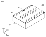
- FIG. 1 is a perspective view of a power conversion device 100
- FIG. 2 is an exploded perspective view of the power converter 100
- FIG. FIG. 3 is a cross-sectional view taken along IV-IV in FIG. 2
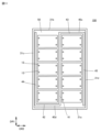
- FIG. 2 is a plan view of the power conversion device 100 in which illustration of a substrate 60 is omitted
- 4 is an enlarged cross-sectional view of a substrate 60
- FIG. 3A to 3C are process diagrams showing a method for manufacturing the power conversion device 100.
- FIG. FIG. 3 is a cross-sectional view of a power conversion device 100 according to Modification 1
- FIG. 11 is a perspective view of a power conversion device 100 according to Modification 2;
- FIG. 10 is a bottom view of a substrate 60 included in a power conversion device 100B according to Modification 1.
- FIG. 10 is an enlarged cross-sectional view of a power conversion device 100B according to Modification 1.
- FIG. 11 is an enlarged cross-sectional view of a power conversion device 100B according to Modification 2; It is a side view of the heat sink 40 which the power converter device 100C has. It is a top view of the board
- FIG. 11 is an example of a side view of a heat sink 40 included in a power conversion device 100D according to Modification 1.
- FIG. 10 is another example of a side view of the heat sink 40 included in the power conversion device 100D according to Modification 1.
- FIG. It is an example of a cross-sectional view of a power conversion device 100D according to Modification 2.
- FIG. 11 is another example of a cross-sectional view of a power conversion device 100D according to Modification 2.
- Embodiment 1 A power converter according to Embodiment 1 will be described.
- the power conversion device according to Embodiment 1 is referred to as power conversion device 100 .
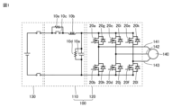
- FIG. 1 is a circuit diagram of the power converter 100.
- the power converter 100 has a peripheral circuit 110 and a switching circuit 120 .
- the peripheral circuit 110 has a plurality of circuit components 10.
- the plurality of circuit components 10 are a capacitor 10a, an inductor 10b, a contactor 10c, a discharging resistor 10d and a charging resistor 10e.
- Capacitor 10a, inductor 10b and contactor 10c are connected in series.
- Inductor 10b is arranged between capacitor 10a and contactor 10c.
- a discharging resistor 10d and a charging resistor 10e are connected in parallel to the capacitor 10a and the contactor 10c, respectively.
- Peripheral circuit 110 is connected to DC supply circuit 130 .
- the switching circuit 120 is, for example, a three-phase inverter circuit.
- the switching circuit 120 has multiple circuit components 20 .
- the plurality of circuit components 20 are transistors 20a-20f and diodes 20g-20l.
- the drain of the transistor 20a is electrically connected to one electrode of the capacitor 10a.
- the source of transistor 20a is electrically connected to the drain of transistor 20b.
- the source of transistor 20b is electrically connected to the other electrode of capacitor 10a.
- the anode of diode 20g is electrically connected to the source of transistor 20a.
- the cathode of diode 20g is electrically connected to the drain of transistor 20a.
- the anode of diode 20h is electrically connected to the source of transistor 20b.
- the cathode of diode 20h is electrically connected to the drain of transistor 20b.
- the transistor 20c, the transistor 20d, the diode 20i and the diode 20j are connected in the same manner as the transistor 20a, the transistor 20b, the diode 20g and the diode 20h, respectively.
- Transistor 20e, transistor 20f, diode 20k, and diode 20l are connected in the same manner as transistor 20a, transistor 20b, diode 20g, and diode 20h, respectively.
- the gates of transistors 20a-20f are connected to a control circuit.
- the switching circuit 120 is connected to the motor 140.
- Motor 140 is, for example, a three-phase motor.
- Motor 140 has input line 141 , input line 142 , and input line 143 .
- the input line 141 is electrically connected to the source of the transistor 20a and the drain of the transistor 20b.
- the input line 142 is electrically connected to the source of the transistor 20c and the drain of the transistor 20d.
- the input line 143 is electrically connected to the source of the transistor 20e and the drain of the transistor 20f.
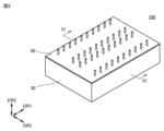
- FIG. 2 is a perspective view of the power converter 100.
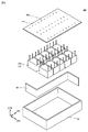
- FIG. FIG. 3 is an exploded perspective view of the power conversion device 100.
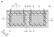
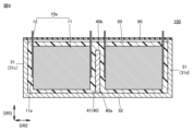
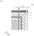
- FIG. FIG. 4 is a cross-sectional view along IV-IV in FIG.
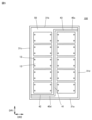
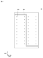
- FIG. 5 is a plan view of the power conversion device 100 with the substrate 60 omitted.
- FIG. 6 is an enlarged cross-sectional view of the substrate 60.
- the power converter 100 has a plurality of circuit components 10, a housing 30, a radiator plate 40, a heat transfer member 50, and a substrate 60.
- the housing 30 has side walls 31 and a bottom wall 32 .
- the side wall 31 has a first side wall portion 31a and a second side wall portion 31b, and a third side wall portion 31c and a fourth side wall portion 31d.
- the first side wall portion 31a and the second side wall portion 31b face each other with a gap therebetween in the first direction DR1.
- the third side wall portion 31c and the fourth side wall portion 31d face each other with a gap therebetween in the second direction DR2.
- the second direction DR2 is a direction orthogonal to the first direction DR1.
- the side wall 31 has, for example, a rectangular shape in plan view.
- the bottom wall 32 continues to the lower ends of the side walls 31 .
- the housing 30 is made of rigid material.
- the housing 30 is made of, for example, a metal material.
- the housing 30 is made of any metal material selected from the group consisting of copper (Cu), copper alloys, aluminum (Al), aluminum alloys, iron (Fe), and iron alloys.
- a specific example of the copper alloy is phosphor bronze, a specific example of the aluminum alloy is ADC12 specified in the JIS standard, and a specific example of the iron alloy is SUS304.
- the housing 30 may be made of a resin material.
- This resin material is, for example, one selected from the group consisting of polybutylene terephthalate (PBT), polyphenylene sulfide (PPS) and polyetheretherketone (PEEK).
- This resin material may contain a thermally conductive filler.
- Housing 30 is preferably made of a non-magnetic material.
- the housing 30 is formed by cutting, die casting or forging, for example.
- the housing 30 may be formed by sheet metal pressing and welding.
- the housing 30 may be formed by molding using a mold.
- the circuit component 10 is a capacitor 10a.
- the capacitor 10a is an element that stores or releases electric charge.
- Capacitor 10a is, for example, a film capacitor.
- the circuit component 10 has an element body and a conducting terminal. When the circuit component 10 is a capacitor 10 a , the element body is the capacitor element 11 and the conducting terminal is the conducting terminal 12 .
- Capacitor 10 a further has outer case 13 and resin 14 .
- the capacitor element 11 is configured, for example, by winding a metal film and a dielectric film placed on the metal film.
- a dielectric film is, for example, a plastic film.
- Plastic films are made of, for example, polyethylene terephthalate (PET), polyphenylene sulfide, polypropylene (PP), polyethylene naphthalate (PEN), polycarbonate (PC), polytetrafluoroethylene (PTFE), and the like.
- the plastic film is preferably made of polyethylene terephthalate from the viewpoint of manufacturing costs, and polypropylene is preferable from the viewpoint of high-frequency characteristics.
- the plastic film is preferably made of polyphenylene sulfide from the viewpoint of heat resistance and high frequency characteristics, and preferably made of polyethylene naphthalate from the viewpoint of size reduction and heat resistance. From the viewpoint of heat resistance, the plastic film is preferably made of polytetrafluoroethylene.
- the capacitance of the capacitor 10a is proportional to the dielectric constant and area of the dielectric film, and inversely proportional to the distance between the metal films. A charge accumulates in the dielectric film.
- Both end surfaces of the capacitor element 11 are electrode surfaces 11a to which the current-carrying terminals 12 are electrically connected.
- the electrode surface 11a may be formed by depositing metal on a plastic film.
- the current-carrying terminal 12 plays a role of allowing a current from the outside to flow through the capacitor element 11 .
- the conducting terminal 12 extends along the third direction DR3.
- the third direction DR3 is orthogonal to the first direction DR1 and the second direction DR2.
- the energizing terminal 12 is made of a conductive material.
- the conducting terminal 12 is made of, for example, copper, copper alloy, silver (Ag), silver alloy, gold (Au), gold alloy, tin (Sn), tin alloy, nickel (Ni) alloy, aluminum, titanium (Ti), molybdenum. (Mo).
- a plated layer of chromium (Cr), nickel, copper, tin, silver, zinc (Zn), gold, or the like is formed on the surface of the current-carrying terminal 12 from the viewpoint of improving corrosion resistance, heat resistance, and electrical conductivity. is preferred.
- the outer case 13 is made of an insulating material.
- the outer case 13 is made of, for example, a resin material.
- the outer case 13 is made of a resin material selected from the group consisting of polypropylene, polybutylene terephthalate, polyphenylene sulfide, and polyetheretherketone, for example.
- the capacitor element 11 and the current-carrying terminals 12 are housed inside the outer case 13 . However, a part of the conducting terminal 12 protrudes from the upper surface of the outer case 13 .
- the outer case 13 insulates the capacitor element 11 from the surroundings and prevents the invasion of the capacitor element 11 by substances such as air and moisture that change the electrostatic induction action.
- the resin 14 is electrically insulating.
- the resin 14 is preferably a heat resistant resin.
- Specific examples of resin 14 include epoxy or tape wrap resin.
- the resin 14 is filled inside the outer case 13 . As a result, the capacitor element 11 and the conducting terminals 12 are sealed, and the capacitor element 11 is insulated from the outside.
- the bottom surface of capacitor 10 a (the bottom surface of outer case 13 ) may or may not be in contact with bottom wall 32 .
- the plurality of capacitors 10a are housed inside the housing 30.
- a plurality of capacitors 10a are arranged in two rows (first row and second row, respectively) along the first direction DR1.
- the electrode surfaces 11a of the capacitors 10a belonging to the first row face the electrode surfaces 11a of the capacitors 10a belonging to the second row.
- the radiator plate 40 is housed inside the housing 30 .
- the heat sink 40 has a lower end 40a and an upper end 40b.
- the lower end 40a and the upper end 40b are ends of the heat sink 40 in the third direction DR3.
- the lower end 40 a is in contact with the bottom wall 32 .
- the upper end 40b is the opposite end of the lower end 40a.
- the radiator plate 40 has a side surface 40c and a side surface 40d.
- the side surface 40c and the side surface 40d are end surfaces of the heat sink 40 in the thickness direction.
- the side surface 40d is the opposite surface of the side surface 40c.
- the arithmetic average roughness of the side surface 40c and the arithmetic average roughness of the side surface 40d are preferably 6.3 ⁇ m or more.
- the heat sink 40 has a first portion 41, a second portion 42, and a third portion 43 in plan view.
- the first portion 41 extends along the first direction DR1.
- the first portion 41 is arranged between the first row of capacitors 10a and the second row of capacitors 10a. That is, the electrode surfaces 11a of the capacitors 10a forming the first row face the side surfaces 40c on the first portion 41, and the electrode surfaces 11a of the capacitors 10a forming the second row are on the first portion 41. It faces the side surface 40d.
- the side surface of the outer case 13 may be in contact with the first portion 41 or may not be in contact with the first portion 41 .
- the electrode surface 11a on the first portion 41 side of the capacitor 10a belonging to the first row (second row) and the side surface 40c (side surface 40d) of the first portion 41 are preferably substantially parallel.
- the electrode surface 11a on the side opposite to the first portion 41 of the capacitor 10a belonging to the first row (second row) and the inner wall surface of the third side wall portion 31c (fourth side wall portion 31d) are substantially parallel. preferably. It is preferable that the bottom surface of the capacitor 10a and the inner wall surface of the bottom wall 32 are substantially parallel. Note that two surfaces being substantially parallel means that the angle formed by the two surfaces is within a range of ⁇ 5° or less.
- the second portion 42 extends from one end of the first portion 41 in the first direction DR1 toward the third side wall portion 31c along the second direction DR2.
- the third portion 43 extends from the other end of the first portion 41 in the first direction DR1 toward the fourth side wall portion 31d along the second direction DR2.
- the heat sink 40 is bent at the connecting portion between the first portion 41 and the second portion 42 and the connecting portion between the first portion 41 and the third portion 43 . From another point of view, the connecting portion between the first portion 41 and the second portion 42 and the connecting portion between the first portion 41 and the third portion 43 are bent portions of the heat sink 40 .
- a side surface 40d of the second portion 42 faces the side wall 31 (first side wall portion 31a).
- a side surface 40c in the third portion 43 faces the side wall 31 (second side wall portion 31b).
- the radiator plate 40 may be made of the same material as the housing 30 or may be made of a material different from that of the housing 30 .
- the radiator plate 40 is formed by cutting, die casting, or forging, for example.
- the heat sink 40 may be formed by sheet metal pressing and welding.
- the radiator plate 40 may be formed by molding using a mold.
- the width of the heat sink 40 in the second direction DR2 is, for example, greater than the width of the heat sink 40 in the first direction DR1. Most preferably, the width of the heat sink 40 in the second direction DR2 is equal to the distance in the second direction DR2 between the third side wall portion 31c and the fourth side wall portion 31d. A value obtained by subtracting the width of the heat sink 40 in the second direction DR2 from the distance in the second direction DR2 between the third side wall portion 31c and the fourth side wall portion 31d may be smaller than 0.5 mm.
- the heat transfer member 50 is a potting material made of an electrically insulating material.
- the heat transfer member 50 is made of, for example, a resin material.
- This resin material is, for example, silicone, urethane, epoxy, or the like. This resin material may contain a thermally conductive filler.
- the heat transfer member 50 preferably has curability or adhesiveness.
- the heat transfer member 50 preferably has water resistance.
- the heat transfer member 50 is arranged inside the housing 30 . Thereby, the plurality of capacitors 10a and the heat sink 40 are sealed inside the housing 30, and the capacitors 10a and the heat sink 40 are thermally connected.
- the heat transfer member 50 is preferably arranged so that the outer case 13 is embedded in the heat transfer member 50 . However, the conducting terminal 12 protrudes from the heat transfer member 50 .
- the heat transfer member 50 and the substrate 60 are not in contact with each other, and there is a gap between the heat transfer member 50 and the substrate 60 .
- the upper end 40 b is below the upper surface of the heat transfer member 50 . That is, the radiator plate 40 is embedded in the heat transfer member 50 .
- the board 60 is, for example, a printed board. It has a plurality of base materials 61 and a plurality of wiring members 62 .
- the base material 61 and the wiring member 62 are alternately laminated in the thickness direction of the substrate 60 .
- the base material 61 is made of an electrically insulating material.
- the base material 61 is made of, for example, epoxy containing glass-reinforced fiber, phenolic resin, polyphenylene sulfide, polyetheretherketone, or the like.
- the wiring member 62 is made of a conductive material, that is, a material with low electrical resistivity and high thermal conductivity.
- the wiring member 62 is made of, for example, copper, copper alloy, silver, silver alloy, gold, gold alloy, tin, tin alloy, nickel alloy, or the like.
- the thickness of the wiring member 62 is, for example, 1 ⁇ m or more and 5000 ⁇ m or less.
- a through hole 60 a is formed in the substrate 60 .
- a conductor layer 63 is formed on the inner wall surface of the through hole 60a.
- the energizing terminal 12 is electrically connected to the wiring member 62 by passing the energizing terminal 12 through the through-hole 60 a and placing the joining member 64 (not shown) between the conductor layer 63 and the energizing terminal 12 . It is connected.
- the joining member 64 is, for example, a solder alloy.
- the conducting terminals 12 may be connected to the wiring members 62 on the surface of the substrate 60 .
- Electronic components forming a control circuit are arranged on the substrate 60 .
- the substrate 60 may be a ceramic substrate or a metal substrate.
- Substrate 60 is preferably in contact with sidewall 31 .
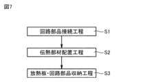
- FIG. 7 is a process diagram showing a method of manufacturing the power conversion device 100.
- the power conversion device 100 includes a circuit component connection step S1, a heat transfer member arrangement step S2, and a radiator plate/circuit component accommodation step S3.
- the capacitor 10a and the substrate 60 are electrically connected. Electrical connection between the capacitor 10a and the substrate 60 is made by soldering, for example.
- the heat transfer member placement step S2 is performed after the circuit component connection step S1. In the heat transfer member placement step S ⁇ b>2 , the heat transfer member 50 is placed inside the housing 30 .
- the heat sink/circuit component housing step S3 is performed after the heat transfer member placement step S2.
- the heat sink 40 is housed in the housing 30 .
- the plurality of capacitors 10a are also accommodated in the housing 30. As shown in FIG. Thereby, the capacitor 10 a and the heat sink 40 are thermally connected by the heat transfer member 50 .
- a plurality of capacitors 10a are densely arranged. As the distance between the adjacent capacitors 10a becomes shorter, the heat generation of the adjacent capacitors 10a interferes, and the temperature rise of the capacitors 10a increases. An excessive rise in the temperature of the capacitor 10a causes characteristic deterioration, destruction, and shortening of the life of the capacitor 10a.
- the capacitor 10 a and the heat sink 40 are thermally connected by the heat transfer member 50 . Therefore, the heat generated in the capacitor 10 a is transmitted to the housing 30 via the heat transfer member 50 and the heat sink 40 and radiated from the bottom wall 32 . Thus, according to the power conversion device 100, it is possible to suppress the temperature rise of the capacitor 10a.
- the heat sink 40 (first portion 41) is arranged to face the electrode surface 11a of the capacitor 10a belonging to the first row and the electrode surface 11a of the capacitor 10a belonging to the second row. Therefore, the electrode surface 11a, which generates a large amount of heat, can be efficiently cooled, and the temperature rise of the capacitor 10a can be further suppressed.
- the electrode surface 11a on the side opposite to the first portion 41 of the capacitor 10a belonging to the first row faces the side wall 31 (third side wall portion 31c) with the heat transfer member 50 interposed therebetween.
- the electrode surface 11a on the side opposite to the first portion 41 of the capacitor 10a belonging to the second row faces the side wall 31 (fourth side wall portion 31d) with the heat transfer member 50 interposed therebetween. Therefore, the heat generated on the electrode surface 11a can be radiated also from the side wall 31, and the temperature rise of the capacitor 10a can be further suppressed.
- Heat from the capacitor 10a on surfaces other than the electrode surface 11a is also transferred to the side wall 31 or the heat sink 40 via the heat transfer member 50, so that the temperature rise of the capacitor 10a can be suppressed.
- radiator plate 40 has first portion 41 extending along first direction DR1. Both the capacitors 10a arranged at the ends other than both ends in the first direction DR1 and the capacitors 10a arranged at both ends in the first direction DR1 are arranged to face the first portion 41 with the heat transfer member 50 interposed therebetween. , the temperature is equalized between the capacitors 10a arranged at the ends other than the ends in the first direction DR1 and the capacitors 10a arranged at the ends in the first direction DR1.
- the required heat resistance of the capacitor 10a is determined based on the capacitor 10a whose temperature rises the most. Therefore, according to the power conversion device 100, a capacitor with low heat resistance can be used as the capacitor 10a.
- the electrode surface 11a of the capacitor 10a belonging to the first row and the electrode surface 11a of the capacitor 10a belonging to the second row are opposed to each other, and the heat sink 40 (first portion 41) Since it is arranged between the capacitors 10a belonging to the first row and the capacitors 10a belonging to the second row, a plurality of heat sinks 40 are not required, and the manufacturing cost of the power converter 100 can be reduced. can.
- the radiator plate 40 has a second portion 42 and a third portion 43 .
- a side surface 40d on the second portion 42 and a side surface 40c on the third portion 43 face the first side wall portion 31a and the second side wall portion 31b, respectively. Therefore, in the power conversion device 100, the heat of the radiator plate 40 is transmitted to the side wall 31, and the heat is easily radiated from the side wall 31, so that the temperature rise of the capacitor 10a can be further suppressed.
- the heat sink 40 since the bottom wall 32 and the heat sink 40 are in contact with each other, heat is easily transferred from the heat sink 40 to the bottom wall 32, and the temperature rise of the capacitor 10a can be further suppressed. Since the heat sink 40 has the second portion 42 and the third portion 43, the contact area between the heat sink 40 and the bottom wall 32 is increased. The contact thermal resistance between the heat sink 40 and the bottom wall 32 decreases as the contact area between the heat sink 40 and the bottom wall 32 increases. Therefore, in the power conversion device 100, the heat of the radiator plate 40 is transmitted to the bottom wall 32, and the heat is easily radiated from the bottom wall 32, so that the temperature rise of the capacitor 10a can be further suppressed.
- the heat sink 40 since the heat sink 40 is bent to have the second portion 42 and the third portion 43 , the heat sink 40 can stand on the bottom wall 32 by itself. A jig for supporting the heat radiating plate 40 is not required when it is housed, and the manufacturing cost of the power conversion device 100 can be reduced.
- the width of the heat sink 40 in the second direction DR2 is equal to the distance in the second direction DR2 between the third side wall portion 31c and the fourth side wall portion 31d or between the third side wall portion 31c and the fourth side wall portion 31d , the distance in the second direction DR2 from the width of the heat sink 40 in the second direction DR2 is smaller than 0.5 mm, the second portion 42 and the third portion 43 allow the heat sink 40 to move in the housing 30. can be positioned. By positioning the heat sink 40, the positioning of the capacitor 10a is facilitated, and the assemblability of the power conversion device 100 is improved.
- the arithmetic roughness of the side surface 40c and the arithmetic average roughness of the side surface 40d are 6.3 ⁇ m or more, the contact area between the heat sink 40 and the heat transfer member 50 increases, and the heat sink 40 and the heat transfer member increase. 50, the temperature rise of the capacitor 10a can be further suppressed.
- the capacitor 10a is sealed with the heat transfer member 50, the position of the capacitor 10a can be fixed, and the capacitor 10a can be protected, dust-proofed, and insulated. Further, when the heat transfer member 50 is arranged inside the housing 30 so that the outer case 13 is buried in the heat transfer member 50, the vibration resistance of the power converter 100 is improved. In this case, the contact area between the capacitor 10a and the heat transfer member 50 increases, and the contact thermal resistance between the capacitor 10a and the heat transfer member 50 decreases, so that the temperature rise of the capacitor 10a can be further suppressed. can.
- the heat of the capacitor 10a is radiated to the heat transfer member 50, but if the substrate 60 is inside the heat transfer member 50 (sealed in the heat transfer member 50), the linear expansion of the heat transfer member 50 will occur. Due to the difference between the coefficient of linear expansion of the substrate 60 and the coefficient of linear expansion of the substrate 60 , stress is applied to the substrate 60 and the energizing terminals 12 due to temperature changes, and the energizing terminals 12 may be damaged or soldered to connect the energizing terminals 12 and the substrate 60 . It causes cracks in the part.
- the substrate 60 is inside the heat transfer member 50, it becomes difficult to connect other devices to the power conversion device 100. That is, the connecting portion mounted on the substrate 60 for connection with another device is arranged so as to be exposed from the heat transfer member 50, or the other substrate connected to the substrate 60 is arranged outside the heat transfer member 50. There is a need to. As a result, the parts used in the power conversion device 100 and the assembly process of the power conversion device 100 are restricted. If there is a gap between the heat transfer member 50 and the substrate 60 (the substrate 60 is not sealed with the heat transfer member 50), such restrictions can be avoided.
- the heat transfer members 50 are unevenly distributed within the housing 30, the area where the heat transfer members 50 are scarce will be thermally connected to the housing 30, which may increase the temperature of the capacitor 10a. If the upper end 40b is lower than the upper end of the heat transfer member 50, even if the adjacent capacitors 10a are partitioned by the radiator plate 40, the heat transfer member 50 before curing will not move in the heat transfer member placement step S2. Therefore, the liquid level of the heat transfer member 50 before hardening is easily uniformized, the heat transfer member 50 is evenly filled in the housing 30, and the temperature of the capacitor 10a is uniformed.
- the electrode surface 11a on the first portion 41 side of the capacitor 10a belonging to the first row (second row) and the side surface 40c (side surface 40d) on the first portion 41 are substantially parallel, the electrode The thermal resistance between the surface 11a and the heat sink 40 can be made uniform. Further, in this case, since the capacitor 10a is less likely to come into contact with the housing 30 and the heat sink 40 during assembly, damage to the capacitor 10a can be suppressed.
- the substrate 60 and the side wall 31 are in contact with each other, the heat generated in the capacitor 10 a and transmitted to the substrate 60 is transmitted to the side wall 31 and is easily radiated from the side wall 31 . Therefore, in this case, it is possible to further suppress the temperature rise of the capacitor 10a.
- the electrode surface 11a on the side opposite to the first portion 41 of the capacitor 10a belonging to the first row (second row) and the inner wall surface of the third side wall portion 31c (fourth side wall portion 31d) are substantially parallel.
- the thermal resistance between the electrode surface 11a and the sidewall 31 can be made uniform.
- the thermal resistance between the capacitor 10a and the bottom wall 32 can be made uniform.
- the radiator plate 40 is arranged between the adjacent capacitors 10a, so the radiator plate 40 functions as an electromagnetic shield between the adjacent capacitors 10a.
- the radiator plate 40 since the radiator plate 40 is arranged between the adjacent capacitors 10a, it also functions as a firewall when the capacitor 10a fails and explodes.
- FIG. 8 is a cross-sectional view of a power conversion device 100 according to Modification 1. As shown in FIG. FIG. 8 shows a cross section at a position corresponding to IV-IV in FIG. As shown in FIG. 8, capacitor 10a may not have outer case 13 and resin . Even if the capacitor 10 a does not have the outer case 13 and the resin 14 , the heat transfer member 50 can insulate the capacitor element 11 .
- the heat transfer resistance between the capacitor 10a and the heat sink 40 is reduced, so that the temperature rise of the capacitor 10a can be further suppressed. can be done.
- the size of the capacitor 10a can be reduced, so that the power conversion device 100 can be reduced in size.
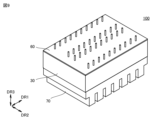
- FIG. 9 is a perspective view of a power conversion device 100 according to Modification 2.
- power converter 100 may further include a cooler.
- This cooler is, for example, a heat sink 70 .
- a heat sink 70 is attached to the outside of the housing 30 . More specifically, heat sink 70 is attached to bottom wall 32 .
- the heat sink 70 may be cooled by passing a coolant such as water or air through it.
- the heat sink 70 is made of a material with high thermal conductivity.
- the heat sink 70 is made of copper, aluminum, iron, or the like, for example.
- the shape of the fin portion of the heat sink 70 is, for example, plate-like or conical shape.
- the fin portion of the heat sink 70 extends, for example, in the third direction DR3.
- the plate-shaped fin portions of the heat sink 70 may be arranged along the first direction DR1 as shown in FIG. 9, or may be arranged along the second direction DR2.
- the thickness, number, and length of the fins of the heat sink 70 may be appropriately changed according to the coolant (water, air, etc.) and cooling method.
- the number of capacitors 10a increases when the power conversion device 100 is further increased in output.
- the capacitors 10a are arranged in three or more rows, the number of capacitors 10a adjacent in the first direction DR1 and the number of capacitors 10a adjacent in the second direction DR2 increase, so the temperature rise of the capacitors 10a increases.
- the heat sink 70 needs to promote cooling.
- the heat sink 70 is arranged on the outer wall surface of the bottom wall 32 .
- FIG. 10 is a perspective view of a power conversion device 100 according to Modification 3.
- the power conversion device 100 may have screws 80 .
- Screw 80 is, for example, a countersunk screw or a pan screw.
- the screw 80 is passed through a through hole 60 b (not shown in FIG. 10 ) formed in the substrate 60 and screwed into a threaded hole formed in the side wall 31 .
- the substrate 60 is thereby fixed to the side wall 31 .
- Screws 80 may be rivets.
- the method of fixing the substrate 60 to the side wall 31 is not limited to screwing.
- Substrate 60 may be secured to side wall 31 by gluing, crimping, welding, or the like.
- the electrode surface 11a on the side of the first portion 41 of the capacitor 10a belonging to the first row (second row) and the side surface 40c on the first portion 41 are separated. (Side surface 40d) is prevented from being substantially parallel. As a result, the thermal resistance between the electrode surface 11a and the heat sink 40 can be made uniform.
- the thermal resistance between the electrode surface 11a and the side wall 31 and the thermal resistance between the capacitor 10a and the bottom wall 32 can be made uniform.
- the capacitor 10a is also positioned within the housing 30, so the assembling efficiency of the power converter 100 is improved.
- FIG. 11 is a plan view of a power conversion device 100 according to Modification 4 in which illustration of the substrate 60 is omitted. As shown in FIG. 11 , the heat sink 40 may further have a fourth portion 44 and a fifth portion 45 .
- the fourth portion 44 and the fifth portion 45 extend along the first direction DR1.
- the fourth portion 44 is connected to the end of the second portion 42 opposite to the first portion 41 .
- the fifth portion 45 is connected to the end of the third portion 43 opposite to the first portion 41 . From another point of view, the fourth portion 44 faces the electrode surface 11a on the side opposite to the first portion 41 of the capacitor 10a belonging to the first row, and the fifth portion 45 faces the second row. facing the electrode surface 11a opposite the first portion 41 of the capacitor 10a belonging to the .
- the heat generated on the electrode surface 11a of the capacitor 10a opposite to the first portion 41 is also easily radiated to the radiator plate 40.
- the heat generated in the electrode surface 11a on the opposite side of the first portion 41 can be uniformly heated by the heat sink 40 and then radiated from the side wall 31, thereby improving the heat radiation performance.
- the rise can be further suppressed.
- the contact area between the heat sink 40 and the bottom wall 32 is further increased, so that the contact thermal resistance between the heat sink 40 and the bottom wall 32 can be further reduced, and the capacitor 10a temperature rise can be further suppressed.
- Embodiment 2 A power converter according to Embodiment 2 will be described.
- the power conversion device according to Embodiment 2 is referred to as a power conversion device 100A.
- points different from the power conversion device 100 will be mainly described, and redundant description will not be repeated.
- the power conversion device 100A has a plurality of circuit components 10 (capacitors 10a), a housing 30, a heat transfer member 50, and a substrate 60. Regarding this point, the configuration of the power conversion device 100A is common to the configuration of the power conversion device 100 .
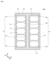
- FIG. 12 is a plan view of the power converter 100A with the substrate 60 omitted. As shown in FIG. 12 , the power converter 100A has a heat sink 91 and a heat sink 92 instead of the heat sink 40 . In this regard, the configuration of the power conversion device 100A is different from the configuration of the power conversion device 100. FIG.
- the radiator plate 91 and the radiator plate 92 are adjacent to each other in the second direction DR2.
- the heat sink 91 has a first portion 91a, a second portion 91b, and a third portion 91c.
- the heat sink 92 has a first portion 92a, a second portion 92b, and a third portion 92c.
- the first portion 91a extends along the first direction DR1.
- the second portion 91b and the third portion 91c each extend from both ends of the first portion 91a toward the third side wall portion 31c along the second direction DR2.
- the first portion 92a extends along the first direction DR1.
- the second portion 92b and the third portion 92c each extend from both ends of the first portion 92a toward the fourth side wall portion 31d along the second direction DR2.
- the first portion 91a and the first portion 92a are arranged between the capacitors 10a belonging to the first row and the capacitors 10a belonging to the second row.
- the electrode surface 11a on the side of the first portion 91a of the capacitor 10a belonging to the first row faces the first portion 91a.
- the electrode surface 11a on the side of the first portion 92a of the capacitor 10a belonging to the second row faces the first portion 92a.
- the sum of the width of the heat sink 91 in the second direction DR2 and the width of the heat sink 92 in the second direction DR2 is equal to the distance in the second direction DR2 between the third side wall portion 31c and the fourth side wall portion 31d. Most preferred. A value obtained by subtracting the sum of the width of the heat sink 91 in the second direction DR2 and the width of the heat sink 92 in the second direction DR2 from the distance in the second direction DR2 between the third side wall portion 31c and the fourth side wall portion 31d is , may be less than 0.5 mm.
- both the heat generated in the capacitors 10a belonging to the first row and the heat generated in the capacitors 10a belonging to the second row are transmitted to the radiator plate 40 via the heat transfer member 50. Temperature rises easily.
- the power conversion device 100A the heat generated in the capacitors 10a belonging to the first row is transmitted to the radiator plate 91, but the heat generated in the capacitors 10a belonging to the second row is transmitted to the radiator plate 92. Therefore, according to the power conversion device 100A, it is possible to further suppress the temperature rise of the capacitors 10a and further equalize the temperature among the plurality of capacitors 10a.
- the sum of the width of the heat sink 91 in the second direction DR2 and the width of the heat sink 92 in the second direction DR2 is equal to the distance in the second direction DR2 between the third side wall portion 31c and the fourth side wall portion 31d;
- a value obtained by subtracting the sum of the width of the heat sink 91 in the second direction DR2 and the width of the heat sink 92 in the second direction DR2 from the distance in the second direction DR2 between the third side wall portion 31c and the fourth side wall portion 31d is 0. If it is smaller than 0.5 mm, the heat sink 91 and the heat sink 92 can be positioned within the housing 30 . By positioning the radiator plate 91 and the radiator plate 92, the positioning of the capacitor 10a is facilitated, and the assembling property of the power converter 100A is improved.
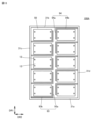
- FIG. 13 is a plan view of a power conversion device 100A according to Modification 1 in which illustration of the substrate 60 is omitted. As shown in FIG. 13 , the power converter 100A may have a plurality of heat sinks 93 and 94 instead of the heat sinks 91 and 92 .
- the radiator plate 93 is L-shaped in plan view.
- the heat sink 93 has a first portion 93a and a second portion 93b.
- the first portion 93a extends along the first direction DR1.
- the second portion 93b extends from one end of the first portion 93a in the first direction DR1 toward the third side wall portion 31c along the second direction DR2.
- the first portion 93a is arranged between two capacitors 10a adjacent in the second direction DR2.
- the second portion 93b belongs to the first row and is arranged between two capacitors 10a adjacent in the first direction DR1.
- the second portion 93b of the heat sink 93 closest to the first side wall portion 31a belongs to the first row, and the capacitor 10a closest to the first side wall portion 31a is connected to the first side wall portion 31a. is placed between.
- the radiator plate 94 is L-shaped in plan view.
- the heat sink 94 has a first portion 94a and a second portion 94b.
- the first portion 94a extends along the first direction DR1.
- the second portion 94b extends from the other end of the first portion 94a in the first direction DR1 toward the fourth side wall portion 31d along the second direction DR2.
- the heat sink 94 preferably has the same shape as the heat sink 93 .
- the first portion 94a is arranged between two capacitors 10a adjacent in the second direction DR2.
- the first portion 94a is closer to the capacitors 10a belonging to the second row than the first portion 93a.
- the second portion 94b belongs to the second row and is arranged between two capacitors 10a adjacent in the first direction DR1.
- the second portion 94b of the radiator plate 94 closest to the second side wall portion 31b belongs to the second row, and the capacitor 10a closest to the second side wall portion 31b is connected to the second side wall portion 31b. is placed between.
- one heat sink 93 or one heat sink 94 is arranged for one capacitor 10a.
- the heat transfer area from the capacitor 10a to the heat sink increases, and the thermal resistance between the capacitor 10a and the heat sink decreases, thereby further suppressing the temperature rise of the capacitor 10a.
- the heat sink 93 and the heat sink 94 have a simple shape, they are easy to process. If the heat sink 93 and the heat sink 94 have the same shape, the productivity is particularly improved.
- at least one of the radiator plate 93 and the radiator plate 94 is provided between the two adjacent capacitors 10a, the function as a fire wall is further improved in the event that the capacitor 10a fails and explodes. .
- FIG. 14 is a plan view of a power conversion device 100A according to Modification 2 in which illustration of the substrate 60 is omitted.
- the power converter 100A may have a plurality of heat sinks 95 instead of the heat sinks 91 and 92 . It is preferable that the plurality of heat sinks 95 have the same shape.
- the heat sink 95 has a first portion 95a, a second portion 95b, and a third portion 95c.
- the first portion 95a extends along the first direction DR1 between two capacitors 10a that are adjacent in the second direction DR2.
- the second portion 95b extends from one end of the first portion 95a in the first direction DR1 toward the third side wall portion 31c along the second direction DR2.
- the third portion 95c extends from the other end of the first portion 95a in the first direction DR1 toward the fourth side wall portion 31d along the second direction DR2.
- the second portion 95b belongs to the first row and is arranged between two capacitors 10a adjacent in the first direction DR1.
- the second portion 95b of the radiator plate 95 closest to the first side wall portion 31a belongs to the first row, and is connected to the capacitor 10a closest to the first side wall portion 31a and the first side wall portion 31a. is placed between.
- the third portion 95c belongs to the second row and is arranged between two capacitors 10a adjacent in the first direction DR1.
- the third portion 95c of the radiator plate 95 closest to the second side wall portion 31b belongs to the second row, and is located between the capacitor 10a closest to the second side wall portion 31b and the second side wall portion 31b. is placed between.
- the heat transfer area from the capacitor 10a to the heat sink increases, and the heat transfer area between the capacitor 10a and the heat sink increases. Since the thermal resistance between the capacitors 10a is reduced, the temperature rise of the capacitor 10a is further suppressed. In addition, productivity is improved when a plurality of radiator plates 95 have the same shape. Furthermore, since the radiator plate 95 is provided between two adjacent capacitors 10a, the function as a fire wall is further improved in the event that the capacitor 10a fails and explodes.
- Embodiment 3 A power converter according to Embodiment 3 will be described.
- the power conversion device according to Embodiment 3 is referred to as a power conversion device 100B.
- points different from the power conversion device 100 will be mainly described, and redundant description will not be repeated.
- the power converter 100A has a plurality of circuit components 10 (capacitors 10a), a housing 30, a heat transfer member 50, a substrate 60, and screws 80. Regarding this point, the configuration of the power conversion device 100B is common to the configuration of the power conversion device 100 .
- FIG. 15 is a plan view of the substrate 60 included in the power conversion device 100B.
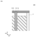
- FIG. 16 is an enlarged cross-sectional view of the power conversion device 100B.
- FIG. 16 shows an enlarged cross section at a position corresponding to IV-IV in FIG.
- the wiring member 62 has a first wiring member 62a and a second wiring member 62b.
- substrate 60 has conductor layer 65 . Regarding these points, the configuration of the power conversion device 100B is different from the configuration of the power conversion device 100 .
- the first wiring member 62 a is connected to the conductor layer 63 . Therefore, the first wiring member 62 a is electrically connected to the conducting terminal 12 by the conductor layer 63 and the joining member 64 .
- the first wiring member 62 a is exposed on the surface of the substrate 60 .
- the second wiring member 62b is electrically insulated from the first wiring member 62a. Therefore, the second wiring member 62b is electrically insulated from the conducting terminal 12.
- the conductor layer 65 is arranged on the inner wall surface of the through hole 60b.
- the second wiring member 62 b is connected to the conductor layer 65 . Screw 80 contacts conductor layer 65 .
- the heat generated in the capacitor 10a is transmitted to the first wiring member 62a via the conducting terminal 12, the conductor layer 63 and the joining member 64. Since the first wiring member 62a and the second wiring member 62b are thermally connected, the heat is further transmitted to the side wall 31 via the second wiring member 62b, the conductor layer 65 and the screw 80. As described above, in the power conversion device 100B, the heat generated in the capacitor 10a is transmitted to the housing 30 through the substrate 60, and the thermal resistance of the heat transfer path is reduced, so that the temperature rise of the capacitor 10a can be further suppressed. . In addition, since the substrate 60 has the conductor layers 63 and 65, the strength of the substrate 60 is increased, and warping of the substrate 60 is suppressed.
- FIG. 17 is a bottom view of a substrate 60 included in a power conversion device 100B according to Modification 1.
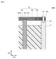
- FIG. FIG. 18 is an enlarged cross-sectional view of a power conversion device 100B according to Modification 1.
- FIG. 18 shows an enlarged cross section near the second portion 42 orthogonal to the second direction DR2.
- a groove 60c may be formed in the surface of the substrate 60 facing the heat sink 40.
- the heat sink 40 (upper end 40b) may be in contact with the bottom surface of the groove 60c. That is, the heat sink 40 is thermally connected to the substrate 60 .
- the heat sink 40 and the substrate 60 are thermally connected, the heat dissipation performance from the heat sink 40 to the substrate 60 and the heat dissipation performance from the substrate 60 to the heat sink 40 are improved, and the temperature of the capacitor 10a rises. is further suppressed.
- the radiator plate 40 is preferably fitted in the groove 60c. In this case, since the radiator plate 40 and the substrate 60 are strongly fixed, the vibration resistance of the power conversion device 100B is improved.
- FIG. 19 is an enlarged cross-sectional view of a power conversion device 100B according to Modification 2. As shown in FIG. FIG. 19 shows an enlarged cross section near the second portion 42 orthogonal to the second direction DR2. As shown in FIG. 19, the wiring member 62 may further have a third wiring member 62c. The third wiring member 62c is exposed from the bottom surface of the groove 60c. The third wiring member 62c is in contact with the radiator plate 40 (upper end 40b). The third wiring member 62c is electrically insulated from the first wiring member 62a. Since the third wiring member 62c overlaps the first wiring member 62a in plan view, it is thermally connected to the first wiring member 62a.
- the heat of the capacitor 10a is transferred to the third wiring member 62c through the radiator plate 40, and the heat is transferred to the first wiring member 62a.
- This heat is further transmitted to the side wall 31 (housing 30) via the second wiring member 62b, the conductor layer 65 and the screw 80.
- the heat transmitted from the capacitor 10a to the side wall 31 via the heat transfer member 50 is transmitted to the heat sink 40 via the screw 80, the conductor layer 65, the second wiring member 62b, and the third wiring member 62c. . Therefore, in this case, it is possible to further suppress the temperature rise of the capacitor 10a.
- Embodiment 4 A power converter according to Embodiment 4 will be described.
- the power conversion device according to Embodiment 4 is referred to as a power conversion device 100C.
- points different from the power conversion device 100 will be mainly described, and redundant description will not be repeated.
- the power conversion device 100C has a plurality of circuit components 10 (capacitors 10a), a housing 30, a heat transfer member 50, and a substrate 60. Regarding this point, the configuration of the power conversion device 100C is common to the configuration of the power conversion device 100 .
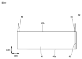
- FIG. 20 is a side view of the radiator plate 40 of the power converter 100C.
- the radiator plate 40 has projections 46 .
- the protrusion 46 protrudes from the upper end 40b along the third direction DR3.
- the position of the projection 46 on the upper end 40b is arbitrary.
- the number of protrusions 46 is preferably plural. It is preferable that the number of projections 46 is large.
- the protrusions 46 may be integrally formed with the heat sink 40, or may be attached to the heat sink 40 by soldering, welding, crimping, or the like.
- the protrusions 46 may be made of the same material as the heat sink 40, or may be made of a different material.
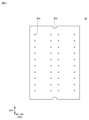
- FIG. 21 is a plan view of the substrate 60 included in the power conversion device 100C.
- the substrate 60 is formed with a through hole 60d.
- 60 d of through-holes may be arrange
- the through hole 60d may be a notch.
- the number of through holes 60 d is equal to the number of projections 46 .
- the protrusion 46 protrudes from the substrate 60 through the through hole 60 d when the substrate 60 is placed on the housing 30 . It is preferable that the protrusion 46 is long so that the amount of protrusion from the substrate 60 is increased. Regarding these points, the configuration of the power conversion device 100C is different from the configuration of the power conversion device 100 .
- the radiator plate 40 has the protrusions 46 and the substrate 60 has the through holes 60d, so that the substrate 60 can be easily positioned with respect to the radiator plate 40. Further, since the substrate 60 can be positioned with respect to the heat sink 40, the distance between the heat sink 40 and the capacitor 10a or the distance between the capacitor 10a and the side wall 31 is less likely to fluctuate. Thermalization becomes possible. Furthermore, the heat generated in the capacitor 10a and transmitted to the heat sink 40 is further transmitted to the protrusion 46, and the heat is radiated from the protrusion 46, so that the temperature rise of the capacitor 10a can be further suppressed.
- Embodiment 5 A power converter according to Embodiment 5 will be described.
- the power conversion device according to Embodiment 5 is referred to as a power conversion device 100D.
- points different from the power conversion device 100 will be mainly described, and redundant description will not be repeated.
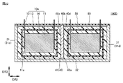
- FIG. 22 is a cross-sectional view of the power conversion device 100D.
- heat sink 40 may be connected to substrate 60 at upper end 40b. This connection is made by, for example, screwing, bonding, crimping, welding, or the like.
- the heat dissipation plate 40 is connected to the substrate 60, so the heat dissipation paths of the capacitor 10a are increased. That is, in the power conversion device 100D, the heat of the capacitor 10a is radiated from the bottom wall 32 from the electrode surface 11a via the heat transfer member 50 and the radiator plate 40, and is radiated from the side wall 31 from the conducting terminal 12 via the substrate 60. , heat is radiated from the bottom wall 32 from the energizing terminal 12 via the heat sink 40 and the substrate 60 . Further, in the power conversion device 100D, the heat sink 40 is connected to the substrate 60, and the substrate 60 is supported by the heat sink 40. Therefore, the bending of the substrate 60 due to the weight of the capacitor 10a is suppressed.
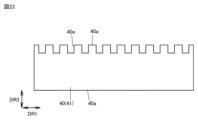
- FIG. 23 is an example of a side view of a heat sink 40 included in a power conversion device 100D according to Modification 1.
- a plurality of grooves 40e may be formed in upper end 40b.
- the bottom of the groove 40 e is below the upper surface of the heat transfer member 50 . That is, the heat sink 40 is embedded in the heat transfer member 50 at the portion where the groove 40e is formed. If the heat sink 40 is connected to the substrate 60, the heat transfer member 50 is biased in the housing 30, which may increase the temperature of the capacitor 10a.
- the heat transfer member 50 before curing will not pass through the groove 40e in the heat transfer member placement step S2.
- the heat transfer member 50 in the housing 30 is evenly filled, and the temperature of the capacitor 10a is equalized.
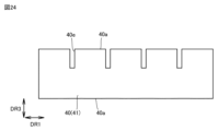
- FIG. 24 is another example of a side view of the heat sink 40 included in the power converter 100D according to Modification 1.
- the heat of the capacitor 10a is radiated from the housing 30 via the radiator plate 40, so the groove 40e is preferably formed at a position not facing the electrode surface 11a. Also, if the groove 40e is too deep, the heat conduction along the longitudinal direction of the heat sink 40 becomes small. Preferably.
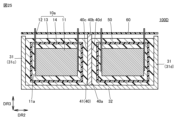
- FIG. 25 is an example of a cross-sectional view of a power conversion device 100D according to Modification 2.
- FIG. 26 is another example of a cross-sectional view of the power conversion device 100D according to Modification 2.
- the heat of the capacitor 10a is less likely to stay inside the housing 30, and the temperature rise of the capacitor 10a can be suppressed. Moreover, since there is a gap between the upper portion of the side wall 31 and the substrate 60, it is possible to confirm whether or not the heat transfer member 50 is filled through the gap.
Landscapes
- Engineering & Computer Science (AREA)
- Power Engineering (AREA)
- Microelectronics & Electronic Packaging (AREA)
- Inverter Devices (AREA)
Priority Applications (2)
| Application Number | Priority Date | Filing Date | Title |
|---|---|---|---|
| JP2023551294A JP7588731B2 (ja) | 2021-09-28 | 2022-09-14 | 電力変換装置及び電力変換装置の製造方法 |
| US18/692,178 US20240388214A1 (en) | 2021-09-28 | 2022-09-14 | Power Conversion Device and Method of Manufacturing Power Conversion Device |
Applications Claiming Priority (2)
| Application Number | Priority Date | Filing Date | Title |
|---|---|---|---|
| JP2021-158121 | 2021-09-28 | ||
| JP2021158121 | 2021-09-28 |
Publications (1)
| Publication Number | Publication Date |
|---|---|
| WO2023053967A1 true WO2023053967A1 (ja) | 2023-04-06 |
Family
ID=85782433
Family Applications (1)
| Application Number | Title | Priority Date | Filing Date |
|---|---|---|---|
| PCT/JP2022/034413 Ceased WO2023053967A1 (ja) | 2021-09-28 | 2022-09-14 | 電力変換装置及び電力変換装置の製造方法 |
Country Status (3)
| Country | Link |
|---|---|
| US (1) | US20240388214A1 (cg-RX-API-DMAC7.html) |
| JP (1) | JP7588731B2 (cg-RX-API-DMAC7.html) |
| WO (1) | WO2023053967A1 (cg-RX-API-DMAC7.html) |
Citations (3)
| Publication number | Priority date | Publication date | Assignee | Title |
|---|---|---|---|---|
| JP2013059191A (ja) * | 2011-09-08 | 2013-03-28 | Denso Corp | 電力変換装置 |
| JP2016000983A (ja) * | 2014-06-12 | 2016-01-07 | 株式会社豊田自動織機 | 電動圧縮機用のインバータ |
| JP2020162226A (ja) * | 2019-03-25 | 2020-10-01 | 株式会社デンソー | 電力変換ユニット |
-
2022
- 2022-09-14 WO PCT/JP2022/034413 patent/WO2023053967A1/ja not_active Ceased
- 2022-09-14 JP JP2023551294A patent/JP7588731B2/ja active Active
- 2022-09-14 US US18/692,178 patent/US20240388214A1/en active Pending
Patent Citations (3)
| Publication number | Priority date | Publication date | Assignee | Title |
|---|---|---|---|---|
| JP2013059191A (ja) * | 2011-09-08 | 2013-03-28 | Denso Corp | 電力変換装置 |
| JP2016000983A (ja) * | 2014-06-12 | 2016-01-07 | 株式会社豊田自動織機 | 電動圧縮機用のインバータ |
| JP2020162226A (ja) * | 2019-03-25 | 2020-10-01 | 株式会社デンソー | 電力変換ユニット |
Also Published As
| Publication number | Publication date |
|---|---|
| JPWO2023053967A1 (cg-RX-API-DMAC7.html) | 2023-04-06 |
| US20240388214A1 (en) | 2024-11-21 |
| JP7588731B2 (ja) | 2024-11-22 |
Similar Documents
| Publication | Publication Date | Title |
|---|---|---|
| KR101748639B1 (ko) | 전력 변환 장치 | |
| US6765285B2 (en) | Power semiconductor device with high radiating efficiency | |
| US7679182B2 (en) | Power module and motor integrated control unit | |
| JP7154428B2 (ja) | 電力変換装置および電力変換装置の製造方法 | |
| CN111916411A (zh) | 对用电器进行可控的电功率供应的功率模块 | |
| US11062972B2 (en) | Electronic module for power control and method for manufacturing an electronic module power control | |
| JP2021101493A (ja) | 金属部材付き基板、回路構成体及び電気接続箱 | |
| US11770915B2 (en) | Electrical equipment comprising a busbar cooled by two faces of a heatsink | |
| JP2020178406A (ja) | 電力変換装置 | |
| CN112119579B (zh) | 功率转换装置 | |
| US20200404803A1 (en) | Circuit assembly and electrical junction box | |
| GB2471497A (en) | Double sided multi-layer metal substrate PCB with SMD components mounted to top traces and lead wire components mounted to opposite side for heat dissipation | |
| KR101933810B1 (ko) | 냉각 장치, 냉각 장치의 제조 방법 및 전력 회로 | |
| US10912223B2 (en) | Electric module, electrical system comprising such an electric module, and corresponding production methods | |
| JP2012190955A (ja) | 射出成型基板 | |
| JP7809235B2 (ja) | 電力変換装置 | |
| WO2022270352A1 (ja) | 回路装置 | |
| JP7588731B2 (ja) | 電力変換装置及び電力変換装置の製造方法 | |
| JP6488658B2 (ja) | 電子装置 | |
| JP7634674B2 (ja) | 回路装置 | |
| JP5621812B2 (ja) | 半導体装置 | |
| US20250201654A1 (en) | Cooling structure of a power supply module | |
| JP2016092868A (ja) | 積層ユニット | |
| JP2009188192A (ja) | 回路装置 | |
| CN117203761A (zh) | 电子部件单元 |
Legal Events
| Date | Code | Title | Description |
|---|---|---|---|
| 121 | Ep: the epo has been informed by wipo that ep was designated in this application |
Ref document number: 22875838 Country of ref document: EP Kind code of ref document: A1 |
|
| WWE | Wipo information: entry into national phase |
Ref document number: 2023551294 Country of ref document: JP |
|
| WWE | Wipo information: entry into national phase |
Ref document number: 18692178 Country of ref document: US |
|
| NENP | Non-entry into the national phase |
Ref country code: DE |
|
| 122 | Ep: pct application non-entry in european phase |
Ref document number: 22875838 Country of ref document: EP Kind code of ref document: A1 |