WO2023053404A1 - 光導波路素子及びそれを用いた光変調デバイス並びに光送信装置 - Google Patents
光導波路素子及びそれを用いた光変調デバイス並びに光送信装置 Download PDFInfo
- Publication number
- WO2023053404A1 WO2023053404A1 PCT/JP2021/036277 JP2021036277W WO2023053404A1 WO 2023053404 A1 WO2023053404 A1 WO 2023053404A1 JP 2021036277 W JP2021036277 W JP 2021036277W WO 2023053404 A1 WO2023053404 A1 WO 2023053404A1
- Authority
- WO
- WIPO (PCT)
- Prior art keywords
- optical waveguide
- optical
- rib
- dielectric layer
- waveguide element
- Prior art date
- Legal status (The legal status is an assumption and is not a legal conclusion. Google has not performed a legal analysis and makes no representation as to the accuracy of the status listed.)
- Ceased
Links
Images







Classifications
-
- G—PHYSICS
- G02—OPTICS
- G02F—OPTICAL DEVICES OR ARRANGEMENTS FOR THE CONTROL OF LIGHT BY MODIFICATION OF THE OPTICAL PROPERTIES OF THE MEDIA OF THE ELEMENTS INVOLVED THEREIN; NON-LINEAR OPTICS; FREQUENCY-CHANGING OF LIGHT; OPTICAL LOGIC ELEMENTS; OPTICAL ANALOGUE/DIGITAL CONVERTERS
- G02F1/00—Devices or arrangements for the control of the intensity, colour, phase, polarisation or direction of light arriving from an independent light source, e.g. switching, gating or modulating; Non-linear optics
- G02F1/01—Devices or arrangements for the control of the intensity, colour, phase, polarisation or direction of light arriving from an independent light source, e.g. switching, gating or modulating; Non-linear optics for the control of the intensity, phase, polarisation or colour
- G02F1/03—Devices or arrangements for the control of the intensity, colour, phase, polarisation or direction of light arriving from an independent light source, e.g. switching, gating or modulating; Non-linear optics for the control of the intensity, phase, polarisation or colour based on ceramics or electro-optical crystals, e.g. exhibiting Pockels effect or Kerr effect
- G02F1/035—Devices or arrangements for the control of the intensity, colour, phase, polarisation or direction of light arriving from an independent light source, e.g. switching, gating or modulating; Non-linear optics for the control of the intensity, phase, polarisation or colour based on ceramics or electro-optical crystals, e.g. exhibiting Pockels effect or Kerr effect in an optical waveguide structure
- G02F1/0356—Devices or arrangements for the control of the intensity, colour, phase, polarisation or direction of light arriving from an independent light source, e.g. switching, gating or modulating; Non-linear optics for the control of the intensity, phase, polarisation or colour based on ceramics or electro-optical crystals, e.g. exhibiting Pockels effect or Kerr effect in an optical waveguide structure controlled by a high-frequency electromagnetic wave component in an electric waveguide structure
-
- G—PHYSICS
- G02—OPTICS
- G02B—OPTICAL ELEMENTS, SYSTEMS OR APPARATUS
- G02B6/00—Light guides; Structural details of arrangements comprising light guides and other optical elements, e.g. couplings
- G02B6/10—Light guides; Structural details of arrangements comprising light guides and other optical elements, e.g. couplings of the optical waveguide type
- G02B6/12—Light guides; Structural details of arrangements comprising light guides and other optical elements, e.g. couplings of the optical waveguide type of the integrated circuit kind
- G02B6/122—Basic optical elements, e.g. light-guiding paths
-
- G—PHYSICS
- G02—OPTICS
- G02B—OPTICAL ELEMENTS, SYSTEMS OR APPARATUS
- G02B6/00—Light guides; Structural details of arrangements comprising light guides and other optical elements, e.g. couplings
- G02B6/10—Light guides; Structural details of arrangements comprising light guides and other optical elements, e.g. couplings of the optical waveguide type
- G02B6/12—Light guides; Structural details of arrangements comprising light guides and other optical elements, e.g. couplings of the optical waveguide type of the integrated circuit kind
- G02B6/13—Integrated optical circuits characterised by the manufacturing method
- G02B6/136—Integrated optical circuits characterised by the manufacturing method by etching
-
- G—PHYSICS
- G02—OPTICS
- G02F—OPTICAL DEVICES OR ARRANGEMENTS FOR THE CONTROL OF LIGHT BY MODIFICATION OF THE OPTICAL PROPERTIES OF THE MEDIA OF THE ELEMENTS INVOLVED THEREIN; NON-LINEAR OPTICS; FREQUENCY-CHANGING OF LIGHT; OPTICAL LOGIC ELEMENTS; OPTICAL ANALOGUE/DIGITAL CONVERTERS
- G02F1/00—Devices or arrangements for the control of the intensity, colour, phase, polarisation or direction of light arriving from an independent light source, e.g. switching, gating or modulating; Non-linear optics
- G02F1/01—Devices or arrangements for the control of the intensity, colour, phase, polarisation or direction of light arriving from an independent light source, e.g. switching, gating or modulating; Non-linear optics for the control of the intensity, phase, polarisation or colour
-
- G—PHYSICS
- G02—OPTICS
- G02F—OPTICAL DEVICES OR ARRANGEMENTS FOR THE CONTROL OF LIGHT BY MODIFICATION OF THE OPTICAL PROPERTIES OF THE MEDIA OF THE ELEMENTS INVOLVED THEREIN; NON-LINEAR OPTICS; FREQUENCY-CHANGING OF LIGHT; OPTICAL LOGIC ELEMENTS; OPTICAL ANALOGUE/DIGITAL CONVERTERS
- G02F1/00—Devices or arrangements for the control of the intensity, colour, phase, polarisation or direction of light arriving from an independent light source, e.g. switching, gating or modulating; Non-linear optics
- G02F1/01—Devices or arrangements for the control of the intensity, colour, phase, polarisation or direction of light arriving from an independent light source, e.g. switching, gating or modulating; Non-linear optics for the control of the intensity, phase, polarisation or colour
- G02F1/03—Devices or arrangements for the control of the intensity, colour, phase, polarisation or direction of light arriving from an independent light source, e.g. switching, gating or modulating; Non-linear optics for the control of the intensity, phase, polarisation or colour based on ceramics or electro-optical crystals, e.g. exhibiting Pockels effect or Kerr effect
- G02F1/0305—Constructional arrangements
- G02F1/0311—Structural association of optical elements, e.g. lenses, polarizers, phase plates, with the crystal
-
- G—PHYSICS
- G02—OPTICS
- G02F—OPTICAL DEVICES OR ARRANGEMENTS FOR THE CONTROL OF LIGHT BY MODIFICATION OF THE OPTICAL PROPERTIES OF THE MEDIA OF THE ELEMENTS INVOLVED THEREIN; NON-LINEAR OPTICS; FREQUENCY-CHANGING OF LIGHT; OPTICAL LOGIC ELEMENTS; OPTICAL ANALOGUE/DIGITAL CONVERTERS
- G02F1/00—Devices or arrangements for the control of the intensity, colour, phase, polarisation or direction of light arriving from an independent light source, e.g. switching, gating or modulating; Non-linear optics
- G02F1/01—Devices or arrangements for the control of the intensity, colour, phase, polarisation or direction of light arriving from an independent light source, e.g. switching, gating or modulating; Non-linear optics for the control of the intensity, phase, polarisation or colour
- G02F1/03—Devices or arrangements for the control of the intensity, colour, phase, polarisation or direction of light arriving from an independent light source, e.g. switching, gating or modulating; Non-linear optics for the control of the intensity, phase, polarisation or colour based on ceramics or electro-optical crystals, e.g. exhibiting Pockels effect or Kerr effect
- G02F1/0327—Operation of the cell; Circuit arrangements
-
- G—PHYSICS
- G02—OPTICS
- G02F—OPTICAL DEVICES OR ARRANGEMENTS FOR THE CONTROL OF LIGHT BY MODIFICATION OF THE OPTICAL PROPERTIES OF THE MEDIA OF THE ELEMENTS INVOLVED THEREIN; NON-LINEAR OPTICS; FREQUENCY-CHANGING OF LIGHT; OPTICAL LOGIC ELEMENTS; OPTICAL ANALOGUE/DIGITAL CONVERTERS
- G02F1/00—Devices or arrangements for the control of the intensity, colour, phase, polarisation or direction of light arriving from an independent light source, e.g. switching, gating or modulating; Non-linear optics
- G02F1/01—Devices or arrangements for the control of the intensity, colour, phase, polarisation or direction of light arriving from an independent light source, e.g. switching, gating or modulating; Non-linear optics for the control of the intensity, phase, polarisation or colour
- G02F1/03—Devices or arrangements for the control of the intensity, colour, phase, polarisation or direction of light arriving from an independent light source, e.g. switching, gating or modulating; Non-linear optics for the control of the intensity, phase, polarisation or colour based on ceramics or electro-optical crystals, e.g. exhibiting Pockels effect or Kerr effect
- G02F1/035—Devices or arrangements for the control of the intensity, colour, phase, polarisation or direction of light arriving from an independent light source, e.g. switching, gating or modulating; Non-linear optics for the control of the intensity, phase, polarisation or colour based on ceramics or electro-optical crystals, e.g. exhibiting Pockels effect or Kerr effect in an optical waveguide structure
-
- G—PHYSICS
- G02—OPTICS
- G02F—OPTICAL DEVICES OR ARRANGEMENTS FOR THE CONTROL OF LIGHT BY MODIFICATION OF THE OPTICAL PROPERTIES OF THE MEDIA OF THE ELEMENTS INVOLVED THEREIN; NON-LINEAR OPTICS; FREQUENCY-CHANGING OF LIGHT; OPTICAL LOGIC ELEMENTS; OPTICAL ANALOGUE/DIGITAL CONVERTERS
- G02F2201/00—Constructional arrangements not provided for in groups G02F1/00 - G02F7/00
- G02F2201/06—Constructional arrangements not provided for in groups G02F1/00 - G02F7/00 integrated waveguide
- G02F2201/063—Constructional arrangements not provided for in groups G02F1/00 - G02F7/00 integrated waveguide ridge; rib; strip loaded
Definitions
- the present invention relates to an optical waveguide element and an optical modulation device and an optical transmitter using the same, and more particularly to an optical waveguide element having an optical waveguide formed on a substrate and a dielectric layer covering the optical waveguide.
- optical waveguide devices such as optical modulators using substrates with an electro-optic effect are widely used.
- optical modulators using substrates with an electro-optic effect
- the width of the optical waveguide can be narrowed to increase the light confinement effect. becomes.
- lithium niobate which has an electro-optical effect
- the mode field diameter is about 10 ⁇ m and the bend radius of the optical waveguide is as large as several tens of millimeters, making miniaturization difficult.
- the roughness of the surface of the optical waveguide greatly affects the optical loss of the light wave propagating through the optical waveguide.
- a convex optical waveguide referred to as a rib-type optical waveguide
- the side surface of the convex portion is likely to be roughened due to minute unevenness depending on the etching speed and etching temperature.
- Japanese Patent Laid-Open No. 2002-100000 proposes to provide a dielectric layer (insulating film) covering the optical waveguide in order to solve such a problem.
- a spot size converter spot size converter, SSC
- SSC spot size converter
- FIG. 1 shows an example of an optical waveguide device integrated with a plurality of Mach-Zehnder optical waveguides and equipped with an SSC disclosed in Patent Document 3.
- the optical waveguide device is a high bandwidth coherent driver modulator (HB- CDM) can also be used.
- a dielectric layer (insulating film) IL is arranged on the optical waveguide 2 in the optical waveguide portion including the modulating portion MP that modulates the light wave by applying a modulation signal to the optical waveguide 2 .
- a block body (dielectric film) of SSC is used in the region indicated by SSC. It should be noted that Lin indicates incident light and Lout indicates emitted light.
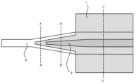
- FIG. 2 is an enlarged plan view of the portion surrounded by the dotted line frame A in FIG. 1, showing an example of the configuration of the vicinity including the SSC.
- 3 is a cross-sectional view along the dotted line C-C' in FIG. 2
- FIG. 4 is a cross-sectional view along the dotted line B-B' in FIG. 2
- FIG. 5 is a cross-sectional view along the dotted line A-A' in FIG.
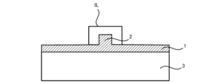
- FIG. 3 shows the same structure as the optical waveguide including the modulation section MP in the optical waveguide element, and the rib-type optical waveguide 2 is formed on part of the substrate 1 .
- a dielectric layer IL is arranged to cover the side and top surfaces of the optical waveguide 2 . Since the substrate 1 and the optical waveguide 2 are extremely thin layers, the reinforcing substrate 3 is arranged on the lower surface side of the substrate 1 in order to increase the mechanical strength.
- the width of the optical waveguide 2 and the substrate 1 has a tapered shape that gradually narrows toward the edge of the substrate. Therefore, in FIG. 3, the rib-shaped optical waveguide 2 functions as the core portion of the optical waveguide, but in FIG. 4, the rib-shaped optical waveguide 2 and the substrate 1 play the role of the core portion. Furthermore, in FIG. 5, the dielectric layer IL also serves as a core portion, and the MFD of the optical waveguide gradually expands. Since the MFD can be made smaller by narrowing the width of the dielectric layer in this way, the size of the MFD can be controlled to a desired size, and the optical insertion loss with the optical fiber or the like can be reduced.
- the width of the dielectric layer IL becomes narrower, and at the same time, the size of the cross-sectional area (surface area) occupied by the rib-type optical waveguide 2 and the substrate 1 also becomes smaller.
- the width of the dielectric layer IL becomes narrower, the adhesiveness between the dielectric layer IL and the substrate 1 (optical waveguide 2) and the adhesiveness between the dielectric layer IL and the reinforcing substrate 3 are lowered. Phenomena such as peeling and cracking of the body layer IL also occur. In particular, this phenomenon is remarkable in a portion where the width of the substrate 1 (optical waveguide 2) or the dielectric layer IL is narrow, such as SSC.
- Japanese Patent Application No. 2021-050409 filing date: March 24, 2021
- Japanese Patent Application No. 2020-165004 (Filing date: September 30, 2020)
- PCT/JP2021/032007 (Filing date: August 31, 2021)
- the problem to be solved by the present invention is to solve the above-described problems, and to provide an optical waveguide element having a dielectric layer covering an optical waveguide, in which problems such as peeling and cracking of the dielectric layer are suppressed. It is to provide a wave path element.
- a further object of the present invention is to provide an optical modulation device and an optical transmitter using the optical waveguide element.
- an optical waveguide element, an optical modulation device using the same, and an optical transmitter according to the present invention have the following technical features.
- the optical waveguide is a rib-type optical waveguide, and At least part of the side surface is characterized by a slope shape formed by a curved surface.
- the shape of the cross section perpendicular to the propagation direction of the light wave of the rib-type optical waveguide is trapezoidal, triangular, or a shape stacked in multiple stages, and At least part of the overhanging side is formed by a curved line.
- the optical waveguide element described in (1) or (2) above has a spot size conversion section including the rib type optical waveguide and the dielectric layer, and in the spot size conversion section, the substrate is The width of the rib-shaped optical waveguide decreases or increases toward the ends, and the dielectric layer functions as an optical waveguide.
- the optical waveguide element described in (1) to (3) above has a spot size conversion section including the rib-type optical waveguide and the dielectric layer, and in the spot size conversion section, the substrate is The thickness of the rib-type optical waveguide is made thinner or thicker toward the end, and the dielectric layer functions as an optical waveguide.
- the refractive index of the dielectric layer is smaller than the refractive index of the rib-type optical waveguide.
- the optical waveguide element according to any one of the above (1) to (5) is characterized in that the optical waveguide element is housed in a housing and comprises an optical fiber for inputting or outputting a light wave to or from the optical waveguide. It is an optical modulation device that
- the optical waveguide element has a modulation electrode for modulating the light wave propagating through the optical waveguide, and the modulation signal input to the modulation electrode of the optical waveguide element is It is characterized by having an electronic circuit for amplification inside the housing.
- An optical transmitter comprising the optical modulation device according to (6) or (7) above and an electronic circuit for outputting a modulation signal for causing the optical modulation device to perform a modulation operation.
- the present invention provides an optical waveguide element having an optical waveguide formed on a substrate and a dielectric layer covering the optical waveguide, wherein the optical waveguide is a rib-type optical waveguide, and along the longitudinal direction of the rib-type optical waveguide, Since at least a part of the side surface is curved and has a slope shape, the contact area between the dielectric layer and the rib-type optical waveguide can be increased. It is possible to suppress the occurrence of defects such as peeling and cracking of the.
- FIG. 1 is a plan view showing an example of an optical waveguide element having a dielectric layer covering an optical waveguide, disclosed in Patent Document 3;
- FIG. FIG. 2 is an enlarged plan view of a portion surrounded by a dotted line frame A in FIG. 1;
- 3 is a cross-sectional view taken along the dotted line C-C' in FIG. 2;
- FIG. 3 is a cross-sectional view along the dotted line B-B' in FIG. 2;
- FIG. 3 is a cross-sectional view along the dotted line A-A' in FIG. 2;
- FIG. FIG. 3 is a cross-sectional view taken along the dotted line A-A' in FIG. 2, showing the first embodiment according to the present invention;
- FIG. 3 is a cross-sectional view taken along the dotted line A-A' in FIG. 2, showing a second embodiment according to the present invention
- FIG. 3 is a cross-sectional view taken along the dotted line B-B' in FIG. 2, showing a third embodiment according to the present invention
- FIG. 3 is a cross-sectional view taken along the dotted line B-B' in FIG. 2, showing a fourth embodiment according to the present invention
- FIG. 4 is a cross-sectional view taken along the dotted line C-C' in FIG. 2, showing a fifth embodiment according to the present invention
- FIG. 10 is a diagram showing an application example (sixth embodiment) of the optical waveguide device of the present invention. It is a figure which shows the application example (7th Example) of the optical waveguide element of this invention. It is a figure which shows the application example (8th Example) of the optical waveguide element of this invention.
- 1 is a plan view for explaining an optical modulation device and an optical transmitter according to the present invention; FIG.
- the optical waveguide element of the present invention is an optical waveguide element having an optical waveguide 2 formed on a substrate 1 and a dielectric layer IL covering the optical waveguide, wherein the optical waveguide 2 is
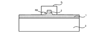
- the rib-type optical waveguide is characterized in that at least a part of the side surface along the longitudinal direction of the rib-type optical waveguide has a slope shape formed by curved surfaces (R1 to R9).
- the "rib-type optical waveguide” in the present invention means a portion having a convex cross-sectional shape and functioning as an optical waveguide, as shown in FIGS.
- the inside of the SSC, etc. may include not only the projecting portion 2 but also the substrate 1, as shown in FIGS. Further, there may be only substrate 1, as in FIGS.
- the "rib type optical waveguide” does not include the dielectric layer IL.
- the material 1 having an electro-optical effect used in the optical waveguide device of the present invention includes substrates such as lithium niobate (LN), lithium tantalate (LT), PLZT (lead lanthanum zirconate titanate), and substrates thereof.
- substrates such as lithium niobate (LN), lithium tantalate (LT), PLZT (lead lanthanum zirconate titanate), and substrates thereof.
- Substrates with magnesium doped materials can be used.
- Vapor deposition films made of these materials can also be used.
- Various materials such as semiconductor materials and organic materials can also be used as optical waveguides.
- the substrate 1 other than the optical waveguide is etched, grooves are formed on both sides of the optical waveguide, or a rib-type optical waveguide is formed on the substrate with a convex portion corresponding to the optical waveguide. It is possible to use Furthermore, it is also possible to increase the refractive index of the substrate surface by thermal diffusion of Ti or the like, proton exchange, or the like, in accordance with the rib type optical waveguide.
- the thickness of the substrate (thin plate) 1 on which the optical waveguide 2 is formed is set to 10 ⁇ m or less, more preferably 5 ⁇ m or less, still more preferably 1 ⁇ m or less, in order to achieve velocity matching between the microwave and the light wave of the modulated signal.
- the height of the rib type optical waveguide is set to 4 ⁇ m or less, more preferably 3 ⁇ m or less, further preferably 1 ⁇ m or less or 0.4 ⁇ m or less. It is also possible to form a vapor deposition film on the reinforcing substrate 3 and process the film into the shape of an optical waveguide.
- the substrate on which the optical waveguide is formed is adhesively fixed to the reinforcing substrate 3 through direct bonding or an adhesive layer such as resin as shown in FIGS. 3 to 10 in order to increase mechanical strength.
- a material having a refractive index lower than that of the optical waveguide or the substrate on which the optical waveguide is formed and a material having a coefficient of thermal expansion close to that of the optical waveguide, such as a substrate containing an oxide layer such as crystal or glass is suitable.
- Composite substrates in which a silicon oxide layer is formed on a silicon substrate, or a silicon oxide layer is formed on an LN substrate, which are abbreviated as SOI and LNOI, can also be used.
- the optical waveguide 2 in FIG. 2 is covered with a dielectric layer (insulating film) IL disclosed in Patent Document 1.
- a dielectric layer (insulating film) IL disclosed in Patent Document 1.
- the dielectric layer IL is preferably a dielectric with a refractive index greater than 1, and is set to 0.5 times or more and 0.75 times or less the refractive index of the optical waveguide 2 .
- the thickness of the dielectric layer IL is not particularly limited, it can be formed up to a thickness of about 10 ⁇ m.
- the optical waveguide portion including the modulating portion MP that modulates the light wave by applying a modulation signal to the optical waveguide 2
- the optical waveguide 2 functions as a core portion and the dielectric layer functions as a cladding portion.
- the dielectric layer IL can be formed by a sputtering method or a CVD method using an inorganic material such as SiO2 , but an organic material such as resin may also be used.
- a photoresist containing a coupling agent can be used, and a so-called photosensitive insulating film (permanent resist), which is cured by thermal crosslinking reaction, can be used.
- the resin it is also possible to use other materials such as polyamide resin, melamine resin, phenol resin, amino resin, and epoxy resin.
- the dielectric layer IL is arranged across the optical waveguide 2 (on the right side of the drawing) and the spot size converter SSC (on the left side of the drawing).
- the present invention is not limited to such an example, and it is also possible to use different dielectric layers on the optical waveguide side and the SSC side. However, if the dielectric layers have different refractive indices, light wave propagation loss is likely to occur at the boundary between the dielectric layers. It should be set to 5 or less. More preferably, the dielectric layer IL covering the optical waveguide continuously enters the spot size conversion section as a part of the dielectric layer forming the spot size conversion section from the modulation section side of the optical waveguide. More preferably, the dielectric layer of the optical waveguide on the modulation section side and part of the dielectric layer forming the spot size conversion section are simultaneously formed in the same manufacturing process.
- the dielectric layer IL functions together with the optical waveguide 2 and the substrate 1 as part of the optical waveguide, especially as the core portion of the optical waveguide.
- the width of the dielectric layer IL forming the SSC in FIG. 2 is tapered from the viewpoint of mode diameter conversion and light confinement. At the leftmost position in FIG. 2, the width is about 5 ⁇ m. On the other hand, in the modulation section, the width of the dielectric layer IL is 10 ⁇ m or more from the viewpoint of adhesion and the like, and therefore the lateral width of the dielectric layer IL is wider in the modulation section than in the SSC.
- the width of the optical waveguide (protruding portion 2) and the substrate 1 are gradually changed in a tapered shape, but the present invention is not limited to this, and the thickness of the optical waveguide 2 and the substrate 1 can be gradually reduced or increased. may be used, or a combination of the two may be used.
- the feature of the optical waveguide element of the present invention is that, as shown in FIGS. 6 to 13, at least a part of the side surface along the longitudinal direction of the rib type optical waveguide has a slope shape formed by curved surfaces (R1 to R9). be.
- curved surfaces curved boundary line in the cross-sectional view
- the contact area between the dielectric layer and the rib-type optical waveguide is increased, and the adhesion between the two can be enhanced.
- the substrate 1 plays the role of a rib-type optical waveguide, and curved surfaces R1 are formed on its side surfaces.
- the cross-sectional shape of the rib-type optical waveguide is substantially triangular.
- the cross-sectional shape of the rib-type optical waveguide (substrate 1) is substantially trapezoidal.
- a curved surface R2 is formed on a laterally protruding side (side) of the trapezoid.
- the cross-sectional shape of the rib-type optical waveguide in the present invention (the cross-sectional shape perpendicular to the propagation direction of the light wave) is trapezoidal, triangular, or a shape stacked in multiple stages, and at least a portion of the laterally projecting sides are curved. It is sufficient if it is formed by
- the third embodiment of FIG. 8 has a shape in which trapezoids are stacked, and a curved surface R3 is provided on the lower side surface of the trapezoid.
- curved surfaces R4 and R5 are formed on the upper and lower trapezoidal side surfaces. 8 and 9 are cross sections taken along the dotted line BB' in FIG. It is also possible to form it in the wave path (convex part 2).
- a curved surface R6 is formed on the trapezoidal side surface of the convex portion 2 (rib type optical waveguide) formed on the substrate 1.
- a curved surface R7 is formed in a part of a plurality of steps, and as shown in FIG. A curved surface R8 is also possible.
- FIG. 13 it is also possible to form a curved surface R9 that bulges outward.
- a desired etching mask having a curved surface is patterned, and a dry etching method such as reactive ion etching (RIE) or a suitable etchant is used. It can be performed by a wet etching method or the like.
- RIE reactive ion etching
- the optical waveguide element of the present invention is provided with a modulation electrode that modulates the light wave propagating through the optical waveguide 2, and is accommodated in the housing CA as shown in FIG. Furthermore, by providing an optical fiber (F) for inputting and outputting light waves in the optical waveguide, the optical modulation device MD can be configured.
- the optical fiber F is optically coupled to the optical waveguide within the optical waveguide element using the optical lens 4 .
- the optical fiber may be introduced into the housing via a through-hole penetrating the side wall of the housing and directly joined to the optical waveguide element.
- An optical transmitter OTA can be configured by connecting an electronic circuit (digital signal processor DSP) that outputs a modulation signal that causes the optical modulation device MD to perform a modulation operation, to the optical modulation device MD.
- DSP digital signal processor
- a driver circuit DRV is used because the modulated signal applied to the optical waveguide device must be amplified.
- the driver circuit DRV and the digital signal processor DSP can be arranged outside the housing CA, but can also be arranged inside the housing CA. In particular, by arranging the driver circuit DRV inside the housing, it is possible to further reduce the propagation loss of the modulated signal from the driver circuit.
Landscapes
- Physics & Mathematics (AREA)
- Nonlinear Science (AREA)
- General Physics & Mathematics (AREA)
- Optics & Photonics (AREA)
- Engineering & Computer Science (AREA)
- Chemical & Material Sciences (AREA)
- Ceramic Engineering (AREA)
- Crystallography & Structural Chemistry (AREA)
- Electromagnetism (AREA)
- Microelectronics & Electronic Packaging (AREA)
- Optical Modulation, Optical Deflection, Nonlinear Optics, Optical Demodulation, Optical Logic Elements (AREA)
- Optical Integrated Circuits (AREA)
Abstract
Description
特許文献1では、このような不具合を解消するため、光導波路を覆う誘電体層(絶縁膜)を設けることが提案されている。
(1) 基板に形成される光導波路と、該光導波路を覆う誘電体層とを有する光導波路素子において、該光導波路はリブ型光導波路であり、該リブ型光導波路の長手方向に沿った側面の少なくとも一部は、曲面で形成されるスロープ形状であることを特徴とする。
本発明の光導波路素子は、図6乃至13に示すように、基板1に形成される光導波路2と、該光導波路を覆う誘電体層ILとを有する光導波路素子において、該光導波路2はリブ型光導波路であり、該リブ型光導波路の長手方向に沿った側面の少なくとも一部は、曲面(R1~R9)で形成されるスロープ形状であることを特徴とする。
また、半導体材料や有機材料など種々の材料も光導波路として利用可能である。
誘電体層ILとしては、屈折率が1より大きい誘電体であることが好ましく、光導波路2の屈折率の0.5倍以上、0.75倍以下に設定される。誘電体層ILの厚さは特に限定されないが、10μm程度の厚さまで形成することが可能である。光導波路2に変調信号を印加して光波を変調する変調部MPを含む光導波路部分(SSCを除く)では、光導波路2はコア部として、誘電体層はクラッド部として機能する。
また、図7の第2実施例では、リブ型光導波路(基板1)の断面形状は略台形となっている。台形の横方向に張り出した辺(側辺)に曲面R2が形成されている。
さらには、図11に示すように、複数段の一部分に曲面R7を形成したり、図12に示すように、同じ側面でも一部を平面(断面の境界は直線)とし、他の一部を曲面R8とすることも可能である。図13に示すように外側に膨らみを持つ曲面R9とすることも可能性である。
2 光導波路
IL 誘電体層
MP 変調部
SSC スポットサイズ変換部
Claims (8)
- 基板に形成される光導波路と、該光導波路を覆う誘電体層とを有する光導波路素子において、
該光導波路はリブ型光導波路であり、該リブ型光導波路の長手方向に沿った側面の少なくとも一部は、曲面で形成されるスロープ形状であることを特徴とする光導波路素子。 - 請求項1に記載の光導波路素子において、該リブ型光導波路の光波の伝搬方向に垂直な断面の形状が、台形、三角形、または複数段に積み重ねた形状であり、横方向に張り出した辺の少なくとも一部は曲線で形成されていることを特徴とする光導波路素子。
- 請求項1又は2に記載の光導波路素子において、該リブ型光導波路と該誘電体層とを含むスポットサイズ変換部を有し、該スポットサイズ変換部では、該基板の端部に向かって該リブ型光導波路の幅が減少または増加すると共に、該誘電体層が光導波路として機能することを特徴とする光導波路素子。
- 請求項1乃至3に記載の光導波路素子において、該リブ型光導波路と該誘電体層とを含むスポットサイズ変換部を有し、該スポットサイズ変換部では、該基板の端部に向かって該リブ型光導波路の厚さを薄くするまたは厚くすると共に、該誘電体層が光導波路として機能することを特徴とする光導波路素子。
- 請求項1乃至4のいずれかに記載の光導波路素子において、該誘電体層の屈折率は、該リブ型光導波路の屈折率よりも小さいことを特徴とする光導波路素子。
- 請求項1乃至5いずれかに記載の光導波路素子は、
該光導波路素子は筐体内に収容され、
該光導波路に光波を入力又は出力する光ファイバを備えることを特徴とする光変調デバイス。 - 請求項6に記載の光変調デバイスにおいて、
該光導波路素子は該光導波路を伝搬する光波を変調するための変調電極を備え、
該光導波路素子の変調電極に入力する変調信号を増幅する電子回路を該筐体の内部に有することを特徴とする光変調デバイス。 - 請求項6又は7に記載の光変調デバイスと、
該光変調デバイスに変調動作を行わせる変調信号を出力する電子回路とを有することを特徴とする光送信装置。
Priority Applications (4)
| Application Number | Priority Date | Filing Date | Title |
|---|---|---|---|
| CN202180088363.3A CN116830024A (zh) | 2021-09-30 | 2021-09-30 | 光波导元件及使用所述光波导元件的光调制器件以及光发送装置 |
| US18/281,107 US20240231134A1 (en) | 2021-09-30 | 2021-09-30 | Optical waveguide element, and optical modulation device and optical transmission apparatus which use same |
| JP2023550961A JP7670153B2 (ja) | 2021-09-30 | 2021-09-30 | 光導波路素子及びそれを用いた光変調デバイス並びに光送信装置 |
| PCT/JP2021/036277 WO2023053404A1 (ja) | 2021-09-30 | 2021-09-30 | 光導波路素子及びそれを用いた光変調デバイス並びに光送信装置 |
Applications Claiming Priority (1)
| Application Number | Priority Date | Filing Date | Title |
|---|---|---|---|
| PCT/JP2021/036277 WO2023053404A1 (ja) | 2021-09-30 | 2021-09-30 | 光導波路素子及びそれを用いた光変調デバイス並びに光送信装置 |
Publications (1)
| Publication Number | Publication Date |
|---|---|
| WO2023053404A1 true WO2023053404A1 (ja) | 2023-04-06 |
Family
ID=85782087
Family Applications (1)
| Application Number | Title | Priority Date | Filing Date |
|---|---|---|---|
| PCT/JP2021/036277 Ceased WO2023053404A1 (ja) | 2021-09-30 | 2021-09-30 | 光導波路素子及びそれを用いた光変調デバイス並びに光送信装置 |
Country Status (4)
| Country | Link |
|---|---|
| US (1) | US20240231134A1 (ja) |
| JP (1) | JP7670153B2 (ja) |
| CN (1) | CN116830024A (ja) |
| WO (1) | WO2023053404A1 (ja) |
Citations (3)
| Publication number | Priority date | Publication date | Assignee | Title |
|---|---|---|---|---|
| JPH08316219A (ja) * | 1995-05-19 | 1996-11-29 | Nec Corp | 半導体装置の製造方法 |
| JP2011075917A (ja) * | 2009-09-30 | 2011-04-14 | Sumitomo Osaka Cement Co Ltd | 光導波路素子 |
| US20190346625A1 (en) * | 2018-05-08 | 2019-11-14 | Shanghai Institute of Optics And Fine Mechanics, Chiness Academy of Sciences | Method for preparing film micro-optical structure based on photolithography and chemomechanical polishing |
Family Cites Families (4)
| Publication number | Priority date | Publication date | Assignee | Title |
|---|---|---|---|---|
| JP3976514B2 (ja) * | 2001-04-05 | 2007-09-19 | 日本電気株式会社 | 光導波路の製造方法 |
| CA2349031A1 (en) * | 2001-05-28 | 2002-11-28 | Optenia, Inc. | Method of fabricating mode-size converter with three dimensional tapered with high processing tolerance |
| WO2011019887A2 (en) * | 2009-08-14 | 2011-02-17 | Massachusetts Institute Of Technology | Waveguide coupler having continuous three-dimensional tapering |
| JP2017129834A (ja) * | 2015-08-21 | 2017-07-27 | Tdk株式会社 | 光導波路素子およびこれを用いた光変調器 |
-
2021
- 2021-09-30 US US18/281,107 patent/US20240231134A1/en active Pending
- 2021-09-30 JP JP2023550961A patent/JP7670153B2/ja active Active
- 2021-09-30 WO PCT/JP2021/036277 patent/WO2023053404A1/ja not_active Ceased
- 2021-09-30 CN CN202180088363.3A patent/CN116830024A/zh active Pending
Patent Citations (3)
| Publication number | Priority date | Publication date | Assignee | Title |
|---|---|---|---|---|
| JPH08316219A (ja) * | 1995-05-19 | 1996-11-29 | Nec Corp | 半導体装置の製造方法 |
| JP2011075917A (ja) * | 2009-09-30 | 2011-04-14 | Sumitomo Osaka Cement Co Ltd | 光導波路素子 |
| US20190346625A1 (en) * | 2018-05-08 | 2019-11-14 | Shanghai Institute of Optics And Fine Mechanics, Chiness Academy of Sciences | Method for preparing film micro-optical structure based on photolithography and chemomechanical polishing |
Non-Patent Citations (3)
| Title |
|---|
| H. HU ; R. RICKEN ; W. SOHLER ; R. B. WEHRSPOHN: "Lithium Niobate Ridge Waveguides Fabricated by Wet Etching", IEEE PHOTONICS TECHNOLOGY LETTERS, vol. 4, no. 6, 15 March 2007 (2007-03-15), USA, pages 417 - 419, XP011172151, ISSN: 1041-1135 * |
| LI YING, LAN TIAN, LI JING, WANG ZHIYONG: "High-efficiency edge-coupling based on lithium niobate on an insulator wire waveguide", APPLIED OPTICS, vol. 59, no. 22, 1 August 2020 (2020-08-01), US , pages 6694 - 6701, XP093042015, ISSN: 1559-128X, DOI: 10.1364/AO.395897 * |
| WU RONGBO, WANG MIN, XU JIAN, QI JIA, CHU WEI, FANG ZHIWEI, ZHANG JIANHAO, ZHOU JUNXIA, QIAO LINGLING, CHAI ZHIFANG, LIN JINTIAN, : "Long Low-Loss-Litium Niobate on Insulator Waveguides with Sub-Nanometer Surface Roughness", NANOMATERIALS, vol. 8, no. 11, pages 910, XP093054202, DOI: 10.3390/nano8110910 * |
Also Published As
| Publication number | Publication date |
|---|---|
| JPWO2023053404A1 (ja) | 2023-04-06 |
| JP7670153B2 (ja) | 2025-04-30 |
| US20240231134A1 (en) | 2024-07-11 |
| CN116830024A (zh) | 2023-09-29 |
Similar Documents
| Publication | Publication Date | Title |
|---|---|---|
| JP7540274B2 (ja) | 光導波路素子及びそれを用いた光変調デバイス並びに光送信装置 | |
| US11378828B2 (en) | Optical waveguide device | |
| JP2009244812A (ja) | 光導波路素子 | |
| US12422628B2 (en) | Optical waveguide element, and optical modulation device and optical transmission apparatus using same | |
| JP7666070B2 (ja) | 光導波路素子及びそれを用いた光変調デバイス並びに光送信装置 | |
| CN116194828B (zh) | 光波导元件及使用其的光调制器件和光发送装置 | |
| JP7670153B2 (ja) | 光導波路素子及びそれを用いた光変調デバイス並びに光送信装置 | |
| WO2023188311A1 (ja) | 光導波路素子及びそれを用いた光変調デバイス並びに光送信装置 | |
| WO2023032050A1 (ja) | 光導波路素子及びそれを用いた光変調デバイス並びに光送信装置 | |
| US12607803B2 (en) | Optical waveguide element, and optical transmission apparatus and optical modulation device using same | |
| CN221378428U (zh) | 光波导元件、使用光波导元件的光调制器件及光发送装置 | |
| CN118409391A (zh) | 光波导元件、使用光波导元件的光调制器件及光发送装置 | |
| WO2024069952A1 (ja) | 光導波路素子及びそれを用いた光変調デバイス並びに光送信装置 | |
| WO2025203274A1 (ja) | 光導波路素子及びそれを用いた光変調器並びに光送信装置 | |
| WO2023053332A1 (ja) | 光導波路素子及びそれを用いた光変調デバイス並びに光送信装置 | |
| WO2024201876A1 (ja) | 光導波路素子とそれを用いた光変調デバイス並びに光送信装置 | |
| WO2024075277A1 (ja) | 光導波路素子及びそれを用いた光変調器並びに光送信装置 |
Legal Events
| Date | Code | Title | Description |
|---|---|---|---|
| 121 | Ep: the epo has been informed by wipo that ep was designated in this application |
Ref document number: 21959439 Country of ref document: EP Kind code of ref document: A1 |
|
| WWE | Wipo information: entry into national phase |
Ref document number: 2023550961 Country of ref document: JP |
|
| WWE | Wipo information: entry into national phase |
Ref document number: 202180088363.3 Country of ref document: CN |
|
| WWE | Wipo information: entry into national phase |
Ref document number: 18281107 Country of ref document: US |
|
| NENP | Non-entry into the national phase |
Ref country code: DE |
|
| 122 | Ep: pct application non-entry in european phase |
Ref document number: 21959439 Country of ref document: EP Kind code of ref document: A1 |