WO2023053303A1 - Light source unit, optical transmission module, and pluggable optical module - Google Patents
Light source unit, optical transmission module, and pluggable optical module Download PDFInfo
- Publication number
- WO2023053303A1 WO2023053303A1 PCT/JP2021/035996 JP2021035996W WO2023053303A1 WO 2023053303 A1 WO2023053303 A1 WO 2023053303A1 JP 2021035996 W JP2021035996 W JP 2021035996W WO 2023053303 A1 WO2023053303 A1 WO 2023053303A1
- Authority
- WO
- WIPO (PCT)
- Prior art keywords
- optical
- drive signal
- light
- signal
- outputs
- Prior art date
Links
- 230000003287 optical effect Effects 0.000 title claims abstract description 200
- 230000005540 biological transmission Effects 0.000 title claims description 44
- 238000001514 detection method Methods 0.000 claims abstract description 25
- 239000004065 semiconductor Substances 0.000 claims description 18
- XUIMIQQOPSSXEZ-UHFFFAOYSA-N Silicon Chemical compound [Si] XUIMIQQOPSSXEZ-UHFFFAOYSA-N 0.000 claims description 16
- 229910052710 silicon Inorganic materials 0.000 claims description 16
- 239000010703 silicon Substances 0.000 claims description 16
- 239000013307 optical fiber Substances 0.000 claims description 14
- 238000004891 communication Methods 0.000 claims description 7
- 230000000737 periodic effect Effects 0.000 claims description 7
- 230000010355 oscillation Effects 0.000 abstract description 8
- 238000000034 method Methods 0.000 description 5
- 239000000758 substrate Substances 0.000 description 5
- 239000003990 capacitor Substances 0.000 description 4
- 230000008859 change Effects 0.000 description 4
- 238000010586 diagram Methods 0.000 description 4
- 238000010438 heat treatment Methods 0.000 description 4
- 239000011248 coating agent Substances 0.000 description 3
- 238000000576 coating method Methods 0.000 description 3
- 230000001902 propagating effect Effects 0.000 description 3
- 238000012546 transfer Methods 0.000 description 3
- 238000012544 monitoring process Methods 0.000 description 2
- 230000008569 process Effects 0.000 description 2
- 238000012545 processing Methods 0.000 description 2
- 230000003321 amplification Effects 0.000 description 1
- 230000000295 complement effect Effects 0.000 description 1
- 230000008878 coupling Effects 0.000 description 1
- 238000010168 coupling process Methods 0.000 description 1
- 238000005859 coupling reaction Methods 0.000 description 1
- 230000007423 decrease Effects 0.000 description 1
- 238000005516 engineering process Methods 0.000 description 1
- 239000000835 fiber Substances 0.000 description 1
- 238000002347 injection Methods 0.000 description 1
- 239000007924 injection Substances 0.000 description 1
- 238000003780 insertion Methods 0.000 description 1
- 230000037431 insertion Effects 0.000 description 1
- 239000012212 insulator Substances 0.000 description 1
- 229910044991 metal oxide Inorganic materials 0.000 description 1
- 150000004706 metal oxides Chemical class 0.000 description 1
- 238000003199 nucleic acid amplification method Methods 0.000 description 1
- 230000010287 polarization Effects 0.000 description 1
- 230000002250 progressing effect Effects 0.000 description 1
- 230000009467 reduction Effects 0.000 description 1
- 230000003595 spectral effect Effects 0.000 description 1
Images
Classifications
-
- G—PHYSICS
- G02—OPTICS
- G02F—OPTICAL DEVICES OR ARRANGEMENTS FOR THE CONTROL OF LIGHT BY MODIFICATION OF THE OPTICAL PROPERTIES OF THE MEDIA OF THE ELEMENTS INVOLVED THEREIN; NON-LINEAR OPTICS; FREQUENCY-CHANGING OF LIGHT; OPTICAL LOGIC ELEMENTS; OPTICAL ANALOGUE/DIGITAL CONVERTERS
- G02F1/00—Devices or arrangements for the control of the intensity, colour, phase, polarisation or direction of light arriving from an independent light source, e.g. switching, gating or modulating; Non-linear optics
- G02F1/01—Devices or arrangements for the control of the intensity, colour, phase, polarisation or direction of light arriving from an independent light source, e.g. switching, gating or modulating; Non-linear optics for the control of the intensity, phase, polarisation or colour
Definitions
- the present invention relates to a light source unit, an optical transmission module and a pluggable optical module.
- pluggable optical modules are progressing in optical communication systems with standards such as SFP (Small Form Factor Pluggable) and XFP (10-Gigabit Small Form Factor Pluggable).
- a pluggable optical module is an optical transceiver that can be inserted into and removed from a socket of an optical transmission device.
- the pluggable optical module receives control information from the optical transmission device on the host side. Then, the operation of the pluggable optical module is switched or changed according to the received control information.
- An optical module (optical transceiver) including a pluggable optical module is provided with an optical transmission module that transmits an optical signal.
- the optical transmission module includes a light source that outputs laser light and a modulator that modulates the laser light into an optical signal. and are provided (Patent Documents 1 and 2).
- a wavelength tunable light source As a light source, a wavelength tunable light source is often used.
- a wavelength tunable light source when setting or changing the wavelength (channel), the wavelength and phase of the output laser light are controlled.
- a control method is known in which a low-frequency dither signal is used to monitor the amplitude of the laser beam according to the dither signal to adjust the phase (Patent Documents 1 to 4).
- Patent Documents 2 and 4 It is known that a sine wave signal is generally used as the dither signal (Patent Documents 2 and 4). However, generating a periodic analog signal such as a sinusoidal signal requires a relatively complicated circuit (Patent Document 4).
- the package size is defined by the standard, and in order to implement the necessary functions, miniaturization of the components of the optical transceiver is required. , low power consumption is required.
- a dither signal that is advantageous for downsizing the optical transceiver and phase control of the laser light output from the wavelength tunable light source using the dither signal.
- the present invention has been made in view of the above circumstances, and it is an object of the present invention to control the phase of laser light output from a light source unit using a square-wave dither signal.
- a light source unit which is an aspect of the present invention, includes a semiconductor optical amplifier that amplifies input light, and an optical resonator in which the light reciprocates together with the semiconductor optical amplifier, and the wavelength of the light that is transmitted is variable.
- An external resonator having a tunable filter and outputting laser light that has been oscillated by the optical resonator and transmitted through the tunable filter, and an optical waveguide provided in the external resonator through which the light propagates.
- a heater for controlling the phase of the laser light; a drive signal output section for outputting a drive signal to the heater; a control section for controlling the drive signal given to the heater by the drive signal output section; an optical monitor unit for monitoring intensity, wherein the control unit controls the drive signal output unit so that a dither signal composed of a periodic rectangular wave is superimposed on the drive signal; detecting the amplitude of variation in the intensity of the laser light caused by the dither signal and outputting the detection result to the control section, the control section controlling the drive signal output section so that the power of the drive signal is changed; While controlling, the detection result of the light monitor unit is monitored, the power when the amplitude of the fluctuation of the intensity of the laser light is minimized is searched, and the searched minimum power is determined as the power of the drive signal. It is something to do.
- An optical transmission module includes a light source unit that outputs laser light, and an optical modulator that modulates the laser light according to a data signal and outputs an optical signal, wherein the light source unit a semiconductor optical amplifier that amplifies input light; and a wavelength tunable filter that constitutes an optical resonator through which the light reciprocates together with the semiconductor optical amplifier and that allows the wavelength of light to be transmitted to be variable, and the optical resonator. and controlling the phase of the laser light provided in an external resonator for outputting the laser light transmitted through the wavelength tunable filter and an optical waveguide provided in the external resonator for propagating the light.
- a heater a drive signal output unit that outputs a drive signal to the heater, a control unit that controls the drive signal that the drive signal output unit gives to the heater, a light monitor unit that monitors the intensity of the laser light, wherein the control unit controls the drive signal output unit so that a dither signal composed of a periodic rectangular wave is superimposed on the drive signal, and the optical monitor unit controls the laser light generated by the dither signal. and outputs the detection result to the control section, and the control section controls the drive signal output section so as to change the power of the drive signal while controlling the light monitor section.
- the detection result is monitored, the power at which the amplitude of the fluctuation of the intensity of the laser beam becomes the minimum is searched, and the searched minimum power is determined as the power of the drive signal.
- a pluggable optical module which is one aspect of the present invention, comprises a pluggable electrical connector configured to be insertable/removable to/from an optical transmission device and capable of two-way communication with the optical transmission device; an optical transmission module for outputting an optical signal based on a data signal input from the optical transmission device; an optical reception module for demodulating the input optical signal and outputting the demodulated signal to the optical transmission device; a pluggable optical receptor configured to allow insertion and removal of a fiber, outputting the optical signal input from the optical transmission module to the optical fiber, and outputting the input optical signal input from the optical fiber to the optical reception module; wherein the optical transmission module comprises a light source unit for outputting a laser beam, and an optical modulator for modulating the laser beam according to the data signal and outputting an optical signal, the light source unit comprising: a semiconductor optical amplifier that amplifies input light; and a wavelength tunable filter that constitutes an optical resonator through which the light reciprocates together with the semiconductor optical amplifier and that allows the wavelength of light to
- a drive signal output unit for outputting a drive signal to the heater; a control unit for controlling the drive signal provided to the heater by the drive signal output unit; and a light monitor unit for monitoring the intensity of the laser beam.
- the control section controls the drive signal output section so that a dither signal composed of a periodic rectangular wave is superimposed on the drive signal; The amplitude of intensity fluctuation is detected, the detection result is output to the control section, and the control section controls the drive signal output section so that the power of the drive signal is changed while performing the detection of the optical monitor section. The results are monitored, the power at which the amplitude of the fluctuation of the intensity of the laser light becomes the minimum is searched, and the searched minimum power is determined as the power of the drive signal.
- the phase of the output laser light can be controlled using the square-wave dither signal.
- FIG. 1 is a diagram schematically showing a configuration of a pluggable optical module according to Embodiment 1;
- FIG. 1 is a diagram schematically showing a configuration example of an optical transmission module according to a first embodiment;
- FIG. 1 is a diagram schematically showing the configuration of a light source unit according to Embodiment 1;
- FIG. 10 is a diagram showing changes in the intensity and wavelength of monitor light when the power supplied to the heater is changed by a driving signal superimposed with a dither signal;
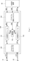
- FIG. 1 schematically shows the configuration of a pluggable optical module 100 according to the first embodiment.
- the pluggable optical module 100 is controlled based on the control signal CON input from the optical transmission device 90, which is the communication host.
- the pluggable optical module 100 can receive the modulated signal MOD, which is a data signal, from the optical transmission device 90 together with the control signal CON, and output the optical signal LS1 modulated based on the modulated signal MOD to the optical fiber 81 .
- the pluggable optical module 100 can also receive the optical signal LS2 input from the optical fiber 82 and output the data signal DAT obtained by demodulating the optical signal LS2 to the optical transmission device 90 .
- the optical transmission device 90 performs communication data processing such as frame processing of a communication data signal from the pluggable optical module 100 or a communication data signal input to the pluggable optical module 100, for example.
- the pluggable optical module 100 has an optical transmission module 101 , an optical reception module 102 , a control section 103 , a pluggable electrical connector 104 and a pluggable optical receptor 105 .
- the pluggable electrical connector 104 is configured to be removable from the optical transmission device 90 .
- the pluggable electrical connector 104 receives the control signal CON, which is an electrical signal output from the optical transmission device 90 , and transfers it to the control unit 103 .
- the pluggable electrical connector 104 also receives the modulated signal MOD, which is an electrical signal output from the optical transmission device 90 , and transfers it to the optical transmission module 101 .
- the pluggable electrical connector 104 may transfer electrical signals output from the control section 103 to the optical transmission device 90 .
- the pluggable optical receptor 105 is configured such that a connector portion of an optical fiber 81 with a connector for transmission and a connector of an optical fiber 82 with a connector for reception can be inserted and removed.
- As connectors for the optical fibers 82 and 82 with connectors for example, LC type connectors or MU type connectors can be used.
- the pluggable optical receptor 105 transmits the optical signal LS1 output from the optical transmission module 101 to the optical fiber 81 and transmits the optical signal LS2 input from the optical fiber 82 to the optical reception module 102 .
- control unit 103 Based on the control signal CON input from the optical transmission device 90 via the pluggable electrical connector 104, the control unit 103 controls the operation of the optical transmission module 101 with the control signal CON1, and controls the operation of the optical reception module 102 with the control signal CON2. control behavior.
- the optical receiving module 102 demodulates the optical signal LS2 received via the pluggable optical receptor 105 into a data signal DAT, which is an electrical signal, and outputs the data signal DAT to the optical transmission device 90 via the pluggable electrical connector 104 .
- the optical receiver module 102 is configured to be able to demodulate the optical signal LS2 modulated by various modulation schemes.
- the optical transmission module 101 modulates the laser light output from the light source according to the modulation signal MOD, and outputs the optical signal LS1.
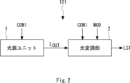
- FIG. 2 schematically shows a configuration example of the optical transmission module 101 according to the first embodiment.
- the optical transmission module 101 has a light source unit 1 and an optical modulation section 2 .
- the light source unit 1 is configured as a wavelength tunable optical module including a semiconductor optical device and a ring resonator, and outputs laser light L OUT of a predetermined wavelength to the optical modulator 2 .
- the optical modulation unit 2 is configured to have, for example, a Mach-Zehnder optical modulator and a drive circuit for driving it.
- the optical modulator 2 modulates the laser light L OUT according to the modulation signal MOD and outputs an optical signal LS1.
- the optical modulator 2 can modulate the optical signal LS1 by various modulation methods such as phase modulation, amplitude modulation, and polarization modulation, or by combining various modulation methods.
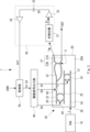
- FIG. 3 schematically shows the configuration of the light source unit 1 according to the first embodiment.
- the light source unit 1 has a semiconductor optical amplifier (hereinafter referred to as SOA) 10 , an external resonator 20 , an optical monitor section 30 , a drive signal output section 40 and a control section 50 .
- SOA semiconductor optical amplifier
- the SOA 10 is an active optical element that outputs light, and is configured as a semiconductor laser diode, for example.
- the SOA 10 is provided with an optical waveguide having a gain, for example, and emits laser light from the facet by laser oscillation by current injection or the like.
- the end surface 10A on the side of the external resonator 20 is coated with a low reflectance coating
- the opposite end surface 10B is coated with a high reflectance coating.
- the SOA 10 and the external resonator 20 are arranged with their waveguides aligned with each other, and the output light L, which is the laser beam of the SOA 10 , enters the external resonator 20 .
- the output light L has a certain spectral width, but its wavelength and phase can be adjusted by the external resonator 20, as will be described later.
- the external resonator 20 is configured as a resonator capable of resonating the output light L of the SOA 10 for laser oscillation and adjusting the wavelength and phase of the oscillated laser light L OUT .
- the external resonator 20 is a semiconductor device manufactured by silicon (Si) photonics technology, and is an external resonator having a wavelength tuning function.
- the external resonator 20 can be manufactured by a known Si process such as a CMOS (Complementary Metal Oxide Semiconductor) process.
- the configuration of the external resonator 20 will be described.
- the external resonator 20 has ring resonators 21 and 22, a loop mirror 23, silicon optical waveguides 24 to 26, an output optical waveguide 27, and heaters H1 to H3 formed on a substrate 20A.
- Ring resonators 21 and 22 are also referred to as first and second ring resonators, respectively.
- the substrate 20A is composed of, for example, a silicon substrate or an SOI (Silicon on Insulator) substrate.
- the silicon optical waveguides 24 to 26 are composed of thin wire waveguides or rib waveguides.
- the silicon optical waveguide 24 optically connects the incident end surface 28 and the ring resonator 21 .
- a silicon optical waveguide 25 optically connects between the ring resonator 21 and the ring resonator 22 .
- a silicon optical waveguide 26 optically connects between the ring resonator 22 and the loop mirror 23 .
- an anti-reflection coating (not shown) is formed on the end of the silicon optical waveguide 24 on the incident end face 28 side.
- the ring resonators 21 and 22 function as filters in which the wavelength of the transmitted light is variable, and the light resonates between the ring resonators 21 and 22 to cause laser oscillation.
- the ring resonators 21 and 22 are provided with heaters H1 and H2, respectively. By heating the silicon optical waveguide constituting the ring resonator 21 with the heater H1, the optical path length (in other words, the phase of propagating light) is changed, thereby controlling the wavelength of the light reflected by the ring resonator 21. be done.
- the optical path length (in other words, the phase of the propagating light) is changed, whereby the light reflected by the ring resonator 22 is changed.
- Wavelength is controlled.
- a heater H3 is provided in the silicon optical waveguide 26 between the loop mirror 23 and the ring resonator 22 .
- the optical path length of the silicon optical waveguide is changed. ) changes. Thereby, the phase of the laser light output from the resonator can be controlled.
- the heater H3 adjusts the phase of the laser reciprocating in the resonator formed between the end face 10B of the SOA 10 and the loop mirror so that the phase is in a positive feedback state, thereby continuing the laser oscillation. Moreover, the amplification of laser light can be maximized. In addition, the ring resonators 21 and 22 transmit only the laser light of the desired wavelength to the loop mirror 23, so that the laser light of the desired wavelength can be output as the laser light LOUT and the monitor light LM .
- the heaters H1-H3 are controlled by drive signals D1-D3 output from the drive signal output section 40, respectively.
- the curved portion of the loop mirror 23 is optically connected to the curved portion of the output optical waveguide 27 .
- the two silicon optical waveguides on both sides of the curved portion of the output optical waveguide 27 extend to the output end face 29, and most of the laser light incident on the loop mirror 23 is transferred to the output optical waveguide 27 by the coupling portion (coupler C).
- a portion of the laser beams other than the laser beams coupled to the laser beam output waveguide 27A are coupled to the monitor beam output waveguide 27B by the coupler C, and output as monitor beams LM . It is output to the monitor section 30 .
- the light monitor unit 30 is configured to monitor the intensity of the monitor light LM and output a detection dither signal DIT indicating the monitor result.
- the optical monitor section 30 has a photodetector 31 , a current-voltage converter 32 , a capacitor 33 and an amplifier 34 .
- the photodetector 31 detects the monitor light LM output from the external resonator 20 and outputs a signal indicating the intensity of the detected monitor light LM .
- the photodetector 31 is composed of, for example, a photodiode, and outputs a detection signal SI, which is a current signal indicating the intensity of the monitor light LM .
- the current-voltage converter 32 is composed of, for example, a TIA (Transimpedance Amplifier), converts the detection signal SI, which is a current signal, into a voltage signal SV and outputs the voltage signal SV.
- TIA Transimpedance Amplifier
- the voltage signal SV is input to the amplifier 34 via the capacitor 33 .
- a signal obtained by cutting the DC component from the voltage signal SV by the capacitor 33 is amplified by the amplifier 34 and then output to the control unit 50 as the detected dither signal DIT.
- the drive signal output unit 40 outputs drive signals D1 to D3 to the heaters H1 to H3, respectively, according to the control by the control unit 50.
- the configuration and operation of the light source unit 1 will be described below, focusing on the drive signal D3 applied to the heater H3.
- the drive signal output unit 40 can superimpose the applied dither signal on the drive signal D3 and output it.
- the dither signal superimposed on the driving signal is referred to as an applied dither signal for distinction, and is output from the optical monitor section 30 to detect the intensity amplitude generated in the laser light by the applied dither signal. This signal is referred to as the detection dither signal.
- the control unit 50 controls the drive signal output unit 40 with the signal S3 so that the drive signal D3 superimposed with the predetermined applied dither signal is output to the heater H3.
- the controller 50 can also control the drive signals D1 and D2 output to the heaters H1 and H2 by the signals S1 and 2.
- the control unit 50 controls heating by the heater H3 step by step in order to search for the optimum phase.
- the control unit 50 periodically changes the current of the drive signal D3 to be applied to the heater H3 within a range that does not affect the wavelength accuracy, thereby forming the applied dither signal.
- the applied dither signal is given as a rectangular wave with a predetermined cycle, and the amplitude of this rectangular wave changes stepwise.
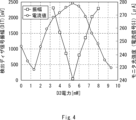
- FIG. 4 shows changes in the intensity and wavelength of the monitor light when the power supplied to the heater H3 is changed by the drive signal D3 on which the applied dither signal is superimposed.
- the power applied to the heater H3 is changed from 0 [mW] to 9+4/3 [mW] in approximately 2/3 [mW] increments, and accordingly the detection dither signal DIT output by the optical monitor unit 30 is changed.
- Monitor amplitude changes.
- the current signal SI output by the photodetector 31 changes in conjunction with the cycle of the applied dither signal.
- the power of the drive signal D3 is approximately 1 to 5 [mW] and 6 to 9 [mW], and in the region where the current signal varies greatly with respect to the power change, that is, in the region where the differential value of the current signal is large, the drive signal Variations in the current signal that accompany changes in the applied dither signal superimposed on D3 also increase.
- the amplitude of the detection dither signal DIT output from the optical monitor section 30 also increases.
- the power of the drive signal D3 is in the range of about 5 to 6 [mW], the region where the current signal changes little with respect to the power change near the top of the curve showing the current, that is, the differential value of the current signal In a small region, the variation of the current signal caused by the variation of the applied dither signal superimposed on the drive signal D3 is also small. As a result, the amplitude of the detection dither signal DIT output by the optical monitor section 30 also decreases.
- the phase of the laser light is optimal, that is, the maximum oscillation intensity of the external resonator 20. becomes.
- the control unit 50 searches for the power value when the amplitude of the detected dither signal DIT becomes the minimum, and sets the searched power value as the power of the drive signal D3, thereby maximizing the oscillation intensity of the external resonator 20.
- a point can be determined.
- the amplitude of the detected dither signal DIT is minimum when the power of the drive signal D3 is approximately 5.33 mW, so in this case the power of the drive signal D3 is set to approximately 5.33 mW.
- the Rukoto This makes it possible to keep the phase of the laser light L OUT output from the light source unit 1 in an optimum state thereafter.
- the execution of setting the drive signal D3 is not limited to this example, and may be performed when calibrating the phase of the laser light L OUT after starting the operation of the pluggable optical module, or in other cases. You can do it at any time.
- the drive signal output unit 40 may be configured as an analog-digital converter (hereinafter referred to as DAC).
- DAC analog-digital converter
- the control unit 50 outputs the analog signal on which the applied dither signal component is superimposed to the drive signal output unit 40 as the signal S3.
- the drive signal output unit 40 converts the signal S3 into a digital signal and outputs it as a drive signal D3, and the heater H3 is directly driven by the drive signal D3 which is a digital signal.
- Patent Documents 1 and 3 a heater is used to control the phase of light in the modulator, but the driving signal is given to the heater as an analog signal.
- a driver (the controller in Patent Document 1 and the setting unit in Patent Document 3) is provided for controlling the current supplied to the heater.
- a driver has a relatively large circuit scale, resulting in an increase in the size of the light source unit.
- the present invention is not limited to the above-described embodiments, and can be modified as appropriate without departing from the scope of the invention.
- the configuration of the above-described pluggable optical module (optical transceiver) is simplified for the purpose of describing the optical transceiver according to the above-described embodiments, and various other components may be included. Needless to say.
Abstract
An external resonator (20) outputs laser beam (LOUT) subjected to laser oscillation by an optical resonator constituted by the external resonator (20) and a SOA (10). A heater (H3) controls the phase of the laser beam (LOUT). A drive signal output unit (40) outputs a drive signal (D3) to the heater (H3). A control unit (50) controls the drive signal (D3) supplied to the heater (H3) by the drive signal output unit (40). An optical monitor unit (30) monitors the intensity of the laser beam (LOUT). The control unit (50) superimposes a square-wave applied dither signal onto the drive signal (D3). The optical monitor unit (30) detects the amplitude of the fluctuations in the laser beam (LOUT) due to the applied dither signal, and outputs the detection result. The control unit (50) changes the power of the drive signal (D3), monitors the detection result, finds the power at the minimum amplitude of the fluctuation in the laser beam (LOUT), and sets the power of the drive signal (D3) to the found power.
Description
本発明は、光源ユニット、光送信モジュール及びプラガブル光モジュールに関する。
The present invention relates to a light source unit, an optical transmission module and a pluggable optical module.
一方、例えばSFP(Small Form Factor Pluggable)やXFP(10-Gigabit Small Form Factor Pluggable)などの規格の光通信システムにおいて、プラガブル光モジュールの利用が進展している。プラガブル光モジュールは、光伝送装置のソケットに挿抜可能な光トランシーバである。プラガブル光モジュールの制御する場合、プラガブル光モジュールはホスト側である光伝送装置から制御情報を受け取る。そして、受け取った制御情報に応じて、プラガブル光モジュールの動作の切替えや変更が行われる。
On the other hand, the use of pluggable optical modules is progressing in optical communication systems with standards such as SFP (Small Form Factor Pluggable) and XFP (10-Gigabit Small Form Factor Pluggable). A pluggable optical module is an optical transceiver that can be inserted into and removed from a socket of an optical transmission device. When controlling the pluggable optical module, the pluggable optical module receives control information from the optical transmission device on the host side. Then, the operation of the pluggable optical module is switched or changed according to the received control information.
プラガブル光モジュールを含む光モジュール(光トランシーバ)においては、光信号を送信する光送信モジュールが設けられ、光送信モジュールには、レーザ光を出力する光源と、レーザ光を光信号に変調する変調器とが設けられる(特許文献1及び2)。
An optical module (optical transceiver) including a pluggable optical module is provided with an optical transmission module that transmits an optical signal. The optical transmission module includes a light source that outputs laser light and a modulator that modulates the laser light into an optical signal. and are provided (Patent Documents 1 and 2).
光源としては、波長可変光源がよく用いられるが、波長可変光源では、波長(チャネル)を設定又は変更する場合に、出力するレーザ光の波長及び位相の制御が行われる。例えば、位相を調整する場合には、低周波のディザ信号を用いて、ディザ信号によるレーザ光の振幅をモニタして位相を調整する制御手法が知られている(特許文献1~4)。
As a light source, a wavelength tunable light source is often used. In a wavelength tunable light source, when setting or changing the wavelength (channel), the wavelength and phase of the output laser light are controlled. For example, when adjusting the phase, a control method is known in which a low-frequency dither signal is used to monitor the amplitude of the laser beam according to the dither signal to adjust the phase (Patent Documents 1 to 4).
ディザ信号としては、一般的に正弦波信号が用いられることが知られている(特許文献2及び4)。しかし、正弦波信号のような周期的なアナログ信号を生成するには、比較的複雑な回路が必要となる(特許文献4)。
It is known that a sine wave signal is generally used as the dither signal (Patent Documents 2 and 4). However, generating a periodic analog signal such as a sinusoidal signal requires a relatively complicated circuit (Patent Document 4).
これに対し、10Gb/sの規格(SFP、XFP)で用いられる光トランシーバにおいては、規格によってパッケージの寸法が規定されており、必要な機能を実装するには、光トランシーバの構成部品の小型化、低消費電力化が求められる。
On the other hand, in the optical transceiver used in the 10 Gb/s standard (SFP, XFP), the package size is defined by the standard, and in order to implement the necessary functions, miniaturization of the components of the optical transceiver is required. , low power consumption is required.
よって、光トランシーバの小型化に有利なディザ信号と、ディザ信号を用いて波長可変光源が出力するレーザ光の位相制御の実現が望まれている。
Therefore, it is desired to realize a dither signal that is advantageous for downsizing the optical transceiver and phase control of the laser light output from the wavelength tunable light source using the dither signal.
本発明は、上記の事情に鑑みて成されたものであり、光源ユニットにおいて、矩形波のディザ信号を用いて出力するレーザ光の位相を制御することを目的とする。
The present invention has been made in view of the above circumstances, and it is an object of the present invention to control the phase of laser light output from a light source unit using a square-wave dither signal.
本発明の一態様である光源ユニットは、入力される光を増幅する半導体光増幅器と、前記半導体光増幅器とともに前記光が往復する光共振器を構成し、透過させる光の波長が可変である波長可変フィルタを有し、前記光共振器によって発振して前記波長可変フィルタを透過したレーザ光を出力する外部共振器と、前記光が伝搬する前記外部共振器に設けられた光導波路に設けられた、前記レーザ光の位相を制御するヒータと、前記ヒータへ駆動信号を出力する駆動信号出力部と、前記駆動信号出力部が前記ヒータへ与える前記駆動信号を制御する制御部と、前記レーザ光の強度をモニタする光モニタ部と、を備え、前記制御部は、周期的な矩形波からなるディザ信号が前記駆動信号に重畳されるように前記駆動信号出力部を制御し、前記光モニタ部は、前記ディザ信号により生じる前記レーザ光の強度の変動の振幅を検出し、検出結果を前記制御部へ出力し、前記制御部は、前記駆動信号の電力が変化するように前記駆動信号出力部を制御しながら前記光モニタ部の前記検出結果をモニタし、前記レーザ光の強度の変動の振幅が最小となるときの電力を探索し、前記探索した最小の電力を、前記駆動信号の電力として決定するものである。
A light source unit, which is an aspect of the present invention, includes a semiconductor optical amplifier that amplifies input light, and an optical resonator in which the light reciprocates together with the semiconductor optical amplifier, and the wavelength of the light that is transmitted is variable. An external resonator having a tunable filter and outputting laser light that has been oscillated by the optical resonator and transmitted through the tunable filter, and an optical waveguide provided in the external resonator through which the light propagates. a heater for controlling the phase of the laser light; a drive signal output section for outputting a drive signal to the heater; a control section for controlling the drive signal given to the heater by the drive signal output section; an optical monitor unit for monitoring intensity, wherein the control unit controls the drive signal output unit so that a dither signal composed of a periodic rectangular wave is superimposed on the drive signal; detecting the amplitude of variation in the intensity of the laser light caused by the dither signal and outputting the detection result to the control section, the control section controlling the drive signal output section so that the power of the drive signal is changed; While controlling, the detection result of the light monitor unit is monitored, the power when the amplitude of the fluctuation of the intensity of the laser light is minimized is searched, and the searched minimum power is determined as the power of the drive signal. It is something to do.
本発明の一態様である光送信モジュールは、レーザ光を出力する光源ユニットと、データ信号に応じて前記レーザ光を変調して光信号を出力する光変調部と、を備え、前記光源ユニットは、入力される光を増幅する半導体光増幅器と、前記半導体光増幅器とともに前記光が往復する光共振器を構成し、透過させる光の波長が可変である波長可変フィルタを有し、前記光共振器によって発振して前記波長可変フィルタを透過した前記レーザ光を出力する外部共振器と、前記光が伝搬する前記外部共振器に設けられた光導波路に設けられた、前記レーザ光の位相を制御するヒータと、前記ヒータへ駆動信号を出力する駆動信号出力部と、前記駆動信号出力部が前記ヒータへ与える前記駆動信号を制御する制御部と、前記レーザ光の強度をモニタする光モニタ部と、を備え、前記制御部は、周期的な矩形波からなるディザ信号が前記駆動信号に重畳されるように前記駆動信号出力部を制御し、前記光モニタ部は、前記ディザ信号により生じる前記レーザ光の強度の変動の振幅を検出し、検出結果を前記制御部へ出力し、前記制御部は、前記駆動信号の電力が変化するように前記駆動信号出力部を制御しながら前記光モニタ部の前記検出結果をモニタし、前記レーザ光の強度の変動の振幅が最小となるときの電力を探索し、前記探索した最小の電力を、前記駆動信号の電力として決定するものである。
An optical transmission module according to one aspect of the present invention includes a light source unit that outputs laser light, and an optical modulator that modulates the laser light according to a data signal and outputs an optical signal, wherein the light source unit a semiconductor optical amplifier that amplifies input light; and a wavelength tunable filter that constitutes an optical resonator through which the light reciprocates together with the semiconductor optical amplifier and that allows the wavelength of light to be transmitted to be variable, and the optical resonator. and controlling the phase of the laser light provided in an external resonator for outputting the laser light transmitted through the wavelength tunable filter and an optical waveguide provided in the external resonator for propagating the light. a heater, a drive signal output unit that outputs a drive signal to the heater, a control unit that controls the drive signal that the drive signal output unit gives to the heater, a light monitor unit that monitors the intensity of the laser light, wherein the control unit controls the drive signal output unit so that a dither signal composed of a periodic rectangular wave is superimposed on the drive signal, and the optical monitor unit controls the laser light generated by the dither signal. and outputs the detection result to the control section, and the control section controls the drive signal output section so as to change the power of the drive signal while controlling the light monitor section. The detection result is monitored, the power at which the amplitude of the fluctuation of the intensity of the laser beam becomes the minimum is searched, and the searched minimum power is determined as the power of the drive signal.
本発明の一態様であるプラガブル光モジュールは、光伝送装置に対して挿抜可能に構成され、前記光伝送装置との間で双方向通信が可能であるプラガブル電気コネクタと、前記プラガブル電気コネクタを介して前記光伝送装置から入力されるデータ信号に基づいて光信号を出力する光送信モジュールと、入力される光信号を復調し、復調した信号を前記光伝送装置に出力する光受信モジュールと、光ファイバが挿抜可能に構成され、前記光送信モジュールから入力される前記光信号を光ファイバへ出力し、光ファイバから入力される前記入力される光信号を前記光受信モジュールへ出力するプラガブル光レセプタと、を備え、前記光送信モジュールは、レーザ光を出力する光源ユニットと、前記データ信号に応じて前記レーザ光を変調して光信号を出力する光変調部と、を備え、前記光源ユニットは、入力される光を増幅する半導体光増幅器と、前記半導体光増幅器とともに前記光が往復する光共振器を構成し、透過させる光の波長が可変である波長可変フィルタを有し、前記光共振器によって発振して前記波長可変フィルタを透過した前記レーザ光を出力する外部共振器と、前記光が伝搬する前記外部共振器に設けられた光導波路に設けられた、前記レーザ光の位相を制御するヒータと、前記ヒータへ駆動信号を出力する駆動信号出力部と、前記駆動信号出力部が前記ヒータへ与える前記駆動信号を制御する制御部と、前記レーザ光の強度をモニタする光モニタ部と、を備え、前記制御部は、周期的な矩形波からなるディザ信号が前記駆動信号に重畳されるように前記駆動信号出力部を制御し、前記光モニタ部は、前記ディザ信号により生じる前記レーザ光の強度の変動の振幅を検出し、検出結果を前記制御部へ出力し、前記制御部は、前記駆動信号の電力が変化するように前記駆動信号出力部を制御しながら前記光モニタ部の前記検出結果をモニタし、前記レーザ光の強度の変動の振幅が最小となるときの電力を探索し、前記探索した最小の電力を、前記駆動信号の電力として決定するものである。
A pluggable optical module, which is one aspect of the present invention, comprises a pluggable electrical connector configured to be insertable/removable to/from an optical transmission device and capable of two-way communication with the optical transmission device; an optical transmission module for outputting an optical signal based on a data signal input from the optical transmission device; an optical reception module for demodulating the input optical signal and outputting the demodulated signal to the optical transmission device; a pluggable optical receptor configured to allow insertion and removal of a fiber, outputting the optical signal input from the optical transmission module to the optical fiber, and outputting the input optical signal input from the optical fiber to the optical reception module; wherein the optical transmission module comprises a light source unit for outputting a laser beam, and an optical modulator for modulating the laser beam according to the data signal and outputting an optical signal, the light source unit comprising: a semiconductor optical amplifier that amplifies input light; and a wavelength tunable filter that constitutes an optical resonator through which the light reciprocates together with the semiconductor optical amplifier and that allows the wavelength of light to be transmitted to be tunable; An external resonator that oscillates and outputs the laser light that has passed through the wavelength tunable filter, and a heater that controls the phase of the laser light, provided in an optical waveguide provided in the external resonator through which the light propagates. a drive signal output unit for outputting a drive signal to the heater; a control unit for controlling the drive signal provided to the heater by the drive signal output unit; and a light monitor unit for monitoring the intensity of the laser beam. wherein the control section controls the drive signal output section so that a dither signal composed of a periodic rectangular wave is superimposed on the drive signal; The amplitude of intensity fluctuation is detected, the detection result is output to the control section, and the control section controls the drive signal output section so that the power of the drive signal is changed while performing the detection of the optical monitor section. The results are monitored, the power at which the amplitude of the fluctuation of the intensity of the laser light becomes the minimum is searched, and the searched minimum power is determined as the power of the drive signal.
本発明によれば、光源ユニットにおいて、矩形波のディザ信号を用いて出力するレーザ光の位相を制御することができる。
According to the present invention, in the light source unit, the phase of the output laser light can be controlled using the square-wave dither signal.
以下、図面を参照して本発明の実施の形態について説明する。各図面においては、同一要素には同一の符号が付されており、必要に応じて重複説明は省略される。
Embodiments of the present invention will be described below with reference to the drawings. In each drawing, the same elements are denoted by the same reference numerals, and redundant description will be omitted as necessary.
実施の形態1
実施の形態1にかかるプラガブル光モジュール100について説明する。図1に、実施の形態1にかかるプラガブル光モジュール100の構成を模式的に示す。プラガブル光モジュール100は、通信ホストである光伝送装置90から入力される制御信号CONに基づいて制御される。プラガブル光モジュール100は、制御信号CONとともに、光伝送装置90からデータ信号である変調信号MODを受信し、変調信号MODに基づいて変調した光信号LS1を光ファイバ81へ出力することができる。また、プラガブル光モジュール100は、光ファイバ82から入力される光信号LS2を受信し、光信号LS2を復調したデータ信号DATを光伝送装置90へ出力することができる。光伝送装置90は、例えば、プラガブル光モジュール100からの通信データ信号又はプラガブル光モジュール100に入力する通信データ信号のフレーム処理等の通信データ処理を行う。Embodiment 1
A pluggableoptical module 100 according to the first embodiment will be described. FIG. 1 schematically shows the configuration of a pluggable optical module 100 according to the first embodiment. The pluggable optical module 100 is controlled based on the control signal CON input from the optical transmission device 90, which is the communication host. The pluggable optical module 100 can receive the modulated signal MOD, which is a data signal, from the optical transmission device 90 together with the control signal CON, and output the optical signal LS1 modulated based on the modulated signal MOD to the optical fiber 81 . The pluggable optical module 100 can also receive the optical signal LS2 input from the optical fiber 82 and output the data signal DAT obtained by demodulating the optical signal LS2 to the optical transmission device 90 . The optical transmission device 90 performs communication data processing such as frame processing of a communication data signal from the pluggable optical module 100 or a communication data signal input to the pluggable optical module 100, for example.
実施の形態1にかかるプラガブル光モジュール100について説明する。図1に、実施の形態1にかかるプラガブル光モジュール100の構成を模式的に示す。プラガブル光モジュール100は、通信ホストである光伝送装置90から入力される制御信号CONに基づいて制御される。プラガブル光モジュール100は、制御信号CONとともに、光伝送装置90からデータ信号である変調信号MODを受信し、変調信号MODに基づいて変調した光信号LS1を光ファイバ81へ出力することができる。また、プラガブル光モジュール100は、光ファイバ82から入力される光信号LS2を受信し、光信号LS2を復調したデータ信号DATを光伝送装置90へ出力することができる。光伝送装置90は、例えば、プラガブル光モジュール100からの通信データ信号又はプラガブル光モジュール100に入力する通信データ信号のフレーム処理等の通信データ処理を行う。
A pluggable
プラガブル光モジュール100は、光送信モジュール101、光受信モジュール102、制御部103、プラガブル電気コネクタ104及びプラガブル光レセプタ105を有する。
The pluggable optical module 100 has an optical transmission module 101 , an optical reception module 102 , a control section 103 , a pluggable electrical connector 104 and a pluggable optical receptor 105 .
プラガブル電気コネクタ104は、光伝送装置90に対して挿抜可能に構成される。プラガブル電気コネクタ104は、光伝送装置90から出力される電気信号である制御信号CONを受け取って、制御部103に転送する。また、プラガブル電気コネクタ104は、光伝送装置90から出力される電気信号である変調信号MODを受け取って、光送信モジュール101に転送する。プラガブル電気コネクタ104は、制御部103から出力される電気信号を光伝送装置90に転送してもよい。
The pluggable electrical connector 104 is configured to be removable from the optical transmission device 90 . The pluggable electrical connector 104 receives the control signal CON, which is an electrical signal output from the optical transmission device 90 , and transfers it to the control unit 103 . The pluggable electrical connector 104 also receives the modulated signal MOD, which is an electrical signal output from the optical transmission device 90 , and transfers it to the optical transmission module 101 . The pluggable electrical connector 104 may transfer electrical signals output from the control section 103 to the optical transmission device 90 .
プラガブル光レセプタ105は、送信用のコネクタ付きの光ファイバ81のコネクタ部と、受信用のコネクタ付きの光ファイバ82のコネクタとが挿抜可能に構成される。コネクタ付きの光ファイバ82及び82のコネクタとしては、例えばLC型コネクタやMU型コネクタを用いることができる。プラガブル光レセプタ105は、光送信モジュール101から出力される光信号LS1を光ファイバ81に送出し、かつ、光ファイバ82から入力される光信号LS2を光受信モジュール102に送出する。
The pluggable optical receptor 105 is configured such that a connector portion of an optical fiber 81 with a connector for transmission and a connector of an optical fiber 82 with a connector for reception can be inserted and removed. As connectors for the optical fibers 82 and 82 with connectors, for example, LC type connectors or MU type connectors can be used. The pluggable optical receptor 105 transmits the optical signal LS1 output from the optical transmission module 101 to the optical fiber 81 and transmits the optical signal LS2 input from the optical fiber 82 to the optical reception module 102 .
制御部103は、光伝送装置90からプラガブル電気コネクタ104を介して入力される制御信号CONに基づいて、制御信号CON1によって光送信モジュール101の動作を制御し、制御信号CON2によって光受信モジュール102の動作を制御する。
Based on the control signal CON input from the optical transmission device 90 via the pluggable electrical connector 104, the control unit 103 controls the operation of the optical transmission module 101 with the control signal CON1, and controls the operation of the optical reception module 102 with the control signal CON2. control behavior.
光受信モジュール102は、プラガブル光レセプタ105を介して受け取った光信号LS2を電気信号であるデータ信号DATに復調し、プラガブル電気コネクタ104を介して光伝送装置90へ出力する。光受信モジュール102は、種々の変調方式にて変調された光信号LS2を復調することが可能に構成される。
The optical receiving module 102 demodulates the optical signal LS2 received via the pluggable optical receptor 105 into a data signal DAT, which is an electrical signal, and outputs the data signal DAT to the optical transmission device 90 via the pluggable electrical connector 104 . The optical receiver module 102 is configured to be able to demodulate the optical signal LS2 modulated by various modulation schemes.
光送信モジュール101は、光源から出力されるレーザ光を変調信号MODに応じて変調して、光信号LS1を出力する。光送信モジュール101の構成例について説明する。図2に、実施の形態1にかかる光送信モジュール101の構成例を模式的に示す。光送信モジュール101は、光源ユニット1及び光変調部2を有する。
The optical transmission module 101 modulates the laser light output from the light source according to the modulation signal MOD, and outputs the optical signal LS1. A configuration example of the optical transmission module 101 will be described. FIG. 2 schematically shows a configuration example of the optical transmission module 101 according to the first embodiment. The optical transmission module 101 has a light source unit 1 and an optical modulation section 2 .
光源ユニット1は、半導体光素子とリング共振器とで構成される波長可変光モジュールとして構成され、光変調部2に所定の波長のレーザ光LOUTを出力する。
The light source unit 1 is configured as a wavelength tunable optical module including a semiconductor optical device and a ring resonator, and outputs laser light L OUT of a predetermined wavelength to the optical modulator 2 .
光変調部2は、例えばマッハツェンダ型の光変調器と、それを駆動する駆動回路を有するものとして構成される。光変調部2は、変調信号MODに応じて、レーザ光LOUTを変調して、光信号LS1を出力する。光変調部2は、位相変調、振幅変調、偏波変調などの各種の変調方式で、又は、各種の変調方式を組み合わせて光信号LS1を変調することができる。
The optical modulation unit 2 is configured to have, for example, a Mach-Zehnder optical modulator and a drive circuit for driving it. The optical modulator 2 modulates the laser light L OUT according to the modulation signal MOD and outputs an optical signal LS1. The optical modulator 2 can modulate the optical signal LS1 by various modulation methods such as phase modulation, amplitude modulation, and polarization modulation, or by combining various modulation methods.
次いで、光源ユニット1について説明する。図3に、実施の形態1にかかる光源ユニット1の構成を模式的に示す。光源ユニット1は、半導体光増幅器(Semiconductor Optical Amplifier、以下ではSOAと表記する)10、外部共振器20、光モニタ部30、駆動信号出力部40及び制御部50を有する。
Next, the light source unit 1 will be explained. FIG. 3 schematically shows the configuration of the light source unit 1 according to the first embodiment. The light source unit 1 has a semiconductor optical amplifier (hereinafter referred to as SOA) 10 , an external resonator 20 , an optical monitor section 30 , a drive signal output section 40 and a control section 50 .
SOA10は、光を出力する能動光素子であり、例えば半導体レーザダイオードとして構成される。SOA10には、例えば利得を有する光導波路が設けられ、電流注入などによってレーザ発振することで、端面からレーザ光を出力する。なお、本実施の形態においては、外部共振器20の側の端面10Aに低反射率コーティングが施され、反対の端面10Bに高反射率コーティングが施されている。また、SOA10及び外部共振器20は、互いの導波路が調心された状態で配置されており、SOA10のレーザ光である出力光Lが外部共振器20に入射する。出力光Lは、ある程度のスペクトル幅を有するが、後述するように、外部共振器20によって波長及び位相が調整可能である。
The SOA 10 is an active optical element that outputs light, and is configured as a semiconductor laser diode, for example. The SOA 10 is provided with an optical waveguide having a gain, for example, and emits laser light from the facet by laser oscillation by current injection or the like. In this embodiment, the end surface 10A on the side of the external resonator 20 is coated with a low reflectance coating, and the opposite end surface 10B is coated with a high reflectance coating. The SOA 10 and the external resonator 20 are arranged with their waveguides aligned with each other, and the output light L, which is the laser beam of the SOA 10 , enters the external resonator 20 . The output light L has a certain spectral width, but its wavelength and phase can be adjusted by the external resonator 20, as will be described later.
外部共振器20は、SOA10の出力光Lを共振させてレーザ発振させるとともに、発振するレーザ光LOUTの波長及び位相を調整可能な共振器として構成される。外部共振器20は、シリコン(Si)フォトニクス技術により作製される半導体装置であり、波長可変機能を有する外部共振器である。外部共振器20は、例えばCMOS(Complementary Metal Oxide Semiconductor)プロセス等の、既知のSiプロセスにより作製することができる。
The external resonator 20 is configured as a resonator capable of resonating the output light L of the SOA 10 for laser oscillation and adjusting the wavelength and phase of the oscillated laser light L OUT . The external resonator 20 is a semiconductor device manufactured by silicon (Si) photonics technology, and is an external resonator having a wavelength tuning function. The external resonator 20 can be manufactured by a known Si process such as a CMOS (Complementary Metal Oxide Semiconductor) process.
外部共振器20の構成について説明する。外部共振器20は、基板20A上に、リング共振器21及び22、ループミラー23、シリコン光導波路24~26、出力光導波路27及びヒータH1~H3が形成されている。リング共振器21及び22は、それぞれ第1及び第2のリング共振器とも称する。基板20Aは、例えばシリコン基板やSOI(Silicon on Insulator)基板で構成される。
The configuration of the external resonator 20 will be described. The external resonator 20 has ring resonators 21 and 22, a loop mirror 23, silicon optical waveguides 24 to 26, an output optical waveguide 27, and heaters H1 to H3 formed on a substrate 20A. Ring resonators 21 and 22 are also referred to as first and second ring resonators, respectively. The substrate 20A is composed of, for example, a silicon substrate or an SOI (Silicon on Insulator) substrate.
シリコン光導波路24~26は、細線導波路又はリブ(Rib)導波路により構成される。シリコン光導波路24は、入射端面28とリング共振器21との間を光学的に接続する。シリコン光導波路25は、リング共振器21とリング共振器22との間を光学的に接続する。シリコン光導波路26は、リング共振器22とループミラー23との間を光学的に接続する。シリコン光導波路24の入射端面28の側の端部には、例えば、無反射コーティング(不図示)が形成される。
The silicon optical waveguides 24 to 26 are composed of thin wire waveguides or rib waveguides. The silicon optical waveguide 24 optically connects the incident end surface 28 and the ring resonator 21 . A silicon optical waveguide 25 optically connects between the ring resonator 21 and the ring resonator 22 . A silicon optical waveguide 26 optically connects between the ring resonator 22 and the loop mirror 23 . For example, an anti-reflection coating (not shown) is formed on the end of the silicon optical waveguide 24 on the incident end face 28 side.
リング共振器21及び22は、透過する光の波長が可変のフィルタとして機能し、これによりリング共振器21及び22間で光が共振することで、レーザ発振する。リング共振器21及び22には、それぞれヒータH1及びH2が設けられている。ヒータH1によってリング共振器21を構成するシリコン光導波路を加熱することで光路長(換言すれば、伝搬する光の位相)が変化し、これによってリング共振器21により反射される光の波長が制御される。同様に、ヒータH2によってリング共振器22を構成するシリコン光導波路を加熱することで光路長(換言すれば、伝搬する光の位相)が変化し、これによってリング共振器22により反射される光の波長が制御される。リング共振器21及び22により反射される光の波長が一致すると、その一致した波長の光がレーザ発振することとなる。
The ring resonators 21 and 22 function as filters in which the wavelength of the transmitted light is variable, and the light resonates between the ring resonators 21 and 22 to cause laser oscillation. The ring resonators 21 and 22 are provided with heaters H1 and H2, respectively. By heating the silicon optical waveguide constituting the ring resonator 21 with the heater H1, the optical path length (in other words, the phase of propagating light) is changed, thereby controlling the wavelength of the light reflected by the ring resonator 21. be done. Similarly, by heating the silicon optical waveguide forming the ring resonator 22 with the heater H2, the optical path length (in other words, the phase of the propagating light) is changed, whereby the light reflected by the ring resonator 22 is changed. Wavelength is controlled. When the wavelengths of the light reflected by the ring resonators 21 and 22 match, the light of the matching wavelength will cause laser oscillation.
ループミラー23とリング共振器22との間のシリコン光導波路26には、ヒータH3が設けられている。ヒータH3によってシリコン光導波路26を加熱することでシリコン光導波路の光路長が変化し、その結果、SOA10の端面10Bとループミラーとの間に構成される共振器共振器の光路長(共振器長)が変化する。これにより、共振器から出力されるレーザ光の位相を制御することができる。
A heater H3 is provided in the silicon optical waveguide 26 between the loop mirror 23 and the ring resonator 22 . By heating the silicon optical waveguide 26 with the heater H3, the optical path length of the silicon optical waveguide is changed. ) changes. Thereby, the phase of the laser light output from the resonator can be controlled.
本構成では、SOA10の端面10Bとループミラーとの間に構成される共振器を往復するレーザの位相が正帰還状態になるようにヒータH3によって位相を調整することで、レーザ発振を継続させ、かつ、レーザ光の増幅を最大化することができる。また、リング共振器21及び22によって所望の波長のレーザ光のみをループミラーに23に透過させることで、所望の波長のレーザ光をレーザ光LOUT及びモニタ光LMとして出力することができる。
In this configuration, the heater H3 adjusts the phase of the laser reciprocating in the resonator formed between the end face 10B of the SOA 10 and the loop mirror so that the phase is in a positive feedback state, thereby continuing the laser oscillation. Moreover, the amplification of laser light can be maximized. In addition, the ring resonators 21 and 22 transmit only the laser light of the desired wavelength to the loop mirror 23, so that the laser light of the desired wavelength can be output as the laser light LOUT and the monitor light LM .
なお、後述するように、ヒータH1~H3は、駆動信号出力部40から出力される駆動信号D1~D3によって、それぞれ制御される。
As will be described later, the heaters H1-H3 are controlled by drive signals D1-D3 output from the drive signal output section 40, respectively.
ループミラー23の湾曲部は、出力光導波路27の湾曲部と光学的に接続されている。出力光導波路27湾曲部の両側の2本のシリコン光導波路は出力端面29まで延在しており、ループミラー23に入射したレーザ光の大部分は、結合部(カプラC)によって出力光導波路27のレーザ光出力導波路27Aに結合され、出力レーザ光LOUTとして、例えば光変調部2に出力される。ループミラー23に入射したレーザ光のうち、レーザ光出力導波路27Aに結合されたもの以外の一部のレーザ光は、カプラCによってモニタ光出力導波路27Bに結合され、モニタ光LMとして光モニタ部30へ出力される。
The curved portion of the loop mirror 23 is optically connected to the curved portion of the output optical waveguide 27 . The two silicon optical waveguides on both sides of the curved portion of the output optical waveguide 27 extend to the output end face 29, and most of the laser light incident on the loop mirror 23 is transferred to the output optical waveguide 27 by the coupling portion (coupler C). is coupled to the laser light output waveguide 27A, and output to the optical modulation section 2, for example, as the output laser light L OUT . Of the laser beams incident on the loop mirror 23, a portion of the laser beams other than the laser beams coupled to the laser beam output waveguide 27A are coupled to the monitor beam output waveguide 27B by the coupler C, and output as monitor beams LM . It is output to the monitor section 30 .
光モニタ部30は、モニタ光LMの強度をモニタし、モニタ結果を示す検出ディザ信号DITを出力するものとして構成される。光モニタ部30は、光検出器31、電流電圧変換器32、コンデンサ33及び増幅器34を有する。
The light monitor unit 30 is configured to monitor the intensity of the monitor light LM and output a detection dither signal DIT indicating the monitor result. The optical monitor section 30 has a photodetector 31 , a current-voltage converter 32 , a capacitor 33 and an amplifier 34 .
光検出器31は、外部共振器20から出力されるモニタ光LMを検出し、検出したモニタ光LMの強度を示す信号を出力する。光検出器31は、例えばフォトダイオードにより構成され、モニタ光LMの強度を示す電流信号である検出信号SIを出力する。
The photodetector 31 detects the monitor light LM output from the external resonator 20 and outputs a signal indicating the intensity of the detected monitor light LM . The photodetector 31 is composed of, for example, a photodiode, and outputs a detection signal SI, which is a current signal indicating the intensity of the monitor light LM .
電流電圧変換器32は、例えばTIA(Transimpedance Amplifier:トランスインピーダンスアンプ)で構成され、電流信号である検出信号SIを電圧信号SVに変換して出力する。
The current-voltage converter 32 is composed of, for example, a TIA (Transimpedance Amplifier), converts the detection signal SI, which is a current signal, into a voltage signal SV and outputs the voltage signal SV.
電圧信号SVは、コンデンサ33を介して、増幅器34へ入力される。コンデンサ33によって電圧信号SVから直流成分がカットされた信号が増幅器34で増幅された後、検出ディザ信号DITとして制御部50へ出力される。
The voltage signal SV is input to the amplifier 34 via the capacitor 33 . A signal obtained by cutting the DC component from the voltage signal SV by the capacitor 33 is amplified by the amplifier 34 and then output to the control unit 50 as the detected dither signal DIT.
駆動信号出力部40は、制御部50による制御に応じて、それぞれヒータH1~H3に駆動信号D1~D3を出力する。以下、本実施の形態では、ヒータH3に与える駆動信号D3に着目して、光源ユニット1の構成及び動作を説明する。本実施の形態では、駆動信号出力部40は、駆動信号D3に印加ディザ信号を重畳して出力することが可能である。なお、本実施の形態では、区別のため、駆動信号に重畳されるディザ信号を印加ディザ信号と称し、印加ディザ信号によってレーザ光に生じた強度振幅を検出するために光モニタ部30から出力される信号を検出ディザ信号と称する。
The drive signal output unit 40 outputs drive signals D1 to D3 to the heaters H1 to H3, respectively, according to the control by the control unit 50. In the present embodiment, the configuration and operation of the light source unit 1 will be described below, focusing on the drive signal D3 applied to the heater H3. In the present embodiment, the drive signal output unit 40 can superimpose the applied dither signal on the drive signal D3 and output it. In the present embodiment, the dither signal superimposed on the driving signal is referred to as an applied dither signal for distinction, and is output from the optical monitor section 30 to detect the intensity amplitude generated in the laser light by the applied dither signal. This signal is referred to as the detection dither signal.
制御部50は、所定の印加ディザ信号が重畳された駆動信号D3がヒータH3へ出力されるように、信号S3によって駆動信号出力部40を制御する。また、制御部50は、信号S1及び2によって、ヒータH1及びH2へ出力される駆動信号D1及びD2を制御することも可能である。
The control unit 50 controls the drive signal output unit 40 with the signal S3 so that the drive signal D3 superimposed with the predetermined applied dither signal is output to the heater H3. The controller 50 can also control the drive signals D1 and D2 output to the heaters H1 and H2 by the signals S1 and 2. FIG.
制御部50は、最適な位相を探索するために、ヒータH3による加熱を段階的に制御する。本実施の形態では、制御部50は、ヒータH3に与える駆動信号D3の電流を、波長精度に影響がない範囲で周期的に変化させて印加ディザ信号としている。具体的には、印加ディザ信号は、所定の周期の矩形波として与えられ、この矩形波の振幅が段階的に変化する。
The control unit 50 controls heating by the heater H3 step by step in order to search for the optimum phase. In the present embodiment, the control unit 50 periodically changes the current of the drive signal D3 to be applied to the heater H3 within a range that does not affect the wavelength accuracy, thereby forming the applied dither signal. Specifically, the applied dither signal is given as a rectangular wave with a predetermined cycle, and the amplitude of this rectangular wave changes stepwise.
図4に、印加ディザ信号が重畳された駆動信号D3によってヒータH3に与えられる電力を変化させた場合のモニタ光の強度及び波長の変化を示す。この例では、概ね2/3[mW]刻みで0[mW]から9+4/3[mW]までヒータH3に与える電力を変化させて、それに伴って光モニタ部30が出力する検出ディザ信号DITの振幅の変化をモニタする。
FIG. 4 shows changes in the intensity and wavelength of the monitor light when the power supplied to the heater H3 is changed by the drive signal D3 on which the applied dither signal is superimposed. In this example, the power applied to the heater H3 is changed from 0 [mW] to 9+4/3 [mW] in approximately 2/3 [mW] increments, and accordingly the detection dither signal DIT output by the optical monitor unit 30 is changed. Monitor amplitude changes.
ヒータH3に与える駆動信号D3には印加ディザ信号が重畳されているため、光検出器31が出力する電流信号SIは印加ディザ信号の周期に連動して変化する。これにより、検出ディザ信号DITには振幅が生じる。図4において駆動信号D3の電力が概ね1~5[mW]及び6~9[mW]の、電力変化に対する電流信号の変動が大きな領域、すなわち、電流信号の微分値が大きな領域では、駆動信号D3に重畳された印加ディザ信号の変化に伴って生じる電流信号の変動も大きくなる。その結果、光モニタ部30が出力する検出ディザ信号DITの振幅も大きくなる。
Since the applied dither signal is superimposed on the drive signal D3 given to the heater H3, the current signal SI output by the photodetector 31 changes in conjunction with the cycle of the applied dither signal. This causes an amplitude in the detection dither signal DIT. In FIG. 4, the power of the drive signal D3 is approximately 1 to 5 [mW] and 6 to 9 [mW], and in the region where the current signal varies greatly with respect to the power change, that is, in the region where the differential value of the current signal is large, the drive signal Variations in the current signal that accompany changes in the applied dither signal superimposed on D3 also increase. As a result, the amplitude of the detection dither signal DIT output from the optical monitor section 30 also increases.
これに対し、図4において駆動信号D3の電力が概ね5~6[mW]の範囲の、電流を示す曲線の頂点付近の電力変化に対する電流信号の変動が小さな領域、すなわち、電流信号の微分値が小さな領域では、駆動信号D3に重畳された印加ディザ信号の変化に伴って生じる電流信号の変動も小さくなる。その結果、光モニタ部30が出力する検出ディザ信号DITの振幅も小さくなる。
On the other hand, in FIG. 4, the power of the drive signal D3 is in the range of about 5 to 6 [mW], the region where the current signal changes little with respect to the power change near the top of the curve showing the current, that is, the differential value of the current signal In a small region, the variation of the current signal caused by the variation of the applied dither signal superimposed on the drive signal D3 is also small. As a result, the amplitude of the detection dither signal DIT output by the optical monitor section 30 also decreases.
つまり、光モニタ部30が出力する検出ディザ信号DITの振幅が最小になるときの電力が供給されている場合が、レーザ光の位相が最適な状態、すなわち、外部共振器20の発振強度最大点となる。
In other words, when power is supplied such that the amplitude of the detection dither signal DIT output by the optical monitor unit 30 is minimized, the phase of the laser light is optimal, that is, the maximum oscillation intensity of the external resonator 20. becomes.
これにより、制御部50は、検出ディザ信号DITの振幅が最小になるときの電力値を探索し、探索した電力値を駆動信号D3の電力に設定することで、外部共振器20の発振強度最大点を決定することができる。図4では、駆動信号D3の電力が約5.33mWのときに検出ディザ信号DITの振幅が最小となっているので、この場合には、駆動信号D3の電力は、約5.33mWに設定されることとなる。これにより、以降、光源ユニット1から出力されるレーザ光LOUTの位相を最適な状態に保つことが可能となる。
Thereby, the control unit 50 searches for the power value when the amplitude of the detected dither signal DIT becomes the minimum, and sets the searched power value as the power of the drive signal D3, thereby maximizing the oscillation intensity of the external resonator 20. A point can be determined. In FIG. 4, the amplitude of the detected dither signal DIT is minimum when the power of the drive signal D3 is approximately 5.33 mW, so in this case the power of the drive signal D3 is set to approximately 5.33 mW. The Rukoto. This makes it possible to keep the phase of the laser light L OUT output from the light source unit 1 in an optimum state thereafter.
以上で説明した駆動信号D3の設定は、送信する光信号のチャネルを設定又は変更するために、レーザ光LOUTの波長を変更したときに行うことが効果的である。なお、駆動信号D3の設定の実行は、この例に限られるものではなく、プラガブル光モジュールの運用を開始した後に、レーザ光LOUTの位相の校正を行う場合に行ってもよいし、その他の任意のタイミングで行ってもよい。
It is effective to set the drive signal D3 described above when changing the wavelength of the laser light LOUT in order to set or change the channel of the optical signal to be transmitted. The execution of setting the drive signal D3 is not limited to this example, and may be performed when calibrating the phase of the laser light L OUT after starting the operation of the pluggable optical module, or in other cases. You can do it at any time.
本実施の形態では、駆動信号出力部40は、アナログ-デジタル変換器(Analog-Digital Converter:以下、DAC)として構成してもよい。本構成においては、制御部50が、印加ディザ信号成分が重畳されたアナログ信号を信号S3として駆動信号出力部40に出力する。そして、駆動信号出力部40が、信号S3をデジタル信号に変換して駆動信号D3として出力し、ヒータH3はデジタル信号である駆動信号D3によって直接的に駆動される。
In the present embodiment, the drive signal output unit 40 may be configured as an analog-digital converter (hereinafter referred to as DAC). In this configuration, the control unit 50 outputs the analog signal on which the applied dither signal component is superimposed to the drive signal output unit 40 as the signal S3. Then, the drive signal output unit 40 converts the signal S3 into a digital signal and outputs it as a drive signal D3, and the heater H3 is directly driven by the drive signal D3 which is a digital signal.
また、特許文献1及び3でも変調器における光の位相の制御にはヒータが用いられているが、駆動信号はアナログ信号としてヒータに与えられている。この場合、ヒータに与える電流を制御するためのドライバ(特許文献1におけるコントローラ、及び、特許文献3における設定部)が設けられる。しかし、こうしたドライバは比較的回路規模が大きく、光源ユニットの寸法増大を招いてしまう。
Also, in Patent Documents 1 and 3, a heater is used to control the phase of light in the modulator, but the driving signal is given to the heater as an analog signal. In this case, a driver (the controller in Patent Document 1 and the setting unit in Patent Document 3) is provided for controlling the current supplied to the heater. However, such a driver has a relatively large circuit scale, resulting in an increase in the size of the light source unit.
これに対し、本構成によれば、制御部50とヒータH3との間に、1つのDACを設けるだけでヒータH3に矩形波からなる印加ディザ信号が重畳された駆動信号をデジタル信号としてヒータに印加することができる。これにより、矩形波からなる印加ディザ信号を用いたレーザ光の位相の自動制御と、光源ユニットの小型化及び消費電力の低減とを実現することが可能となる。
On the other hand, according to the present configuration, only one DAC is provided between the control unit 50 and the heater H3, and the driving signal superimposed with the applied dither signal composed of a rectangular wave is converted to a digital signal to the heater H3. can be applied. This makes it possible to realize automatic control of the phase of the laser light using the applied dither signal composed of a rectangular wave, miniaturization of the light source unit, and reduction of power consumption.
その他の実施の形態
なお、本発明は上記実施の形態に限られたものではなく、趣旨を逸脱しない範囲で適宜変更することが可能である。例えば、上述のプラガブル光モジュール(光トランシーバ)の構成は、上述の実施の形態にかかる光トランシーバを説明するために簡略化してものであり、他の各種の部品が含まれてもよいことは、言うまでもない。 Other Embodiments The present invention is not limited to the above-described embodiments, and can be modified as appropriate without departing from the scope of the invention. For example, the configuration of the above-described pluggable optical module (optical transceiver) is simplified for the purpose of describing the optical transceiver according to the above-described embodiments, and various other components may be included. Needless to say.
なお、本発明は上記実施の形態に限られたものではなく、趣旨を逸脱しない範囲で適宜変更することが可能である。例えば、上述のプラガブル光モジュール(光トランシーバ)の構成は、上述の実施の形態にかかる光トランシーバを説明するために簡略化してものであり、他の各種の部品が含まれてもよいことは、言うまでもない。 Other Embodiments The present invention is not limited to the above-described embodiments, and can be modified as appropriate without departing from the scope of the invention. For example, the configuration of the above-described pluggable optical module (optical transceiver) is simplified for the purpose of describing the optical transceiver according to the above-described embodiments, and various other components may be included. Needless to say.
以上、実施の形態を参照して本願発明を説明したが、本願発明は上記によって限定されるものではない。本願発明の構成や詳細には、発明のスコープ内で当業者が理解し得る様々な変更をすることができる。
Although the present invention has been described with reference to the embodiments, the present invention is not limited to the above. Various changes that can be understood by those skilled in the art can be made to the configuration and details of the present invention within the scope of the invention.
1 光源ユニット
2 光変調部
10 SOA
20 外部共振器
20A 基板
21、22 リング共振器
23 ループミラー
24-26 光導波路
27 出力光導波路
27A レーザ光出力導波路
27B モニタ光出力導波路
28 入射端面
29 出力端面
30 光モニタ部
31 光検出器
32 電流電圧変換器
33 コンデンサ
34 増幅器
40 駆動信号出力部
50 制御部
81 光ファイバ
82 光ファイバ
90 光伝送装置
100 プラガブル光モジュール
101 光送信モジュール
102 光受信モジュール
103 制御部
104 プラガブル電気コネクタ
105 プラガブル光レセプタ
C カプラ
CON 制御信号
CON1、CON2 制御信号
D1-D3 駆動信号
DAT データ信号
DIT 検出ディザ信号
H1-H3 ヒータ
LS1、LS2
S1-S3 信号
SI 検出信号
SV 電圧信号
REFERENCE SIGNSLIST 1 light source unit 2 optical modulator 10 SOA
20external resonator 20A substrate 21, 22 ring resonator 23 loop mirror 24-26 optical waveguide 27 output optical waveguide 27A laser light output waveguide 27B monitor light output waveguide 28 incident end face 29 output end face 30 light monitor section 31 photodetector 32 Current-voltage converter 33 Capacitor 34 Amplifier 40 Drive signal output unit 50 Control unit 81 Optical fiber 82 Optical fiber 90 Optical transmission device 100 Pluggable optical module 101 Optical transmission module 102 Optical reception module 103 Control unit 104 Pluggable electrical connector 105 Pluggable optical receptor C coupler CON control signal CON1, CON2 control signal D1-D3 drive signal DAT data signal DIT detection dither signal H1-H3 heater LS1, LS2
S1-S3 signal SI detection signal SV voltage signal
2 光変調部
10 SOA
20 外部共振器
20A 基板
21、22 リング共振器
23 ループミラー
24-26 光導波路
27 出力光導波路
27A レーザ光出力導波路
27B モニタ光出力導波路
28 入射端面
29 出力端面
30 光モニタ部
31 光検出器
32 電流電圧変換器
33 コンデンサ
34 増幅器
40 駆動信号出力部
50 制御部
81 光ファイバ
82 光ファイバ
90 光伝送装置
100 プラガブル光モジュール
101 光送信モジュール
102 光受信モジュール
103 制御部
104 プラガブル電気コネクタ
105 プラガブル光レセプタ
C カプラ
CON 制御信号
CON1、CON2 制御信号
D1-D3 駆動信号
DAT データ信号
DIT 検出ディザ信号
H1-H3 ヒータ
LS1、LS2
S1-S3 信号
SI 検出信号
SV 電圧信号
REFERENCE SIGNS
20
S1-S3 signal SI detection signal SV voltage signal
Claims (5)
- 入力される光を増幅する半導体光増幅器と、
前記半導体光増幅器とともに前記光が往復する光共振器を構成し、透過させる光の波長が可変である波長可変フィルタを有し、前記光共振器によって発振して前記波長可変フィルタを透過したレーザ光を出力する外部共振器と、
前記レーザ光が伝搬する前記外部共振器の光導波路に設けられた、前記レーザ光の位相を制御するヒータと、
前記ヒータへ駆動信号を出力する駆動信号出力部と、
前記駆動信号出力部が前記ヒータへ与える前記駆動信号を制御する制御部と、
前記レーザ光の強度をモニタする光モニタ部と、を備え、
前記制御部は、周期的な矩形波からなるディザ信号が前記駆動信号に重畳されるように前記駆動信号出力部を制御し、
前記光モニタ部は、前記ディザ信号により生じる前記レーザ光の強度の変動の振幅を検出し、検出結果を前記制御部へ出力し、
前記制御部は、
前記駆動信号の電力が変化するように前記駆動信号出力部を制御しながら前記光モニタ部の前記検出結果をモニタし、前記レーザ光の強度の変動の振幅が最小となるときの電力を探索し、
前記探索した最小の電力を、前記駆動信号の電力として決定する、
光源ユニット。 a semiconductor optical amplifier that amplifies input light;
The semiconductor optical amplifier and the optical resonator constitute an optical resonator through which the light reciprocates, and a wavelength tunable filter is provided in which the wavelength of light to be transmitted is variable, and the laser light oscillated by the optical resonator and transmitted through the wavelength tunable filter. an external resonator that outputs
a heater for controlling the phase of the laser light, provided in the optical waveguide of the external resonator through which the laser light propagates;
a drive signal output unit that outputs a drive signal to the heater;
a control unit that controls the drive signal that the drive signal output unit gives to the heater;
a light monitor unit that monitors the intensity of the laser light,
The control unit controls the drive signal output unit so that a dither signal composed of a periodic rectangular wave is superimposed on the drive signal,
The optical monitor unit detects the amplitude of fluctuations in the intensity of the laser light caused by the dither signal and outputs the detection result to the control unit;
The control unit
While controlling the drive signal output section so that the power of the drive signal changes, the detection result of the light monitor section is monitored, and the power when the amplitude of the fluctuation of the intensity of the laser light is minimized is sought. ,
determining the searched minimum power as the power of the drive signal;
light source unit. - 前記駆動信号出力部は、前記制御部から与えられるアナログ信号をデジタル信号に変換し、変換した前記デジタル信号を前記駆動信号としてヒータへ出力するアナログ-デジタル変換器として構成される、
請求項1に記載の光源ユニット。 The drive signal output unit is configured as an analog-digital converter that converts an analog signal provided from the control unit into a digital signal and outputs the converted digital signal to the heater as the drive signal.
The light source unit according to claim 1. - 前記外部共振器は、シリコンフォトニクス半導体装置として構成される、
請求項1又は2に記載の光源ユニット。 wherein the external resonator is configured as a silicon photonics semiconductor device;
The light source unit according to claim 1 or 2. - レーザ光を出力する光源ユニットと、
データ信号に応じて前記レーザ光を変調して光信号を出力する光変調部と、を備え、
前記光源ユニットは、
入力される光を増幅する半導体光増幅器と、
前記半導体光増幅器とともに前記光が往復する光共振器を構成し、透過させる光の波長が可変である波長可変フィルタを有し、前記光共振器によって発振して前記波長可変フィルタを透過した前記レーザ光を出力する外部共振器と、
前記光が伝搬する前記外部共振器に設けられた光導波路に設けられた、前記レーザ光の位相を制御するヒータと、
前記ヒータへ駆動信号を出力する駆動信号出力部と、
前記駆動信号出力部が前記ヒータへ与える前記駆動信号を制御する制御部と、
前記レーザ光の強度をモニタする光モニタ部と、を備え、
前記制御部は、周期的な矩形波からなるディザ信号が前記駆動信号に重畳されるように前記駆動信号出力部を制御し、
前記光モニタ部は、前記ディザ信号により生じる前記レーザ光の強度の変動の振幅を検出し、検出結果を前記制御部へ出力し、
前記制御部は、
前記駆動信号の電力が変化するように前記駆動信号出力部を制御しながら前記光モニタ部の前記検出結果をモニタし、前記レーザ光の強度の変動の振幅が最小となるときの電力を探索し、
前記探索した最小の電力を、前記駆動信号の電力として決定する、
光送信モジュール。 a light source unit that outputs laser light;
an optical modulator that modulates the laser light according to a data signal and outputs an optical signal,
The light source unit
a semiconductor optical amplifier that amplifies input light;
The laser oscillated by the optical resonator and transmitted through the wavelength tunable filter constitutes an optical resonator through which the light reciprocates together with the semiconductor optical amplifier, and has a wavelength tunable filter that allows the wavelength of light to be transmitted to be tunable. an external resonator that outputs light;
a heater provided in an optical waveguide provided in the external resonator through which the light propagates, for controlling the phase of the laser light;
a drive signal output unit that outputs a drive signal to the heater;
a control unit that controls the drive signal that the drive signal output unit gives to the heater;
a light monitor unit that monitors the intensity of the laser light,
The control unit controls the drive signal output unit so that a dither signal composed of a periodic rectangular wave is superimposed on the drive signal,
The optical monitor unit detects the amplitude of fluctuations in the intensity of the laser light caused by the dither signal and outputs the detection result to the control unit;
The control unit
While controlling the drive signal output section so that the power of the drive signal changes, the detection result of the light monitor section is monitored, and the power when the amplitude of the fluctuation of the intensity of the laser light is minimized is sought. ,
determining the searched minimum power as the power of the drive signal;
Optical transmission module. - 光伝送装置に対して挿抜可能に構成され、前記光伝送装置との間で双方向通信が可能であるプラガブル電気コネクタと、
前記プラガブル電気コネクタを介して前記光伝送装置から入力されるデータ信号に基づいて光信号を出力する光送信モジュールと、
入力される光信号を復調し、復調した信号を前記光伝送装置に出力する光受信モジュールと、
光ファイバが挿抜可能に構成され、前記光送信モジュールから入力される前記光信号を光ファイバへ出力し、光ファイバから入力される前記入力される光信号を前記光受信モジュールへ出力するプラガブル光レセプタと、を備え、
前記光送信モジュールは、
レーザ光を出力する光源ユニットと、
前記データ信号に応じて前記レーザ光を変調して光信号を出力する光変調部と、を備え、
前記光源ユニットは、
入力される光を増幅する半導体光増幅器と、
前記半導体光増幅器とともに前記光が往復する光共振器を構成し、透過させる光の波長が可変である波長可変フィルタを有し、前記光共振器によって発振して前記波長可変フィルタを透過した前記レーザ光を出力する外部共振器と、
前記光が伝搬する前記外部共振器に設けられた光導波路に設けられた、前記レーザ光の位相を制御するヒータと、
前記ヒータへ駆動信号を出力する駆動信号出力部と、
前記駆動信号出力部が前記ヒータへ与える前記駆動信号を制御する制御部と、
前記レーザ光の強度をモニタする光モニタ部と、を備え、
前記制御部は、周期的な矩形波からなるディザ信号が前記駆動信号に重畳されるように前記駆動信号出力部を制御し、
前記光モニタ部は、前記ディザ信号により生じる前記レーザ光の強度の変動の振幅を検出し、検出結果を前記制御部へ出力し、
前記制御部は、
前記駆動信号の電力が変化するように前記駆動信号出力部を制御しながら前記光モニタ部の前記検出結果をモニタし、前記レーザ光の強度の変動の振幅が最小となるときの電力を探索し、
前記探索した最小の電力を、前記駆動信号の電力として決定する、
プラガブル光モジュール。 a pluggable electrical connector configured to be insertable/removable with respect to an optical transmission device and capable of two-way communication with the optical transmission device;
an optical transmission module that outputs an optical signal based on a data signal input from the optical transmission device via the pluggable electrical connector;
an optical receiver module that demodulates an input optical signal and outputs the demodulated signal to the optical transmission device;
A pluggable optical receptor configured such that an optical fiber can be inserted and removed, and outputs the optical signal input from the optical transmission module to the optical fiber, and outputs the input optical signal input from the optical fiber to the optical reception module. and
The optical transmission module is
a light source unit that outputs laser light;
an optical modulator that modulates the laser light according to the data signal and outputs an optical signal;
The light source unit
a semiconductor optical amplifier that amplifies input light;
The laser oscillated by the optical resonator and transmitted through the wavelength tunable filter constitutes an optical resonator through which the light reciprocates together with the semiconductor optical amplifier, and has a wavelength tunable filter that allows the wavelength of light to be transmitted to be tunable. an external resonator that outputs light;
a heater provided in an optical waveguide provided in the external resonator through which the light propagates, for controlling the phase of the laser light;
a drive signal output unit that outputs a drive signal to the heater;
a control unit that controls the drive signal that the drive signal output unit gives to the heater;
a light monitor unit that monitors the intensity of the laser light,
The control unit controls the drive signal output unit so that a dither signal composed of a periodic rectangular wave is superimposed on the drive signal,
The optical monitor unit detects the amplitude of fluctuations in the intensity of the laser light caused by the dither signal and outputs the detection result to the control unit;
The control unit
While controlling the drive signal output section so that the power of the drive signal changes, the detection result of the light monitor section is monitored, and the power when the amplitude of the variation in the intensity of the laser light is minimized is sought. ,
determining the searched minimum power as the power of the drive signal;
Pluggable optical module.
Priority Applications (1)
| Application Number | Priority Date | Filing Date | Title |
|---|---|---|---|
| PCT/JP2021/035996 WO2023053303A1 (en) | 2021-09-29 | 2021-09-29 | Light source unit, optical transmission module, and pluggable optical module |
Applications Claiming Priority (1)
| Application Number | Priority Date | Filing Date | Title |
|---|---|---|---|
| PCT/JP2021/035996 WO2023053303A1 (en) | 2021-09-29 | 2021-09-29 | Light source unit, optical transmission module, and pluggable optical module |
Publications (1)
| Publication Number | Publication Date |
|---|---|
| WO2023053303A1 true WO2023053303A1 (en) | 2023-04-06 |
Family
ID=85780489
Family Applications (1)
| Application Number | Title | Priority Date | Filing Date |
|---|---|---|---|
| PCT/JP2021/035996 WO2023053303A1 (en) | 2021-09-29 | 2021-09-29 | Light source unit, optical transmission module, and pluggable optical module |
Country Status (1)
| Country | Link |
|---|---|
| WO (1) | WO2023053303A1 (en) |
Citations (7)
| Publication number | Priority date | Publication date | Assignee | Title |
|---|---|---|---|---|
| JP2008227418A (en) * | 2007-03-15 | 2008-09-25 | Nec Corp | Control device, control circuit, control method, and control program |
| US20150323818A1 (en) * | 2013-01-25 | 2015-11-12 | The Trustees Of Columbia University In The City Of New York | Applications of wavelength-locking using dithering signals for microring resonators |
| WO2017006515A1 (en) * | 2015-07-09 | 2017-01-12 | 日本電気株式会社 | Pluggable optical module and optical communication system |
| JP2017147622A (en) * | 2016-02-17 | 2017-08-24 | 富士通オプティカルコンポーネンツ株式会社 | Optical transmitter and control method |
| WO2018012054A1 (en) * | 2016-07-15 | 2018-01-18 | 日本電気株式会社 | Transmitter and bias adjustment method |
| WO2018146749A1 (en) * | 2017-02-08 | 2018-08-16 | 古河電気工業株式会社 | Wavelength variable laser device |
| US20190027898A1 (en) * | 2017-07-19 | 2019-01-24 | Axalume, Inc. | Single-Pass Ring-Modulated Laser |
-
2021
- 2021-09-29 WO PCT/JP2021/035996 patent/WO2023053303A1/en active Application Filing
Patent Citations (7)
| Publication number | Priority date | Publication date | Assignee | Title |
|---|---|---|---|---|
| JP2008227418A (en) * | 2007-03-15 | 2008-09-25 | Nec Corp | Control device, control circuit, control method, and control program |
| US20150323818A1 (en) * | 2013-01-25 | 2015-11-12 | The Trustees Of Columbia University In The City Of New York | Applications of wavelength-locking using dithering signals for microring resonators |
| WO2017006515A1 (en) * | 2015-07-09 | 2017-01-12 | 日本電気株式会社 | Pluggable optical module and optical communication system |
| JP2017147622A (en) * | 2016-02-17 | 2017-08-24 | 富士通オプティカルコンポーネンツ株式会社 | Optical transmitter and control method |
| WO2018012054A1 (en) * | 2016-07-15 | 2018-01-18 | 日本電気株式会社 | Transmitter and bias adjustment method |
| WO2018146749A1 (en) * | 2017-02-08 | 2018-08-16 | 古河電気工業株式会社 | Wavelength variable laser device |
| US20190027898A1 (en) * | 2017-07-19 | 2019-01-24 | Axalume, Inc. | Single-Pass Ring-Modulated Laser |
Similar Documents
| Publication | Publication Date | Title |
|---|---|---|
| JP7342922B2 (en) | Pluggable optical transceivers and optical communication systems | |
| JP5835359B2 (en) | Optical transmitter and method for controlling optical transmitter | |
| US9583913B1 (en) | Tunable laser with integrated wavelength reference | |
| US7937000B2 (en) | Optical receiver and optical transceiver using the same | |
| US8145017B2 (en) | Optical module | |
| JP6733912B2 (en) | Pluggable optical module and optical communication system | |
| JP2009212494A (en) | Light-microwave oscillator and pulse generator | |
| US20030118280A1 (en) | Optical Transmission system | |
| US8902937B2 (en) | Compact external cavity tunable laser apparatus | |
| US7639910B2 (en) | Optical module and method of packaging the same | |
| US11705692B2 (en) | Laser side mode suppression ratio control | |
| WO2023053303A1 (en) | Light source unit, optical transmission module, and pluggable optical module | |
| JP2010245122A (en) | Wavelength variable light source, and line width narrowing method | |
| JPH0277630A (en) | Optical interferometer and method for stabilizing oscillation frequency of semiconductor laser using the same | |
| JP2003307533A (en) | Field sensing device and optical transmission system | |
| CN108886235A (en) | Light supply apparatus | |
| JP3351212B2 (en) | Pulse light source | |
| CN115037375B (en) | Ultra-narrow bandwidth microwave photon tunable filter based on ultra-high Q packaging microcavity | |
| JP3104715B2 (en) | Variable wavelength filter device | |
| CN117791289A (en) | PDH frequency stabilization all-fiber laser system based on optical fiber F-P cavity | |
| JP2000068581A (en) | Light source module | |
| CN116826512A (en) | Hybrid integrated multi-wavelength mode-locked laser based on butt coupling | |
| JPH03241882A (en) | Laser oscillation wavelength stabilizing device | |
| JPH06125115A (en) | Light transmitting/receiving module | |
| JPS60145737A (en) | Optical signal transmitter |
Legal Events
| Date | Code | Title | Description |
|---|---|---|---|
| 121 | Ep: the epo has been informed by wipo that ep was designated in this application |
Ref document number: 21959345 Country of ref document: EP Kind code of ref document: A1 |
|
| WWE | Wipo information: entry into national phase |
Ref document number: 2023550871 Country of ref document: JP |