WO2023053262A1 - 半導体装置の製造方法、基板処理方法、基板処理装置、およびプログラム - Google Patents
半導体装置の製造方法、基板処理方法、基板処理装置、およびプログラム Download PDFInfo
- Publication number
- WO2023053262A1 WO2023053262A1 PCT/JP2021/035835 JP2021035835W WO2023053262A1 WO 2023053262 A1 WO2023053262 A1 WO 2023053262A1 JP 2021035835 W JP2021035835 W JP 2021035835W WO 2023053262 A1 WO2023053262 A1 WO 2023053262A1
- Authority
- WO
- WIPO (PCT)
- Prior art keywords
- containing gas
- nitride layer
- thickness distribution
- manufacturing
- oxide layer
- Prior art date
- Legal status (The legal status is an assumption and is not a legal conclusion. Google has not performed a legal analysis and makes no representation as to the accuracy of the status listed.)
- Ceased
Links
Images



Classifications
-
- H—ELECTRICITY
- H10—SEMICONDUCTOR DEVICES; ELECTRIC SOLID-STATE DEVICES NOT OTHERWISE PROVIDED FOR
- H10P—GENERIC PROCESSES OR APPARATUS FOR THE MANUFACTURE OR TREATMENT OF DEVICES COVERED BY CLASS H10
- H10P14/00—Formation of materials, e.g. in the shape of layers or pillars
- H10P14/60—Formation of materials, e.g. in the shape of layers or pillars of insulating materials
- H10P14/69—Inorganic materials
- H10P14/692—Inorganic materials composed of oxides, glassy oxides or oxide-based glasses
- H10P14/6921—Inorganic materials composed of oxides, glassy oxides or oxide-based glasses containing silicon
- H10P14/69215—Inorganic materials composed of oxides, glassy oxides or oxide-based glasses containing silicon the material being a silicon oxide, e.g. SiO2
-
- H—ELECTRICITY
- H01—ELECTRIC ELEMENTS
- H01J—ELECTRIC DISCHARGE TUBES OR DISCHARGE LAMPS
- H01J37/00—Discharge tubes with provision for introducing objects or material to be exposed to the discharge, e.g. for the purpose of examination or processing thereof
- H01J37/32—Gas-filled discharge tubes
- H01J37/32009—Arrangements for generation of plasma specially adapted for examination or treatment of objects, e.g. plasma sources
- H01J37/32082—Radio frequency generated discharge
- H01J37/321—Radio frequency generated discharge the radio frequency energy being inductively coupled to the plasma
- H01J37/3211—Antennas, e.g. particular shapes of coils
-
- H—ELECTRICITY
- H01—ELECTRIC ELEMENTS
- H01J—ELECTRIC DISCHARGE TUBES OR DISCHARGE LAMPS
- H01J37/00—Discharge tubes with provision for introducing objects or material to be exposed to the discharge, e.g. for the purpose of examination or processing thereof
- H01J37/32—Gas-filled discharge tubes
- H01J37/32009—Arrangements for generation of plasma specially adapted for examination or treatment of objects, e.g. plasma sources
- H01J37/32082—Radio frequency generated discharge
- H01J37/32137—Radio frequency generated discharge controlling of the discharge by modulation of energy
- H01J37/32155—Frequency modulation
-
- H—ELECTRICITY
- H01—ELECTRIC ELEMENTS
- H01J—ELECTRIC DISCHARGE TUBES OR DISCHARGE LAMPS
- H01J37/00—Discharge tubes with provision for introducing objects or material to be exposed to the discharge, e.g. for the purpose of examination or processing thereof
- H01J37/32—Gas-filled discharge tubes
- H01J37/32917—Plasma diagnostics
- H01J37/32926—Software, data control or modelling
-
- H—ELECTRICITY
- H10—SEMICONDUCTOR DEVICES; ELECTRIC SOLID-STATE DEVICES NOT OTHERWISE PROVIDED FOR
- H10P—GENERIC PROCESSES OR APPARATUS FOR THE MANUFACTURE OR TREATMENT OF DEVICES COVERED BY CLASS H10
- H10P14/00—Formation of materials, e.g. in the shape of layers or pillars
- H10P14/60—Formation of materials, e.g. in the shape of layers or pillars of insulating materials
-
- H—ELECTRICITY
- H10—SEMICONDUCTOR DEVICES; ELECTRIC SOLID-STATE DEVICES NOT OTHERWISE PROVIDED FOR
- H10P—GENERIC PROCESSES OR APPARATUS FOR THE MANUFACTURE OR TREATMENT OF DEVICES COVERED BY CLASS H10
- H10P14/00—Formation of materials, e.g. in the shape of layers or pillars
- H10P14/60—Formation of materials, e.g. in the shape of layers or pillars of insulating materials
- H10P14/63—Formation of materials, e.g. in the shape of layers or pillars of insulating materials characterised by the formation processes
- H10P14/6302—Non-deposition formation processes
- H10P14/6304—Formation by oxidation, e.g. oxidation of the substrate
- H10P14/6306—Formation by oxidation, e.g. oxidation of the substrate of the semiconductor materials
- H10P14/6308—Formation by oxidation, e.g. oxidation of the substrate of the semiconductor materials of Group IV semiconductors
-
- H—ELECTRICITY
- H10—SEMICONDUCTOR DEVICES; ELECTRIC SOLID-STATE DEVICES NOT OTHERWISE PROVIDED FOR
- H10P—GENERIC PROCESSES OR APPARATUS FOR THE MANUFACTURE OR TREATMENT OF DEVICES COVERED BY CLASS H10
- H10P14/00—Formation of materials, e.g. in the shape of layers or pillars
- H10P14/60—Formation of materials, e.g. in the shape of layers or pillars of insulating materials
- H10P14/63—Formation of materials, e.g. in the shape of layers or pillars of insulating materials characterised by the formation processes
- H10P14/6302—Non-deposition formation processes
- H10P14/6304—Formation by oxidation, e.g. oxidation of the substrate
- H10P14/6306—Formation by oxidation, e.g. oxidation of the substrate of the semiconductor materials
- H10P14/6308—Formation by oxidation, e.g. oxidation of the substrate of the semiconductor materials of Group IV semiconductors
- H10P14/6309—Formation by oxidation, e.g. oxidation of the substrate of the semiconductor materials of Group IV semiconductors of silicon in uncombined form, i.e. pure silicon
-
- H—ELECTRICITY
- H10—SEMICONDUCTOR DEVICES; ELECTRIC SOLID-STATE DEVICES NOT OTHERWISE PROVIDED FOR
- H10P—GENERIC PROCESSES OR APPARATUS FOR THE MANUFACTURE OR TREATMENT OF DEVICES COVERED BY CLASS H10
- H10P14/00—Formation of materials, e.g. in the shape of layers or pillars
- H10P14/60—Formation of materials, e.g. in the shape of layers or pillars of insulating materials
- H10P14/63—Formation of materials, e.g. in the shape of layers or pillars of insulating materials characterised by the formation processes
- H10P14/6302—Non-deposition formation processes
- H10P14/6316—Formation by nitridation, e.g. nitridation of the substrate
-
- H—ELECTRICITY
- H10—SEMICONDUCTOR DEVICES; ELECTRIC SOLID-STATE DEVICES NOT OTHERWISE PROVIDED FOR
- H10P—GENERIC PROCESSES OR APPARATUS FOR THE MANUFACTURE OR TREATMENT OF DEVICES COVERED BY CLASS H10
- H10P14/00—Formation of materials, e.g. in the shape of layers or pillars
- H10P14/60—Formation of materials, e.g. in the shape of layers or pillars of insulating materials
- H10P14/63—Formation of materials, e.g. in the shape of layers or pillars of insulating materials characterised by the formation processes
- H10P14/6302—Non-deposition formation processes
- H10P14/6319—Formation by plasma treatments, e.g. plasma oxidation of the substrate
-
- H—ELECTRICITY
- H10—SEMICONDUCTOR DEVICES; ELECTRIC SOLID-STATE DEVICES NOT OTHERWISE PROVIDED FOR
- H10P—GENERIC PROCESSES OR APPARATUS FOR THE MANUFACTURE OR TREATMENT OF DEVICES COVERED BY CLASS H10
- H10P14/00—Formation of materials, e.g. in the shape of layers or pillars
- H10P14/60—Formation of materials, e.g. in the shape of layers or pillars of insulating materials
- H10P14/65—Formation of materials, e.g. in the shape of layers or pillars of insulating materials characterised by treatments performed before or after the formation of the materials
- H10P14/6516—Formation of materials, e.g. in the shape of layers or pillars of insulating materials characterised by treatments performed before or after the formation of the materials of treatments performed after formation of the materials
- H10P14/6518—Formation of materials, e.g. in the shape of layers or pillars of insulating materials characterised by treatments performed before or after the formation of the materials of treatments performed after formation of the materials by introduction of substances into an already-existing insulating layer
- H10P14/6519—Formation of materials, e.g. in the shape of layers or pillars of insulating materials characterised by treatments performed before or after the formation of the materials of treatments performed after formation of the materials by introduction of substances into an already-existing insulating layer the substance being oxygen
-
- H—ELECTRICITY
- H10—SEMICONDUCTOR DEVICES; ELECTRIC SOLID-STATE DEVICES NOT OTHERWISE PROVIDED FOR
- H10P—GENERIC PROCESSES OR APPARATUS FOR THE MANUFACTURE OR TREATMENT OF DEVICES COVERED BY CLASS H10
- H10P14/00—Formation of materials, e.g. in the shape of layers or pillars
- H10P14/60—Formation of materials, e.g. in the shape of layers or pillars of insulating materials
- H10P14/65—Formation of materials, e.g. in the shape of layers or pillars of insulating materials characterised by treatments performed before or after the formation of the materials
- H10P14/6516—Formation of materials, e.g. in the shape of layers or pillars of insulating materials characterised by treatments performed before or after the formation of the materials of treatments performed after formation of the materials
- H10P14/6518—Formation of materials, e.g. in the shape of layers or pillars of insulating materials characterised by treatments performed before or after the formation of the materials of treatments performed after formation of the materials by introduction of substances into an already-existing insulating layer
- H10P14/6519—Formation of materials, e.g. in the shape of layers or pillars of insulating materials characterised by treatments performed before or after the formation of the materials of treatments performed after formation of the materials by introduction of substances into an already-existing insulating layer the substance being oxygen
- H10P14/6522—Formation of materials, e.g. in the shape of layers or pillars of insulating materials characterised by treatments performed before or after the formation of the materials of treatments performed after formation of the materials by introduction of substances into an already-existing insulating layer the substance being oxygen introduced into a nitride material, e.g. changing SiN to SiON
-
- H—ELECTRICITY
- H10—SEMICONDUCTOR DEVICES; ELECTRIC SOLID-STATE DEVICES NOT OTHERWISE PROVIDED FOR
- H10P—GENERIC PROCESSES OR APPARATUS FOR THE MANUFACTURE OR TREATMENT OF DEVICES COVERED BY CLASS H10
- H10P14/00—Formation of materials, e.g. in the shape of layers or pillars
- H10P14/60—Formation of materials, e.g. in the shape of layers or pillars of insulating materials
- H10P14/65—Formation of materials, e.g. in the shape of layers or pillars of insulating materials characterised by treatments performed before or after the formation of the materials
- H10P14/6516—Formation of materials, e.g. in the shape of layers or pillars of insulating materials characterised by treatments performed before or after the formation of the materials of treatments performed after formation of the materials
- H10P14/6529—Formation of materials, e.g. in the shape of layers or pillars of insulating materials characterised by treatments performed before or after the formation of the materials of treatments performed after formation of the materials by exposure to a gas or vapour
- H10P14/6532—Formation of materials, e.g. in the shape of layers or pillars of insulating materials characterised by treatments performed before or after the formation of the materials of treatments performed after formation of the materials by exposure to a gas or vapour by exposure to a plasma
-
- H—ELECTRICITY
- H01—ELECTRIC ELEMENTS
- H01J—ELECTRIC DISCHARGE TUBES OR DISCHARGE LAMPS
- H01J2237/00—Discharge tubes exposing object to beam, e.g. for analysis treatment, etching, imaging
- H01J2237/32—Processing objects by plasma generation
- H01J2237/33—Processing objects by plasma generation characterised by the type of processing
- H01J2237/332—Coating
Definitions
- the present disclosure relates to a semiconductor device manufacturing method, a substrate processing method, a substrate processing apparatus, and a program.
- Patent Document 1 a process of forming an oxide layer on the inner surface of a recessed structure formed on a substrate is sometimes performed (for example, Patent Document 1).
- An object of the present disclosure is to provide a technique that enables the thickness of an oxide layer formed on the inner surface of a concave structure formed on a substrate to have a desired thickness distribution.
- nitriding an inner surface of a recessed structure formed on a substrate to modify at least a portion of the inner surface into a nitrided layer; (b) oxidizing the inner surface containing the nitride layer to modify the inner surface to an oxide layer; has
- a technique is provided in which the thickness distribution of the nitride layer on the inner surface is set to a desired distribution of the thickness of the oxide layer on the inner surface.
- the present disclosure it is possible to provide a technique that allows the thickness of the oxide layer formed on the inner surface of the concave structure formed on the substrate to have a desired thickness distribution.
- FIG. 1 is a schematic configuration diagram of a substrate processing apparatus 100 preferably used in one aspect of the present disclosure, and is a longitudinal sectional view showing a processing furnace 202 portion.
- FIG. 2 is an explanatory diagram illustrating the principle of plasma generation in the substrate processing apparatus 100 preferably used in one aspect of the present disclosure.
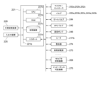
- FIG. 3 is a schematic configuration diagram of the controller 221 included in the substrate processing apparatus 100 preferably used in one aspect of the present disclosure, and is a block diagram showing the control system of the controller 221.
- FIG. FIG. 4(a) is a partially enlarged cross-sectional view of the wafer 200 provided with trenches 301.
- FIG. 4B is an enlarged cross-sectional partial view of the wafer 200 after at least a portion of the inner surface of the trench 301 is modified into the nitride layer 401.
- FIG. FIG. 4C is a partially enlarged cross-sectional view of the wafer 200 in the process of modifying the inner surface of the trench 301 including the nitride layer 401 into the oxide layer 402 .
- FIG. 4(d) is an enlarged cross-sectional partial view of the wafer 200 after the inner surface of the trench 301 including the nitride layer 401 has been modified into the oxide layer 402.
- the drawings used in the following description are all schematic, and the dimensional relationship of each element, the ratio of each element, etc. shown in the drawings do not necessarily match the actual ones. Moreover, the dimensional relationship of each element, the ratio of each element, etc. do not necessarily match between a plurality of drawings.
- the substrate processing apparatus 100 includes a processing furnace 202 that accommodates a wafer 200 as a substrate and performs plasma processing.
- the processing furnace 202 includes a processing container 203 forming a processing chamber 201 .
- the processing container 203 includes a dome-shaped upper container 210 as a first container and a bowl-shaped lower container 211 as a second container.
- a processing chamber 201 is formed by covering the lower container 211 with the upper container 210 .
- the upper container 210 is made of a nonmetallic material such as aluminum oxide (Al 2 O 3 ) or quartz (SiO 2 ), and the lower container 211 is made of aluminum (Al).
- a gate valve 244 as a loading/unloading port is provided on the lower side wall of the lower container 211 .
- the gate valve 244 By opening the gate valve 244 , the wafer 200 can be carried in and out of the processing chamber 201 through the loading/unloading port 245 .
- the gate valve 244 By closing the gate valve 244, the airtightness in the processing chamber 201 can be maintained.
- the processing chamber 201 has a plasma generation space 201a and a substrate processing space 201b communicating with the plasma generation space 201a and in which the wafer 200 is processed.
- the plasma generation space 201a is a space in which plasma is generated, and refers to a space above the lower end of the resonance coil 212 (one-dot chain line in FIG. 1) in the processing chamber 201, for example.
- the substrate processing space 201b is a space in which the substrate is processed with plasma, and is a space below the lower end of the resonance coil 212. As shown in FIG.
- a susceptor 217 as a substrate mounting portion for mounting the wafer 200 is arranged in the center of the bottom side of the processing chamber 201 .
- the susceptor 217 is made of a nonmetallic material such as aluminum nitride (AlN), ceramics, quartz, or the like.
- a heater 217b as a heating mechanism is integrally embedded inside the susceptor 217 .
- the surface of the wafer 200 can be heated to a predetermined degree within the range of 25.degree. C. to 1000.degree.
- the susceptor 217 is electrically insulated from the lower container 211 .
- An impedance adjusting electrode 217c is provided inside the susceptor 217 .
- the impedance adjustment electrode 217c is grounded through an impedance variable mechanism 275 as an impedance adjustment section.
- the impedance variable mechanism 275 includes a coil, a variable capacitor, and the like. By controlling the inductance and resistance of the coil, the capacitance value of the variable capacitor, and the like, the impedance of the impedance adjustment electrode 217c is changed from about 0 ⁇ to the parasitic impedance of the processing chamber 201. It is configured so that it can be changed within a range of values. This makes it possible to control the potential (bias voltage) of the wafer 200 during plasma processing via the impedance adjustment electrode 217c and the susceptor 217.
- a susceptor elevating mechanism 268 for elevating the susceptor is provided below the susceptor 217 .
- the susceptor 217 is provided with a through hole 217a.
- a support pin 266 as a support for supporting the wafer 200 is provided on the bottom surface of the lower container 211 .
- At least three through-holes 217a and support pins 266 are provided at positions facing each other. When the susceptor 217 is lowered by the susceptor lifting mechanism 268, the support pins 266 pass through the through holes 217a without contacting the susceptor 217. As shown in FIG. This allows the wafer 200 to be held from below.
- a gas supply head 236 is provided above the processing chamber 201 , that is, above the upper container 210 .
- the gas supply head 236 includes a cap-shaped lid 233 , a gas inlet 234 , a buffer chamber 237 , an opening 238 , a shielding plate 240 and a gas outlet 239 , and supplies gas into the processing chamber 201 . configured to be supplied.
- the buffer chamber 237 functions as a dispersion space for dispersing the reaction gas introduced from the gas introduction port 234 .
- the gas inlet 234 has a downstream end of a gas supply pipe 232a that supplies a nitrogen-containing gas, a downstream end of a gas supply pipe 232b that supplies an oxygen-containing gas, and a gas supply pipe 232c that supplies an inert gas. connected to merge.
- the gas supply pipe 232a is provided with a nitrogen-containing gas supply source 250a, a mass flow controller (MFC) 252a as a flow control device, and a valve 253a as an on-off valve in this order from the upstream side.
- the gas supply pipe 232b is provided with an oxygen-containing gas supply source 250b, an MFC 252b as a flow control device, and a valve 253b as an on-off valve in this order from the upstream side.
- the gas supply pipe 232c is provided with an inert gas supply source 250c, an MFC 252c as a flow control device, and a valve 253c as an on-off valve in this order from the upstream side.
- a valve 243 a is provided on the downstream side where the gas supply pipe 232 a , the gas supply pipe 232 b , and the gas supply pipe 232 c join together, and is connected to the upstream end of the gas introduction port 234 .
- the MFCs 252a to 252c adjust the flow rates of the respective gases, and the nitrogen-containing gas, the oxygen gas-containing gas, and the inert gas are supplied through the gas supply pipes 232a, 232b, 232c. can be supplied into the processing chamber 201 respectively.
- the nitrogen-containing gas is A supply system is constructed.
- An oxygen-containing gas supply system is mainly composed of the gas supply head 236, the gas supply pipe 232b, the MFC 252b, the valves 253b and 243a.
- An inert gas supply system is mainly composed of the gas supply head 236, the gas supply pipe 232c, the MFC 252c, the valves 253c and 243a.
- a side wall of the lower container 211 is provided with an exhaust port 235 for exhausting the inside of the processing chamber 201 .
- An upstream end of the exhaust pipe 231 is connected to the exhaust port 235 .
- the exhaust pipe 231 is provided with an APC (Auto Pressure Controller) valve 242 and a valve 243b as pressure regulators (pressure regulators) and a vacuum pump 246 as an evacuation device in this order from the upstream side.
- APC Auto Pressure Controller
- the exhaust port 235, the exhaust pipe 231, the APC valve 242, and the valve 243b mainly constitute an exhaust section.
- a vacuum pump 246 may be included in the exhaust.
- a spiral resonance coil 212 is provided on the outer periphery of the processing chamber 201 , that is, on the outside of the side wall of the upper container 210 so as to surround the processing chamber 201 .
- An RF (Radio Frequency) sensor 272 , a high frequency power supply 273 and a frequency matching box 274 (frequency control section) are connected to the resonance coil 212 .
- a shield plate 223 is provided on the outer peripheral side of the resonance coil 212 .
- the high frequency power supply 273 is configured to supply high frequency power to the resonance coil 212 .
- the RF sensor 272 is provided on the output side of the high frequency power supply 273 .
- the RF sensor 272 is configured to monitor information on traveling waves and reflected waves of high-frequency power supplied from the high-frequency power supply 273 .
- the frequency matching device 274 is configured to match the frequency of the high frequency power output from the high frequency power supply 273 based on the reflected wave power information monitored by the RF sensor 272 so as to minimize the reflected wave.
- Both ends of the resonance coil 212 are electrically grounded. One end of the resonance coil 212 is grounded through the movable tap 213 . The other end of resonance coil 212 is grounded through fixed ground 214 . A movable tap 215 is provided between these ends of the resonance coil 212 so that the position at which power is supplied from the high-frequency power supply 273 can be arbitrarily set.
- the resonance coil 212, the RF sensor 272, and the frequency matching box 274 mainly constitute an excitation section (plasma generation section) that excites each of the gases supplied from the nitrogen-containing gas supply system and the oxygen-containing gas supply system. ing.
- the high frequency power source 273 and the shield plate 223 may be included in the excitation section.
- the resonant coil 212 is configured to function as a high frequency inductively coupled plasma (ICP) electrode.
- the winding diameter, winding pitch, number of windings, etc. of the resonance coil 212 are set so as to form a standing wave of a predetermined wavelength and resonate in a full wavelength mode.
- the electrical length of resonance coil 212 that is, the electrode length between the grounds is adjusted to be an integer multiple of the wavelength of the high frequency power supplied from high frequency power supply 273 .
- These configurations, the electric power supplied to the resonance coil 212, the magnetic field intensity generated by the resonance coil 212, and the like are appropriately determined in consideration of the outer shape of the substrate processing apparatus 100, the processing contents, and the like.
- the resonance coil 212 has a coil diameter of 200 to 500 mm and a coil winding number of 2 to 60.
- the high-frequency power supply 273 includes power control means and an amplifier.
- the power control means is configured to output a predetermined high-frequency signal (control signal) to the amplifier based on output conditions related to power and frequency preset through the operation panel.
- the amplifier is configured to output high-frequency power obtained by amplifying the control signal received from the power supply control means toward the resonance coil 212 via the transmission line.
- the frequency matching device 274 receives a voltage signal related to the reflected wave power from the RF sensor 272, and increases or decreases the frequency (oscillation frequency) of the high frequency power output by the high frequency power supply 273 so as to minimize the reflected wave power. corrective control.
- the induced plasma excited in the plasma generation space 201a is of good quality with little capacitive coupling with the inner wall of the processing chamber 201, the susceptor 217, and the like.
- a doughnut-shaped plasma having an extremely low electrical potential is generated in a plan view.
- the controller 221 as a control unit is configured as a computer including a CPU (Central Processing Unit) 221a, a RAM (Random Access Memory) 221b, a storage device 221c, and an I/O port 221d.
- the RAM 221b, storage device 221c, and I/O port 221d are configured to exchange data with the CPU 221a via an internal bus 221e.
- a touch panel, a mouse, a keyboard, an operation terminal, or the like, for example, may be connected to the controller 221 as an input/output device 225 .
- a display for example, may be connected to the controller 221 as a display unit.
- the storage device 221c is composed of, for example, flash memory, HDD (Hard Disk Drive), CD-ROM, and the like.
- a control program for controlling the operation of the substrate processing apparatus 100, a process recipe describing procedures and conditions for substrate processing, and the like are stored in a readable manner.
- a process recipe is a combination of procedures in a substrate processing process, which will be described later, that can be executed by the controller 221 configured as a computer in the substrate processing apparatus 100 to obtain a predetermined result, and functions as a program. do.
- the process recipe, the control program, and the like are collectively referred to simply as a program.
- the RAM 221b is configured as a memory area (work area) in which programs and data read by the CPU 221a are temporarily held.
- the I/O port 221d includes the above MFCs 252a to 252c, valves 253a to 253c, 243a, 243b, gate valve 244, APC valve 242, vacuum pump 246, heater 217b, RF sensor 272, high frequency power supply 273, frequency matching box 274, It is connected to the susceptor lifting mechanism 268, the impedance variable mechanism 275, and the like.
- the CPU 221a is configured to read out and execute a control program from the storage device 221c, and read out a process recipe from the storage device 221c in response to input of an operation command from the input/output device 225 or the like. Then, as shown in FIG. 1, the CPU 221a adjusts the opening of the APC valve 242, opens and closes the valve 243b, and vacuums through the I/O port 221d and the signal line A so as to comply with the content of the read process recipe.
- the pump 246 is started and stopped, the susceptor lifting mechanism 268 is moved up and down through the signal line B, and the heater power adjustment mechanism 276 adjusts the amount of electric power supplied to the heater 217b based on the temperature sensor (temperature adjustment operation) through the signal line C.
- the controller 221 is not limited to being configured as a dedicated computer, and may be configured as a general-purpose computer.
- an external storage device e.g., magnetic tape, magnetic disk such as flexible disk or hard disk, optical disk such as CD or DVD, magneto-optical disk such as MO, semiconductor memory such as USB memory or memory card
- the means for supplying the program to the computer is not limited to supplying via the external storage device 226 .
- the program may be supplied without using the external storage device 226 using communication means such as the Internet or a dedicated line.
- the storage device 221c and the external storage device 226 are configured as computer-readable recording media. Hereinafter, these are collectively referred to simply as recording media.
- the term "recording medium" used in this specification may include only the storage device 221c alone, may include only the external storage device 226 alone, or may include both.
- Substrate Processing Process An example of a substrate processing sequence for processing a wafer 200 as a substrate as one step of a manufacturing process of a semiconductor device using the substrate processing apparatus 100 described above. A sequence example for forming an oxide layer on the inner surface of the recessed structure will be described mainly with reference to FIGS. In the following description, the controller 221 controls the operation of each component of the substrate processing apparatus 100 .
- step a the thickness distribution of the nitride layer on the inner surface is adjusted so that the thickness distribution of the oxide layer on the inner surface, that is, the thickness distribution of the oxide layer formed by performing step b becomes a desired distribution. distribution.
- wafer When the term “wafer” is used in this specification, it may mean the wafer itself, or it may mean a laminate of a wafer and a predetermined layer or film formed on its surface.
- wafer surface may mean the surface of the wafer itself or the surface of a predetermined layer formed on the wafer.
- formation of a predetermined layer on a wafer means that a predetermined layer is formed directly on the surface of the wafer itself, or a layer formed on the wafer, etc. It may mean forming a given layer on top of.
- substrate in this specification is synonymous with the use of the term "wafer”.
- the gate valve 244 is opened, and the wafer 200 to be processed is transferred into the processing chamber 201 by a transfer robot (not shown).
- the wafer 200 loaded into the processing chamber 201 is horizontally supported on support pins 266 projecting from the surface of the susceptor 217 .
- the arm of the transfer robot is withdrawn from the processing chamber 201 and the gate valve 244 is closed.
- the susceptor 217 is raised to a predetermined processing position, and the wafer 200 to be processed is transferred from the support pins 266 onto the susceptor 217 .
- the wafer may be loaded while purging the inside of the processing chamber 201 with an inert gas or the like.
- concave structures such as trenches and holes are formed in advance on the surface of the wafer 200 to be processed.
- FIG. 4A an example in which trenches 301 are formed in advance as concave structures on the surface of a wafer 200 will be described.
- the inner surface of the trench 301 in this aspect shall be comprised by the Si layer which consists of Si simple substance (single-crystal Si, polycrystal Si, or amorphous silicon) as an example.
- the inside of the processing chamber 201 is evacuated by the vacuum pump 246 so as to have a desired processing pressure.
- the pressure inside the processing chamber 201 is measured by a pressure sensor, and the APC valve 242 is feedback-controlled based on this measured pressure information.
- the wafer 200 is heated by the heater 217b so as to reach a desired processing temperature.
- the nitriding processing which will be described later, is started.
- the vacuum pump 246 is kept in operation until wafer unloading, which will be described later, is completed.
- Step a Nitriding
- a nitrogen-containing gas is excited by plasma and supplied to the wafer 200 in the processing chamber 201 .
- the valve 253a is opened to allow the nitrogen-containing gas to flow into the gas supply pipe 232a.
- the nitrogen-containing gas is adjusted in flow rate by the MFC 252 a, supplied into the processing chamber 201 through the buffer chamber 237 , and exhausted through the exhaust port 235 .
- the nitrogen-containing gas is supplied to the wafer 200 from above the wafer 200 (nitrogen-containing gas supply).
- the inert gas may be supplied into the processing chamber 201 through the buffer chamber 237 by opening the valve 243c.
- Nitriding species include at least one of excited state N atoms (N * ) and ionized N atoms.
- * means a radical.
- the nitriding species when a gas containing hydrogen (H) is used as the nitrogen-containing gas, the nitriding species further include at least one of an excited NH group (NH * ) and ions containing N and H. included. Furthermore, in this case, reactive species such as excited H atoms (H * ) and ionized H atoms may also be generated. These reactive species can also be considered as part of the nitriding species.
- the processing conditions in this step are as follows: Treatment temperature: room temperature to 1000°C, preferably 650 to 900°C Treatment pressure: 1 to 100 Pa, preferably 3 to 10 Pa Nitrogen-containing gas supply flow rate: 0.1 to 10 slm, preferably 0.15 to 0.5 slm Nitrogen-containing gas supply time: 10 to 600 seconds, preferably 20 to 50 seconds Inert gas supply flow rate: 0 to 10 slm RF power: 100-5000W, preferably 500-3500W RF frequency: 800kHz-50MHz are exemplified.
- the expression of a numerical range such as "650 to 900° C.” in this specification means that the lower limit and upper limit are included in the range. Therefore, for example, “650 to 900°C” means “650°C to 900°C”. The same applies to other numerical ranges.
- the processing temperature in this specification means the temperature of the wafer 200 or the temperature inside the processing chamber 201
- the processing pressure means the pressure inside the processing chamber 201 .
- the gas supply flow rate: 0 slm means a case where the gas is not supplied.
- Nitriding species are supplied to the inner surface of the trench 301 by plasma-exciting a nitrogen-containing gas and supplying it to the wafer 200 under the processing conditions described above.
- the inner surface of the trench 301 is nitrided by the supplied nitriding species, and at least part of the inner surface is modified into a nitride layer 401 (see FIG. 4B).
- the thickness distribution of the nitride layer 401 can be such that the thickness gradually decreases from the opening 301a of the trench 301 toward the bottom 301b (see FIG. 4(b)).
- the inner surface near the opening 301a of the trench 301 may be modified with the nitride layer 401, and the inner surface near the bottom 301b may not be modified with the nitride layer 401 (FIG. 4(b)).
- the reason why the thickness distribution of the nitride layer 401 can be such a distribution is that the nitriding species supplied to the inner surface of the trench 301 preferentially reacts with the inner surface near the opening 301a and is consumed.
- the supply amount of the nitriding species gradually decreases from the opening 301a toward the bottom 301b. Further, the nitriding species supplied to the inner surface of the trench 301 are deactivated while moving from the vicinity of the opening 301a to the bottom 301b, and the supply amount of the nitriding species gradually increases from the opening 301a toward the bottom 301b. This is also to reduce the
- the thickness of the nitride layer 401 at the opening 301a of the trench 301 can be set to 1 to 3 nm, for example.
- the thickness of the nitride layer 401 has the effect of controlling (suppressing) the oxidation rate in step b, regardless of its size (thinness), as will be described later.
- the processing pressure is set to a relatively high pressure in order to ensure that the thickness distribution of the nitride layer 401 has the above distribution.
- the processing pressure at which the thickness distribution of the nitride layer 401 formed by performing step a becomes uniform over the entire inner surface of the trench 301 is defined as the “first pressure”.
- the processing pressure is set to a second pressure higher than the first pressure.
- the valve 253a is closed to stop the supply of nitrogen-containing gas into the processing chamber 201 and the supply of RF power to the resonance coil 212. Then, the inside of the processing chamber 201 is evacuated, and gas and the like remaining in the processing chamber 201 are removed from the inside of the processing chamber 201 . At this time, the valve 253 c is opened to supply inert gas into the processing chamber 201 .
- the inert gas acts as a purge gas, thereby purging the inside of the processing chamber 201 (purge).
- nitrogen-containing gas examples include nitrogen (N 2 ) gas, nitriding gas such as ammonia (NH 3 ) gas, diazene (N 2 H 2 ) gas, hydrazine (N 2 H 4 ) gas, and N 3 H 8 gas.
- a hydrogen-based gas can be used. One or more of these can be used as the nitrogen-containing gas.
- a mixed gas of a nitrogen-containing gas and a hydrogen-containing gas such as a mixed gas of N 2 gas and hydrogen (H 2 ) gas, can be used.
- the nitridation rate for a simple film such as a Si film is higher than that for a simple film such as a Si film when a gas containing hydrogen is used as the nitrogen-containing gas. It tends to be faster than speed. Therefore, if a natural oxide film having uneven thickness is formed on the inner surface of the trench 301 , the natural oxide film may affect the surface of the wafer 200 . It may be difficult to control the thickness distribution of the nitride layer 401 .
- the nitrogen-containing gas by using a gas that does not contain H (for example, N 2 gas) as the nitrogen-containing gas, the influence of the natural oxide film can be suppressed, and the thickness of the nitride layer 401 formed on the surface of the wafer 200 can be reduced. It is possible to improve the controllability of the distribution, which is preferable.
- a gas that does not contain H for example, N 2 gas
- the inert gas for example, N2 gas, rare gas such as argon (Ar) gas, helium (He) gas, neon (Ne) gas, and xenon (Xe) gas can be used.
- Ar argon
- He helium
- Ne neon
- Xe xenon
- Step b oxidation treatment
- the plasma-excited oxygen-containing gas is supplied to the wafer 200 in the processing chamber 201 .
- valve 253b is opened to allow the oxygen-containing gas to flow into the gas supply pipe 232b.
- the flow rate of the oxygen-containing gas is adjusted by the MFC 252 b , supplied into the processing chamber 201 through the buffer chamber 237 , and exhausted from the exhaust port 235 .
- an oxygen-containing gas is supplied to the wafers 200 from above the wafers 200 (oxygen-containing gas supply).
- the inert gas may be supplied into the processing chamber 201 through the buffer chamber 237 by opening the valve 243c.
- the excitation of the inductive plasma activates the oxygen-containing gas and produces oxidizing species.
- the oxidizing species includes at least one of excited state O atoms (O * ) and ionized O atoms.
- the oxygen-containing gas the oxidizing species further includes at least one of excited OH groups (OH * ) and ions containing O and H.
- reactive species such as excited H atoms (H * ) and ionized H atoms may also be generated. These reactive species can also be considered as part of the oxidizing species.
- the processing conditions in this step are as follows: Treatment temperature: room temperature to 1000°C, preferably 650 to 900°C Treatment pressure: 1 to 1000 Pa, preferably 100 to 200 Pa Oxygen-containing gas supply flow rate: 0.1 to 10 slm, preferably 0.2 to 0.5 slm Oxygen-containing gas supply time: 10 to 400 seconds, preferably 20 to 50 seconds.
- Other processing conditions are the same as the processing conditions for supplying the nitrogen-containing gas in step a.
- Oxidizing species are supplied to the inner surface of the trench 301 by supplying the plasma-excited oxygen-containing gas to the wafer 200 under the above-described processing conditions.
- the supplied oxidizing species oxidizes the inner surface of the trench 301 including the nitride layer 401 and reforms it into an oxide layer 402 (see FIG. 4C).
- the nitride layer 401 can be reformed into the oxide layer 402 over the entire thickness direction of the nitride layer 401 .
- the nitride layer 401 and a predetermined region (N diffuses) which is a region deeper than the nitride layer 401 in the thickness direction of the nitride layer 401 and is not modified by the nitride layer 401.
- the underlying regions that are not exposed) and can each be modified to an oxide layer 402 . That is, the inner surface modified to the nitride layer 401 by performing step a and the inner surface not modified to the nitride layer 401 by performing step a are each modified to the oxide layer 402. be able to
- the thickness distribution of the oxide layer 402 gradually increases from the opening 301a of the trench 301 toward the bottom 301b. See FIG. 4(d)).
- the thickness distribution of the nitride layer 401 formed in step a is such that the thickness gradually decreases from the opening 301a of the trench 301 toward the bottom 301b. Further, preferably, the inner surface of the trench 301 near the bottom 301b is not modified by the nitride layer 401 .
- the oxidation rate of the opening 301 a of the trench 301 is lower than the oxidation rate of the bottom 301 b of the trench 301 .
- the oxidation rate on the inner surface of the trench 301 is, for example, lowest at the opening 301a of the trench 301 and gradually increases from the opening 301a toward the bottom 301b.
- the thickness distribution of the oxide layer 402 is such that the thickness gradually increases from the opening 301 a of the trench 301 toward the bottom 301 b , and the thickness of the oxide layer 402 increases from the bottom of the trench 301 .
- 301b can be the thickest. That is, in step a, the thickness distribution of the oxide layer 402 in step b gradually increases from the opening 301a of the trench 301 toward the bottom 301b, and/or the thickness of the oxide layer 402 is The thickness distribution of the nitride layer 401 can be adjusted such that the thickness distribution is thickest at the bottom 301 b of the trench 301 . In this case, the thickness of the oxide layer 402 at the bottom 301b of the trench 301 can be, for example, 5 to 7 nm.
- step a it is possible to make the thickness distribution of the oxide layer 402 formed in step b uniform over the entire inner surface of the trench 301 . That is, in step a, the thickness distribution of the nitride layer 401 is adjusted so that the thickness distribution of the oxide layer 402 formed in step b is uniform over the entire inner surface of the trench 301 . can be done.
- valve 253b is closed to stop the supply of oxygen-containing gas into the processing chamber 201 and the supply of RF power to the resonance coil 212 .
- oxygen-containing gas examples include oxygen (O 2 ) gas, ozone (O 3 ) gas, O 2 gas + hydrogen (H 2 ) gas, water vapor (H 2 O), and hydrogen peroxide (H 2 O 2 ) gas. etc. can be used. One or more of these can be used as the oxygen-containing gas.
- the oxygen-containing gas should be a gas containing hydrogen (H) in addition to oxygen (O). 2 gas + H 2 gas is preferably used.
- H hydrogen
- 2 gas + H 2 gas is preferably used.
- step b After purge, return to atmospheric pressure, the inside of the processing chamber 201 is evacuated to remove the gas and the like remaining in the processing chamber 201 from the inside of the processing chamber 201 . Then, gaseous substances remaining in the processing chamber 201 are removed from the processing chamber 201 (after-purge) by the same processing procedure and processing conditions as the purge described above. After that, the atmosphere in the processing chamber 201 is replaced with the purge gas, and the pressure in the processing chamber 201 is restored to normal pressure (return to atmospheric pressure).
- the susceptor 217 is lowered to a predetermined transfer position, and the wafer 200 is transferred from the susceptor 217 onto the support pins 266 .
- the gate valve 244 is opened, and the processed wafer 200 is carried out of the processing chamber 201 using a transfer robot (not shown). With the above, the substrate processing process according to this aspect is finished.
- step a before performing step b (a) Performing step a before performing step b, and setting the thickness distribution of the nitride layer 401 formed by performing step a to a predetermined distribution, thereby forming the nitride layer 401 formed by performing step b. It is possible to obtain a desired thickness distribution of the oxide layer 402 .
- step a the inner surface (especially the sidewall surface) near the opening 301a of the trench 301 is modified to the nitride layer 401, and the inner surface near the bottom 301b of the trench 301 is not modified to the nitride layer 401.
- the thickness distribution of the oxide layer 402 formed by performing step b can be such that the thickness near the bottom 301b is greater than the thickness near the opening 301a.
- step a the inner surface (especially the side wall surface) of the trench 301 is reformed into the nitride layer 401 so that the thickness distribution becomes gradually thinner from the opening 301a toward the bottom 301b, The inner surface of the trench 301 near the bottom 301b should not be reformed into the nitride layer 401.
- the thickness distribution of the oxide layer 402 formed by performing step b gradually increases from the opening 301a of the trench 301 toward the bottom 301b, and becomes the thickest at the bottom 301b. becomes possible.
- step a while the entire inner surface of the trench 301 (surfaces including the side wall surfaces and the bottom surface) is modified into the nitride layer 401, the thickness distribution of the nitride layer 401 is changed to the opening 301a of the trench 301. It has a predetermined distribution such that it gradually becomes thinner from the bottom 301b. As a result, the thickness distribution of the oxide layer 402 formed by performing step b can be made uniform over the entire inner surface of the trench 301 .
- step a the nitrogen-containing gas is excited by applying energy from plasma, heat, light, or the like to generate nitriding seeds, and the nitriding seeds are supplied to the wafer 200 to form the nitride layer 401. It can be done efficiently. In addition, by utilizing the fact that the generated nitriding species have a short life, the controllability of the thickness distribution of the nitrided layer 401 formed by performing step a is enhanced, and in turn, by performing step b. It is possible to improve the controllability of the thickness distribution of the oxide layer 402 to be formed.
- step b energy is applied by plasma, heat, light, or the like to excite the oxygen-containing gas to generate oxidizing species. It can be done efficiently.
- steps a and b the nitride layer 401 and the oxide layer 402 can be formed under relatively low temperature conditions by exciting the nitrogen-containing gas and the oxygen-containing gas with plasma, respectively. Become. These allow the thermal history of the wafer 200 to be reduced.
- step a by using a gas that does not contain H as the nitrogen-containing gas, it is possible to suppress the influence of a native oxide film having a non-uniform thickness formed on the inner surface of the trench 301. It is possible to improve the controllability of the thickness distribution of the nitride layer 401 formed on the inner surface of 301 and, in turn, the controllability of the thickness distribution of the oxide layer 402 .
- step b by using a gas containing H as the oxygen-containing gas, it is possible to increase the oxidizing power of the oxygen-containing gas and improve the efficiency of the oxidation treatment.
- the ratio of the H component (the number of H atoms) to the O component (the number of O atoms) contained in the oxygen-containing gas Si alone (non-nitriding) with respect to the oxidation treatment to SiN (nitride) can increase the selectivity of the oxidation treatment to the material) (the above R Si /R SiN can be increased). Therefore, for example, if the thickness of the nitride layer 401 formed on the bottom 301b of the trench 301 in step a is small, or if the nitride layer 401 is formed so that the nitride layer 401 is not formed, the ratio of the H component should be increased.
- the thickness of the oxide layer 402 formed on the bottom portion 301b can be further selectively increased.
- the nitride layer 401 is formed so as to have a thickness distribution that gradually decreases from the opening 301a toward the bottom 301b in step a
- increasing the ratio of the H component results in
- the thickness gradient of the oxide layer 402, which increases in thickness from the opening 301a toward the bottom 301b, can be adjusted to further increase.
- the thickness of the oxide layer 402 is further increased. It is possible to control the distribution of That is, by adjusting the ratio of the H component, it is possible to improve the controllability of the thickness distribution of the oxide layer 402 formed by performing step b.
- step b substantially no N remains in the oxide layer 402 by modifying the nitride layer 401 into the oxide layer 402 throughout the thickness direction of the nitride layer 401. becomes possible.
- step b of the inner surface of the trench 301, the nitride layer 401 and a predetermined region which is deeper than the nitride layer 401 in the thickness direction of the nitride layer 401 and has not been modified to the nitride layer 401.
- modifying each of (underlying region where N is not diffused) into the oxide layer 402 it becomes possible to prevent N from remaining in the oxide layer 402 more reliably.
- the substrate processing sequence in this aspect can be modified as in the following modifications. These modifications can be combined arbitrarily. Unless otherwise specified, the processing procedures and processing conditions in each step of each modification can be the same as the processing procedures and processing conditions in each step of the substrate processing sequence described above.
- step a the treatment pressure is set to a relatively low pressure to reduce the amount of nitriding species generated, and to control the thickness distribution of the nitride layer 401 and, in turn, the thickness distribution of the oxide layer 402. good.
- the processing pressure is set to a third pressure that is lower than the "first pressure" referred to in the description of the above aspects.
- the same effect as the above-described mode can be obtained.
- the amount of nitriding species supplied to the wafer 200 is reduced, most of the nitriding species is consumed near the opening 301a of the trench 301, and the nitriding species is prevented from reaching the bottom 301b. It becomes possible. As a result, the thickness distribution of the nitride layer 401 can be easily made such that the thickness gradually decreases from the opening 301a of the trench 301 toward the bottom 301b.
- the RF power may be relatively low to reduce the amount of nitriding species produced and to control the thickness distribution of the nitride layer 401 and thus the thickness distribution of the oxide layer 402 .
- the value of the RF power such that the thickness distribution of the nitride layer 401 formed by performing the step a becomes a uniform thickness distribution over the entire inner surface of the trench 301 is set as the "first power value.
- the RF power value is set to a second power value lower than the first power value.
- the same effect as the above-described mode can be obtained.
- the amount of nitriding species supplied to the wafer 200 is reduced, most of the nitriding species is consumed near the opening 301a of the trench 301, and the nitriding species is prevented from reaching the bottom 301b. It becomes possible. As a result, the thickness distribution of the nitride layer 401 can be easily made such that the thickness gradually decreases from the opening 301a of the trench 301 toward the bottom 301b.
- step a the amount of nitriding species supplied to the wafer 200 is reduced by relatively shortening the supply time of the nitrogen-containing gas, thereby reducing the thickness distribution of the nitride layer 401 and, in turn, the thickness distribution of the oxide layer 402. may be controlled.
- the supply time during which the thickness distribution of the nitride layer 401 formed by performing step a becomes a uniform thickness distribution over the entire inner surface of the trench 301 is referred to as the “first supply time”.
- WHEREIN He is trying to make supply time into the 2nd supply time shorter than this 1st supply time.
- the same effect as the above-described mode can be obtained.
- the amount of nitriding species supplied to the wafer 200 is reduced, most of the nitriding species is consumed near the opening 301a of the trench 301, and the nitriding species is prevented from reaching the bottom 301b. It becomes possible. As a result, the thickness distribution of the nitride layer 401 can be easily made such that the thickness gradually decreases from the opening 301a of the trench 301 toward the bottom 301b.
- step a ion components such as ionized N atoms are used as the nitriding species to be supplied to the wafer 200 so as to control the thickness distribution of the nitride layer 401 and, in turn, the thickness distribution of the oxide layer 402. good too.
- the impedance variable mechanism 275 is adjusted to control the potential (bias voltage) of the wafer 200 in step a through the impedance adjustment electrode 217 c and the susceptor 217 .
- the distribution of nitriding by the ion component of the nitriding species drawn into the trench 301 is adjusted so that the thickness distribution of the nitrided layer 401 becomes a desired distribution.
- ion components such as ionized N atoms have a short mean free path even if the processing pressure is lowered, so they tend to react biasedly toward the inner surface near the opening 301a of the trench 301 .
- the thickness distribution of the nitride layer 401 can be easily made such that the thickness gradually decreases from the opening 301a of the trench 301 toward the bottom 301b.
- the thickness distribution of the nitride layer 401 and thus the thickness distribution of the oxide layer 402 may be controlled by relatively increasing the flow rate of the nitrogen-containing gas.
- the flow velocity at which the thickness distribution of the nitride layer 401 formed by performing the step a becomes a uniform thickness distribution over the entire inner surface of the trench 301 is defined as the “first flow velocity”.
- the flow velocity is set to a second flow velocity that is greater than the first flow velocity.
- the flow velocity of the nitrogen-containing gas is adjusted, for example, by controlling the supply flow rate of the nitrogen-containing gas into the processing chamber 201 .
- the same effect as the above-described mode can be obtained.
- the flow velocity of the nitriding species in the vicinity of the bottom portion 301b is relatively decreased with respect to the flow velocity of the nitriding species in the vicinity of the opening portion 301a. It becomes possible to preferentially nitride the inner surface near the opening 301a. As a result, the thickness distribution of the nitride layer 401 can be easily made such that the thickness gradually decreases from the opening 301a of the trench 301 toward the bottom 301b.
- the nitrogen-containing gas and the oxygen-containing gas may be excited by heat or light. Also in this case, the same effect as the above-described mode can be obtained. Also, plasma damage to the wafer 200 or the like can be avoided.
- the trench 301 was taken as an example of the recessed structure, but the present disclosure is not limited to this.
- holes may be formed as concave structures on the surface of the wafer 200 .
- the structure of the recess may be formed so that the width becomes wider (so that the distance between the opposing inner surfaces gradually increases) from the opening 301a toward the bottom 301b. Further, the width may be narrowed from the opening 301a toward the bottom 301b (so that the distance between the opposing inner surfaces gradually decreases). Also in these cases, the same effects as those of the above embodiments can be obtained.
- a wafer 200 in which trenches 301 having an aspect ratio of 10 or more or 20 or more are formed can be used. According to the present disclosure, even when using a wafer 200 having such a high aspect ratio, effects similar to those of the above aspect can be obtained.
- the inner surface of the trench 301 may be composed of Si-containing substances (Si compounds) such as silicon carbide (SiC) and silicon germanium (SiGe).
- the inner surface of trench 301 may be made of a metal containing aluminum (Al), titanium (Ti), hafnium (Hf), or zirconium (Zr), or a compound thereof.
- the inner surface of trench 301 is preferably other than these oxides and nitrides.
- step a an example in which the nitriding process (step a) and the oxidation process (step b) are continuously performed in a single processing chamber (that is, the processing chamber 201) has been described, but the present disclosure is not limited to this.
- the substrate is unloaded from the processing chamber in which the nitriding has been performed to a transfer chamber that is not open to the atmosphere. After that, the substrate may be carried into another processing chamber and subjected to oxidation processing (step b).
Landscapes
- Physics & Mathematics (AREA)
- Engineering & Computer Science (AREA)
- Plasma & Fusion (AREA)
- Chemical & Material Sciences (AREA)
- Analytical Chemistry (AREA)
- Formation Of Insulating Films (AREA)
Abstract
Description
(a)基板上に形成された凹状構造の内表面を窒化し、前記内表面の少なくとも一部を窒化層に改質する工程と、
(b)前記窒化層を含む前記内表面を酸化し、前記内表面を酸化層に改質する工程と、
を有し、
(a)では、前記内表面における前記窒化層の厚さの分布を、前記内表面における前記酸化層の厚さの分布が所望の分布になるような分布とする技術が提供される。
以下、本開示の一態様について、主に、図1~図3、図4(a)~図4(d)を参照しつつ説明する。なお、以下の説明において用いられる図面は、いずれも模式的なものであり、図面に示される、各要素の寸法の関係、各要素の比率等は、現実のものとは必ずしも一致していない。また、複数の図面の相互間においても、各要素の寸法の関係、各要素の比率等は必ずしも一致していない。
図1に示すように、基板処理装置100は、基板としてのウエハ200を収容してプラズマ処理する処理炉202を備えている。処理炉202は、処理室201を構成する処理容器203を備えている。処理容器203は、第1の容器であるドーム型の上側容器210と、第2の容器である碗型の下側容器211とを備えている。上側容器210が下側容器211の上に被さることにより、処理室201が形成されている。上側容器210は、例えば酸化アルミニウム(Al2O3)または石英(SiO2)等の非金属材料により構成されており、下側容器211は、例えばアルミニウム(Al)により構成されている。
上述の基板処理装置100を用い、半導体装置の製造工程の一工程として、基板としてのウエハ200を処理する基板処理シーケンス例、具体的には、ウエハ200の表面に形成された凹状構造の内表面に酸化層を形成するシーケンス例について、主に図4(a)、図4(b)、図4(c)、図4(d)を用いて説明する。以下の説明において、基板処理装置100を構成する各部の動作はコントローラ221により制御される。
ウエハ200上に形成された凹状構造の内表面を窒化し、内表面の少なくとも一部を窒化層に改質するステップaと、
窒化層を含む内表面を酸化し、内表面を酸化層に改質するステップbと、
を実施する。
サセプタ217を所定の搬送位置まで降下させた状態で、ゲートバルブ244を開き、処理対象のウエハ200を、搬送ロボット(図示せず)により処理室201内へ搬入する。処理室201内へ搬入されたウエハ200は、サセプタ217の表面から突出した支持ピン266上に水平姿勢で支持される。処理室201内へのウエハ200の搬入が完了した後、処理室201内から搬送ロボットのアーム部を退去させ、ゲートバルブ244を閉じる。その後、サセプタ217を所定の処理位置まで上昇させ、処理対象のウエハ200を、支持ピン266上からサセプタ217上へと移載させる。なお、ウエハ搬入は、処理室201内を不活性ガス等でパージしながら行ってもよい。
続いて、処理室201内が所望の処理圧力となるように、真空ポンプ246によって真空排気される。処理室201内の圧力は圧力センサで測定され、この測定された圧力情報に基づきAPCバルブ242がフィードバック制御される。また、ウエハ200が所望の処理温度となるように、ヒータ217bによって加熱される。処理室201内が所望の処理圧力となり、また、ウエハ200の温度が所望の処理温度に到達して安定したら、後述する窒化処理を開始する。真空ポンプ246は、後述するウエハ搬出が終了するまで作動させておく。
ステップaでは、処理室201内のウエハ200に対して窒素含有ガスをプラズマで励起させて供給する。
処理温度:室温~1000℃、好ましくは650~900℃
処理圧力:1~100Pa、好ましくは3~10Pa
窒素含有ガス供給流量:0.1~10slm、好ましくは0.15~0.5slm
窒素含有ガス供給時間:10~600秒、好ましくは20~50秒
不活性ガス供給流量:0~10slm
RF電力:100~5000W、好ましくは500~3500W
RF周波数:800kHz~50MHz
が例示される。
ステップbでは、処理室201内のウエハ200に対して酸素含有ガスをプラズマで励起させて供給する。
処理温度:室温~1000℃、好ましくは650~900℃
処理圧力:1~1000Pa、好ましくは100~200Pa
酸素含有ガス供給流量:0.1~10slm、好ましくは0.2~0.5slm
酸素含有ガス供給時間:10~400秒、好ましくは20~50秒
が例示される。他の処理条件は、ステップaにて窒素含有ガスを供給する際における処理条件と同様にする。
ステップbが終了したら、処理室201内を真空排気し、処理室201内に残留するガス等を処理室201内から排除する。そして、上述のパージと同様の処理手順、処理条件により、処理室201内に残留するガス状物質等を処理室201内から排除する(アフターパージ)。その後、処理室201内の雰囲気がパージガスに置換され、処理室201内の圧力が常圧に復帰される(大気圧復帰)。
続いて、サセプタ217を所定の搬送位置まで下降させ、ウエハ200を、サセプタ217上から支持ピン266上へと移載させる。その後、ゲートバルブ244を開き、図示しない搬送ロボットを用い、処理後のウエハ200を処理室201外へ搬出する。以上により、本態様に係る基板処理工程を終了する。
本態様によれば、以下に示す1つ又は複数の効果が得られる。
本態様における基板処理シーケンスは、以下に示す変形例のように変更することができる。これらの変形例は、任意に組み合わせることができる。特に説明がない限り、各変形例の各ステップにおける処理手順、処理条件は、上述の基板処理シーケンスの各ステップにおける処理手順、処理条件と同様とすることができる。
ステップaでは、処理圧力を比較的低い圧力とすることにより、生成される窒化種の量を減らし、窒化層401の厚さ分布、ひいては、酸化層402の厚さ分布を制御するようにしてもよい。具体的には、処理圧力を、上述の態様における説明で言及した「第1圧力」よりも低い第3圧力とするようにしている。
ステップaでは、RF電力を比較的低くすることにより、生成される窒化種の量を減らし、窒化層401の厚さ分布、ひいては、酸化層402の厚さ分布を制御するようにしてもよい。具体的には、ステップaを行うことで形成される窒化層401の厚さ分布がトレンチ301の内表面の全面おいて均一な厚さ分布となるようなRF電力の値を「第1電力値」とする場合において、RF電力の値を、この第1電力値よりも低い第2電力値とするようにしている。
ステップaでは、窒素含有ガスの供給時間を比較的短くすることにより、ウエハ200に対して供給される窒化種の量を減らし、窒化層401の厚さ分布、ひいては、酸化層402の厚さ分布を制御するようにしてもよい。具体的には、ステップaを行うことで形成される窒化層401の厚さ分布がトレンチ301の内表面の全面おいて均一な厚さ分布となるような供給時間を「第1供給時間」とする場合において、供給時間を、この第1供給時間よりも短い第2供給時間とするようにしている。
ステップaでは、ウエハ200に供給する窒化種として、イオン化されたN原子などのイオン成分を用いることにより、窒化層401の厚さ分布、ひいては、酸化層402の厚さ分布を制御するようにしてもよい。具体的には、インピーダンス可変機構275を調整し、インピーダンス調整電極217c及びサセプタ217を介して、ステップaにおけるウエハ200の電位(バイアス電圧)を制御する。これにより、窒化層401の厚さ分布が所望の分布となるように、トレンチ301内に引き込まれる窒化種のイオン成分による窒化の分布を調整する。
ステップaでは、窒素含有ガスの流速を比較的大きくすることにより、窒化層401の厚さ分布、ひいては、酸化層402の厚さ分布を制御するようにしてもよい。具体的には、ステップaを行うことで形成される窒化層401の厚さ分布がトレンチ301の内表面の全面おいて均一な厚さ分布となるような流速を「第1流速」とする場合において、流速を、この第1流速よりも大きい第2流速とするようにしている。窒素含有ガスの流速は、例えば、処理室201内への窒素含有ガスの供給流量を制御することにより調整する。
以上、本開示の態様を具体的に説明した。しかしながら、本開示は上述の態様に限定されるものではなく、その要旨を逸脱しない範囲で種々変更可能である。
301 トレンチ(凹状構造)
401 窒化層
402 酸化層
Claims (20)
- (a)基板上に形成された凹状構造の内表面を窒化し、前記内表面の少なくとも一部を窒化層に改質する工程と、
(b)前記窒化層を含む前記内表面を酸化し、前記内表面を酸化層に改質する工程と、
を有し、
(a)では、前記内表面における前記窒化層の厚さの分布を、前記内表面における前記酸化層の厚さの分布が所望の分布になるような分布とする半導体装置の製造方法。 - (a)では、窒素含有ガスを励起して窒化種を生成し、前記窒化種を前記基板に供給する請求項1に記載の半導体装置の製造方法。
- (a)では、プラズマまたは熱により前記窒素含有ガスを励起する請求項2に記載の半導体装置の製造方法。
- 前記窒素含有ガスは、水素を非含有とするガスである請求項2または3に記載の半導体装置の製造方法。
- (a)では、前記窒化層の厚さの分布を、前記凹状構造の開口部から底部に向かうにしたがって徐々に薄くなるような分布とする請求項1~4のいずれか1項に記載の半導体装置の製造方法。
- (a)では、前記内表面の全面を前記窒化層に改質する請求項1~5のいずれか1項に記載の半導体装置の製造方法。
- (a)では、前記凹状構造の開口部付近の前記内表面を前記窒化層に改質し、前記凹状構造の底部付近の前記内表面を前記窒化層に改質しない請求項1~5のいずれか1項に記載の半導体装置の製造方法。
- (a)において窒化される前記内表面は、シリコンを含有する請求項1~7のいずれか1項に記載の半導体装置の製造方法。
- (b)では、酸素含有ガスを励起して酸化種を生成し、前記酸化種を前記基板に供給する請求項1~8のいずれか1項に記載の半導体装置の製造方法。
- (b)では、プラズマまたは熱により前記酸素含有ガスを励起する請求項9に記載の半導体装置の製造方法。
- 前記酸素含有ガスは、水素を含有するガスである請求項9または10に記載の半導体装置の製造方法。
- (b)では、前記酸素含有ガスに含まれる酸素に対する水素の比率を調整することにより、前記酸化層の厚さの分布を制御する請求項11に記載の半導体装置の製造方法。
- (b)では、前記窒化層の厚さ方向の全体に亘って、前記窒化層を前記酸化層に改質する請求項1~12のいずれか1項に記載の半導体装置の製造方法。
- (b)では、前記酸化層の厚さの分布を、前記凹状構造の開口部から底部に向かうにしたがって徐々に厚くなり、前記底部において最も厚くなるような分布とする請求項1~13のいずれか1項に記載の半導体装置の製造方法。
- (a)では、前記窒化層の厚さの分布を、前記酸化層の厚さの分布が、前記凹状構造の開口部から底部に向かうにしたがって徐々に厚くなり、前記底部において最も厚くなる分布になるような分布とする請求項14に記載の半導体装置の製造方法。
- (b)では、前記酸化層の厚さの分布を、前記内表面の全面おいて均一となるような分布とする請求項1~13のいずれか1項に記載の半導体装置の製造方法。
- (a)では、前記窒化層の厚さの分布を、前記酸化層の厚さの分布が、前記内表面の全面おいて均一となる分布になるような分布とする請求項16に記載の半導体装置の製造方法。
- (a)基板上に形成された凹状構造の内表面を窒化し、前記内表面の少なくとも一部を窒化層に改質する工程と、
(b)前記窒化層を含む前記内表面を酸化し、前記内表面を酸化層に改質する工程と、
を有し、
(a)では、前記内表面における前記窒化層の厚さの分布を、前記内表面における前記酸化層の厚さの分布が所望の分布になるような分布とする基板処理方法。 - 基板を収容する処理室と、
前記処理室内に窒素含有ガスを供給する窒素含有ガス供給系と、
前記処理室内に酸素含有ガスを供給する酸素含有ガス供給系と、
前記窒素含有ガス供給系および前記酸素含有ガス供給系から供給されるガスを励起する励起部と、
前記処理室内で、(a)前記窒素含有ガスを励起することで生成した窒化種を表面に凹状構造が形成された基板に対して供給し、前記凹状構造の内表面を窒化し、前記内表面の少なくとも一部を窒化層に改質する処理と、(b)前記酸素含有ガスを励起することで生成した酸化種を前記基板に対して供給し、前記窒化層を含む前記内表面を酸化し、前記内表面を酸化層に改質する処理と、を行わせ、(a)では、前記内表面における前記窒化層の厚さの分布を、前記内表面における前記酸化層の厚さの分布が所望の分布になるような分布とするように、前記窒素含有ガス供給系、前記酸素含有ガス供給系、および前記励起部を制御することが可能なように構成される制御部と、
を有する基板処理装置。 - 基板処理装置の処理室内において、
(a)基板上に形成された凹状構造の内表面を窒化し、前記内表面の少なくとも一部を窒化層に改質する工程と、
(b)前記窒化層を含む前記内表面を酸化し、前記内表面を酸化層に改質する工程と、
(a)において、前記内表面における前記窒化層の厚さの分布を、前記内表面における前記酸化層の厚さの分布が所望の分布になるような分布とする手順と、
をコンピュータによって前記基板処理装置に実行させるプログラム。
Priority Applications (7)
| Application Number | Priority Date | Filing Date | Title |
|---|---|---|---|
| CN202180101667.9A CN117836917A (zh) | 2021-09-29 | 2021-09-29 | 半导体器件的制造方法、衬底处理方法、衬底处理装置及程序 |
| PCT/JP2021/035835 WO2023053262A1 (ja) | 2021-09-29 | 2021-09-29 | 半導体装置の製造方法、基板処理方法、基板処理装置、およびプログラム |
| JP2023550840A JP7777141B2 (ja) | 2021-09-29 | 2021-09-29 | 基板処理方法、半導体装置の製造方法、基板処理装置、およびプログラム |
| KR1020247005907A KR20240042456A (ko) | 2021-09-29 | 2021-09-29 | 기판 처리 방법, 반도체 장치의 제조 방법, 기판 처리 장치 및 프로그램 |
| TW113124663A TW202441626A (zh) | 2021-09-29 | 2022-07-18 | 半導體裝置的製造方法、基板處理方法、基板處理裝置、及程式 |
| TW111126812A TWI850709B (zh) | 2021-09-29 | 2022-07-18 | 半導體裝置的製造方法、基板處理方法、基板處理裝置、及程式 |
| US18/583,444 US20240194476A1 (en) | 2021-09-29 | 2024-02-21 | Method of processing substrate, method of manufacturing semiconductor device, substrate processing apparatus, and recording medium |
Applications Claiming Priority (1)
| Application Number | Priority Date | Filing Date | Title |
|---|---|---|---|
| PCT/JP2021/035835 WO2023053262A1 (ja) | 2021-09-29 | 2021-09-29 | 半導体装置の製造方法、基板処理方法、基板処理装置、およびプログラム |
Related Child Applications (1)
| Application Number | Title | Priority Date | Filing Date |
|---|---|---|---|
| US18/583,444 Continuation US20240194476A1 (en) | 2021-09-29 | 2024-02-21 | Method of processing substrate, method of manufacturing semiconductor device, substrate processing apparatus, and recording medium |
Publications (1)
| Publication Number | Publication Date |
|---|---|
| WO2023053262A1 true WO2023053262A1 (ja) | 2023-04-06 |
Family
ID=85781570
Family Applications (1)
| Application Number | Title | Priority Date | Filing Date |
|---|---|---|---|
| PCT/JP2021/035835 Ceased WO2023053262A1 (ja) | 2021-09-29 | 2021-09-29 | 半導体装置の製造方法、基板処理方法、基板処理装置、およびプログラム |
Country Status (6)
| Country | Link |
|---|---|
| US (1) | US20240194476A1 (ja) |
| JP (1) | JP7777141B2 (ja) |
| KR (1) | KR20240042456A (ja) |
| CN (1) | CN117836917A (ja) |
| TW (2) | TW202441626A (ja) |
| WO (1) | WO2023053262A1 (ja) |
Citations (2)
| Publication number | Priority date | Publication date | Assignee | Title |
|---|---|---|---|---|
| WO2018179038A1 (ja) * | 2017-03-27 | 2018-10-04 | 株式会社Kokusai Electric | 半導体装置の製造方法、プログラム及び基板処理装置 |
| JP2021064788A (ja) * | 2019-10-16 | 2021-04-22 | エーエスエム・アイピー・ホールディング・ベー・フェー | 酸化シリコンの形態選択的な膜形成方法 |
Family Cites Families (4)
| Publication number | Priority date | Publication date | Assignee | Title |
|---|---|---|---|---|
| JP6285052B2 (ja) * | 2015-02-02 | 2018-02-28 | 株式会社日立国際電気 | 半導体装置の製造方法、プログラム及び基板処理装置 |
| KR20160125606A (ko) | 2015-04-21 | 2016-11-01 | 안동대학교 산학협력단 | 딱정벌레 방제용 살충제 조성물과 방제 방법 |
| KR102377376B1 (ko) * | 2015-06-26 | 2022-03-21 | 어플라이드 머티어리얼스, 인코포레이티드 | 실리콘 산화물 막들의 선택적 증착 |
| US11469139B2 (en) * | 2019-09-20 | 2022-10-11 | Taiwan Semiconductor Manufacturing Company, Ltd. | Bottom-up formation of contact plugs |
-
2021
- 2021-09-29 WO PCT/JP2021/035835 patent/WO2023053262A1/ja not_active Ceased
- 2021-09-29 CN CN202180101667.9A patent/CN117836917A/zh active Pending
- 2021-09-29 KR KR1020247005907A patent/KR20240042456A/ko active Pending
- 2021-09-29 JP JP2023550840A patent/JP7777141B2/ja active Active
-
2022
- 2022-07-18 TW TW113124663A patent/TW202441626A/zh unknown
- 2022-07-18 TW TW111126812A patent/TWI850709B/zh active
-
2024
- 2024-02-21 US US18/583,444 patent/US20240194476A1/en active Pending
Patent Citations (2)
| Publication number | Priority date | Publication date | Assignee | Title |
|---|---|---|---|---|
| WO2018179038A1 (ja) * | 2017-03-27 | 2018-10-04 | 株式会社Kokusai Electric | 半導体装置の製造方法、プログラム及び基板処理装置 |
| JP2021064788A (ja) * | 2019-10-16 | 2021-04-22 | エーエスエム・アイピー・ホールディング・ベー・フェー | 酸化シリコンの形態選択的な膜形成方法 |
Also Published As
| Publication number | Publication date |
|---|---|
| TW202441626A (zh) | 2024-10-16 |
| US20240194476A1 (en) | 2024-06-13 |
| CN117836917A (zh) | 2024-04-05 |
| JPWO2023053262A1 (ja) | 2023-04-06 |
| KR20240042456A (ko) | 2024-04-02 |
| TW202314862A (zh) | 2023-04-01 |
| TWI850709B (zh) | 2024-08-01 |
| JP7777141B2 (ja) | 2025-11-27 |
Similar Documents
| Publication | Publication Date | Title |
|---|---|---|
| JP6285052B2 (ja) | 半導体装置の製造方法、プログラム及び基板処理装置 | |
| JP7165743B2 (ja) | 半導体装置の製造方法、基板処理装置、及びプログラム | |
| JP6484388B2 (ja) | 半導体装置の製造方法、プログラム及び基板処理装置 | |
| JP7203869B2 (ja) | 基板処理装置、半導体装置の製造方法、およびプログラム | |
| JP7222946B2 (ja) | 半導体装置の製造方法、基板処理装置、およびプログラム | |
| CN110942976B (zh) | 半导体器件的制造方法及衬底处理装置 | |
| JP6436886B2 (ja) | 半導体装置の製造方法及びプログラム | |
| JP7777141B2 (ja) | 基板処理方法、半導体装置の製造方法、基板処理装置、およびプログラム | |
| JP7393409B2 (ja) | クリーニング方法、半導体装置の製造方法、プログラム及び基板処理装置 | |
| JP7117354B2 (ja) | 半導体装置の製造方法、基板処理装置、およびプログラム | |
| JP7530878B2 (ja) | 半導体装置の製造方法、基板処理方法、基板処理装置、およびプログラム | |
| JP7393376B2 (ja) | 半導体装置の製造方法、基板処理方法、プログラム及び基板処理装置 | |
| JP7170890B2 (ja) | 半導体装置の製造方法、基板処理方法、プログラム、及び基板処理装置 | |
| TW202412069A (zh) | 基板處理方法、半導體裝置之製造方法、程式及基板處理裝置 |
Legal Events
| Date | Code | Title | Description |
|---|---|---|---|
| 121 | Ep: the epo has been informed by wipo that ep was designated in this application |
Ref document number: 21959309 Country of ref document: EP Kind code of ref document: A1 |
|
| WWE | Wipo information: entry into national phase |
Ref document number: 2023550840 Country of ref document: JP |
|
| WWE | Wipo information: entry into national phase |
Ref document number: 202180101667.9 Country of ref document: CN |
|
| WWE | Wipo information: entry into national phase |
Ref document number: 11202401217S Country of ref document: SG |
|
| NENP | Non-entry into the national phase |
Ref country code: DE |
|
| 122 | Ep: pct application non-entry in european phase |
Ref document number: 21959309 Country of ref document: EP Kind code of ref document: A1 |