WO2023047745A1 - Semiconductor device, electronic apparatus, and vehicle - Google Patents
Semiconductor device, electronic apparatus, and vehicle Download PDFInfo
- Publication number
- WO2023047745A1 WO2023047745A1 PCT/JP2022/025736 JP2022025736W WO2023047745A1 WO 2023047745 A1 WO2023047745 A1 WO 2023047745A1 JP 2022025736 W JP2022025736 W JP 2022025736W WO 2023047745 A1 WO2023047745 A1 WO 2023047745A1
- Authority
- WO
- WIPO (PCT)
- Prior art keywords
- gate
- voltage
- electrode
- misfet
- circuit
- Prior art date
Links
- 239000004065 semiconductor Substances 0.000 title claims abstract description 150
- 230000003111 delayed effect Effects 0.000 claims abstract description 23
- 239000003990 capacitor Substances 0.000 claims description 24
- 230000004044 response Effects 0.000 claims description 2
- 239000010410 layer Substances 0.000 description 311
- 210000000746 body region Anatomy 0.000 description 49
- 238000001514 detection method Methods 0.000 description 36
- 239000012535 impurity Substances 0.000 description 36
- 238000010586 diagram Methods 0.000 description 28
- 230000001939 inductive effect Effects 0.000 description 21
- 229910021420 polycrystalline silicon Inorganic materials 0.000 description 20
- 229920005591 polysilicon Polymers 0.000 description 20
- 229910052581 Si3N4 Inorganic materials 0.000 description 19
- 229910004298 SiO 2 Inorganic materials 0.000 description 19
- HQVNEWCFYHHQES-UHFFFAOYSA-N silicon nitride Chemical compound N12[Si]34N5[Si]62N3[Si]51N64 HQVNEWCFYHHQES-UHFFFAOYSA-N 0.000 description 19
- 230000005856 abnormality Effects 0.000 description 17
- VYPSYNLAJGMNEJ-UHFFFAOYSA-N Silicium dioxide Chemical compound O=[Si]=O VYPSYNLAJGMNEJ-UHFFFAOYSA-N 0.000 description 14
- 230000001965 increasing effect Effects 0.000 description 14
- 230000007423 decrease Effects 0.000 description 13
- 239000002344 surface layer Substances 0.000 description 13
- 230000015556 catabolic process Effects 0.000 description 10
- 230000003247 decreasing effect Effects 0.000 description 10
- 230000005684 electric field Effects 0.000 description 10
- 230000002441 reversible effect Effects 0.000 description 10
- 230000002829 reductive effect Effects 0.000 description 9
- 239000002356 single layer Substances 0.000 description 9
- 239000000758 substrate Substances 0.000 description 9
- 230000007257 malfunction Effects 0.000 description 8
- 229910052814 silicon oxide Inorganic materials 0.000 description 8
- 239000010949 copper Substances 0.000 description 7
- 230000001629 suppression Effects 0.000 description 7
- 229910000838 Al alloy Inorganic materials 0.000 description 6
- RYGMFSIKBFXOCR-UHFFFAOYSA-N Copper Chemical compound [Cu] RYGMFSIKBFXOCR-UHFFFAOYSA-N 0.000 description 6
- 229910000881 Cu alloy Inorganic materials 0.000 description 6
- 229910052782 aluminium Inorganic materials 0.000 description 6
- XAGFODPZIPBFFR-UHFFFAOYSA-N aluminium Chemical compound [Al] XAGFODPZIPBFFR-UHFFFAOYSA-N 0.000 description 6
- 229910052802 copper Inorganic materials 0.000 description 6
- 238000000605 extraction Methods 0.000 description 6
- 238000002955 isolation Methods 0.000 description 6
- 229910018072 Al 2 O 3 Inorganic materials 0.000 description 5
- 230000012447 hatching Effects 0.000 description 5
- PXHVJJICTQNCMI-UHFFFAOYSA-N nickel Substances [Ni] PXHVJJICTQNCMI-UHFFFAOYSA-N 0.000 description 5
- TWNQGVIAIRXVLR-UHFFFAOYSA-N oxo(oxoalumanyloxy)alumane Chemical compound O=[Al]O[Al]=O TWNQGVIAIRXVLR-UHFFFAOYSA-N 0.000 description 5
- BPUBBGLMJRNUCC-UHFFFAOYSA-N oxygen(2-);tantalum(5+) Chemical compound [O-2].[O-2].[O-2].[O-2].[O-2].[Ta+5].[Ta+5] BPUBBGLMJRNUCC-UHFFFAOYSA-N 0.000 description 5
- RVTZCBVAJQQJTK-UHFFFAOYSA-N oxygen(2-);zirconium(4+) Chemical compound [O-2].[O-2].[Zr+4] RVTZCBVAJQQJTK-UHFFFAOYSA-N 0.000 description 5
- 229910001936 tantalum oxide Inorganic materials 0.000 description 5
- 230000007704 transition Effects 0.000 description 5
- WFKWXMTUELFFGS-UHFFFAOYSA-N tungsten Chemical compound [W] WFKWXMTUELFFGS-UHFFFAOYSA-N 0.000 description 5
- 229910052721 tungsten Inorganic materials 0.000 description 5
- 239000010937 tungsten Substances 0.000 description 5
- 229910001928 zirconium oxide Inorganic materials 0.000 description 5
- 229910045601 alloy Inorganic materials 0.000 description 3
- 239000000956 alloy Substances 0.000 description 3
- 238000013459 approach Methods 0.000 description 3
- 230000005540 biological transmission Effects 0.000 description 3
- 229910052681 coesite Inorganic materials 0.000 description 3
- 239000004020 conductor Substances 0.000 description 3
- 229910052906 cristobalite Inorganic materials 0.000 description 3
- 238000005530 etching Methods 0.000 description 3
- 230000010355 oscillation Effects 0.000 description 3
- 239000000377 silicon dioxide Substances 0.000 description 3
- 235000012239 silicon dioxide Nutrition 0.000 description 3
- 229910052682 stishovite Inorganic materials 0.000 description 3
- 229910052905 tridymite Inorganic materials 0.000 description 3
- 238000001039 wet etching Methods 0.000 description 3
- 208000024875 Infantile dystonia-parkinsonism Diseases 0.000 description 2
- KDLHZDBZIXYQEI-UHFFFAOYSA-N Palladium Chemical compound [Pd] KDLHZDBZIXYQEI-UHFFFAOYSA-N 0.000 description 2
- 241000156302 Porcine hemagglutinating encephalomyelitis virus Species 0.000 description 2
- 238000013461 design Methods 0.000 description 2
- 239000007772 electrode material Substances 0.000 description 2
- 230000005669 field effect Effects 0.000 description 2
- 239000000446 fuel Substances 0.000 description 2
- 238000000227 grinding Methods 0.000 description 2
- 208000001543 infantile parkinsonism-dystonia Diseases 0.000 description 2
- 239000012212 insulator Substances 0.000 description 2
- 230000000670 limiting effect Effects 0.000 description 2
- 230000003071 parasitic effect Effects 0.000 description 2
- 230000002093 peripheral effect Effects 0.000 description 2
- 230000009467 reduction Effects 0.000 description 2
- 229910018182 Al—Cu Inorganic materials 0.000 description 1
- 240000001973 Ficus microcarpa Species 0.000 description 1
- 230000002159 abnormal effect Effects 0.000 description 1
- 239000006096 absorbing agent Substances 0.000 description 1
- 230000009471 action Effects 0.000 description 1
- 230000002411 adverse Effects 0.000 description 1
- CSDREXVUYHZDNP-UHFFFAOYSA-N alumanylidynesilicon Chemical compound [Al].[Si] CSDREXVUYHZDNP-UHFFFAOYSA-N 0.000 description 1
- WPPDFTBPZNZZRP-UHFFFAOYSA-N aluminum copper Chemical compound [Al].[Cu] WPPDFTBPZNZZRP-UHFFFAOYSA-N 0.000 description 1
- -1 aluminum--silicon--copper Chemical compound 0.000 description 1
- QVGXLLKOCUKJST-UHFFFAOYSA-N atomic oxygen Chemical compound [O] QVGXLLKOCUKJST-UHFFFAOYSA-N 0.000 description 1
- 238000004891 communication Methods 0.000 description 1
- 239000000470 constituent Substances 0.000 description 1
- 238000001816 cooling Methods 0.000 description 1
- 238000005516 engineering process Methods 0.000 description 1
- 230000006872 improvement Effects 0.000 description 1
- 238000002347 injection Methods 0.000 description 1
- 239000007924 injection Substances 0.000 description 1
- 239000011810 insulating material Substances 0.000 description 1
- 238000009413 insulation Methods 0.000 description 1
- 239000011229 interlayer Substances 0.000 description 1
- 238000007562 laser obscuration time method Methods 0.000 description 1
- 238000005259 measurement Methods 0.000 description 1
- 229910052751 metal Inorganic materials 0.000 description 1
- 239000002184 metal Substances 0.000 description 1
- 238000000034 method Methods 0.000 description 1
- 238000012986 modification Methods 0.000 description 1
- 230000004048 modification Effects 0.000 description 1
- 229910052759 nickel Inorganic materials 0.000 description 1
- 239000003921 oil Substances 0.000 description 1
- 229910052760 oxygen Inorganic materials 0.000 description 1
- 239000001301 oxygen Substances 0.000 description 1
- 229910052763 palladium Inorganic materials 0.000 description 1
- 230000008929 regeneration Effects 0.000 description 1
- 238000011069 regeneration method Methods 0.000 description 1
- 238000000926 separation method Methods 0.000 description 1
- 230000035939 shock Effects 0.000 description 1
- 229910052710 silicon Inorganic materials 0.000 description 1
- 239000010703 silicon Substances 0.000 description 1
- 239000007787 solid Substances 0.000 description 1
- 239000000725 suspension Substances 0.000 description 1
- 230000008719 thickening Effects 0.000 description 1
- 230000000007 visual effect Effects 0.000 description 1
- XLYOFNOQVPJJNP-UHFFFAOYSA-N water Substances O XLYOFNOQVPJJNP-UHFFFAOYSA-N 0.000 description 1
- 238000004804 winding Methods 0.000 description 1
Images


Classifications
-
- H—ELECTRICITY
- H01—ELECTRIC ELEMENTS
- H01L—SEMICONDUCTOR DEVICES NOT COVERED BY CLASS H10
- H01L29/00—Semiconductor devices adapted for rectifying, amplifying, oscillating or switching, or capacitors or resistors with at least one potential-jump barrier or surface barrier, e.g. PN junction depletion layer or carrier concentration layer; Details of semiconductor bodies or of electrodes thereof ; Multistep manufacturing processes therefor
- H01L29/66—Types of semiconductor device ; Multistep manufacturing processes therefor
- H01L29/68—Types of semiconductor device ; Multistep manufacturing processes therefor controllable by only the electric current supplied, or only the electric potential applied, to an electrode which does not carry the current to be rectified, amplified or switched
- H01L29/76—Unipolar devices, e.g. field effect transistors
- H01L29/772—Field effect transistors
- H01L29/78—Field effect transistors with field effect produced by an insulated gate
-
- H—ELECTRICITY
- H02—GENERATION; CONVERSION OR DISTRIBUTION OF ELECTRIC POWER
- H02M—APPARATUS FOR CONVERSION BETWEEN AC AND AC, BETWEEN AC AND DC, OR BETWEEN DC AND DC, AND FOR USE WITH MAINS OR SIMILAR POWER SUPPLY SYSTEMS; CONVERSION OF DC OR AC INPUT POWER INTO SURGE OUTPUT POWER; CONTROL OR REGULATION THEREOF
- H02M1/00—Details of apparatus for conversion
- H02M1/08—Circuits specially adapted for the generation of control voltages for semiconductor devices incorporated in static converters
-
- H—ELECTRICITY
- H03—ELECTRONIC CIRCUITRY
- H03K—PULSE TECHNIQUE
- H03K17/00—Electronic switching or gating, i.e. not by contact-making and –breaking
- H03K17/08—Modifications for protecting switching circuit against overcurrent or overvoltage
Definitions
- the invention disclosed in this specification relates to a semiconductor device, and electronic equipment and vehicles using the same.
- a semiconductor device such as an in-vehicle IPD generally has an active clamp circuit as a means for absorbing the back electromotive force of an inductive load.
- in-vehicle ICs are required to comply with ISO26262 (international standard for functional safety related to electrical/electronics in automobiles), and it is important to design even higher reliability for in-vehicle IPDs. It's becoming
- the invention disclosed in the present specification provides a semiconductor device capable of optimizing the active clamp operation in an output short-circuit state, and a semiconductor device using the same.
- the purpose is to provide electronic equipment and vehicles.
- the semiconductor device disclosed in this specification includes a gate-split type output transistor configured such that a plurality of channel regions are individually controlled according to a plurality of gate control signals; an active clamp circuit configured to limit the voltage across the output transistor to a predetermined clamp voltage or less after reaching a turn-off logic level; and the voltage across the output transistor being lower than the clamp voltage.
- a delay circuit configured to give a predetermined delay to an internal signal indicating whether or not it exceeds a predetermined threshold voltage to generate a delayed internal signal; and to increase the on-resistance of the output transistor according to the delayed internal signal.
- a gate control circuit configured to individually control the plurality of gate control signals.
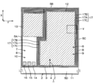
- FIG. 1 is a perspective view of a semiconductor device viewed from one direction.
- FIG. 2 is a block circuit diagram showing the electrical structure of the semiconductor device.
- FIG. 3 is a circuit diagram for explaining normal operation and active clamp operation of the semiconductor device.
- FIG. 4 is a waveform diagram of main electrical signals.
- FIG. 5 is a cross-sectional perspective view of region V shown in FIG.
- FIG. 6 is a graph obtained by actually measuring the relationship between the active clamping capacity and the area resistivity.
- FIG. 7 is a cross-sectional perspective view for explaining normal operation of the semiconductor device.
- FIG. 8 is a cross-sectional perspective view for explaining the active clamping operation of the semiconductor device.
- FIG. 9 is a block circuit diagram showing the semiconductor device according to the first embodiment.
- FIG. 10 is an equivalent circuit diagram representing the power MISFET of FIG. 9 as a first MISFET and a second MISFET.
- 11 is a circuit diagram showing a configuration example of the gate control circuit and the active clamp circuit in FIG. 10.
- FIG. 12 is a timing chart showing how the first Half-ON control of the power MISFET is performed during the active clamp operation.
- 13A and 13B are diagrams for explaining the active clamp operation in the output short-circuit state of the semiconductor device according to the first embodiment.
- FIG. FIG. 14 is a block circuit diagram showing the semiconductor device according to the second embodiment.
- FIG. 15 is a diagram showing a configuration example of a delay circuit according to the second embodiment.
- FIG. 16 is a diagram for explaining the active clamping operation of the semiconductor device according to the second embodiment.
- FIG. 17 is a block circuit diagram showing the semiconductor device according to the third embodiment.
- FIG. 18 is a diagram showing a configuration example of a delay circuit according to the third embodiment.
- FIG. 19 is a diagram (without a delay circuit) for explaining the active clamp operation of the semiconductor device according to the third embodiment;
- FIG. 20 is a diagram (with a delay circuit) for explaining the active clamp operation of the semiconductor device according to the third embodiment;
- FIG. 21 is an external view showing one configuration example of a vehicle.
- FIG. 1 is a perspective view of the semiconductor device 1 viewed from one direction.
- the semiconductor device 1 is not limited to a high-side switching device.
- the semiconductor device 1 can also be provided as a low-side switching device by adjusting the electrical connections or functions of various structures.
- semiconductor device 1 includes semiconductor layer 2 .
- the semiconductor layer 2 contains silicon.
- the semiconductor layer 2 is formed in the shape of a rectangular parallelepiped chip.
- the semiconductor layer 2 has a first main surface 3 on one side, a second main surface 4 on the other side, and side surfaces 5A, 5B, 5C, and 5D connecting the first main surface 3 and the second main surface 4. ing.
- the first main surface 3 and the second main surface 4 are formed in a quadrangular shape when viewed from the normal direction Z (hereinafter simply referred to as "plan view").
- the side surface 5A and the side surface 5C extend along the first direction X and face each other in a second direction Y intersecting the first direction X.
- the side surface 5B and the side surface 5D extend along the second direction Y and face each other in the first direction X.
- the second direction Y is, more specifically, orthogonal to the first direction X. As shown in FIG.
- An output area 6 and an input area 7 are set in the semiconductor layer 2 .
- the output area 6 is set in the area on the side of the side surface 5C.
- the input area 7 is set in the area on the side 5A side.
- the area SOUT of the output region 6 is greater than or equal to the area SIN of the input region 7 (SIN ⁇ SOUT).
- the ratio SOUT/SIN of the area SOUT to the area SIN may be 1 or more and 10 or less (1 ⁇ SOUT/SIN ⁇ 10).
- the ratio SOUT/SIN may be 1 or more and 2 or less, 2 or more and 4 or less, 4 or more and 6 or less, 6 or more and 8 or less, or 8 or more and 10 or less.
- the planar shape of the input area 7 and the planar shape of the output area 6 are arbitrary and are not limited to specific shapes. Of course, the ratio SOUT/SIN may be greater than 0 and less than 1.
- Power MISFET 9 includes a gate, drain and source.
- the power MISFET 9 functions as a high-side switch that conducts/disconnects between the power supply end and the load.
- the input area 7 includes a control IC (Integrated Circuit) 10 as an example of a control circuit.
- the control IC 10 includes multiple types of functional circuits that implement various functions.
- the plurality of types of functional circuits include circuits that generate gate control signals for driving and controlling the power MISFET 9 based on electrical signals from the outside.
- the control IC 10 forms a so-called IPD (Intelligent Power Device) together with the power MISFET 9 .
- the IPD is also called an IPM (Intelligent Power Module).
- the input area 7 is electrically isolated from the output area 6 by the area isolation structure 8 .
- the region isolation structures 8 are indicated by hatching. Although a detailed description is omitted, the region isolation structure 8 may have a trench isolation structure in which a trench is filled with an insulator.
- a plurality of (here, six) electrodes 11 , 12 , 13 , 14 , 15 , 16 are formed on the semiconductor layer 2 .
- a plurality of electrodes 11-16 are indicated by hatching.
- a plurality of electrodes 11 to 16 are formed as terminal electrodes that are externally connected by conducting wires (eg, bonding wires) or the like.
- the number, arrangement and planar shape of the plurality of electrodes 11 to 16 are arbitrary, and are not limited to the form shown in FIG.
- the number, arrangement and planar shape of the plurality of electrodes 11 to 16 are adjusted according to the specifications of the power MISFET 9 or the specifications of the control IC 10.
- the plurality of electrodes 11-16 includes, in this embodiment, a drain electrode 11 (power supply electrode), a source electrode 12 (output electrode), an input electrode 13, a reference voltage electrode 14, an ENABLE electrode 15 and a SENSE electrode 16.
- FIG. 11 power supply electrode
- FIG. 12 power supply electrode
- the drain electrode 11 is formed on the second main surface 4 of the semiconductor layer 2 . Drain electrode 11 is electrically connected to second main surface 4 of semiconductor layer 2 . The drain electrode 11 transmits the power supply voltage VB to the drain of the power MISFET 9 and various circuits of the control IC 10 .
- the drain electrode 11 may include at least one of a Ti layer, Ni layer, Au layer, Ag layer and Al layer.
- the drain electrode 11 may have a single layer structure including a Ti layer, Ni layer, Au layer, Ag layer or Al layer.
- the drain electrode 11 may have a laminated structure in which at least two of a Ti layer, a Ni layer, an Au layer, an Ag layer, and an Al layer are laminated in an arbitrary manner.
- the source electrode 12 is formed on the output region 6 on the first main surface 3 .
- Source electrode 12 is electrically connected to the source of power MISFET 9 .
- the source electrode 12 transmits an electric signal generated by the power MISFET 9 to the outside.
- the input electrode 13 , the reference voltage electrode 14 , the ENABLE electrode 15 and the SENSE electrode 16 are each formed on the input region 7 on the first main surface 3 .
- Input electrode 13 transmits an input voltage for driving control IC 10 .
- the reference voltage electrode 14 transmits a reference voltage (eg ground voltage) to the control IC 10 .
- ENABLE electrode 15 transmits an electrical signal for enabling or disabling some or all of the functions of control IC 10 .
- SENSE electrode 16 transmits an electrical signal for detecting an abnormality in control IC 10 .
- a gate control wiring 17 as an example of a control wiring is further formed on the semiconductor layer 2 .
- the gate control wiring 17 is selectively routed to the output region 6 and the input region 7 .
- the gate control wiring 17 is electrically connected to the gate of the power MISFET 9 in the output region 6 and electrically connected to the control IC 10 in the input region 7 .
- the gate control wiring 17 transmits the gate control signal generated by the control IC 10 to the gate of the power MISFET 9 .
- the gate control signals include on-signal Von and off-signal Voff, and control the on-state and off-state of power MISFET 9 .
- the ON signal Von is higher than the gate threshold voltage Vth of the power MISFET 9 (Vth ⁇ Von).
- the off signal Voff is lower than the gate threshold voltage Vth of the power MISFET 9 (Voff ⁇ Vth).
- the off signal Voff may be a reference voltage (eg ground voltage).
- the gate control wiring 17 includes a first gate control wiring 17A, a second gate control wiring 17B and a third gate control wiring 17C in this form.
- the first gate control wiring 17A, the second gate control wiring 17B and the third gate control wiring 17C are electrically insulated from each other.
- two first gate control wirings 17A are routed to different regions. Also, the two second gate control wirings 17B are routed to different regions. Also, the two third gate control wirings 17C are routed to different regions.
- the first gate control wiring 17A, the second gate control wiring 17B and the third gate control wiring 17C transmit the same or different gate control signals to the gates of the power MISFETs 9.
- the number, arrangement, shape, etc. of the gate control wiring 17 are arbitrary, and are adjusted according to the transmission distance of the gate control signal or the number of gate control signals to be transmitted.
- Source electrode 12, input electrode 13, reference voltage electrode 14, ENABLE electrode 15, SENSE electrode 16, and gate control wiring 17 each contain at least one of nickel, palladium, aluminum, copper, an aluminum alloy, and a copper alloy. You can
- the source electrode 12, the input electrode 13, the reference voltage electrode 14, the ENABLE electrode 15, the SENSE electrode 16 and the gate control wiring 17 are made of Al--Si--Cu (aluminum--silicon--copper) alloy, Al--Si (aluminum--silicon) alloy. , and at least one of an Al—Cu (aluminum-copper) alloy.
- the source electrode 12, the input electrode 13, the reference voltage electrode 14, the ENABLE electrode 15, the SENSE electrode 16, and the gate control wiring 17 may contain the same type of electrode material, or may contain mutually different electrode materials. .
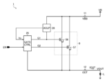
- FIG. 2 is a block circuit diagram showing the electrical structure of the semiconductor device 1 shown in FIG. A case where the semiconductor device 1 is mounted on a vehicle will be described below as an example.
- the semiconductor device 1 includes a drain electrode 11, a source electrode 12, an input electrode 13, a reference voltage electrode 14, an ENABLE electrode 15, a SENSE electrode 16, a gate control wiring 17, a power MISFET 9 and a control IC 10.
- the power supply voltage VB may be 10 V or more and 20 V or less.
- the input electrode 13 may be connected to an MCU (Micro Controller Unit), DC/DC converter, LDO (Low Drop Out), or the like. Input electrode 13 provides an input voltage to control IC 10 . The input voltage may be between 1V and 10V.
- the reference voltage electrode 14 is connected to the reference voltage wiring. Reference voltage electrode 14 provides a reference voltage to power MISFET 9 and control IC 10 .
- the ENABLE electrode 15 may be connected to the MCU. An electric signal for enabling or disabling some or all of the functions of the control IC 10 is input to the ENABLE electrode 15 .
- the SENSE electrode 16 may be connected to a resistor.
- a gate of the power MISFET 9 is connected to a control IC 10 (a gate control circuit 25 to be described later) via a gate control wiring 17 .
- a drain of the power MISFET 9 is connected to the drain electrode 11 .
- a source of the power MISFET 9 is connected to a control IC 10 (current detection circuit 27 to be described later) and a source electrode 12 .
- the control IC 10 includes a sensor MISFET 21, an input circuit 22, a current/voltage control circuit 23, a protection circuit 24, a gate control circuit 25, an active clamp circuit 26, a current detection circuit 27, a power reverse connection protection circuit 28, and an abnormality detection circuit 29. .
- a gate of the sensor MISFET 21 is connected to the gate control circuit 25 .
- a drain of the sensor MISFET 21 is connected to the drain electrode 11 .
- a source of the sensor MISFET 21 is connected to the current detection circuit 27 .
- the input circuit 22 is connected to the input electrode 13 and the current/voltage control circuit 23 .
- Input circuit 22 may include a Schmitt trigger circuit.
- the input circuit 22 shapes the waveform of the electrical signal applied to the input electrode 13 .
- a signal generated by the input circuit 22 is input to the current/voltage control circuit 23 .
- the current/voltage control circuit 23 is connected to a protection circuit 24 , a gate control circuit 25 , a power supply reverse connection protection circuit 28 and an abnormality detection circuit 29 .
- the current/voltage control circuit 23 may include a logic circuit.
- the current/voltage control circuit 23 generates various voltages according to the electrical signal from the input circuit 22 and the electrical signal from the protection circuit 24 .
- the current/voltage control circuit 23 includes a drive voltage generation circuit 30 , a first constant voltage generation circuit 31 , a second constant voltage generation circuit 32 and a reference voltage/reference current generation circuit 33 in this embodiment.
- the drive voltage generation circuit 30 generates a drive voltage for driving the gate control circuit 25 .
- the drive voltage may be set to a value obtained by subtracting a predetermined value from the power supply voltage VB.
- the drive voltage generation circuit 30 may generate a drive voltage of 5 V or more and 15 V or less by subtracting 5 V from the power supply voltage VB.
- a drive voltage is input to the gate control circuit 25 .
- the first constant voltage generation circuit 31 generates a first constant voltage for driving the protection circuit 24.
- the first constant voltage generation circuit 31 may include a Zener diode or a regulator circuit (here, a Zener diode).
- the first constant voltage may be 1 V or more and 5 V or less.
- the first constant voltage is input to the protection circuit 24 (more specifically, an open load detection circuit 35 and the like, which will be described later).
- the second constant voltage generation circuit 32 generates a second constant voltage for driving the protection circuit 24.
- the second constant voltage generation circuit 32 may include a Zener diode or a regulator circuit (regulator circuit here).
- the second constant voltage may be 1 V or more and 5 V or less.
- the second constant voltage is input to the protection circuit 24 (more specifically, an overheat protection circuit 36 and a low-voltage malfunction suppression circuit 37, which will be described later).
- the reference voltage/reference current generation circuit 33 generates reference voltages and reference currents for various circuits.
- the reference voltage may be 1 V or more and 5 V or less.
- the reference current may be 1 mA or more and 1 A or less.
- the reference voltage and reference current are input to various circuits. If the various circuits include comparators, the reference voltage and reference current may be input to the comparators.
- the protection circuit 24 is connected to the current/voltage control circuit 23 , the gate control circuit 25 , the abnormality detection circuit 29 , the source of the power MISFET 9 and the source of the sensor MISFET 21 .
- Protection circuit 24 includes an overcurrent protection circuit 34 , an open load detection circuit 35 , an overheat protection circuit 36 and a low voltage malfunction suppression circuit 37 .
- the overcurrent protection circuit 34 protects the power MISFET 9 from overcurrent.
- the overcurrent protection circuit 34 is connected to the source of the gate control circuit 25 and the sensor MISFET21.
- Overcurrent protection circuit 34 may include a current monitor circuit. A signal generated by the overcurrent protection circuit 34 is input to the gate control circuit 25 (more specifically, a drive signal output circuit 40 described later).
- the open load detection circuit 35 detects the short state and open state of the power MISFET 9 .
- the load open detection circuit 35 is connected to the current/voltage control circuit 23 and the source of the power MISFET 9 .
- a signal generated by the open load detection circuit 35 is input to the current/voltage control circuit 23 .
- the overheat protection circuit 36 monitors the temperature of the power MISFET 9 and protects the power MISFET 9 from excessive temperature rise.
- the overheat protection circuit 36 is connected to the current/voltage control circuit 23 .
- Thermal protection circuit 36 may include a temperature sensitive device such as a temperature sensitive diode or thermistor. A signal generated by the overheat protection circuit 36 is input to the current/voltage control circuit 23 .
- the low-voltage malfunction suppression circuit 37 suppresses malfunction of the power MISFET 9 when the power supply voltage VB is less than a predetermined value.
- the low voltage malfunction suppression circuit 37 is connected to the current/voltage control circuit 23 .
- a signal generated by the low-voltage malfunction suppression circuit 37 is input to the current/voltage control circuit 23 .
- the gate control circuit 25 controls the ON state and OFF state of the power MISFET 9 and the ON state and OFF state of the sensor MISFET 21 .
- the gate control circuit 25 is connected to the current/voltage control circuit 23 , the protection circuit 24 , the gate of the power MISFET 9 and the gate of the sensor MISFET 21 .
- the gate control circuit 25 generates a plurality of gate control signals corresponding to the number of gate control wirings 17 according to the electrical signal from the current/voltage control circuit 23 and the electrical signal from the protection circuit 24 .
- a plurality of gate control signals are input to the gate of the power MISFET 9 and the gate of the sensor MISFET 21 through the gate control wiring 17, respectively.
- the gate control circuit 25 collectively controls a plurality of gate control signals in response to an electrical signal (input signal) applied to the input electrode 13 to turn on/off the power MISFET 9, while active clamping is performed. It has a function of individually controlling a plurality of gate control signals so as to raise the on-resistance of the power MISFET 9 when the circuit 26 operates (details will be described later).
- the gate control circuit 25 more specifically includes an oscillation circuit 38, a charge pump circuit 39 and a drive signal output circuit 40.
- the oscillator circuit 38 oscillates according to the electrical signal from the current/voltage control circuit 23 and generates a predetermined electrical signal.
- An electrical signal generated by the oscillator circuit 38 is input to the charge pump circuit 39 .
- the charge pump circuit 39 boosts the electric signal from the oscillation circuit 38 .
- the electric signal boosted by the charge pump circuit 39 is input to the drive signal output circuit 40 .
- the drive signal output circuit 40 generates a plurality of gate control signals according to the electrical signal from the charge pump circuit 39 and the electrical signal from the protection circuit 24 (more specifically, the overcurrent protection circuit 34).
- a plurality of gate control signals are inputted to the gate of the power MISFET 9 and the gate of the sensor MISFET 21 via the gate control wiring 17 .
- Sensor MISFET 21 and power MISFET 9 are controlled simultaneously by gate control circuit 25 .
- the active clamp circuit 26 protects the power MISFET 9 from back electromotive force. Active clamp circuit 26 is connected to drain electrode 11 , the gate of power MISFET 9 and the gate of sensor MISFET 21 . Active clamp circuit 26 may include multiple diodes.
- the active clamp circuit 26 may include multiple diodes forward-biased to each other. Active clamp circuit 26 may include multiple diodes that are reverse biased together. The active clamp circuit 26 may include multiple diodes forward biased together and multiple diodes reverse biased together.
- the plurality of diodes may include pn junction diodes, Zener diodes, or pn junction diodes and Zener diodes.
- Active clamp circuit 26 may include multiple Zener diodes biased together.
- Active clamp circuit 26 may include a Zener diode and a pn junction diode that are reverse biased together.
- the current detection circuit 27 detects currents flowing through the power MISFET 9 and the sensor MISFET 21 .
- the current detection circuit 27 is connected to the protection circuit 24 , the abnormality detection circuit 29 , the source of the power MISFET 9 and the source of the sensor MISFET 21 .
- Current detection circuit 27 generates a current detection signal according to the electrical signal generated by power MISFET 9 and the electrical signal generated by sensor MISFET 21 .
- the current detection signal is input to the abnormality detection circuit 29 .
- the power supply reverse connection protection circuit 28 protects the current/voltage control circuit 23, the power MISFET 9, etc. from the reverse voltage when the power supply is reversely connected.
- a reverse power connection protection circuit 28 is connected to the reference voltage electrode 14 and the current/voltage control circuit 23 .
- the abnormality detection circuit 29 monitors the voltage of the protection circuit 24.
- the abnormality detection circuit 29 is connected to the current/voltage control circuit 23 , the protection circuit 24 and the current detection circuit 27 .
- an abnormality such as voltage fluctuation
- the abnormality detection circuit 29 detects the voltage of the protection circuit 24. Generates an abnormality detection signal according to the condition and outputs it to the outside.
- the abnormality detection circuit 29 more specifically includes a first multiplexer circuit 41 and a second multiplexer circuit 42 .
- the first multiplexer circuit 41 includes two inputs, one output and one selection control input. The input portion of the first multiplexer circuit 41 is connected to the protection circuit 24 and the current detection circuit 27, respectively.
- a second multiplexer circuit 42 is connected to the output of the first multiplexer circuit 41 .
- a current/voltage control circuit 23 is connected to the selection control input section of the first multiplexer circuit 41 .
- the first multiplexer circuit 41 generates an abnormality detection signal according to the electric signal from the current/voltage control circuit 23, the voltage detection signal from the protection circuit 24, and the current detection signal from the current detection circuit 27.
- the abnormality detection signal generated by the first multiplexer circuit 41 is input to the second multiplexer circuit 42 .
- the second multiplexer circuit 42 includes two inputs and one output.
- the input section of the second multiplexer circuit 42 is connected to the output section of the second multiplexer circuit 42 and the ENABLE electrode 15, respectively.
- the SENSE electrode 16 is connected to the output of the second multiplexer circuit 42 .
- an ON signal is input from the MCU to the ENABLE electrode 15 and an abnormality detection signal is taken out from the SENSE electrode 16 .
- the abnormality detection signal is converted into an electrical signal by a resistor connected to the SENSE electrode 16 .
- An abnormal state of the semiconductor device 1 is detected based on this electrical signal.
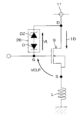
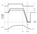
- FIG. 3 is a circuit diagram for explaining the active clamping operation of the semiconductor device 1 shown in FIG.
- FIG. 4 is a waveform diagram of main electrical signals in the circuit diagram shown in FIG.
- inductive load L is connected to the power MISFET 9.
- devices using windings (coils) such as solenoids, motors, transformers, and relays are exemplified as the inductive load L.
- Inductive load L is also referred to as L-load.
- the source of power MISFET 9 is connected to inductive load L.
- a drain of the power MISFET 9 is electrically connected to the drain electrode 11 .
- the gate and drain of power MISFET 9 are connected to active clamp circuit 26 .
- the active clamp circuit 26 includes m (m is a natural number) Zener diodes DZ and n (n is a natural number) pn junction diodes D in this circuit example.
- the pn junction diode D is reverse biased with respect to the Zener diode DZ.
- the power MISFET 9 switches from the OFF state to the ON state (normal operation).
- the ON signal Von has a voltage equal to or higher than the gate threshold voltage Vth (Vth ⁇ Von).
- the power MISFET 9 is kept on for a predetermined on-time TON.
- the drain current ID begins to flow from the drain of the power MISFET 9 to the source.
- the drain current ID increases from zero to a predetermined value and saturates.
- Inductive load L stores inductive energy due to the increase in drain current ID.
- the off signal Voff When the off signal Voff is input to the gate of the power MISFET 9, the power MISFET 9 switches from the on state to the off state.
- the off signal Voff has a voltage less than the gate threshold voltage Vth (Voff ⁇ Vth).
- the off signal Voff may be a reference voltage (eg ground voltage).
- the inductive energy of the inductive load L is applied to the power MISFET 9 as back electromotive force.
- the power MISFET 9 enters an active clamp state (active clamp operation).
- the source voltage VSS rapidly drops to a negative voltage lower than the reference voltage (ground voltage).
- the source voltage VSS is limited to a voltage equal to or higher than the voltage obtained by subtracting the limit voltage VL and the clamp-on voltage VCLP from the power supply voltage VB (VSS ⁇ VB ⁇ VL ⁇ VCLP). be.
- clamp voltage VDSSCL is limited by power MISFET 9 and active clamp circuit 26 to a voltage equal to or lower than the sum of clamp-on voltage VCLP and limit voltage VL (VDS ⁇ VCLP+VL).
- the clamp-on voltage VCLP is a positive voltage applied between the gate and source of the power MISFET 9 (that is, gate voltage VGS).
- the clamp-on voltage VCLP is equal to or higher than the gate threshold voltage Vth (Vth ⁇ VCLP). Therefore, power MISFET 9 maintains the ON state in the active clamp state.
- the power MISFET 9 is destroyed.
- the power MISFET 9 is designed so that the clamp voltage VDSSCL is equal to or less than the maximum rated drain voltage VDSS (VDSSCL ⁇ VDSS).
- VDSSCL When the clamp voltage VDSSCL is lower than the maximum rated drain voltage VDSS (VDSSCL ⁇ VDSS), the drain current ID continues to flow from the drain to the source of the power MISFET 9, and the inductive energy of the inductive load L is consumed (absorbed) in the power MISFET 9. be done.
- the drain current ID decreases from the peak value IAV immediately before the power MISFET 9 is turned off to zero after the active clamp time TAV.
- the gate voltage VGS becomes the reference voltage (for example, the ground voltage), and the power MISFET 9 is switched from the on state to the off state.
- the active clamp tolerance Eac of the power MISFET 9 is defined by the tolerance of the power MISFET 9 during active clamp operation. More specifically, the active clamp tolerance Eac is defined by the tolerance of the power MISFET 9 against back electromotive force generated due to the inductive energy of the inductive load L when the power MISFET 9 transitions from the ON state to the OFF state. be.
- the active clamp tolerance Eac is defined by the tolerance of the power MISFET 9 to energy generated due to the clamp voltage VDSSCL.
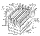
- FIG. 5 is a cross-sectional perspective view of region V shown in FIG.
- the upper structure of the first main surface 3 (the source electrode 12, the gate control wiring 17, the interlayer insulating layer, etc.) is omitted in this figure.
- the semiconductor layer 2 has a laminated structure including an n + -type semiconductor substrate 51 and an n-type epitaxial layer 52 in this embodiment.
- a second main surface 4 of the semiconductor layer 2 is formed by the semiconductor substrate 51 .
- the epitaxial layer 52 forms the first main surface 3 of the semiconductor layer 2 .
- Semiconductor substrate 51 and epitaxial layer 52 form side surfaces 5A to 5D of semiconductor layer 2 .
- the epitaxial layer 52 has an n-type impurity concentration less than the n-type impurity concentration of the semiconductor substrate 51 .
- the n-type impurity concentration of the semiconductor substrate 51 may be 1 ⁇ 10 18 cm ⁇ 3 or more and 1 ⁇ 10 20 cm ⁇ 3 or less.
- the n-type impurity concentration of the epitaxial layer 52 may be 1 ⁇ 10 15 cm ⁇ 3 or more and 1 ⁇ 10 18 cm ⁇ 3 or less.
- the epitaxial layer 52 has a thickness Tepi less than the thickness Tsub of the semiconductor substrate 51 (Tepi ⁇ Tsub).
- the thickness Tsub may be 50 ⁇ m or more and 450 ⁇ m or less.
- the thickness Tsub may be 50 ⁇ m to 150 ⁇ m, 150 ⁇ m to 250 ⁇ m, 250 ⁇ m to 350 ⁇ m, or 350 ⁇ m to 450 ⁇ m.
- the resistance value can be reduced by reducing the thickness Tsub.
- the thickness Tsub is adjusted by grinding.
- the second main surface 4 of the semiconductor layer 2 may be a ground surface having grinding marks.
- the thickness Tepi of the epitaxial layer 52 is preferably 1/10 or less of the thickness Tsub.
- the thickness Tepi may be 5 ⁇ m or more and 20 ⁇ m or less.
- the thickness Tepi may be between 5 ⁇ m and 10 ⁇ m, between 10 ⁇ m and 15 ⁇ m, or between 15 ⁇ m and 20 ⁇ m.
- the thickness Tepi is preferably 5 ⁇ m or more and 15 ⁇ m or less.
- a semiconductor substrate 51 is formed on the second main surface 4 side of the semiconductor layer 2 as a drain region 53 .
- the epitaxial layer 52 is formed in the surface layer portion of the first main surface 3 of the semiconductor layer 2 as a drift region 54 (drain drift region).
- the bottom of drift region 54 is formed by the boundary of semiconductor substrate 51 and epitaxial layer 52 .
- the epitaxial layer 52 is hereinafter referred to as a drift region 54 .
- a p-type body region 55 is formed in the surface layer portion of the first main surface 3 of the semiconductor layer 2 in the output region 6 .
- the body region 55 is the base region of the power MISFET 9 .
- the body region 55 may have a p-type impurity concentration of 1 ⁇ 10 16 cm ⁇ 3 or more and 1 ⁇ 10 18 cm ⁇ 3 or less.
- the body region 55 is formed on the surface layer of the drift region 54 .
- the bottom of body region 55 is formed in a region on the first main surface 3 side with respect to the bottom of drift region 54 .
- the thickness of the body region 55 may be 0.5 ⁇ m or more and 2 ⁇ m or less.
- the thickness of the body region 55 may be 0.5 ⁇ m or more and 1 ⁇ m or less, 1 ⁇ m or more and 1.5 ⁇ m or less, or 1.5 ⁇ m or more and 2 ⁇ m or less.
- the power MISFET 9 includes a first MISFET 56 (first transistor) and a second MISFET 57 (second transistor).
- the first MISFET 56 is electrically isolated from the second MISFET 57 and independently controlled.
- the second MISFET 57 is electrically isolated from the first MISFET 56 and independently controlled.
- the power MISFET 9 is configured to be driven when both the first MISFET 56 and the second MISFET 57 are in the ON state (Full-ON control). Also, the power MISFET 9 is configured to be driven while the first MISFET 56 is in the ON state and the second MISFET 57 is in the OFF state (first Half-ON control). Furthermore, the power MISFET 9 is configured to be driven while the first MISFET 56 is in the OFF state and the second MISFET 57 is in the ON state (second Half-ON control).
- the power MISFET 9 In the case of Full-ON control, the power MISFET 9 is driven with all current paths released. Therefore, the on-resistance in the semiconductor layer 2 is relatively lowered. On the other hand, in the case of the first Half-ON control or the second Half-ON control, the power MISFET 9 is driven with some current paths cut off. Therefore, the on-resistance in the semiconductor layer 2 relatively increases.
- the first MISFET 56 specifically includes a plurality of first FET (Field Effect Transistor) structures 58 .
- the plurality of first FET structures 58 are arranged at intervals along the first direction X and extend along the second direction Y in a strip shape, respectively, in plan view.
- the plurality of first FET structures 58 are formed in a stripe shape as a whole in plan view.
- the region on the one end side of the first FET structure 58 is illustrated, and the illustration of the region on the other end side of the first FET structure 58 is omitted.
- the structure of the region on the other end side of the first FET structure 58 is substantially the same as the structure of the region on the one end side of the first FET structure 58 .
- the structure of the region on the one end side of the first FET structure 58 will be described as an example, and the structure of the region on the other end side of the first FET structure 58 will be omitted.
- Each first FET structure 58 includes a first trench gate structure 60 in this form.
- the first width WT1 of the first trench gate structure 60 may be between 0.5 ⁇ m and 5 ⁇ m.
- the first width WT1 is the width in the direction (first direction X) orthogonal to the direction (second direction Y) in which the first trench gate structure 60 extends.
- the first width WT1 is 0.5 ⁇ m or more and 1 ⁇ m or less, 1 ⁇ m or more and 1.5 ⁇ m or less, 1.5 ⁇ m or more and 2 ⁇ m or less, 2 ⁇ m or more and 2.5 ⁇ m or less, 2.5 ⁇ m or more and 3 ⁇ m or less, 3 ⁇ m or more and 3.5 ⁇ m or less, It may be 3.5 ⁇ m or more and 4 ⁇ m or less, 4 ⁇ m or more and 4.5 ⁇ m or less, or 4.5 ⁇ m or more and 5 ⁇ m or less.
- the first width WT1 is preferably 0.8 ⁇ m or more and 1.2 ⁇ m or less.
- the first trench gate structure 60 penetrates the body region 55 and reaches the drift region 54 .
- the first depth DT1 of the first trench gate structure 60 may be 1 ⁇ m or more and 10 ⁇ m or less.
- the first depth DT1 may be 1 ⁇ m or more and 2 ⁇ m or less, 2 ⁇ m or more and 4 ⁇ m or less, 4 ⁇ m or more and 6 ⁇ m or less, 6 ⁇ m or more and 8 ⁇ m or less, or 8 ⁇ m or more and 10 ⁇ m or less.
- the first depth DT1 is preferably 2 ⁇ m or more and 6 ⁇ m or less.
- the first trench gate structure 60 includes a first sidewall 61 on one side, a second sidewall 62 on the other side, and a bottom wall 63 connecting the first sidewall 61 and the second sidewall 62 .
- the 1st side wall 61, the 2nd side wall 62, and the bottom wall 63 may be collectively called an “inner wall” or an “outer wall.”
- the absolute value of the angle (taper angle) formed between the first side wall 61 and the first main surface 3 in the semiconductor layer 2 may be more than 90° and 95° or less (for example, about 91°).
- the absolute value of the angle (taper angle) formed between second sidewall 62 and first main surface 3 in semiconductor layer 2 may be more than 90° and 95° or less (for example, about 91°).
- the first trench gate structure 60 may be formed in a tapered shape (tapered shape) in which the first width WT1 narrows from the first main surface 3 side toward the bottom wall 63 side in a cross-sectional view.
- the bottom wall 63 of the first trench gate structure 60 is located in a region on the first main surface 3 side with respect to the bottom of the drift region 54 .
- a bottom wall 63 of the first trench gate structure 60 is formed in a convex curved shape (U-shape) toward the bottom of the drift region 54 .
- the bottom wall 63 of the first trench gate structure 60 is located in the region on the first main surface 3 side with a first interval IT1 of 1 ⁇ m or more and 10 ⁇ m or less from the bottom of the drift region 54 .
- the first interval IT1 may be 1 ⁇ m or more and 2 ⁇ m or less, 2 ⁇ m or more and 4 ⁇ m or less, 4 ⁇ m or more and 6 ⁇ m or less, 6 ⁇ m or more and 8 ⁇ m or less, or 8 ⁇ m or more and 10 ⁇ m or less.
- the first interval IT1 is preferably 1 ⁇ m or more and 5 ⁇ m or less.
- the second MISFET 57 includes a plurality of second FET structures 68 in this form.
- the plurality of second FET structures 68 are arranged at intervals along the first direction X and extend along the second direction Y in a strip shape, respectively, in plan view.
- the multiple second FET structures 68 extend along the same direction as the multiple first FET structures 58 .
- the plurality of second FET structures 68 are formed in a stripe shape as a whole in plan view.
- the plurality of second FET structures 68 are alternately arranged with the plurality of first FET structures 58 in a manner that sandwiches one first FET structure 58 in this embodiment.
- the region on the one end side of the second FET structure 68 is illustrated, and the illustration of the region on the other end side of the second FET structure 68 is omitted.
- the structure of the region on the other end side of the second FET structure 68 is substantially the same as the structure of the region on the one end side of the second FET structure 68 .
- the structure of the region on the one end side of the second FET structure 68 will be described as an example, and the structure of the region on the other end side of the second FET structure 68 will be omitted.
- Each second FET structure 68 includes a second trench gate structure 70 in this form.
- a second width WT2 of the second trench gate structure 70 may be 0.5 ⁇ m or more and 5 ⁇ m or less.
- the second width WT2 is the width in the direction (first direction X) orthogonal to the direction (second direction Y) in which the second trench gate structure 70 extends.
- the second width WT2 is 0.5 ⁇ m or more and 1 ⁇ m or less, 1 ⁇ m or more and 1.5 ⁇ m or less, 1.5 ⁇ m or more and 2 ⁇ m or less, 2 ⁇ m or more and 2.5 ⁇ m or less, 2.5 ⁇ m or more and 3 ⁇ m or less, 3 ⁇ m or more and 3.5 ⁇ m or less, It may be 3.5 ⁇ m or more and 4 ⁇ m or less, 4 ⁇ m or more and 4.5 ⁇ m or less, or 4.5 ⁇ m or more and 5 ⁇ m or less.
- the second width WT2 is preferably 0.8 ⁇ m or more and 1.2 ⁇ m or less.
- the second width WT2 of the second trench gate structure 70 may be greater than or equal to the first width WT1 of the first trench gate structure 60 (WT1 ⁇ WT2).
- the second width WT2 may be less than or equal to the first width WT1 (WT1 ⁇ WT2).
- the second trench gate structure 70 penetrates the body region 55 and reaches the drift region 54.
- the second depth DT2 of the second trench gate structure 70 may be 1 ⁇ m or more and 10 ⁇ m or less.
- the second depth DT2 may be 1 ⁇ m or more and 2 ⁇ m or less, 2 ⁇ m or more and 4 ⁇ m or less, 4 ⁇ m or more and 6 ⁇ m or less, 6 ⁇ m or more and 8 ⁇ m or less, or 8 ⁇ m or more and 10 ⁇ m or less.
- the second depth DT2 is preferably 2 ⁇ m or more and 6 ⁇ m or less.
- the second depth DT2 of the second trench gate structure 70 may be greater than or equal to the first depth DT1 of the first trench gate structure 60 (DT1 ⁇ DT2).
- the second depth DT2 may be less than or equal to the first depth DT1 (DT1 ⁇ DT2).
- the second trench gate structure 70 includes a first sidewall 71 on one side, a second sidewall 72 on the other side, and a bottom wall 73 connecting the first sidewall 71 and the second sidewall 72 .
- the 1st side wall 71, the 2nd side wall 72, and the bottom wall 73 may be collectively called an “inner wall” or an “outer wall.”
- the absolute value of the angle (taper angle) formed between the first sidewall 71 and the first main surface 3 in the semiconductor layer 2 may be more than 90° and 95° or less (for example, about 91°).
- the absolute value of the angle (taper angle) formed between second side wall 72 and first main surface 3 in semiconductor layer 2 may be more than 90° and 95° or less (for example, about 91°).
- the second trench gate structure 70 may be formed in a tapered shape (tapered shape) in which the second width WT2 narrows from the first main surface 3 side toward the bottom wall 73 side in a cross-sectional view.
- the bottom wall 73 of the second trench gate structure 70 is located in a region on the first main surface 3 side with respect to the bottom of the drift region 54 .
- a bottom wall 73 of the second trench gate structure 70 is formed in a convex curved shape (U-shape) toward the bottom of the drift region 54 .
- the bottom wall 73 of the second trench gate structure 70 is located in the region on the first main surface 3 side with a second distance IT2 of 1 ⁇ m or more and 10 ⁇ m or less from the bottom of the drift region 54 .
- the second interval IT2 may be 1 ⁇ m or more and 2 ⁇ m or less, 2 ⁇ m or more and 4 ⁇ m or less, 4 ⁇ m or more and 6 ⁇ m or less, 6 ⁇ m or more and 8 ⁇ m or less, or 8 ⁇ m or more and 10 ⁇ m or less.
- the second interval IT2 is preferably 1 ⁇ m or more and 5 ⁇ m or less.
- a cell region 75 is defined in each region between the plurality of first trench gate structures 60 and the plurality of second trench gate structures 70 .
- the plurality of cell regions 75 are arranged at intervals along the first direction X in a plan view, and each extend in a band shape along the second direction Y. As shown in FIG.
- a plurality of cell regions 75 extend along the same direction as the first trench gate structure 60 and the second trench gate structure 70 .
- the plurality of cell regions 75 are formed in a stripe shape as a whole in plan view.
- a first depletion layer extends into the drift region 54 from the outer wall of the first trench gate structure 60 .
- the first depletion layer extends from the outer wall of the first trench gate structure 60 in the direction along the first main surface 3 and the normal direction Z.
- a second depletion layer extends into the drift region 54 from the outer wall of the second trench gate structure 70 .
- the second depletion layer extends from the outer wall of the second trench gate structure 70 in the direction along the first main surface 3 and the normal direction Z.
- the second trench gate structure 70 is spaced apart from the first trench gate structure 60 in such a manner that the second depletion layer overlaps the first depletion layer. That is, the second depletion layer overlaps the first depletion layer in the cell region 75 in the region on the first main surface 3 side with respect to the bottom wall 73 of the second trench gate structure 70 . According to such a structure, it is possible to suppress the electric field from concentrating on the first trench gate structure 60 and the second trench gate structure 70, thereby suppressing a decrease in the breakdown voltage.
- the second depletion layer preferably overlaps the first depletion layer in a region on the bottom side of the drift region 54 with respect to the bottom wall 73 of the second trench gate structure 70 . According to such a structure, concentration of an electric field on the bottom wall 63 of the first trench gate structure 60 and the bottom wall 73 of the second trench gate structure 70 can be suppressed, so that a decrease in breakdown voltage can be suppressed appropriately. .
- the pitch PS between sidewalls of the first trench gate structure 60 and the second trench gate structure 70 may be 0.2 ⁇ m or more and 2 ⁇ m or less.
- the pitch PS is between the first sidewall 61 (second sidewall 62) of the first trench gate structure 60 and the second sidewall 72 (first sidewall 71) of the second trench gate structure 70 between the first trench gate structure 60 and It is the distance in the direction (first direction X) orthogonal to the direction (second direction Y) in which the second trench gate structure 70 extends.
- the pitch PS is 0.2 ⁇ m or more and 0.4 ⁇ m or less, 0.4 ⁇ m or more and 0.6 ⁇ m or less, 0.6 ⁇ m or more and 0.8 ⁇ m or less, 0.8 ⁇ m or more and 1.0 ⁇ m or less, 1.0 ⁇ m or more and 1.2 ⁇ m or less, 1 2 ⁇ m or more and 1.4 ⁇ m or less, 1.4 ⁇ m or more and 1.6 ⁇ m or less, 1.6 ⁇ m or more and 1.8 ⁇ m or less, or 1.8 ⁇ m or more and 2.0 ⁇ m or less.
- the pitch PS is preferably 0.3 ⁇ m or more and 1.5 ⁇ m or less.
- the pitch PC between the central portions of the first trench gate structure 60 and the second trench gate structure 70 may be 1 ⁇ m or more and 7 ⁇ m or less.
- the pitch PC is in the direction in which the first trench gate structure 60 and the second trench gate structure 70 extend (the second direction Y) between the central portion of the first trench gate structure 60 and the central portion of the second trench gate structure 70. It is the distance in the orthogonal direction (first direction X).
- the pitch PC may be 1 ⁇ m or more and 2 ⁇ m or less, 2 ⁇ m or more and 3 ⁇ m or less, 3 ⁇ m or more and 4 ⁇ m or less, 4 ⁇ m or more and 5 ⁇ m or less, 5 ⁇ m or more and 6 ⁇ m or less, or 6 ⁇ m or more and 7 ⁇ m or less.
- the pitch PC is preferably 1 ⁇ m or more and 3 ⁇ m or less.
- the first trench gate structure 60 more specifically includes a first gate trench 81 , a first insulating layer 82 and a first electrode 83 .
- the first gate trench 81 is formed by digging the first main surface 3 toward the second main surface 4 side.
- the first gate trench 81 defines a first sidewall 61 , a second sidewall 62 and a bottom wall 63 of the first trench gate structure 60 .
- the first sidewall 61 , the second sidewall 62 and the bottom wall 63 of the first trench gate structure 60 are hereinafter also referred to as the first sidewall 61 , the second sidewall 62 and the bottom wall 63 of the first gate trench 81 .
- the first insulating layer 82 is formed like a film along the inner wall of the first gate trench 81 .
- the first insulating layer 82 defines a recessed space within the first gate trench 81 .
- a portion of the first insulating layer 82 covering the bottom wall 63 of the first gate trench 81 is formed along the bottom wall 63 of the first gate trench 81 .
- the first insulating layer 82 defines a U-shaped space recessed in a U-shape in the first gate trench 81 .
- the first insulating layer 82 is at least one of silicon oxide (SiO 2 ), silicon nitride (SiN), aluminum oxide (Al 2 O 3 ), zirconium oxide (ZrO 2 ), and tantalum oxide (Ta 2 O 3 ). including.
- the first insulating layer 82 may have a laminated structure including a SiN layer and a SiO 2 layer laminated in this order from the semiconductor layer 2 side.
- the first insulating layer 82 may have a laminated structure including a SiO 2 layer and a SiN layer laminated in this order from the semiconductor layer 2 side.
- the first insulating layer 82 may have a single layer structure consisting of a SiO2 layer or a SiN layer.
- the first insulating layer 82 has a single-layer structure consisting of a SiO 2 layer in this embodiment.
- the first insulating layer 82 includes a first bottom-side insulating layer 84 and a first opening-side insulating layer 85 formed in this order from the bottom wall 63 side of the first gate trench 81 toward the first main surface 3 side.
- the first bottom-side insulating layer 84 covers the inner wall of the first gate trench 81 on the bottom wall 63 side. More specifically, the first bottom-side insulating layer 84 covers the inner wall of the first gate trench 81 on the bottom wall 63 side with respect to the bottom of the body region 55 .
- the first bottom insulating layer 84 defines a U-shaped space on the bottom wall 63 side of the first gate trench 81 .
- the first bottom insulating layer 84 has a smooth inner wall surface defining a U-shaped space.
- a first bottom insulating layer 84 contacts the drift region 54 .
- a portion of the first bottom insulating layer 84 may contact the body region 55 .
- the first opening side insulating layer 85 covers the inner wall of the first gate trench 81 on the opening side. More specifically, the first opening side insulating layer 85 covers the first sidewall 61 and the second sidewall 62 of the first gate trench 81 in the region on the opening side of the first gate trench 81 with respect to the bottom of the body region 55 . covered. The first opening side insulating layer 85 is in contact with the body region 55 . A portion of the first opening side insulating layer 85 may be in contact with the drift region 54 .
- the first bottom insulating layer 84 has a first thickness T1.
- the first opening side insulating layer 85 has a second thickness T2 (T2 ⁇ T1) less than the first thickness T1.
- the first thickness T1 is the thickness along the normal direction of the inner wall of the first gate trench 81 in the first bottom-side insulating layer 84 .
- the second thickness T2 is the thickness along the normal direction of the inner wall of the first gate trench 81 in the first opening side insulating layer 85 .
- the first ratio T1/WT1 of the first thickness T1 to the first width WT1 of the first gate trench 81 may be 0.1 or more and 0.4 or less.
- the first ratio T1/WT1 is 0.1 or more and 0.15 or less, 0.15 or more and 0.2 or less, 0.2 or more and 0.25 or less, 0.25 or more and 0.3 or less, or 0.3 or more. It may be 0.35 or less, or 0.35 or more and 0.4 or less.
- the first ratio T1/WT1 is preferably 0.25 or more and 0.35 or less.
- the first thickness T1 of the first bottom-side insulating layer 84 may be 1500 ⁇ or more and 4000 ⁇ or less.
- the first thickness T1 may be 1500 ⁇ to 2000 ⁇ , 2000 ⁇ to 2500 ⁇ , 2500 ⁇ to 3000 ⁇ , 3000 ⁇ to 3500 ⁇ , or 3500 ⁇ to 4000 ⁇ .
- the first thickness T1 is preferably 1800 ⁇ or more and 3500 ⁇ or less.
- the first thickness T1 may be adjusted to 4000 ⁇ or more and 12000 ⁇ or less according to the first width WT1 of the first gate trench 81 .
- the first thickness T1 is 4000 ⁇ to 5000 ⁇ , 5000 ⁇ to 6000 ⁇ , 6000 ⁇ to 7000 ⁇ , 7000 ⁇ to 8000 ⁇ , 8000 ⁇ to 9000 ⁇ , 9000 ⁇ to 10000 ⁇ , 10000 ⁇ to 11000 ⁇ , or 11000 ⁇ to 12000 ⁇ .
- the breakdown voltage of the semiconductor device 1 can be increased by increasing the thickness of the first bottom-side insulating layer 84 .
- the second thickness T2 of the first opening-side insulating layer 85 may be 1/100 or more and 1/10 or less of the first thickness T1 of the first bottom-side insulating layer 84 .
- the second thickness T2 may range from 100 ⁇ to 500 ⁇ .
- the second thickness T2 may be 100 ⁇ to 200 ⁇ , 200 ⁇ to 300 ⁇ , 300 ⁇ to 400 ⁇ , or 400 ⁇ to 500 ⁇ .
- the second thickness T2 is preferably 200 ⁇ or more and 400 ⁇ or less.
- the first bottom-side insulating layer 84 has a first thickness T1 from a portion covering the first sidewall 61 and the second sidewall 62 of the first gate trench 81 toward a portion covering the bottom wall 63 of the first gate trench 81 . is formed in a manner of decreasing.
- the thickness of the portion of the first bottom-side insulating layer 84 covering the bottom wall 63 of the first gate trench 81 is such that the thickness of the first bottom-side insulating layer 84 covers the first side wall 61 and the second side wall 62 of the first gate trench 81 . Less than the thickness of the part to be covered.
- the width of the opening on the bottom wall side of the U-shaped space partitioned by the first bottom-side insulating layer 84 is expanded by the reduction of the first thickness T1. This suppresses the tapering of the U-shaped space.
- Such a U-shaped space is formed, for example, by etching the inner wall of the first bottom-side insulating layer 84 (for example, wet etching).
- the first electrode 83 is embedded in the first gate trench 81 with the first insulating layer 82 interposed therebetween.
- a first gate control signal (first control signal) including an ON signal Von and an OFF signal Voff is applied to the first electrode 83 .
- the first electrode 83 in this embodiment has an isolation split electrode structure including a first bottom electrode 86 , a first opening electrode 87 and a first intermediate insulating layer 88 .
- the first bottom electrode 86 is buried on the bottom wall 63 side of the first gate trench 81 with the first insulating layer 82 interposed therebetween. More specifically, the first bottom-side electrode 86 is buried on the bottom wall 63 side of the first gate trench 81 with the first bottom-side insulating layer 84 interposed therebetween. The first bottom-side electrode 86 faces the drift region 54 with the first bottom-side insulating layer 84 interposed therebetween. A portion of the first bottom electrode 86 may face the body region 55 with the first bottom insulating layer 84 interposed therebetween.
- the first bottom-side electrode 86 defines a recess having an inverted concave shape in a cross-sectional view between the first bottom-side insulating layer 84 and the first opening-side insulating layer 85 on the opening side of the first gate trench 81 . .
- local electric field concentration on the first bottom electrode 86 can be suppressed, so that a decrease in breakdown voltage can be suppressed.
- the first bottom electrode 86 is tapered from the top end to the bottom end. It can be suppressed appropriately. Thereby, local electric field concentration on the lower end portion of the first bottom electrode 86 can be appropriately suppressed.
- the first bottom electrode 86 may include at least one of conductive polysilicon, tungsten, aluminum, copper, aluminum alloys and copper alloys.
- First bottom electrode 86 comprises conductive polysilicon in this form.
- the conductive polysilicon may contain n-type impurities or p-type impurities.
- the conductive polysilicon preferably contains n-type impurities.
- the first opening side electrode 87 is embedded in the opening side of the first gate trench 81 with the first insulating layer 82 interposed therebetween. More specifically, the first opening-side electrode 87 is embedded in an inverted concave recess defined on the opening side of the first gate trench 81 with the first opening-side insulating layer 85 interposed therebetween. The first opening-side electrode 87 faces the body region 55 with the first opening-side insulating layer 85 interposed therebetween. A portion of the first opening-side electrode 87 may face the drift region 54 with the first opening-side insulating layer 85 interposed therebetween.
- the first opening side electrode 87 may contain at least one of conductive polysilicon, tungsten, aluminum, copper, aluminum alloy and copper alloy.
- the first aperture side electrode 87 preferably comprises the same type of conductive material as the first bottom side electrode 86 .
- the first opening-side electrode 87 contains conductive polysilicon in this form.
- the conductive polysilicon may contain n-type impurities or p-type impurities.
- the conductive polysilicon preferably contains n-type impurities.
- the first intermediate insulating layer 88 is interposed between the first bottom-side electrode 86 and the first opening-side electrode 87 and electrically insulates the first bottom-side electrode 86 and the first opening-side electrode 87 . More specifically, the first intermediate insulating layer 88 covers the first bottom-side electrode 86 exposed from the first bottom-side insulating layer 84 in the region between the first bottom-side electrode 86 and the first opening-side electrode 87. are doing. A first intermediate insulating layer 88 covers the upper end (more specifically, the protrusion) of the first bottom electrode 86 . The first intermediate insulating layer 88 is continuous with the first insulating layer 82 (the first bottom side insulating layer 84).
- the first intermediate insulating layer 88 has a third thickness T3.
- the third thickness T3 is less than the first thickness T1 of the first bottom insulating layer 84 (T3 ⁇ T1).
- the third thickness T3 may be 1/100 or more and 1/10 or less of the first thickness T1.
- the third thickness T3 may range from 100 ⁇ to 500 ⁇ .
- the third thickness T3 may be 100 ⁇ to 200 ⁇ , 200 ⁇ to 300 ⁇ , 300 ⁇ to 400 ⁇ , or 400 ⁇ to 500 ⁇ .
- the third thickness T3 is preferably 200 ⁇ or more and 400 ⁇ or less.
- the first intermediate insulating layer 88 is made of at least one of silicon oxide (SiO 2 ), silicon nitride (SiN), aluminum oxide (Al 2 O 3 ), zirconium oxide (ZrO 2 ), and tantalum oxide (Ta 2 O 3 ). Contains seeds.
- the first intermediate insulating layer 88 has a single layer structure consisting of a SiO 2 layer in this embodiment.
- the exposed portion of the first opening side electrode 87 exposed from the first gate trench 81 is positioned on the bottom wall 63 side of the first gate trench 81 with respect to the first main surface 3 in this embodiment.
- the exposed portion of the first opening side electrode 87 is curved toward the bottom wall 63 of the first gate trench 81 .
- the exposed portion of the first opening side electrode 87 is covered with a first cap insulating layer formed in a film shape.
- the first cap insulating layer continues to the first insulating layer 82 (first opening side insulating layer 85 ) in the first gate trench 81 .
- the first cap insulating layer may contain silicon oxide (SiO 2 ).
- Each first FET structure 58 further includes a p-type first channel region 91 (first channel).
- the first channel region 91 is formed in a region of the body region 55 facing the first electrode 83 (first opening side electrode 87) with the first insulating layer 82 (first opening side insulating layer 85) interposed therebetween.
- the first channel region 91 is formed along the first sidewall 61 or the second sidewall 62 or the first sidewall 61 and the second sidewall 62 of the first trench gate structure 60 .
- the first channel region 91 is formed along the first sidewall 61 and the second sidewall 62 of the first trench gate structure 60 in this configuration.
- Each first FET structure 58 further includes an n + -type first source region 92 formed in the surface layer of the body region 55 .
- First source region 92 defines a first channel region 91 in body region 55 with drift region 54 .
- the n-type impurity concentration of the first source region 92 exceeds the n-type impurity concentration of the drift region 54 .
- the n-type impurity concentration of the first source region 92 may be 1 ⁇ 10 19 cm ⁇ 3 or more and 1 ⁇ 10 21 cm ⁇ 3 or less.
- Each first FET structure 58 includes a plurality of first source regions 92 in this form.
- a plurality of first source regions 92 are formed at intervals along the first trench gate structure 60 in the surface layer portion of the body region 55 . More specifically, the plurality of first source regions 92 are formed along the first sidewall 61 or the second sidewall 62, or the first sidewall 61 and the second sidewall 62 of the first trench gate structure 60. .
- a plurality of first source regions 92 are spaced along first sidewall 61 and second sidewall 62 of first trench gate structure 60 in this configuration.
- the bottoms of the plurality of first source regions 92 are located in a region on the first main surface 3 side with respect to the bottoms of the body regions 55 .
- the plurality of first source regions 92 face the first electrode 83 (first opening side electrode 87) with the first insulating layer 82 (first opening side insulating layer 85) interposed therebetween.
- the first channel region 91 of the first MISFET 56 is formed in the body region 55 sandwiched between the plurality of first source regions 92 and the drift region 54 .
- Each first FET structure 58 further includes a p + -type first contact region 93 formed in the surface layer of the body region 55 .
- the p-type impurity concentration of the first contact region 93 exceeds the p-type impurity concentration of the body region 55 .
- the p-type impurity concentration of the first contact region 93 may be, for example, 1 ⁇ 10 19 cm ⁇ 3 or more and 1 ⁇ 10 21 cm ⁇ 3 or less.
- Each first FET structure 58 includes a plurality of first contact regions 93 in this form.
- a plurality of first contact regions 93 are formed at intervals along the first trench gate structure 60 in the surface layer portion of the body region 55 . More specifically, the plurality of first contact regions 93 are formed along the first sidewall 61 or the second sidewall 62, or the first sidewall 61 and the second sidewall 62 of the first trench gate structure 60. .
- a plurality of first contact regions 93 are spaced apart along the first sidewall 61 and the second sidewall 62 of the first trench gate structure 60 in this embodiment. More specifically, the multiple first contact regions 93 are formed in the surface layer portion of the body region 55 in an alternate arrangement with respect to the multiple first source regions 92 . The bottoms of the plurality of first contact regions 93 are located in a region on the first main surface 3 side with respect to the bottoms of the body regions 55 .
- a second trench gate structure 70 includes a second gate trench 101 , a second insulating layer 102 and a second electrode 103 .
- the second gate trench 101 is formed by digging the first main surface 3 toward the second main surface 4 side.
- the second gate trench 101 defines a first sidewall 71 , a second sidewall 72 and a bottom wall 73 of the second trench gate structure 70 .
- the first sidewall 71 , the second sidewall 72 and the bottom wall 73 of the second trench gate structure 70 are hereinafter also referred to as the first sidewall 71 , the second sidewall 72 and the bottom wall 73 of the second gate trench 101 .
- the second insulating layer 102 is formed like a film along the inner wall of the second gate trench 101 .
- the second insulating layer 102 defines a recessed space within the second gate trench 101 .
- a portion of the second insulating layer 102 covering the bottom wall 73 of the second gate trench 101 is formed along the bottom wall 73 of the second gate trench 101 .
- the second insulating layer 102 defines a U-shaped space recessed in a U-shape inside the second gate trench 101 .
- the second insulating layer 102 is made of at least one of silicon oxide (SiO 2 ), silicon nitride (SiN), aluminum oxide (Al 2 O 3 ), zirconium oxide (ZrO 2 ), and tantalum oxide (Ta 2 O 3 ). including.
- the second insulating layer 102 may have a laminated structure including a SiN layer and a SiO 2 layer laminated in this order from the semiconductor layer 2 side.
- the second insulating layer 102 may have a laminated structure including a SiO 2 layer and a SiN layer laminated in this order from the semiconductor layer 2 side.
- the second insulating layer 102 may have a single layer structure consisting of a SiO2 layer or a SiN layer.
- the second insulating layer 102 has a single layer structure consisting of a SiO 2 layer in this embodiment.
- the second insulating layer 102 includes a second bottom side insulating layer 104 and a second opening side insulating layer 105 formed in this order from the bottom wall 73 side of the second gate trench 101 toward the first main surface 3 side.
- the second bottom-side insulating layer 104 covers the inner wall of the second gate trench 101 on the bottom wall 73 side. More specifically, the second bottom-side insulating layer 104 covers the inner wall of the second gate trench 101 on the bottom wall 73 side with respect to the bottom of the body region 55 .
- the second bottom-side insulating layer 104 defines a U-shaped space on the bottom wall 73 side of the second gate trench 101 .
- the second bottom insulating layer 104 has a smooth inner wall surface defining a U-shaped space.
- a second bottom insulating layer 104 contacts the drift region 54 .
- a portion of the second bottom insulating layer 104 may contact the body region 55 .
- the second opening side insulating layer 105 covers the opening side inner wall of the second gate trench 101 . More specifically, the second opening-side insulating layer 105 covers the first sidewall 71 and the second sidewall 72 of the second gate trench 101 in the region on the opening side of the second gate trench 101 with respect to the bottom of the body region 55 . covered. The second opening side insulating layer 105 is in contact with the body region 55 . A portion of the second opening side insulating layer 105 may be in contact with the drift region 54 .
- the second bottom insulating layer 104 has a fourth thickness T4.
- the second opening side insulating layer 105 has a fifth thickness T5 (T5 ⁇ T4) less than the fourth thickness T4.
- the fourth thickness T4 is the thickness along the normal direction of the inner wall of the second gate trench 101 in the second bottom side insulating layer 104 .
- the fifth thickness T5 is the thickness along the normal direction of the inner wall of the second gate trench 101 in the second opening side insulating layer 105 .
- a second ratio T4/WT2 of the fourth thickness T4 to the second width WT2 of the second gate trench 101 may be 0.1 or more and 0.4 or less.
- the second ratio T4/WT2 is 0.1 or more and 0.15 or less, 0.15 or more and 0.2 or less, 0.2 or more and 0.25 or less, 0.25 or more and 0.3 or less, or 0.3 or more. It may be 0.35 or less, or 0.35 or more and 0.4 or less.
- the second ratio T4/WT2 is preferably 0.25 or more and 0.35 or less.
- the second ratio T4/WT2 may be less than or equal to the first ratio T1/WT1 (T4/WT2 ⁇ T1/WT1).
- the second ratio T4/WT2 may be greater than or equal to the first ratio T1/WT1 (T4/WT2 ⁇ T1/WT1).
- the fourth thickness T4 of the second bottom-side insulating layer 104 may be 1500 ⁇ or more and 4000 ⁇ or less.
- the fourth thickness T4 may be 1500 ⁇ to 2000 ⁇ , 2000 ⁇ to 2500 ⁇ , 2500 ⁇ to 3000 ⁇ , 3000 ⁇ to 3500 ⁇ , or 3500 ⁇ to 4000 ⁇ .
- the fourth thickness T4 is preferably 1800 ⁇ or more and 3500 ⁇ or less.
- the fourth thickness T4 may be 4000 ⁇ or more and 12000 ⁇ or less depending on the second width WT2 of the second gate trench 101 .
- the fourth thickness T4 is 4000 ⁇ to 5000 ⁇ , 5000 ⁇ to 6000 ⁇ , 6000 ⁇ to 7000 ⁇ , 7000 ⁇ to 8000 ⁇ , 8000 ⁇ to 9000 ⁇ , 9000 ⁇ to 10000 ⁇ , 10000 ⁇ to 11000 ⁇ , or 11000 ⁇ to 12000 ⁇ .
- the breakdown voltage of the semiconductor device 1 can be increased by thickening the second bottom-side insulating layer 104 .
- the fourth thickness T4 may be equal to or less than the first thickness T1 (T4 ⁇ T1).
- the fourth thickness T4 may be greater than or equal to the first thickness T1 (T4 ⁇ T1).
- the fifth thickness T5 of the second opening-side insulating layer 105 is less than the fourth thickness T4 of the second bottom-side insulating layer 104 (T5 ⁇ T4).
- the fifth thickness T5 may be 1/100 or more and 1/10 or less of the fourth thickness T4. It may be 100 ⁇ or more and 500 ⁇ or less.
- the fifth thickness T5 may be 100 ⁇ to 200 ⁇ , 200 ⁇ to 300 ⁇ , 300 ⁇ to 400 ⁇ , or 400 ⁇ to 500 ⁇ .
- the fifth thickness T5 is preferably 200 ⁇ or more and 400 ⁇ or less.
- the fifth thickness T5 may be equal to or less than the second thickness T2 (T5 ⁇ T2).
- the fifth thickness T5 may be greater than or equal to the second thickness T2 (T5 ⁇ T2).
- Second bottom-side insulating layer 104 has a fourth thickness T4 from a portion covering first sidewall 71 and second sidewall 72 of second gate trench 101 to a portion covering bottom wall 73 of second gate trench 101 . is formed in a manner of decreasing.
- the thickness of the portion of the second bottom-side insulating layer 104 covering the bottom wall 73 of the second gate trench 101 is such that the thickness of the second bottom-side insulating layer 104 covers the first side wall 71 and the second side wall 72 of the second gate trench 101 . Less than the thickness of the part to be covered.
- the width of the opening on the bottom wall side of the U-shaped space defined by the second bottom-side insulating layer 104 is expanded by the reduction of the fourth thickness T4. This suppresses the tapering of the U-shaped space.
- Such a U-shaped space is formed, for example, by etching the inner wall of the second bottom-side insulating layer 104 (for example, wet etching).
- the second electrode 103 is embedded in the second gate trench 101 with the second insulating layer 102 interposed therebetween.
- a predetermined second gate control signal (second control signal) including an ON signal Von and an OFF signal Voff is applied to the second electrode 103 .
- the second electrode 103 has, in this form, an insulation isolation type split electrode structure including a second bottom electrode 106, a second opening side electrode 107 and a second intermediate insulating layer .
- the second bottom electrode 106 is electrically connected to the first bottom electrode 86 in this configuration.
- the second aperture-side electrode 107 is electrically insulated from the first aperture-side electrode 87 .
- the second bottom electrode 106 is buried on the bottom wall 73 side of the second gate trench 101 with the second insulating layer 102 interposed therebetween. More specifically, the second bottom-side electrode 106 is buried on the bottom wall 73 side of the second gate trench 101 with the second bottom-side insulating layer 104 interposed therebetween. The second bottom-side electrode 106 faces the drift region 54 with the second bottom-side insulating layer 104 interposed therebetween. A portion of the second bottom-side electrode 106 may face the body region 55 with the second bottom-side insulating layer 104 interposed therebetween.
- the second bottom-side electrode 106 defines a recess having an inverted concave shape in a cross-sectional view between the second bottom-side insulating layer 104 and the second opening-side insulating layer 105 on the opening side of the second gate trench 101 . .
- local electric field concentration on the second bottom-side electrode 106 can be suppressed, so a decrease in breakdown voltage can be suppressed.
- the second bottom electrode 106 is tapered from the top end to the bottom end. It can be suppressed appropriately. As a result, local electric field concentration on the lower end portion of the second bottom electrode 106 can be appropriately suppressed.
- the second bottom electrode 106 may include at least one of conductive polysilicon, tungsten, aluminum, copper, aluminum alloys and copper alloys.
- the second bottom electrode 106 comprises conductive polysilicon in this form.
- the conductive polysilicon may contain n-type impurities or p-type impurities.
- the conductive polysilicon preferably contains n-type impurities.
- the second opening side electrode 107 is embedded in the opening side of the second gate trench 101 with the second insulating layer 102 interposed therebetween. More specifically, the second opening-side electrode 107 is embedded in an inverted concave recess defined on the opening side of the second gate trench 101 with the second opening-side insulating layer 105 interposed therebetween. The second opening-side electrode 107 faces the body region 55 with the second opening-side insulating layer 105 interposed therebetween. A portion of the second opening-side electrode 107 may face the drift region 54 with the second opening-side insulating layer 105 interposed therebetween.
- the second opening side electrode 107 may contain at least one of conductive polysilicon, tungsten, aluminum, copper, aluminum alloy and copper alloy.
- the second aperture side electrode 107 preferably comprises the same type of conductive material as the second bottom side electrode 106 .
- the second opening side electrode 107 contains conductive polysilicon in this form.
- the conductive polysilicon may contain n-type impurities or p-type impurities.
- the conductive polysilicon preferably contains n-type impurities.
- the second intermediate insulating layer 108 is interposed between the second bottom-side electrode 106 and the second opening-side electrode 107 to electrically insulate the second bottom-side electrode 106 and the second opening-side electrode 107 .
- the second intermediate insulating layer 108 more specifically covers the second bottom side electrode 106 exposed from the second bottom side insulating layer 104 in the region between the second bottom side electrode 106 and the second opening side electrode 107. are doing.
- a second intermediate insulating layer 108 covers the upper end (more specifically, the protrusion) of the second bottom electrode 106 .
- the second intermediate insulating layer 108 is continuous with the second insulating layer 102 (second bottom side insulating layer 104).
- the second intermediate insulating layer 108 has a sixth thickness T6.
- the sixth thickness T6 is less than the fourth thickness T4 of the second bottom insulating layer 104 (T6 ⁇ T4).
- the sixth thickness T6 may be 1/100 or more and 1/10 or less of the fourth thickness T4.
- the sixth thickness T6 may range from 100 ⁇ to 500 ⁇ .
- the sixth thickness T6 may be 100 ⁇ to 200 ⁇ , 200 ⁇ to 300 ⁇ , 300 ⁇ to 400 ⁇ , or 400 ⁇ to 500 ⁇ .
- the sixth thickness T6 is preferably 200 ⁇ or more and 400 ⁇ or less.
- the sixth thickness T6 may be less than or equal to the third thickness T3 (T6 ⁇ T3).
- the sixth thickness T6 may be greater than or equal to the third thickness T3 (T6 ⁇ T3).
- the second intermediate insulating layer 108 is at least one of silicon oxide (SiO 2 ), silicon nitride (SiN), aluminum oxide (Al 2 O 3 ), zirconium oxide (ZrO 2 ) and tantalum oxide (Ta 2 O 3 ). Contains seeds. It should be noted that the second intermediate insulating layer 108 has a single layer structure consisting of a SiO 2 layer in this embodiment.
- the exposed portion of the second opening side electrode 107 exposed from the second gate trench 101 is positioned on the bottom wall 73 side of the second gate trench 101 with respect to the first main surface 3 in this embodiment.
- the exposed portion of the second opening side electrode 107 is curved toward the bottom wall 73 of the second gate trench 101 .
- the exposed portion of the second opening side electrode 107 is covered with a second cap insulating layer formed in a film shape.
- the second cap insulating layer continues to the second insulating layer 102 (second opening side insulating layer 105 ) in the second gate trench 101 .
- the second cap insulating layer may contain silicon oxide (SiO 2 ).
- Each second FET structure 68 further includes a p-type second channel region 111 (second channel). More specifically, the second channel region 111 is a region facing the second electrode 103 (second opening side electrode 107) with the second insulating layer 102 (second opening side insulating layer 105) interposed in the body region 55. formed in
- the second channel region 111 is formed along the first side wall 71 or the second side wall 72 or the first side wall 71 and the second side wall 72 of the second trench gate structure 70 .
- the second channel region 111 is formed along the first sidewall 71 and the second sidewall 72 of the second trench gate structure 70 in this configuration.
- Each second FET structure 68 further includes an n + -type second source region 112 formed in the surface layer of the body region 55 .
- Second source region 112 defines a second channel region 111 in body region 55 with drift region 54 .
- the n-type impurity concentration of the second source region 112 exceeds the n-type impurity concentration of the drift region 54 .
- the n-type impurity concentration of the second source region 112 may be 1 ⁇ 10 19 cm ⁇ 3 or more and 1 ⁇ 10 21 cm ⁇ 3 or less.
- the n-type impurity concentration of the second source region 112 is preferably equal to the n-type impurity concentration of the first source region 92 .
- Each second FET structure 68 includes a plurality of second source regions 112 in this form.
- a plurality of second source regions 112 are formed at intervals along the second trench gate structure 70 in the surface layer portion of the body region 55 .
- the plurality of second source regions 112 are specifically formed along the first sidewall 71 or the second sidewall 72 or the first sidewall 71 and the second sidewall 72 of the second trench gate structure 70 .
- a plurality of second source regions 112 are spaced along the first sidewall 71 and the second sidewall 72 of the second trench gate structure 70 in this configuration.
- Each second source region 112 faces each first source region 92 along the first direction X in this embodiment. Also, each second source region 112 is integrated with each first source region 92 . Although FIG. 5 shows the first source region 92 and the second source region 112 separated by a boundary line, the region between the first source region 92 and the second source region 112 actually has a clear boundary. there is no line.
- Each second source region 112 is formed offset in the second direction Y from each first source region 92 so as not to face part or all of each first source region 92 along the first direction X. good too. That is, the plurality of first source regions 92 and the plurality of second source regions 112 may be arranged in a zigzag pattern in plan view.
- the bottoms of the plurality of second source regions 112 are located in a region on the first main surface 3 side with respect to the bottoms of the body regions 55 .
- the plurality of second source regions 112 face the second electrode 103 (second opening side electrode 107) with the second insulating layer 102 (second opening side insulating layer 105) interposed therebetween.
- the second channel region 111 of the second MISFET 57 is formed in the body region 55 between the plurality of second source regions 112 and the drift region 54 .
- Each second FET structure 68 further includes a p + -type second contact region 113 formed in the surface layer of the body region 55 .
- the p-type impurity concentration of the second contact region 113 exceeds the p-type impurity concentration of the body region 55 .
- the p-type impurity concentration of the second contact region 113 may be 1 ⁇ 10 19 cm ⁇ 3 or more and 1 ⁇ 10 21 cm ⁇ 3 or less.
- the p-type impurity concentration of the second contact region 113 is preferably equal to the p-type impurity concentration of the first contact region 93 .
- Each second FET structure 68 includes a plurality of second contact regions 113 in this form.
- a plurality of second contact regions 113 are formed at intervals along the second trench gate structure 70 in the surface layer portion of the body region 55 . More specifically, the plurality of second contact regions 113 are formed along the first sidewall 71 or the second sidewall 72, or the first sidewall 71 and the second sidewall 72 of the second trench gate structure 70. .
- the bottoms of the plurality of second contact regions 113 are located in a region on the first main surface 3 side with respect to the bottoms of the body regions 55 .
- a plurality of second contact regions 113 are spaced apart along the first sidewall 71 and the second sidewall 72 of the second trench gate structure 70 in this embodiment. More specifically, the plurality of second contact regions 113 are formed in the surface layer portion of the body region 55 in an alternate arrangement with respect to the plurality of second source regions 112 .
- each second contact region 113 faces each first contact region 93 along the first direction X in this embodiment.
- Each second contact region 113 is integral with each first contact region 93 .
- the first contact region 93 and the second contact region 113 are indicated collectively by the symbol “p + ” in order to distinguish them from the first source region 92 and the second source region 112 .
- Each second contact region 113 is formed offset in the second direction Y from each first contact region 93 so as not to face part or all of each first contact region 93 along the first direction X. good too. That is, the plurality of first contact regions 93 and the plurality of second contact regions 113 may be arranged in a zigzag pattern in plan view.
- the body region 55 is exposed.
- the first source region 92 , the first contact region 93 , the second source region 112 and the second contact region 113 form one end of the first trench gate structure 60 and one end of the second trench gate structure 70 on the first main surface 3 . is not formed in the region sandwiched between
- a body region 55 is exposed.
- the first source region 92, the first contact region 93, the second source region 112 and the second contact region 113 are sandwiched between the other end of the first trench gate structure 60 and the other end of the second trench gate structure 70. Not formed in the area.
- a plurality of (here, two) trench contact structures 120 are formed on the first main surface 3 of the semiconductor layer 2 .
- the plurality of trench contact structures 120 includes trench contact structures 120 on one side and trench contact structures 120 on the other side.
- the trench contact structure 120 on one side is located in a region on the side of one end of the first trench gate structure 60 and one end of the second trench gate structure 70 .
- the trench contact structure 120 on the other side is located in a region on the side of the other end of the first trench gate structure 60 and the other end of the second trench gate structure 70 .
- the trench contact structure 120 on the other side has substantially the same structure as the trench contact structure 120 on the one side.
- the structure of the trench contact structure 120 on one side will be described as an example, and a detailed description of the structure of the trench contact structure 120 on the other side will be omitted.
- the trench contact structure 120 is connected to one end of the first trench gate structure 60 and one end of the second trench gate structure 70 .
- the trench contact structure 120 extends in a strip shape along the first direction X in plan view.
- the width WTC of the trench contact structure 120 may be 0.5 ⁇ m or more and 5 ⁇ m or less. Width WTC is the width in the direction (second direction Y) orthogonal to the direction (first direction X) in which trench contact structure 120 extends.
- the width WTC is 0.5 ⁇ m or more and 1 ⁇ m or less, 1 ⁇ m or more and 1.5 ⁇ m or less, 1.5 ⁇ m or more and 2 ⁇ m or less, 2 ⁇ m or more and 2.5 ⁇ m or less, 2.5 ⁇ m or more and 3 ⁇ m or less, 3 ⁇ m or more and 3.5 ⁇ m or less, or 3.5 ⁇ m or more. It may be 4 ⁇ m or less, 4 ⁇ m or more and 4.5 ⁇ m or less, or 4.5 ⁇ m or more and 5 ⁇ m or less.
- the width WTC is preferably 0.8 ⁇ m or more and 1.2 ⁇ m or less.
- the trench contact structure 120 penetrates the body region 55 and reaches the drift region 54.
- the depth DTC of the trench contact structure 120 may be 1 ⁇ m or more and 10 ⁇ m or less.
- the depth DTC may be 1 ⁇ m to 2 ⁇ m, 2 ⁇ m to 4 ⁇ m, 4 ⁇ m to 6 ⁇ m, 6 ⁇ m to 8 ⁇ m, or 8 ⁇ m to 10 ⁇ m.
- the depth DTC is preferably 2 ⁇ m or more and 6 ⁇ m or less.
- the trench contact structure 120 includes a first sidewall 121 on one side, a second sidewall 122 on the other side, and a bottom wall 123 connecting the first sidewall 121 and the second sidewall 122 .
- the 1st side wall 121, the 2nd side wall 122, and the bottom wall 123 may be collectively called an "inner wall.”
- the first sidewall 121 is a connecting surface connected to the first trench gate structure 60 and the second trench gate structure 70 .
- the first sidewall 121 , the second sidewall 122 and the bottom wall 123 are located within the drift region 54 .
- the first side wall 121 and the second side wall 122 extend along the normal direction Z. As shown in FIG.
- the first side wall 121 and the second side wall 122 may be formed perpendicular to the first major surface 3 .
- the absolute value of the angle (taper angle) formed between the first sidewall 121 and the first main surface 3 in the semiconductor layer 2 may be more than 90° and 95° or less (for example, about 91°).
- the absolute value of the angle (taper angle) formed between second side wall 122 and first main surface 3 in semiconductor layer 2 may be more than 90° and 95° or less (for example, about 91°).
- the trench contact structure 120 may be formed in a tapered shape (tapered shape) in which the width WTC narrows from the first main surface 3 side of the semiconductor layer 2 toward the bottom wall 123 side in a cross-sectional view.
- the bottom wall 123 is located in a region on the first main surface 3 side with respect to the bottom of the drift region 54 .
- Bottom wall 123 is formed in a convex curve toward the bottom of drift region 54 .
- Bottom wall 123 is located in a region on the first main surface 3 side with an interval ITC of 1 ⁇ m or more and 10 ⁇ m or less from the bottom of drift region 54 .
- the interval ITC may be 1 ⁇ m to 2 ⁇ m, 2 ⁇ m to 4 ⁇ m, 4 ⁇ m to 6 ⁇ m, 6 ⁇ m to 8 ⁇ m, or 8 ⁇ m to 10 ⁇ m.
- the interval ITC is preferably 1 ⁇ m or more and 5 ⁇ m or less.
- the trench contact structure 120 includes contact trenches 131 , contact insulating layers 132 and contact electrodes 133 .
- the contact trench 131 is formed by digging the first main surface 3 of the semiconductor layer 2 toward the second main surface 4 side.
- the contact trench 131 defines the first sidewall 121 , the second sidewall 122 and the bottom wall 123 of the trench contact structure 120 .
- the first sidewall 121 , the second sidewall 122 and the bottom wall 123 of the trench contact structure 120 are hereinafter also referred to as the first sidewall 121 , the second sidewall 122 and the bottom wall 123 of the contact trench 131 .
- the first side wall 121 of the contact trench 131 communicates with the first side wall 61 and the second side wall 62 of the first gate trench 81 .
- First sidewall 121 of contact trench 131 communicates with first sidewall 71 and second sidewall 72 of second gate trench 101 .
- Contact trench 131 forms one trench between first gate trench 81 and second gate trench 101 .
- the contact insulating layer 132 is formed like a film along the inner wall of the contact trench 131 .
- the contact insulating layer 132 defines a recessed space within the contact trench 131 .
- a portion of the contact insulating layer 132 covering the bottom wall 123 of the contact trench 131 is formed along the bottom wall 123 of the contact trench 131 .
- the contact insulating layer 132 defines a U-shaped recessed space in the contact trench 131 in the same manner as the first bottom insulating layer 84 (second bottom insulating layer 104). That is, the contact insulating layer 132 defines a U-shaped space in which the region of the contact trench 131 on the side of the bottom wall 123 is expanded and tapering is suppressed. Such a U-shaped space is formed, for example, by etching the inner wall of the contact insulating layer 132 (for example, wet etching).
- the contact insulating layer 132 has a seventh thickness T7.
- the seventh thickness T7 may range from 1500 ⁇ to 4000 ⁇ .
- the seventh thickness T7 may be 1500 ⁇ to 2000 ⁇ , 2000 ⁇ to 2500 ⁇ , 2500 ⁇ to 3000 ⁇ , 3000 ⁇ to 3500 ⁇ , or 3500 ⁇ to 4000 ⁇ .
- the seventh thickness T7 is preferably 1800 ⁇ or more and 3500 ⁇ or less.
- the seventh thickness T7 may be 4000 ⁇ or more and 12000 ⁇ or less depending on the width WTC of the trench contact structure 120 .
- the seventh thickness T7 is 4000 ⁇ to 5000 ⁇ , 5000 ⁇ to 6000 ⁇ , 6000 ⁇ to 7000 ⁇ , 7000 ⁇ to 8000 ⁇ , 8000 ⁇ to 9000 ⁇ , 9000 ⁇ to 10000 ⁇ , 10000 ⁇ to 11000 ⁇ , or 11000 ⁇ to 12000 ⁇ .
- the breakdown voltage of the semiconductor device 1 can be increased by increasing the thickness of the contact insulating layer 132 .
- the contact insulating layer 132 contains at least one of silicon oxide (SiO 2 ), silicon nitride (SiN), aluminum oxide (Al 2 O 3 ), zirconium oxide (ZrO 2 ), and tantalum oxide (Ta 2 O 3 ). include.
- the contact insulating layer 132 may have a laminated structure including a SiN layer and a SiO 2 layer laminated in this order from the semiconductor layer 2 side.
- the contact insulating layer 132 may have a laminated structure including a SiO 2 layer and a SiN layer laminated in this order from the semiconductor layer 2 side.
- the contact insulating layer 132 may have a single layer structure consisting of a SiO2 layer or a SiN layer.
- the contact insulating layer 132 has a single-layer structure consisting of a SiO 2 layer in this embodiment.
- the contact insulating layer 132 is preferably made of the same insulating material as the first insulating layer 82 (second insulating layer 102).
- the contact insulating layer 132 is integrated with the first insulating layer 82 at the communicating portion between the first gate trench 81 and the contact trench 131 .
- the contact insulating layer 132 is integrated with the second insulating layer 102 at the communicating portion between the second gate trench 101 and the contact trench 131 .
- the contact insulating layer 132 has a lead insulating layer 132A led to one end of the first gate trench 81 and one end of the second gate trench 101 in this embodiment.
- the lead insulating layer 132A covers the inner wall of one end of the first gate trench 81 across the communicating portion.
- the lead insulating layer 132A covers the inner wall of one end of the second gate trench 101 across the communicating portion.
- the lead-out insulating layer 132A is integrated with the first bottom-side insulating layer 84 and the first opening-side insulating layer 85 within the first gate trench 81 .
- the lead-out insulating layer 132A defines a U-shaped space along with the first bottom-side insulating layer 84 on the inner wall of one end of the first gate trench 81 .
- the lead-out insulating layer 132A is integrated with the second bottom-side insulating layer 104 and the second opening-side insulating layer 105 in the second gate trench 101 .
- the lead-out insulating layer 132 ⁇ /b>A defines a U-shaped space along with the second bottom-side insulating layer 104 on the inner wall of one end of the second gate trench 101 .
- the contact electrode 133 is embedded in the contact trench 131 with the contact insulating layer 132 interposed therebetween. Unlike the first electrode 83 and the second electrode 103, the contact electrode 133 is embedded in the contact trench 131 as an integrated body.
- the contact electrode 133 has an upper end exposed from the contact trench 131 and a lower end in contact with the contact insulating layer 132 .
- the lower end of the contact electrode 133 is formed in a convex curve toward the bottom wall 123 of the contact trench 131 in the same manner as the first bottom electrode 86 (second bottom electrode 106). More specifically, the lower end of the contact electrode 133 is formed along the bottom wall of the U-shaped space partitioned by the contact insulating layer 132 and is formed in a smooth convex curve toward the bottom wall 123 .
- the contact electrode 133 is electrically connected to the first bottom electrode 86 at the junction between the first gate trench 81 and the contact trench 131 .
- Contact electrode 133 is electrically connected to second bottom electrode 106 at the junction between second gate trench 101 and contact trench 131 . Thereby, the second bottom electrode 106 is electrically connected to the first bottom electrode 86 .
- the contact electrode 133 has a lead-out electrode 133A led out to one end of the first gate trench 81 and one end of the second gate trench 101 .
- the extraction electrode 133A is positioned in the first gate trench 81 across the communicating portion between the first gate trench 81 and the contact trench 131 .
- Lead electrode 133A is located in second gate trench 101 across the communication portion between second gate trench 101 and contact trench 131 .
- the extraction electrode 133A is embedded in a U-shaped space partitioned by the contact insulating layer 132 inside the first gate trench 81 .
- the extraction electrode 133A is integrated with the first bottom electrode 86 inside the first gate trench 81 .
- the contact electrode 133 is electrically connected to the first bottom electrode 86 .
- a first intermediate insulating layer 88 is interposed between the contact electrode 133 and the first opening side electrode 87 in the first gate trench 81 . Thereby, the contact electrode 133 is electrically insulated from the first opening side electrode 87 in the first gate trench 81 .
- the lead-out electrode 133A is embedded in a U-shaped space partitioned by the contact insulating layer 132 inside the second gate trench 101 .
- the extraction electrode 133A is integrated with the second bottom electrode 106 inside the second gate trench 101 . Thereby, the contact electrode 133 is electrically connected to the second bottom electrode 106 .
- a second intermediate insulating layer 108 is interposed between the contact electrode 133 and the second opening side electrode 107 in the second gate trench 101 . Thereby, the contact electrode 133 is electrically insulated from the second opening side electrode 107 in the second gate trench 101 .
- the contact electrode 133 may contain at least one of conductive polysilicon, tungsten, aluminum, copper, aluminum alloy and copper alloy.
- Contact electrode 133 includes conductive polysilicon in this form.
- the conductive polysilicon may contain n-type impurities or p-type impurities.
- the conductive polysilicon preferably contains n-type impurities.
- Contact electrode 133 preferably comprises the same conductive material as first bottom electrode 86 and second bottom electrode 106 .
- the exposed portion of the contact electrode 133 exposed from the contact trench 131 is positioned on the bottom wall 123 side of the contact trench 131 with respect to the first main surface 3 in this embodiment.
- the exposed portion of the contact electrode 133 is curved toward the bottom wall 123 of the contact trench 131 .
- the exposed portion of the contact electrode 133 is covered with a third cap insulating layer 139 formed like a film.
- the third cap insulating layer 139 continues to the contact insulating layer 132 within the contact trench 131 .
- the third cap insulating layer 139 may contain silicon oxide (SiO 2 ).
- a gate control signal input from the control IC 10 to the first gate control wiring 17A (not shown) is transmitted to the first opening side electrode 87.
- a gate control signal input from the control IC 10 to the second gate control wiring 17B (not shown) is transmitted to the second opening-side electrode 107 .
- a gate control signal input from the control IC 10 to the third gate control line 17C (not shown) is transmitted to the first bottom electrode 86 and the second bottom electrode 106 via the contact electrode 133.
- both the first MISFET 56 (first trench gate structure 60) and the second MISFET 57 (second trench gate structure 70) are controlled to be turned off, both the first channel region 91 and second channel region 111 are controlled to be turned off. .
- both the first MISFET 56 and the second MISFET 57 are controlled to be ON, both the first channel region 91 and the second channel region 111 are controlled to be ON (Full-ON control).
- the first MISFET 56 is controlled to be on and the second MISFET 57 is controlled to be off
- the first channel region 91 is controlled to be on and the second channel region 111 is controlled to be off (first Half -ON control).
- the second MISFET 57 is controlled to be ON while the first MISFET 56 is controlled to be OFF, the first channel region 91 is controlled to be OFF and the second channel region 111 is controlled to be ON (second Half -ON control).
- the power MISFET 9 uses the first MISFET 56 and the second MISFET 57 formed in one output region 6 to perform a plurality of types of control including Full-ON control, first Half-ON control and second Half-ON control. is realized.
- the ON signal Von When driving the first MISFET 56 (that is, during gate ON control), the ON signal Von may be applied to the first bottom side electrode 86 and the ON signal Von may be applied to the first opening side electrode 87 .
- the first bottom-side electrode 86 and the first opening-side electrode 87 function as gate electrodes.
- the voltage drop between the first bottom electrode 86 and the first aperture electrode 87 can be suppressed, so that the electric field concentration between the first bottom electrode 86 and the first aperture electrode 87 can be suppressed.
- the on-resistance of the semiconductor layer 2 can be lowered, power consumption can be reduced.
- the first MISFET 56 that is, during gate ON control
- Voff for example, reference voltage
- the first bottom electrode 86 functions as a field electrode
- the first aperture electrode 87 functions as a gate electrode.
- the ON signal Von When driving the second MISFET 57 (that is, during gate ON control), the ON signal Von may be applied to the second bottom side electrode 106 and the ON signal Von may be applied to the second opening side electrode 107 .
- the second bottom-side electrode 106 and the second opening-side electrode 107 function as gate electrodes.
- the voltage drop between the second bottom electrode 106 and the second aperture electrode 107 can be suppressed, so that the electric field concentration between the second bottom electrode 106 and the second aperture electrode 107 can be suppressed.
- the on-resistance of the semiconductor layer 2 can be lowered, power consumption can be reduced.
- the OFF signal Voff reference voltage
- the ON signal Von may be applied to the second opening side electrode 107.
- the second bottom-side electrode 106 functions as a field electrode
- the second opening-side electrode 107 functions as a gate electrode.
- the first channel region 91 is formed in each cell region 75 with the first channel area S1.
- a first channel area S1 is defined by the total planar area of the plurality of first source regions 92 formed in each cell region 75 .
- the first channel region 91 is formed in each cell region 75 at a first channel ratio R1 (first ratio).
- the first channel ratio R1 is the ratio of the first channel area S1 in each cell region 75 when the plane area of each cell region 75 is 100%.
- the first channel ratio R1 is adjusted within a range of 0% or more and 50% or less.
- the first channel ratio R1 is 0% or more and 5% or less, 5% or more and 10% or less, 10% or more and 15% or less, 15% or more and 20% or less, 20% or more and 25% or less, 25% or more and 30% or less, 30 % or more and 35% or less, 35% or more and 40% or less, 40% or more and 45% or less, or 45% or more and 50% or less.
- the first channel ratio R1 is preferably 10% or more and 35% or less.
- the first source region 92 is formed on substantially the entire first side wall 61 and second side wall 62 of the first trench gate structure 60 .
- the first contact regions 93 are not formed on the first sidewalls 61 and the second sidewalls 62 of the first trench gate structure 60 .
- the first channel ratio R1 is preferably less than 50%.
- the first channel ratio R1 When the first channel ratio R1 is 0%, the first source regions 92 are not formed on the first sidewalls 61 and the second sidewalls 62 of the first trench gate structure 60 . In this case, only body region 55 and/or first contact region 93 are formed on first sidewall 61 and second sidewall 62 of first trench gate structure 60 .
- the first channel ratio R1 preferably exceeds 0%. This form shows an example in which the first channel ratio R1 is 25%.
- the second channel region 111 is formed with the second channel area S2 in each cell region 75 .
- a second channel area S2 is defined by the total planar area of the plurality of second source regions 112 formed in each cell region 75 .
- the second channel region 111 is formed at a second channel ratio R2 (second ratio) in each cell region 75 .
- the second channel ratio R2 is the ratio of the second channel area S2 in each cell region 75 when the plane area of each cell region 75 is 100%.
- the second channel ratio R2 is adjusted within a range of 0% or more and 50% or less.
- the second channel ratio R2 is 0% or more and 5% or less, 5% or more and 10% or less, 10% or more and 15% or less, 15% or more and 20% or less, 20% or more and 25% or less, 25% or more and 30% or less, 30 % or more and 35% or less, 35% or more and 40% or less, 40% or more and 45% or less, or 45% or more and 50% or less.
- the second channel ratio R2 is preferably 10% or more and 35% or less.
- the second source region 112 is formed on substantially the entire first side wall 71 and the second side wall 72 of the second trench gate structure 70 .
- the second contact regions 113 are not formed on the first sidewalls 71 and the second sidewalls 72 of the second trench gate structure 70 .
- the second channel ratio R2 is preferably less than 50%.
- the second channel ratio R2 When the second channel ratio R2 is 0%, the second source regions 112 are not formed on the first sidewalls 71 and the second sidewalls 72 of the second trench gate structure 70. In this case, only body region 55 and/or second contact region 113 are formed on first sidewall 71 and second sidewall 72 of second trench gate structure 70 .
- the second channel ratio R2 preferably exceeds 0%. This form shows an example in which the second channel ratio R2 is 25%.
- the total channel ratio RT in each cell region 75 is 50% in this form. In this configuration, all total channel ratios RT are set equal. Therefore, the average channel ratio RAV in the output area 6 (unit area) is 50%.
- the average channel fraction RAV is the sum of all total channel fractions RT divided by the total number of total channel fractions RT.
- Total channel ratio RT may be adjusted for each cell region 75 . That is, multiple total channel ratios RT each having a different value may be applied to each cell region 75 .
- Total channel ratio RT is related to the temperature rise of semiconductor layer 2 . For example, increasing the total channel ratio RT makes it easier for the temperature of the semiconductor layer 2 to rise. On the other hand, when the total channel ratio RT is decreased, the temperature of the semiconductor layer 2 becomes difficult to rise.
- the total channel ratio RT may be adjusted according to the temperature distribution of the semiconductor layer 2. For example, the total channel ratio RT may be made relatively small in regions where the temperature is likely to rise in the semiconductor layer 2, and the total channel ratio RT may be made relatively large in regions where the temperature is difficult to rise in the semiconductor layer 2.
- FIG. 1 the total channel ratio RT may be adjusted according to the temperature distribution of the semiconductor layer 2.
- the central portion of the output region 6 can be exemplified as a region in the semiconductor layer 2 where the temperature tends to rise.
- a peripheral portion of the output region 6 can be exemplified as a region in which the temperature of the semiconductor layer 2 is difficult to rise.
- the average channel ratio RAV may be adjusted while adjusting the total channel ratio RT according to the temperature distribution of the semiconductor layer 2 .
- a plurality of cell regions 75 having a total channel ratio RT of 20% or more and 40% or less (eg, 25%) may be aggregated in a region (eg, central portion) where the temperature tends to rise.
- a plurality of cell regions 75 having a total channel ratio RT of 60% or more and 80% or less (for example, 75%) may be aggregated in a region (for example, peripheral portion) where the temperature is less likely to rise.
- a plurality of cell regions 75 having a total channel ratio RT of more than 40% and less than 60% (for example, 50%) may be aggregated in a region between a region where the temperature is likely to rise and a region where the temperature is difficult to rise.
- the total channel ratio RT of 20% or more and 40% or less, the total channel ratio RT of 40% or more and 60% or less, and the total channel ratio RT of 60% or more and 80% or less are arranged in a regular array in a plurality of cell regions 75 may be applied to
- three total channel ratios RT that repeat in the order of 25% (low) ⁇ 50% (middle) ⁇ 75% (high) may be applied to multiple cell areas 75 .
- the average channel fraction RAV may be adjusted to 50%.
- FIG. 6 is a graph obtained by examining the relationship between the active clamping capacity Eac and the area resistivity Ron ⁇ A by actual measurement.
- the graph of FIG. 6 shows the characteristics when the first MISFET 56 and the second MISFET 57 are simultaneously controlled to the ON state and the OFF state.
- the vertical axis indicates the active clamping capacity Eac [mJ/mm 2 ], and the horizontal axis indicates the area resistivity Ron ⁇ A [m ⁇ mm 2 ].
- the active clamp tolerance Eac is the tolerance to the back electromotive force, as described with reference to FIG.
- the area resistivity Ron ⁇ A represents the on-resistance in the semiconductor layer 2 during normal operation.
- FIG. 6 shows a first plotted point P1, a second plotted point P2, a third plotted point P3 and a fourth plotted point P4.
- the first plotted point P1, the second plotted point P2, the third plotted point P3, and the fourth plotted point P4 have an average channel ratio RAV (that is, a total channel ratio RT in each cell region 75) of 66%, 50%, The characteristics are shown when adjusted to 33% and 25%, respectively.
- RAV that is, a total channel ratio RT in each cell region 75
- the average channel ratio RAV is preferably 33% or more (more specifically, 33% or more and less than 100%).
- the average channel ratio RAV is preferably less than 33% (more specifically, more than 0% and less than 33%).
- FIG. 7 is a cross-sectional perspective view for explaining normal operation of the semiconductor device 1 shown in FIG.
- FIG. 8 is a cross-sectional perspective view for explaining the active clamping operation of the semiconductor device 1 shown in FIG. 7 and 8, for convenience of explanation, the structure on the first main surface 3 is omitted and the gate control wiring 17 is simplified.
- first on-signal Von1 is input to first gate control wiring 17A
- second on-signal Von2 is input to second gate control wiring 17B
- third gate A third ON signal Von3 is input to the control wiring 17C.
- the first on-signal Von1, the second on-signal Von2 and the third on-signal Von3 are input from the control IC 10 respectively.
- the first on-signal Von1, the second on-signal Von2, and the third on-signal Von3 each have a voltage equal to or higher than the gate threshold voltage Vth.
- the first on-signal Von1, the second on-signal Von2 and the third on-signal Von3 may each have the same voltage.
- the first opening-side electrode 87, the second opening-side electrode 107, the first bottom-side electrode 86, and the second bottom-side electrode 106 are turned on. That is, the first opening-side electrode 87, the second opening-side electrode 107, the first bottom-side electrode 86, and the second bottom-side electrode 106 function as gate electrodes.
- both the first channel region 91 and the second channel region 111 are controlled to be on.
- the ON-state first channel region 91 and second channel region 111 are indicated by dotted hatching.
- the channel utilization rate RU during normal operation is 100%.
- the characteristic channel ratio RC during normal operation is 50%.
- the channel utilization rate RU is the ratio of the first channel region 91 and the second channel region 111 that are controlled to be in the ON state among the first channel region 91 and the second channel region 111 .
- the characteristics of the power MISFET 9 are determined based on the characteristic channel ratio RC.
- the sheet resistivity Ron ⁇ A approaches the sheet resistivity Ron ⁇ A indicated by the second plotted point P2 in the graph of FIG.
- off signal Voff is input to first gate control wiring 17A
- first clamp on signal VCon1 is input to second gate control wiring 17B
- a second clamp-on signal VCon2 is input to the third gate control wiring 17C.
- the off signal Voff, the first clamp-on signal VCon1 and the second clamp-on signal VCon2 are input from the control IC 10 respectively.
- the off signal Voff has a voltage (eg, reference voltage) less than the gate threshold voltage Vth.
- the first clamp-on signal VCon1 and the second clamp-on signal VCon2 each have a voltage equal to or higher than the gate threshold voltage Vth.
- the first clamp-on signal VCon1 and the second clamp-on signal VCon2 may each have the same voltage.
- the first clamp-on signal VCon1 and the second clamp-on signal VCon2 may have voltages below or below the voltage during normal operation.
- the first opening side electrode 87 is turned off, and the first bottom side electrode 86, the second bottom side electrode 106 and the second opening side electrode 107 are each turned on.
- the first channel region 91 is controlled to be off and the second channel region 111 is controlled to be on.
- the off-state first channel region 91 is indicated by solid hatching, and the on-state second channel region 111 is indicated by dotted hatching.
- the first MISFET 56 is controlled to be off, while the second MISFET 57 is controlled to be on (second Half-ON control).
- the channel utilization rate RU during active clamp operation exceeds zero and becomes less than the channel utilization rate RU during normal operation.
- the channel utilization rate RU during active clamp operation is 50%. Also, the characteristic channel ratio RC during the active clamp operation is 25%. As a result, the active clamp tolerance Eac approaches the active clamp tolerance Eac indicated by the fourth plotted point P4 in the graph of FIG.
- control IC 10 controls the first MISFET 56 and the second MISFET 57 so that different characteristic channel ratios RC (channel areas) are applied during normal operation and during active clamp operation. More specifically, the control IC 10 controls the first MISFET 56 and the second MISFET 57 so that the channel utilization factor RU during active clamp operation exceeds zero and is less than the channel utilization factor RU during normal operation.
- control IC 10 controls the first MISFET 56 and the second MISFET 57 to the ON state during normal operation, and controls the first MISFET 56 to the OFF state and the second MISFET 57 to the ON state during the active clamp operation.
- the characteristic channel ratio RC relatively increases. That is, during normal operation, current can flow using the first MISFET 56 and the second MISFET 57 . As a result, the number of current paths is relatively increased, so that the area resistivity Ron ⁇ A (on-resistance) can be reduced.
- the characteristic channel ratio RC relatively decreases. That is, since current can flow using the second MISFET 57 while the first MISFET 56 is stopped, the back electromotive force can be consumed (absorbed) by the second MISFET 57 . As a result, it is possible to suppress a rapid temperature rise caused by the back electromotive force, so that the active clamping resistance Eac can be improved.
- the second Half-ON control is applied during the active clamp operation.
- the first Half-ON control may be applied during the active clamp operation.
- symbol as before is attached
- the semiconductor device 1 basically includes the semiconductor device 1 described above (see FIG. 2). It can be understood that it contains the same components as
- the independently controlled first MISFET 56 and second MISFET 57 are integrally formed as a single gate division element, the power MISFET 9 .
- the active clamp circuit 26 is connected between the drain and gate of the first MISFET 56, and after the external control signal IN (and thus the enable signal EN) becomes low level, the output voltage VOUT of the source electrode 12 becomes a negative voltage.
- the active clamp circuit 26 is not connected between its drain and gate.
- FIG. 11 is a circuit diagram showing one configuration example of the gate control circuit 25 and the active clamp circuit 26 in FIG.
- the anode of Zener diode string 261 is connected to the anode of diode string 262 .
- a cathode of the diode string 262 is connected to a gate of the MISFET 263 .
- an inductive load L such as a coil or a solenoid can be connected to the source electrode 12 as shown in FIGS. 9 and 10 above.
- the current source 252 is connected between the application end of the boosted voltage VG and the gate of the second MISFET 57, and generates a source current IH2.
- a current source 254 is connected between the gate of the second MISFET 57 and the application end of the output voltage VOUT, and generates a sink current IL2.
- sink currents IL1 and IL2 are drawn from the gates of the first MISFET 56 and the second MISFET 57, respectively.
- the MISFET 256 is connected between the gate and source of the second MISFET 57 and turned on/off according to the internal node voltage Vx of the active clamp circuit 26 .
- the internal node voltage Vx for example, it is desirable to input the gate voltage of the MISFET 263 as shown in this figure.
- the internal node voltage Vx is not limited to this, and for example, the anode voltage of any one of the n stages of diodes forming the diode string 262 may be used as the internal node voltage Vx.
- the semiconductor device 1 is provided with Zener diodes ZD1 to ZD3, diodes D1 and D2, and a transistor DN1 (for example, a depletion N-channel MISFET) as electrostatic breakdown protection elements. I will briefly describe each connection relationship.
- the cathodes of the Zener diodes ZD1 and ZD2 are connected to the gates of the first MISFET 56 and the second MISFET 57, respectively.
- the anodes of Zener diodes ZD1 and ZD2 are connected to the anodes of diodes D1 and D2.
- Both the cathode of the Zener diode ZD3 and the drain of the transistor DN1 are connected to the gate of the MISFET263.
- the cathodes of the diodes D1 and D2, the anode of the Zener diode ZD3, and the source, gate and backgate of the transistor DN1 are connected to the application end of the output voltage VOUT.
- the gate-source voltage of the first MISFET 56 is Vgs1
- the gate-source voltage of the MISFET 263 is Vgs2
- the gate-source voltage of the MISFET 256 is Vgs3
- the breakdown voltage of the Zener diode string 261 is mVZ
- the diode string Assuming that the forward voltage drop of 262 is nVF, the first half-ON control of the power MISFET 9 during the active clamp operation will be described.
- the inductive load L continues to flow the output current IOUT until the energy stored during the ON period of the power MISFET 9 is released.
- the output voltage VOUT abruptly drops to a negative voltage lower than the ground voltage GND.
- the active clamp circuit 26 operates to cause the first MISFET 56 to Since it is turned on (not fully turned off), the output current IOUT is discharged through the first MISFET 56 . Therefore, the output voltage VOUT is limited to the lower limit voltage VB- ⁇ or higher.
- ⁇ mVZ+nVF+Vgs3
- the second MISFET 57 is completely stopped before the active clamp circuit 26 operates (before time t4) due to the action of the MISFET 256.
- This state corresponds to the first Half-ON state of the power MISFET 9 .
- the semiconductor device 1 that achieves both excellent sheet resistivity Ron ⁇ A and excellent active clamping capability Eac separately from the trade-off relationship shown in FIG.
- the active clamping capability Eac is one of the important characteristics for driving a larger inductive load L.
- the semiconductor device 1 marketed as an IPD has the active clamp circuit 26 as means for absorbing the back electromotive force of the inductive load L.
- FIG. 1 an active clamp tolerance Eac is set for each model, and when a load exceeding this active clamp tolerance Eac is connected, it is necessary to protect the semiconductor device 1 using an external component. be.
- a wire harness generally has an inductance component.
- FIG. 13 is a diagram for explaining the active clamp operation in the output short-circuit state of the semiconductor device 1 according to the first embodiment. (dashed line) and G2 (dashed line) and the output current IOUT are depicted.
- FIG. 14 is a block circuit diagram showing the semiconductor device 1 according to the second embodiment.
- the semiconductor device 1 according to the second embodiment is based on the first embodiment (FIG. 11) and further includes a delay circuit DLY1.
- the gate control circuit 25 individually controls the gate control signals G1 and G2 so as to raise the ON resistance of the power MISFET 9 according to the delayed internal node voltage VxD.
- FIG. 15 is a diagram showing a configuration example of the delay circuit DLY1.
- the delay circuit DLY1 of this configuration example includes a capacitor C1 and a charging current generator IcGNR.
- the charging current generator IcGNR is a circuit block that generates a charging current Ic for the capacitor C1 according to the internal node voltage Vx, and includes transistors P1 to P5 (all P-channel MISFETs) and transistors N1 to N4 (all N channel-type MISFET), transistors DN2 and DN3 (both depletion N-channel MISFETs), and Zener diode ZD4.
- the gates of the transistors P1 to P3 are all connected to the drain of the transistor P1.
- Transistors P1-P3 connected in this manner mirror the reference current I1 input to the drain of transistor P1, thereby generating mirrored currents I2 and I3 (where I2 ⁇ I1 and I3 ⁇ It functions as a current mirror CM1 that outputs I1).
- the drain of transistor P2 is connected to the drains of transistors N1 and DN3, the gate of transistor N2, and the cathode of Zener diode ZD4. Both the gate of the transistor N1 and the drain of the transistor DN2 are connected to the input terminal of the internal node voltage Vx. The drain of transistor N2 is connected to the output of delayed internal node voltage VxD.
- the drains of the transistors N3 and N4 are both connected to the application end of the output voltage VOUT.
- the gates of transistors N3 and N4 are both connected to the drain of transistor N3.
- the drain of transistor N3 is connected to the drain of transistor P3.
- the transistors N3 and N4 connected in this manner serve as a current mirror CM2 that outputs a mirror current I4 (where I4 ⁇ I3) from the drain of the transistor N4 by mirroring the mirror current I3 input to the drain of the transistor N3. Function.
- the sources of the transistors P4 and P5 are both connected to the application end of the internal node voltage Vx.
- the gates of transistors P4 and P5 are both connected to the drain of transistor P4.
- the drain of transistor P4 is connected to the drain of transistor N4.
- the transistors P4 and P5 connected in this manner serve as a current mirror CM3 that outputs a mirror current I5 (where I5 ⁇ I4) from the drain of the transistor P5 by mirroring the mirror current I4 input to the drain of the transistor P4. Function.
- the drain of the transistor P5 and the first end of the capacitor C1 are both connected to the application end of the delayed internal node voltage VxD.
- a second end of the capacitor C1 is connected to the application end of the output voltage VOUT.
- Capacitor C1 connected in this manner is charged by mirror current I5 (corresponding to charging current Ic) output from the drain of transistor P5, and the charging voltage of capacitor C1 is output as delayed internal node voltage VxD.
- the transistor N1 when the internal node voltage Vx is lower than the ON threshold voltage of the transistor N1, the transistor N1 is turned off. Therefore, since the gate voltage Vy of the transistor N2 becomes high level ( ⁇ VB), the transistor N2 is turned on. As a result, both ends of the capacitor C1 are short-circuited, so that the capacitor C1 is discharged.
- transistors DN2 and DN3 function as gate logic fixed elements of the transistors N1 and N2, respectively.
- Zener diode ZD4 functions as a gate-source protection element for transistor N2.
- the transistors N1 and N2, the transistors DN2 and DN3, and the Zener diode ZD4 form a discharge switch section DSW that switches whether to discharge the capacitor C1 according to the internal node voltage Vx.
- the current mirror CM3 can be understood as an output stage of the charging current Ic.
- a driving voltage for driving this current mirror CM3 it is desirable to receive supply of the internal node voltage Vx as shown in the figure. With such a configuration, delayed internal node voltage VxD can be generated without any problem even after charge pump circuit 39 stops operating.
- FIG. 16 is a diagram for explaining the active clamping operation of the semiconductor device 1 according to the second embodiment. G2 (dashed line) and output current IOUT are depicted.
- switching to the first Half-ON state is on standby from time t13 to time t14 when a predetermined delay time td elapses, as shown in the figure. That is, the timing of invalidating the unclamped gate of the power MISFET 9 is delayed by the delay time td as compared with the first embodiment (FIG. 13).
- the delay time td should be set to a length that can absorb (clamp) an instantaneous large current. Referring to this figure, the delay time td is set so that the switching to the first Half-ON state is performed immediately after the output voltage VOUT is clamped to the lower limit voltage VB- ⁇ .
- the delay time td is sufficiently short with respect to the active clamp time TAV (for example, several ms). Therefore, there is no need to worry about a decrease in the active clamp tolerance Eac.
- FIG. 17 is a block circuit diagram showing the semiconductor device according to the third embodiment.
- the semiconductor device 1' according to the third embodiment is based on the semiconductor device 1 according to the second embodiment (FIG. 14), but the target of application is changed from the high side switch IC to the low side switch IC.
- the delay circuit DLY1 is replaced with the delay circuit DLY2 as the target of application is changed from the high-side switch IC to the low-side switch IC.
- FIG. 18 is a diagram showing a configuration example of the delay circuit DLY2.
- the delay circuit DLY2 of this configuration example is based on the previously described FIG. 15, but the voltage applied to each part is changed.
- the drains of the transistors P1 to P3 are all connected to the application terminal of the external control signal IN. That is, in the semiconductor device 1' functioning as a low-side switch IC, the external control signal IN is supplied as the drive voltage for the delay circuit DLY2.
- the drains of the transistors N1 to N4, the drains of the transistors DN3 and DN4, the anode of the Zener diode ZD4, and the second end of the capacitor C1 are all connected to the ground electrode GND.
- FIG. 19 and 20 are diagrams for explaining the active clamping operation of the semiconductor device 1' according to the third embodiment. From the top, enable signal EN, output voltage VOUT (solid line), gate control signal G1 (dashed line) and G2 (dashed line) and the output current IOUT are depicted. 19 shows the behavior when the delay circuit DLY2 is not provided, and FIG. 20 shows the behavior when the delay circuit DLY2 is provided.
- the delay circuit DLY2 is not provided (FIG. 19)
- the output voltage VOUT reaches the channel switching voltage at time t23.
- the power MISFET 9 is switched to the first Half-ON state at the point when the voltage rises to GND+ ⁇ ( ⁇ GND+ ⁇ ).
- the delay time td should be set to a length that can absorb (clamp) an instantaneous large current. Referring to this figure, the delay time td is set so that switching to the first Half-ON state is performed immediately after the output voltage VOUT is clamped to the upper limit voltage GND+ ⁇ .
- the delay time td is sufficiently short with respect to the active clamp time TAV (for example, several ms). Therefore, there is no need to worry about a decrease in the active clamp tolerance Eac. This point is the same as in the second embodiment.
- the input electrode IN and the gate of the power MISFET 9 are connected with a resistor, but the connection between the input electrode IN and the gate of the power MISFET 9 can be cut off with an analog switch. . Therefore, it is possible to raise the gate control signals G1 and G2 of the power MISFET 9 by active clamping.
- the delay circuit DLY2 (particularly the current mirror CM1) becomes uncontrollable. Therefore, the delay circuit DLY2 needs to be supplied with the internal node voltage Vx instead of the external control signal IN to operate. There is no problem with the above configuration as long as it is a low-side switch IC that operates by receiving power supplied from an external power supply.
- FIG. 21 is an external view showing one configuration example of the vehicle X.
- a vehicle X of this configuration example is equipped with a battery (not shown in the drawing) and various electronic devices X11 to X18 that operate with power supplied from the battery.
- vehicle X includes electric vehicles (BEV [battery electric vehicle], HEV [hybrid electric vehicle], PHEV/PHV (plug-in hybrid electric vehicle/plug-in hybrid vehicle), or FCEV/FCV (xEV such as fuel cell electric vehicle/fuel cell vehicle]) is also included.
- BEV battery electric vehicle
- HEV hybrid electric vehicle
- PHEV/PHV plug-in hybrid electric vehicle/plug-in hybrid vehicle
- FCEV/FCV xEV such as fuel cell electric vehicle/fuel cell vehicle
- the electronic device X11 performs engine-related control (injection control, electronic throttle control, idling control, oxygen sensor heater control, auto-cruise control, etc.) or motor-related control (torque control, power regeneration control, etc.). It is an electronic control unit that performs
- the electronic device X12 is a lamp control unit that controls lighting and extinguishing of HID [high intensity discharged lamp] and DRL [daytime running lamp].
- the electronic device X13 is a transmission control unit that performs controls related to the transmission.
- the electronic device X14 is a braking unit that performs control related to the movement of the vehicle X (ABS [anti-lock brake system] control, EPS [electric power steering] control, electronic suspension control, etc.).
- ABS anti-lock brake system
- EPS electric power steering
- electronic suspension control etc.
- the electronic device X15 is a security control unit that controls the driving of door locks and security alarms.
- Electronic device X16 is an electronic device built into vehicle X at the factory shipment stage as a standard equipment or manufacturer's option, such as a wiper, an electric door mirror, a power window, a damper (shock absorber), an electric sunroof, and an electric seat. is.
- the electronic device X17 is an electronic device that is arbitrarily attached to the vehicle X as a user option, such as an in-vehicle A/V [audio/visual] device, a car navigation system, and an ETC [electronic toll collection system].
- the electronic device X18 is an electronic device equipped with a high withstand voltage motor, such as an in-vehicle blower, oil pump, water pump, and battery cooling fan.
- a high withstand voltage motor such as an in-vehicle blower, oil pump, water pump, and battery cooling fan.
- the semiconductor device 1 described above can be incorporated in any of the electronic devices X11 to X18.
- the semiconductor device disclosed in this specification includes a gate-split type output transistor configured such that a plurality of channel regions are individually controlled according to a plurality of gate control signals; an active clamp circuit configured to limit the voltage across the output transistor to a predetermined clamp voltage or less after reaching a turn-off logic level; and the voltage across the output transistor being lower than the clamp voltage.
- a delay circuit configured to give a predetermined delay to an internal signal indicating whether or not it exceeds a predetermined threshold voltage to generate a delayed internal signal; and to increase the on-resistance of the output transistor according to the delayed internal signal.
- a gate control circuit configured to individually control the plurality of gate control signals (first configuration).
- the delay circuit includes a capacitor and a charging current generating section configured to generate a charging current for the capacitor according to the internal signal, and the capacitor may be configured to output the charging voltage of as the delayed internal signal (second configuration).
- the charging current generator includes a current mirror configured to generate the charging current according to a reference current, and discharges the capacitor according to the internal signal. and a discharge switch unit configured to switch whether or not to discharge (third configuration).
- the current mirror may receive the supply of the internal signal as a driving voltage for driving the charging current output stage (fourth configuration).
- the active clamp circuit includes a transistor configured to be connected between the drain and gate of the output transistor and a cathode connected to the drain of the transistor. at least one Zener diode configured to be connected; and at least one diode configured to have an anode connected to the anode of the Zener diode and a cathode connected to the gate of the transistor. (Fifth configuration).
- the internal signal may be the internal node voltage of the active clamp circuit (sixth configuration).
- the output transistor includes a non-clamped gate to which the active clamp circuit is not connected, and the gate control circuit controls the non-clamped gate according to the delay internal signal.
- a configuration (seventh configuration) in which the clamp gate is disabled may be employed.
- the output transistor is a high-side switch that conducts/disconnects between a power supply terminal and a load, or conducts/disconnects between a load and a ground terminal.
- a configuration (eighth configuration) that functions as a low-side switch may be employed.
- an electronic device disclosed in this specification includes a semiconductor device according to any one of the first to eighth configurations and a load connected to the semiconductor device (ninth configuration). It is said that
- the vehicle disclosed in this specification is configured to include the electronic device according to the ninth configuration (tenth configuration).
- an automotive high-side switch IC and an automotive low-side switch IC are exemplified, but the scope of application of the invention disclosed herein is not limited to these.
- an automotive IPD [intelligent power device] vehicle power supply IC, etc. used for other purposes, and a wide range of other semiconductor devices having power transistors.
Abstract
A semiconductor device 1 comprises: a split gate type output transistor 9 configured such that a plurality of channel regions are controlled individually in accordance with a plurality of gate control signals G1 and G2; an active clamp circuit 26 configured to limit a voltage (=VBB-VOUT) between the two ends of the output transistor 9 to a prescribed clamp voltage or less after the control signals have reached a logic level turning the output transistor 9 off; a delay circuit DLY1 configured to generate a delayed internal signal VxD by applying a prescribed delay to an internal signal Vx that indicates whether the voltage between the two ends of the output transistor 9 exceeds a prescribed threshold voltage lower than the clamp voltage; and a gate control circuit 25 configured to control the plurality of gate control signals G1 and G2 individually so as to pull up an ON-resistance of the output transistor 9 in accordance with the delayed internal signal VxD.
Description
本明細書中に開示されている発明は、半導体装置、及び、これを用いた電子機器並びに車両に関する。
The invention disclosed in this specification relates to a semiconductor device, and electronic equipment and vehicles using the same.
本願出願人は、以前より、車載IPD[intelligent power device]などの半導体装置に関して、数多くの新技術を提案している(例えば特許文献1を参照)。
The applicant of the present application has long proposed many new technologies related to semiconductor devices such as in-vehicle IPDs [intelligent power devices] (see Patent Document 1, for example).
ところで、車載IPDなどの半導体装置は、一般に、誘導性負荷の逆起電力を吸収するための手段として、アクティブクランプ回路を備えている。
By the way, a semiconductor device such as an in-vehicle IPD generally has an active clamp circuit as a means for absorbing the back electromotive force of an inductive load.
しかしながら、従来の半導体装置では、出力短絡状態でのアクティブクランプ動作について更なる検討の余地があった。
However, in conventional semiconductor devices, there is room for further study on the active clamp operation in the output short-circuit state.
特に、近年では、車載用ICに対して、ISO26262(自動車の電気/電子に関する機能安全についての国際規格)を順守することが求められており、車載IPDについても、より高い信頼性設計が重要となっている。
In recent years, in particular, in-vehicle ICs are required to comply with ISO26262 (international standard for functional safety related to electrical/electronics in automobiles), and it is important to design even higher reliability for in-vehicle IPDs. It's becoming
本明細書中に開示されている発明は、本願の発明者により見出された上記課題に鑑み、出力短絡状態でのアクティブクランプ動作を最適化することのできる半導体装置、及び、これを用いた電子機器並びに車両を提供することを目的とする。
In view of the above problems found by the inventors of the present application, the invention disclosed in the present specification provides a semiconductor device capable of optimizing the active clamp operation in an output short-circuit state, and a semiconductor device using the same. The purpose is to provide electronic equipment and vehicles.
本明細書中に開示されている半導体装置は、複数のゲート制御信号に応じて複数のチャネル領域が個別制御されるように構成されたゲート分割型の出力トランジスタと、制御信号が前記出力トランジスタをオフするときの論理レベルとなった後に前記出力トランジスタの両端間電圧を所定のクランプ電圧以下に制限するように構成されたアクティブクランプ回路と、前記出力トランジスタの両端間電圧が前記クランプ電圧よりも低い所定の閾値電圧を上回った否かを示す内部信号に所定の遅延を与えて遅延内部信号を生成するように構成された遅延回路と、前記遅延内部信号に応じて前記出力トランジスタのオン抵抗を引き上げるように前記複数のゲート制御信号を個別制御するように構成されたゲート制御回路と、を備える。
The semiconductor device disclosed in this specification includes a gate-split type output transistor configured such that a plurality of channel regions are individually controlled according to a plurality of gate control signals; an active clamp circuit configured to limit the voltage across the output transistor to a predetermined clamp voltage or less after reaching a turn-off logic level; and the voltage across the output transistor being lower than the clamp voltage. a delay circuit configured to give a predetermined delay to an internal signal indicating whether or not it exceeds a predetermined threshold voltage to generate a delayed internal signal; and to increase the on-resistance of the output transistor according to the delayed internal signal. and a gate control circuit configured to individually control the plurality of gate control signals.
なお、その他の特徴、要素、ステップ、利点、及び、特性については、以下に続く発明を実施するための形態及びこれに関する添付の図面によって、さらに明らかとなる。
In addition, other features, elements, steps, advantages, and characteristics will become clearer with the following detailed description and accompanying drawings.
本明細書中に開示されている発明によれば、出力短絡状態でのアクティブクランプ動作を最適化することのできる半導体装置、及び、これを用いた電子機器並びに車両を提供することが可能となる。
According to the invention disclosed in this specification, it is possible to provide a semiconductor device capable of optimizing the active clamping operation in an output short-circuit state, and an electronic device and a vehicle using the same. .
<半導体装置>
以下では、添付図面を参照して、半導体装置に関する種々の実施形態を説明する。 <Semiconductor device>
Various embodiments of a semiconductor device are described below with reference to the accompanying drawings.
以下では、添付図面を参照して、半導体装置に関する種々の実施形態を説明する。 <Semiconductor device>
Various embodiments of a semiconductor device are described below with reference to the accompanying drawings.
図1は、半導体装置1を1つの方向から見た斜視図である。以下では、半導体装置1がハイサイド側のスイッチングデバイスである形態例について説明するが、半導体装置1はハイサイド側のスイッチングデバイスに限定されるものではない。半導体装置1は、各種構造の電気的な接続形態または機能を調整することにより、ローサイド側のスイッチングデバイスとしても提供されることができる。
FIG. 1 is a perspective view of the semiconductor device 1 viewed from one direction. In the following, a mode example in which the semiconductor device 1 is a high-side switching device will be described, but the semiconductor device 1 is not limited to a high-side switching device. The semiconductor device 1 can also be provided as a low-side switching device by adjusting the electrical connections or functions of various structures.
図1を参照して、半導体装置1は、半導体層2を含む。半導体層2はシリコンを含む。半導体層2は、直方体形状のチップ状に形成されている。半導体層2は、一方側の第1主面3、他方側の第2主面4、及び、第1主面3並びに第2主面4を接続する側面5A,5B,5C,5Dを有している。
Referring to FIG. 1, semiconductor device 1 includes semiconductor layer 2 . The semiconductor layer 2 contains silicon. The semiconductor layer 2 is formed in the shape of a rectangular parallelepiped chip. The semiconductor layer 2 has a first main surface 3 on one side, a second main surface 4 on the other side, and side surfaces 5A, 5B, 5C, and 5D connecting the first main surface 3 and the second main surface 4. ing.
第1主面3および第2主面4は、それらの法線方向Zから見た平面視(以下、単に「平面視」という。)において四角形状に形成されている。側面5Aおよび側面5Cは、第1方向Xに沿って延び、第1方向Xに交差する第2方向Yに互いに対向している。側面5Bおよび側面5Dは、第2方向Yに沿って延び、第1方向Xに互いに対向している。第2方向Yは、より具体的には、第1方向Xに直交している。
The first main surface 3 and the second main surface 4 are formed in a quadrangular shape when viewed from the normal direction Z (hereinafter simply referred to as "plan view"). The side surface 5A and the side surface 5C extend along the first direction X and face each other in a second direction Y intersecting the first direction X. As shown in FIG. The side surface 5B and the side surface 5D extend along the second direction Y and face each other in the first direction X. The second direction Y is, more specifically, orthogonal to the first direction X. As shown in FIG.
半導体層2には、出力領域6および入力領域7が設定されている。出力領域6は、側面5C側の領域に設定されている。入力領域7は、側面5A側の領域に設定されている。平面視において、出力領域6の面積SOUTは、入力領域7の面積SIN以上である(SIN≦SOUT)。
An output area 6 and an input area 7 are set in the semiconductor layer 2 . The output area 6 is set in the area on the side of the side surface 5C. The input area 7 is set in the area on the side 5A side. In plan view, the area SOUT of the output region 6 is greater than or equal to the area SIN of the input region 7 (SIN≦SOUT).
面積SINに対する面積SOUTの比SOUT/SINは、1以上10以下であってもよい(1<SOUT/SIN≦10)。比SOUT/SINは、1以上2以下、2以上4以下、4以上6以下、6以上8以下、または、8以上10以下であってもよい。入力領域7の平面形状および出力領域6の平面形状は、任意であり、特定の形状に限定されない。むろん、比SOUT/SINは、0を超えて1未満であってもよい。
The ratio SOUT/SIN of the area SOUT to the area SIN may be 1 or more and 10 or less (1<SOUT/SIN≦10). The ratio SOUT/SIN may be 1 or more and 2 or less, 2 or more and 4 or less, 4 or more and 6 or less, 6 or more and 8 or less, or 8 or more and 10 or less. The planar shape of the input area 7 and the planar shape of the output area 6 are arbitrary and are not limited to specific shapes. Of course, the ratio SOUT/SIN may be greater than 0 and less than 1.
出力領域6は、絶縁ゲート型のパワートランジスタ(=出力トランジスタ)の一例として、パワーMISFET(Metal Insulator Semiconductor Field Effect Transistor)9を含む。パワーMISFET9は、ゲート、ドレイン及びソースを含む。パワーMISFET9は、電源端と負荷との間を導通/遮断するハイサイドスイッチとして機能する。
The output region 6 includes a power MISFET (Metal Insulator Semiconductor Field Effect Transistor) 9 as an example of an insulated gate power transistor (=output transistor). Power MISFET 9 includes a gate, drain and source. The power MISFET 9 functions as a high-side switch that conducts/disconnects between the power supply end and the load.
入力領域7は、制御回路の一例としてのコントロールIC(Integrated Circuit)10を含む。コントロールIC10は、種々の機能を実現する複数種の機能回路を含む。複数種の機能回路は、外部からの電気信号に基づいてパワーMISFET9を駆動制御するゲート制御信号を生成する回路を含む。コントロールIC10は、パワーMISFET9と共に所謂IPD(Intelligent Power Device)を形成している。なお、IPDは、IPM(Intelligent Power Module)とも称される。
The input area 7 includes a control IC (Integrated Circuit) 10 as an example of a control circuit. The control IC 10 includes multiple types of functional circuits that implement various functions. The plurality of types of functional circuits include circuits that generate gate control signals for driving and controlling the power MISFET 9 based on electrical signals from the outside. The control IC 10 forms a so-called IPD (Intelligent Power Device) together with the power MISFET 9 . The IPD is also called an IPM (Intelligent Power Module).
入力領域7は、領域分離構造8によって出力領域6から電気的に絶縁されている。図1では、領域分離構造8がハッチングによって示されている。具体的な説明は省略するが、領域分離構造8は、トレンチに絶縁体が埋め込まれたトレンチ絶縁構造を有してもよい。
The input area 7 is electrically isolated from the output area 6 by the area isolation structure 8 . In FIG. 1, the region isolation structures 8 are indicated by hatching. Although a detailed description is omitted, the region isolation structure 8 may have a trench isolation structure in which a trench is filled with an insulator.
半導体層2の上には、複数(ここでは6つ)の電極11,12,13,14,15,16が形成されている。図1では、ハッチングによって複数の電極11~16が示されている。複数の電極11~16は、導線(たとえばボンディングワイヤ)等によって外部接続される端子電極として形成されている。複数の電極11~16の個数、配置および平面形状は任意であり、図1に示される形態に限定されない。
A plurality of (here, six) electrodes 11 , 12 , 13 , 14 , 15 , 16 are formed on the semiconductor layer 2 . In FIG. 1, a plurality of electrodes 11-16 are indicated by hatching. A plurality of electrodes 11 to 16 are formed as terminal electrodes that are externally connected by conducting wires (eg, bonding wires) or the like. The number, arrangement and planar shape of the plurality of electrodes 11 to 16 are arbitrary, and are not limited to the form shown in FIG.
複数の電極11~16の個数、配置および平面形状は、パワーMISFET9の仕様またはコントロールIC10の仕様に応じて調整される。複数の電極11~16は、この形態では、ドレイン電極11(電源電極)、ソース電極12(出力電極)、入力電極13、基準電圧電極14、ENABLE電極15およびSENSE電極16を含む。
The number, arrangement and planar shape of the plurality of electrodes 11 to 16 are adjusted according to the specifications of the power MISFET 9 or the specifications of the control IC 10. The plurality of electrodes 11-16 includes, in this embodiment, a drain electrode 11 (power supply electrode), a source electrode 12 (output electrode), an input electrode 13, a reference voltage electrode 14, an ENABLE electrode 15 and a SENSE electrode 16. FIG.
ドレイン電極11は、半導体層2の第2主面4の上に形成されている。ドレイン電極11は、半導体層2の第2主面4に電気的に接続されている。ドレイン電極11は、パワーMISFET9のドレインとコントロールIC10の各種回路に電源電圧VBを伝える。
The drain electrode 11 is formed on the second main surface 4 of the semiconductor layer 2 . Drain electrode 11 is electrically connected to second main surface 4 of semiconductor layer 2 . The drain electrode 11 transmits the power supply voltage VB to the drain of the power MISFET 9 and various circuits of the control IC 10 .
ドレイン電極11は、Ti層、Ni層、Au層、Ag層およびAl層のうちの少なくとも1つを含んでいてもよい。ドレイン電極11は、Ti層、Ni層、Au層、Ag層またはAl層を含む単層構造を有していてもよい。ドレイン電極11は、Ti層、Ni層、Au層、Ag層およびAl層のうちの少なくとも2つを任意の態様で積層させた積層構造を有していてもよい。
The drain electrode 11 may include at least one of a Ti layer, Ni layer, Au layer, Ag layer and Al layer. The drain electrode 11 may have a single layer structure including a Ti layer, Ni layer, Au layer, Ag layer or Al layer. The drain electrode 11 may have a laminated structure in which at least two of a Ti layer, a Ni layer, an Au layer, an Ag layer, and an Al layer are laminated in an arbitrary manner.
ソース電極12は、第1主面3において出力領域6の上に形成されている。ソース電極12は、パワーMISFET9のソースに電気的に接続されている。ソース電極12は、パワーMISFET9によって生成された電気信号を外部に伝達する。
The source electrode 12 is formed on the output region 6 on the first main surface 3 . Source electrode 12 is electrically connected to the source of power MISFET 9 . The source electrode 12 transmits an electric signal generated by the power MISFET 9 to the outside.
入力電極13、基準電圧電極14、ENABLE電極15及びSENSE電極16は、第1主面3において入力領域7の上にそれぞれ形成されている。入力電極13は、コントロールIC10を駆動するための入力電圧を伝達する。
The input electrode 13 , the reference voltage electrode 14 , the ENABLE electrode 15 and the SENSE electrode 16 are each formed on the input region 7 on the first main surface 3 . Input electrode 13 transmits an input voltage for driving control IC 10 .
基準電圧電極14は、コントロールIC10に基準電圧(たとえばグランド電圧)を伝達する。ENABLE電極15は、コントロールIC10の一部または全部の機能を有効または無効にするための電気信号を伝達する。SENSE電極16は、コントロールIC10の異常を検出するための電気信号を伝達する。
The reference voltage electrode 14 transmits a reference voltage (eg ground voltage) to the control IC 10 . ENABLE electrode 15 transmits an electrical signal for enabling or disabling some or all of the functions of control IC 10 . SENSE electrode 16 transmits an electrical signal for detecting an abnormality in control IC 10 .
半導体層2の上には、制御配線の一例としてのゲート制御配線17がさらに形成されている。ゲート制御配線17は、出力領域6及び入力領域7に選択的に引き回されている。ゲート制御配線17は、出力領域6においてパワーMISFET9のゲートに電気的に接続され、入力領域7においてコントロールIC10に電気的に接続されている。
A gate control wiring 17 as an example of a control wiring is further formed on the semiconductor layer 2 . The gate control wiring 17 is selectively routed to the output region 6 and the input region 7 . The gate control wiring 17 is electrically connected to the gate of the power MISFET 9 in the output region 6 and electrically connected to the control IC 10 in the input region 7 .
ゲート制御配線17は、コントロールIC10によって生成されたゲート制御信号をパワーMISFET9のゲートに伝達する。ゲート制御信号は、オン信号Vonおよびオフ信号Voffを含み、パワーMISFET9のオン状態およびオフ状態を制御する。
The gate control wiring 17 transmits the gate control signal generated by the control IC 10 to the gate of the power MISFET 9 . The gate control signals include on-signal Von and off-signal Voff, and control the on-state and off-state of power MISFET 9 .
オン信号Vonは、パワーMISFET9のゲート閾値電圧Vthよりも高い(Vth<Von)。オフ信号Voffは、パワーMISFET9のゲート閾値電圧Vthよりも低い(Voff<Vth)。オフ信号Voffは、基準電圧(たとえばグランド電圧)であってもよい。
The ON signal Von is higher than the gate threshold voltage Vth of the power MISFET 9 (Vth<Von). The off signal Voff is lower than the gate threshold voltage Vth of the power MISFET 9 (Voff<Vth). The off signal Voff may be a reference voltage (eg ground voltage).
ゲート制御配線17は、この形態では、第1ゲート制御配線17A、第2ゲート制御配線17Bおよび第3ゲート制御配線17Cを含む。第1ゲート制御配線17A、第2ゲート制御配線17Bおよび第3ゲート制御配線17Cは、互いに電気的に絶縁されている。
The gate control wiring 17 includes a first gate control wiring 17A, a second gate control wiring 17B and a third gate control wiring 17C in this form. The first gate control wiring 17A, the second gate control wiring 17B and the third gate control wiring 17C are electrically insulated from each other.
この形態では、2つの第1ゲート制御配線17Aが異なる領域に引き回されている。また、2つの第2ゲート制御配線17Bが異なる領域に引き回されている。また、2つの第3ゲート制御配線17Cが異なる領域に引き回されている。
In this form, two first gate control wirings 17A are routed to different regions. Also, the two second gate control wirings 17B are routed to different regions. Also, the two third gate control wirings 17C are routed to different regions.
第1ゲート制御配線17A、第2ゲート制御配線17Bおよび第3ゲート制御配線17Cは、同一のまたは異なるゲート制御信号をパワーMISFET9のゲートに伝達する。ゲート制御配線17の個数、配置、形状等は任意であり、ゲート制御信号の伝達距離、または、伝達すべきゲート制御信号の数に応じて調整される。
The first gate control wiring 17A, the second gate control wiring 17B and the third gate control wiring 17C transmit the same or different gate control signals to the gates of the power MISFETs 9. The number, arrangement, shape, etc. of the gate control wiring 17 are arbitrary, and are adjusted according to the transmission distance of the gate control signal or the number of gate control signals to be transmitted.
ソース電極12、入力電極13、基準電圧電極14、ENABLE電極15、SENSE電極16およびゲート制御配線17は、ニッケル、パラジウム、アルミニウム、銅、アルミニウム合金および銅合金のうちの少なくとも1種をそれぞれ含んでいてもよい。
Source electrode 12, input electrode 13, reference voltage electrode 14, ENABLE electrode 15, SENSE electrode 16, and gate control wiring 17 each contain at least one of nickel, palladium, aluminum, copper, an aluminum alloy, and a copper alloy. You can
ソース電極12、入力電極13、基準電圧電極14、ENABLE電極15、SENSE電極16およびゲート制御配線17は、Al-Si-Cu(アルミニウム-シリコン-銅)合金、Al-Si(アルミニウム-シリコン)合金、および、Al-Cu(アルミニウム-銅)合金のうちの少なくとも1種をそれぞれ含んでいてもよい。
The source electrode 12, the input electrode 13, the reference voltage electrode 14, the ENABLE electrode 15, the SENSE electrode 16 and the gate control wiring 17 are made of Al--Si--Cu (aluminum--silicon--copper) alloy, Al--Si (aluminum--silicon) alloy. , and at least one of an Al—Cu (aluminum-copper) alloy.
ソース電極12、入力電極13、基準電圧電極14、ENABLE電極15、SENSE電極16およびゲート制御配線17は、同一種の電極材料を含んでいてもよいし、互いに異なる電極材料を含んでいてもよい。
The source electrode 12, the input electrode 13, the reference voltage electrode 14, the ENABLE electrode 15, the SENSE electrode 16, and the gate control wiring 17 may contain the same type of electrode material, or may contain mutually different electrode materials. .
図2は、図1に示す半導体装置1の電気的構造を示すブロック回路図である。以下では半導体装置1が車両に搭載される場合を例にとって説明する。
FIG. 2 is a block circuit diagram showing the electrical structure of the semiconductor device 1 shown in FIG. A case where the semiconductor device 1 is mounted on a vehicle will be described below as an example.
半導体装置1は、ドレイン電極11、ソース電極12、入力電極13、基準電圧電極14、ENABLE電極15、SENSE電極16、ゲート制御配線17、パワーMISFET9およびコントロールIC10を含む。
The semiconductor device 1 includes a drain electrode 11, a source electrode 12, an input electrode 13, a reference voltage electrode 14, an ENABLE electrode 15, a SENSE electrode 16, a gate control wiring 17, a power MISFET 9 and a control IC 10.
ドレイン電極11(=電源電極VBB)は、電源に接続される。ドレイン電極11は、パワーMISFET9およびコントロールIC10に電源電圧VBを提供する。電源電圧VBは、10V以上20V以下であってもよい。一方、ソース電極12(=出力電極OUT)は、負荷に接続される。
The drain electrode 11 (=power supply electrode VBB) is connected to the power supply. Drain electrode 11 provides power supply voltage VB to power MISFET 9 and control IC 10 . The power supply voltage VB may be 10 V or more and 20 V or less. On the other hand, the source electrode 12 (=output electrode OUT) is connected to a load.
入力電極13(=入力電極IN)は、MCU(Micro Controller Unit)、DC/DCコンバータ、LDO(Low Drop Out)等に接続されてもよい。入力電極13は、コントロールIC10に入力電圧を提供する。入力電圧は、1V以上10V以下であってもよい。基準電圧電極14は基準電圧配線に接続される。基準電圧電極14は、パワーMISFET9およびコントロールIC10に基準電圧を提供する。
The input electrode 13 (=input electrode IN) may be connected to an MCU (Micro Controller Unit), DC/DC converter, LDO (Low Drop Out), or the like. Input electrode 13 provides an input voltage to control IC 10 . The input voltage may be between 1V and 10V. The reference voltage electrode 14 is connected to the reference voltage wiring. Reference voltage electrode 14 provides a reference voltage to power MISFET 9 and control IC 10 .
ENABLE電極15は、MCUに接続されてもよい。ENABLE電極15には、コントロールIC10の一部または全部の機能を有効または無効にするための電気信号が入力される。SENSE電極16は、抵抗器に接続されてもよい。
The ENABLE electrode 15 may be connected to the MCU. An electric signal for enabling or disabling some or all of the functions of the control IC 10 is input to the ENABLE electrode 15 . The SENSE electrode 16 may be connected to a resistor.
パワーMISFET9のゲートは、ゲート制御配線17を介してコントロールIC10(後述のゲート制御回路25)に接続されている。パワーMISFET9のドレインは、ドレイン電極11に接続されている。パワーMISFET9のソースは、コントロールIC10(後述する電流検出回路27)およびソース電極12に接続されている。
A gate of the power MISFET 9 is connected to a control IC 10 (a gate control circuit 25 to be described later) via a gate control wiring 17 . A drain of the power MISFET 9 is connected to the drain electrode 11 . A source of the power MISFET 9 is connected to a control IC 10 (current detection circuit 27 to be described later) and a source electrode 12 .
コントロールIC10は、センサMISFET21、入力回路22、電流・電圧制御回路23、保護回路24、ゲート制御回路25、アクティブクランプ回路26、電流検出回路27、電源逆接続保護回路28および異常検出回路29を含む。
The control IC 10 includes a sensor MISFET 21, an input circuit 22, a current/voltage control circuit 23, a protection circuit 24, a gate control circuit 25, an active clamp circuit 26, a current detection circuit 27, a power reverse connection protection circuit 28, and an abnormality detection circuit 29. .
センサMISFET21のゲートは、ゲート制御回路25に接続されている。センサMISFET21のドレインは、ドレイン電極11に接続されている。センサMISFET21のソースは、電流検出回路27に接続されている。
A gate of the sensor MISFET 21 is connected to the gate control circuit 25 . A drain of the sensor MISFET 21 is connected to the drain electrode 11 . A source of the sensor MISFET 21 is connected to the current detection circuit 27 .
入力回路22は、入力電極13および電流・電圧制御回路23に接続されている。入力回路22は、シュミットトリガ回路を含んでいてもよい。入力回路22は、入力電極13に印加された電気信号の波形を整形する。入力回路22により生成された信号は、電流・電圧制御回路23に入力される。
The input circuit 22 is connected to the input electrode 13 and the current/voltage control circuit 23 . Input circuit 22 may include a Schmitt trigger circuit. The input circuit 22 shapes the waveform of the electrical signal applied to the input electrode 13 . A signal generated by the input circuit 22 is input to the current/voltage control circuit 23 .
電流・電圧制御回路23は、保護回路24、ゲート制御回路25、電源逆接続保護回路28および異常検出回路29に接続されている。電流・電圧制御回路23は、ロジック回路を含んでいてもよい。
The current/voltage control circuit 23 is connected to a protection circuit 24 , a gate control circuit 25 , a power supply reverse connection protection circuit 28 and an abnormality detection circuit 29 . The current/voltage control circuit 23 may include a logic circuit.
電流・電圧制御回路23は、入力回路22からの電気信号および保護回路24からの電気信号に応じて種々の電圧を生成する。電流・電圧制御回路23は、この形態では、駆動電圧生成回路30、第1定電圧生成回路31、第2定電圧生成回路32および基準電圧・基準電流生成回路33を含む。
The current/voltage control circuit 23 generates various voltages according to the electrical signal from the input circuit 22 and the electrical signal from the protection circuit 24 . The current/voltage control circuit 23 includes a drive voltage generation circuit 30 , a first constant voltage generation circuit 31 , a second constant voltage generation circuit 32 and a reference voltage/reference current generation circuit 33 in this embodiment.
駆動電圧生成回路30は、ゲート制御回路25を駆動するための駆動電圧を生成する。駆動電圧は、電源電圧VBから所定値を差し引いた値に設定されてもよい。駆動電圧生成回路30は、電源電圧VBから5Vを差し引いた5V以上15V以下の駆動電圧を生成してもよい。駆動電圧は、ゲート制御回路25に入力される。
The drive voltage generation circuit 30 generates a drive voltage for driving the gate control circuit 25 . The drive voltage may be set to a value obtained by subtracting a predetermined value from the power supply voltage VB. The drive voltage generation circuit 30 may generate a drive voltage of 5 V or more and 15 V or less by subtracting 5 V from the power supply voltage VB. A drive voltage is input to the gate control circuit 25 .
第1定電圧生成回路31は、保護回路24を駆動するための第1定電圧を生成する。第1定電圧生成回路31は、ツェナーダイオードまたはレギュレータ回路(ここではツェナーダイオード)を含んでいてもよい。第1定電圧は、1V以上5V以下であってもよい。第1定電圧は、保護回路24(より具体的には、後述する負荷オープン検出回路35等)に入力される。
The first constant voltage generation circuit 31 generates a first constant voltage for driving the protection circuit 24. The first constant voltage generation circuit 31 may include a Zener diode or a regulator circuit (here, a Zener diode). The first constant voltage may be 1 V or more and 5 V or less. The first constant voltage is input to the protection circuit 24 (more specifically, an open load detection circuit 35 and the like, which will be described later).
第2定電圧生成回路32は、保護回路24を駆動するための第2定電圧を生成する。第2定電圧生成回路32は、ツェナーダイオードまたはレギュレータ回路(ここではレギュレータ回路)を含んでいてもよい。第2定電圧は、1V以上5V以下であってもよい。第2定電圧は、保護回路24(より具体的には、後述する過熱保護回路36及び低電圧誤動作抑制回路37)に入力される。
The second constant voltage generation circuit 32 generates a second constant voltage for driving the protection circuit 24. The second constant voltage generation circuit 32 may include a Zener diode or a regulator circuit (regulator circuit here). The second constant voltage may be 1 V or more and 5 V or less. The second constant voltage is input to the protection circuit 24 (more specifically, an overheat protection circuit 36 and a low-voltage malfunction suppression circuit 37, which will be described later).
基準電圧・基準電流生成回路33は、各種回路の基準電圧および基準電流を生成する。基準電圧は、1V以上5V以下であってもよい。基準電流は、1mA以上1A以下であってもよい。基準電圧および基準電流は、各種回路に入力される。各種回路がコンパレータを含む場合、基準電圧および基準電流は、当該コンパレータに入力されてもよい。
The reference voltage/reference current generation circuit 33 generates reference voltages and reference currents for various circuits. The reference voltage may be 1 V or more and 5 V or less. The reference current may be 1 mA or more and 1 A or less. The reference voltage and reference current are input to various circuits. If the various circuits include comparators, the reference voltage and reference current may be input to the comparators.
保護回路24は、電流・電圧制御回路23、ゲート制御回路25、異常検出回路29、パワーMISFET9のソース及びセンサMISFET21のソースに接続されている。保護回路24は、過電流保護回路34、負荷オープン検出回路35、過熱保護回路36および低電圧誤動作抑制回路37を含む。
The protection circuit 24 is connected to the current/voltage control circuit 23 , the gate control circuit 25 , the abnormality detection circuit 29 , the source of the power MISFET 9 and the source of the sensor MISFET 21 . Protection circuit 24 includes an overcurrent protection circuit 34 , an open load detection circuit 35 , an overheat protection circuit 36 and a low voltage malfunction suppression circuit 37 .
過電流保護回路34は、過電流からパワーMISFET9を保護する。過電流保護回路34は、ゲート制御回路25およびセンサMISFET21のソースに接続されている。過電流保護回路34は、電流モニタ回路を含んでいてもよい。過電流保護回路34によって生成された信号は、ゲート制御回路25(より具体的には、後述する駆動信号出力回路40)に入力される。
The overcurrent protection circuit 34 protects the power MISFET 9 from overcurrent. The overcurrent protection circuit 34 is connected to the source of the gate control circuit 25 and the sensor MISFET21. Overcurrent protection circuit 34 may include a current monitor circuit. A signal generated by the overcurrent protection circuit 34 is input to the gate control circuit 25 (more specifically, a drive signal output circuit 40 described later).
負荷オープン検出回路35は、パワーMISFET9のショート状態及びオープン状態を検出する。負荷オープン検出回路35は、電流・電圧制御回路23及びパワーMISFET9のソースに接続されている。負荷オープン検出回路35により生成された信号は、電流・電圧制御回路23に入力される。
The open load detection circuit 35 detects the short state and open state of the power MISFET 9 . The load open detection circuit 35 is connected to the current/voltage control circuit 23 and the source of the power MISFET 9 . A signal generated by the open load detection circuit 35 is input to the current/voltage control circuit 23 .
過熱保護回路36は、パワーMISFET9の温度を監視し、過度な温度上昇からパワーMISFET9を保護する。過熱保護回路36は、電流・電圧制御回路23に接続されている。過熱保護回路36は、感温ダイオードまたはサーミスタ等の感温デバイスを含んでいてもよい。過熱保護回路36によって生成された信号は、電流・電圧制御回路23に入力される。
The overheat protection circuit 36 monitors the temperature of the power MISFET 9 and protects the power MISFET 9 from excessive temperature rise. The overheat protection circuit 36 is connected to the current/voltage control circuit 23 . Thermal protection circuit 36 may include a temperature sensitive device such as a temperature sensitive diode or thermistor. A signal generated by the overheat protection circuit 36 is input to the current/voltage control circuit 23 .
低電圧誤動作抑制回路37は、電源電圧VBが所定値未満である場合にパワーMISFET9が誤動作するのを抑制する。低電圧誤動作抑制回路37は、電流・電圧制御回路23に接続されている。低電圧誤動作抑制回路37によって生成された信号は、電流・電圧制御回路23に入力される。
The low-voltage malfunction suppression circuit 37 suppresses malfunction of the power MISFET 9 when the power supply voltage VB is less than a predetermined value. The low voltage malfunction suppression circuit 37 is connected to the current/voltage control circuit 23 . A signal generated by the low-voltage malfunction suppression circuit 37 is input to the current/voltage control circuit 23 .
ゲート制御回路25は、パワーMISFET9のオン状態並びにオフ状態、及び、センサMISFET21のオン状態並びにオフ状態を制御する。ゲート制御回路25は、電流・電圧制御回路23、保護回路24、パワーMISFET9のゲートおよびセンサMISFET21のゲートに接続されている。
The gate control circuit 25 controls the ON state and OFF state of the power MISFET 9 and the ON state and OFF state of the sensor MISFET 21 . The gate control circuit 25 is connected to the current/voltage control circuit 23 , the protection circuit 24 , the gate of the power MISFET 9 and the gate of the sensor MISFET 21 .
ゲート制御回路25は、電流・電圧制御回路23からの電気信号および保護回路24からの電気信号に応じて、ゲート制御配線17の個数に応じた複数のゲート制御信号を生成する。複数のゲート制御信号は、ゲート制御配線17を介してパワーMISFET9のゲートおよびセンサMISFET21のゲートにそれぞれ入力される。
The gate control circuit 25 generates a plurality of gate control signals corresponding to the number of gate control wirings 17 according to the electrical signal from the current/voltage control circuit 23 and the electrical signal from the protection circuit 24 . A plurality of gate control signals are input to the gate of the power MISFET 9 and the gate of the sensor MISFET 21 through the gate control wiring 17, respectively.
ゲート制御回路25は、具体的に述べると、入力電極13に印加された電気信号(入力信号)に応じて複数のゲート制御信号を一括制御することによりパワーMISFET9をオン/オフする一方、アクティブクランプ回路26の動作時にパワーMISFET9のオン抵抗を引き上げるように複数のゲート制御信号を個別制御する機能を備えている(詳細については後述)。
More specifically, the gate control circuit 25 collectively controls a plurality of gate control signals in response to an electrical signal (input signal) applied to the input electrode 13 to turn on/off the power MISFET 9, while active clamping is performed. It has a function of individually controlling a plurality of gate control signals so as to raise the on-resistance of the power MISFET 9 when the circuit 26 operates (details will be described later).
ゲート制御回路25は、より具体的には、発振回路38、チャージポンプ回路39および駆動信号出力回路40を含む。発振回路38は、電流・電圧制御回路23からの電気信号に応じて発振し、所定の電気信号を生成する。発振回路38によって生成された電気信号は、チャージポンプ回路39に入力される。チャージポンプ回路39は、発振回路38からの電気信号を昇圧させる。チャージポンプ回路39によって昇圧された電気信号は、駆動信号出力回路40に入力される。
The gate control circuit 25 more specifically includes an oscillation circuit 38, a charge pump circuit 39 and a drive signal output circuit 40. The oscillator circuit 38 oscillates according to the electrical signal from the current/voltage control circuit 23 and generates a predetermined electrical signal. An electrical signal generated by the oscillator circuit 38 is input to the charge pump circuit 39 . The charge pump circuit 39 boosts the electric signal from the oscillation circuit 38 . The electric signal boosted by the charge pump circuit 39 is input to the drive signal output circuit 40 .
駆動信号出力回路40は、チャージポンプ回路39からの電気信号および保護回路24(より具体的には、過電流保護回路34)からの電気信号に応じて複数のゲート制御信号を生成する。複数のゲート制御信号は、ゲート制御配線17を介してパワーMISFET9のゲートおよびセンサMISFET21のゲートに入力される。センサMISFET21およびパワーMISFET9は、ゲート制御回路25によって同時に制御される。
The drive signal output circuit 40 generates a plurality of gate control signals according to the electrical signal from the charge pump circuit 39 and the electrical signal from the protection circuit 24 (more specifically, the overcurrent protection circuit 34). A plurality of gate control signals are inputted to the gate of the power MISFET 9 and the gate of the sensor MISFET 21 via the gate control wiring 17 . Sensor MISFET 21 and power MISFET 9 are controlled simultaneously by gate control circuit 25 .
アクティブクランプ回路26は、逆起電力からパワーMISFET9を保護する。アクティブクランプ回路26は、ドレイン電極11、パワーMISFET9のゲートおよびセンサMISFET21のゲートに接続されている。アクティブクランプ回路26は、複数のダイオードを含んでいてもよい。
The active clamp circuit 26 protects the power MISFET 9 from back electromotive force. Active clamp circuit 26 is connected to drain electrode 11 , the gate of power MISFET 9 and the gate of sensor MISFET 21 . Active clamp circuit 26 may include multiple diodes.
アクティブクランプ回路26は、互いに順バイアス接続された複数のダイオードを含んでいてもよい。アクティブクランプ回路26は、互いに逆バイアス接続された複数のダイオードを含んでいてもよい。アクティブクランプ回路26は、互いに順バイアス接続された複数のダイオード、および、互いに逆バイアス接続された複数のダイオードを含んでいてもよい。
The active clamp circuit 26 may include multiple diodes forward-biased to each other. Active clamp circuit 26 may include multiple diodes that are reverse biased together. The active clamp circuit 26 may include multiple diodes forward biased together and multiple diodes reverse biased together.
複数のダイオードは、pn接合ダイオード、または、ツェナーダイオード、もしくは、pn接合ダイオードおよびツェナーダイオードを含んでいてもよい。アクティブクランプ回路26は、互いにバイアス接続された複数のツェナーダイオードを含んでいてもよい。アクティブクランプ回路26は、互いに逆バイアス接続されたツェナーダイオードおよびpn接合ダイオードを含んでいてもよい。
The plurality of diodes may include pn junction diodes, Zener diodes, or pn junction diodes and Zener diodes. Active clamp circuit 26 may include multiple Zener diodes biased together. Active clamp circuit 26 may include a Zener diode and a pn junction diode that are reverse biased together.
電流検出回路27は、パワーMISFET9およびセンサMISFET21を流れる電流を検出する。電流検出回路27は、保護回路24、異常検出回路29、パワーMISFET9のソースおよびセンサMISFET21のソースに接続されている。電流検出回路27は、パワーMISFET9によって生成された電気信号およびセンサMISFET21によって生成された電気信号に応じて、電流検出信号を生成する。電流検出信号は、異常検出回路29に入力される。
The current detection circuit 27 detects currents flowing through the power MISFET 9 and the sensor MISFET 21 . The current detection circuit 27 is connected to the protection circuit 24 , the abnormality detection circuit 29 , the source of the power MISFET 9 and the source of the sensor MISFET 21 . Current detection circuit 27 generates a current detection signal according to the electrical signal generated by power MISFET 9 and the electrical signal generated by sensor MISFET 21 . The current detection signal is input to the abnormality detection circuit 29 .
電源逆接続保護回路28は、電源が逆接続された際に、逆電圧から電流・電圧制御回路23及びパワーMISFET9等を保護する。電源逆接続保護回路28は、基準電圧電極14および電流・電圧制御回路23に接続されている。
The power supply reverse connection protection circuit 28 protects the current/voltage control circuit 23, the power MISFET 9, etc. from the reverse voltage when the power supply is reversely connected. A reverse power connection protection circuit 28 is connected to the reference voltage electrode 14 and the current/voltage control circuit 23 .
異常検出回路29は、保護回路24の電圧を監視する。異常検出回路29は、電流・電圧制御回路23、保護回路24および電流検出回路27に接続されている。過電流保護回路34、負荷オープン検出回路35、過熱保護回路36および低電圧誤動作抑制回路37のいずれかに異常(電圧の変動等)が生じた場合、異常検出回路29は、保護回路24の電圧に応じた異常検出信号を生成し、外部に出力する。
The abnormality detection circuit 29 monitors the voltage of the protection circuit 24. The abnormality detection circuit 29 is connected to the current/voltage control circuit 23 , the protection circuit 24 and the current detection circuit 27 . When an abnormality (such as voltage fluctuation) occurs in any of the overcurrent protection circuit 34, open load detection circuit 35, overheat protection circuit 36, and low voltage malfunction suppression circuit 37, the abnormality detection circuit 29 detects the voltage of the protection circuit 24. Generates an abnormality detection signal according to the condition and outputs it to the outside.
異常検出回路29は、より具体的には、第1マルチプレクサ回路41および第2マルチプレクサ回路42を含む。第1マルチプレクサ回路41は、2つの入力部、1つの出力部および1つの選択制御入力部を含む。第1マルチプレクサ回路41の入力部には、保護回路24および電流検出回路27がそれぞれ接続されている。第1マルチプレクサ回路41の出力部には、第2マルチプレクサ回路42が接続されている。第1マルチプレクサ回路41の選択制御入力部には、電流・電圧制御回路23が接続されている。
The abnormality detection circuit 29 more specifically includes a first multiplexer circuit 41 and a second multiplexer circuit 42 . The first multiplexer circuit 41 includes two inputs, one output and one selection control input. The input portion of the first multiplexer circuit 41 is connected to the protection circuit 24 and the current detection circuit 27, respectively. A second multiplexer circuit 42 is connected to the output of the first multiplexer circuit 41 . A current/voltage control circuit 23 is connected to the selection control input section of the first multiplexer circuit 41 .
第1マルチプレクサ回路41は、電流・電圧制御回路23からの電気信号、保護回路24からの電圧検出信号および電流検出回路27からの電流検出信号に応じて、異常検出信号を生成する。第1マルチプレクサ回路41によって生成された異常検出信号は、第2マルチプレクサ回路42に入力される。
The first multiplexer circuit 41 generates an abnormality detection signal according to the electric signal from the current/voltage control circuit 23, the voltage detection signal from the protection circuit 24, and the current detection signal from the current detection circuit 27. The abnormality detection signal generated by the first multiplexer circuit 41 is input to the second multiplexer circuit 42 .
第2マルチプレクサ回路42は、2つの入力部および1つの出力部を含む。第2マルチプレクサ回路42の入力部には、第2マルチプレクサ回路42の出力部およびENABLE電極15がそれぞれ接続されている。第2マルチプレクサ回路42の出力部には、SENSE電極16が接続されている。
The second multiplexer circuit 42 includes two inputs and one output. The input section of the second multiplexer circuit 42 is connected to the output section of the second multiplexer circuit 42 and the ENABLE electrode 15, respectively. The SENSE electrode 16 is connected to the output of the second multiplexer circuit 42 .
ENABLE電極15にMCUが接続され、SENSE電極16に抵抗器が接続されている場合、MCUからENABLE電極15にオン信号が入力され、SENSE電極16から異常検出信号が取り出される。異常検出信号は、SENSE電極16に接続された抵抗器によって電気信号に変換される。半導体装置1の状態異常は、この電気信号に基づいて検出される。
When an MCU is connected to the ENABLE electrode 15 and a resistor is connected to the SENSE electrode 16 , an ON signal is input from the MCU to the ENABLE electrode 15 and an abnormality detection signal is taken out from the SENSE electrode 16 . The abnormality detection signal is converted into an electrical signal by a resistor connected to the SENSE electrode 16 . An abnormal state of the semiconductor device 1 is detected based on this electrical signal.
図3は、図1に示す半導体装置1のアクティブクランプ動作を説明するための回路図である。図4は、図3に示す回路図の主要な電気信号の波形図である。
FIG. 3 is a circuit diagram for explaining the active clamping operation of the semiconductor device 1 shown in FIG. FIG. 4 is a waveform diagram of main electrical signals in the circuit diagram shown in FIG.
ここでは、パワーMISFET9に誘導性負荷Lが接続された回路例を用いて、半導体装置1の通常動作及びアクティブクランプ動作を説明する。ソレノイド、モータ、トランス、リレー等の巻線(コイル)を利用したデバイスが、誘導性負荷Lとして例示される。誘導性負荷Lは、L負荷とも称される。
Here, the normal operation and active clamp operation of the semiconductor device 1 will be described using a circuit example in which an inductive load L is connected to the power MISFET 9. Devices using windings (coils) such as solenoids, motors, transformers, and relays are exemplified as the inductive load L. Inductive load L is also referred to as L-load.
図3を参照して、パワーMISFET9のソースは、誘導性負荷Lに接続されている。パワーMISFET9のドレインは、ドレイン電極11に電気的に接続されている。パワーMISFET9のゲートおよびドレインは、アクティブクランプ回路26に接続されている。アクティブクランプ回路26は、この回路例では、m個(mは自然数)のツェナーダイオードDZおよびn個(nは自然数)のpn接合ダイオードDを含む。pn接合ダイオードDは、ツェナーダイオードDZに対して逆バイアス接続されている。
With reference to FIG. 3, the source of power MISFET 9 is connected to inductive load L. A drain of the power MISFET 9 is electrically connected to the drain electrode 11 . The gate and drain of power MISFET 9 are connected to active clamp circuit 26 . The active clamp circuit 26 includes m (m is a natural number) Zener diodes DZ and n (n is a natural number) pn junction diodes D in this circuit example. The pn junction diode D is reverse biased with respect to the Zener diode DZ.
図3および図4を参照して、オフ状態のパワーMISFET9のゲートにオン信号Vonが入力されると、パワーMISFET9がオフ状態からオン状態に切り替わる(通常動作)。オン信号Vonは、ゲート閾値電圧Vth以上(Vth≦Von)の電圧を有している。パワーMISFET9は、所定のオン時間TONだけ、オン状態に維持される。
3 and 4, when the ON signal Von is input to the gate of the power MISFET 9 in the OFF state, the power MISFET 9 switches from the OFF state to the ON state (normal operation). The ON signal Von has a voltage equal to or higher than the gate threshold voltage Vth (Vth≦Von). The power MISFET 9 is kept on for a predetermined on-time TON.
パワーMISFET9がオン状態に切り替わると、ドレイン電流IDが、パワーMISFET9のドレインからソースに向けて流れ始める。ドレイン電流IDは、零から所定の値まで増加し、飽和する。誘導性負荷Lは、ドレイン電流IDの増加に起因して誘導性エネルギを蓄積させる。
When the power MISFET 9 switches to the ON state, the drain current ID begins to flow from the drain of the power MISFET 9 to the source. The drain current ID increases from zero to a predetermined value and saturates. Inductive load L stores inductive energy due to the increase in drain current ID.
パワーMISFET9のゲートにオフ信号Voffが入力されると、パワーMISFET9がオン状態からオフ状態に切り替わる。オフ信号Voffは、ゲート閾値電圧Vth未満の電圧(Voff<Vth)を有している。オフ信号Voffは、基準電圧(たとえばグランド電圧)であってもよい。
When the off signal Voff is input to the gate of the power MISFET 9, the power MISFET 9 switches from the on state to the off state. The off signal Voff has a voltage less than the gate threshold voltage Vth (Voff<Vth). The off signal Voff may be a reference voltage (eg ground voltage).
パワーMISFET9がオン状態からオフ状態に切り替わる遷移時では、誘導性負荷Lの誘導性エネルギが、逆起電力としてパワーMISFET9に印加される。これにより、パワーMISFET9がアクティブクランプ状態になる(アクティブクランプ動作)。パワーMISFET9がアクティブクランプ状態になると、ソース電圧VSSが、基準電圧(グランド電圧)未満の負電圧まで急激に下降する。
At the time of transition when the power MISFET 9 switches from the ON state to the OFF state, the inductive energy of the inductive load L is applied to the power MISFET 9 as back electromotive force. As a result, the power MISFET 9 enters an active clamp state (active clamp operation). When the power MISFET 9 enters the active clamp state, the source voltage VSS rapidly drops to a negative voltage lower than the reference voltage (ground voltage).
このとき、ソース電圧VSSは、アクティブクランプ回路26の動作に起因して、電源電圧VBから制限電圧VL及びクランプオン電圧VCLPを減算した電圧以上の電圧(VSS≧VB-VL-VCLP)に制限される。
At this time, due to the operation of the active clamp circuit 26, the source voltage VSS is limited to a voltage equal to or higher than the voltage obtained by subtracting the limit voltage VL and the clamp-on voltage VCLP from the power supply voltage VB (VSS≧VB−VL−VCLP). be.
換言すると、パワーMISFET9がアクティブクランプ状態になると、パワーMISFET9のドレイン・ソース間のドレイン電圧VDSは、クランプ電圧VDSSCLまで急激に上昇する。クランプ電圧VDSSCLは、パワーMISFET9およびアクティブクランプ回路26によって、クランプオン電圧VCLPおよび制限電圧VLを加算した電圧以下の電圧(VDS≦VCLP+VL)に制限される。
In other words, when the power MISFET 9 enters the active clamp state, the drain voltage VDS between the drain and source of the power MISFET 9 rapidly rises to the clamp voltage VDSSCL. Clamp voltage VDSSCL is limited by power MISFET 9 and active clamp circuit 26 to a voltage equal to or lower than the sum of clamp-on voltage VCLP and limit voltage VL (VDS≦VCLP+VL).
制限電圧VLは、この形態では、アクティブクランプ回路26におけるツェナーダイオードDZの端子間電圧VZ及びpn接合ダイオードの端子間電圧VFの総和(VL=m・VZ+n・VF)である。
In this form, the limiting voltage VL is the sum of the terminal voltage VZ of the Zener diode DZ and the terminal voltage VF of the pn junction diode in the active clamp circuit 26 (VL=m·VZ+n·VF).
クランプオン電圧VCLPは、パワーMISFET9のゲート・ソース間に印加される正電圧(つまり、ゲート電圧VGS)である。クランプオン電圧VCLPは、ゲート閾値電圧Vth以上(Vth≦VCLP)である。したがって、パワーMISFET9は、アクティブクランプ状態においてオン状態を維持する。
The clamp-on voltage VCLP is a positive voltage applied between the gate and source of the power MISFET 9 (that is, gate voltage VGS). The clamp-on voltage VCLP is equal to or higher than the gate threshold voltage Vth (Vth≦VCLP). Therefore, power MISFET 9 maintains the ON state in the active clamp state.
クランプ電圧VDSSCLが最大定格ドレイン電圧VDSSを超えた場合(VDSS<VDSSCL)、パワーMISFET9は破壊に至る。パワーMISFET9は、クランプ電圧VDSSCLが最大定格ドレイン電圧VDSS以下(VDSSCL≦VDSS)になるように設計される。
When the clamp voltage VDSSCL exceeds the maximum rated drain voltage VDSS (VDSS<VDSSCL), the power MISFET 9 is destroyed. The power MISFET 9 is designed so that the clamp voltage VDSSCL is equal to or less than the maximum rated drain voltage VDSS (VDSSCL≤VDSS).
クランプ電圧VDSSCLが最大定格ドレイン電圧VDSS以下の場合(VDSSCL≦VDSS)、ドレイン電流IDがパワーMISFET9のドレインからソースに向けて流れ続け、誘導性負荷Lの誘導性エネルギがパワーMISFET9において消費(吸収)される。
When the clamp voltage VDSSCL is lower than the maximum rated drain voltage VDSS (VDSSCL≤VDSS), the drain current ID continues to flow from the drain to the source of the power MISFET 9, and the inductive energy of the inductive load L is consumed (absorbed) in the power MISFET 9. be done.
ドレイン電流IDは、アクティブクランプ時間TAVを経て、パワーMISFET9のオフ直前のピーク値IAVからゼロに減少する。これにより、ゲート電圧VGSが基準電圧(たとえばグランド電圧)になり、パワーMISFET9がオン状態からオフ状態に切り替わる。
The drain current ID decreases from the peak value IAV immediately before the power MISFET 9 is turned off to zero after the active clamp time TAV. As a result, the gate voltage VGS becomes the reference voltage (for example, the ground voltage), and the power MISFET 9 is switched from the on state to the off state.
パワーMISFET9のアクティブクランプ耐量Eacは、アクティブクランプ動作時におけるパワーMISFET9の耐量によって定義される。アクティブクランプ耐量Eacは、より具体的には、パワーMISFET9のオン状態からオフ状態への遷移時において、誘導性負荷Lの誘導性エネルギに起因して生じる逆起電力に対するパワーMISFET9の耐量によって定義される。
The active clamp tolerance Eac of the power MISFET 9 is defined by the tolerance of the power MISFET 9 during active clamp operation. More specifically, the active clamp tolerance Eac is defined by the tolerance of the power MISFET 9 against back electromotive force generated due to the inductive energy of the inductive load L when the power MISFET 9 transitions from the ON state to the OFF state. be.
アクティブクランプ耐量Eacは、さらに具体的には、クランプ電圧VDSSCLに起因して生じるエネルギに対するパワーMISFET9の耐量によって定義される。たとえば、アクティブクランプ耐量Eacは、制限電圧VL、クランプオン電圧VCLP、ドレイン電流ID及びアクティブクランプ時間TAVを用いて、Eac=(VL+VCLP)×ID×TAVの式で表される。
More specifically, the active clamp tolerance Eac is defined by the tolerance of the power MISFET 9 to energy generated due to the clamp voltage VDSSCL. For example, active clamp tolerance Eac is expressed by Eac=(VL+VCLP)×ID×TAV using limit voltage VL, clamp-on voltage VCLP, drain current ID, and active clamp time TAV.
図5は、図1に示す領域Vの断面斜視図である。なお、本図では、説明の便宜上、第1主面3の上部構造(ソース電極12並びにゲート制御配線17、及び、層間絶縁層など)を省略している。
FIG. 5 is a cross-sectional perspective view of region V shown in FIG. For convenience of explanation, the upper structure of the first main surface 3 (the source electrode 12, the gate control wiring 17, the interlayer insulating layer, etc.) is omitted in this figure.
本図の半導体装置1において、半導体層2は、この形態では、n+型の半導体基板51およびn型のエピタキシャル層52を含む積層構造を有している。半導体基板51によって半導体層2の第2主面4が形成されている。エピタキシャル層52によって半導体層2の第1主面3が形成されている。半導体基板51およびエピタキシャル層52によって半導体層2の側面5A~5Dが形成されている。
In the semiconductor device 1 of this figure, the semiconductor layer 2 has a laminated structure including an n + -type semiconductor substrate 51 and an n-type epitaxial layer 52 in this embodiment. A second main surface 4 of the semiconductor layer 2 is formed by the semiconductor substrate 51 . The epitaxial layer 52 forms the first main surface 3 of the semiconductor layer 2 . Semiconductor substrate 51 and epitaxial layer 52 form side surfaces 5A to 5D of semiconductor layer 2 .
エピタキシャル層52は、半導体基板51のn型不純物濃度未満のn型不純物濃度を有する。半導体基板51のn型不純物濃度は、1×1018cm-3以上1×1020cm-3以下であってもよい。エピタキシャル層52のn型不純物濃度は、1×1015cm-3以上1×1018cm-3以下であってもよい。
The epitaxial layer 52 has an n-type impurity concentration less than the n-type impurity concentration of the semiconductor substrate 51 . The n-type impurity concentration of the semiconductor substrate 51 may be 1×10 18 cm −3 or more and 1×10 20 cm −3 or less. The n-type impurity concentration of the epitaxial layer 52 may be 1×10 15 cm −3 or more and 1×10 18 cm −3 or less.
エピタキシャル層52は、半導体基板51の厚さTsub未満の厚さTepi(Tepi<Tsub)を有している。厚さTsubは、50μm以上450μm以下であってもよい。厚さTsubは、50μm以上150μm以下、150μm以上250μm以下、250μm以上350μm以下、又は、350μm以上450μm以下であってもよい。
The epitaxial layer 52 has a thickness Tepi less than the thickness Tsub of the semiconductor substrate 51 (Tepi<Tsub). The thickness Tsub may be 50 μm or more and 450 μm or less. The thickness Tsub may be 50 μm to 150 μm, 150 μm to 250 μm, 250 μm to 350 μm, or 350 μm to 450 μm.
厚さTsubを低減させることにより、抵抗値を低減できる。厚さTsubは、研削によって調整される。この場合、半導体層2の第2主面4は、研削痕を有する研削面であってもよい。
The resistance value can be reduced by reducing the thickness Tsub. The thickness Tsub is adjusted by grinding. In this case, the second main surface 4 of the semiconductor layer 2 may be a ground surface having grinding marks.
エピタキシャル層52の厚さTepiは、厚さTsubの1/10以下であることが好ましい。厚さTepiは、5μm以上20μm以下であってもよい。厚さTepiは、5μm以上10μm以下、10μm以上15μm以下、または、15μm以上20μm以下であってもよい。厚さTepiは、5μm以上15μm以下であることが好ましい。
The thickness Tepi of the epitaxial layer 52 is preferably 1/10 or less of the thickness Tsub. The thickness Tepi may be 5 μm or more and 20 μm or less. The thickness Tepi may be between 5 μm and 10 μm, between 10 μm and 15 μm, or between 15 μm and 20 μm. The thickness Tepi is preferably 5 μm or more and 15 μm or less.
半導体基板51は、ドレイン領域53として半導体層2の第2主面4側に形成されている。エピタキシャル層52は、ドリフト領域54(ドレインドリフト領域)として半導体層2の第1主面3の表層部に形成されている。ドリフト領域54の底部は、半導体基板51およびエピタキシャル層52の境界によって形成されている。以下、エピタキシャル層52をドリフト領域54という。
A semiconductor substrate 51 is formed on the second main surface 4 side of the semiconductor layer 2 as a drain region 53 . The epitaxial layer 52 is formed in the surface layer portion of the first main surface 3 of the semiconductor layer 2 as a drift region 54 (drain drift region). The bottom of drift region 54 is formed by the boundary of semiconductor substrate 51 and epitaxial layer 52 . The epitaxial layer 52 is hereinafter referred to as a drift region 54 .
出力領域6において半導体層2の第1主面3の表層部には、p型のボディ領域55が形成されている。ボディ領域55は、パワーMISFET9の基礎となる領域である。ボディ領域55のp型不純物濃度は、1×1016cm-3以上1×1018cm-3以下であってもよい。
A p-type body region 55 is formed in the surface layer portion of the first main surface 3 of the semiconductor layer 2 in the output region 6 . The body region 55 is the base region of the power MISFET 9 . The body region 55 may have a p-type impurity concentration of 1×10 16 cm −3 or more and 1×10 18 cm −3 or less.
ボディ領域55は、ドリフト領域54の表層部に形成されている。ボディ領域55の底部は、ドリフト領域54の底部に対して第1主面3側の領域に形成されている。ボディ領域55の厚さは、0.5μm以上2μm以下であってもよい。ボディ領域55の厚さは、0.5μm以上1μm以下、1μm以上1.5μm以下、または、1.5μm以上2μm以下であってもよい。
The body region 55 is formed on the surface layer of the drift region 54 . The bottom of body region 55 is formed in a region on the first main surface 3 side with respect to the bottom of drift region 54 . The thickness of the body region 55 may be 0.5 μm or more and 2 μm or less. The thickness of the body region 55 may be 0.5 μm or more and 1 μm or less, 1 μm or more and 1.5 μm or less, or 1.5 μm or more and 2 μm or less.
パワーMISFET9は、第1MISFET56(第1トランジスタ)および第2MISFET57(第2トランジスタ)を含む。第1MISFET56は、第2MISFET57から電気的に分離されており、独立して制御される。第2MISFET57は、第1MISFET56から電気的に分離されており、独立して制御される。
The power MISFET 9 includes a first MISFET 56 (first transistor) and a second MISFET 57 (second transistor). The first MISFET 56 is electrically isolated from the second MISFET 57 and independently controlled. The second MISFET 57 is electrically isolated from the first MISFET 56 and independently controlled.
つまり、パワーMISFET9は、第1MISFET56及び第2MISFET57の双方がオン状態において駆動するように構成されている(Full-ON制御)。また、パワーMISFET9は、第1MISFET56がオン状態である一方で第2MISFET57がオフ状態で駆動するように構成されている(第1Half-ON制御)。更に、パワーMISFET9は、第1MISFET56がオフ状態である一方で第2MISFET57がオン状態で駆動するように構成されている(第2Half-ON制御)。
That is, the power MISFET 9 is configured to be driven when both the first MISFET 56 and the second MISFET 57 are in the ON state (Full-ON control). Also, the power MISFET 9 is configured to be driven while the first MISFET 56 is in the ON state and the second MISFET 57 is in the OFF state (first Half-ON control). Furthermore, the power MISFET 9 is configured to be driven while the first MISFET 56 is in the OFF state and the second MISFET 57 is in the ON state (second Half-ON control).
Full-ON制御の場合、全ての電流経路が解放された状態でパワーMISFET9が駆動される。したがって、半導体層2内のオン抵抗は相対的に低下する。一方、第1Half-ON制御または第2Half-ON制御の場合、一部の電流経路が遮断された状態でパワーMISFET9が駆動される。したがって、半導体層2内のオン抵抗は相対的に増加する。
In the case of Full-ON control, the power MISFET 9 is driven with all current paths released. Therefore, the on-resistance in the semiconductor layer 2 is relatively lowered. On the other hand, in the case of the first Half-ON control or the second Half-ON control, the power MISFET 9 is driven with some current paths cut off. Therefore, the on-resistance in the semiconductor layer 2 relatively increases.
第1MISFET56は、具体的には複数の第1FET(Field Effect Transistor)構造58を含む。複数の第1FET構造58は、平面視において第1方向Xに沿って間隔を空けて配列され、第2方向Yに沿って帯状にそれぞれ延びている。複数の第1FET構造58は、平面視において全体としてストライプ状に形成されている。
The first MISFET 56 specifically includes a plurality of first FET (Field Effect Transistor) structures 58 . The plurality of first FET structures 58 are arranged at intervals along the first direction X and extend along the second direction Y in a strip shape, respectively, in plan view. The plurality of first FET structures 58 are formed in a stripe shape as a whole in plan view.
図5では第1FET構造58の一端部側の領域を図示し、第1FET構造58の他端部側の領域の図示を省略している。なお、第1FET構造58の他端部側の領域の構造は、第1FET構造58の一端部側の領域の構造とほぼ同様である。以下では、第1FET構造58の一端部側の領域の構造を例にとって説明し、第1FET構造58の他端部側の領域の構造についての説明は省略する。
In FIG. 5, the region on the one end side of the first FET structure 58 is illustrated, and the illustration of the region on the other end side of the first FET structure 58 is omitted. The structure of the region on the other end side of the first FET structure 58 is substantially the same as the structure of the region on the one end side of the first FET structure 58 . In the following, the structure of the region on the one end side of the first FET structure 58 will be described as an example, and the structure of the region on the other end side of the first FET structure 58 will be omitted.
各第1FET構造58は、この形態では、第1トレンチゲート構造60を含む。第1トレンチゲート構造60の第1幅WT1は、0.5μm以上5μm以下であってもよい。第1幅WT1は、第1トレンチゲート構造60が延びる方向(第2方向Y)に直交する方向(第1方向X)の幅である。
Each first FET structure 58 includes a first trench gate structure 60 in this form. The first width WT1 of the first trench gate structure 60 may be between 0.5 μm and 5 μm. The first width WT1 is the width in the direction (first direction X) orthogonal to the direction (second direction Y) in which the first trench gate structure 60 extends.
なお、第1幅WT1は、0.5μm以上1μm以下、1μm以上1.5μm以下、1.5μm以上2μm以下、2μm以上2.5μm以下、2.5μm以上3μm以下、3μm以上3.5μm以下、3.5μm以上4μm以下、4μm以上4.5μm以下、または、4.5μm以上5μm以下であってもよい。第1幅WT1は、0.8μm以上1.2μm以下であることが好ましい。
The first width WT1 is 0.5 μm or more and 1 μm or less, 1 μm or more and 1.5 μm or less, 1.5 μm or more and 2 μm or less, 2 μm or more and 2.5 μm or less, 2.5 μm or more and 3 μm or less, 3 μm or more and 3.5 μm or less, It may be 3.5 μm or more and 4 μm or less, 4 μm or more and 4.5 μm or less, or 4.5 μm or more and 5 μm or less. The first width WT1 is preferably 0.8 μm or more and 1.2 μm or less.
第1トレンチゲート構造60は、ボディ領域55を貫通し、ドリフト領域54に達している。第1トレンチゲート構造60の第1深さDT1は、1μm以上10μm以下であってもよい。第1深さDT1は、1μm以上2μm以下、2μm以上4μm以下、4μm以上6μm以下、6μm以上8μm以下、又は、8μm以上10μm以下であってもよい。第1深さDT1は、2μm以上6μm以下であることが好ましい。
The first trench gate structure 60 penetrates the body region 55 and reaches the drift region 54 . The first depth DT1 of the first trench gate structure 60 may be 1 μm or more and 10 μm or less. The first depth DT1 may be 1 μm or more and 2 μm or less, 2 μm or more and 4 μm or less, 4 μm or more and 6 μm or less, 6 μm or more and 8 μm or less, or 8 μm or more and 10 μm or less. The first depth DT1 is preferably 2 μm or more and 6 μm or less.
第1トレンチゲート構造60は、一方側の第1側壁61、他方側の第2側壁62、および、第1側壁61並びに第2側壁62を接続する底壁63を含む。以下では、第1側壁61、第2側壁62および底壁63を纏めて「内壁」または「外壁」ということがある。
The first trench gate structure 60 includes a first sidewall 61 on one side, a second sidewall 62 on the other side, and a bottom wall 63 connecting the first sidewall 61 and the second sidewall 62 . Below, the 1st side wall 61, the 2nd side wall 62, and the bottom wall 63 may be collectively called an "inner wall" or an "outer wall."
半導体層2内において第1側壁61が第1主面3との間で成す角度(テーパ角)の絶対値は、90°を超えて95°以下(たとえば91°程度)であってもよい。半導体層2内において第2側壁62が第1主面3との間で成す角度(テーパ角)の絶対値は、90°を超えて95°以下(たとえば91°程度)であってもよい。第1トレンチゲート構造60は、断面視において第1主面3側から底壁63側に向けて第1幅WT1が狭まる先細り形状(テーパ形状)に形成されていてもよい。
The absolute value of the angle (taper angle) formed between the first side wall 61 and the first main surface 3 in the semiconductor layer 2 may be more than 90° and 95° or less (for example, about 91°). The absolute value of the angle (taper angle) formed between second sidewall 62 and first main surface 3 in semiconductor layer 2 may be more than 90° and 95° or less (for example, about 91°). The first trench gate structure 60 may be formed in a tapered shape (tapered shape) in which the first width WT1 narrows from the first main surface 3 side toward the bottom wall 63 side in a cross-sectional view.
第1トレンチゲート構造60の底壁63は、ドリフト領域54の底部に対して第1主面3側の領域に位置している。第1トレンチゲート構造60の底壁63は、ドリフト領域54の底部に向かう凸湾曲状(U字状)に形成されている。
The bottom wall 63 of the first trench gate structure 60 is located in a region on the first main surface 3 side with respect to the bottom of the drift region 54 . A bottom wall 63 of the first trench gate structure 60 is formed in a convex curved shape (U-shape) toward the bottom of the drift region 54 .
第1トレンチゲート構造60の底壁63は、ドリフト領域54の底部に対して1μm以上10μm以下の第1間隔IT1を空けて第1主面3側の領域に位置している。第1間隔IT1は、1μm以上2μm以下、2μm以上4μm以下、4μm以上6μm以下、6μm以上8μm以下、又は、8μm以上10μm以下であってもよい。第1間隔IT1は、1μm以上5μm以下であることが好ましい。
The bottom wall 63 of the first trench gate structure 60 is located in the region on the first main surface 3 side with a first interval IT1 of 1 μm or more and 10 μm or less from the bottom of the drift region 54 . The first interval IT1 may be 1 μm or more and 2 μm or less, 2 μm or more and 4 μm or less, 4 μm or more and 6 μm or less, 6 μm or more and 8 μm or less, or 8 μm or more and 10 μm or less. The first interval IT1 is preferably 1 μm or more and 5 μm or less.
第2MISFET57は、この形態では、複数の第2FET構造68を含む。複数の第2FET構造68は、平面視において第1方向Xに沿って間隔を空けて配列され、第2方向Yに沿って帯状にそれぞれ延びている。
The second MISFET 57 includes a plurality of second FET structures 68 in this form. The plurality of second FET structures 68 are arranged at intervals along the first direction X and extend along the second direction Y in a strip shape, respectively, in plan view.
複数の第2FET構造68は、複数の第1FET構造58と同一方向に沿って延びている。複数の第2FET構造68は、平面視において全体としてストライプ状に形成されている。複数の第2FET構造68は、この形態では、1個の第1FET構造58を挟む態様で複数の第1FET構造58と交互に配列されている。
The multiple second FET structures 68 extend along the same direction as the multiple first FET structures 58 . The plurality of second FET structures 68 are formed in a stripe shape as a whole in plan view. The plurality of second FET structures 68 are alternately arranged with the plurality of first FET structures 58 in a manner that sandwiches one first FET structure 58 in this embodiment.
図5では第2FET構造68の一端部側の領域を図示し、第2FET構造68の他端部側の領域の図示を省略している。なお、第2FET構造68の他端部側の領域の構造は、第2FET構造68の一端部側の領域の構造とほぼ同様である。以下では、第2FET構造68の一端部側の領域の構造を例にとって説明し、第2FET構造68の他端部側の領域の構造についての説明は省略する。
In FIG. 5, the region on the one end side of the second FET structure 68 is illustrated, and the illustration of the region on the other end side of the second FET structure 68 is omitted. The structure of the region on the other end side of the second FET structure 68 is substantially the same as the structure of the region on the one end side of the second FET structure 68 . In the following, the structure of the region on the one end side of the second FET structure 68 will be described as an example, and the structure of the region on the other end side of the second FET structure 68 will be omitted.
各第2FET構造68は、この形態では、第2トレンチゲート構造70を含む。第2トレンチゲート構造70の第2幅WT2は、0.5μm以上5μm以下であってもよい。第2幅WT2は、第2トレンチゲート構造70が延びる方向(第2方向Y)に直交する方向(第1方向X)の幅である。
Each second FET structure 68 includes a second trench gate structure 70 in this form. A second width WT2 of the second trench gate structure 70 may be 0.5 μm or more and 5 μm or less. The second width WT2 is the width in the direction (first direction X) orthogonal to the direction (second direction Y) in which the second trench gate structure 70 extends.
なお、第2幅WT2は、0.5μm以上1μm以下、1μm以上1.5μm以下、1.5μm以上2μm以下、2μm以上2.5μm以下、2.5μm以上3μm以下、3μm以上3.5μm以下、3.5μm以上4μm以下、4μm以上4.5μm以下、または、4.5μm以上5μm以下であってもよい。第2幅WT2は、0.8μm以上1.2μm以下であることが好ましい。
The second width WT2 is 0.5 μm or more and 1 μm or less, 1 μm or more and 1.5 μm or less, 1.5 μm or more and 2 μm or less, 2 μm or more and 2.5 μm or less, 2.5 μm or more and 3 μm or less, 3 μm or more and 3.5 μm or less, It may be 3.5 μm or more and 4 μm or less, 4 μm or more and 4.5 μm or less, or 4.5 μm or more and 5 μm or less. The second width WT2 is preferably 0.8 μm or more and 1.2 μm or less.
第2トレンチゲート構造70の第2幅WT2は、第1トレンチゲート構造60の第1幅WT1以上(WT1≦WT2)であってもよい。第2幅WT2は、第1幅WT1以下(WT1≧WT2)であってもよい。第2幅WT2は、第1幅WT1と等しい(WT1=WT2)ことが好ましい。
The second width WT2 of the second trench gate structure 70 may be greater than or equal to the first width WT1 of the first trench gate structure 60 (WT1≤WT2). The second width WT2 may be less than or equal to the first width WT1 (WT1≧WT2). The second width WT2 is preferably equal to the first width WT1 (WT1=WT2).
第2トレンチゲート構造70は、ボディ領域55を貫通し、ドリフト領域54に達している。第2トレンチゲート構造70の第2深さDT2は、1μm以上10μm以下であってもよい。第2深さDT2は、1μm以上2μm以下、2μm以上4μm以下、4μm以上6μm以下、6μm以上8μm以下、又は、8μm以上10μm以下であってもよい。第2深さDT2は、2μm以上6μm以下であることが好ましい。
The second trench gate structure 70 penetrates the body region 55 and reaches the drift region 54. The second depth DT2 of the second trench gate structure 70 may be 1 μm or more and 10 μm or less. The second depth DT2 may be 1 μm or more and 2 μm or less, 2 μm or more and 4 μm or less, 4 μm or more and 6 μm or less, 6 μm or more and 8 μm or less, or 8 μm or more and 10 μm or less. The second depth DT2 is preferably 2 μm or more and 6 μm or less.
第2トレンチゲート構造70の第2深さDT2は、第1トレンチゲート構造60の第1深さDT1以上(DT1≦DT2)であってもよい。第2深さDT2は、第1深さDT1以下(DT1≧DT2)であってもよい。なお、第2深さDT2は、第1深さDT1と等しい(DT1=DT2)ことが好ましい。
The second depth DT2 of the second trench gate structure 70 may be greater than or equal to the first depth DT1 of the first trench gate structure 60 (DT1≤DT2). The second depth DT2 may be less than or equal to the first depth DT1 (DT1≧DT2). The second depth DT2 is preferably equal to the first depth DT1 (DT1=DT2).
第2トレンチゲート構造70は、一方側の第1側壁71、他方側の第2側壁72、ならびに、第1側壁71および第2側壁72を接続する底壁73を含む。以下では、第1側壁71、第2側壁72および底壁73を纏めて「内壁」または「外壁」ということがある。
The second trench gate structure 70 includes a first sidewall 71 on one side, a second sidewall 72 on the other side, and a bottom wall 73 connecting the first sidewall 71 and the second sidewall 72 . Below, the 1st side wall 71, the 2nd side wall 72, and the bottom wall 73 may be collectively called an "inner wall" or an "outer wall."
半導体層2内において第1側壁71が第1主面3との間で成す角度(テーパ角)の絶対値は、90°を超えて95°以下(たとえば91°程度)であってもよい。半導体層2内において第2側壁72が第1主面3との間で成す角度(テーパ角)の絶対値は、90°を超えて95°以下(たとえば91°程度)であってもよい。第2トレンチゲート構造70は、断面視において第1主面3側から底壁73側に向けて第2幅WT2が狭まる先細り形状(テーパ形状)に形成されていてもよい。
The absolute value of the angle (taper angle) formed between the first sidewall 71 and the first main surface 3 in the semiconductor layer 2 may be more than 90° and 95° or less (for example, about 91°). The absolute value of the angle (taper angle) formed between second side wall 72 and first main surface 3 in semiconductor layer 2 may be more than 90° and 95° or less (for example, about 91°). The second trench gate structure 70 may be formed in a tapered shape (tapered shape) in which the second width WT2 narrows from the first main surface 3 side toward the bottom wall 73 side in a cross-sectional view.
第2トレンチゲート構造70の底壁73は、ドリフト領域54の底部に対して第1主面3側の領域に位置している。第2トレンチゲート構造70の底壁73は、ドリフト領域54の底部に向かう凸湾曲状(U字状)に形成されている。
The bottom wall 73 of the second trench gate structure 70 is located in a region on the first main surface 3 side with respect to the bottom of the drift region 54 . A bottom wall 73 of the second trench gate structure 70 is formed in a convex curved shape (U-shape) toward the bottom of the drift region 54 .
第2トレンチゲート構造70の底壁73は、ドリフト領域54の底部に対して1μm以上10μm以下の第2間隔IT2を空けて第1主面3側の領域に位置している。第2間隔IT2は、1μm以上2μm以下、2μm以上4μm以下、4μm以上6μm以下、6μm以上8μm以下、又は、8μm以上10μm以下であってもよい。第2間隔IT2は、1μm以上5μm以下であることが好ましい。
The bottom wall 73 of the second trench gate structure 70 is located in the region on the first main surface 3 side with a second distance IT2 of 1 μm or more and 10 μm or less from the bottom of the drift region 54 . The second interval IT2 may be 1 μm or more and 2 μm or less, 2 μm or more and 4 μm or less, 4 μm or more and 6 μm or less, 6 μm or more and 8 μm or less, or 8 μm or more and 10 μm or less. The second interval IT2 is preferably 1 μm or more and 5 μm or less.
複数の第1トレンチゲート構造60および複数の第2トレンチゲート構造70の間の領域には、セル領域75がそれぞれ区画されている。複数のセル領域75は、平面視において第1方向Xに沿って間隔を空けて配列され、第2方向Yに沿って帯状にそれぞれ延びている。複数のセル領域75は、第1トレンチゲート構造60および第2トレンチゲート構造70と同一方向に沿って延びている。複数のセル領域75は、平面視において全体としてストライプ状に形成されている。
A cell region 75 is defined in each region between the plurality of first trench gate structures 60 and the plurality of second trench gate structures 70 . The plurality of cell regions 75 are arranged at intervals along the first direction X in a plan view, and each extend in a band shape along the second direction Y. As shown in FIG. A plurality of cell regions 75 extend along the same direction as the first trench gate structure 60 and the second trench gate structure 70 . The plurality of cell regions 75 are formed in a stripe shape as a whole in plan view.
第1トレンチゲート構造60の外壁からは、ドリフト領域54の内部に第1空乏層が拡がる。第1空乏層は、第1トレンチゲート構造60の外壁から第1主面3に沿う方向および法線方向Zに向けて広がる。同様に、第2トレンチゲート構造70の外壁からは、ドリフト領域54内に第2空乏層が拡がる。第2空乏層は、第2トレンチゲート構造70の外壁から第1主面3に沿う方向および法線方向Zに向けて広がる。
A first depletion layer extends into the drift region 54 from the outer wall of the first trench gate structure 60 . The first depletion layer extends from the outer wall of the first trench gate structure 60 in the direction along the first main surface 3 and the normal direction Z. As shown in FIG. Similarly, a second depletion layer extends into the drift region 54 from the outer wall of the second trench gate structure 70 . The second depletion layer extends from the outer wall of the second trench gate structure 70 in the direction along the first main surface 3 and the normal direction Z. As shown in FIG.
第2トレンチゲート構造70は、第2空乏層が第1空乏層に重なる態様で、第1トレンチゲート構造60から間隔を空けて配列されている。つまり、第2空乏層は、セル領域75において第2トレンチゲート構造70の底壁73に対して第1主面3側の領域で第1空乏層に重なる。このような構造によれば、第1トレンチゲート構造60および第2トレンチゲート構造70に電界が集中するのを抑制できるから、ブレークダウン電圧の低下を抑制できる。
The second trench gate structure 70 is spaced apart from the first trench gate structure 60 in such a manner that the second depletion layer overlaps the first depletion layer. That is, the second depletion layer overlaps the first depletion layer in the cell region 75 in the region on the first main surface 3 side with respect to the bottom wall 73 of the second trench gate structure 70 . According to such a structure, it is possible to suppress the electric field from concentrating on the first trench gate structure 60 and the second trench gate structure 70, thereby suppressing a decrease in the breakdown voltage.
第2空乏層は、第2トレンチゲート構造70の底壁73に対してドリフト領域54の底部側の領域で第1空乏層に重なることが好ましい。このような構造によれば、第1トレンチゲート構造60の底壁63および第2トレンチゲート構造70の底壁73に電界が集中するのを抑制できるから、ブレークダウン電圧の低下を適切に抑制できる。
The second depletion layer preferably overlaps the first depletion layer in a region on the bottom side of the drift region 54 with respect to the bottom wall 73 of the second trench gate structure 70 . According to such a structure, concentration of an electric field on the bottom wall 63 of the first trench gate structure 60 and the bottom wall 73 of the second trench gate structure 70 can be suppressed, so that a decrease in breakdown voltage can be suppressed appropriately. .
第1トレンチゲート構造60および第2トレンチゲート構造70の側壁間のピッチPSは、0.2μm以上2μm以下であってもよい。ピッチPSは、第1トレンチゲート構造60の第1側壁61(第2側壁62)および第2トレンチゲート構造70の第2側壁72(第1側壁71)の間において、第1トレンチゲート構造60および第2トレンチゲート構造70が延びる方向(第2方向Y)に直交する方向(第1方向X)の距離である。
The pitch PS between sidewalls of the first trench gate structure 60 and the second trench gate structure 70 may be 0.2 μm or more and 2 μm or less. The pitch PS is between the first sidewall 61 (second sidewall 62) of the first trench gate structure 60 and the second sidewall 72 (first sidewall 71) of the second trench gate structure 70 between the first trench gate structure 60 and It is the distance in the direction (first direction X) orthogonal to the direction (second direction Y) in which the second trench gate structure 70 extends.
ピッチPSは、0.2μm以上0.4μm以下、0.4μm以上0.6μm以下、0.6μm以上0.8μm以下、0.8μm以上1.0μm以下、1.0μm以上1.2μm以下、1.2μm以上1.4μm以下、1.4μm以上1.6μm以下、1.6μm以上1.8μm以下、又は、1.8μm以上2.0μm以下であってもよい。ピッチPSは、0.3μm以上1.5μm以下であることが好ましい。
The pitch PS is 0.2 μm or more and 0.4 μm or less, 0.4 μm or more and 0.6 μm or less, 0.6 μm or more and 0.8 μm or less, 0.8 μm or more and 1.0 μm or less, 1.0 μm or more and 1.2 μm or less, 1 2 μm or more and 1.4 μm or less, 1.4 μm or more and 1.6 μm or less, 1.6 μm or more and 1.8 μm or less, or 1.8 μm or more and 2.0 μm or less. The pitch PS is preferably 0.3 μm or more and 1.5 μm or less.
第1トレンチゲート構造60および第2トレンチゲート構造70の中央部間のピッチPCは、1μm以上7μm以下であってもよい。ピッチPCは、第1トレンチゲート構造60の中央部および第2トレンチゲート構造70の中央部の間において、第1トレンチゲート構造60および第2トレンチゲート構造70が延びる方向(第2方向Y)に直交する方向(第1方向X)の距離である。
The pitch PC between the central portions of the first trench gate structure 60 and the second trench gate structure 70 may be 1 μm or more and 7 μm or less. The pitch PC is in the direction in which the first trench gate structure 60 and the second trench gate structure 70 extend (the second direction Y) between the central portion of the first trench gate structure 60 and the central portion of the second trench gate structure 70. It is the distance in the orthogonal direction (first direction X).
なお、ピッチPCは、1μm以上2μm以下、2μm以上3μm以下、3μm以上4μm以下、4μm以上5μm以下、5μm以上6μm以下、または、6μm以上7μm以下であってもよい。ピッチPCは、1μm以上3μm以下であることが好ましい。
The pitch PC may be 1 μm or more and 2 μm or less, 2 μm or more and 3 μm or less, 3 μm or more and 4 μm or less, 4 μm or more and 5 μm or less, 5 μm or more and 6 μm or less, or 6 μm or more and 7 μm or less. The pitch PC is preferably 1 μm or more and 3 μm or less.
第1トレンチゲート構造60は、より具体的には、第1ゲートトレンチ81、第1絶縁層82および第1電極83を含む。第1ゲートトレンチ81は、第1主面3を第2主面4側に向けて掘り下げることによって形成されている。
The first trench gate structure 60 more specifically includes a first gate trench 81 , a first insulating layer 82 and a first electrode 83 . The first gate trench 81 is formed by digging the first main surface 3 toward the second main surface 4 side.
第1ゲートトレンチ81は、第1トレンチゲート構造60の第1側壁61、第2側壁62および底壁63を区画している。以下では、第1トレンチゲート構造60の第1側壁61、第2側壁62および底壁63を、第1ゲートトレンチ81の第1側壁61、第2側壁62および底壁63ともいう。
The first gate trench 81 defines a first sidewall 61 , a second sidewall 62 and a bottom wall 63 of the first trench gate structure 60 . The first sidewall 61 , the second sidewall 62 and the bottom wall 63 of the first trench gate structure 60 are hereinafter also referred to as the first sidewall 61 , the second sidewall 62 and the bottom wall 63 of the first gate trench 81 .
第1絶縁層82は、第1ゲートトレンチ81の内壁に沿って膜状に形成されている。第1絶縁層82は、第1ゲートトレンチ81内において凹状の空間を区画している。第1絶縁層82において第1ゲートトレンチ81の底壁63を被覆する部分は、第1ゲートトレンチ81の底壁63に倣って形成されている。これにより、第1絶縁層82は、第1ゲートトレンチ81内においてU字状に窪んだU字空間を区画している。
The first insulating layer 82 is formed like a film along the inner wall of the first gate trench 81 . The first insulating layer 82 defines a recessed space within the first gate trench 81 . A portion of the first insulating layer 82 covering the bottom wall 63 of the first gate trench 81 is formed along the bottom wall 63 of the first gate trench 81 . Thereby, the first insulating layer 82 defines a U-shaped space recessed in a U-shape in the first gate trench 81 .
第1絶縁層82は、酸化シリコン(SiO2)、窒化シリコン(SiN)、酸化アルミニウム(Al2O3)、酸化ジルコニウム(ZrO2)および酸化タンタル(Ta2O3)のうちの少なくとも1種を含む。
The first insulating layer 82 is at least one of silicon oxide (SiO 2 ), silicon nitride (SiN), aluminum oxide (Al 2 O 3 ), zirconium oxide (ZrO 2 ), and tantalum oxide (Ta 2 O 3 ). including.
第1絶縁層82は、半導体層2側からこの順に積層されたSiN層およびSiO2層を含む積層構造を有していてもよい。第1絶縁層82は、半導体層2側からこの順に積層されたSiO2層およびSiN層を含む積層構造を有していてもよい。第1絶縁層82は、SiO2層またはSiN層からなる単層構造を有していてもよい。第1絶縁層82は、この形態では、SiO2層からなる単層構造を有している。
The first insulating layer 82 may have a laminated structure including a SiN layer and a SiO 2 layer laminated in this order from the semiconductor layer 2 side. The first insulating layer 82 may have a laminated structure including a SiO 2 layer and a SiN layer laminated in this order from the semiconductor layer 2 side. The first insulating layer 82 may have a single layer structure consisting of a SiO2 layer or a SiN layer. The first insulating layer 82 has a single-layer structure consisting of a SiO 2 layer in this embodiment.
第1絶縁層82は、第1ゲートトレンチ81の底壁63側から第1主面3側に向けてこの順に形成された第1底側絶縁層84および第1開口側絶縁層85を含む。
The first insulating layer 82 includes a first bottom-side insulating layer 84 and a first opening-side insulating layer 85 formed in this order from the bottom wall 63 side of the first gate trench 81 toward the first main surface 3 side.
第1底側絶縁層84は、第1ゲートトレンチ81の底壁63側の内壁を被覆している。第1底側絶縁層84は、より具体的には、ボディ領域55の底部に対して第1ゲートトレンチ81の底壁63側の内壁を被覆している。第1底側絶縁層84は、第1ゲートトレンチ81の底壁63側においてU字空間を区画している。第1底側絶縁層84は、U字空間を区画する平滑な内壁面を有している。第1底側絶縁層84は、ドリフト領域54に接している。第1底側絶縁層84の一部は、ボディ領域55に接していてもよい。
The first bottom-side insulating layer 84 covers the inner wall of the first gate trench 81 on the bottom wall 63 side. More specifically, the first bottom-side insulating layer 84 covers the inner wall of the first gate trench 81 on the bottom wall 63 side with respect to the bottom of the body region 55 . The first bottom insulating layer 84 defines a U-shaped space on the bottom wall 63 side of the first gate trench 81 . The first bottom insulating layer 84 has a smooth inner wall surface defining a U-shaped space. A first bottom insulating layer 84 contacts the drift region 54 . A portion of the first bottom insulating layer 84 may contact the body region 55 .
第1開口側絶縁層85は、第1ゲートトレンチ81の開口側の内壁を被覆している。第1開口側絶縁層85は、より具体的には、ボディ領域55の底部に対して第1ゲートトレンチ81の開口側の領域において第1ゲートトレンチ81の第1側壁61および第2側壁62を被覆している。第1開口側絶縁層85は、ボディ領域55に接している。第1開口側絶縁層85の一部は、ドリフト領域54に接していてもよい。
The first opening side insulating layer 85 covers the inner wall of the first gate trench 81 on the opening side. More specifically, the first opening side insulating layer 85 covers the first sidewall 61 and the second sidewall 62 of the first gate trench 81 in the region on the opening side of the first gate trench 81 with respect to the bottom of the body region 55 . covered. The first opening side insulating layer 85 is in contact with the body region 55 . A portion of the first opening side insulating layer 85 may be in contact with the drift region 54 .
第1底側絶縁層84は、第1厚さT1を有している。第1開口側絶縁層85は、第1厚さT1未満の第2厚さT2(T2<T1)を有している。第1厚さT1は、第1底側絶縁層84において第1ゲートトレンチ81の内壁の法線方向に沿う厚さである。第2厚さT2は、第1開口側絶縁層85において第1ゲートトレンチ81の内壁の法線方向に沿う厚さである。
The first bottom insulating layer 84 has a first thickness T1. The first opening side insulating layer 85 has a second thickness T2 (T2<T1) less than the first thickness T1. The first thickness T1 is the thickness along the normal direction of the inner wall of the first gate trench 81 in the first bottom-side insulating layer 84 . The second thickness T2 is the thickness along the normal direction of the inner wall of the first gate trench 81 in the first opening side insulating layer 85 .
なお、第1ゲートトレンチ81の第1幅WT1に対する第1厚さT1の第1比T1/WT1は、0.1以上0.4以下であってもよい。また、第1比T1/WT1は、0.1以上0.15以下、0.15以上0.2以下、0.2以上0.25以下、0.25以上0.3以下、0.3以上0.35以下、または、0.35以上0.4以下であってもよい。第1比T1/WT1は、0.25以上0.35以下であることが好ましい。
The first ratio T1/WT1 of the first thickness T1 to the first width WT1 of the first gate trench 81 may be 0.1 or more and 0.4 or less. The first ratio T1/WT1 is 0.1 or more and 0.15 or less, 0.15 or more and 0.2 or less, 0.2 or more and 0.25 or less, 0.25 or more and 0.3 or less, or 0.3 or more. It may be 0.35 or less, or 0.35 or more and 0.4 or less. The first ratio T1/WT1 is preferably 0.25 or more and 0.35 or less.
なお、第1底側絶縁層84の第1厚さT1は、1500Å以上4000Å以下であってもよい。第1厚さT1は、1500Å以上2000Å以下、2000Å以上2500Å以下、2500Å以上3000Å以下、3000Å以上3500Å以下、または、3500Å以上4000Å以下であってもよい。第1厚さT1は、1800Å以上3500Å以下であることが好ましい。
The first thickness T1 of the first bottom-side insulating layer 84 may be 1500 Å or more and 4000 Å or less. The first thickness T1 may be 1500 Å to 2000 Å, 2000 Å to 2500 Å, 2500 Å to 3000 Å, 3000 Å to 3500 Å, or 3500 Å to 4000 Å. The first thickness T1 is preferably 1800 Å or more and 3500 Å or less.
第1厚さT1は、第1ゲートトレンチ81の第1幅WT1に応じて、4000Å以上12000Å以下に調整されてもよい。第1厚さT1は、4000Å以上5000Å以下、5000Å以上6000Å以下、6000Å以上7000Å以下、7000Å以上8000Å以下、8000Å以上9000Å以下、9000Å以上10000Å以下、10000Å以上11000Å以下、又は、11000Å以上12000Å以下であってもよい。この場合、第1底側絶縁層84の厚化により半導体装置1の耐圧を高めることができる。
The first thickness T1 may be adjusted to 4000 Å or more and 12000 Å or less according to the first width WT1 of the first gate trench 81 . The first thickness T1 is 4000 Å to 5000 Å, 5000 Å to 6000 Å, 6000 Å to 7000 Å, 7000 Å to 8000 Å, 8000 Å to 9000 Å, 9000 Å to 10000 Å, 10000 Å to 11000 Å, or 11000 Å to 12000 Å. may In this case, the breakdown voltage of the semiconductor device 1 can be increased by increasing the thickness of the first bottom-side insulating layer 84 .
第1開口側絶縁層85の第2厚さT2は、第1底側絶縁層84の第1厚さT1の1/100以上1/10以下であってもよい。第2厚さT2は、100Å以上500Å以下であってもよい。第2厚さT2は、100Å以上200Å以下、200Å以上300Å以下、300Å以上400Å以下、または、400Å以上500Å以下であってもよい。第2厚さT2は、200Å以上400Å以下であることが好ましい。
The second thickness T2 of the first opening-side insulating layer 85 may be 1/100 or more and 1/10 or less of the first thickness T1 of the first bottom-side insulating layer 84 . The second thickness T2 may range from 100 Å to 500 Å. The second thickness T2 may be 100 Å to 200 Å, 200 Å to 300 Å, 300 Å to 400 Å, or 400 Å to 500 Å. The second thickness T2 is preferably 200 Å or more and 400 Å or less.
第1底側絶縁層84は、第1ゲートトレンチ81の第1側壁61および第2側壁62を被覆する部分から第1ゲートトレンチ81の底壁63を被覆する部分に向けて第1厚さT1が減少する態様で形成されている。
The first bottom-side insulating layer 84 has a first thickness T1 from a portion covering the first sidewall 61 and the second sidewall 62 of the first gate trench 81 toward a portion covering the bottom wall 63 of the first gate trench 81 . is formed in a manner of decreasing.
第1底側絶縁層84において第1ゲートトレンチ81の底壁63を被覆する部分の厚さは、第1底側絶縁層84において第1ゲートトレンチ81の第1側壁61および第2側壁62を被覆する部分の厚さよりも小さい。第1底側絶縁層84によって区画されたU字空間の底壁側の開口幅は、第1厚さT1の減少分だけ拡張されている。これにより、U字空間の先細りが抑制されている。このようなU字空間は、たとえば、第1底側絶縁層84の内壁に対するエッチング法(たとえばウエットエッチング法)によって形成される。
The thickness of the portion of the first bottom-side insulating layer 84 covering the bottom wall 63 of the first gate trench 81 is such that the thickness of the first bottom-side insulating layer 84 covers the first side wall 61 and the second side wall 62 of the first gate trench 81 . Less than the thickness of the part to be covered. The width of the opening on the bottom wall side of the U-shaped space partitioned by the first bottom-side insulating layer 84 is expanded by the reduction of the first thickness T1. This suppresses the tapering of the U-shaped space. Such a U-shaped space is formed, for example, by etching the inner wall of the first bottom-side insulating layer 84 (for example, wet etching).
第1電極83は、第1絶縁層82を挟んで、第1ゲートトレンチ81に埋め込まれている。第1電極83にはオン信号Vonおよびオフ信号Voffを含む第1ゲート制御信号(第1制御信号)が印加される。第1電極83は、この形態では、第1底側電極86、第1開口側電極87および第1中間絶縁層88を含む絶縁分離型のスプリット電極構造を有している。
The first electrode 83 is embedded in the first gate trench 81 with the first insulating layer 82 interposed therebetween. A first gate control signal (first control signal) including an ON signal Von and an OFF signal Voff is applied to the first electrode 83 . The first electrode 83 in this embodiment has an isolation split electrode structure including a first bottom electrode 86 , a first opening electrode 87 and a first intermediate insulating layer 88 .
第1底側電極86は、第1絶縁層82を挟んで第1ゲートトレンチ81の底壁63側に埋設されている。第1底側電極86は、より具体的には、第1底側絶縁層84を挟んで第1ゲートトレンチ81の底壁63側に埋設されている。第1底側電極86は、第1底側絶縁層84を挟んでドリフト領域54に対向している。第1底側電極86の一部は、第1底側絶縁層84を挟んでボディ領域55に対向していてもよい。
The first bottom electrode 86 is buried on the bottom wall 63 side of the first gate trench 81 with the first insulating layer 82 interposed therebetween. More specifically, the first bottom-side electrode 86 is buried on the bottom wall 63 side of the first gate trench 81 with the first bottom-side insulating layer 84 interposed therebetween. The first bottom-side electrode 86 faces the drift region 54 with the first bottom-side insulating layer 84 interposed therebetween. A portion of the first bottom electrode 86 may face the body region 55 with the first bottom insulating layer 84 interposed therebetween.
第1底側電極86は、第1ゲートトレンチ81の開口側において、第1底側絶縁層84および第1開口側絶縁層85との間で、断面視において逆凹状のリセスを区画している。このような構造によれば、第1底側電極86に対する局所的な電界集中を抑制できるから、ブレークダウン電圧の低下を抑制できる。特に、第1底側絶縁層84の拡張されたU字空間に第1底側電極86を埋設することにより、第1底側電極86が上端部から下端部に向けて先細り形状になることを適切に抑制できる。これにより、第1底側電極86の下端部に対する局所的な電界集中を適切に抑制できる。
The first bottom-side electrode 86 defines a recess having an inverted concave shape in a cross-sectional view between the first bottom-side insulating layer 84 and the first opening-side insulating layer 85 on the opening side of the first gate trench 81 . . According to such a structure, local electric field concentration on the first bottom electrode 86 can be suppressed, so that a decrease in breakdown voltage can be suppressed. In particular, by embedding the first bottom electrode 86 in the expanded U-shaped space of the first bottom insulating layer 84, the first bottom electrode 86 is tapered from the top end to the bottom end. It can be suppressed appropriately. Thereby, local electric field concentration on the lower end portion of the first bottom electrode 86 can be appropriately suppressed.
第1底側電極86は、導電性ポリシリコン、タングステン、アルミニウム、銅、アルミニウム合金および銅合金のうちの少なくとも1種を含んでいてもよい。第1底側電極86は、この形態では、導電性ポリシリコンを含む。導電性ポリシリコンは、n型不純物またはp型不純物を含んでいてもよい。なお、導電性ポリシリコンは、n型不純物を含むことが好ましい。
The first bottom electrode 86 may include at least one of conductive polysilicon, tungsten, aluminum, copper, aluminum alloys and copper alloys. First bottom electrode 86 comprises conductive polysilicon in this form. The conductive polysilicon may contain n-type impurities or p-type impurities. The conductive polysilicon preferably contains n-type impurities.
第1開口側電極87は、第1絶縁層82を挟んで第1ゲートトレンチ81の開口側に埋設されている。第1開口側電極87は、より具体的には、第1開口側絶縁層85を挟んで第1ゲートトレンチ81の開口側に区画された逆凹状のリセスに埋設されている。第1開口側電極87は、第1開口側絶縁層85を挟んでボディ領域55に対向している。第1開口側電極87の一部は、第1開口側絶縁層85を挟んでドリフト領域54に対向していてもよい。
The first opening side electrode 87 is embedded in the opening side of the first gate trench 81 with the first insulating layer 82 interposed therebetween. More specifically, the first opening-side electrode 87 is embedded in an inverted concave recess defined on the opening side of the first gate trench 81 with the first opening-side insulating layer 85 interposed therebetween. The first opening-side electrode 87 faces the body region 55 with the first opening-side insulating layer 85 interposed therebetween. A portion of the first opening-side electrode 87 may face the drift region 54 with the first opening-side insulating layer 85 interposed therebetween.
第1開口側電極87は、導電性ポリシリコン、タングステン、アルミニウム、銅、アルミニウム合金および銅合金のうちの少なくとも1種を含んでいてもよい。第1開口側電極87は、第1底側電極86と同一種の導電材料を含むことが好ましい。第1開口側電極87は、この形態では、導電性ポリシリコンを含む。導電性ポリシリコンは、n型不純物またはp型不純物を含んでいてもよい。導電性ポリシリコンは、n型不純物を含むことが好ましい。
The first opening side electrode 87 may contain at least one of conductive polysilicon, tungsten, aluminum, copper, aluminum alloy and copper alloy. The first aperture side electrode 87 preferably comprises the same type of conductive material as the first bottom side electrode 86 . The first opening-side electrode 87 contains conductive polysilicon in this form. The conductive polysilicon may contain n-type impurities or p-type impurities. The conductive polysilicon preferably contains n-type impurities.
第1中間絶縁層88は、第1底側電極86および第1開口側電極87の間に介在し、第1底側電極86および第1開口側電極87を電気的に絶縁している。第1中間絶縁層88は、より具体的には、第1底側電極86及び第1開口側電極87の間の領域において第1底側絶縁層84から露出する第1底側電極86を被覆している。第1中間絶縁層88は、第1底側電極86の上端部(より具体的には突出部)を被覆している。第1中間絶縁層88は、第1絶縁層82(第1底側絶縁層84)に連なっている。
The first intermediate insulating layer 88 is interposed between the first bottom-side electrode 86 and the first opening-side electrode 87 and electrically insulates the first bottom-side electrode 86 and the first opening-side electrode 87 . More specifically, the first intermediate insulating layer 88 covers the first bottom-side electrode 86 exposed from the first bottom-side insulating layer 84 in the region between the first bottom-side electrode 86 and the first opening-side electrode 87. are doing. A first intermediate insulating layer 88 covers the upper end (more specifically, the protrusion) of the first bottom electrode 86 . The first intermediate insulating layer 88 is continuous with the first insulating layer 82 (the first bottom side insulating layer 84).
第1中間絶縁層88は、第3厚さT3を有している。第3厚さT3は、第1底側絶縁層84の第1厚さT1未満(T3<T1)である。第3厚さT3は、第1厚さT1の1/100以上1/10以下であってもよい。第3厚さT3は、100Å以上500Å以下であってもよい。第3厚さT3は、100Å以上200Å以下、200Å以上300Å以下、300Å以上400Å以下、または、400Å以上500Å以下であってもよい。第3厚さT3は、200Å以上400Å以下であることが好ましい。
The first intermediate insulating layer 88 has a third thickness T3. The third thickness T3 is less than the first thickness T1 of the first bottom insulating layer 84 (T3<T1). The third thickness T3 may be 1/100 or more and 1/10 or less of the first thickness T1. The third thickness T3 may range from 100 Å to 500 Å. The third thickness T3 may be 100 Å to 200 Å, 200 Å to 300 Å, 300 Å to 400 Å, or 400 Å to 500 Å. The third thickness T3 is preferably 200 Å or more and 400 Å or less.
第1中間絶縁層88は、酸化シリコン(SiO2)、窒化シリコン(SiN)、酸化アルミニウム(Al2O3)、酸化ジルコニウム(ZrO2)、酸化タンタル(Ta2O3)のうちの少なくとも1種を含む。第1中間絶縁層88は、この形態では、SiO2層からなる単層構造を有している。
The first intermediate insulating layer 88 is made of at least one of silicon oxide (SiO 2 ), silicon nitride (SiN), aluminum oxide (Al 2 O 3 ), zirconium oxide (ZrO 2 ), and tantalum oxide (Ta 2 O 3 ). Contains seeds. The first intermediate insulating layer 88 has a single layer structure consisting of a SiO 2 layer in this embodiment.
第1開口側電極87において第1ゲートトレンチ81から露出する露出部は、この形態では、第1主面3に対して第1ゲートトレンチ81の底壁63側に位置している。第1開口側電極87の露出部は、第1ゲートトレンチ81の底壁63に向かう湾曲状に形成されている。
The exposed portion of the first opening side electrode 87 exposed from the first gate trench 81 is positioned on the bottom wall 63 side of the first gate trench 81 with respect to the first main surface 3 in this embodiment. The exposed portion of the first opening side electrode 87 is curved toward the bottom wall 63 of the first gate trench 81 .
第1開口側電極87の露出部は、膜状に形成された第1キャップ絶縁層によって被覆されている。第1キャップ絶縁層は、第1ゲートトレンチ81内において第1絶縁層82(第1開口側絶縁層85)に連なっている。第1キャップ絶縁層は、酸化シリコン(SiO2)を含んでいてもよい。
The exposed portion of the first opening side electrode 87 is covered with a first cap insulating layer formed in a film shape. The first cap insulating layer continues to the first insulating layer 82 (first opening side insulating layer 85 ) in the first gate trench 81 . The first cap insulating layer may contain silicon oxide (SiO 2 ).
各第1FET構造58は、p型の第1チャネル領域91(第1チャネル)を更に含む。第1チャネル領域91は、ボディ領域55において第1絶縁層82(第1開口側絶縁層85)を挟んで第1電極83(第1開口側電極87)に対向する領域に形成される。
Each first FET structure 58 further includes a p-type first channel region 91 (first channel). The first channel region 91 is formed in a region of the body region 55 facing the first electrode 83 (first opening side electrode 87) with the first insulating layer 82 (first opening side insulating layer 85) interposed therebetween.
第1チャネル領域91は、第1トレンチゲート構造60の第1側壁61または第2側壁62、もしくは、第1側壁61および第2側壁62に沿って形成されている。第1チャネル領域91は、この形態では、第1トレンチゲート構造60の第1側壁61および第2側壁62に沿って形成されている。
The first channel region 91 is formed along the first sidewall 61 or the second sidewall 62 or the first sidewall 61 and the second sidewall 62 of the first trench gate structure 60 . The first channel region 91 is formed along the first sidewall 61 and the second sidewall 62 of the first trench gate structure 60 in this configuration.
各第1FET構造58は、ボディ領域55の表層部に形成されたn+型の第1ソース領域92をさらに含む。第1ソース領域92は、ボディ領域55内においてドリフト領域54との間で第1チャネル領域91を画定する。第1ソース領域92のn型不純物濃度は、ドリフト領域54のn型不純物濃度を超えている。第1ソース領域92のn型不純物濃度は、1×1019cm-3以上1×1021cm-3以下であってもよい。
Each first FET structure 58 further includes an n + -type first source region 92 formed in the surface layer of the body region 55 . First source region 92 defines a first channel region 91 in body region 55 with drift region 54 . The n-type impurity concentration of the first source region 92 exceeds the n-type impurity concentration of the drift region 54 . The n-type impurity concentration of the first source region 92 may be 1×10 19 cm −3 or more and 1×10 21 cm −3 or less.
各第1FET構造58は、この形態では、複数の第1ソース領域92を含む。複数の第1ソース領域92は、ボディ領域55の表層部において第1トレンチゲート構造60に沿って間隔を空けて形成されている。複数の第1ソース領域92は、より具体的には、第1トレンチゲート構造60の第1側壁61または第2側壁62、もしくは、第1側壁61及び第2側壁62に沿って形成されている。複数の第1ソース領域92は、この形態では、第1トレンチゲート構造60の第1側壁61および第2側壁62に沿って間隔を空けて形成されている。
Each first FET structure 58 includes a plurality of first source regions 92 in this form. A plurality of first source regions 92 are formed at intervals along the first trench gate structure 60 in the surface layer portion of the body region 55 . More specifically, the plurality of first source regions 92 are formed along the first sidewall 61 or the second sidewall 62, or the first sidewall 61 and the second sidewall 62 of the first trench gate structure 60. . A plurality of first source regions 92 are spaced along first sidewall 61 and second sidewall 62 of first trench gate structure 60 in this configuration.
複数の第1ソース領域92の底部は、ボディ領域55の底部に対して第1主面3側の領域に位置している。これにより、複数の第1ソース領域92は、第1絶縁層82(第1開口側絶縁層85)を挟んで第1電極83(第1開口側電極87)に対向している。このようにして、第1MISFET56の第1チャネル領域91が、ボディ領域55において複数の第1ソース領域92およびドリフト領域54に挟まれた領域に形成される。
The bottoms of the plurality of first source regions 92 are located in a region on the first main surface 3 side with respect to the bottoms of the body regions 55 . Thus, the plurality of first source regions 92 face the first electrode 83 (first opening side electrode 87) with the first insulating layer 82 (first opening side insulating layer 85) interposed therebetween. Thus, the first channel region 91 of the first MISFET 56 is formed in the body region 55 sandwiched between the plurality of first source regions 92 and the drift region 54 .
各第1FET構造58は、ボディ領域55の表層部に形成されたp+型の第1コンタクト領域93を更に含む。第1コンタクト領域93のp型不純物濃度は、ボディ領域55のp型不純物濃度を超えている。第1コンタクト領域93のp型不純物濃度は、例えば、1×1019cm-3以上1×1021cm-3以下であってもよい。
Each first FET structure 58 further includes a p + -type first contact region 93 formed in the surface layer of the body region 55 . The p-type impurity concentration of the first contact region 93 exceeds the p-type impurity concentration of the body region 55 . The p-type impurity concentration of the first contact region 93 may be, for example, 1×10 19 cm −3 or more and 1×10 21 cm −3 or less.
各第1FET構造58は、この形態では、複数の第1コンタクト領域93を含む。複数の第1コンタクト領域93は、ボディ領域55の表層部において第1トレンチゲート構造60に沿って間隔を空けて形成されている。複数の第1コンタクト領域93は、より具体的には、第1トレンチゲート構造60の第1側壁61または第2側壁62、もしくは、第1側壁61および第2側壁62に沿って形成されている。
Each first FET structure 58 includes a plurality of first contact regions 93 in this form. A plurality of first contact regions 93 are formed at intervals along the first trench gate structure 60 in the surface layer portion of the body region 55 . More specifically, the plurality of first contact regions 93 are formed along the first sidewall 61 or the second sidewall 62, or the first sidewall 61 and the second sidewall 62 of the first trench gate structure 60. .
複数の第1コンタクト領域93は、この形態では、第1トレンチゲート構造60の第1側壁61及び第2側壁62に沿って間隔を空けて形成されている。複数の第1コンタクト領域93は、より具体的には、複数の第1ソース領域92に対して交互の配列となる態様でボディ領域55の表層部に形成されている。複数の第1コンタクト領域93の底部は、ボディ領域55の底部に対して第1主面3側の領域に位置している。
A plurality of first contact regions 93 are spaced apart along the first sidewall 61 and the second sidewall 62 of the first trench gate structure 60 in this embodiment. More specifically, the multiple first contact regions 93 are formed in the surface layer portion of the body region 55 in an alternate arrangement with respect to the multiple first source regions 92 . The bottoms of the plurality of first contact regions 93 are located in a region on the first main surface 3 side with respect to the bottoms of the body regions 55 .
第2トレンチゲート構造70は、第2ゲートトレンチ101、第2絶縁層102および第2電極103を含む。第2ゲートトレンチ101は、第1主面3を第2主面4側に向けて掘り下げることによって形成されている。
A second trench gate structure 70 includes a second gate trench 101 , a second insulating layer 102 and a second electrode 103 . The second gate trench 101 is formed by digging the first main surface 3 toward the second main surface 4 side.
第2ゲートトレンチ101は、第2トレンチゲート構造70の第1側壁71、第2側壁72および底壁73を区画している。以下では、第2トレンチゲート構造70の第1側壁71、第2側壁72および底壁73を、第2ゲートトレンチ101の第1側壁71、第2側壁72および底壁73ともいう。
The second gate trench 101 defines a first sidewall 71 , a second sidewall 72 and a bottom wall 73 of the second trench gate structure 70 . The first sidewall 71 , the second sidewall 72 and the bottom wall 73 of the second trench gate structure 70 are hereinafter also referred to as the first sidewall 71 , the second sidewall 72 and the bottom wall 73 of the second gate trench 101 .
第2絶縁層102は、第2ゲートトレンチ101の内壁に沿い膜状に形成されている。第2絶縁層102は、第2ゲートトレンチ101内において凹状の空間を区画している。第2絶縁層102において第2ゲートトレンチ101の底壁73を被覆する部分は、第2ゲートトレンチ101の底壁73に倣って形成されている。これにより、第2絶縁層102は、第2ゲートトレンチ101内においてU字状に窪んだU字空間を区画している。
The second insulating layer 102 is formed like a film along the inner wall of the second gate trench 101 . The second insulating layer 102 defines a recessed space within the second gate trench 101 . A portion of the second insulating layer 102 covering the bottom wall 73 of the second gate trench 101 is formed along the bottom wall 73 of the second gate trench 101 . Thereby, the second insulating layer 102 defines a U-shaped space recessed in a U-shape inside the second gate trench 101 .
第2絶縁層102は、酸化シリコン(SiO2)、窒化シリコン(SiN)、酸化アルミニウム(Al2O3)、酸化ジルコニウム(ZrO2)及び酸化タンタル(Ta2O3)のうちの少なくとも1種を含む。
The second insulating layer 102 is made of at least one of silicon oxide (SiO 2 ), silicon nitride (SiN), aluminum oxide (Al 2 O 3 ), zirconium oxide (ZrO 2 ), and tantalum oxide (Ta 2 O 3 ). including.
第2絶縁層102は、半導体層2側からこの順に積層されたSiN層およびSiO2層を含む積層構造を有していてもよい。第2絶縁層102は、半導体層2側からこの順に積層されたSiO2層およびSiN層を含む積層構造を有していてもよい。第2絶縁層102は、SiO2層またはSiN層からなる単層構造を有していてもよい。第2絶縁層102は、この形態では、SiO2層からなる単層構造を有している。
The second insulating layer 102 may have a laminated structure including a SiN layer and a SiO 2 layer laminated in this order from the semiconductor layer 2 side. The second insulating layer 102 may have a laminated structure including a SiO 2 layer and a SiN layer laminated in this order from the semiconductor layer 2 side. The second insulating layer 102 may have a single layer structure consisting of a SiO2 layer or a SiN layer. The second insulating layer 102 has a single layer structure consisting of a SiO 2 layer in this embodiment.
第2絶縁層102は、第2ゲートトレンチ101の底壁73側から第1主面3側に向けてこの順に形成された第2底側絶縁層104および第2開口側絶縁層105を含む。
The second insulating layer 102 includes a second bottom side insulating layer 104 and a second opening side insulating layer 105 formed in this order from the bottom wall 73 side of the second gate trench 101 toward the first main surface 3 side.
第2底側絶縁層104は、第2ゲートトレンチ101の底壁73側の内壁を被覆している。第2底側絶縁層104は、より具体的には、ボディ領域55の底部に対して第2ゲートトレンチ101の底壁73側の内壁を被覆している。第2底側絶縁層104は、第2ゲートトレンチ101の底壁73側においてU字空間を区画している。第2底側絶縁層104は、U字空間を区画する平滑な内壁面を有している。第2底側絶縁層104は、ドリフト領域54に接している。第2底側絶縁層104の一部は、ボディ領域55に接していてもよい。
The second bottom-side insulating layer 104 covers the inner wall of the second gate trench 101 on the bottom wall 73 side. More specifically, the second bottom-side insulating layer 104 covers the inner wall of the second gate trench 101 on the bottom wall 73 side with respect to the bottom of the body region 55 . The second bottom-side insulating layer 104 defines a U-shaped space on the bottom wall 73 side of the second gate trench 101 . The second bottom insulating layer 104 has a smooth inner wall surface defining a U-shaped space. A second bottom insulating layer 104 contacts the drift region 54 . A portion of the second bottom insulating layer 104 may contact the body region 55 .
第2開口側絶縁層105は、第2ゲートトレンチ101の開口側内壁を被覆している。第2開口側絶縁層105は、より具体的には、ボディ領域55の底部に対して第2ゲートトレンチ101の開口側の領域において第2ゲートトレンチ101の第1側壁71及び第2側壁72を被覆している。第2開口側絶縁層105は、ボディ領域55に接している。第2開口側絶縁層105の一部は、ドリフト領域54に接していてもよい。
The second opening side insulating layer 105 covers the opening side inner wall of the second gate trench 101 . More specifically, the second opening-side insulating layer 105 covers the first sidewall 71 and the second sidewall 72 of the second gate trench 101 in the region on the opening side of the second gate trench 101 with respect to the bottom of the body region 55 . covered. The second opening side insulating layer 105 is in contact with the body region 55 . A portion of the second opening side insulating layer 105 may be in contact with the drift region 54 .
第2底側絶縁層104は、第4厚さT4を有している。第2開口側絶縁層105は、第4厚さT4未満の第5厚さT5(T5<T4)を有している。第4厚さT4は、第2底側絶縁層104において第2ゲートトレンチ101の内壁の法線方向に沿う厚さである。第5厚さT5は、第2開口側絶縁層105において第2ゲートトレンチ101の内壁の法線方向に沿う厚さである。
The second bottom insulating layer 104 has a fourth thickness T4. The second opening side insulating layer 105 has a fifth thickness T5 (T5<T4) less than the fourth thickness T4. The fourth thickness T4 is the thickness along the normal direction of the inner wall of the second gate trench 101 in the second bottom side insulating layer 104 . The fifth thickness T5 is the thickness along the normal direction of the inner wall of the second gate trench 101 in the second opening side insulating layer 105 .
第2ゲートトレンチ101の第2幅WT2に対する第4厚さT4の第2比T4/WT2は、0.1以上0.4以下であってもよい。例えば、第2比T4/WT2は、0.1以上0.15以下、0.15以上0.2以下、0.2以上0.25以下、0.25以上0.3以下、0.3以上0.35以下、または、0.35以上0.4以下であってもよい。第2比T4/WT2は、0.25以上0.35以下であることが好ましい。
A second ratio T4/WT2 of the fourth thickness T4 to the second width WT2 of the second gate trench 101 may be 0.1 or more and 0.4 or less. For example, the second ratio T4/WT2 is 0.1 or more and 0.15 or less, 0.15 or more and 0.2 or less, 0.2 or more and 0.25 or less, 0.25 or more and 0.3 or less, or 0.3 or more. It may be 0.35 or less, or 0.35 or more and 0.4 or less. The second ratio T4/WT2 is preferably 0.25 or more and 0.35 or less.
第2比T4/WT2は、第1比T1/WT1以下(T4/WT2≦T1/WT1)であってもよい。第2比T4/WT2は、第1比T1/WT1以上(T4/WT2≧T1/WT1)であってもよい。また、第2比T4/WT2は、第1比T1/WT1と等しくてもよい(T4/WT2=T1/WT1)。
The second ratio T4/WT2 may be less than or equal to the first ratio T1/WT1 (T4/WT2≤T1/WT1). The second ratio T4/WT2 may be greater than or equal to the first ratio T1/WT1 (T4/WT2≧T1/WT1). Also, the second ratio T4/WT2 may be equal to the first ratio T1/WT1 (T4/WT2=T1/WT1).
第2底側絶縁層104の第4厚さT4は、1500Å以上4000Å以下であってもよい。第4厚さT4は、1500Å以上2000Å以下、2000Å以上2500Å以下、2500Å以上3000Å以下、3000Å以上3500Å以下、または、3500Å以上4000Å以下であってもよい。第4厚さT4は、1800Å以上3500Å以下であることが好ましい。
The fourth thickness T4 of the second bottom-side insulating layer 104 may be 1500 Å or more and 4000 Å or less. The fourth thickness T4 may be 1500 Å to 2000 Å, 2000 Å to 2500 Å, 2500 Å to 3000 Å, 3000 Å to 3500 Å, or 3500 Å to 4000 Å. The fourth thickness T4 is preferably 1800 Å or more and 3500 Å or less.
第4厚さT4は、第2ゲートトレンチ101の第2幅WT2に応じて、4000Å以上12000Å以下であってもよい。第4厚さT4は、4000Å以上5000Å以下、5000Å以上6000Å以下、6000Å以上7000Å以下、7000Å以上8000Å以下、8000Å以上9000Å以下、9000Å以上10000Å以下、10000Å以上11000Å以下、又は、11000Å以上12000Å以下であってもよい。この場合、第2底側絶縁層104の厚化により半導体装置1の耐圧を高めることができる。
The fourth thickness T4 may be 4000 Å or more and 12000 Å or less depending on the second width WT2 of the second gate trench 101 . The fourth thickness T4 is 4000 Å to 5000 Å, 5000 Å to 6000 Å, 6000 Å to 7000 Å, 7000 Å to 8000 Å, 8000 Å to 9000 Å, 9000 Å to 10000 Å, 10000 Å to 11000 Å, or 11000 Å to 12000 Å. may In this case, the breakdown voltage of the semiconductor device 1 can be increased by thickening the second bottom-side insulating layer 104 .
第4厚さT4は、第1厚さT1以下(T4≦T1)であってもよい。第4厚さT4は、第1厚さT1以上(T4≧T1)であってもよい。第4厚さT4は、第1厚さT1と等しくてもよい(T4=T1)。
The fourth thickness T4 may be equal to or less than the first thickness T1 (T4≤T1). The fourth thickness T4 may be greater than or equal to the first thickness T1 (T4≧T1). The fourth thickness T4 may be equal to the first thickness T1 (T4=T1).
第2開口側絶縁層105の第5厚さT5は、第2底側絶縁層104の第4厚さT4未満(T5<T4)である。第5厚さT5は、第4厚さT4の1/100以上1/10以下であってもよい。100Å以上500Å以下であってもよい。第5厚さT5は、100Å以上200Å以下、200Å以上300Å以下、300Å以上400Å以下、または、400Å以上500Å以下であってもよい。第5厚さT5は、200Å以上400Å以下であることが好ましい。
The fifth thickness T5 of the second opening-side insulating layer 105 is less than the fourth thickness T4 of the second bottom-side insulating layer 104 (T5<T4). The fifth thickness T5 may be 1/100 or more and 1/10 or less of the fourth thickness T4. It may be 100 Å or more and 500 Å or less. The fifth thickness T5 may be 100 Å to 200 Å, 200 Å to 300 Å, 300 Å to 400 Å, or 400 Å to 500 Å. The fifth thickness T5 is preferably 200 Å or more and 400 Å or less.
第5厚さT5は、第2厚さT2以下(T5≦T2)であってもよい。第5厚さT5は、第2厚さT2以上(T5≧T2)であってもよい。第5厚さT5は、第2厚さT2と等しくてもよい(T5=T2)。
The fifth thickness T5 may be equal to or less than the second thickness T2 (T5≤T2). The fifth thickness T5 may be greater than or equal to the second thickness T2 (T5≧T2). The fifth thickness T5 may be equal to the second thickness T2 (T5=T2).
第2底側絶縁層104は、第2ゲートトレンチ101の第1側壁71および第2側壁72を被覆する部分から第2ゲートトレンチ101の底壁73を被覆する部分に向けて第4厚さT4が減少する態様で形成されている。
Second bottom-side insulating layer 104 has a fourth thickness T4 from a portion covering first sidewall 71 and second sidewall 72 of second gate trench 101 to a portion covering bottom wall 73 of second gate trench 101 . is formed in a manner of decreasing.
第2底側絶縁層104において第2ゲートトレンチ101の底壁73を被覆する部分の厚さは、第2底側絶縁層104において第2ゲートトレンチ101の第1側壁71及び第2側壁72を被覆する部分の厚さよりも小さい。第2底側絶縁層104により区画されたU字空間の底壁側の開口幅は、第4厚さT4の減少分だけ拡張されている。これにより、U字空間の先細りが抑制されている。このようなU字空間は、例えば、第2底側絶縁層104の内壁に対するエッチング法(例えばウエットエッチング法)によって形成される。
The thickness of the portion of the second bottom-side insulating layer 104 covering the bottom wall 73 of the second gate trench 101 is such that the thickness of the second bottom-side insulating layer 104 covers the first side wall 71 and the second side wall 72 of the second gate trench 101 . Less than the thickness of the part to be covered. The width of the opening on the bottom wall side of the U-shaped space defined by the second bottom-side insulating layer 104 is expanded by the reduction of the fourth thickness T4. This suppresses the tapering of the U-shaped space. Such a U-shaped space is formed, for example, by etching the inner wall of the second bottom-side insulating layer 104 (for example, wet etching).
第2電極103は、第2絶縁層102を挟んで第2ゲートトレンチ101に埋め込まれている。第2電極103にはオン信号Vonおよびオフ信号Voffを含む所定の第2ゲート制御信号(第2制御信号)が印加される。
The second electrode 103 is embedded in the second gate trench 101 with the second insulating layer 102 interposed therebetween. A predetermined second gate control signal (second control signal) including an ON signal Von and an OFF signal Voff is applied to the second electrode 103 .
第2電極103は、この形態では、第2底側電極106、第2開口側電極107および第2中間絶縁層108を含む絶縁分離型のスプリット電極構造を有している。第2底側電極106は、この形態では、第1底側電極86に電気的に接続されている。第2開口側電極107は、第1開口側電極87から電気的に絶縁されている。
The second electrode 103 has, in this form, an insulation isolation type split electrode structure including a second bottom electrode 106, a second opening side electrode 107 and a second intermediate insulating layer . The second bottom electrode 106 is electrically connected to the first bottom electrode 86 in this configuration. The second aperture-side electrode 107 is electrically insulated from the first aperture-side electrode 87 .
第2底側電極106は、第2絶縁層102を挟んで第2ゲートトレンチ101の底壁73側に埋設されている。第2底側電極106は、より具体的には、第2底側絶縁層104を挟んで第2ゲートトレンチ101の底壁73側に埋設されている。第2底側電極106は、第2底側絶縁層104を挟んでドリフト領域54に対向している。第2底側電極106の一部は、第2底側絶縁層104を挟んでボディ領域55に対向していてもよい。
The second bottom electrode 106 is buried on the bottom wall 73 side of the second gate trench 101 with the second insulating layer 102 interposed therebetween. More specifically, the second bottom-side electrode 106 is buried on the bottom wall 73 side of the second gate trench 101 with the second bottom-side insulating layer 104 interposed therebetween. The second bottom-side electrode 106 faces the drift region 54 with the second bottom-side insulating layer 104 interposed therebetween. A portion of the second bottom-side electrode 106 may face the body region 55 with the second bottom-side insulating layer 104 interposed therebetween.
第2底側電極106は、第2ゲートトレンチ101の開口側において、第2底側絶縁層104および第2開口側絶縁層105との間で、断面視において逆凹状のリセスを区画している。このような構造によれば、第2底側電極106に対する局所的な電界集中を抑制できるので、ブレークダウン電圧の低下を抑制できる。特に、第2底側絶縁層104の拡張されたU字空間に第2底側電極106を埋設することにより、第2底側電極106が上端部から下端部に向けて先細り形状になることを適切に抑制できる。これにより、第2底側電極106の下端部に対する局所的な電界集中を適切に抑制できる。
The second bottom-side electrode 106 defines a recess having an inverted concave shape in a cross-sectional view between the second bottom-side insulating layer 104 and the second opening-side insulating layer 105 on the opening side of the second gate trench 101 . . With such a structure, local electric field concentration on the second bottom-side electrode 106 can be suppressed, so a decrease in breakdown voltage can be suppressed. In particular, by embedding the second bottom electrode 106 in the expanded U-shaped space of the second bottom insulating layer 104, the second bottom electrode 106 is tapered from the top end to the bottom end. It can be suppressed appropriately. As a result, local electric field concentration on the lower end portion of the second bottom electrode 106 can be appropriately suppressed.
第2底側電極106は、導電性ポリシリコン、タングステン、アルミニウム、銅、アルミニウム合金および銅合金のうちの少なくとも1種を含んでいてもよい。第2底側電極106は、この形態では、導電性ポリシリコンを含む。導電性ポリシリコンは、n型不純物またはp型不純物を含んでいてもよい。導電性ポリシリコンは、n型不純物を含むことが好ましい。
The second bottom electrode 106 may include at least one of conductive polysilicon, tungsten, aluminum, copper, aluminum alloys and copper alloys. The second bottom electrode 106 comprises conductive polysilicon in this form. The conductive polysilicon may contain n-type impurities or p-type impurities. The conductive polysilicon preferably contains n-type impurities.
第2開口側電極107は、第2絶縁層102を挟んで第2ゲートトレンチ101の開口側に埋設されている。第2開口側電極107は、より具体的には、第2開口側絶縁層105を挟んで第2ゲートトレンチ101の開口側に区画された逆凹状のリセスに埋設されている。第2開口側電極107は、第2開口側絶縁層105を挟んでボディ領域55に対向している。第2開口側電極107の一部は、第2開口側絶縁層105を挟んでドリフト領域54に対向していてもよい。
The second opening side electrode 107 is embedded in the opening side of the second gate trench 101 with the second insulating layer 102 interposed therebetween. More specifically, the second opening-side electrode 107 is embedded in an inverted concave recess defined on the opening side of the second gate trench 101 with the second opening-side insulating layer 105 interposed therebetween. The second opening-side electrode 107 faces the body region 55 with the second opening-side insulating layer 105 interposed therebetween. A portion of the second opening-side electrode 107 may face the drift region 54 with the second opening-side insulating layer 105 interposed therebetween.
第2開口側電極107は、導電性ポリシリコン、タングステン、アルミニウム、銅、アルミニウム合金および銅合金のうちの少なくとも1種を含んでいてもよい。第2開口側電極107は、第2底側電極106と同一種の導電材料を含むことが好ましい。第2開口側電極107は、この形態では、導電性ポリシリコンを含む。導電性ポリシリコンは、n型不純物またはp型不純物を含んでいてもよい。導電性ポリシリコンは、n型不純物を含むことが好ましい。
The second opening side electrode 107 may contain at least one of conductive polysilicon, tungsten, aluminum, copper, aluminum alloy and copper alloy. The second aperture side electrode 107 preferably comprises the same type of conductive material as the second bottom side electrode 106 . The second opening side electrode 107 contains conductive polysilicon in this form. The conductive polysilicon may contain n-type impurities or p-type impurities. The conductive polysilicon preferably contains n-type impurities.
第2中間絶縁層108は、第2底側電極106および第2開口側電極107の間に介在し、第2底側電極106および第2開口側電極107を電気的に絶縁している。第2中間絶縁層108は、より具体的には、第2底側電極106および第2開口側電極107の間の領域において第2底側絶縁層104から露出する第2底側電極106を被覆している。第2中間絶縁層108は、第2底側電極106の上端部(より具体的には突出部)を被覆している。第2中間絶縁層108は、第2絶縁層102(第2底側絶縁層104)に連なっている。
The second intermediate insulating layer 108 is interposed between the second bottom-side electrode 106 and the second opening-side electrode 107 to electrically insulate the second bottom-side electrode 106 and the second opening-side electrode 107 . The second intermediate insulating layer 108 more specifically covers the second bottom side electrode 106 exposed from the second bottom side insulating layer 104 in the region between the second bottom side electrode 106 and the second opening side electrode 107. are doing. A second intermediate insulating layer 108 covers the upper end (more specifically, the protrusion) of the second bottom electrode 106 . The second intermediate insulating layer 108 is continuous with the second insulating layer 102 (second bottom side insulating layer 104).
第2中間絶縁層108は、第6厚さT6を有している。第6厚さT6は、第2底側絶縁層104の第4厚さT4未満(T6<T4)である。第6厚さT6は、第4厚さT4の1/100以上1/10以下であってもよい。第6厚さT6は、100Å以上500Å以下であってもよい。第6厚さT6は、100Å以上200Å以下、200Å以上300Å以下、300Å以上400Å以下、または、400Å以上500Å以下であってもよい。第6厚さT6は、200Å以上400Å以下であることが好ましい。
The second intermediate insulating layer 108 has a sixth thickness T6. The sixth thickness T6 is less than the fourth thickness T4 of the second bottom insulating layer 104 (T6<T4). The sixth thickness T6 may be 1/100 or more and 1/10 or less of the fourth thickness T4. The sixth thickness T6 may range from 100 Å to 500 Å. The sixth thickness T6 may be 100 Å to 200 Å, 200 Å to 300 Å, 300 Å to 400 Å, or 400 Å to 500 Å. The sixth thickness T6 is preferably 200 Å or more and 400 Å or less.
第6厚さT6は、第3厚さT3以下(T6≦T3)であってもよい。第6厚さT6は、第3厚さT3以上(T6≧T3)であってもよい。第6厚さT6は、第3厚さT3と等しくてもよい(T6=T3)。
The sixth thickness T6 may be less than or equal to the third thickness T3 (T6≤T3). The sixth thickness T6 may be greater than or equal to the third thickness T3 (T6≧T3). The sixth thickness T6 may be equal to the third thickness T3 (T6=T3).
第2中間絶縁層108は、酸化シリコン(SiO2)、窒化シリコン(SiN)、酸化アルミニウム(Al2O3)、酸化ジルコニウム(ZrO2)および酸化タンタル(Ta2O3)のうちの少なくとも1種を含む。なお、第2中間絶縁層108は、この形態では、SiO2層からなる単層構造を有している。
The second intermediate insulating layer 108 is at least one of silicon oxide (SiO 2 ), silicon nitride (SiN), aluminum oxide (Al 2 O 3 ), zirconium oxide (ZrO 2 ) and tantalum oxide (Ta 2 O 3 ). Contains seeds. It should be noted that the second intermediate insulating layer 108 has a single layer structure consisting of a SiO 2 layer in this embodiment.
第2開口側電極107において第2ゲートトレンチ101から露出する露出部は、この形態では、第1主面3に対して第2ゲートトレンチ101の底壁73側に位置している。第2開口側電極107の露出部は、第2ゲートトレンチ101の底壁73に向かう湾曲状に形成されている。
The exposed portion of the second opening side electrode 107 exposed from the second gate trench 101 is positioned on the bottom wall 73 side of the second gate trench 101 with respect to the first main surface 3 in this embodiment. The exposed portion of the second opening side electrode 107 is curved toward the bottom wall 73 of the second gate trench 101 .
第2開口側電極107の露出部は、膜状に形成された第2キャップ絶縁層によって被覆されている。第2キャップ絶縁層は、第2ゲートトレンチ101内において第2絶縁層102(第2開口側絶縁層105)に連なっている。第2キャップ絶縁層は、酸化シリコン(SiO2)を含んでいてもよい。
The exposed portion of the second opening side electrode 107 is covered with a second cap insulating layer formed in a film shape. The second cap insulating layer continues to the second insulating layer 102 (second opening side insulating layer 105 ) in the second gate trench 101 . The second cap insulating layer may contain silicon oxide (SiO 2 ).
各第2FET構造68は、p型の第2チャネル領域111(第2チャネル)をさらに含む。第2チャネル領域111は、より具体的には、ボディ領域55において第2絶縁層102(第2開口側絶縁層105)を挟んで第2電極103(第2開口側電極107)に対向する領域に形成される。
Each second FET structure 68 further includes a p-type second channel region 111 (second channel). More specifically, the second channel region 111 is a region facing the second electrode 103 (second opening side electrode 107) with the second insulating layer 102 (second opening side insulating layer 105) interposed in the body region 55. formed in
第2チャネル領域111は、より具体的には、第2トレンチゲート構造70の第1側壁71または第2側壁72、もしくは、第1側壁71および第2側壁72に沿って形成されている。第2チャネル領域111は、この形態では、第2トレンチゲート構造70の第1側壁71および第2側壁72に沿って形成されている。
More specifically, the second channel region 111 is formed along the first side wall 71 or the second side wall 72 or the first side wall 71 and the second side wall 72 of the second trench gate structure 70 . The second channel region 111 is formed along the first sidewall 71 and the second sidewall 72 of the second trench gate structure 70 in this configuration.
各第2FET構造68は、ボディ領域55の表層部に形成されたn+型の第2ソース領域112をさらに含む。第2ソース領域112は、ボディ領域55内においてドリフト領域54との間で第2チャネル領域111を画定する。
Each second FET structure 68 further includes an n + -type second source region 112 formed in the surface layer of the body region 55 . Second source region 112 defines a second channel region 111 in body region 55 with drift region 54 .
第2ソース領域112のn型不純物濃度は、ドリフト領域54のn型不純物濃度を超えている。第2ソース領域112のn型不純物濃度は、1×1019cm-3以上1×1021cm-3以下であってもよい。第2ソース領域112のn型不純物濃度は、第1ソース領域92のn型不純物濃度と等しいことが好ましい。
The n-type impurity concentration of the second source region 112 exceeds the n-type impurity concentration of the drift region 54 . The n-type impurity concentration of the second source region 112 may be 1×10 19 cm −3 or more and 1×10 21 cm −3 or less. The n-type impurity concentration of the second source region 112 is preferably equal to the n-type impurity concentration of the first source region 92 .
各第2FET構造68は、この形態では、複数の第2ソース領域112を含む。複数の第2ソース領域112は、ボディ領域55の表層部において第2トレンチゲート構造70に沿って間隔を空けて形成されている。複数の第2ソース領域112は、具体的には、第2トレンチゲート構造70の第1側壁71または第2側壁72、もしくは、第1側壁71および第2側壁72に沿って形成されている。複数の第2ソース領域112は、この形態では、第2トレンチゲート構造70の第1側壁71および第2側壁72に沿って間隔を空けて形成されている。
Each second FET structure 68 includes a plurality of second source regions 112 in this form. A plurality of second source regions 112 are formed at intervals along the second trench gate structure 70 in the surface layer portion of the body region 55 . The plurality of second source regions 112 are specifically formed along the first sidewall 71 or the second sidewall 72 or the first sidewall 71 and the second sidewall 72 of the second trench gate structure 70 . A plurality of second source regions 112 are spaced along the first sidewall 71 and the second sidewall 72 of the second trench gate structure 70 in this configuration.
各第2ソース領域112は、この形態では、第1方向Xに沿って各第1ソース領域92と対向している。また、各第2ソース領域112は、各第1ソース領域92と一体を成している。図5では、第1ソース領域92および第2ソース領域112を境界線によって区別して示しているが、第1ソース領域92および第2ソース領域112の間の領域には、実際には明確な境界線はない。
Each second source region 112 faces each first source region 92 along the first direction X in this embodiment. Also, each second source region 112 is integrated with each first source region 92 . Although FIG. 5 shows the first source region 92 and the second source region 112 separated by a boundary line, the region between the first source region 92 and the second source region 112 actually has a clear boundary. there is no line.
各第2ソース領域112は、第1方向Xに沿って各第1ソース領域92の一部または全部と対向しないように、各第1ソース領域92から第2方向Yにずれて形成されていてもよい。つまり、複数の第1ソース領域92および複数の第2ソース領域112は、平面視において千鳥状に配列されていてもよい。
Each second source region 112 is formed offset in the second direction Y from each first source region 92 so as not to face part or all of each first source region 92 along the first direction X. good too. That is, the plurality of first source regions 92 and the plurality of second source regions 112 may be arranged in a zigzag pattern in plan view.
複数の第2ソース領域112の底部は、ボディ領域55の底部に対して第1主面3側の領域に位置している。これによって、複数の第2ソース領域112は、第2絶縁層102(第2開口側絶縁層105)を挟んで第2電極103(第2開口側電極107)に対向している。このようにして、第2MISFET57の第2チャネル領域111が、ボディ領域55において複数の第2ソース領域112およびドリフト領域54に挟まれた領域に形成される。
The bottoms of the plurality of second source regions 112 are located in a region on the first main surface 3 side with respect to the bottoms of the body regions 55 . Thereby, the plurality of second source regions 112 face the second electrode 103 (second opening side electrode 107) with the second insulating layer 102 (second opening side insulating layer 105) interposed therebetween. Thus, the second channel region 111 of the second MISFET 57 is formed in the body region 55 between the plurality of second source regions 112 and the drift region 54 .
各第2FET構造68は、ボディ領域55の表層部に形成されたp+型の第2コンタクト領域113を更に含む。第2コンタクト領域113のp型不純物濃度は、ボディ領域55のp型不純物濃度を超えている。第2コンタクト領域113のp型不純物濃度は、1×1019cm-3以上1×1021cm-3以下であってもよい。第2コンタクト領域113のp型不純物濃度は、第1コンタクト領域93のp型不純物濃度と等しいことが好ましい。
Each second FET structure 68 further includes a p + -type second contact region 113 formed in the surface layer of the body region 55 . The p-type impurity concentration of the second contact region 113 exceeds the p-type impurity concentration of the body region 55 . The p-type impurity concentration of the second contact region 113 may be 1×10 19 cm −3 or more and 1×10 21 cm −3 or less. The p-type impurity concentration of the second contact region 113 is preferably equal to the p-type impurity concentration of the first contact region 93 .
各第2FET構造68は、この形態では、複数の第2コンタクト領域113を含む。複数の第2コンタクト領域113は、ボディ領域55の表層部において第2トレンチゲート構造70に沿って間隔を空けて形成されている。複数の第2コンタクト領域113は、より具体的には、第2トレンチゲート構造70の第1側壁71または第2側壁72、もしくは、第1側壁71および第2側壁72に沿って形成されている。複数の第2コンタクト領域113の底部は、ボディ領域55の底部に対して第1主面3側の領域に位置している。
Each second FET structure 68 includes a plurality of second contact regions 113 in this form. A plurality of second contact regions 113 are formed at intervals along the second trench gate structure 70 in the surface layer portion of the body region 55 . More specifically, the plurality of second contact regions 113 are formed along the first sidewall 71 or the second sidewall 72, or the first sidewall 71 and the second sidewall 72 of the second trench gate structure 70. . The bottoms of the plurality of second contact regions 113 are located in a region on the first main surface 3 side with respect to the bottoms of the body regions 55 .
複数の第2コンタクト領域113は、この形態では、第2トレンチゲート構造70の第1側壁71および第2側壁72に沿って間隔を空けて形成されている。複数の第2コンタクト領域113は、より具体的には、複数の第2ソース領域112に対して交互の配列となる態様でボディ領域55の表層部に形成されている。
A plurality of second contact regions 113 are spaced apart along the first sidewall 71 and the second sidewall 72 of the second trench gate structure 70 in this embodiment. More specifically, the plurality of second contact regions 113 are formed in the surface layer portion of the body region 55 in an alternate arrangement with respect to the plurality of second source regions 112 .
図5を参照して、各第2コンタクト領域113は、この形態では、第1方向Xに沿って各第1コンタクト領域93と対向している。各第2コンタクト領域113は、各第1コンタクト領域93と一体を成している。
Referring to FIG. 5, each second contact region 113 faces each first contact region 93 along the first direction X in this embodiment. Each second contact region 113 is integral with each first contact region 93 .
図5では、第1ソース領域92および第2ソース領域112と区別するため、第1コンタクト領域93および第2コンタクト領域113を纏めて「p+」の記号で示している。
In FIG. 5, the first contact region 93 and the second contact region 113 are indicated collectively by the symbol “p + ” in order to distinguish them from the first source region 92 and the second source region 112 .
各第2コンタクト領域113は、第1方向Xに沿って各第1コンタクト領域93の一部または全部と対向しないように、各第1コンタクト領域93から第2方向Yにずれて形成されていてもよい。つまり、複数の第1コンタクト領域93および複数の第2コンタクト領域113は、平面視において千鳥状に配列されていてもよい。
Each second contact region 113 is formed offset in the second direction Y from each first contact region 93 so as not to face part or all of each first contact region 93 along the first direction X. good too. That is, the plurality of first contact regions 93 and the plurality of second contact regions 113 may be arranged in a zigzag pattern in plan view.
図5を参照して、半導体層2の第1主面3において第1トレンチゲート構造60の一端部および第2トレンチゲート構造70の一端部の間の領域からは、この形態では、ボディ領域55が露出している。第1ソース領域92、第1コンタクト領域93、第2ソース領域112および第2コンタクト領域113は、第1主面3において第1トレンチゲート構造60の一端部および第2トレンチゲート構造70の一端部に挟まれた領域に形成されていない。
Referring to FIG. 5, from the region between one end of the first trench gate structure 60 and one end of the second trench gate structure 70 on the first main surface 3 of the semiconductor layer 2, in this embodiment, the body region 55 is exposed. The first source region 92 , the first contact region 93 , the second source region 112 and the second contact region 113 form one end of the first trench gate structure 60 and one end of the second trench gate structure 70 on the first main surface 3 . is not formed in the region sandwiched between
同様に、図示はしないが、半導体層2の第1主面3において第1トレンチゲート構造60の他端部及び第2トレンチゲート構造70の他端部の間の領域からは、この形態では、ボディ領域55が露出している。第1ソース領域92、第1コンタクト領域93、第2ソース領域112および第2コンタクト領域113は、第1トレンチゲート構造60の他端部および第2トレンチゲート構造70の他端部に挟まれた領域に形成されていない。
Similarly, although not shown, from the region between the other end of the first trench gate structure 60 and the other end of the second trench gate structure 70 on the first main surface 3 of the semiconductor layer 2, in this form, A body region 55 is exposed. The first source region 92, the first contact region 93, the second source region 112 and the second contact region 113 are sandwiched between the other end of the first trench gate structure 60 and the other end of the second trench gate structure 70. Not formed in the area.
図5を参照し、半導体層2の第1主面3には、複数(ここでは2つ)のトレンチコンタクト構造120が形成されている。複数のトレンチコンタクト構造120は、一方側のトレンチコンタクト構造120および他方側のトレンチコンタクト構造120を含む。
Referring to FIG. 5, a plurality of (here, two) trench contact structures 120 are formed on the first main surface 3 of the semiconductor layer 2 . The plurality of trench contact structures 120 includes trench contact structures 120 on one side and trench contact structures 120 on the other side.
一方側のトレンチコンタクト構造120は、第1トレンチゲート構造60の一端部および第2トレンチゲート構造70の一端部側の領域に位置する。他方側のトレンチコンタクト構造120は、第1トレンチゲート構造60の他端部および第2トレンチゲート構造70の他端部側の領域に位置する。
The trench contact structure 120 on one side is located in a region on the side of one end of the first trench gate structure 60 and one end of the second trench gate structure 70 . The trench contact structure 120 on the other side is located in a region on the side of the other end of the first trench gate structure 60 and the other end of the second trench gate structure 70 .
他方側のトレンチコンタクト構造120は、一方側のトレンチコンタクト構造120とほぼ同様の構造を有している。以下では、一方側のトレンチコンタクト構造120側の構造を例にとって説明し、他方側のトレンチコンタクト構造120側の構造についての具体的な説明は、省略される。
The trench contact structure 120 on the other side has substantially the same structure as the trench contact structure 120 on the one side. In the following, the structure of the trench contact structure 120 on one side will be described as an example, and a detailed description of the structure of the trench contact structure 120 on the other side will be omitted.
トレンチコンタクト構造120は、第1トレンチゲート構造60の一端部および第2トレンチゲート構造70の一端部に接続されている。トレンチコンタクト構造120は、この形態では、平面視において第1方向Xに沿って帯状に延びている。
The trench contact structure 120 is connected to one end of the first trench gate structure 60 and one end of the second trench gate structure 70 . In this form, the trench contact structure 120 extends in a strip shape along the first direction X in plan view.
トレンチコンタクト構造120の幅WTCは、0.5μm以上5μm以下であってもよい。幅WTCは、トレンチコンタクト構造120が延びる方向(第1方向X)に直交する方向(第2方向Y)の幅である。
The width WTC of the trench contact structure 120 may be 0.5 μm or more and 5 μm or less. Width WTC is the width in the direction (second direction Y) orthogonal to the direction (first direction X) in which trench contact structure 120 extends.
幅WTCは、0.5μm以上1μm以下、1μm以上1.5μm以下、1.5μm以上2μm以下、2μm以上2.5μm以下、2.5μm以上3μm以下、3μm以上3.5μm以下、3.5μm以上4μm以下、4μm以上4.5μm以下、または、4.5μm以上5μm以下であってもよい。幅WTCは、0.8μm以上1.2μm以下であることが好ましい。
The width WTC is 0.5 μm or more and 1 μm or less, 1 μm or more and 1.5 μm or less, 1.5 μm or more and 2 μm or less, 2 μm or more and 2.5 μm or less, 2.5 μm or more and 3 μm or less, 3 μm or more and 3.5 μm or less, or 3.5 μm or more. It may be 4 μm or less, 4 μm or more and 4.5 μm or less, or 4.5 μm or more and 5 μm or less. The width WTC is preferably 0.8 μm or more and 1.2 μm or less.
幅WTCは、第1トレンチゲート構造60の第1幅WT1と等しいことが好ましい(WTC=WT1)。幅WTCは、第2トレンチゲート構造70の第2幅WT2と等しいことが好ましい(WTC=WT2)。
The width WTC is preferably equal to the first width WT1 of the first trench gate structure 60 (WTC=WT1). Width WTC is preferably equal to second width WT2 of second trench gate structure 70 (WTC=WT2).
トレンチコンタクト構造120は、ボディ領域55を貫通し、ドリフト領域54に達している。トレンチコンタクト構造120の深さDTCは、1μm以上10μm以下であってもよい。深さDTCは、1μm以上2μm以下、2μm以上4μm以下、4μm以上6μm以下、6μm以上8μm以下、または、8μm以上10μm以下であってもよい。深さDTCは、2μm以上6μm以下であることが好ましい。
The trench contact structure 120 penetrates the body region 55 and reaches the drift region 54. The depth DTC of the trench contact structure 120 may be 1 μm or more and 10 μm or less. The depth DTC may be 1 μm to 2 μm, 2 μm to 4 μm, 4 μm to 6 μm, 6 μm to 8 μm, or 8 μm to 10 μm. The depth DTC is preferably 2 μm or more and 6 μm or less.
深さDTCは、第1トレンチゲート構造60の第1深さDT1と等しいことが好ましい(DTC=DT1)。深さDTCは、第2トレンチゲート構造70の第2深さDT2と等しいことが好ましい(DTC=DT2)。
The depth DTC is preferably equal to the first depth DT1 of the first trench gate structure 60 (DTC=DT1). The depth DTC is preferably equal to the second depth DT2 of the second trench gate structure 70 (DTC=DT2).
トレンチコンタクト構造120は、一方側の第1側壁121と、他方側の第2側壁122と、第1側壁121および第2側壁122を接続する底壁123とを含む。以下では、第1側壁121、第2側壁122および底壁123を纏めて「内壁」ということがある。第1側壁121は、第1トレンチゲート構造60および第2トレンチゲート構造70に接続された接続面である。
The trench contact structure 120 includes a first sidewall 121 on one side, a second sidewall 122 on the other side, and a bottom wall 123 connecting the first sidewall 121 and the second sidewall 122 . Below, the 1st side wall 121, the 2nd side wall 122, and the bottom wall 123 may be collectively called an "inner wall." The first sidewall 121 is a connecting surface connected to the first trench gate structure 60 and the second trench gate structure 70 .
第1側壁121、第2側壁122および底壁123は、ドリフト領域54内に位置している。第1側壁121および第2側壁122は、法線方向Zに沿って延びている。第1側壁121および第2側壁122は、第1主面3に対して垂直に形成されていてもよい。
The first sidewall 121 , the second sidewall 122 and the bottom wall 123 are located within the drift region 54 . The first side wall 121 and the second side wall 122 extend along the normal direction Z. As shown in FIG. The first side wall 121 and the second side wall 122 may be formed perpendicular to the first major surface 3 .
半導体層2内において第1側壁121が第1主面3との間で成す角度(テーパ角)の絶対値は、90°を超えて95°以下(例えば91°程度)であってもよい。半導体層2内において第2側壁122が第1主面3との間で成す角度(テーパ角)の絶対値は、90°を超えて95°以下(たとえば91°程度)であってもよい。トレンチコンタクト構造120は、断面視において半導体層2の第1主面3側から底壁123側に向けて幅WTCが狭まる先細り形状(テーパ形状)に形成されていてもよい。
The absolute value of the angle (taper angle) formed between the first sidewall 121 and the first main surface 3 in the semiconductor layer 2 may be more than 90° and 95° or less (for example, about 91°). The absolute value of the angle (taper angle) formed between second side wall 122 and first main surface 3 in semiconductor layer 2 may be more than 90° and 95° or less (for example, about 91°). The trench contact structure 120 may be formed in a tapered shape (tapered shape) in which the width WTC narrows from the first main surface 3 side of the semiconductor layer 2 toward the bottom wall 123 side in a cross-sectional view.
底壁123は、ドリフト領域54の底部に対して第1主面3側の領域に位置している。底壁123は、ドリフト領域54の底部に向かう凸湾曲状に形成されている。底壁123は、ドリフト領域54の底部に対して1μm以上10μm以下の間隔ITCを空けて第1主面3側の領域に位置している。間隔ITCは、1μm以上2μm以下、2μm以上4μm以下、4μm以上6μm以下、6μm以上8μm以下、または、8μm以上10μm以下であってもよい。間隔ITCは、1μm以上5μm以下であることが好ましい。
The bottom wall 123 is located in a region on the first main surface 3 side with respect to the bottom of the drift region 54 . Bottom wall 123 is formed in a convex curve toward the bottom of drift region 54 . Bottom wall 123 is located in a region on the first main surface 3 side with an interval ITC of 1 μm or more and 10 μm or less from the bottom of drift region 54 . The interval ITC may be 1 μm to 2 μm, 2 μm to 4 μm, 4 μm to 6 μm, 6 μm to 8 μm, or 8 μm to 10 μm. The interval ITC is preferably 1 μm or more and 5 μm or less.
間隔ITCは、第1トレンチゲート構造60の第1間隔IT1と等しいことが好ましい(ITC=IT1)。間隔ITCは、第2トレンチゲート構造70の第2間隔IT2と等しいことが好ましい(ITC=IT2)。
The spacing ITC is preferably equal to the first spacing IT1 of the first trench gate structure 60 (ITC=IT1). The spacing ITC is preferably equal to the second spacing IT2 of the second trench gate structure 70 (ITC=IT2).
トレンチコンタクト構造120は、コンタクトトレンチ131、コンタクト絶縁層132およびコンタクト電極133を含む。コンタクトトレンチ131は、半導体層2の第1主面3を第2主面4側に向けて掘り下げることによって形成されている。
The trench contact structure 120 includes contact trenches 131 , contact insulating layers 132 and contact electrodes 133 . The contact trench 131 is formed by digging the first main surface 3 of the semiconductor layer 2 toward the second main surface 4 side.
コンタクトトレンチ131は、トレンチコンタクト構造120の第1側壁121、第2側壁122および底壁123を区画している。以下では、トレンチコンタクト構造120の第1側壁121、第2側壁122および底壁123を、コンタクトトレンチ131の第1側壁121、第2側壁122および底壁123ともいう。
The contact trench 131 defines the first sidewall 121 , the second sidewall 122 and the bottom wall 123 of the trench contact structure 120 . The first sidewall 121 , the second sidewall 122 and the bottom wall 123 of the trench contact structure 120 are hereinafter also referred to as the first sidewall 121 , the second sidewall 122 and the bottom wall 123 of the contact trench 131 .
コンタクトトレンチ131の第1側壁121は、第1ゲートトレンチ81の第1側壁61および第2側壁62に連通している。コンタクトトレンチ131の第1側壁121は、第2ゲートトレンチ101の第1側壁71および第2側壁72に連通している。コンタクトトレンチ131は、第1ゲートトレンチ81および第2ゲートトレンチ101との間で1つのトレンチを形成している。
The first side wall 121 of the contact trench 131 communicates with the first side wall 61 and the second side wall 62 of the first gate trench 81 . First sidewall 121 of contact trench 131 communicates with first sidewall 71 and second sidewall 72 of second gate trench 101 . Contact trench 131 forms one trench between first gate trench 81 and second gate trench 101 .
コンタクト絶縁層132は、コンタクトトレンチ131の内壁に沿って膜状に形成されている。コンタクト絶縁層132は、コンタクトトレンチ131内において凹状の空間を区画している。コンタクト絶縁層132においてコンタクトトレンチ131の底壁123を被覆する部分は、コンタクトトレンチ131の底壁123に倣って形成されている。
The contact insulating layer 132 is formed like a film along the inner wall of the contact trench 131 . The contact insulating layer 132 defines a recessed space within the contact trench 131 . A portion of the contact insulating layer 132 covering the bottom wall 123 of the contact trench 131 is formed along the bottom wall 123 of the contact trench 131 .
コンタクト絶縁層132は、第1底側絶縁層84(第2底側絶縁層104)と同様の態様で、コンタクトトレンチ131内においてU字状に窪んだU字空間を区画している。つまり、コンタクト絶縁層132は、コンタクトトレンチ131の底壁123側の領域が拡張され、先細りが抑制されたU字空間を区画している。このようなU字空間は、例えば、コンタクト絶縁層132の内壁に対するエッチング法(たとえばウエットエッチング法)によって形成される。
The contact insulating layer 132 defines a U-shaped recessed space in the contact trench 131 in the same manner as the first bottom insulating layer 84 (second bottom insulating layer 104). That is, the contact insulating layer 132 defines a U-shaped space in which the region of the contact trench 131 on the side of the bottom wall 123 is expanded and tapering is suppressed. Such a U-shaped space is formed, for example, by etching the inner wall of the contact insulating layer 132 (for example, wet etching).
コンタクト絶縁層132は、第7厚さT7を有している。第7厚さT7は、1500Å以上4000Å以下であってもよい。第7厚さT7は、1500Å以上2000Å以下、2000Å以上2500Å以下、2500Å以上3000Å以下、3000Å以上3500Å以下、または、3500Å以上4000Å以下であってもよい。第7厚さT7は、1800Å以上3500Å以下であることが好ましい。
The contact insulating layer 132 has a seventh thickness T7. The seventh thickness T7 may range from 1500 Å to 4000 Å. The seventh thickness T7 may be 1500 Å to 2000 Å, 2000 Å to 2500 Å, 2500 Å to 3000 Å, 3000 Å to 3500 Å, or 3500 Å to 4000 Å. The seventh thickness T7 is preferably 1800 Å or more and 3500 Å or less.
第7厚さT7は、トレンチコンタクト構造120の幅WTCに応じて4000Å以上12000Å以下であってもよい。第7厚さT7は、4000Å以上5000Å以下、5000Å以上6000Å以下、6000Å以上7000Å以下、7000Å以上8000Å以下、8000Å以上9000Å以下、9000Å以上10000Å以下、10000Å以上11000Å以下、又は、11000Å以上12000Å以下であってもよい。この場合、コンタクト絶縁層132の厚化により半導体装置1の耐圧を高めることができる。
The seventh thickness T7 may be 4000 Å or more and 12000 Å or less depending on the width WTC of the trench contact structure 120 . The seventh thickness T7 is 4000 Å to 5000 Å, 5000 Å to 6000 Å, 6000 Å to 7000 Å, 7000 Å to 8000 Å, 8000 Å to 9000 Å, 9000 Å to 10000 Å, 10000 Å to 11000 Å, or 11000 Å to 12000 Å. may In this case, the breakdown voltage of the semiconductor device 1 can be increased by increasing the thickness of the contact insulating layer 132 .
第7厚さT7は、第1底側絶縁層84の第1厚さT1と等しい(T7=T1)ことが好ましい。第7厚さT7は、第2底側絶縁層104の第4厚さT4と等しい(T7=T4)ことが好ましい。
The seventh thickness T7 is preferably equal to the first thickness T1 of the first bottom insulating layer 84 (T7=T1). The seventh thickness T7 is preferably equal to the fourth thickness T4 of the second bottom insulating layer 104 (T7=T4).
コンタクト絶縁層132は、酸化シリコン(SiO2)、窒化シリコン(SiN)、酸化アルミニウム(Al2O3)、酸化ジルコニウム(ZrO2)及び酸化タンタル(Ta2O3)のうちの少なくとも1種を含む。
The contact insulating layer 132 contains at least one of silicon oxide (SiO 2 ), silicon nitride (SiN), aluminum oxide (Al 2 O 3 ), zirconium oxide (ZrO 2 ), and tantalum oxide (Ta 2 O 3 ). include.
コンタクト絶縁層132は、半導体層2側からこの順に積層されたSiN層およびSiO2層を含む積層構造を有していてもよい。コンタクト絶縁層132は、半導体層2側からこの順に積層されたSiO2層およびSiN層を含む積層構造を有していてもよい。コンタクト絶縁層132は、SiO2層またはSiN層からなる単層構造を有していてもよい。コンタクト絶縁層132は、この形態では、SiO2層からなる単層構造を有している。コンタクト絶縁層132は、第1絶縁層82(第2絶縁層102)と同一の絶縁材料からなることが好ましい。
The contact insulating layer 132 may have a laminated structure including a SiN layer and a SiO 2 layer laminated in this order from the semiconductor layer 2 side. The contact insulating layer 132 may have a laminated structure including a SiO 2 layer and a SiN layer laminated in this order from the semiconductor layer 2 side. The contact insulating layer 132 may have a single layer structure consisting of a SiO2 layer or a SiN layer. The contact insulating layer 132 has a single-layer structure consisting of a SiO 2 layer in this embodiment. The contact insulating layer 132 is preferably made of the same insulating material as the first insulating layer 82 (second insulating layer 102).
コンタクト絶縁層132は、第1ゲートトレンチ81およびコンタクトトレンチ131の間の連通部において第1絶縁層82と一体を成している。コンタクト絶縁層132は、第2ゲートトレンチ101およびコンタクトトレンチ131の間の連通部において第2絶縁層102と一体を成している。
The contact insulating layer 132 is integrated with the first insulating layer 82 at the communicating portion between the first gate trench 81 and the contact trench 131 . The contact insulating layer 132 is integrated with the second insulating layer 102 at the communicating portion between the second gate trench 101 and the contact trench 131 .
コンタクト絶縁層132は、この形態では、第1ゲートトレンチ81の一端部および第2ゲートトレンチ101の一端部に引き出された引き出し絶縁層132Aを有している。引き出し絶縁層132Aは、連通部を横切って第1ゲートトレンチ81の一端部の内壁を被覆している。引き出し絶縁層132Aは、連通部を横切って第2ゲートトレンチ101の一端部の内壁を被覆している。
The contact insulating layer 132 has a lead insulating layer 132A led to one end of the first gate trench 81 and one end of the second gate trench 101 in this embodiment. The lead insulating layer 132A covers the inner wall of one end of the first gate trench 81 across the communicating portion. The lead insulating layer 132A covers the inner wall of one end of the second gate trench 101 across the communicating portion.
引き出し絶縁層132Aは、第1ゲートトレンチ81内で、第1底側絶縁層84及び第1開口側絶縁層85と一体を成している。引き出し絶縁層132Aは、第1ゲートトレンチ81の一端部の内壁において、第1底側絶縁層84と共にU字空間を区画している。
The lead-out insulating layer 132A is integrated with the first bottom-side insulating layer 84 and the first opening-side insulating layer 85 within the first gate trench 81 . The lead-out insulating layer 132A defines a U-shaped space along with the first bottom-side insulating layer 84 on the inner wall of one end of the first gate trench 81 .
引き出し絶縁層132Aは、第2ゲートトレンチ101内において第2底側絶縁層104および第2開口側絶縁層105と一体を成している。引き出し絶縁層132Aは、第2ゲートトレンチ101の一端部の内壁において、第2底側絶縁層104と共にU字空間を区画している。
The lead-out insulating layer 132A is integrated with the second bottom-side insulating layer 104 and the second opening-side insulating layer 105 in the second gate trench 101 . The lead-out insulating layer 132</b>A defines a U-shaped space along with the second bottom-side insulating layer 104 on the inner wall of one end of the second gate trench 101 .
コンタクト電極133は、コンタクト絶縁層132を挟んでコンタクトトレンチ131に埋め込まれている。コンタクト電極133は、第1電極83および第2電極103とは異なり、一体物としてコンタクトトレンチ131に埋め込まれている。コンタクト電極133は、コンタクトトレンチ131から露出する上端部、コンタクト絶縁層132に接する下端部を有している。
The contact electrode 133 is embedded in the contact trench 131 with the contact insulating layer 132 interposed therebetween. Unlike the first electrode 83 and the second electrode 103, the contact electrode 133 is embedded in the contact trench 131 as an integrated body. The contact electrode 133 has an upper end exposed from the contact trench 131 and a lower end in contact with the contact insulating layer 132 .
コンタクト電極133の下端部は、第1底側電極86(第2底側電極106)と同様の態様で、コンタクトトレンチ131の底壁123に向かう凸湾曲状に形成されている。コンタクト電極133の下端部は、より具体的には、コンタクト絶縁層132によって区画されたU字空間の底壁に倣って形成されており、底壁123に向かう滑らかな凸湾曲状に形成されている。
The lower end of the contact electrode 133 is formed in a convex curve toward the bottom wall 123 of the contact trench 131 in the same manner as the first bottom electrode 86 (second bottom electrode 106). More specifically, the lower end of the contact electrode 133 is formed along the bottom wall of the U-shaped space partitioned by the contact insulating layer 132 and is formed in a smooth convex curve toward the bottom wall 123 . there is
このような構造によれば、コンタクト電極133に対する局所的な電界集中を抑制できるので、ブレークダウン電圧の低下を抑制できる。特に、コンタクト絶縁層132の拡張されたU字空間にコンタクト電極133を埋設することにより、コンタクト電極133が上端部から下端部に向けて先細り形状になることを適切に抑制できる。これにより、コンタクト絶縁層132の下端部に対する局所的な電界集中を適切に抑制できる。
According to such a structure, local electric field concentration on the contact electrode 133 can be suppressed, so a decrease in breakdown voltage can be suppressed. In particular, by embedding the contact electrode 133 in the expanded U-shaped space of the contact insulating layer 132, it is possible to appropriately prevent the contact electrode 133 from being tapered from the upper end portion to the lower end portion. As a result, local electric field concentration on the lower end portion of the contact insulating layer 132 can be appropriately suppressed.
コンタクト電極133は、第1ゲートトレンチ81およびコンタクトトレンチ131の間の接続部において第1底側電極86に電気的に接続されている。コンタクト電極133は、第2ゲートトレンチ101およびコンタクトトレンチ131の間の接続部において第2底側電極106に電気的に接続されている。これにより、第2底側電極106は、第1底側電極86に電気的に接続されている。
The contact electrode 133 is electrically connected to the first bottom electrode 86 at the junction between the first gate trench 81 and the contact trench 131 . Contact electrode 133 is electrically connected to second bottom electrode 106 at the junction between second gate trench 101 and contact trench 131 . Thereby, the second bottom electrode 106 is electrically connected to the first bottom electrode 86 .
コンタクト電極133は、より具体的には、第1ゲートトレンチ81の一端部および第2ゲートトレンチ101の一端部に引き出された引き出し電極133Aを有している。引き出し電極133Aは、第1ゲートトレンチ81およびコンタクトトレンチ131の間の連通部を横切って第1ゲートトレンチ81内に位置している。引き出し電極133Aは、さらに、第2ゲートトレンチ101およびコンタクトトレンチ131の間の連通部を横切って第2ゲートトレンチ101内に位置している。
More specifically, the contact electrode 133 has a lead-out electrode 133A led out to one end of the first gate trench 81 and one end of the second gate trench 101 . The extraction electrode 133A is positioned in the first gate trench 81 across the communicating portion between the first gate trench 81 and the contact trench 131 . Lead electrode 133A is located in second gate trench 101 across the communication portion between second gate trench 101 and contact trench 131 .
引き出し電極133Aは、第1ゲートトレンチ81内においてコンタクト絶縁層132によって区画されたU字空間に埋め込まれている。引き出し電極133Aは、第1ゲートトレンチ81内において第1底側電極86と一体を成している。これにより、コンタクト電極133は、第1底側電極86に電気的に接続されている。
The extraction electrode 133A is embedded in a U-shaped space partitioned by the contact insulating layer 132 inside the first gate trench 81 . The extraction electrode 133A is integrated with the first bottom electrode 86 inside the first gate trench 81 . Thereby, the contact electrode 133 is electrically connected to the first bottom electrode 86 .
第1ゲートトレンチ81内においてコンタクト電極133および第1開口側電極87の間には、第1中間絶縁層88が介在している。これにより、コンタクト電極133は、第1ゲートトレンチ81内において第1開口側電極87から電気的に絶縁されている。
A first intermediate insulating layer 88 is interposed between the contact electrode 133 and the first opening side electrode 87 in the first gate trench 81 . Thereby, the contact electrode 133 is electrically insulated from the first opening side electrode 87 in the first gate trench 81 .
引き出し電極133Aは、第2ゲートトレンチ101内においてコンタクト絶縁層132によって区画されたU字空間に埋め込まれている。引き出し電極133Aは、第2ゲートトレンチ101内において第2底側電極106と一体を成している。これにより、コンタクト電極133は、第2底側電極106に電気的に接続されている。
The lead-out electrode 133A is embedded in a U-shaped space partitioned by the contact insulating layer 132 inside the second gate trench 101 . The extraction electrode 133A is integrated with the second bottom electrode 106 inside the second gate trench 101 . Thereby, the contact electrode 133 is electrically connected to the second bottom electrode 106 .
第2ゲートトレンチ101内において、コンタクト電極133と第2開口側電極107との間には、第2中間絶縁層108が介在している。これにより、コンタクト電極133は、第2ゲートトレンチ101内において、第2開口側電極107から電気的に絶縁されている。
A second intermediate insulating layer 108 is interposed between the contact electrode 133 and the second opening side electrode 107 in the second gate trench 101 . Thereby, the contact electrode 133 is electrically insulated from the second opening side electrode 107 in the second gate trench 101 .
コンタクト電極133は、導電性ポリシリコン、タングステン、アルミニウム、銅、アルミニウム合金および銅合金のうちの少なくとも1種を含んでいてもよい。コンタクト電極133は、この形態では、導電性ポリシリコンを含む。導電性ポリシリコンは、n型不純物またはp型不純物を含んでいてもよい。導電性ポリシリコンは、n型不純物を含むことが好ましい。コンタクト電極133は、第1底側電極86および第2底側電極106と同一の導電材料を含むことが好ましい。
The contact electrode 133 may contain at least one of conductive polysilicon, tungsten, aluminum, copper, aluminum alloy and copper alloy. Contact electrode 133 includes conductive polysilicon in this form. The conductive polysilicon may contain n-type impurities or p-type impurities. The conductive polysilicon preferably contains n-type impurities. Contact electrode 133 preferably comprises the same conductive material as first bottom electrode 86 and second bottom electrode 106 .
コンタクト電極133において、コンタクトトレンチ131から露出する露出部は、この形態では、第1主面3に対してコンタクトトレンチ131の底壁123側に位置している。コンタクト電極133の露出部は、コンタクトトレンチ131の底壁123に向かう湾曲状に形成されている。
The exposed portion of the contact electrode 133 exposed from the contact trench 131 is positioned on the bottom wall 123 side of the contact trench 131 with respect to the first main surface 3 in this embodiment. The exposed portion of the contact electrode 133 is curved toward the bottom wall 123 of the contact trench 131 .
コンタクト電極133の露出部は、膜状に形成された第3キャップ絶縁層139により被覆されている。第3キャップ絶縁層139は、コンタクトトレンチ131内においてコンタクト絶縁層132に連なっている。第3キャップ絶縁層139は、酸化シリコン(SiO2)を含んでいてもよい。
The exposed portion of the contact electrode 133 is covered with a third cap insulating layer 139 formed like a film. The third cap insulating layer 139 continues to the contact insulating layer 132 within the contact trench 131 . The third cap insulating layer 139 may contain silicon oxide (SiO 2 ).
なお、コントロールIC10から第1ゲート制御配線17A(不図示)に入力されるゲート制御信号は、第1開口側電極87に伝達される。また、コントロールIC10から第2ゲート制御配線17B(不図示)に入力されるゲート制御信号は、第2開口側電極107に伝達される。また、コントロールIC10から第3ゲート制御配線17C(不図示)に入力されるゲート制御信号は、コンタクト電極133を介して第1底側電極86および第2底側電極106に伝達される。
A gate control signal input from the control IC 10 to the first gate control wiring 17A (not shown) is transmitted to the first opening side electrode 87. A gate control signal input from the control IC 10 to the second gate control wiring 17B (not shown) is transmitted to the second opening-side electrode 107 . A gate control signal input from the control IC 10 to the third gate control line 17C (not shown) is transmitted to the first bottom electrode 86 and the second bottom electrode 106 via the contact electrode 133. FIG.
第1MISFET56(第1トレンチゲート構造60)及び第2MISFET57(第2トレンチゲート構造70)が共にオフ状態に制御される場合、第1チャネル領域91および第2チャネル領域111は共にオフ状態に制御される。
When both the first MISFET 56 (first trench gate structure 60) and the second MISFET 57 (second trench gate structure 70) are controlled to be turned off, both the first channel region 91 and second channel region 111 are controlled to be turned off. .
第1MISFET56および第2MISFET57が共にオン状態に制御される場合、第1チャネル領域91および第2チャネル領域111は共にオン状態に制御される(Full-ON制御)。
When both the first MISFET 56 and the second MISFET 57 are controlled to be ON, both the first channel region 91 and the second channel region 111 are controlled to be ON (Full-ON control).
第1MISFET56がオン状態に制御される一方で、第2MISFET57がオフ状態に制御される場合、第1チャネル領域91はオン状態に制御され、第2チャネル領域111はオフ状態に制御される(第1Half-ON制御)。
When the first MISFET 56 is controlled to be on and the second MISFET 57 is controlled to be off, the first channel region 91 is controlled to be on and the second channel region 111 is controlled to be off (first Half -ON control).
第1MISFET56がオフ状態に制御される一方で、第2MISFET57がオン状態に制御される場合、第1チャネル領域91はオフ状態に制御され、第2チャネル領域111はオン状態に制御される(第2Half-ON制御)。
When the second MISFET 57 is controlled to be ON while the first MISFET 56 is controlled to be OFF, the first channel region 91 is controlled to be OFF and the second channel region 111 is controlled to be ON (second Half -ON control).
このようにして、パワーMISFET9では、1つの出力領域6に形成された第1MISFET56および第2MISFET57を利用して、Full-ON制御、第1Half-ON制御および第2Half-ON制御を含む複数種の制御が実現される。
In this way, the power MISFET 9 uses the first MISFET 56 and the second MISFET 57 formed in one output region 6 to perform a plurality of types of control including Full-ON control, first Half-ON control and second Half-ON control. is realized.
第1MISFET56を駆動させるとき(つまり、ゲートのオン制御時)、第1底側電極86にオン信号Vonが印加され、第1開口側電極87にオン信号Vonが印加されてもよい。この場合、第1底側電極86および第1開口側電極87は、ゲート電極として機能する。
When driving the first MISFET 56 (that is, during gate ON control), the ON signal Von may be applied to the first bottom side electrode 86 and the ON signal Von may be applied to the first opening side electrode 87 . In this case, the first bottom-side electrode 86 and the first opening-side electrode 87 function as gate electrodes.
これにより、第1底側電極86および第1開口側電極87の間の電圧降下を抑制できるので、第1底側電極86及び第1開口側電極87の間の電界集中を抑制できる。また、半導体層2のオン抵抗を低下させることができるので、消費電力低減を図ることができる。
As a result, the voltage drop between the first bottom electrode 86 and the first aperture electrode 87 can be suppressed, so that the electric field concentration between the first bottom electrode 86 and the first aperture electrode 87 can be suppressed. Moreover, since the on-resistance of the semiconductor layer 2 can be lowered, power consumption can be reduced.
第1MISFET56を駆動させるとき(つまり、ゲートのオン制御時)、第1底側電極86にオフ信号Voff(たとえば基準電圧)が印加され、第1開口側電極87にオン信号Vonが印加されてもよい。この場合、第1底側電極86がフィールド電極として機能する一方で、第1開口側電極87がゲート電極として機能する。これにより、寄生容量を低下させることができるから、スイッチング速度の向上を図ることができる。
When driving the first MISFET 56 (that is, during gate ON control), even if the OFF signal Voff (for example, reference voltage) is applied to the first bottom electrode 86 and the ON signal Von is applied to the first opening electrode 87, good. In this case, the first bottom electrode 86 functions as a field electrode, while the first aperture electrode 87 functions as a gate electrode. As a result, the parasitic capacitance can be reduced, so that the switching speed can be improved.
第2MISFET57を駆動させるとき(つまり、ゲートのオン制御時)、第2底側電極106にオン信号Vonが印加され、第2開口側電極107にオン信号Vonが印加されてもよい。この場合、第2底側電極106および第2開口側電極107は、ゲート電極として機能する。
When driving the second MISFET 57 (that is, during gate ON control), the ON signal Von may be applied to the second bottom side electrode 106 and the ON signal Von may be applied to the second opening side electrode 107 . In this case, the second bottom-side electrode 106 and the second opening-side electrode 107 function as gate electrodes.
これにより、第2底側電極106および第2開口側電極107の間の電圧降下を抑制できるから、第2底側電極106及び第2開口側電極107の間の電界集中を抑制できる。また、半導体層2のオン抵抗を低下させることができるから、消費電力の低減を図ることができる。
As a result, the voltage drop between the second bottom electrode 106 and the second aperture electrode 107 can be suppressed, so that the electric field concentration between the second bottom electrode 106 and the second aperture electrode 107 can be suppressed. Moreover, since the on-resistance of the semiconductor layer 2 can be lowered, power consumption can be reduced.
第2MISFET57を駆動させるとき(つまり、ゲートのオン制御時)、第2底側電極106にオフ信号Voff(基準電圧)が印加され、第2開口側電極107にオン信号Vonが印加されてもよい。この場合、第2底側電極106がフィールド電極として機能する一方で、第2開口側電極107がゲート電極として機能する。これにより、寄生容量を低下させることができるから、スイッチング速度の向上を図ることができる。
When driving the second MISFET 57 (that is, during gate ON control), the OFF signal Voff (reference voltage) may be applied to the second bottom side electrode 106 and the ON signal Von may be applied to the second opening side electrode 107. . In this case, the second bottom-side electrode 106 functions as a field electrode, while the second opening-side electrode 107 functions as a gate electrode. As a result, the parasitic capacitance can be reduced, so that the switching speed can be improved.
図5を参照して、第1チャネル領域91は、各セル領域75において第1チャネル面積S1で形成されている。第1チャネル面積S1は、各セル領域75に形成された複数の第1ソース領域92のトータル平面面積によって定義される。
Referring to FIG. 5, the first channel region 91 is formed in each cell region 75 with the first channel area S1. A first channel area S1 is defined by the total planar area of the plurality of first source regions 92 formed in each cell region 75 .
第1チャネル領域91は、各セル領域75において第1チャネル割合R1(第1割合)で形成されている。第1チャネル割合R1は、各セル領域75の平面面積を100%としたとき、各セル領域75において第1チャネル面積S1が占める割合である。
The first channel region 91 is formed in each cell region 75 at a first channel ratio R1 (first ratio). The first channel ratio R1 is the ratio of the first channel area S1 in each cell region 75 when the plane area of each cell region 75 is 100%.
第1チャネル割合R1は、0%以上50%以下の範囲で調整される。第1チャネル割合R1は、0%以上5%以下、5%以上10%以下、10%以上15%以下、15%以上20%以下、20%以上25%以下、25%以上30%以下、30%以上35%以下、35%以上40%以下、40%以上45%以下、または、45%以上50%以下であってもよい。第1チャネル割合R1は、10%以上35%以下であることが好ましい。
The first channel ratio R1 is adjusted within a range of 0% or more and 50% or less. The first channel ratio R1 is 0% or more and 5% or less, 5% or more and 10% or less, 10% or more and 15% or less, 15% or more and 20% or less, 20% or more and 25% or less, 25% or more and 30% or less, 30 % or more and 35% or less, 35% or more and 40% or less, 40% or more and 45% or less, or 45% or more and 50% or less. The first channel ratio R1 is preferably 10% or more and 35% or less.
第1チャネル割合R1が50%の場合、第1トレンチゲート構造60の第1側壁61および第2側壁62のほぼ全域に第1ソース領域92が形成される。この場合、第1トレンチゲート構造60の第1側壁61および第2側壁62に第1コンタクト領域93は形成されない。第1チャネル割合R1は、50%未満であることが好ましい。
When the first channel ratio R1 is 50%, the first source region 92 is formed on substantially the entire first side wall 61 and second side wall 62 of the first trench gate structure 60 . In this case, the first contact regions 93 are not formed on the first sidewalls 61 and the second sidewalls 62 of the first trench gate structure 60 . The first channel ratio R1 is preferably less than 50%.
第1チャネル割合R1が0%の場合、第1トレンチゲート構造60の第1側壁61および第2側壁62に第1ソース領域92は形成されない。この場合、第1トレンチゲート構造60の第1側壁61および第2側壁62にボディ領域55および/または第1コンタクト領域93だけが形成される。第1チャネル割合R1は、0%を超えることが好ましい。この形態では、第1チャネル割合R1が25%である例が示されている。
When the first channel ratio R1 is 0%, the first source regions 92 are not formed on the first sidewalls 61 and the second sidewalls 62 of the first trench gate structure 60 . In this case, only body region 55 and/or first contact region 93 are formed on first sidewall 61 and second sidewall 62 of first trench gate structure 60 . The first channel ratio R1 preferably exceeds 0%. This form shows an example in which the first channel ratio R1 is 25%.
第2チャネル領域111は、各セル領域75において第2チャネル面積S2で形成されている。第2チャネル面積S2は、各セル領域75に形成された複数の第2ソース領域112のトータル平面面積によって定義される。
The second channel region 111 is formed with the second channel area S2 in each cell region 75 . A second channel area S2 is defined by the total planar area of the plurality of second source regions 112 formed in each cell region 75 .
第2チャネル領域111は、各セル領域75において、第2チャネル割合R2(第2割合)で形成されている。第2チャネル割合R2は、各セル領域75の平面面積を100%としたとき、各セル領域75において第2チャネル面積S2が占める割合である。
The second channel region 111 is formed at a second channel ratio R2 (second ratio) in each cell region 75 . The second channel ratio R2 is the ratio of the second channel area S2 in each cell region 75 when the plane area of each cell region 75 is 100%.
第2チャネル割合R2は、0%以上50%以下の範囲で調整される。第2チャネル割合R2は、0%以上5%以下、5%以上10%以下、10%以上15%以下、15%以上20%以下、20%以上25%以下、25%以上30%以下、30%以上35%以下、35%以上40%以下、40%以上45%以下、または、45%以上50%以下であってもよい。第2チャネル割合R2は、10%以上35%以下であることが好ましい。
The second channel ratio R2 is adjusted within a range of 0% or more and 50% or less. The second channel ratio R2 is 0% or more and 5% or less, 5% or more and 10% or less, 10% or more and 15% or less, 15% or more and 20% or less, 20% or more and 25% or less, 25% or more and 30% or less, 30 % or more and 35% or less, 35% or more and 40% or less, 40% or more and 45% or less, or 45% or more and 50% or less. The second channel ratio R2 is preferably 10% or more and 35% or less.
第2チャネル割合R2が50%の場合、第2トレンチゲート構造70の第1側壁71および第2側壁72のほぼ全域に第2ソース領域112が形成される。この場合、第2トレンチゲート構造70の第1側壁71および第2側壁72に第2コンタクト領域113は形成されない。第2チャネル割合R2は、50%未満であることが好ましい。
When the second channel ratio R2 is 50%, the second source region 112 is formed on substantially the entire first side wall 71 and the second side wall 72 of the second trench gate structure 70 . In this case, the second contact regions 113 are not formed on the first sidewalls 71 and the second sidewalls 72 of the second trench gate structure 70 . The second channel ratio R2 is preferably less than 50%.
第2チャネル割合R2が0%の場合、第2トレンチゲート構造70の第1側壁71および第2側壁72に第2ソース領域112は形成されない。この場合、第2トレンチゲート構造70の第1側壁71および第2側壁72にボディ領域55および/または第2コンタクト領域113だけが形成される。第2チャネル割合R2は、0%を超えることが好ましい。この形態では、第2チャネル割合R2が25%である例が示されている。
When the second channel ratio R2 is 0%, the second source regions 112 are not formed on the first sidewalls 71 and the second sidewalls 72 of the second trench gate structure 70. In this case, only body region 55 and/or second contact region 113 are formed on first sidewall 71 and second sidewall 72 of second trench gate structure 70 . The second channel ratio R2 preferably exceeds 0%. This form shows an example in which the second channel ratio R2 is 25%.
このように、第1チャネル領域91および第2チャネル領域111は、各セル領域75において0%以上100%以下(好ましくは0%を超えて100%未満)の総チャネル割合RT(RT=R1+R2)で形成される。
Thus, the first channel region 91 and the second channel region 111 have a total channel ratio RT (RT=R1+R2) of 0% or more and 100% or less (preferably more than 0% and less than 100%) in each cell region 75. formed by
各セル領域75における総チャネル割合RTは、この形態では50%である。この形態では、全ての総チャネル割合RTが等しい値に設定されている。そのため、出力領域6内(単位面積)における平均チャネル割合RAVは50%となる。平均チャネル割合RAVは、全ての総チャネル割合RTの和を、総チャネル割合RTの総数で除したものである。
The total channel ratio RT in each cell region 75 is 50% in this form. In this configuration, all total channel ratios RT are set equal. Therefore, the average channel ratio RAV in the output area 6 (unit area) is 50%. The average channel fraction RAV is the sum of all total channel fractions RT divided by the total number of total channel fractions RT.
なお、総チャネル割合RTは、セル領域75毎に調整されてもよい。つまり、異なる値をそれぞれ有する複数の総チャネル割合RTがセル領域75毎に適用されてもよい。総チャネル割合RTは、半導体層2の温度上昇に関係している。たとえば、総チャネル割合RTを増加させると、半導体層2の温度が上昇し易くなる。一方で、総チャネル割合RTを減少させると、半導体層2の温度が上昇し難くなる。
Note that the total channel ratio RT may be adjusted for each cell region 75 . That is, multiple total channel ratios RT each having a different value may be applied to each cell region 75 . Total channel ratio RT is related to the temperature rise of semiconductor layer 2 . For example, increasing the total channel ratio RT makes it easier for the temperature of the semiconductor layer 2 to rise. On the other hand, when the total channel ratio RT is decreased, the temperature of the semiconductor layer 2 becomes difficult to rise.
これを利用して、総チャネル割合RTは、半導体層2の温度分布に応じて調整されてもよい。たとえば、半導体層2において温度が高まり易い領域の総チャネル割合RTを比較的小さくし、半導体層2において温度が高まり難い領域の総チャネル割合RTを比較的大きくしてもよい。
Using this, the total channel ratio RT may be adjusted according to the temperature distribution of the semiconductor layer 2. For example, the total channel ratio RT may be made relatively small in regions where the temperature is likely to rise in the semiconductor layer 2, and the total channel ratio RT may be made relatively large in regions where the temperature is difficult to rise in the semiconductor layer 2. FIG.
半導体層2において温度が高まり易い領域として、出力領域6の中央部を例示できる。半導体層2において温度が高まり難い領域として、出力領域6の周縁部を例示できる。むろん、半導体層2の温度分布に応じて総チャネル割合RTを調整しながら、平均チャネル割合RAVが調整されてもよい。
The central portion of the output region 6 can be exemplified as a region in the semiconductor layer 2 where the temperature tends to rise. A peripheral portion of the output region 6 can be exemplified as a region in which the temperature of the semiconductor layer 2 is difficult to rise. Of course, the average channel ratio RAV may be adjusted while adjusting the total channel ratio RT according to the temperature distribution of the semiconductor layer 2 .
20%以上40%以下(たとえば25%)の総チャネル割合RTを有するセル領域75を、温度が高まり易い領域(たとえば中央部)に複数集約させてもよい。60%以上80%以下(たとえば75%)の総チャネル割合RTを有するセル領域75を、温度が高まり難い領域(たとえば周縁部)に複数集約させてもよい。40%を超えて60%未満(たとえば50%)の総チャネル割合RTを有するセル領域75を、温度が高まり易い領域および温度が高まり難い領域の間の領域に複数集約させてもよい。
A plurality of cell regions 75 having a total channel ratio RT of 20% or more and 40% or less (eg, 25%) may be aggregated in a region (eg, central portion) where the temperature tends to rise. A plurality of cell regions 75 having a total channel ratio RT of 60% or more and 80% or less (for example, 75%) may be aggregated in a region (for example, peripheral portion) where the temperature is less likely to rise. A plurality of cell regions 75 having a total channel ratio RT of more than 40% and less than 60% (for example, 50%) may be aggregated in a region between a region where the temperature is likely to rise and a region where the temperature is difficult to rise.
さらに、20%以上40%以下の総チャネル割合RT、40%以上60%以下の総チャネル割合RTおよび60%以上80%以下の総チャネル割合RTが、規則的な配列で、複数のセル領域75に適用されてもよい。
Furthermore, the total channel ratio RT of 20% or more and 40% or less, the total channel ratio RT of 40% or more and 60% or less, and the total channel ratio RT of 60% or more and 80% or less are arranged in a regular array in a plurality of cell regions 75 may be applied to
一例として、25%(low)→50%(middle)→75%(high)の順に繰り返す3種の総チャネル割合RTが、複数のセル領域75に適用されてもよい。この場合、平均チャネル割合RAVは、50%に調整されてもよい。このような構造の場合、比較的簡単な設計で、半導体層2の温度分布に偏りが形成されるのを抑制できる。
As an example, three total channel ratios RT that repeat in the order of 25% (low) → 50% (middle) → 75% (high) may be applied to multiple cell areas 75 . In this case, the average channel fraction RAV may be adjusted to 50%. In the case of such a structure, it is possible to suppress unevenness in the temperature distribution of the semiconductor layer 2 with a relatively simple design.
図6は、アクティブクランプ耐量Eacおよび面積抵抗率Ron・Aの関係を実測によって調べたグラフである。図6のグラフは、第1MISFET56および第2MISFET57を同時にオン状態およびオフ状態に制御した場合の特性を示している。
FIG. 6 is a graph obtained by examining the relationship between the active clamping capacity Eac and the area resistivity Ron·A by actual measurement. The graph of FIG. 6 shows the characteristics when the first MISFET 56 and the second MISFET 57 are simultaneously controlled to the ON state and the OFF state.
図6において、縦軸はアクティブクランプ耐量Eac[mJ/mm2]を示しており、横軸は面積抵抗率Ron・A[mΩ・mm2]を示している。アクティブクランプ耐量Eacは、図3において述べた通り、逆起電力に対する耐量である。面積抵抗率Ron・Aは、通常動作時における半導体層2内のオン抵抗を表している。
In FIG. 6, the vertical axis indicates the active clamping capacity Eac [mJ/mm 2 ], and the horizontal axis indicates the area resistivity Ron·A [mΩ·mm 2 ]. The active clamp tolerance Eac is the tolerance to the back electromotive force, as described with reference to FIG. The area resistivity Ron·A represents the on-resistance in the semiconductor layer 2 during normal operation.
図6には、第1プロット点P1、第2プロット点P2、第3プロット点P3および第4プロット点P4が示されている。第1プロット点P1、第2プロット点P2、第3プロット点P3および第4プロット点P4は、平均チャネル割合RAV(つまり、各セル領域75に占める総チャネル割合RT)が66%、50%、33%および25%に調整された場合の特性をそれぞれ示している。
FIG. 6 shows a first plotted point P1, a second plotted point P2, a third plotted point P3 and a fourth plotted point P4. The first plotted point P1, the second plotted point P2, the third plotted point P3, and the fourth plotted point P4 have an average channel ratio RAV (that is, a total channel ratio RT in each cell region 75) of 66%, 50%, The characteristics are shown when adjusted to 33% and 25%, respectively.
平均チャネル割合RAVを増加させた場合、通常動作時に面積抵抗率Ron・Aが低下し、アクティブクランプ動作時にアクティブクランプ耐量Eacが低下した。これとは反対に、平均チャネル割合RAVを低下させた場合、通常動作時に面積抵抗率Ron・Aが増加し、アクティブクランプ動作時にアクティブクランプ耐量Eacが向上した。
When the average channel ratio RAV was increased, the area resistivity Ron·A decreased during normal operation, and the active clamping tolerance Eac decreased during active clamping operation. On the contrary, when the average channel ratio RAV was decreased, the area resistivity Ron·A increased during normal operation, and the active clamping capability Eac improved during active clamping operation.
面積抵抗率Ron・Aを鑑みると、平均チャネル割合RAVは33%以上(より具体的には33%以上100%未満)であることが好ましい。アクティブクランプ耐量Eacを鑑みると、平均チャネル割合RAVは33%未満(より具体的には0%を超えて33%未満)であることが好ましい。
Considering the sheet resistivity Ron·A, the average channel ratio RAV is preferably 33% or more (more specifically, 33% or more and less than 100%). Considering the active clamp tolerance Eac, the average channel ratio RAV is preferably less than 33% (more specifically, more than 0% and less than 33%).
平均チャネル割合RAVの増加に起因して面積抵抗率Ron・Aが低下したのは、電流経路が増加したためである。また、平均チャネル割合RAVの増加に起因してアクティブクランプ耐量Eacが低下したのは、逆起電力に起因する急激な温度上昇が引き起こされたためである。
The reason why the area resistivity Ron·A decreased due to the increase in the average channel ratio RAV is that the current path increased. Also, the reason why the active clamping capability Eac decreased due to the increase in the average channel ratio RAV was that the back electromotive force caused a rapid temperature rise.
とりわけ、平均チャネル割合RAV(総チャネル割合RT)が比較的大きい場合には、互いに隣り合う第1トレンチゲート構造60および第2トレンチゲート構造70の間の領域において局所的かつ急激な温度上昇が発生する可能性が高まる。アクティブクランプ耐量Eacは、この種の温度上昇に起因して低下したと考えられる。
In particular, when the average channel ratio RAV (total channel ratio RT) is relatively large, a local and rapid temperature rise occurs in the region between the first trench gate structure 60 and the second trench gate structure 70 adjacent to each other. more likely to do so. It is believed that the active clamping capability Eac decreased due to this type of temperature rise.
一方、平均チャネル割合RAVの低下に起因して面積抵抗率Ron・Aが増加した理由は、電流経路が縮小したためである。平均チャネル割合RAVの低下に起因してアクティブクランプ耐量Eacが向上したのは、平均チャネル割合RAV(総チャネル割合RT)が比較的小さくなり、局所的かつ急激な温度上昇が抑制されたためと考えられる。
On the other hand, the reason why the area resistivity Ron·A increased due to the decrease in the average channel ratio RAV was that the current path was reduced. The reason why the active clamping capability Eac was improved due to the decrease in the average channel ratio RAV is considered to be that the average channel ratio RAV (total channel ratio RT) became relatively small, and the local and rapid temperature rise was suppressed. .
図6のグラフの結果から、平均チャネル割合RAV(総チャネル割合RT)に基づく調整法にはトレードオフの関係が存在するため、当該トレードオフの関係から切り離して優れた面積抵抗率Ron・Aおよび優れたアクティブクランプ耐量Eacを両立することは困難であることが分かる。
From the results of the graph in FIG. 6, there is a trade-off relationship in the adjustment method based on the average channel ratio RAV (total channel ratio RT). It can be seen that it is difficult to achieve both excellent active clamping tolerance Eac.
一方、図6のグラフの結果から、パワーMISFET9において、通常動作時に第1プロット点P1(RAV=66%)に近づく動作をさせて、アクティブクランプ動作時に第4プロット点P4(RAV=25%)に近づく動作をさせることにより、優れた面積抵抗率Ron・A及び優れたアクティブクランプ耐量Eacを両立できることが分かる。そこで、半導体装置1では、以下の制御が実施される。
On the other hand, from the results of the graph in FIG. 6, the power MISFET 9 is operated to approach the first plotted point P1 (RAV=66%) during normal operation, and the fourth plotted point P4 (RAV=25%) during active clamp operation. It can be seen that both the excellent sheet resistivity Ron·A and the excellent active clamping capability Eac can be achieved by making the operation approaching . Therefore, in the semiconductor device 1, the following control is performed.
図7は、図1に示す半導体装置1の通常動作を説明するための断面斜視図である。図8は、図1に示す半導体装置1のアクティブクランプ動作を説明するための断面斜視図である。図7および図8では、説明の便宜上、第1主面3の上の構造を省略し、ゲート制御配線17を簡略化している。
FIG. 7 is a cross-sectional perspective view for explaining normal operation of the semiconductor device 1 shown in FIG. FIG. 8 is a cross-sectional perspective view for explaining the active clamping operation of the semiconductor device 1 shown in FIG. 7 and 8, for convenience of explanation, the structure on the first main surface 3 is omitted and the gate control wiring 17 is simplified.
図7を参照して、パワーMISFET9の通常動作時では、第1ゲート制御配線17Aに第1オン信号Von1が入力され、第2ゲート制御配線17Bに第2オン信号Von2が入力され、第3ゲート制御配線17Cに第3オン信号Von3が入力される。
7, during normal operation of power MISFET 9, first on-signal Von1 is input to first gate control wiring 17A, second on-signal Von2 is input to second gate control wiring 17B, and third gate A third ON signal Von3 is input to the control wiring 17C.
第1オン信号Von1、第2オン信号Von2および第3オン信号Von3は、コントロールIC10からそれぞれ入力される。第1オン信号Von1、第2オン信号Von2及び第3オン信号Von3は、ゲート閾値電圧Vth以上の電圧をそれぞれ有している。第1オン信号Von1、第2オン信号Von2および第3オン信号Von3は、それぞれ等しい電圧を有していてもよい。
The first on-signal Von1, the second on-signal Von2 and the third on-signal Von3 are input from the control IC 10 respectively. The first on-signal Von1, the second on-signal Von2, and the third on-signal Von3 each have a voltage equal to or higher than the gate threshold voltage Vth. The first on-signal Von1, the second on-signal Von2 and the third on-signal Von3 may each have the same voltage.
この場合、第1開口側電極87、第2開口側電極107、第1底側電極86および第2底側電極106がそれぞれオン状態になる。つまり、第1開口側電極87、第2開口側電極107、第1底側電極86および第2底側電極106は、ゲート電極としてそれぞれ機能する。
In this case, the first opening-side electrode 87, the second opening-side electrode 107, the first bottom-side electrode 86, and the second bottom-side electrode 106 are turned on. That is, the first opening-side electrode 87, the second opening-side electrode 107, the first bottom-side electrode 86, and the second bottom-side electrode 106 function as gate electrodes.
これにより、第1チャネル領域91および第2チャネル領域111は共にオン状態に制御される。図7では、オン状態の第1チャネル領域91および第2チャネル領域111がドット状のハッチングによって示されている。
As a result, both the first channel region 91 and the second channel region 111 are controlled to be on. In FIG. 7, the ON-state first channel region 91 and second channel region 111 are indicated by dotted hatching.
その結果、第1MISFET56および第2MISFET57の双方が駆動される(Full-ON制御)。通常動作時のチャネル利用率RUは、100%である。通常動作時の特性チャネル割合RCは、50%である。チャネル利用率RUは、第1チャネル領域91および第2チャネル領域111のうちオン状態に制御されている第1チャネル領域91および第2チャネル領域111の割合である。
As a result, both the first MISFET 56 and the second MISFET 57 are driven (Full-ON control). The channel utilization rate RU during normal operation is 100%. The characteristic channel ratio RC during normal operation is 50%. The channel utilization rate RU is the ratio of the first channel region 91 and the second channel region 111 that are controlled to be in the ON state among the first channel region 91 and the second channel region 111 .
なお、特性チャネル割合RCは、平均チャネル割合RAVにチャネル利用率RUを乗じた値(RC=RAV×RU)である。パワーMISFET9の特性(面積抵抗率Ron・Aおよびアクティブクランプ耐量Eac)は、特性チャネル割合RCに基づいて定められる。これにより、面積抵抗率Ron・Aは、図6のグラフにおいて第2プロット点P2で示された面積抵抗率Ron・Aに近づく。
Note that the characteristic channel ratio RC is a value obtained by multiplying the average channel ratio RAV by the channel utilization factor RU (RC=RAV×RU). The characteristics of the power MISFET 9 (area resistivity Ron·A and active clamp tolerance Eac) are determined based on the characteristic channel ratio RC. As a result, the sheet resistivity Ron·A approaches the sheet resistivity Ron·A indicated by the second plotted point P2 in the graph of FIG.
一方、図8を参照して、パワーMISFET9のアクティブクランプ動作時では、第1ゲート制御配線17Aにオフ信号Voffが入力され、第2ゲート制御配線17Bに第1クランプオン信号VCon1が入力され、第3ゲート制御配線17Cに第2クランプオン信号VCon2が入力される。
On the other hand, referring to FIG. 8, during the active clamp operation of power MISFET 9, off signal Voff is input to first gate control wiring 17A, first clamp on signal VCon1 is input to second gate control wiring 17B, and A second clamp-on signal VCon2 is input to the third gate control wiring 17C.
オフ信号Voff、第1クランプオン信号VCon1および第2クランプオン信号VCon2は、コントロールIC10からそれぞれ入力される。オフ信号Voffは、ゲート閾値電圧Vth未満の電圧(たとえば基準電圧)を有している。第1クランプオン信号VCon1および第2クランプオン信号VCon2は、ゲート閾値電圧Vth以上の電圧をそれぞれ有している。第1クランプオン信号VCon1および第2クランプオン信号VCon2は、それぞれ等しい電圧を有していてもよい。第1クランプオン信号VCon1および第2クランプオン信号VCon2は、通常動作時の電圧以下または未満の電圧を有していてもよい。
The off signal Voff, the first clamp-on signal VCon1 and the second clamp-on signal VCon2 are input from the control IC 10 respectively. The off signal Voff has a voltage (eg, reference voltage) less than the gate threshold voltage Vth. The first clamp-on signal VCon1 and the second clamp-on signal VCon2 each have a voltage equal to or higher than the gate threshold voltage Vth. The first clamp-on signal VCon1 and the second clamp-on signal VCon2 may each have the same voltage. The first clamp-on signal VCon1 and the second clamp-on signal VCon2 may have voltages below or below the voltage during normal operation.
この場合、第1開口側電極87がオフ状態となり、第1底側電極86、第2底側電極106及び第2開口側電極107がそれぞれオン状態になる。これにより、第1チャネル領域91がオフ状態に制御されると共に第2チャネル領域111がオン状態に制御される。図8では、オフ状態の第1チャネル領域91が塗りつぶしハッチングにより示され、オン状態の第2チャネル領域111がドット状のハッチングにより示されている。
In this case, the first opening side electrode 87 is turned off, and the first bottom side electrode 86, the second bottom side electrode 106 and the second opening side electrode 107 are each turned on. As a result, the first channel region 91 is controlled to be off and the second channel region 111 is controlled to be on. In FIG. 8, the off-state first channel region 91 is indicated by solid hatching, and the on-state second channel region 111 is indicated by dotted hatching.
その結果、第1MISFET56がオフ状態に制御される一方、第2MISFET57がオン状態に制御される(第2Half-ON制御)。これによりアクティブクランプ動作時のチャネル利用率RUが、零を超えて通常動作時のチャネル利用率RU未満となる。
As a result, the first MISFET 56 is controlled to be off, while the second MISFET 57 is controlled to be on (second Half-ON control). As a result, the channel utilization rate RU during active clamp operation exceeds zero and becomes less than the channel utilization rate RU during normal operation.
アクティブクランプ動作時のチャネル利用率RUは、50%である。また、アクティブクランプ動作時の特性チャネル割合RCは、25%である。これにより、アクティブクランプ耐量Eacは、図6のグラフにおいて第4プロット点P4で示されたアクティブクランプ耐量Eacに近づく。
The channel utilization rate RU during active clamp operation is 50%. Also, the characteristic channel ratio RC during the active clamp operation is 25%. As a result, the active clamp tolerance Eac approaches the active clamp tolerance Eac indicated by the fourth plotted point P4 in the graph of FIG.
この場合、コントロールIC10は、通常動作時及びアクティブクランプ動作時の間で異なる特性チャネル割合RC(チャネルの面積)が適用されるように、第1MISFET56及び第2MISFET57を制御する。コントロールIC10は、より具体的には、アクティブクランプ動作時のチャネル利用率RUが、零を超えて通常動作時のチャネル利用率RU未満となるように第1MISFET56及び第2MISFET57を制御する。
In this case, the control IC 10 controls the first MISFET 56 and the second MISFET 57 so that different characteristic channel ratios RC (channel areas) are applied during normal operation and during active clamp operation. More specifically, the control IC 10 controls the first MISFET 56 and the second MISFET 57 so that the channel utilization factor RU during active clamp operation exceeds zero and is less than the channel utilization factor RU during normal operation.
コントロールIC10は、さらに具体的には、通常動作時に第1MISFET56および第2MISFET57をオン状態に制御し、アクティブクランプ動作時に第1MISFET56をオフ状態に制御すると共に第2MISFET57をオン状態に制御する。
More specifically, the control IC 10 controls the first MISFET 56 and the second MISFET 57 to the ON state during normal operation, and controls the first MISFET 56 to the OFF state and the second MISFET 57 to the ON state during the active clamp operation.
従って、通常動作時には、特性チャネル割合RCが相対的に増加する。すなわち、通常動作時には、第1MISFET56および第2MISFET57を利用して電流を流すことができる。これにより、電流経路が相対的に増加するから、面積抵抗率Ron・A(オン抵抗)の低減を図ることができる。
Therefore, during normal operation, the characteristic channel ratio RC relatively increases. That is, during normal operation, current can flow using the first MISFET 56 and the second MISFET 57 . As a result, the number of current paths is relatively increased, so that the area resistivity Ron·A (on-resistance) can be reduced.
一方、アクティブクランプ動作時には、特性チャネル割合RCが相対的に減少する。すなわち、第1MISFET56を停止させた状態で第2MISFET57を利用して電流を流すことができるから、第2MISFET57により逆起電力を消費(吸収)できる。これにより、逆起電力に起因する急激な温度上昇を抑制できるから、アクティブクランプ耐量Eacの向上を図ることができる。
On the other hand, during the active clamp operation, the characteristic channel ratio RC relatively decreases. That is, since current can flow using the second MISFET 57 while the first MISFET 56 is stopped, the back electromotive force can be consumed (absorbed) by the second MISFET 57 . As a result, it is possible to suppress a rapid temperature rise caused by the back electromotive force, so that the active clamping resistance Eac can be improved.
その結果、図6に示されるトレードオフの関係から切り離して、優れた面積抵抗率Ron・Aおよび優れたアクティブクランプ耐量Eacの両立を図ることができる半導体装置1を提供できる。
As a result, it is possible to provide the semiconductor device 1 that achieves both excellent sheet resistivity Ron·A and excellent active clamping resistance Eac independently of the trade-off relationship shown in FIG.
なお、上記の制御例では、アクティブクランプ動作時において第2Half-ON制御が適用された例について説明した。しかし、アクティブクランプ動作時において第1Half-ON制御が適用されてもよい。
In the above control example, an example in which the second Half-ON control is applied during the active clamp operation has been described. However, the first Half-ON control may be applied during the active clamp operation.
<第1実施形態>
図9は、第1実施形態に係る半導体装置(=半導体装置1がハイサイドスイッチICである場合において、アクティブクランプ動作時にパワーMISFETの第1Half-ON制御を行うための電気的構造)を示すブロック回路図である。 <First Embodiment>
FIG. 9 is a block diagram showing the semiconductor device according to the first embodiment (=electrical structure for performing first Half-ON control of the power MISFET during active clamping when thesemiconductor device 1 is a high-side switch IC). It is a circuit diagram.
図9は、第1実施形態に係る半導体装置(=半導体装置1がハイサイドスイッチICである場合において、アクティブクランプ動作時にパワーMISFETの第1Half-ON制御を行うための電気的構造)を示すブロック回路図である。 <First Embodiment>
FIG. 9 is a block diagram showing the semiconductor device according to the first embodiment (=electrical structure for performing first Half-ON control of the power MISFET during active clamping when the
本実施形態の半導体装置1は、ドレイン電極11(=電源電極VBB)と、ソース電極12(=出力電極OUT)と、パワーMISFET9と、ゲート制御回路25と、アクティブクランプ回路26とを有する。なお、既出の構成要素については、これまでと同一の符号を付している。
The semiconductor device 1 of this embodiment has a drain electrode 11 (=power supply electrode VBB), a source electrode 12 (=output electrode OUT), a power MISFET 9, a gate control circuit 25, and an active clamp circuit 26. In addition, the same code|symbol as before is attached|subjected about an already-appearing component.
また、本図では、説明を簡単とするために、一部の構成要素のみを抽出して示したが、半導体装置1には、基本的に、先出の半導体装置1(図2を参照)と同様の構成要素が含まれていると理解してよい。
In addition, in this figure, only a part of the constituent elements are extracted to simplify the explanation, but the semiconductor device 1 basically includes the semiconductor device 1 described above (see FIG. 2). It can be understood that it contains the same components as
パワーMISFET9は、これまでに種々の実施形態を例示して、その構造を詳細に説明してきたゲート分割素子である。すなわち、パワーMISFET9は、図10で示すように、並列接続された第1MISFET56及び第2MISFET57(=それぞれ第1トランジスタ及び第2トランジスタに相当)として等価的に表すことができる。
The power MISFET 9 is a gate division element whose structure has been described in detail by exemplifying various embodiments. That is, the power MISFET 9 can be equivalently expressed as a parallel-connected first MISFET 56 and second MISFET 57 (=corresponding to the first transistor and the second transistor, respectively), as shown in FIG.
別の見方をすると、それぞれ独立して制御される第1MISFET56及び第2MISFET57が、単一のゲート分割素子であるパワーMISFET9として、一体的に形成されていると理解することもできる。
From another point of view, it can be understood that the independently controlled first MISFET 56 and second MISFET 57 are integrally formed as a single gate division element, the power MISFET 9 .
ゲート制御回路25は、パワーMISFET9のゲート制御(延いては、第1MISFET56及び第2MISFET57それぞれのゲート制御)を行う。例えば、ゲート制御回路25は、イネーブル信号ENがハイレベルとされるイネーブル状態(=第1動作状態に相当)において、第1MISFET56及び第2MISFET57をいずれもオンする一方、イネーブル信号ENがローレベルとされるディセーブル状態(=第2動作状態に相当)において、第1MISFET56及び第2MISFET57をいずれもオフするように、第1MISFET56及び第2MISFET57それぞれのゲート制御信号G1及びG2を生成する。
The gate control circuit 25 performs gate control of the power MISFET 9 (and, by extension, gate control of each of the first MISFET 56 and the second MISFET 57). For example, the gate control circuit 25 turns on both the first MISFET 56 and the second MISFET 57 in an enable state (=first operating state) in which the enable signal EN is at a high level, while the enable signal EN is at a low level. Gate control signals G1 and G2 for the first MISFET 56 and the second MISFET 57 are generated so that both the first MISFET 56 and the second MISFET 57 are turned off in the disabled state (corresponding to the second operating state).
なお、イネーブル信号ENは、入力電極13に入力される外部制御信号INがハイレベル(=パワーMISFET9をオンするときの論理レベル)であるときにハイレベルとなり、外部制御信号INがローレベル(=パワーMISFET9をオフするときの論理レベル)であるときにローレベルとなる。
The enable signal EN becomes high level when the external control signal IN input to the input electrode 13 is high level (=logic level when turning on the power MISFET 9), and the external control signal IN is low level (= When it is the logic level when turning off the power MISFET 9, it becomes low level.
また、ゲート制御回路25は、アクティブクランプ回路26から内部ノード電圧Vxの入力を受け付けており、イネーブル状態(EN=H)からディセーブル状態(EN=L)への遷移後、アクティブクランプ回路26が動作する前(=出力電圧VOUTがクランプされる前)に、第2MISFET57のゲート・ソース間をショートする機能、つまり、G2=VOUTとして第2MISFET57を完全に停止させることにより、パワーMISFET9の第1Half-ON制御を実現する機能を備えている。
Further, the gate control circuit 25 receives the input of the internal node voltage Vx from the active clamp circuit 26, and after the transition from the enable state (EN=H) to the disable state (EN=L), the active clamp circuit 26 is Before the operation (=before the output voltage VOUT is clamped), the function of shorting the gate and source of the second MISFET 57, that is, by completely stopping the second MISFET 57 with G2=VOUT, the first Half- It has a function to realize ON control.
アクティブクランプ回路26は、第1MISFET56のドレイン・ゲート間に接続されており、外部制御信号IN(延いてはイネーブル信号EN)がローレベルとなった後、ソース電極12の出力電圧VOUTが負電圧となったときに、第1MISFET56を強制的にオンさせる(フルオフさせない)ことで、第1MISFET56及び第2MISFET57それぞれのドレイン・ソース間電圧(=VB-VOUT)を所定のクランプ電圧Vclp以下に制限する。
The active clamp circuit 26 is connected between the drain and gate of the first MISFET 56, and after the external control signal IN (and thus the enable signal EN) becomes low level, the output voltage VOUT of the source electrode 12 becomes a negative voltage. When this occurs, the first MISFET 56 is forcibly turned on (not fully turned off) to limit the drain-source voltage (=VB-VOUT) of each of the first MISFET 56 and the second MISFET 57 to a predetermined clamp voltage Vclp or less.
なお、第2MISFET57は、アクティブクランプ動作に寄与しないので、そのドレイン・ゲート間には、アクティブクランプ回路26が接続されていない。
Since the second MISFET 57 does not contribute to the active clamp operation, the active clamp circuit 26 is not connected between its drain and gate.
図11は、図9におけるゲート制御回路25及びアクティブクランプ回路26の一構成例を示す回路図である。
FIG. 11 is a circuit diagram showing one configuration example of the gate control circuit 25 and the active clamp circuit 26 in FIG.
まず、アクティブクランプ回路26の構成について具体的に説明する。本構成例のアクティブクランプ回路26は、m段(例えばm=8)のツェナーダイオード列261と、n段(例えばn=3)のダイオード列262と、Nチャネル型のMISFET263(=第3トランジスタに相当)と、を含む。
First, the configuration of the active clamp circuit 26 will be specifically described. The active clamp circuit 26 of this configuration example includes an m-stage (e.g., m=8) Zener diode array 261, an n-stage (e.g., n=3) diode array 262, and an N-channel MISFET 263 (=third transistor). equivalent) and
ツェナーダイオード列261のカソードとMISFET263のドレインは、第1MISFET56及び第2MISFET57それぞれのドレインとともに、ドレイン電極11(=電源電圧VBが印加される電源電極VBBに相当)に接続されている。ツェナーダイオード列261のアノードは、ダイオード列262のアノードに接続されている。ダイオード列262のカソードは、MISFET263のゲートに接続されている。MISFET263のソースは、第1MISFET56のゲート(=ゲート制御信号G1の印加端)に接続されている。MISFET263のバックゲートは、第1MISFET56及び第2MISFET57それぞれのソースと共に、ソース電極12(=出力電圧VOUTが印加される出力電極OUTに相当)に接続されている。なお、ソース電極12には、先出の図9及び図10で示したように、コイルまたはソレノイドなどの誘導性負荷Lが接続され得る。
The cathode of the Zener diode row 261 and the drain of the MISFET 263 are connected together with the drains of the first MISFET 56 and the second MISFET 57 to the drain electrode 11 (=corresponding to the power supply electrode VBB to which the power supply voltage VB is applied). The anode of Zener diode string 261 is connected to the anode of diode string 262 . A cathode of the diode string 262 is connected to a gate of the MISFET 263 . The source of the MISFET 263 is connected to the gate of the first MISFET 56 (=application terminal of the gate control signal G1). The back gate of the MISFET 263 is connected together with the sources of the first MISFET 56 and the second MISFET 57 to the source electrode 12 (=corresponding to the output electrode OUT to which the output voltage VOUT is applied). Note that an inductive load L such as a coil or a solenoid can be connected to the source electrode 12 as shown in FIGS. 9 and 10 above.
次に、ゲート制御回路25の構成について具体的に説明する。本構成例のゲート制御回路25は、電流源251~254と、コントローラ255と、Nチャネル型のMISFET256(=第4トランジスタに相当)と、を含む。
Next, the configuration of the gate control circuit 25 will be specifically described. The gate control circuit 25 of this configuration example includes current sources 251 to 254, a controller 255, and an N-channel MISFET 256 (=corresponding to a fourth transistor).
電流源251は、昇圧電圧VG(=チャージポンプ出力)の印加端と第1MISFET56のゲートとの間に接続されており、ソース電流IH1を生成する。
The current source 251 is connected between the application end of the boosted voltage VG (=charge pump output) and the gate of the first MISFET 56, and generates a source current IH1.
電流源252は、昇圧電圧VGの印加端と第2MISFET57のゲートとの間に接続されており、ソース電流IH2を生成する。
The current source 252 is connected between the application end of the boosted voltage VG and the gate of the second MISFET 57, and generates a source current IH2.
電流源253は、第1MISFET56のゲートと出力電圧VOUTの印加端(=ソース電極12)との間に接続されており、シンク電流IL1を生成する。
The current source 253 is connected between the gate of the first MISFET 56 and the application terminal (=source electrode 12) of the output voltage VOUT, and generates a sink current IL1.
電流源254は、第2MISFET57のゲートと出力電圧VOUTの印加端との間に接続されており、シンク電流IL2を生成する。
A current source 254 is connected between the gate of the second MISFET 57 and the application end of the output voltage VOUT, and generates a sink current IL2.
コントローラ255は、イネーブル状態(EN=H)において、電流源251及び252をオンし、電流源253及び254をオフする。このような電流制御により、第1MISFET56及び第2MISFET57それぞれのゲートには、ソース電流IH1及びIH2が流し込まれる。
The controller 255 turns on the current sources 251 and 252 and turns off the current sources 253 and 254 in the enable state (EN=H). By such current control, source currents IH1 and IH2 are supplied to the gates of the first MISFET 56 and the second MISFET 57, respectively.
一方、コントローラ255は、ディセーブル状態(EN=L)において、電流源251及び252をオフし、電流源253及び254をオンする。このような電流制御により、第1MISFET56及び第2MISFET57それぞれのゲートから、シンク電流IL1及びIL2が引き抜かれる。
On the other hand, the controller 255 turns off the current sources 251 and 252 and turns on the current sources 253 and 254 in the disabled state (EN=L). Through such current control, sink currents IL1 and IL2 are drawn from the gates of the first MISFET 56 and the second MISFET 57, respectively.
MISFET256は、第2MISFET57のゲート・ソース間に接続されており、アクティブクランプ回路26の内部ノード電圧Vxに応じてオン/オフされる。なお、内部ノード電圧Vxとしては、例えば、本図で示したように、MISFET263のゲート電圧を入力することが望ましい。ただし、内部ノード電圧Vxは、これに限定されるものではなく、例えば、ダイオード列262を形成するn段のダイオードのうち、いずれかのアノード電圧を内部ノード電圧Vxとして用いても構わない。
The MISFET 256 is connected between the gate and source of the second MISFET 57 and turned on/off according to the internal node voltage Vx of the active clamp circuit 26 . As the internal node voltage Vx, for example, it is desirable to input the gate voltage of the MISFET 263 as shown in this figure. However, the internal node voltage Vx is not limited to this, and for example, the anode voltage of any one of the n stages of diodes forming the diode string 262 may be used as the internal node voltage Vx.
また、半導体装置1には、上記構成要素のほか、静電破壊保護素子として、ツェナーダイオードZD1~ZD3と、ダイオードD1及びD2と、トランジスタDN1(例えばデプレッションNチャネル型MISFET)が設けられている。それぞれの接続関係について簡単に述べる。
In addition to the above components, the semiconductor device 1 is provided with Zener diodes ZD1 to ZD3, diodes D1 and D2, and a transistor DN1 (for example, a depletion N-channel MISFET) as electrostatic breakdown protection elements. I will briefly describe each connection relationship.
ツェナーダイオードZD1及びZD2それぞれのカソードは、第1MISFET56及び第2MISFET57それぞれのゲートに接続されている。ツェナーダイオードZD1及びZD2それぞれのアノードは、ダイオードD1及びD2それぞれのアノードに接続されている。ツェナーダイオードZD3のカソードとトランジスタDN1のドレインは、いずれもMISFET263のゲートに接続されている。ダイオードD1並びにD2それぞれのカソード、ツェナーダイオードZD3のアノード、及び、トランジスタDN1のソース、ゲート並びにバックゲートは、出力電圧VOUTの印加端に接続されている。
The cathodes of the Zener diodes ZD1 and ZD2 are connected to the gates of the first MISFET 56 and the second MISFET 57, respectively. The anodes of Zener diodes ZD1 and ZD2 are connected to the anodes of diodes D1 and D2. Both the cathode of the Zener diode ZD3 and the drain of the transistor DN1 are connected to the gate of the MISFET263. The cathodes of the diodes D1 and D2, the anode of the Zener diode ZD3, and the source, gate and backgate of the transistor DN1 are connected to the application end of the output voltage VOUT.
以下では、第1MISFET56のゲート・ソース間電圧をVgs1とし、MISFET263のゲート・ソース間電圧をVgs2とし、MISFET256のゲート・ソース間電圧をVgs3とし、ツェナーダイオード列261の降伏電圧をmVZとし、ダイオード列262の順方向降下電圧をnVFとして、アクティブクランプ動作時におけるパワーMISFET9の第1Half-ON制御を説明する。
Below, the gate-source voltage of the first MISFET 56 is Vgs1, the gate-source voltage of the MISFET 263 is Vgs2, the gate-source voltage of the MISFET 256 is Vgs3, the breakdown voltage of the Zener diode string 261 is mVZ, and the diode string Assuming that the forward voltage drop of 262 is nVF, the first half-ON control of the power MISFET 9 during the active clamp operation will be described.
図12は、半導体装置1において、アクティブクランプ動作時にパワーMISFET9の第1Half-ON制御が行われる様子を示すタイミングチャートであり、上から順に、イネーブル信号EN、出力電圧VOUT(実線)、ゲート制御信号G1(一点鎖線)並びにG2(破線)、及び、出力電流IOUTが描写されている。なお、本図では、ソース電極12(=出力電極OUT)と接地端との間に誘導性負荷Lが接続されているものとする。
FIG. 12 is a timing chart showing how the first Half-ON control of the power MISFET 9 is performed during the active clamp operation in the semiconductor device 1. From the top, enable signal EN, output voltage VOUT (solid line), gate control signal G1 (dashed line) and G2 (dashed line) and the output current IOUT are depicted. In this figure, it is assumed that an inductive load L is connected between the source electrode 12 (=output electrode OUT) and the ground terminal.
時刻t1において、イネーブル信号ENがハイレベル(=パワーMISFET9をオンするときの論理レベル)に立ち上げられると、ゲート制御信号G1及びG2がハイレベル(≒VG)に立ち上がり、第1MISFET56及び第2MISFET57がオンする。その結果、出力電流IOUTが流れ始めるので、出力電圧VOUTが電源電圧VB近傍まで上昇する。この状態は、パワーMISFET9のFull-ON状態に相当する。
At time t1, when the enable signal EN rises to a high level (=logic level for turning on the power MISFET 9), the gate control signals G1 and G2 rise to a high level (≈VG), and the first MISFET 56 and the second MISFET 57 are turned on. turn on. As a result, the output current IOUT begins to flow, and the output voltage VOUT rises to near the power supply voltage VB. This state corresponds to the full-on state of the power MISFET 9 .
その後、時刻t2において、イネーブル信号ENがローレベル(=パワーMISFET9をオフするときの論理レベル)に立ち下げられると、第1MISFET56及び第2MISFET57をオフするために、ゲート制御信号G1及びG2がローレベル(≒VOUT)に立ち下がる。
After that, at time t2, when the enable signal EN is lowered to the low level (=logic level for turning off the power MISFET 9), the gate control signals G1 and G2 are brought to the low level to turn off the first MISFET 56 and the second MISFET 57. (≈VOUT) falls.
このとき、誘導性負荷Lは、パワーMISFET9のオン期間に蓄えたエネルギーを放出するまで出力電流IOUTを流し続ける。その結果、出力電圧VOUTは、接地電圧GNDよりも低い負電圧まで急低下する。
At this time, the inductive load L continues to flow the output current IOUT until the energy stored during the ON period of the power MISFET 9 is released. As a result, the output voltage VOUT abruptly drops to a negative voltage lower than the ground voltage GND.
ただし、時刻t4において、出力電圧VOUTが電源電圧VBよりも所定値α(=mVZ+nVF+Vgs1+Vgs2)だけ低い下限電圧VB-α(例えばVB-50V)まで低下すると、アクティブクランプ回路26の働きにより、第1MISFET56がオンする(フルオフされない)ので、出力電流IOUTが第1MISFET56を介して放電される。従って、出力電圧VOUTは、下限電圧VB-α以上に制限される。
However, at time t4, when the output voltage VOUT drops to the lower limit voltage VB-α (for example, VB-50V) lower than the power supply voltage VB by a predetermined value α (=mVZ+nVF+Vgs1+Vgs2), the active clamp circuit 26 operates to cause the first MISFET 56 to Since it is turned on (not fully turned off), the output current IOUT is discharged through the first MISFET 56 . Therefore, the output voltage VOUT is limited to the lower limit voltage VB-α or higher.
つまり、アクティブクランプ回路26は、電源電圧VB基準で出力電圧VOUTを制限することにより、パワーMISFET9のドレイン・ソース間電圧Vds(=VB-VOUT)を所定のクランプ電圧Vclp(=α)以下に制限する。このようなアクティブクランプ動作は、誘導性負荷Lに蓄えられたエネルギーが放出し尽くされて出力電流IOUTが流れなくなる時刻t5まで継続される。
That is, the active clamp circuit 26 limits the drain-source voltage Vds (=VB−VOUT) of the power MISFET 9 to a predetermined clamp voltage Vclp (=α) or less by limiting the output voltage VOUT based on the power supply voltage VB. do. Such an active clamping operation continues until time t5 when the energy stored in the inductive load L is exhausted and the output current IOUT stops flowing.
一方、第2MISFET57に着目すると、イネーブル状態(EN=H)からディセーブル状態(EN=L)への遷移後、時刻t3において、出力電圧VOUTが電源電圧VBよりも所定値β(=mVZ+nVF+Vgs3)だけ低いチャネル切替電圧VB-β(>VB-α)まで低下すると、内部ノード電圧Vxがゲート・ソース間電圧Vgs3よりも高くなるので、MISFET256がオンして、第2MISFET57のゲート・ソース間がショート(G2=VOUT)される。
On the other hand, focusing on the second MISFET 57, at time t3 after the transition from the enable state (EN=H) to the disable state (EN=L), the output voltage VOUT is higher than the power supply voltage VB by a predetermined value β (=mVZ+nVF+Vgs3). When the voltage drops to a low channel switching voltage VB-β (>VB-α), the internal node voltage Vx becomes higher than the gate-source voltage Vgs3, so the MISFET 256 is turned on and the gate-source of the second MISFET 57 is short-circuited ( G2=VOUT).
すなわち、第2MISFET57は、MISFET256の働きにより、アクティブクランプ回路26が動作する前(時刻t4以前)に完全に停止される。この状態は、パワーMISFET9の第1Half-ON状態に相当する。
That is, the second MISFET 57 is completely stopped before the active clamp circuit 26 operates (before time t4) due to the action of the MISFET 256. This state corresponds to the first Half-ON state of the power MISFET 9 .
このように、Full-ON状態から第1Half-ON状態への切替を行うことにより、アクティブクランプ動作時(=時刻t4~t5)のチャネル利用率RUが、零を超えて通常動作時(=時刻t1~t2)のチャネル利用率RU未満となる。
In this way, by switching from the Full-ON state to the first Half-ON state, the channel utilization rate RU during active clamp operation (=time t4 to t5) exceeds zero and during normal operation (=time t1 to t2) is less than the channel utilization rate RU.
従って、通常動作時には、特性チャネル割合RCが相対的に増加する(例えばRC=50%)。これにより、電流経路が相対的に増加するから、面積抵抗率Ron・A(オン抵抗)の低減を図ることができる。一方、アクティブクランプ動作時には、特性チャネル割合RCが相対的に減少する(例えばRC=25%)。これにより、誘導性負荷Lの逆起電力に起因する急激な温度上昇を抑制できるから、アクティブクランプ耐量Eacの向上を図ることができる。
Therefore, during normal operation, the characteristic channel ratio RC relatively increases (eg RC=50%). As a result, the number of current paths is relatively increased, so that the area resistivity Ron·A (on-resistance) can be reduced. On the other hand, during active clamp operation, the characteristic channel ratio RC is relatively decreased (eg RC=25%). As a result, a rapid temperature rise caused by the back electromotive force of the inductive load L can be suppressed, and the active clamp tolerance Eac can be improved.
よって、図6に示されるトレードオフの関係から切り離して、優れた面積抵抗率Ron・Aおよび優れたアクティブクランプ耐量Eacの両立を図ることができる半導体装置1を提供することが可能となる。特に、IPD分野において、アクティブクランプ耐量Eacは、より大きな誘導性負荷Lを駆動するために重要な特性の一つとなる。
Therefore, it is possible to provide the semiconductor device 1 that achieves both excellent sheet resistivity Ron·A and excellent active clamping capability Eac separately from the trade-off relationship shown in FIG. Especially in the IPD field, the active clamping capability Eac is one of the important characteristics for driving a larger inductive load L.
なお、図9~図12では、アクティブクランプ動作時において、第1Half-ON制御が適用された例について説明した。しかし、アクティブクランプ動作時において、第2Half-ON制御が適用されてもよい。その場合には、第1MISFET56と第2MISFET57を相互に入れ替えて理解すればよい。
9 to 12, an example in which the first Half-ON control is applied during the active clamping operation has been described. However, the second Half-ON control may be applied during the active clamp operation. In that case, the first MISFET 56 and the second MISFET 57 should be replaced with each other.
<出力短絡状態でのアクティブクランプ動作に関する考察>
これまでに説明してきたように、IPDとして市場に提供される半導体装置1は、誘導性負荷Lの逆起電力を吸収するための手段として、アクティブクランプ回路26を備えている。なお、半導体装置1では、機種毎にアクティブクランプ耐量Eacが設定されており、このアクティブクランプ耐量Eacを超える負荷が接続される場合には、外付け部品を用いて半導体装置1を保護する必要がある。 <Study on active clamp operation in output short circuit>
As explained so far, thesemiconductor device 1 marketed as an IPD has the active clamp circuit 26 as means for absorbing the back electromotive force of the inductive load L. FIG. In the semiconductor device 1, an active clamp tolerance Eac is set for each model, and when a load exceeding this active clamp tolerance Eac is connected, it is necessary to protect the semiconductor device 1 using an external component. be.
これまでに説明してきたように、IPDとして市場に提供される半導体装置1は、誘導性負荷Lの逆起電力を吸収するための手段として、アクティブクランプ回路26を備えている。なお、半導体装置1では、機種毎にアクティブクランプ耐量Eacが設定されており、このアクティブクランプ耐量Eacを超える負荷が接続される場合には、外付け部品を用いて半導体装置1を保護する必要がある。 <Study on active clamp operation in output short circuit>
As explained so far, the
また、IPDの主要特性となる面積抵抗率Ron・A(=オン抵抗)とアクティブクランプ耐量Eacの両立については、先にも説明したように、ゲート分割型のパワーMISFET9を用いて実現している。より具体的には、パワーMISFET9の第1Half-ON制御(または第2Half-ON制御)を実施することにより、通常動作時における面積抵抗率Ron・A(オン抵抗)の低減と、アクティブクランプ動作時におけるアクティブクランプ耐量Eacの向上を両立している。
In addition, the compatibility between the area resistivity Ron·A (=on-resistance) and the active clamping resistance Eac, which are the main characteristics of the IPD, is realized by using the gate-split type power MISFET 9, as described above. . More specifically, by performing the first Half-ON control (or the second Half-ON control) of the power MISFET 9, the area resistivity Ron·A (on resistance) is reduced during normal operation, and during active clamp operation It is compatible with the improvement of the active clamp tolerance Eac in .
ここで、ソース電極12(=出力電極OUT)に出力短絡が生じていなければ、先述の第1Half-ON制御(または第2Half-ON制御)を実施しても特段の問題はない。ただし、例えば、ソース電極12がワイヤーハーネスを介して地絡(=接地端またはこれに準ずる低電位端への出力短絡)した状態では、第1Half-ON制御(または第2Half-ON制御)による弊害が生じ得る。なお、ワイヤーハーネスは、一般にインダクタンス成分を持つ。
Here, if an output short circuit does not occur in the source electrode 12 (=output electrode OUT), there is no particular problem even if the aforementioned first Half-ON control (or second Half-ON control) is performed. However, for example, in a state where the source electrode 12 is grounded through the wire harness (= output short circuit to the ground terminal or a low potential terminal based on this), the first Half-ON control (or the second Half-ON control) adversely affects can occur. A wire harness generally has an inductance component.
図13は、第1実施形態に係る半導体装置1の出力短絡状態におけるアクティブクランプ動作を説明するための図であり、上から順番に、イネーブル信号EN、出力電圧VOUT(実線)、ゲート制御信号G1(一点鎖線)並びにG2(破線)、及び、出力電流IOUTが描写されている。
FIG. 13 is a diagram for explaining the active clamp operation in the output short-circuit state of the semiconductor device 1 according to the first embodiment. (dashed line) and G2 (dashed line) and the output current IOUT are depicted.
本図における時刻t11~t13は、それぞれ、図12における時刻t1~t3に相当する。すなわち、本図では、時刻t12におけるイネーブル状態(EN=H)からディセーブル状態(EN=L)への遷移後、時刻t13において、出力電圧VOUTがチャネル切替電圧VB-β(>VB-α)まで低下した時点で、パワーMISFET9が第1Half-ON状態に切り替えられている。
The times t11 to t13 in this figure correspond to the times t1 to t3 in FIG. 12, respectively. That is, in this figure, after the transition from the enable state (EN=H) to the disable state (EN=L) at time t12, the output voltage VOUT becomes the channel switching voltage VB-β (>VB-α) at time t13. , the power MISFET 9 is switched to the first Half-ON state.
このとき、ソース電極12(=出力電極OUT)に出力短絡が生じていると、パワーMISFET9のオン抵抗が引き上げられた状態(=パワーMISFET9の電流能力が引き下げられた状態)で瞬時的に大電流が流れ、その後に出力電圧VOUTのクランプが行われる。そのため、アクティブクランプ動作として最も厳しい条件となり、アクティブクランプ耐量Eacが低下する背反を生じる。
At this time, if an output short-circuit occurs in the source electrode 12 (=output electrode OUT), a large current is instantaneously generated in a state in which the on-resistance of the power MISFET 9 is raised (=a state in which the current capability of the power MISFET 9 is lowered). flows, after which the output voltage VOUT is clamped. Therefore, it becomes the most severe condition for the active clamp operation, and a trade-off occurs in which the active clamp tolerance Eac is lowered.
なお、現象としては、本図で示すように、アクティブクランプ回路26のクランプ能力を超えた出力電流IOUTが流れるので、出力電圧VOUTのオーバーシュート(=下限値VBB-αを下回る負極性のピーク)が発生する。
As a phenomenon, as shown in this figure, since the output current IOUT exceeding the clamping capability of the active clamp circuit 26 flows, the output voltage VOUT overshoots (=negative peak below the lower limit value VBB-α). occurs.
上記の考察に鑑み、出力短絡状態でのアクティブクランプ動作を最適化することのできる第2実施形態を提案する。
In view of the above considerations, we propose a second embodiment that can optimize the active clamp operation in the output short-circuit state.
<第2実施形態>
図14は、第2実施形態に係る半導体装置1を示すブロック回路図である。第2実施形態に係る半導体装置1は、先出の第1実施形態(図11)を基本としつつ、遅延回路DLY1をさらに備える。 <Second embodiment>
FIG. 14 is a block circuit diagram showing thesemiconductor device 1 according to the second embodiment. The semiconductor device 1 according to the second embodiment is based on the first embodiment (FIG. 11) and further includes a delay circuit DLY1.
図14は、第2実施形態に係る半導体装置1を示すブロック回路図である。第2実施形態に係る半導体装置1は、先出の第1実施形態(図11)を基本としつつ、遅延回路DLY1をさらに備える。 <Second embodiment>
FIG. 14 is a block circuit diagram showing the
パワーMISFET9は、これまでに説明してきたゲート分割型であり、アクティブクランプ回路26が接続されるクランプゲート(=第1ゲート制御信号G1の印加端)と、アクティブクランプ回路26が接続されない非クランプゲート(=第2ゲート制御信号G2の印加端)を備えている。
The power MISFET 9 is of the gate split type described so far, and has a clamp gate (=application terminal of the first gate control signal G1) to which the active clamp circuit 26 is connected and a non-clamp gate to which the active clamp circuit 26 is not connected. (=application end of the second gate control signal G2).
遅延回路DLY1は、アクティブクランプ回路26の内部ノード電圧Vx(本図では、MISFET263のゲート電圧)に所定の遅延を与えて遅延内部ノード電圧VxD(=遅延内部信号に相当)を生成する。なお、内部ノード電圧Vxは、パワーMISFET9のドレイン・ソース間電圧Vds(=VB-VOUT)がクランプ電圧Vclp(=α)よりも低い所定の閾値電圧(=β)を上回ったか否かを示す内部信号に相当する。
The delay circuit DLY1 gives a predetermined delay to the internal node voltage Vx of the active clamp circuit 26 (the gate voltage of the MISFET 263 in this figure) to generate a delayed internal node voltage VxD (=delayed internal signal). The internal node voltage Vx indicates whether or not the drain-source voltage Vds (=VB-VOUT) of the power MISFET 9 exceeds a predetermined threshold voltage (=β) lower than the clamp voltage Vclp (=α). It corresponds to a signal.
ゲート制御回路25は、遅延内部ノード電圧VxDに応じてパワーMISFET9のオン抵抗を引き上げるようにゲート制御信号G1及びG2を個別制御する。本図に即して述べると、ゲート制御回路25は、パワーMISFET9の非クランプゲートとソース電極12(=出力電極OUT)との間に接続されたMISFET256を含み、遅延内部ノード電圧VxDに応じてMISFET256をオン/オフすることにより、パワーMISFET9の非クランプゲートの有効/無効を切り替える。つまり、先出の第1実施形態(図11)と異なり、MISFET256のゲートには、内部ノード電圧Vxに代えて遅延内部ノード電圧VxDが入力されている。
The gate control circuit 25 individually controls the gate control signals G1 and G2 so as to raise the ON resistance of the power MISFET 9 according to the delayed internal node voltage VxD. Referring to this figure, the gate control circuit 25 includes a MISFET 256 connected between the unclamped gate of the power MISFET 9 and the source electrode 12 (=output electrode OUT). By turning on/off the MISFET 256, the unclamped gate of the power MISFET 9 is enabled/disabled. That is, unlike the first embodiment described above (FIG. 11), the delayed internal node voltage VxD is input to the gate of the MISFET 256 instead of the internal node voltage Vx.
図15は、遅延回路DLY1の一構成例を示す図である。本構成例の遅延回路DLY1は、キャパシタC1と、充電電流生成部IcGNRと、を含む。
FIG. 15 is a diagram showing a configuration example of the delay circuit DLY1. The delay circuit DLY1 of this configuration example includes a capacitor C1 and a charging current generator IcGNR.
キャパシタC1は、充電電流生成部IcGNRから出力される充電電流Ic(=後出のミラー電流I5)により充電され、キャパシタC1の充電電圧が遅延内部ノード電圧VxDとして出力される。
The capacitor C1 is charged by the charging current Ic (=mirror current I5 described later) output from the charging current generator IcGNR, and the charging voltage of the capacitor C1 is output as the delayed internal node voltage VxD.
充電電流生成部IcGNRは、内部ノード電圧Vxに応じてキャパシタC1の充電電流Icを生成する回路ブロックであり、トランジスタP1~P5(いずれもPチャネル型MISFET)と、トランジスタN1~N4(いずれもNチャネル型MISFET)と、トランジスタDN2及びDN3(いずれもデプレッションNチャネル型MISFET)と、ツェナーダイオードZD4と、を含む。
The charging current generator IcGNR is a circuit block that generates a charging current Ic for the capacitor C1 according to the internal node voltage Vx, and includes transistors P1 to P5 (all P-channel MISFETs) and transistors N1 to N4 (all N channel-type MISFET), transistors DN2 and DN3 (both depletion N-channel MISFETs), and Zener diode ZD4.
トランジスタP1~P3それぞれのソースは、いずれも電源電圧VBの印加端(=電源電極VBB)に接続されている。トランジスタP1~P3それぞれのゲートは、いずれもトランジスタP1のドレインに接続されている。このように接続されたトランジスタP1~P3は、トランジスタP1のドレインに入力される基準電流I1をミラーすることにより、トランジスタP2及びP3それぞれのドレインからミラー電流I2及びI3(ただしI2∝I1かつI3∝I1)を出力するカレントミラーCM1として機能する。
The sources of the transistors P1 to P3 are all connected to the application terminal of the power supply voltage VB (=power supply electrode VBB). The gates of the transistors P1 to P3 are all connected to the drain of the transistor P1. Transistors P1-P3 connected in this manner mirror the reference current I1 input to the drain of transistor P1, thereby generating mirrored currents I2 and I3 (where I2∝I1 and I3∝ It functions as a current mirror CM1 that outputs I1).
トランジスタP2のドレインは、トランジスタN1及びDN3それぞれのドレインと、トランジスタN2のゲートと、ツェナーダイオードZD4のカソードに接続されている。トランジスタN1のゲートとトランジスタDN2のドレインは、いずれも内部ノード電圧Vxの入力端に接続されている。トランジスタN2のドレインは、遅延内部ノード電圧VxDの出力端に接続されている。トランジスタN1及びN2それぞれのソースと、トランジスタDN2及びDN3それぞれのゲート及びソースと、ツェナーダイオードZD4のアノードは、いずれも出力電圧VOUTの印加端(=出力電極OUT)に接続されている。
The drain of transistor P2 is connected to the drains of transistors N1 and DN3, the gate of transistor N2, and the cathode of Zener diode ZD4. Both the gate of the transistor N1 and the drain of the transistor DN2 are connected to the input terminal of the internal node voltage Vx. The drain of transistor N2 is connected to the output of delayed internal node voltage VxD. The sources of the transistors N1 and N2, the gate and source of the transistors DN2 and DN3, and the anode of the Zener diode ZD4 are all connected to an application terminal (=output electrode OUT) of the output voltage VOUT.
トランジスタN3及びN4それぞれのドレインは、いずれも出力電圧VOUTの印加端に接続されている。トランジスタN3及びN4それぞれのゲートは、いずれもトランジスタN3のドレインに接続されている。トランジスタN3のドレインは、トランジスタP3のドレインに接続されている。このように接続されたトランジスタN3及びN4は、トランジスタN3のドレインに入力されるミラー電流I3をミラーすることにより、トランジスタN4のドレインからミラー電流I4(ただしI4∝I3)を出力するカレントミラーCM2として機能する。
The drains of the transistors N3 and N4 are both connected to the application end of the output voltage VOUT. The gates of transistors N3 and N4 are both connected to the drain of transistor N3. The drain of transistor N3 is connected to the drain of transistor P3. The transistors N3 and N4 connected in this manner serve as a current mirror CM2 that outputs a mirror current I4 (where I4∝I3) from the drain of the transistor N4 by mirroring the mirror current I3 input to the drain of the transistor N3. Function.
トランジスタP4及びP5それぞれのソースは、いずれも内部ノード電圧Vxの印加端に接続されている。トランジスタP4及びP5それぞれのゲートは、いずれもトランジスタP4のドレインに接続されている。トランジスタP4のドレインは、トランジスタN4のドレインに接続されている。このように接続されたトランジスタP4及びP5は、トランジスタP4のドレインに入力されるミラー電流I4をミラーすることにより、トランジスタP5のドレインからミラー電流I5(ただしI5∝I4)を出力するカレントミラーCM3として機能する。
The sources of the transistors P4 and P5 are both connected to the application end of the internal node voltage Vx. The gates of transistors P4 and P5 are both connected to the drain of transistor P4. The drain of transistor P4 is connected to the drain of transistor N4. The transistors P4 and P5 connected in this manner serve as a current mirror CM3 that outputs a mirror current I5 (where I5∝I4) from the drain of the transistor P5 by mirroring the mirror current I4 input to the drain of the transistor P4. Function.
トランジスタP5のドレインとキャパシタC1の第1端は、いずれも遅延内部ノード電圧VxDの印加端に接続されている。キャパシタC1の第2端は、出力電圧VOUTの印加端に接続されている。このように接続されたキャパシタC1は、トランジスタP5のドレインから出力されるミラー電流I5(=充電電流Icに相当)により充電され、キャパシタC1の充電電圧が遅延内部ノード電圧VxDとして出力される。
The drain of the transistor P5 and the first end of the capacitor C1 are both connected to the application end of the delayed internal node voltage VxD. A second end of the capacitor C1 is connected to the application end of the output voltage VOUT. Capacitor C1 connected in this manner is charged by mirror current I5 (corresponding to charging current Ic) output from the drain of transistor P5, and the charging voltage of capacitor C1 is output as delayed internal node voltage VxD.
本構成例の遅延回路DLY1において、内部ノード電圧VxがトランジスタN1のオン閾値電圧よりも低いときには、トランジスタN1がオフ状態となる。従って、トランジスタN2のゲート電圧Vyがハイレベル(≒VB)となるので、トランジスタN2がオン状態となる。その結果、キャパシタC1の両端間が短絡されるので、キャパシタC1が放電状態となる。
In the delay circuit DLY1 of this configuration example, when the internal node voltage Vx is lower than the ON threshold voltage of the transistor N1, the transistor N1 is turned off. Therefore, since the gate voltage Vy of the transistor N2 becomes high level (≈VB), the transistor N2 is turned on. As a result, both ends of the capacitor C1 are short-circuited, so that the capacitor C1 is discharged.
一方、内部ノード電圧VxがトランジスタN1のオン閾値電圧よりも高いときには、トランジスタN1がオン状態となる。従って、トランジスタN2のゲート電圧Vyがローレベル(≒VOUT)となるので、トランジスタN2がオフ状態となる。その結果、キャパシタC1の両端間が開放されるので、キャパシタC1が非放電状態(充電状態)となる。このとき、キャパシタC1の充電電圧(=遅延内部ノード電圧VxD)は、所定の時定数を持って緩やかに上昇する。
On the other hand, when the internal node voltage Vx is higher than the ON threshold voltage of the transistor N1, the transistor N1 is turned ON. Therefore, since the gate voltage Vy of the transistor N2 becomes low level (≈VOUT), the transistor N2 is turned off. As a result, both ends of the capacitor C1 are opened, so that the capacitor C1 is in a non-discharged state (charged state). At this time, the charged voltage of capacitor C1 (=delayed internal node voltage VxD) gently rises with a predetermined time constant.
なお、トランジスタDN2及びDN3は、それぞれ、トランジスタN1及びN2それぞれのゲート論理固定素子として機能する。また、ツェナーダイオードZD4は、トランジスタN2のゲート・ソース間保護素子として機能する。
Note that the transistors DN2 and DN3 function as gate logic fixed elements of the transistors N1 and N2, respectively. Zener diode ZD4 functions as a gate-source protection element for transistor N2.
このように、トランジスタN1並びにN2、トランジスタDN2並びにDN3、及び、ツェナーダイオードZD4は、内部ノード電圧Vxに応じてキャパシタC1を放電するか否かを切り替える放電スイッチ部DSWを形成している。
Thus, the transistors N1 and N2, the transistors DN2 and DN3, and the Zener diode ZD4 form a discharge switch section DSW that switches whether to discharge the capacitor C1 according to the internal node voltage Vx.
また、先出のカレントミラーCM1~CM3を一つのカレントミラーとして見た場合、カレントミラーCM3は、充電電流Icの出力段として理解することができる。このカレントミラーCM3を駆動するための駆動電圧としては、本図で示したように、内部ノード電圧Vxの供給を受け付けることが望ましい。このような構成であれば、チャージポンプ回路39の動作停止後でも支障なく遅延内部ノード電圧VxDを生成することができる。
In addition, when the aforementioned current mirrors CM1 to CM3 are viewed as one current mirror, the current mirror CM3 can be understood as an output stage of the charging current Ic. As a driving voltage for driving this current mirror CM3, it is desirable to receive supply of the internal node voltage Vx as shown in the figure. With such a configuration, delayed internal node voltage VxD can be generated without any problem even after charge pump circuit 39 stops operating.
図16は、第2実施形態に係る半導体装置1のアクティブクランプ動作を説明するための図であり、上から順に、イネーブル信号EN、出力電圧VOUT(実線)、ゲート制御信号G1(一点鎖線)並びにG2(破線)、及び、出力電流IOUTが描写されている。
FIG. 16 is a diagram for explaining the active clamping operation of the semiconductor device 1 according to the second embodiment. G2 (dashed line) and output current IOUT are depicted.
なお、時刻t13以前の動作については、先出の図13と変わらないので、重複した説明を省略し、以下では、第2実施形態の半導体装置1で実施される特徴的な動作について重点的に説明する。
Note that the operations before time t13 are the same as those in FIG. 13 described above, so redundant description is omitted, and the following description focuses on the characteristic operations performed in the semiconductor device 1 of the second embodiment. explain.
時刻t13において、出力電圧VOUTがチャネル切替電圧VB-β(>VB-α)まで低下したとき、先出の第1実施形態(図13)の半導体装置1では、パワーMISFET9が遅滞なく第1Half-ON状態に切り替えられていた。
At time t13, when the output voltage VOUT drops to the channel switching voltage VB-β (>VB-α), in the semiconductor device 1 of the first embodiment (FIG. 13), the power MISFET 9 switches to the first Half- It was switched to the ON state.
一方、第2実施形態の半導体装置1では、本図で示したように、時刻t13から所定の遅延時間tdが経過する時刻t14までの間、第1Half-ON状態への切替が待機される。すなわち、先出の第1実施形態(図13)と比べて、パワーMISFET9の非クランプゲートを無効とするタイミングが遅延時間tdだけ遅らされる。
On the other hand, in the semiconductor device 1 of the second embodiment, switching to the first Half-ON state is on standby from time t13 to time t14 when a predetermined delay time td elapses, as shown in the figure. That is, the timing of invalidating the unclamped gate of the power MISFET 9 is delayed by the delay time td as compared with the first embodiment (FIG. 13).
このような遅延時間tdを設けておけば、例えばソース電極12(=出力電極OUT)がワイヤーハーネスを介して地絡した状態でパワーMISFET9をオフした結果、出力電流IOUTが瞬時的に増大した場合であっても、パワーMISFET9のオン抵抗を引き上げる前にその大電流を吸収(クランプ)することができる。従って、出力電圧VOUTのオーバーシュート(図13を参照)を抑制することが可能となる。
If such a delay time td is provided, for example, when the power MISFET 9 is turned off while the source electrode 12 (=output electrode OUT) is grounded through the wire harness, the output current IOUT increases instantaneously. Even so, the large current can be absorbed (clamped) before the on-resistance of the power MISFET 9 is increased. Therefore, it is possible to suppress the overshoot of the output voltage VOUT (see FIG. 13).
なお、ワイヤーハーネスのインダクタンス成分に蓄えられるエネルギーは決して大きくない。従って、遅延時間tdは、瞬時的な大電流を吸収(クランプ)することができる長さに設定しておけばよい。本図に即して述べると、遅延時間tdは、出力電圧VOUTが下限電圧VB-αにクランプされてから速やかに第1Half-ON状態への切替が行われるように設定されている。
In addition, the energy stored in the inductance component of the wire harness is by no means large. Therefore, the delay time td should be set to a length that can absorb (clamp) an instantaneous large current. Referring to this figure, the delay time td is set so that the switching to the first Half-ON state is performed immediately after the output voltage VOUT is clamped to the lower limit voltage VB-α.
上記の遅延時間tdを設けた背反として、ソース電極12(=出力電極OUT)に出力短絡が生じていない場合におけるアクティブクランプ耐量Eacの低下が懸念される。ただし、アクティブクランプ時間TAV(例えば数ms)に対して、上記の遅延時間tdは十分に短い。従って、アクティブクランプ耐量Eacの低下を懸念する必要はない。
As a contradiction in providing the above delay time td, there is a concern that the active clamp tolerance Eac will decrease when the output short circuit does not occur in the source electrode 12 (=output electrode OUT). However, the delay time td is sufficiently short with respect to the active clamp time TAV (for example, several ms). Therefore, there is no need to worry about a decrease in the active clamp tolerance Eac.
<第3実施形態>
図17は、第3実施形態に係る半導体装置を示すブロック回路図である。第3実施形態に係る半導体装置1’は、第2実施形態(図14)に係る半導体装置1を基本としつつ、適用対象がハイサイドスイッチICからローサイドスイッチICに置き換えられている。 <Third Embodiment>
FIG. 17 is a block circuit diagram showing the semiconductor device according to the third embodiment. The semiconductor device 1' according to the third embodiment is based on thesemiconductor device 1 according to the second embodiment (FIG. 14), but the target of application is changed from the high side switch IC to the low side switch IC.
図17は、第3実施形態に係る半導体装置を示すブロック回路図である。第3実施形態に係る半導体装置1’は、第2実施形態(図14)に係る半導体装置1を基本としつつ、適用対象がハイサイドスイッチICからローサイドスイッチICに置き換えられている。 <Third Embodiment>
FIG. 17 is a block circuit diagram showing the semiconductor device according to the third embodiment. The semiconductor device 1' according to the third embodiment is based on the
本図に即して述べると、先出のドレイン電極11(=電源電極VBBに相当)がドレイン電極11’(=出力電極OUTに相当)に置き換えられている。また、先出のソース電極12(=出力電極OUTに相当)がソース電極12’(=接地電極GND)に置き換えられている。すなわち、パワーMISFET9は、負荷と接地端との間を導通/遮断するローサイドスイッチとして機能する。
In accordance with this figure, the previously described drain electrode 11 (=corresponding to the power supply electrode VBB) is replaced with a drain electrode 11' (=corresponding to the output electrode OUT). Also, the source electrode 12 (=corresponding to the output electrode OUT) is replaced with a source electrode 12' (=ground electrode GND). That is, the power MISFET 9 functions as a low-side switch that conducts/disconnects between the load and the ground terminal.
また、適用対象をハイサイドスイッチICからローサイドスイッチICへ変更したことに伴い、先出の遅延回路DLY1が遅延回路DLY2に置き換えられている。
In addition, the delay circuit DLY1 is replaced with the delay circuit DLY2 as the target of application is changed from the high-side switch IC to the low-side switch IC.
図18は、遅延回路DLY2の一構成例を示す図である。本構成例の遅延回路DLY2は、先出の図15を基本としつつ、各部への印加電圧に変更が加えられている。本図に即して述べると、トランジスタP1~P3それぞれのドレインは、いずれも外部制御信号INの印加端に接続されている。すなわち、ローサイドスイッチICとして機能する半導体装置1’では、外部制御信号INが遅延回路DLY2の駆動電圧として供給されている。
FIG. 18 is a diagram showing a configuration example of the delay circuit DLY2. The delay circuit DLY2 of this configuration example is based on the previously described FIG. 15, but the voltage applied to each part is changed. Referring to this figure, the drains of the transistors P1 to P3 are all connected to the application terminal of the external control signal IN. That is, in the semiconductor device 1' functioning as a low-side switch IC, the external control signal IN is supplied as the drive voltage for the delay circuit DLY2.
また、トランジスタN1~N4それぞれのドレイン、トランジスタDN3並びにDN4それぞれのドレイン、ツェナーダイオードZD4のアノード、及び、キャパシタC1の第2端は、いずれも接地電極GNDに接続されている。
The drains of the transistors N1 to N4, the drains of the transistors DN3 and DN4, the anode of the Zener diode ZD4, and the second end of the capacitor C1 are all connected to the ground electrode GND.
図19及び図20は、それぞれ、第3実施形態に係る半導体装置1’のアクティブクランプ動作を説明するための図であり、上から順に、イネーブル信号EN、出力電圧VOUT(実線)、ゲート制御信号G1(一点鎖線)並びにG2(破線)、及び、出力電流IOUTが描写されている。なお、図19は、遅延回路DLY2を備えていない場合の挙動を示しており、図20は、遅延回路DLY2を備えている場合の挙動を示している。
19 and 20 are diagrams for explaining the active clamping operation of the semiconductor device 1' according to the third embodiment. From the top, enable signal EN, output voltage VOUT (solid line), gate control signal G1 (dashed line) and G2 (dashed line) and the output current IOUT are depicted. 19 shows the behavior when the delay circuit DLY2 is not provided, and FIG. 20 shows the behavior when the delay circuit DLY2 is provided.
時刻t21において、イネーブル信号ENがハイレベル(=パワーMISFET9をオンするときの論理レベル)に立ち上げられると、パワーMISFET9がオンして出力電流IOUTが流れ始めるので、出力電圧VOUTが接地電圧GND近傍まで低下する。この状態は、パワーMISFET9のFull-ON状態に相当する。
At time t21, when the enable signal EN rises to a high level (=the logic level for turning on the power MISFET 9), the power MISFET 9 turns on and the output current IOUT begins to flow. down to This state corresponds to the full-on state of the power MISFET 9 .
遅延回路DLY2を備えていない場合(図19)には、時刻t22におけるイネーブル状態(EN=H)からディセーブル状態(EN=L)への遷移後、時刻t23において、出力電圧VOUTがチャネル切替電圧GND+γ(<GND+δ)まで上昇した時点で、パワーMISFET9が第1Half-ON状態に切り替えられている。
In the case where the delay circuit DLY2 is not provided (FIG. 19), after the transition from the enable state (EN=H) to the disable state (EN=L) at time t22, the output voltage VOUT reaches the channel switching voltage at time t23. The power MISFET 9 is switched to the first Half-ON state at the point when the voltage rises to GND+γ (<GND+δ).
このとき、ドレイン電極11(=出力電極OUT)に出力短絡が生じていると、パワーMISFET9のオン抵抗が引き上げられた状態(=パワーMISFET9の電流能力が引き下げられた状態)で瞬時的に大電流が流れ、その後に出力電圧VOUTのクランプが行われる。そのため、アクティブクランプ動作として最も厳しい条件となり、アクティブクランプ耐量Eacが低下する背反を生じる。
At this time, if an output short-circuit occurs in the drain electrode 11 (=output electrode OUT), a large current is instantaneously generated in a state in which the on-resistance of the power MISFET 9 is raised (=a state in which the current capability of the power MISFET 9 is lowered). flows, after which the output voltage VOUT is clamped. Therefore, it becomes the most severe condition for the active clamp operation, and a trade-off occurs in which the active clamp tolerance Eac is lowered.
なお、現象としては、図19で示すように、アクティブクランプ回路26のクランプ能力を超えた出力電流IOUTが流れるので、出力電圧VOUTのオーバーシュート(=上限電圧GND+γを上回る正極性のピーク)が発生する。
As a phenomenon, as shown in FIG. 19, since an output current IOUT exceeding the clamping capability of the active clamp circuit 26 flows, an overshoot of the output voltage VOUT (=positive peak exceeding the upper limit voltage GND+γ) occurs. do.
一方、遅延回路DLY2を備えている場合には、図20で示したように、時刻t23から所定の遅延時間tdが経過する時刻t24までの間、第1Half-ON状態への切替が待機される。すなわち、先出の第1実施形態(図13)と比べて、パワーMISFET9の非クランプゲートを無効とするタイミングが遅延時間tdだけ遅らされる。
On the other hand, when the delay circuit DLY2 is provided, as shown in FIG. 20, switching to the first Half-ON state is waited from time t23 to time t24 when the predetermined delay time td elapses. . That is, the timing of invalidating the unclamped gate of the power MISFET 9 is delayed by the delay time td as compared with the first embodiment (FIG. 13).
このような遅延時間tdを設けておけば、例えば、ドレイン電極11(=出力電極OUT)がワイヤーハーネスを介して天絡(=電源端またはこれに準ずる高電位端への出力短絡)した状態でパワーMISFET9をオフした結果、出力電流IOUTが瞬時的に増大した場合であっても、パワーMISFET9のオン抵抗を引き上げる前にその大電流を吸収(クランプ)することができる。従って、出力電圧VOUTのオーバーシュート(図19を参照)を抑制することが可能となる。
If such a delay time td is provided, for example, when the drain electrode 11 (=output electrode OUT) is shorted to power supply (=output shorted to a power supply end or a high potential end corresponding thereto) through a wire harness, Even if the output current IOUT increases instantaneously as a result of turning off the power MISFET 9, the large current can be absorbed (clamped) before the on-resistance of the power MISFET 9 is increased. Therefore, it is possible to suppress the overshoot of the output voltage VOUT (see FIG. 19).
なお、ワイヤーハーネスのインダクタンス成分に蓄えられるエネルギーは決して大きくない。従って、遅延時間tdは、瞬時的な大電流を吸収(クランプ)することができる長さに設定しておけばよい。本図に即して述べると、遅延時間tdは、出力電圧VOUTが上限電圧GND+δにクランプされてから速やかに第1Half-ON状態への切替が行われるように設定されている。
In addition, the energy stored in the inductance component of the wire harness is by no means large. Therefore, the delay time td should be set to a length that can absorb (clamp) an instantaneous large current. Referring to this figure, the delay time td is set so that switching to the first Half-ON state is performed immediately after the output voltage VOUT is clamped to the upper limit voltage GND+δ.
上記の遅延時間tdを設けた背反として、ドレイン電極11(=出力電極OUT)に出力短絡が生じていない場合におけるアクティブクランプ耐量Eacの低下が懸念される。ただし、アクティブクランプ時間TAV(例えば数ms)に対して、上記の遅延時間tdは十分に短い。従って、アクティブクランプ耐量Eacの低下を懸念する必要はない。この点については、先の第2実施形態と同様である。
As a contradiction in providing the above delay time td, there is a concern that the active clamp tolerance Eac will decrease when the output short circuit does not occur in the drain electrode 11 (=output electrode OUT). However, the delay time td is sufficiently short with respect to the active clamp time TAV (for example, several ms). Therefore, there is no need to worry about a decrease in the active clamp tolerance Eac. This point is the same as in the second embodiment.
なお、スイッチオフ時(IN=L)において、ゲート制御信号G1及びG2が接地電圧GNDとなるか否かは回路構成に依存する。最も基本的なローサイドスイッチICでは、入力電極INとパワーMISFET9のゲートとの間が抵抗で接続されているが、入力電極INとパワーMISFET9のゲートとの間がアナログスイッチで遮断可能となっている。そのため、アクティブクランプ動作によりパワーMISFET9のゲート制御信号G1及びG2を持ち上げることが可能である。
Whether or not the gate control signals G1 and G2 become the ground voltage GND when the switches are turned off (IN=L) depends on the circuit configuration. In the most basic low-side switch IC, the input electrode IN and the gate of the power MISFET 9 are connected with a resistor, but the connection between the input electrode IN and the gate of the power MISFET 9 can be cut off with an analog switch. . Therefore, it is possible to raise the gate control signals G1 and G2 of the power MISFET 9 by active clamping.
ただし、上記の構成を採用する場合には、図18の外部制御信号INが0Vとなり、遅延回路DLY2(特にカレントミラーCM1)が制御不可となる。従って、遅延回路DLY2は、外部制御信号INではなく、内部ノード電圧Vxの供給を受けて動作する必要がある。なお、外部電源から電力供給を受けて動作するローサイドスイッチICであれば、上記の構成で問題はない。
However, when the above configuration is adopted, the external control signal IN in FIG. 18 becomes 0 V, and the delay circuit DLY2 (particularly the current mirror CM1) becomes uncontrollable. Therefore, the delay circuit DLY2 needs to be supplied with the internal node voltage Vx instead of the external control signal IN to operate. There is no problem with the above configuration as long as it is a low-side switch IC that operates by receiving power supplied from an external power supply.
<車両への適用>
図21は、車両Xの一構成例を示す外観図である。本構成例の車両Xは、バッテリ(本図では不図示)と、バッテリから電力供給を受けて動作する種々の電子機器X11~X18と、を搭載している。 <Application to vehicles>
FIG. 21 is an external view showing one configuration example of the vehicle X. As shown in FIG. A vehicle X of this configuration example is equipped with a battery (not shown in the drawing) and various electronic devices X11 to X18 that operate with power supplied from the battery.
車両Xには、エンジン車のほか、電動車(BEV[battery electric vehicle]、HEV[hybrid electric vehicle」、PHEV/PHV(plug-in hybrid electric vehicle/plug-in hybrid vehicle]、又は、FCEV/FCV(fuel cell electric vehicle/fuel cell vehicle]などのxEV)も含まれる。
In addition to engine vehicles, vehicle X includes electric vehicles (BEV [battery electric vehicle], HEV [hybrid electric vehicle], PHEV/PHV (plug-in hybrid electric vehicle/plug-in hybrid vehicle), or FCEV/FCV (xEV such as fuel cell electric vehicle/fuel cell vehicle]) is also included.
なお、本図における電子機器X11~X18の搭載位置については、図示の便宜上、実際とは異なる場合がある。
Note that the mounting positions of the electronic devices X11 to X18 in this figure may differ from the actual ones for convenience of illustration.
電子機器X11は、エンジンに関連する制御(インジェクション制御、電子スロットル制御、アイドリング制御、酸素センサヒータ制御、及び、オートクルーズ制御など)、または、モータに関する制御(トルク制御、及び、電力回生制御など)を行う電子制御ユニットである。
The electronic device X11 performs engine-related control (injection control, electronic throttle control, idling control, oxygen sensor heater control, auto-cruise control, etc.) or motor-related control (torque control, power regeneration control, etc.). It is an electronic control unit that performs
電子機器X12は、HID[high intensity discharged lamp]及びDRL[daytime running lamp]などの点消灯制御を行うランプコントロールユニットである。
The electronic device X12 is a lamp control unit that controls lighting and extinguishing of HID [high intensity discharged lamp] and DRL [daytime running lamp].
電子機器X13は、トランスミッションに関連する制御を行うトランスミッションコントロールユニットである。
The electronic device X13 is a transmission control unit that performs controls related to the transmission.
電子機器X14は、車両Xの運動に関連する制御(ABS[anti-lock brake system]制御、EPS[electric power steering]制御、電子サスペンション制御など)を行う制動ユニットである。
The electronic device X14 is a braking unit that performs control related to the movement of the vehicle X (ABS [anti-lock brake system] control, EPS [electric power steering] control, electronic suspension control, etc.).
電子機器X15は、ドアロック及び防犯アラームなどの駆動制御を行うセキュリティコントロールユニットである。
The electronic device X15 is a security control unit that controls the driving of door locks and security alarms.
電子機器X16は、ワイパー、電動ドアミラー、パワーウィンドウ、ダンパー(ショックアブソーバー)、電動サンルーフ、及び、電動シートなど、標準装備品またはメーカーオプション品として、工場出荷段階で車両Xに組み込まれている電子機器である。
Electronic device X16 is an electronic device built into vehicle X at the factory shipment stage as a standard equipment or manufacturer's option, such as a wiper, an electric door mirror, a power window, a damper (shock absorber), an electric sunroof, and an electric seat. is.
電子機器X17は、車載A/V[audio/visual]機器、カーナビゲーションシステム、及び、ETC[electronic toll collection system]など、ユーザオプション品として任意で車両Xに装着される電子機器である。
The electronic device X17 is an electronic device that is arbitrarily attached to the vehicle X as a user option, such as an in-vehicle A/V [audio/visual] device, a car navigation system, and an ETC [electronic toll collection system].
電子機器X18は、車載ブロア、オイルポンプ、ウォーターポンプ、バッテリ冷却ファンなど、高耐圧系モータを備えた電子機器である。
The electronic device X18 is an electronic device equipped with a high withstand voltage motor, such as an in-vehicle blower, oil pump, water pump, and battery cooling fan.
なお、先に説明した半導体装置1は、電子機器X11~X18のいずれにも組み込むことが可能である。
It should be noted that the semiconductor device 1 described above can be incorporated in any of the electronic devices X11 to X18.
<総括>
以下では、これまでに説明してきた種々の実施形態について総括的に述べる。 <Summary>
In the following, the various embodiments described so far will be described in general terms.
以下では、これまでに説明してきた種々の実施形態について総括的に述べる。 <Summary>
In the following, the various embodiments described so far will be described in general terms.
本明細書中に開示されている半導体装置は、複数のゲート制御信号に応じて複数のチャネル領域が個別制御されるように構成されたゲート分割型の出力トランジスタと、制御信号が前記出力トランジスタをオフするときの論理レベルとなった後に前記出力トランジスタの両端間電圧を所定のクランプ電圧以下に制限するように構成されたアクティブクランプ回路と、前記出力トランジスタの両端間電圧が前記クランプ電圧よりも低い所定の閾値電圧を上回った否かを示す内部信号に所定の遅延を与えて遅延内部信号を生成するように構成された遅延回路と、前記遅延内部信号に応じて前記出力トランジスタのオン抵抗を引き上げるように前記複数のゲート制御信号を個別制御するように構成されたゲート制御回路と、を備える構成(第1の構成)とされている。
The semiconductor device disclosed in this specification includes a gate-split type output transistor configured such that a plurality of channel regions are individually controlled according to a plurality of gate control signals; an active clamp circuit configured to limit the voltage across the output transistor to a predetermined clamp voltage or less after reaching a turn-off logic level; and the voltage across the output transistor being lower than the clamp voltage. a delay circuit configured to give a predetermined delay to an internal signal indicating whether or not it exceeds a predetermined threshold voltage to generate a delayed internal signal; and to increase the on-resistance of the output transistor according to the delayed internal signal. and a gate control circuit configured to individually control the plurality of gate control signals (first configuration).
なお、上記第1の構成による半導体装置において、前記遅延回路は、キャパシタと、前記内部信号に応じて前記キャパシタの充電電流を生成するように構成された充電電流生成部と、を含み、前記キャパシタの充電電圧を前記遅延内部信号として出力する構成(第2の構成)としてもよい。
In addition, in the semiconductor device having the first configuration, the delay circuit includes a capacitor and a charging current generating section configured to generate a charging current for the capacitor according to the internal signal, and the capacitor may be configured to output the charging voltage of as the delayed internal signal (second configuration).
また、上記第2の構成による半導体装置において、前記充電電流生成部は、基準電流に応じて前記充電電流を生成するように構成されたカレントミラーと、前記内部信号に応じて前記キャパシタを放電するか否かを切り替えるように構成された放電スイッチ部と、を含む構成(第3の構成)にしてもよい。
In the semiconductor device according to the second configuration, the charging current generator includes a current mirror configured to generate the charging current according to a reference current, and discharges the capacitor according to the internal signal. and a discharge switch unit configured to switch whether or not to discharge (third configuration).
また、上記第3の構成による半導体装置において、前記カレントミラーは、前記充電電流の出力段を駆動するための駆動電圧として、前記内部信号の供給を受け付ける構成(第4の構成)にしてもよい。
In the semiconductor device according to the third configuration, the current mirror may receive the supply of the internal signal as a driving voltage for driving the charging current output stage (fourth configuration). .
また、上記第1~第4いずれかの構成による半導体装置において、前記アクティブクランプ回路は、前記出力トランジスタのドレイン・ゲート間に接続されるように構成されたトランジスタと、カソードが前記トランジスタのドレインに接続されるように構成された少なくとも一つのツェナーダイオードと、アノードが前記ツェナーダイオードのアノードに接続されてカソードが前記トランジスタのゲートに接続されるように構成された少なくとも一つのダイオードと、を含む構成(第5の構成)にしてもよい。
In the semiconductor device according to any one of the first to fourth configurations, the active clamp circuit includes a transistor configured to be connected between the drain and gate of the output transistor and a cathode connected to the drain of the transistor. at least one Zener diode configured to be connected; and at least one diode configured to have an anode connected to the anode of the Zener diode and a cathode connected to the gate of the transistor. (Fifth configuration).
また、上記第5の構成による半導体装置において、前記内部信号は、前記アクティブクランプ回路の内部ノード電圧である構成(第6の構成)にしてもよい。
Further, in the semiconductor device according to the fifth configuration, the internal signal may be the internal node voltage of the active clamp circuit (sixth configuration).
また、上記第1~第6いずれかの構成による半導体装置において、前記出力トランジスタは、前記アクティブクランプ回路が接続されない非クランプゲートを備え、前記ゲート制御回路は、前記遅延内部信号に応じて前記非クランプゲートを無効とする構成(第7の構成)にしてもよい。
In the semiconductor device according to any one of the first to sixth configurations, the output transistor includes a non-clamped gate to which the active clamp circuit is not connected, and the gate control circuit controls the non-clamped gate according to the delay internal signal. A configuration (seventh configuration) in which the clamp gate is disabled may be employed.
上記第1~第7いずれかの構成による半導体装置において、前記出力トランジスタは、電源端と負荷との間を導通/遮断するハイサイドスイッチ、または、負荷と接地端との間を導通/遮断するローサイドスイッチとして機能する構成(第8の構成)にしてもよい。
In the semiconductor device according to any one of the first to seventh configurations, the output transistor is a high-side switch that conducts/disconnects between a power supply terminal and a load, or conducts/disconnects between a load and a ground terminal. A configuration (eighth configuration) that functions as a low-side switch may be employed.
また、例えば、本明細書中に開示されている電子機器は、上記第1~第8いずれかの構成による半導体装置と、前記半導体装置に接続される負荷とを備える構成(第9の構成)とされている。
Further, for example, an electronic device disclosed in this specification includes a semiconductor device according to any one of the first to eighth configurations and a load connected to the semiconductor device (ninth configuration). It is said that
また、例えば、本明細書中に開示されている車両は、上記第9の構成による電子機器を備える構成(第10の構成)とされている。
Further, for example, the vehicle disclosed in this specification is configured to include the electronic device according to the ninth configuration (tenth configuration).
<その他の変形例>
なお、上記の実施形態では、車載用ハイサイドスイッチIC及び車載用ローサイドスイッチICを例に挙げたが、本明細書中に開示されている発明の適用対象は、これに限定されるものではなく、その他の用途に供される車載用IPD[intelligent power device](車載用電源ICなど)を始めとして、パワートランジスタを有する半導体装置全般に広く適用することが可能である。 <Other Modifications>
In the above-described embodiments, an automotive high-side switch IC and an automotive low-side switch IC are exemplified, but the scope of application of the invention disclosed herein is not limited to these. , an automotive IPD [intelligent power device] (vehicle power supply IC, etc.) used for other purposes, and a wide range of other semiconductor devices having power transistors.
すなわち、本明細書中に開示されている発明は、上記実施形態のほか、その技術的創作の主旨を逸脱しない範囲で種々の変更を加えることが可能である。すなわち、上記実施形態は、全ての点で例示であって、制限的なものではないと考えられるべきであり、本発明の技術的範囲は、上記実施形態の説明ではなく、特許請求の範囲によって示されるものであり、特許請求の範囲と均等の意味及び範囲内に属する全ての変更が含まれると理解されるべきである。
That is, the invention disclosed in this specification can be modified in various ways in addition to the above embodiments without departing from the gist of the technical creation. That is, the above embodiments should be considered as examples in all respects and not restrictive, and the technical scope of the present invention is not defined by the description of the above embodiments, but by the scope of claims. All changes that come within the meaning and range of equivalency of the claims are to be understood.
1 半導体装置(ハイサイドスイッチIC)
1’ 半導体装置(ローサイドスイッチIC)
2 半導体層
3 第1主面
4 第2主面
5A、5B、5C、5D 側面
6 出力領域
7 入力領域
8 領域分離構造
9 パワーMISFET
10 コントロールIC
11 ドレイン電極(電源電極)
11’ ドレイン電極(出力電極)
12 ソース電極(出力電極)
12’ ソース電極(接地電極)
13 入力電極
14 基準電圧電極
15 ENABLE電極
16 SENSE電極
17 ゲート制御配線
17A 第1ゲート制御配線
17B 第2ゲート制御配線
17C 第3ゲート制御配線
21 センサMISFET
22 入力回路
23 電流・電圧制御回路
24 保護回路
25 ゲート制御回路
251~254 電流源
255 コントローラ
256 MISFET
26 アクティブクランプ回路
261 ツェナーダイオード列
262 ダイオード列
263 MISFET
27 電流検出回路
28 電源逆接続保護回路
29 異常検出回路
30 駆動電圧生成回路
31 第1定電圧生成回路
32 第2定電圧生成回路
33 基準電圧・基準電流生成回路
34 過電流保護回路
35 負荷オープン検出回路
36 過熱保護回路
37 低電圧誤動作抑制回路
38 発振回路
39 チャージポンプ回路
40 駆動信号出力回路
41 第1マルチプレクサ回路
42 第2マルチプレクサ回路
51 半導体基板
52 エピタキシャル層
53 ドレイン領域
54 ドリフト領域
55 ボディ領域
56 第1MISFET
57 第2MISFET
58 第1FET構造
60 第1トレンチゲート構造
61 第1側壁
62 第2側壁
63 底壁
68 第2FET構造
70 第2トレンチゲート構造
71 第1側壁
72 第2側壁
73 底壁
75 セル領域
81 第1ゲートトレンチ
82 第1絶縁層
83 第1電極
84 第1底側絶縁層
85 第1開口側絶縁層
86 第1底側電極
87 第1開口側電極
88 第1中間絶縁層
91 第1チャネル領域
92 第1ソース領域
93 第1コンタクト領域
101 第2ゲートトレンチ
102 第2絶縁層
103 第2電極
104 第2底側絶縁層
105 第2開口側絶縁層
106 第2底側電極
107 第2開口側電極
108 第2中間絶縁層
111 第2チャネル領域
112 第2ソース領域
113 第2コンタクト領域
120 トレンチコンタクト構造
121 第1側壁
122 第2側壁
123 底壁123
131 コンタクトトレンチ
132 コンタクト絶縁層
132A 引き出し絶縁層
133 コンタクト電極
133A 引き出し電極
139 第3キャップ絶縁層
C1 キャパシタ
CM~CM3 カレントミラー
D pn接合ダイオード
D1、D2 ダイオード
DLY1、DLY2 遅延回路
DN1~DN3 トランジスタ(デプレッションNチャネル型MISFET)
DSW 放電スイッチ部
DZ ツェナーダイオード
IcGNR 充電電流生成部
L 誘導性負荷
N1~N4 トランジスタ(Nチャネル型MISFET)
P1~P5 トランジスタ(Pチャネル型MISFET)
X 車両
X11~X18 電子機器
ZD1~ZD3、ZD4 ツェナーダイオード 1 Semiconductor device (high side switch IC)
1' semiconductor device (low-side switch IC)
2semiconductor layer 3 first main surface 4 second main surface 5A, 5B, 5C, 5D side surface 6 output region 7 input region 8 region separation structure 9 power MISFET
10 control IC
11 drain electrode (power supply electrode)
11' drain electrode (output electrode)
12 source electrode (output electrode)
12' source electrode (ground electrode)
13Input electrode 14 Reference voltage electrode 15 ENABLE electrode 16 SENSE electrode 17 Gate control wiring 17A First gate control wiring 17B Second gate control wiring 17C Third gate control wiring 21 Sensor MISFET
22input circuit 23 current/voltage control circuit 24 protection circuit 25 gate control circuit 251 to 254 current source 255 controller 256 MISFET
26active clamp circuit 261 Zener diode row 262 diode row 263 MISFET
27Current detection circuit 28 Reverse connection protection circuit 29 Abnormality detection circuit 30 Drive voltage generation circuit 31 First constant voltage generation circuit 32 Second constant voltage generation circuit 33 Reference voltage/reference current generation circuit 34 Overcurrent protection circuit 35 Load open detection circuit 36 overheat protection circuit 37 low voltage malfunction suppression circuit 38 oscillation circuit 39 charge pump circuit 40 drive signal output circuit 41 first multiplexer circuit 42 second multiplexer circuit 51 semiconductor substrate 52 epitaxial layer 53 drain region 54 drift region 55 body region 56 th 1 MISFET
57 2nd MISFET
58first FET structure 60 first trench gate structure 61 first sidewall 62 second sidewall 63 bottom wall 68 second FET structure 70 second trench gate structure 71 first sidewall 72 second sidewall 73 bottom wall 75 cell region 81 first gate trench 82 first insulating layer 83 first electrode 84 first bottom-side insulating layer 85 first opening-side insulating layer 86 first bottom-side electrode 87 first opening-side electrode 88 first intermediate insulating layer 91 first channel region 92 first source Region 93 First contact region 101 Second gate trench 102 Second insulating layer 103 Second electrode 104 Second bottom side insulating layer 105 Second opening side insulating layer 106 Second bottom side electrode 107 Second opening side electrode 108 Second intermediate insulating layer 111 second channel region 112 second source region 113 second contact region 120 trench contact structure 121 first sidewall 122 second sidewall 123 bottom wall 123
131contact trench 132 contact insulating layer 132A extraction insulating layer 133 contact electrode 133A extraction electrode 139 third cap insulating layer C1 capacitor CM-CM3 current mirror D pn junction diode D1, D2 diode DLY1, DLY2 delay circuit DN1-DN3 transistor (depletion N channel type MISFET)
DSW Discharge switch part DZ Zener diode IcGNR Charge current generation part L Inductive load N1 to N4 Transistor (N-channel MISFET)
P1 to P5 transistors (P-channel MISFET)
X Vehicle X11~X18 Electronic equipment ZD1~ZD3, ZD4 Zener diode
1’ 半導体装置(ローサイドスイッチIC)
2 半導体層
3 第1主面
4 第2主面
5A、5B、5C、5D 側面
6 出力領域
7 入力領域
8 領域分離構造
9 パワーMISFET
10 コントロールIC
11 ドレイン電極(電源電極)
11’ ドレイン電極(出力電極)
12 ソース電極(出力電極)
12’ ソース電極(接地電極)
13 入力電極
14 基準電圧電極
15 ENABLE電極
16 SENSE電極
17 ゲート制御配線
17A 第1ゲート制御配線
17B 第2ゲート制御配線
17C 第3ゲート制御配線
21 センサMISFET
22 入力回路
23 電流・電圧制御回路
24 保護回路
25 ゲート制御回路
251~254 電流源
255 コントローラ
256 MISFET
26 アクティブクランプ回路
261 ツェナーダイオード列
262 ダイオード列
263 MISFET
27 電流検出回路
28 電源逆接続保護回路
29 異常検出回路
30 駆動電圧生成回路
31 第1定電圧生成回路
32 第2定電圧生成回路
33 基準電圧・基準電流生成回路
34 過電流保護回路
35 負荷オープン検出回路
36 過熱保護回路
37 低電圧誤動作抑制回路
38 発振回路
39 チャージポンプ回路
40 駆動信号出力回路
41 第1マルチプレクサ回路
42 第2マルチプレクサ回路
51 半導体基板
52 エピタキシャル層
53 ドレイン領域
54 ドリフト領域
55 ボディ領域
56 第1MISFET
57 第2MISFET
58 第1FET構造
60 第1トレンチゲート構造
61 第1側壁
62 第2側壁
63 底壁
68 第2FET構造
70 第2トレンチゲート構造
71 第1側壁
72 第2側壁
73 底壁
75 セル領域
81 第1ゲートトレンチ
82 第1絶縁層
83 第1電極
84 第1底側絶縁層
85 第1開口側絶縁層
86 第1底側電極
87 第1開口側電極
88 第1中間絶縁層
91 第1チャネル領域
92 第1ソース領域
93 第1コンタクト領域
101 第2ゲートトレンチ
102 第2絶縁層
103 第2電極
104 第2底側絶縁層
105 第2開口側絶縁層
106 第2底側電極
107 第2開口側電極
108 第2中間絶縁層
111 第2チャネル領域
112 第2ソース領域
113 第2コンタクト領域
120 トレンチコンタクト構造
121 第1側壁
122 第2側壁
123 底壁123
131 コンタクトトレンチ
132 コンタクト絶縁層
132A 引き出し絶縁層
133 コンタクト電極
133A 引き出し電極
139 第3キャップ絶縁層
C1 キャパシタ
CM~CM3 カレントミラー
D pn接合ダイオード
D1、D2 ダイオード
DLY1、DLY2 遅延回路
DN1~DN3 トランジスタ(デプレッションNチャネル型MISFET)
DSW 放電スイッチ部
DZ ツェナーダイオード
IcGNR 充電電流生成部
L 誘導性負荷
N1~N4 トランジスタ(Nチャネル型MISFET)
P1~P5 トランジスタ(Pチャネル型MISFET)
X 車両
X11~X18 電子機器
ZD1~ZD3、ZD4 ツェナーダイオード 1 Semiconductor device (high side switch IC)
1' semiconductor device (low-side switch IC)
2
10 control IC
11 drain electrode (power supply electrode)
11' drain electrode (output electrode)
12 source electrode (output electrode)
12' source electrode (ground electrode)
13
22
26
27
57 2nd MISFET
58
131
DSW Discharge switch part DZ Zener diode IcGNR Charge current generation part L Inductive load N1 to N4 Transistor (N-channel MISFET)
P1 to P5 transistors (P-channel MISFET)
X Vehicle X11~X18 Electronic equipment ZD1~ZD3, ZD4 Zener diode
Claims (10)
- 複数のゲート制御信号に応じて複数のチャネル領域が個別制御されるように構成されたゲート分割型の出力トランジスタと、
制御信号が前記出力トランジスタをオフするときの論理レベルとなった後に前記出力トランジスタの両端間電圧を所定のクランプ電圧以下に制限するように構成されたアクティブクランプ回路と、
前記出力トランジスタの両端間電圧が前記クランプ電圧よりも低い所定の閾値電圧を上回った否かを示す内部信号に所定の遅延を与えて遅延内部信号を生成するように構成された遅延回路と、
前記遅延内部信号に応じて前記出力トランジスタのオン抵抗を引き上げるように前記複数のゲート制御信号を個別制御するように構成されたゲート制御回路と、
を備える、半導体装置。 a split-gate output transistor configured such that a plurality of channel regions are individually controlled according to a plurality of gate control signals;
an active clamp circuit configured to limit the voltage across the output transistor to a predetermined clamp voltage or less after the control signal reaches a logic level for turning off the output transistor;
a delay circuit configured to apply a predetermined delay to an internal signal indicating whether the voltage across the output transistor has exceeded a predetermined threshold voltage lower than the clamp voltage to generate a delayed internal signal;
a gate control circuit configured to individually control the plurality of gate control signals so as to raise the on-resistance of the output transistor according to the delayed internal signal;
A semiconductor device comprising: - 前記遅延回路は、キャパシタと、前記内部信号に応じて前記キャパシタの充電電流を生成するように構成された充電電流生成部と、を含み、前記キャパシタの充電電圧を前記遅延内部信号として出力する、請求項1に記載の半導体装置。 The delay circuit includes a capacitor and a charging current generator configured to generate a charging current of the capacitor according to the internal signal, and outputs a charging voltage of the capacitor as the delayed internal signal. A semiconductor device according to claim 1 .
- 前記充電電流生成部は、
基準電流に応じて前記充電電流を生成するように構成されたカレントミラーと、
前記内部信号に応じて前記キャパシタを放電するか否かを切り替えるように構成された放電スイッチ部と、
を含む、請求項2に記載の半導体装置。 The charging current generator is
a current mirror configured to generate the charging current in response to a reference current;
a discharge switch unit configured to switch whether to discharge the capacitor according to the internal signal;
3. The semiconductor device of claim 2, comprising: - 前記カレントミラーは、前記充電電流の出力段を駆動するための駆動電圧として、前記内部信号の供給を受け付ける、請求項3に記載の半導体装置。 4. The semiconductor device according to claim 3, wherein said current mirror receives supply of said internal signal as a driving voltage for driving said charging current output stage.
- 前記アクティブクランプ回路は、
前記出力トランジスタのドレイン・ゲート間に接続されるように構成されたトランジスタと、
カソードが前記トランジスタのドレインに接続されるように構成された少なくとも一つのツェナーダイオードと、
アノードが前記ツェナーダイオードのアノードに接続されてカソードが前記トランジスタのゲートに接続されるように構成された少なくとも一つのダイオードと、
を含む、請求項1~4のいずれか一項に記載の半導体装置。 The active clamp circuit is
a transistor configured to be connected between the drain and gate of the output transistor;
at least one Zener diode configured such that its cathode is connected to the drain of said transistor;
at least one diode configured with an anode connected to the anode of the Zener diode and a cathode connected to the gate of the transistor;
The semiconductor device according to any one of claims 1 to 4, comprising - 前記内部信号は、前記アクティブクランプ回路の内部ノード電圧である、請求項5に記載の半導体装置。 6. The semiconductor device according to claim 5, wherein said internal signal is an internal node voltage of said active clamp circuit.
- 前記出力トランジスタは、前記アクティブクランプ回路が接続されない非クランプゲートを備え、前記ゲート制御回路は、前記遅延内部信号に応じて前記非クランプゲートを無効とする、請求項1~6のいずれか一項に記載の半導体装置。 7. The output transistor according to claim 1, wherein said output transistor comprises an unclamped gate to which said active clamp circuit is not connected, and said gate control circuit disables said unclamped gate according to said delayed internal signal. The semiconductor device according to .
- 前記出力トランジスタは、電源端と負荷との間を導通/遮断するハイサイドスイッチ、または、負荷と接地端との間を導通/遮断するローサイドスイッチとして機能する、請求項1~7のいずれか一項に記載の半導体装置。 8. The output transistor functions as a high-side switch that conducts/disconnects between a power supply terminal and a load, or a low-side switch that conducts/disconnects between a load and a ground terminal. 10. The semiconductor device according to claim 1.
- 請求項1~8のいずれか一項に記載の半導体装置と、
前記半導体装置に接続される負荷と、
を備える、電子機器。 A semiconductor device according to any one of claims 1 to 8;
a load connected to the semiconductor device;
An electronic device. - 請求項9に記載の電子機器を備える、車両。 A vehicle comprising the electronic device according to claim 9.
Applications Claiming Priority (2)
| Application Number | Priority Date | Filing Date | Title |
|---|---|---|---|
| JP2021-156468 | 2021-09-27 | ||
| JP2021156468 | 2021-09-27 |
Publications (1)
| Publication Number | Publication Date |
|---|---|
| WO2023047745A1 true WO2023047745A1 (en) | 2023-03-30 |
Family
ID=85720471
Family Applications (1)
| Application Number | Title | Priority Date | Filing Date |
|---|---|---|---|
| PCT/JP2022/025736 WO2023047745A1 (en) | 2021-09-27 | 2022-06-28 | Semiconductor device, electronic apparatus, and vehicle |
Country Status (1)
| Country | Link |
|---|---|
| WO (1) | WO2023047745A1 (en) |
Citations (3)
| Publication number | Priority date | Publication date | Assignee | Title |
|---|---|---|---|---|
| WO2017187785A1 (en) * | 2016-04-28 | 2017-11-02 | ローム株式会社 | Overcurrent protection circuit |
| WO2020130141A1 (en) * | 2018-12-21 | 2020-06-25 | ローム株式会社 | Semiconductor device |
| WO2021024813A1 (en) * | 2019-08-02 | 2021-02-11 | ローム株式会社 | Semiconductor device |
-
2022
- 2022-06-28 WO PCT/JP2022/025736 patent/WO2023047745A1/en active Application Filing
Patent Citations (3)
| Publication number | Priority date | Publication date | Assignee | Title |
|---|---|---|---|---|
| WO2017187785A1 (en) * | 2016-04-28 | 2017-11-02 | ローム株式会社 | Overcurrent protection circuit |
| WO2020130141A1 (en) * | 2018-12-21 | 2020-06-25 | ローム株式会社 | Semiconductor device |
| WO2021024813A1 (en) * | 2019-08-02 | 2021-02-11 | ローム株式会社 | Semiconductor device |
Similar Documents
| Publication | Publication Date | Title |
|---|---|---|
| JP6804712B2 (en) | Semiconductor device | |
| WO2021024813A1 (en) | Semiconductor device | |
| US20140232436A1 (en) | Power semiconductor device driving circuit | |
| WO2017057358A1 (en) | Semiconductor device | |
| JP5206198B2 (en) | Driving circuit for power conversion circuit | |
| US20230387888A1 (en) | Semiconductor device | |
| US20210344341A1 (en) | Semiconductor device | |
| EP0675598A2 (en) | Gate drive circuit device for voltage-driven semiconductor element | |
| WO2023047745A1 (en) | Semiconductor device, electronic apparatus, and vehicle | |
| US20220209766A1 (en) | Semiconductor device, electronic appliance, and vehicle | |
| WO2022163113A1 (en) | Semiconductor device | |
| CN118044120A (en) | Semiconductor device, electronic apparatus, and vehicle | |
| JP2022140993A (en) | Current detection circuit and semiconductor device | |
| WO2022201817A1 (en) | Switch device, electronic instrument, and vehicle | |
| JP2021192400A (en) | Semiconductor device | |
| WO2023189506A1 (en) | Semiconductor device | |
| JP2023173649A (en) | Semiconductor device, electronic equipment, and vehicle | |
| JP2023136451A (en) | Semiconductor device, electronic device, and vehicle | |
| JP2022100617A (en) | Semiconductor device | |
| JP2022104705A (en) | Semiconductor device | |
| US11923834B2 (en) | Switch device | |
| US20230133872A1 (en) | Gate control circuit, semiconductor device, electronic apparatus, and vehicle | |
| JP2022188517A (en) | Switching device | |
| JP2022148509A (en) | Latch-up prevention circuit, semiconductor device, electronic device, and vehicle | |
| JP2023102544A (en) | Semiconductor device, electronic apparatus, vehicle |
Legal Events
| Date | Code | Title | Description |
|---|---|---|---|
| 121 | Ep: the epo has been informed by wipo that ep was designated in this application |
Ref document number: 22872502 Country of ref document: EP Kind code of ref document: A1 |
|
| WWE | Wipo information: entry into national phase |
Ref document number: 2023549377 Country of ref document: JP |