WO2023032657A1 - コンデンサアレイ及びコンデンサアレイ集合体 - Google Patents
コンデンサアレイ及びコンデンサアレイ集合体 Download PDFInfo
- Publication number
- WO2023032657A1 WO2023032657A1 PCT/JP2022/030958 JP2022030958W WO2023032657A1 WO 2023032657 A1 WO2023032657 A1 WO 2023032657A1 JP 2022030958 W JP2022030958 W JP 2022030958W WO 2023032657 A1 WO2023032657 A1 WO 2023032657A1
- Authority
- WO
- WIPO (PCT)
- Prior art keywords
- capacitor
- capacitor array
- mother sheet
- layer
- anode plate
- Prior art date
- Legal status (The legal status is an assumption and is not a legal conclusion. Google has not performed a legal analysis and makes no representation as to the accuracy of the status listed.)
- Ceased
Links
Images




Classifications
-
- H—ELECTRICITY
- H01—ELECTRIC ELEMENTS
- H01G—CAPACITORS; CAPACITORS, RECTIFIERS, DETECTORS, SWITCHING DEVICES, LIGHT-SENSITIVE OR TEMPERATURE-SENSITIVE DEVICES OF THE ELECTROLYTIC TYPE
- H01G13/00—Apparatus specially adapted for manufacturing capacitors; Processes specially adapted for manufacturing capacitors not provided for in groups H01G4/00 - H01G11/00
-
- H—ELECTRICITY
- H01—ELECTRIC ELEMENTS
- H01G—CAPACITORS; CAPACITORS, RECTIFIERS, DETECTORS, SWITCHING DEVICES, LIGHT-SENSITIVE OR TEMPERATURE-SENSITIVE DEVICES OF THE ELECTROLYTIC TYPE
- H01G4/00—Fixed capacitors; Processes of their manufacture
- H01G4/38—Multiple capacitors, i.e. structural combinations of fixed capacitors
-
- H—ELECTRICITY
- H01—ELECTRIC ELEMENTS
- H01G—CAPACITORS; CAPACITORS, RECTIFIERS, DETECTORS, SWITCHING DEVICES, LIGHT-SENSITIVE OR TEMPERATURE-SENSITIVE DEVICES OF THE ELECTROLYTIC TYPE
- H01G9/00—Electrolytic capacitors, rectifiers, detectors, switching devices, light-sensitive or temperature-sensitive devices; Processes of their manufacture
-
- H—ELECTRICITY
- H01—ELECTRIC ELEMENTS
- H01G—CAPACITORS; CAPACITORS, RECTIFIERS, DETECTORS, SWITCHING DEVICES, LIGHT-SENSITIVE OR TEMPERATURE-SENSITIVE DEVICES OF THE ELECTROLYTIC TYPE
- H01G9/00—Electrolytic capacitors, rectifiers, detectors, switching devices, light-sensitive or temperature-sensitive devices; Processes of their manufacture
- H01G9/004—Details
- H01G9/04—Electrodes or formation of dielectric layers thereon
- H01G9/048—Electrodes or formation of dielectric layers thereon characterised by their structure
-
- H—ELECTRICITY
- H01—ELECTRIC ELEMENTS
- H01G—CAPACITORS; CAPACITORS, RECTIFIERS, DETECTORS, SWITCHING DEVICES, LIGHT-SENSITIVE OR TEMPERATURE-SENSITIVE DEVICES OF THE ELECTROLYTIC TYPE
- H01G9/00—Electrolytic capacitors, rectifiers, detectors, switching devices, light-sensitive or temperature-sensitive devices; Processes of their manufacture
- H01G9/004—Details
- H01G9/04—Electrodes or formation of dielectric layers thereon
- H01G9/048—Electrodes or formation of dielectric layers thereon characterised by their structure
- H01G9/052—Sintered electrodes
-
- H—ELECTRICITY
- H01—ELECTRIC ELEMENTS
- H01G—CAPACITORS; CAPACITORS, RECTIFIERS, DETECTORS, SWITCHING DEVICES, LIGHT-SENSITIVE OR TEMPERATURE-SENSITIVE DEVICES OF THE ELECTROLYTIC TYPE
- H01G9/00—Electrolytic capacitors, rectifiers, detectors, switching devices, light-sensitive or temperature-sensitive devices; Processes of their manufacture
- H01G9/15—Solid electrolytic capacitors
Definitions
- the present invention relates to capacitor arrays and capacitor array aggregates.
- Patent Document 1 discloses a package substrate used in a semiconductor composite device that supplies a load with a DC voltage adjusted by a voltage regulator that includes semiconductor active elements.
- the package substrate described in Patent Document 1 includes a first layer formed with a capacitor, a second layer formed with an inductor and different from the first layer, and arranged on a mounting surface of the package substrate. and a connection terminal used for electrical connection with the load.
- the package substrate has first and second through holes penetrating through the first layer and the second layer in a direction perpendicular to the mounting surface. A hole is formed, the capacitor is electrically connected to the load through the first through hole, and the inductor is electrically connected to the load through the first through hole. and electrically connected to the voltage regulator through the second through hole.
- Patent Document 1 describes that it is preferable to use an electrolytic capacitor based on a metal such as aluminum as the capacitor.
- An object of the present invention is to provide a capacitor array capable of reducing the occurrence of distortion.
- a further object of the present invention is to provide a capacitor array assembly in which a plurality of capacitor arrays are arranged on a common mother sheet so as to reduce the occurrence of distortion.
- a capacitor array of the present invention includes a plurality of capacitor elements.
- Each of the plurality of capacitor elements has a porous portion provided on at least one main surface, an anode plate made of a valve metal, a dielectric layer provided on the surface of the porous portion, and a surface of the dielectric layer. and a cathode layer including a solid electrolyte layer.
- the anode plate is a rolled metal foil. In a plan view in the thickness direction of the anode plate, the rolling direction of the anode plate is neither parallel nor perpendicular to the sides forming the outer shape of the capacitor array.
- a capacitor array assembly of the present invention comprises a plurality of capacitor arrays arranged on a common mother sheet.
- Each of the plurality of capacitor arrays includes a plurality of capacitor elements.
- Each of the plurality of capacitor elements has a porous portion provided on at least one main surface, an anode plate made of a valve metal, a dielectric layer provided on the surface of the porous portion, and a surface of the dielectric layer. and a cathode layer including a solid electrolyte layer.
- the anode plate is composed of the mother sheet.
- the mother sheet is a rolled metal foil. In a plan view in the thickness direction of the mother sheet, the rolling direction of the mother sheet is neither parallel nor perpendicular to the sides forming the outer shape of the capacitor array.
- the present invention it is possible to provide a capacitor array capable of reducing the occurrence of distortion. Furthermore, according to the present invention, it is possible to provide a capacitor array assembly in which a plurality of capacitor arrays capable of reducing the occurrence of distortion are arranged on a common mother sheet.
- FIG. 1 is a plan view schematically showing one example of the capacitor array of the present invention.
- FIG. 2 is a cross-sectional view of the capacitor array shown in FIG. 1 along line II-II.
- FIG. 3 is a plan view schematically showing a characteristic portion of the capacitor array shown in FIG. 1.
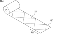
- FIG. 4 is a perspective view schematically showing an example of a process of cutting out a mother sheet from a rolled metal foil.
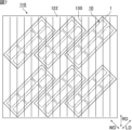
- FIG. 5 is a plan view schematically showing an example of a process for producing a capacitor array assembly.
- FIG. 6 is a perspective view schematically showing another example of the process of cutting out a mother sheet from a rolled metal foil.
- FIG. 7 is a plan view schematically showing another example of the process of fabricating the capacitor array assembly.
- a capacitor array according to the present invention will be described below.
- the present invention is not limited to the following configurations, and can be appropriately modified and applied without changing the gist of the present invention. It should be noted that a combination of two or more of the individual preferred configurations of the invention described below is also the invention.
- terms indicating the relationship between elements e.g., “parallel”, “perpendicular”, “perpendicular”, etc.
- terms indicating the shape of elements are not expressions that express only strict meanings, but substantially It is an expression that means that a difference of approximately several percent is also included, for example, a range equivalent to each other.
- FIG. 1 is a plan view schematically showing one example of the capacitor array of the present invention.
- FIG. 2 is a cross-sectional view of the capacitor array shown in FIG. 1 along line II-II.
- a capacitor array 1 shown in FIG. 1 includes a plurality of capacitor elements 10 .
- Capacitor array 1 has a sheet-like shape as a whole. Although six capacitor elements 10 are shown in FIG. 1, the number of capacitor elements 10 included in the capacitor array 1 is not particularly limited as long as it is two or more. The size, shape, etc. of the capacitor elements 10 may be the same, or may be partially or wholly different.
- each of the plurality of capacitor elements 10 has a porous portion 21A provided on at least one main surface thereof, and includes an anode plate 21 made of a valve metal and a dielectric provided on the surface of the porous portion 21A. and a cathode layer 23 provided on the surface of the dielectric layer 22 and including a solid electrolyte layer 23A.
- Anode plate 21 constituting capacitor element 10 includes, for example, core portion 21B and porous portion 21A provided on at least one main surface of core portion 21B.
- Cathode layer 23 forming capacitor element 10 includes, for example, solid electrolyte layer 23A provided on the surface of dielectric layer 22, and conductor layer 23B provided on the surface of solid electrolyte layer 23A.
- the capacitor array 1 may further include a sealing layer 11 provided to cover the cathode layer 23 forming each capacitor element 10 .
- the capacitor array 1 includes a first external electrode 12 provided outside the sealing layer 11 and electrically connected to the anode plate 21 , and a cathode layer 23 provided outside the sealing layer 11 and electrically connected to the cathode layer 23 . It may further include a second external electrode 13 that is physically connected.
- the form in which the anode plate 21 and the first external electrode 12 are connected is not particularly limited, and they may be connected via via conductors or through-hole conductors.
- the form in which the cathode layer 23 and the second external electrode 13 are connected is not particularly limited, and may be connected via via conductors or through-hole conductors.
- the configurations of the capacitor elements 10 are preferably the same. Moreover, it is preferable that the distance from the surface of sealing layer 11 to anode plate 21 constituting each capacitor element 10 is constant.
- FIG. 3 is a plan view schematically showing a characteristic portion of the capacitor array shown in FIG. 1.
- the anode plate 21 is a rolled metal foil. Specifically, anode plate 21 constituting each capacitor element 10 is formed by cutting out a sheet of rolled metal foil.
- the rolling direction of the anode plate 21 (the direction indicated by the double-headed arrow RD in FIG. neither parallel nor perpendicular to
- the rolling direction RD of the anode plate 21 corresponds to the longitudinal direction of the outer shape of the capacitor array 1 ( , the direction indicated by the double arrow LD), and neither parallel nor perpendicular to the width direction of the outer shape of the capacitor array 1 (the direction indicated by the double arrow WD in FIG. 3).
- a rolled metal foil has different shrinkage behavior when heat is applied in a direction parallel to the rolling direction RD and in a direction perpendicular to the rolling direction RD and parallel to the metal foil.
- the shrinkage behavior of the metal foil forming the anode plate 21 of each capacitor element 10 overlaps with the warpage behavior of the capacitor array 1 as a product, the capacitor A large distortion may occur in the array 1 . Therefore, by shifting the rolling direction RD of the anode plate 21 with respect to each side forming the outer shape of the capacitor array 1, occurrence of large distortion in the capacitor array 1 can be reduced.
- the rolling direction RD (Rolling Direction) of the anode plate 21 means the direction in which the metal foil extends when the metal foil is passed between a pair of rolls and pressed in the metal foil rolling process. As shown in FIG. 3 , linear streaks called rolling marks 30 are formed on the surface of the anode plate 21 in the rolling direction RD of the anode plate 21 . Since the rolling marks 30 extend along the rolling direction RD, the rolling direction RD of the anode plate 21 can be grasped by observing the surface of the anode plate 21 .
- rolling direction RD of anode plate 21 is arranged at an angle of 30° or more and 60° or less with respect to at least one side forming the outer shape of capacitor array 1 . It is more preferably arranged at an angle of 40° or more and 50° or less, and more preferably arranged at an angle of 45° ⁇ 3°. In that case, as shown in FIG. 3, it becomes easier to arrange the plurality of capacitor elements 10 repeatedly and regularly.
- rolling direction RD of anode plate 21 may be arranged at an angle of 30° or more and 60° or less with respect to each side forming the outer shape of capacitor array 1 . , may be arranged at an angle of 40° or more and 50° or less, or may be arranged at an angle of 45° ⁇ 3°.
- each side forming the outer shape of the capacitor element 10 is preferably neither parallel nor perpendicular to the rolling direction RD of the anode plate 21.
- a capacitor element 10 whose sides are parallel or perpendicular to the rolling direction RD of the anode plate 21 may be included.
- the anode plate 21 is made of a valve action metal exhibiting a so-called valve action.
- valve metals include simple metals such as aluminum, tantalum, niobium, titanium, and zirconium, and alloys containing these metals. Among these, aluminum or an aluminum alloy is preferred.
- the anode plate 21 only needs to include the porous portion 21A on at least one main surface, and may include the porous portion 21A on both of the main surfaces.
- Porous portion 21A is preferably an etching layer formed on at least the surface of anode plate 21 .
- the thickness of the anode plate 21 before etching is preferably 60 ⁇ m or more and 200 ⁇ m or less.
- the thickness of the core portion 21B that is not etched after the etching process is preferably 15 ⁇ m or more and 70 ⁇ m or less.
- the thickness of the porous portion 21A is designed according to the required withstand voltage and capacitance.
- the pore diameter of the porous portion 21A is preferably 10 nm or more and 600 nm or less.
- the pore diameter of the porous portion 21A means the median diameter D50 measured by a mercury porosimeter.
- the pore size of the porous portion 21A can be controlled, for example, by adjusting various etching conditions.
- the dielectric layer 22 is provided on the surface of the porous portion 21A.
- the dielectric layer 22 is porous reflecting the surface state of the porous portion 21A, and has a fine uneven surface shape.
- the dielectric layer 22 is preferably made of an oxide film of the valve action metal.
- an aluminum foil is used as the anode plate 21
- the surface of the aluminum foil is anodized (also referred to as chemical conversion treatment) in an aqueous solution containing ammonium adipate or the like to form a dielectric layer made of an oxide film. 22 can be formed.
- the thickness of the dielectric layer 22 is designed according to the required withstand voltage and capacitance, and is preferably 10 nm or more and 100 nm or less.
- the cathode layer 23 is provided on the surface of the dielectric layer 22 .
- Cathode layer 23 includes a solid electrolyte layer 23A provided on the surface of dielectric layer 22 .
- Cathode layer 23 preferably further includes conductor layer 23B provided on the surface of solid electrolyte layer 23A.
- Solid electrolyte layer 23A examples include conductive polymers such as polypyrroles, polythiophenes, and polyanilines. Among these, polythiophenes are preferred, and poly(3,4-ethylenedioxythiophene) called PEDOT is particularly preferred. Moreover, the conductive polymer may contain a dopant such as polystyrene sulfonic acid (PSS).
- Solid electrolyte layer 23 ⁇ /b>A preferably includes an inner layer that fills pores (recesses) of dielectric layer 22 and an outer layer that covers dielectric layer 22 .
- the thickness of the solid electrolyte layer 23A from the surface of the porous portion 21A is preferably 2 ⁇ m or more and 20 ⁇ m or less.
- a polymer film such as poly(3,4-ethylenedioxythiophene) is formed on the surface of the dielectric layer 22 using a treatment liquid containing a monomer such as 3,4-ethylenedioxythiophene. It is formed by a method of forming, a method of applying a dispersion liquid of a polymer such as poly(3,4-ethylenedioxythiophene) to the surface of the dielectric layer 22 and drying it.
- the solid electrolyte layer 23A can be formed in a predetermined region by applying the treatment liquid or dispersion liquid described above onto the dielectric layer 22 by a method such as sponge transfer, screen printing, dispenser coating, or inkjet printing. .
- the conductor layer 23B includes at least one of a conductive resin layer and a metal layer.
- the conductor layer 23B may be only a conductive resin layer or only a metal layer.
- the conductor layer 23B preferably covers the entire surface of the solid electrolyte layer 23A.
- the conductive resin layer examples include a conductive adhesive layer containing at least one conductive filler selected from the group consisting of silver filler, copper filler, nickel filler and carbon filler.
- metal layers include metal plating films and metal foils.
- the metal layer is preferably made of at least one kind of metal selected from the group consisting of nickel, copper, silver and alloys containing these metals as main components.
- the “main component” refers to an elemental component having the largest weight ratio.
- the conductor layer 23B includes, for example, a carbon layer provided on the surface of the solid electrolyte layer 23A and a copper layer provided on the surface of the carbon layer.
- the carbon layer is provided to electrically and mechanically connect the solid electrolyte layer 23A and the copper layer.
- the carbon layer can be formed in a predetermined area by applying carbon paste onto the solid electrolyte layer 23A by a method such as sponge transfer, screen printing, dispenser application, or inkjet printing.
- the thickness of the carbon layer is preferably 2 ⁇ m or more and 20 ⁇ m or less.
- the copper layer can be formed by applying a copper paste onto the carbon layer by a method such as sponge transfer, screen printing, spray coating, dispenser coating, or inkjet printing.
- the thickness of the copper layer is preferably 2 ⁇ m or more and 20 ⁇ m or less.
- the plurality of capacitor elements 10 included in the capacitor array 1 may be arranged linearly or in a plane.
- the plurality of capacitor elements 10 may be arranged regularly or may be arranged irregularly.
- the size, planar shape, and the like of capacitor element 10 viewed in the thickness direction may be the same, or may be partially or wholly different.
- the capacitor array 1 may include two or more types of capacitor elements 10 having different capacitive part areas when viewed in the thickness direction.
- the capacitor array 1 may include a capacitor element 10 whose planar shape of the capacitor section when viewed in the thickness direction is not rectangular.
- "rectangular" means square or rectangular. Therefore, for example, the plane shape of the capacitor element 10 may include polygons other than rectangles such as squares, triangles, pentagons, and hexagons, shapes including curved portions, circles, ellipses, and the like. . In this case, two or more types of capacitor elements 10 having different planar shapes of the capacitive portions may be included. Further, in addition to the capacitor element 10 whose capacity part has a non-rectangular planar shape, the capacitor element 10 whose capacity part has a rectangular planar shape may or may not be included.
- At least one pair of adjacent capacitor elements 10 may be divided by slits.
- the slits divide anode plate 21 between adjacent capacitor elements 10 .
- the inside of the slit may be filled with the sealing layer 11 . Sealing layer 11 reliably separates anode plate 21 between adjacent capacitor elements 10 .
- Anode plates 21 may be physically separated by slits between adjacent capacitor elements 10, or may be separated electrically.
- the width of the slits is not particularly limited, but is preferably 15 ⁇ m or more, more preferably 30 ⁇ m or more, and even more preferably 50 ⁇ m or more.
- the width of the slit is preferably 500 ⁇ m or less, more preferably 200 ⁇ m or less, even more preferably 150 ⁇ m or less.
- the slit may have a taper that decreases in width in the thickness direction.
- At least part of the slit may be arranged so as not to cover the entire capacitor array 1 .
- at least one capacitor element 10 may be arranged on the extension of the slit.
- the sealing layer 11 is provided so as to cover the cathode layer 23 forming each capacitor element 10 .
- Sealing layer 11 may be provided so as to cover both main surface sides of anode plate 21, or may be provided so as to cover either one main surface side.
- the sealing layer 11 is preferably made of resin.
- the resin forming the sealing layer 11 include epoxy resin and phenol resin.
- the sealing layer 11 preferably contains a filler.
- fillers contained in the sealing layer 11 include inorganic fillers such as silica particles, alumina particles, and metal particles.
- the sealing layer 11 may be composed of only one layer, or may be composed of two or more layers. When the sealing layer 11 is composed of two or more layers, the materials forming each sealing layer may be the same or different.
- layers such as a stress relaxation layer and a moisture-proof film may be provided.
- An insulating layer for insulating the anode plate 21 and the cathode layer 23 may be provided on the surface of the dielectric layer 22 where the cathode layer 23 is not provided.
- the insulating layer is preferably made of resin.
- the resin constituting the insulating layer include polyphenylsulfone resin, polyethersulfone resin, cyanate ester resin, fluorine resin (tetrafluoroethylene, tetrafluoroethylene-perfluoroalkyl vinyl ether copolymer, etc.), polyimide resin, Examples include insulating resins such as polyamideimide resins, epoxy resins, and derivatives or precursors thereof.
- the insulating layer may be composed of the same resin as the sealing layer 11 . Unlike the sealing layer 11, if the insulating layer contains an inorganic filler, the effective portion of the capacitor element 10 may be adversely affected.
- the insulating layer can be formed, for example, by applying a mask material such as a composition containing an insulating resin onto the dielectric layer 22 by a method such as sponge transfer, screen printing, dispenser coating, or inkjet printing.
- a mask material such as a composition containing an insulating resin
- the capacitor array 1 may include through-hole conductors provided inside the through-holes.
- the cross-sectional shape of the through-hole when viewed in the thickness direction is not particularly limited, and may be, for example, a polygonal shape such as a square, a circular shape, an elliptical shape, or the like.
- the pore diameter means the diameter when the cross-sectional shape is circular, and the maximum length passing through the center of the cross-section when the cross-sectional shape is not circular.
- the through-hole may have a taper in which the hole diameter becomes smaller in the thickness direction.
- the through-hole conductor should be provided at least on the inner wall surface of the through-hole.
- the inner wall surface of the through-hole is metallized with a low resistance metal such as copper, gold or silver. For ease of processing, it can be metallized by, for example, electroless copper plating, electrolytic copper plating, or the like.
- the metallization of the through-hole conductor is not limited to the case of metallizing only the inner wall surface of the through-hole, and the through-hole may be filled with a metal or a composite material of metal and resin.
- the through-hole conductor is A. for capacitor anode; B. for capacitor cathode and ground, C.I. for I/O lines.
- a through-hole conductor for the anode of the capacitor is electrically connected to the anode plate 21;B.
- the through-hole conductors for the capacitor cathode and ground are electrically connected to the cathode layer 23; Through-hole conductors for I/O lines are not electrically connected to either anode plate 21 or cathode layer 23 .
- the through-hole conductor for the anode of the capacitor may or may not be filled with an insulating material between the through-hole and the through-hole conductor.
- the capacitor array of the present invention can preferably be manufactured by the following method.
- the method for manufacturing a capacitor array of the present invention comprises: a step of cutting out a mother sheet from the rolled metal foil; a step of fabricating a capacitor array assembly in which a plurality of capacitor arrays are arranged on the mother sheet; and cutting the capacitor array assembly into individual capacitor arrays.
- FIG. 4 is a perspective view schematically showing an example of a process of cutting out a mother sheet from a rolled metal foil.
- a mother sheet 121 is cut out from a rolled metal foil 120 at an angle to the rolling direction (the direction indicated by the double arrow RD in FIG. 4).
- the angle of at least one side of the mother sheet 121 with respect to the rolling direction RD is preferably 30° or more and 60° or less, more preferably 40° or more and 50° or less, and even more preferably 45° ⁇ 3°.
- the angle of each side of the mother sheet 121 with respect to the rolling direction RD may be 30° or more and 60° or less, may be 40° or more and 50° or less, or may be 45° ⁇ 3°.
- the porous portion 21A (see FIG. 2) is formed on at least one main surface of the mother sheet 121, and the dielectric layer 22 (see FIG. 2) is formed on the surface of the porous portion 21A.
- the dielectric layer 22 is formed on the surface of the porous portion 21A.
- the surface of the aluminum foil is etched to form the porous portion 21A, and then anodized in an aqueous solution containing ammonium adipate or the like.
- a dielectric layer 22 made of an oxide film is formed.
- a chemically processed foil of aluminum or the like may be prepared as the mother sheet 121 having the porous portion 21A provided on at least one main surface and the dielectric layer 22 provided on the surface of the porous portion 21A.
- FIG. 5 is a plan view schematically showing an example of a process for producing a capacitor array assembly.
- capacitor array assembly 100 in which a plurality of capacitor arrays 1 are arranged on a common mother sheet 121 is manufactured.
- Capacitor array assembly 100 has a sheet-like shape as a whole. Although eight capacitor arrays 1 are shown in FIG. 5, the number of capacitor arrays 1 included in capacitor array assembly 100 is not particularly limited as long as it is two or more. The size, shape, etc. of the capacitor arrays 1 may be the same, or part or all of them may be different.
- a plurality of capacitor arrays 1 each include a plurality of capacitor elements 10 (see FIGS. 1 and 2).
- the cathode layer 23 is formed on the surface of the dielectric layer 22 of the mother sheet 121 .
- a solid electrolyte layer 23 A (see FIG. 2) is formed on the surface of the dielectric layer 22 of the mother sheet 121 .
- a conductor layer 23B (see FIG. 2) on the surface of the solid electrolyte layer 23A.
- the capacitor element 10 in which the anode plate 21 (see FIG. 2) is composed of the mother sheet 121 can be produced.
- an insulating layer may be formed on the surface of the dielectric layer 22 in order to divide the effective portion of the capacitor element 10 .
- the mother sheet 121 is formed by cutting out the rolled metal foil 120 at an angle to the rolling direction RD. Therefore, as shown in FIG. 5, in a plan view of the mother sheet 121 in the thickness direction, the rolling direction of the mother sheet 121 (the direction indicated by the double arrow RD in FIG. 5) constitutes the outer shape of the mother sheet 121. Neither parallel nor perpendicular to each side.
- the rolling direction RD of the mother sheet 121 corresponds to the longitudinal direction of the outer shape of the mother sheet 121 (in FIG. left-right direction), and neither parallel nor perpendicular to the width direction (vertical direction in FIG. 5) of the outer shape of the mother sheet 121 .
- the rolling direction RD of the mother sheet 121 is neither parallel nor perpendicular to the sides forming the outer shape of the capacitor array 1 in a plan view in the thickness direction of the mother sheet 121. .
- FIG. 5 shows that as shown in FIG.
- the rolling direction RD of the mother sheet 121 corresponds to the longitudinal direction of the outer shape of the capacitor array 1 ( , the direction indicated by the double arrow LD), and neither parallel nor perpendicular to the width direction of the outer shape of the capacitor array 1 (the direction indicated by the double arrow WD in FIG. 5).
- linear streaks called rolling marks 130 are formed on the surface of the mother sheet 121 in the rolling direction RD of the mother sheet 121 . Since the rolling marks 130 extend along the rolling direction RD, the rolling direction RD of the mother sheet 121 can be grasped by observing the surface of the mother sheet 121 .
- the rolling direction RD of the mother sheet 121 is arranged at an angle of 30° or more and 60° or less with respect to at least one side forming the outer shape of the capacitor array 1. It is more preferably arranged at an angle of 40° or more and 50° or less, and more preferably arranged at an angle of 45° ⁇ 3°.
- the rolling direction RD of the mother sheet 121 may be arranged at an angle of 30° or more and 60° or less with respect to each side forming the outer shape of the capacitor array 1. , may be arranged at an angle of 40° or more and 50° or less, or may be arranged at an angle of 45° ⁇ 3°.
- each side forming the outer shape of the mother sheet 121 is parallel or perpendicular to at least one side forming the outer shape of the capacitor array 1. More preferably, it is parallel or perpendicular to each side forming the outer shape of the capacitor array 1 .
- each side forming the outer shape of the capacitor element 10 is preferably neither parallel nor perpendicular to the rolling direction RD of the mother sheet 121.
- Capacitor elements 10 whose sides are parallel or perpendicular to the rolling direction RD of the mother sheet 121 may be included.
- FIG. 6 is a perspective view schematically showing another example of the process of cutting out a mother sheet from a rolled metal foil.
- a mother sheet 122 is cut out from a rolled metal foil 120 parallel or perpendicular to the rolling direction (the direction indicated by the double arrow RD in FIG. 6).
- the porous portion 21A (see FIG. 2) is formed on at least one main surface of the mother sheet 122, and the dielectric layer 22 (see FIG. 2) is formed on the surface of the porous portion 21A.
- a chemically processed foil such as aluminum may be prepared as the mother sheet 122 having the porous portion 21A provided on at least one main surface and the dielectric layer 22 provided on the surface of the porous portion 21A.
- FIG. 7 is a plan view schematically showing another example of the process of producing a capacitor array assembly.
- capacitor array assembly 110 in which a plurality of capacitor arrays 1 are arranged on a common mother sheet 122 is produced.
- Capacitor array assembly 110 has a sheet-like shape as a whole. Although six capacitor arrays 1 are shown in FIG. 7, the number of capacitor arrays 1 included in capacitor array assembly 110 is not particularly limited as long as it is two or more. The size, shape, etc. of the capacitor arrays 1 may be the same, or part or all of them may be different.
- a plurality of capacitor arrays 1 each include a plurality of capacitor elements 10 (see FIGS. 1 and 2).
- the cathode layer 23 is formed on the surface of the dielectric layer 22 of the mother sheet 122 .
- a solid electrolyte layer 23 A (see FIG. 2) is formed on the surface of the dielectric layer 22 of the mother sheet 122 .
- a conductor layer 23B (see FIG. 2) on the surface of the solid electrolyte layer 23A.
- the capacitor element 10 in which the anode plate 21 (see FIG. 2) is composed of the mother sheet 122 can be produced.
- an insulating layer may be formed on the surface of the dielectric layer 22 in order to divide the effective portion of the capacitor element 10 .
- the mother sheet 122 is formed by cutting out the rolled metal foil 120 parallel or perpendicular to the rolling direction RD. Therefore, as shown in FIG. 7, in a plan view of the mother sheet 122 in the thickness direction, the rolling direction of the mother sheet 122 (the direction indicated by the double arrow RD in FIG. 7) constitutes the outer shape of the mother sheet 122. It is preferably parallel or perpendicular to at least one side, and more preferably parallel or perpendicular to each side forming the outer shape of the mother sheet 122 . For example, as shown in FIG.
- the rolling direction RD of the mother sheet 122 corresponds to the longitudinal direction of the outer shape of the mother sheet 122 (in FIG. lateral direction) and parallel to the width direction (vertical direction in FIG. 7) of the outer shape of the mother sheet 122 .
- the multiple capacitor arrays 1 are arranged at an angle to the rolling direction RD of the mother sheet 122 .
- the rolling direction RD of the mother sheet 122 is neither parallel nor perpendicular to the sides forming the outer shape of the capacitor array 1 in a plan view in the thickness direction of the mother sheet 122. .
- FIG. 7 shows that as shown in FIG.
- the rolling direction RD of the mother sheet 122 corresponds to the longitudinal direction of the outer shape of the capacitor array 1 ( , the direction indicated by the double-headed arrow LD), and neither parallel nor perpendicular to the width direction of the outer shape of the capacitor array 1 (the direction indicated by the double-headed arrow WD in FIG. 7).
- the method shown in FIG. 7 is more advantageous in processing when manufacturing the capacitor array 1 than the method shown in FIG.
- the effective portion of the capacitor element 10 is formed by screen printing, the sides of the squeegee and the sides forming the outer shape of the capacitor array 1 do not overlap in parallel, which stabilizes the processing.
- linear streaks called rolling marks 130 are formed on the surface of the mother sheet 122 in the rolling direction RD of the mother sheet 122 . Since the rolling marks 130 extend along the rolling direction RD, the rolling direction RD of the mother sheet 122 can be grasped by observing the surface of the mother sheet 122 .
- the rolling direction RD of the mother sheet 122 is arranged at an angle of 30° or more and 60° or less with respect to at least one side forming the outer shape of the capacitor array 1. It is more preferably arranged at an angle of 40° or more and 50° or less, and more preferably arranged at an angle of 45° ⁇ 3°.
- the rolling direction RD of the mother sheet 122 may be arranged at an angle of 30° or more and 60° or less with respect to each side forming the outer shape of the capacitor array 1. , may be arranged at an angle of 40° or more and 50° or less, or may be arranged at an angle of 45° ⁇ 3°.
- the sides forming the contour of the mother sheet 122 are neither parallel nor perpendicular to the sides forming the contour of the capacitor array 1. is preferred.
- each side forming the outer shape of the mother sheet 122 is arranged at an angle of 30° or more and 60° or less with respect to at least one side forming the outer shape of the capacitor array 1 . more preferably at an angle of 40° or more and 50° or less, and even more preferably at an angle of 45° ⁇ 3°.
- each side forming the outer shape of the mother sheet 122 is arranged at an angle of 30° or more and 60° or less with respect to each side forming the outer shape of the capacitor array 1 . may be arranged at an angle of 40° or more and 50° or less, or may be arranged at an angle of 45° ⁇ 3°.
- each side forming the outer shape of the capacitor element 10 is preferably neither parallel nor perpendicular to the rolling direction RD of the mother sheet 122.
- Capacitor elements 10 whose sides are parallel or perpendicular to the rolling direction RD of the mother sheet 122 may be included.
- the sealing layer 11 may be formed so as to cover the cathode layer 23 constituting each capacitor element 10.
- the sealing layer 11 can be formed so as to cover both main surfaces of the mother sheet 121 or 122 or any one of the main surfaces thereof.
- a first external electrode 12 (see FIGS. 1 and 2) electrically connected to the anode plate 21 and a second external electrode 13 (see FIGS. 1 and 2) electrically connected to the cathode layer 23 are provided. 1 and 2) may be further formed.
- a through-hole conductor extending in the thickness direction may be formed inside the through-hole.
- methods for forming through holes include laser processing and dicing processing.
- slits may be formed between the capacitor elements 10 .
- methods for forming slits include laser processing and dicing processing.
- the capacitor array assembly 100 or 110 can be cut into individual capacitor arrays 1 .
- a method such as dicing is used to cut the capacitor array assembly 100 or 110 .
- the capacitor array 1 can be manufactured.
- the capacitor array of the present invention can be suitably used as a constituent material for composite electronic components.
- a composite electronic component is provided, for example, on the capacitor array of the present invention and on the outside of the capacitor array (preferably outside the sealing layer of the capacitor array), and the anode plate and the cathode layer of the capacitor array.
- An external electrode electrically connected to each, and an electronic component connected to the external electrode.
- the electronic component connected to the external electrode may be either a passive element or an active element. Both the passive element and the active element may be connected to the external electrode, or either one of the passive element and the active element may be connected to the external electrode. Also, composites of passive and active elements may be connected to external electrodes.
- Passive elements include, for example, inductors. Active elements include memories, GPUs (Graphical Processing Units), CPUs (Central Processing Units), MPUs (Micro Processing Units), PMICs (Power Management ICs), and the like.
- the capacitor array of the present invention has a sheet-like shape as a whole. Therefore, in the composite electronic component, the capacitor array can be treated like a mounting substrate, and the electronic component can be mounted on the capacitor array. Furthermore, by making the electronic components mounted on the capacitor array sheet-shaped, it is possible to connect the capacitor array and electronic components in the thickness direction via through-hole conductors that pass through each electronic component in the thickness direction. is. As a result, active elements and passive elements can be configured as a single module.
- a switching regulator can be formed by electrically connecting the capacitor array of the present invention between a voltage regulator including a semiconductor active element and a load to which the converted DC voltage is supplied.
- a circuit layer may be formed on one side of a capacitor matrix sheet in which a plurality of capacitor arrays of the present invention are further laid out, and then connected to a passive element or an active element.
- the capacitor array assembly may be used as a capacitor matrix sheet.
- the capacitor array of the present invention may be placed in a cavity provided in advance on a substrate, embedded with resin, and then the circuit layer may be formed on the resin.
- Another electronic component passive element or active element
- the capacitor array of the present invention may be mounted on a smooth carrier such as a wafer or glass, and after forming an outer layer portion with resin, forming a circuit layer, and then connecting to a passive element or an active element. good.
- capacitor array 10 capacitor element 11 sealing layer 12 first external electrode 13 second external electrode 21 anode plate 21A porous portion 21B core portion 22 dielectric layer 23 cathode layer 23A solid electrolyte layer 23B conductor layer 30, 130 rolling marks 100, 110 Capacitor array assembly 120 Rolled metal foil 121, 122 Mother sheet RD Rolling direction LD Longitudinal direction of capacitor array outline WD Width direction of capacitor array outline
Landscapes
- Engineering & Computer Science (AREA)
- Power Engineering (AREA)
- Microelectronics & Electronic Packaging (AREA)
- Manufacturing & Machinery (AREA)
- Fixed Capacitors And Capacitor Manufacturing Machines (AREA)
Priority Applications (2)
| Application Number | Priority Date | Filing Date | Title |
|---|---|---|---|
| CN202290000199.6U CN219998063U (zh) | 2021-09-06 | 2022-08-16 | 电容器阵列以及电容器阵列集合体 |
| JP2023513712A JP7294563B1 (ja) | 2021-09-06 | 2022-08-16 | コンデンサアレイ及びコンデンサアレイ集合体 |
Applications Claiming Priority (2)
| Application Number | Priority Date | Filing Date | Title |
|---|---|---|---|
| JP2021-144863 | 2021-09-06 | ||
| JP2021144863 | 2021-09-06 |
Publications (1)
| Publication Number | Publication Date |
|---|---|
| WO2023032657A1 true WO2023032657A1 (ja) | 2023-03-09 |
Family
ID=85411056
Family Applications (1)
| Application Number | Title | Priority Date | Filing Date |
|---|---|---|---|
| PCT/JP2022/030958 Ceased WO2023032657A1 (ja) | 2021-09-06 | 2022-08-16 | コンデンサアレイ及びコンデンサアレイ集合体 |
Country Status (3)
| Country | Link |
|---|---|
| JP (1) | JP7294563B1 (https=) |
| CN (1) | CN219998063U (https=) |
| WO (1) | WO2023032657A1 (https=) |
Citations (4)
| Publication number | Priority date | Publication date | Assignee | Title |
|---|---|---|---|---|
| JPS63160805A (ja) * | 1986-11-11 | 1988-07-04 | アルカン・インターナショナル・リミテッド | 陽極酸化アルミニウムシートの成形方法 |
| JPH06314638A (ja) * | 1993-04-28 | 1994-11-08 | Showa Alum Corp | 電解コンデンサ電極用アルミニウム箔 |
| JP2002261179A (ja) * | 2001-02-27 | 2002-09-13 | Kyocera Corp | 電子部品収納用パッケージ |
| WO2019239937A1 (ja) * | 2018-06-11 | 2019-12-19 | 株式会社村田製作所 | コンデンサアレイ、複合電子部品、コンデンサアレイの製造方法、及び、複合電子部品の製造方法 |
-
2022
- 2022-08-16 JP JP2023513712A patent/JP7294563B1/ja active Active
- 2022-08-16 CN CN202290000199.6U patent/CN219998063U/zh active Active
- 2022-08-16 WO PCT/JP2022/030958 patent/WO2023032657A1/ja not_active Ceased
Patent Citations (4)
| Publication number | Priority date | Publication date | Assignee | Title |
|---|---|---|---|---|
| JPS63160805A (ja) * | 1986-11-11 | 1988-07-04 | アルカン・インターナショナル・リミテッド | 陽極酸化アルミニウムシートの成形方法 |
| JPH06314638A (ja) * | 1993-04-28 | 1994-11-08 | Showa Alum Corp | 電解コンデンサ電極用アルミニウム箔 |
| JP2002261179A (ja) * | 2001-02-27 | 2002-09-13 | Kyocera Corp | 電子部品収納用パッケージ |
| WO2019239937A1 (ja) * | 2018-06-11 | 2019-12-19 | 株式会社村田製作所 | コンデンサアレイ、複合電子部品、コンデンサアレイの製造方法、及び、複合電子部品の製造方法 |
Also Published As
| Publication number | Publication date |
|---|---|
| CN219998063U (zh) | 2023-11-10 |
| JP7294563B1 (ja) | 2023-06-20 |
| JPWO2023032657A1 (https=) | 2023-03-09 |
Similar Documents
| Publication | Publication Date | Title |
|---|---|---|
| JP7574840B2 (ja) | コンデンサ及び複合電子部品 | |
| US11232912B2 (en) | Solid electrolytic capacitor | |
| TWI829265B (zh) | 電容器元件 | |
| WO2023054059A1 (ja) | コンデンサ素子、モジュール及び半導体複合装置 | |
| JP2023122337A (ja) | 固体電解コンデンサの製造方法、コンデンサアレイの製造方法、固体電解コンデンサ及びコンデンサアレイ | |
| US20250125098A1 (en) | Capacitor element | |
| WO2023218801A1 (ja) | コンデンサ | |
| WO2024070531A1 (ja) | コンデンサ素子 | |
| US20250079090A1 (en) | Solid electrolytic capacitor and capacitor array | |
| US20250273405A1 (en) | Capacitor element | |
| JP7619540B1 (ja) | コンデンサ素子 | |
| JP7294563B1 (ja) | コンデンサアレイ及びコンデンサアレイ集合体 | |
| WO2024190398A1 (ja) | コンデンサ素子 | |
| WO2024070529A1 (ja) | コンデンサ素子 | |
| JP7722616B2 (ja) | コンデンサアレイ | |
| JP7622919B1 (ja) | コンデンサ素子製造用基板及びコンデンサ素子の製造方法 | |
| US20250201486A1 (en) | Capacitor embedded substrate | |
| WO2025069676A1 (ja) | コンデンサ素子 | |
| WO2026048932A1 (ja) | コンデンサ素子 | |
| WO2025243714A1 (ja) | コンデンサ素子 | |
| WO2026048931A1 (ja) | コンデンサ素子 | |
| WO2026048924A1 (ja) | コンデンサ素子 | |
| WO2024247589A1 (ja) | コンデンサ素子 | |
| WO2026048937A1 (ja) | コンデンサ素子 | |
| WO2026048925A1 (ja) | コンデンサ素子 |
Legal Events
| Date | Code | Title | Description |
|---|---|---|---|
| ENP | Entry into the national phase |
Ref document number: 2023513712 Country of ref document: JP Kind code of ref document: A |
|
| WWE | Wipo information: entry into national phase |
Ref document number: 202290000199.6 Country of ref document: CN |
|
| 121 | Ep: the epo has been informed by wipo that ep was designated in this application |
Ref document number: 22864242 Country of ref document: EP Kind code of ref document: A1 |
|
| NENP | Non-entry into the national phase |
Ref country code: DE |
|
| 122 | Ep: pct application non-entry in european phase |
Ref document number: 22864242 Country of ref document: EP Kind code of ref document: A1 |