WO2023032511A1 - アンテナ装置、および通信端末装置 - Google Patents
アンテナ装置、および通信端末装置 Download PDFInfo
- Publication number
- WO2023032511A1 WO2023032511A1 PCT/JP2022/028381 JP2022028381W WO2023032511A1 WO 2023032511 A1 WO2023032511 A1 WO 2023032511A1 JP 2022028381 W JP2022028381 W JP 2022028381W WO 2023032511 A1 WO2023032511 A1 WO 2023032511A1
- Authority
- WO
- WIPO (PCT)
- Prior art keywords
- antenna
- coil
- antenna device
- impedance
- ant2
- Prior art date
- Legal status (The legal status is an assumption and is not a legal conclusion. Google has not performed a legal analysis and makes no representation as to the accuracy of the status listed.)
- Ceased
Links
Images







Classifications
-
- H—ELECTRICITY
- H01—ELECTRIC ELEMENTS
- H01Q—ANTENNAS, i.e. RADIO AERIALS
- H01Q1/00—Details of, or arrangements associated with, antennas
- H01Q1/12—Supports; Mounting means
- H01Q1/22—Supports; Mounting means by structural association with other equipment or articles
- H01Q1/24—Supports; Mounting means by structural association with other equipment or articles with receiving set
- H01Q1/241—Supports; Mounting means by structural association with other equipment or articles with receiving set used in mobile communications, e.g. GSM
- H01Q1/242—Supports; Mounting means by structural association with other equipment or articles with receiving set used in mobile communications, e.g. GSM specially adapted for hand-held use
- H01Q1/243—Supports; Mounting means by structural association with other equipment or articles with receiving set used in mobile communications, e.g. GSM specially adapted for hand-held use with built-in antennas
-
- H—ELECTRICITY
- H01—ELECTRIC ELEMENTS
- H01Q—ANTENNAS, i.e. RADIO AERIALS
- H01Q5/00—Arrangements for simultaneous operation of antennas on two or more different wavebands, e.g. dual-band or multi-band arrangements
- H01Q5/30—Arrangements for providing operation on different wavebands
- H01Q5/378—Combination of fed elements with parasitic elements
-
- H—ELECTRICITY
- H03—ELECTRONIC CIRCUITRY
- H03H—IMPEDANCE NETWORKS, e.g. RESONANT CIRCUITS; RESONATORS
- H03H7/00—Multiple-port networks comprising only passive electrical elements as network components
- H03H7/38—Impedance-matching networks
Definitions
- the present disclosure relates to technology of antenna devices and communication terminal devices.
- Patent Document 1 discloses an antenna device in which two antennas, a fed antenna and a parasitic antenna, are coupled.
- the resonance frequency is not so high, so the length of the antenna is sufficient (the length of the radiating element) can be ensured.
- the length of the antenna becomes shorter as the resonance frequency becomes higher. Therefore, for example, when used in the frequency band (3.3 to 5.0 GHz) used in the 5th generation mobile communication system (5G), the antenna device has a short parasitic antenna length and sufficient radiation efficiency. could not be obtained.
- the present disclosure has been made to solve such problems, and its object is to provide an antenna device and a communication terminal device that can obtain sufficient radiation efficiency while widening the frequency band to be used. be.
- An antenna device is an antenna device comprising a first antenna and a second antenna.
- the first antenna includes a first radiating element connected to a feeding circuit that supplies a high frequency signal, and a first coil connected between the first antenna and the feeding circuit.
- the second antenna includes a second coil magnetically coupled to the first coil and a second radiating element connected to the second coil.
- the impedance of the first antenna is greater than 50 ⁇ at the resonant frequency of the fundamental wave of the second antenna.
- a communication terminal device includes a feeding circuit and the antenna device described above.
- the impedance of the first antenna is greater than 50 ⁇ at the resonance frequency of the fundamental wave of the second antenna, the frequency band to be used can be widened and sufficient radiation efficiency can be obtained. be done.
- FIG. 1 is a circuit diagram of an antenna device according to an embodiment;
- FIG. 1 is a schematic diagram showing a communication terminal device in an embodiment;
- FIG. It is a schematic diagram showing a configuration for measuring the impedance of the first antenna in the embodiment.
- It is a schematic diagram showing a configuration for measuring the impedance of the second antenna in the embodiment.
- It is a figure which shows the frequency characteristic of the reflection coefficient of the antenna device in embodiment.
- It is a figure which shows the Smith chart at the time of adjusting the impedance of the antenna device in embodiment to a 1st state.
- FIG. 10 is a circuit diagram of an antenna device according to Modification 1;
- FIG. 11 is a circuit diagram of an antenna device in Modification 2;
- FIG. 11 is a circuit diagram of an antenna device in Modification 3;
- FIG. 11 is a circuit diagram of an antenna device in Modification 4;
- FIG. 11 is a circuit diagram of an antenna device in Modification 5;
- FIG. 1 is a circuit diagram of an antenna device 100 according to an embodiment.
- the antenna device 100 includes a first antenna ANT1 and a second antenna ANT2.
- the first antenna ANT1 includes a first radiating element 11 connected to the feeding circuit 30 and a first coil L1 connected between the first radiating element 11 and the feeding circuit.
- the second antenna ANT2 includes a second coil L2 magnetically coupled to the first coil L1, and a second radiation element 12 connected to the second coil L2. Therefore, the first antenna ANT1 is a fed antenna that is fed by the feeding circuit 30, and the second antenna ANT2 is not connected to the feeding circuit 30 and is a parasitic antenna that is not fed by the feeding circuit 30.
- a first antenna ANT1 to which power is supplied is provided with a capacitor 13 connected in series and a coil 14 to which one end is connected. The other end of the coil 14 is connected to GND.
- a capacitor 13 and a coil 14 form an LC circuit and function as a filter circuit for the first antenna ANT1. Note that if the filter circuit is unnecessary in the first antenna ANT1, the capacitor 13 and the coil 14 need not be provided.
- the first antenna ANT1 and the second antenna ANT2 are magnetically coupled by the first coil L1 and the second coil L2 in order to widen the usable frequency band. That is, the first coil L1 and the second coil L2 constitute the antenna coupling element 20. As shown in FIG.
- the antenna coupling element 20 is a rectangular parallelepiped chip part mounted on a circuit board in an electronic device.
- the antenna coupling element 20 uses a liquid crystal polymer (LCP [Liquid Crystal Polymer]) sheet as the insulating base material, and copper foil is used to form the first coil L1 and the second coil L1. It is constructed by laminating each insulating base material on which the conductor pattern of the coil L2 is patterned.
- LCP Liquid Crystal Polymer
- the antenna coupling element 20 when the antenna coupling element 20 is composed of a ceramic multilayer substrate, the antenna coupling element 20 uses low temperature co-fired ceramics (LTCC [Low Temperature Co-fired Ceramics]) for the insulating base material, and copper paste is printed. It is configured by laminating respective insulating base materials formed and patterned with conductor patterns of the first coil L1 and the second coil L2. Furthermore, the antenna coupling element 20 is not limited to the ceramic multilayer substrate, and may be formed by, for example, repeatedly applying an insulating paste containing glass as a main component by screen printing. As described above, the antenna coupling element 20 can be used as a transformer with a predetermined inductance and a predetermined coupling coefficient because the insulating base material is non-magnetic (not magnetic ferrite).
- LTCC Low Temperature Co-fired Ceramics
- the antenna device 100 can cover a wide band by connecting two radiation elements (the first radiation element 11 and the second radiation element 12) to the antenna coupling element 20.
- the antenna device 100 covers the frequency band (3.3 to 5.0 GHz) used in the fifth generation mobile communication system (5G) or the frequency band such as the 5 GHz band wireless LAN
- the second antenna ANT2 is required to resonate at a high resonance frequency, and the length of the second radiating element 12 is shortened.
- the length of the second radiation element 12 is shortened, sufficient radiation efficiency may not be obtained.
- the length of the second radiation element 12 can be lengthened by resonating the second antenna ANT2 not at the resonant frequency of the fundamental wave but at the resonant frequency of the harmonic wave. That is, when the resonance frequency to be resonated in the second antenna ANT2 is, for example, 4.4 GHz, the length of the second radiation element 12 is shortened when the second antenna ANT2 is resonated with the fundamental wave of 4.4 GHz. However, when resonating the second antenna ANT2 with the triple harmonic of 4.4 GHz, the resonance frequency of the fundamental wave is 1.4 GHz.
- the length of the radiating element 12 By defining the length of the second radiating element 12 with the resonant frequency of the fundamental wave of 1.4 GHz, the length of the radiating element can be made longer than when the length of the second radiating element 12 is defined with the resonant frequency of the fundamental wave of 4.4 GHz. can.
- the length of the second radiation element 12 is lengthened by causing the second antenna ANT2 to resonate at the resonant frequency of the harmonic, and sufficient radiation efficiency can be obtained.
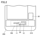
- FIG. 2 is a schematic diagram showing a communication terminal device according to the embodiment.
- the communication terminal device shown in FIG. 2 is a mobile terminal 200 capable of communication in a band including n78 (3.3-3.8 GHz) and a band including n79 (4.4-4.9 GHz). Therefore, mobile terminal 200 is provided with antenna device 100 including first antenna ANT1 excited in a band including n78 and second antenna ANT2 excited in a band including n79.
- the mobile terminal 200 is, for example, a mobile phone, a smart phone, a tablet, or the like.
- the antenna device 100 has an antenna coupling element 20 provided on the back side of a substrate 210 on which the first radiation element 11 and the second radiation element 12 are patterned, and couples the first antenna ANT1 and the second antenna ANT2. Also, although the first antenna ANT1 is electrically connected to the feeding circuit 30 by wiring (not shown), the second antenna ANT2 is not electrically connected to the feeding circuit 30. FIG.
- the first radiation element 11 is composed of a linear conductor pattern extending from the antenna coupling element 20 in the left direction in the drawing.
- the second radiating element 12 is composed of a linear conductor pattern that extends from the antenna coupling element 20 in the right direction in the drawing and turns back in the left direction in the middle. Both the first radiating element 11 and the second radiating element 12 act as a monopole antenna.
- the first antenna ANT1 is excited in a band including n78, and the second antenna ANT2 is excited in a band including n79.
- First radiating element 11 is longer than 12 .
- the second antenna ANT2 resonates at the third harmonic resonance frequency, the length of the radiation element is longer in the second radiation element 12 than in the first radiation element 11, as shown in FIG. there is
- the second antenna ANT2 is resonated at the fundamental resonance frequency.
- the resonance frequency of the fundamental wave of the second antenna ANT2 is not included in the frequency band targeted by the antenna device 100, and the second antenna ANT2 resonates at the resonance frequency of the fundamental wave, the antenna device 100 Interfering waves outside the frequency band are received, and communication performance deteriorates.
- the antenna device 100 adjusts the impedance so as not to resonate at the resonance frequency of the fundamental wave of the second antenna ANT2. Specifically, the antenna device 100 adjusts the impedance of the first antenna ANT1 to be, for example, greater than 50 ⁇ at the resonance frequency of the fundamental wave of the second antenna ANT2.
- the figure of 50 ⁇ is a reference value that is also used in general antenna design, and if the impedance is higher than this, the current flowing through the circuit will decrease. Further, in a general antenna design, the impedance on the input side of the feeding circuit 30 also corresponds to around 50 ⁇ .
- the case where "the target impedance is greater than 50 ⁇ " corresponds to the case where "the target impedance is greater than the impedance on the input side of the feeding circuit 30". Also, in this specification, the magnitude of impedance is compared with an absolute value that takes into consideration the real part and the imaginary part of impedance.
- FIG. 3 is a schematic diagram showing the configuration for measuring the impedance of the first antenna ANT1 according to the embodiment.
- the impedance of the first antenna ANT1 is measured by connecting the network analyzer 50 with the measurement cable 51 to the first coil L1 instead of the feeding circuit 30 as shown in FIG.
- the second radiation element 12 and GND are removed from the second coil L2 to open both ends of the second coil L2.
- the frequency characteristic of the impedance of the first antenna ANT1 is measured by the network analyzer 50 with the connection point between the first coil L1 and the measurement cable 51 as the measurement point t1.
- the phase shift due to the length of the measurement cable 51 is calibrated in advance at the connection point with the first coil L1 on the primary side of the transformer.
- FIG. 4 is a schematic diagram showing a configuration for measuring the impedance of the second antenna ANT2 in the embodiment. Measurement of the resonance frequency of the fundamental wave of the second antenna ANT2 is performed in the second measurement state by connecting the network analyzer 50 to the second coil L2 with the measurement cable 52 instead of connecting to GND as shown in FIG. . At this time, if the first coil L1 and the second coil L2 are integrally formed as an element and it is difficult to separate them, the first radiation element 11 and the feeding circuit 30 are removed from the first coil L1, and both ends of the first coil L1 are opened.
- the frequency characteristic of the fundamental wave of the second antenna ANT2 is measured by the network analyzer 50 with the connection point between the second coil L2 and the measurement cable 52 as the measurement point t2. This measurement allows the resonance frequency of the parasitic element to be identified.
- the phase shift due to the length of the measurement cable 52 is calibrated in advance at the connection point with the second coil L2 on the secondary side of the transformer.
- the impedance of the first antenna ANT1 at the resonance frequency of the fundamental wave of the second antenna ANT2 can be specified by the measurements in the first and second measurement states.
- the antenna device 100 can achieve the first coil L1 (primary side) is reduced. Therefore, the induced electromotive force generated in the second coil L2 (secondary side of the transformer) is also reduced, and even if the second antenna ANT2 itself resonates at the resonance frequency of the fundamental wave, the antenna device 100 as a whole can will not resonate at the resonance frequency of the fundamental wave of
- FIG. 5 is a diagram showing the frequency characteristics of the reflection coefficient of the antenna device 100 according to the embodiment.
- the horizontal axis is frequency and the vertical axis is reflection coefficient.
- the reflection coefficient A is the reflection coefficient when the antenna coupling element 20 side is viewed from the feeding circuit 30 in FIG. 1 (that is, the reflection coefficient of the antenna device 100).
- a reflection coefficient B is a reflection coefficient of the first radiation element 11 side viewed from the first coil L1 in FIG. 1 (that is, of the first antenna ANT1).
- resonance occurs at the resonance frequency of the fundamental wave of the first antenna ANT1 (the resonance frequency of the first coil L1 and the first radiation element 11) in the band including n78, and the second antenna ANT2 occurs in the band including n79.
- Resonance occurs at the resonance frequency (eg, 4.8 GHz) of the third harmonic due to .
- resonance coefficient B resonance occurs at the resonance frequency of the fundamental wave of the first antenna ANT1 in the band including n78. That is, in the antenna device 100, by coupling the second antenna ANT2 to the first antenna ANT1 with the antenna coupling element 20, it is possible to widen the band up to the band including n79.
- the antenna device 100 By adjusting the impedance of the antenna device 100 as described above, no resonance is observed at the resonance frequency (for example, 1.5 GHz) of the fundamental wave of the second antenna ANT2 at the reflection coefficient A. That is, the antenna device 100 does not operate at the resonance frequency of the fundamental wave of the second antenna ANT2.
- FIG. 6 is a diagram for explaining the radiation efficiency of the antenna device 100 according to the embodiment.
- the horizontal axis is frequency and the vertical axis is radiation efficiency.
- the characteristic C is the frequency characteristic of the radiation efficiency of the antenna device 100 when the second antenna ANT2 is resonated at the resonance frequency of the third harmonic
- the characteristic D is the frequency characteristic of the second antenna ANT2 at the resonance frequency of the fundamental wave. 4 shows the frequency characteristics of the radiation efficiency of the antenna device when resonating at . Since the length of the second radiation element 12 can be increased when the second antenna ANT2 is resonated at the resonance frequency of the third harmonic, the antenna device 100 can reduce n79 as indicated by the characteristic C. The radiation efficiency is improved in the band including.
- FIG. 7 is a Smith chart when the impedance of the antenna device 100 according to the embodiment is adjusted to the first state.
- FIG. 8 is a diagram for explaining antenna characteristics when the impedance of the antenna device 100 according to the embodiment is adjusted to the first state.
- the first state is a state in which the phase of the reflection coefficient of the first antenna ANT1 seen from the feeding circuit 30 in the first measurement state is around 180 degrees due to the phase shifter.
- the phase of the reflection coefficient is the angle formed by the line connecting the point of the target frequency and the center in the counterclockwise direction starting from the X-axis on the right side of the center of the Smith chart.
- FIG. 9 is a diagram showing a Smith chart when the impedance of the antenna device 100 according to the embodiment is adjusted to the second state.
- FIG. 10 is a diagram for explaining antenna characteristics when the impedance of the antenna device 100 according to the embodiment is adjusted to the second state.
- the second state is a state in which the phase of the reflection coefficient of the first antenna ANT1 seen from the feeding circuit 30 in the first measurement state is near 90 degrees due to the phase shifter. Also, the phase difference between the voltage and the current is in the vicinity of 90 degrees.
- FIG. 11 is a Smith chart when the impedance of the antenna device 100 according to the embodiment is adjusted to the third state.
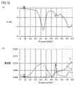
- FIG. 12 is a diagram for explaining antenna characteristics when the impedance of the antenna device 100 according to the embodiment is adjusted to the third state.
- the third state is a state in which the phase of the reflection coefficient of the first antenna ANT1 seen from the feeding circuit 30 in the first measurement state is near 0 (zero) degrees due to the phase shifter. Also, the phase difference between voltage and current is in the vicinity of 180 degrees.
- FIG. 13 is a Smith chart when the impedance of the antenna device 100 according to the embodiment is adjusted to the fourth state.
- FIG. 14 is a diagram for explaining antenna characteristics when the impedance of the antenna device 100 according to the embodiment is adjusted to the fourth state.
- the fourth state is a state in which the phase of the reflection coefficient of the first antenna ANT1 seen from the feeding circuit 30 in the first measurement state is near -90 degrees due to the phase shifter. Also, the phase difference between the voltage and the current is in the vicinity of -90 degrees.
- the antenna device 100 is provided with a phase shifter to change the impedance of the first antenna ANT1. ing.
- the antenna device 100 in the embodiment does not necessarily need to be provided with a phase shifter.
- the phase shifter need not be provided.
- Table 1 shows changes in the impedance of the first antenna ANT1 at the resonance frequency of the fundamental wave of the second antenna ANT2.
- Table 1 shows changes in the impedance of the first antenna ANT1 when the phase (difference) of the reflection coefficients is changed to 180 degrees, 90 degrees, 0 degrees, and -90 degrees.
- Re ⁇ Z ⁇ represents the real part of impedance
- Im ⁇ Z ⁇ represents the imaginary part of impedance.
- the impedance on the input side of the feeding circuit 30 is 50.0 ⁇ . The magnitude of the impedance is compared with the absolute value considering the real part and the imaginary part of the impedance.
- FIGS. 7(a), 9(a), 11(a), and 13(a) show the impedance of the first antenna ANT1, which is not coupled to the second antenna ANT2, viewed from the first radiation element 11 side. It is a figure represented as a locus
- a mark m1 indicates the impedance of the first antenna ANT1 at the resonance frequency of the fundamental wave of the second antenna ANT2.
- the mark m1 is moving clockwise.
- the impedance of the first antenna ANT1 becomes greater than 50 ⁇ . That is, when the point at the target frequency exists in the right half of the Smith chart, the impedance of the first antenna ANT1 is greater than 50 ⁇ .
- FIGS. 7(b), 9(b), 11(b), and 13(b) show the impedance of the entire antenna device 100 coupled with the second antenna ANT2 as seen from the feeding circuit 30 side on the Smith chart.
- 2 is a diagram represented as a trajectory in FIG.
- a mark m2 indicates the impedance of the entire antenna device 100 at the resonance frequency of the fundamental wave of the second antenna ANT2.
- the mark m2 is moving clockwise. Since the Smith charts shown in FIGS.
- the antenna device can The overall impedance of 100 is greater than 50 ⁇ . That is, when the point at the target frequency exists in the right half of the Smith chart, the impedance of the entire antenna device 100 is greater than 50 ⁇ .
- FIG. 4 is a diagram showing the frequency characteristics of the reflection coefficient of the device 100;
- the horizontal axis is the frequency and the vertical axis is the reflection coefficient.
- a mark m3 indicates the peak of the reflection coefficient of the antenna device 100 at the resonance frequency of the fundamental wave of the second antenna ANT2. The peak of the reflection coefficient indicated by the mark m3 decreases as the phase difference changes from 180 degrees, 90 degrees, and 0 degrees, and increases as the phase difference changes from 0 degrees to -90 degrees.
- FIGS. 8(b), 10(b), 12(b), and 14(b) show the antenna when the phase difference of the reflection coefficient is changed to 180 degrees, 90 degrees, 0 degrees, and -90 degrees.
- 4 is a diagram showing frequency characteristics of the amount of current flowing through the device 100.
- Characteristic E is the frequency characteristic of the amount of current flowing through the first antenna ANT1
- characteristic F is the frequency characteristic of the amount of current flowing through the second antenna ANT2
- characteristic G is the frequency characteristic of the amount of current flowing through the entire antenna device 100. .
- a mark m4 indicates the amount of current flowing through the second antenna ANT2 at the resonance frequency of the fundamental wave of the second antenna ANT2.
- the range surrounded by the dashed line is the range of the resonance frequency of the fundamental wave of the second antenna ANT2.
- a mark m5 indicates the amount of current flowing through the second antenna ANT2 at the third harmonic resonance frequency of the second antenna ANT2.
- the amount of current flowing through the second antenna ANT2 indicated by marks m4 and m5 decreases as the phase difference changes from 180 degrees, 90 degrees, and 0 degrees, and increases as the phase difference changes from 0 degrees to -90 degrees. In particular, when the phase difference of the reflection coefficients is 0 (zero) degrees, the amount of current flowing through the second antenna ANT2 indicated by the mark m4 is approximately 0 (zero).
- the current amount (marked m4) is smaller.
- the impedance (mark m2) of the entire antenna device 100 changes with phase differences of 180 degrees, 90 degrees, and 0 degrees as shown in FIGS. It grows larger according to That is, the antenna device 100 reduces the current flowing through the first coil L1 (primary side of the transformer) by increasing the impedance at the resonance frequency of the fundamental wave of the second antenna ANT2. The induced electromotive force generated on the secondary side) is also reduced.
- the antenna device 100 reduces the induced electromotive force generated in the second coil L2 (the secondary side of the transformer) at the resonance frequency of the fundamental wave of the second antenna ANT2, so that the resonance frequency of the fundamental wave of the second antenna ANT2 is reduced. will not resonate.
- the amount of current flowing through the second antenna ANT2 as shown in FIGS. (Mark m5) is also smaller, but the amount of current does not become substantially 0 (zero) like mark m4. Therefore, in the antenna device 100, the induced electromotive force generated in the second coil L2 (secondary side of the transformer) at the resonance frequency of the third harmonic of the second antenna ANT2 is also reduced, but the third harmonic of the second antenna ANT2 will resonate at the resonance frequency of
- the antenna device 100 adjusts the impedance of the first antenna ANT1 to be greater than 50 ⁇ at the resonance frequency of the fundamental wave of the second antenna ANT2. That is, the antenna device 100 adjusts the impedance of the first antenna ANT1 so that it is located in the right half of the Smith chart (phase difference of 90 degrees or less, 270 degrees or more). As a result, the antenna device 100 is less likely to resonate at the resonance frequency of the fundamental wave of the second antenna ANT2, and communication performance can be improved.
- the antenna device 100 includes the first antenna ANT1 and the second antenna ANT2.
- the first antenna ANT1 includes a first radiation element 11 connected to a feeding circuit 30 that supplies a high frequency signal, and a first coil L1 connected between the first radiation element 11 and the feeding circuit 30.
- the second antenna ANT2 includes a second coil L2 magnetically coupled to the first coil L1, and a second radiation element 12 connected to the second coil L2.
- the impedance of the first antenna ANT1 is greater than 50 ⁇ at the resonance frequency of the fundamental wave of the second antenna ANT2.
- the antenna device 100 can widen the frequency band to be used by adjusting the impedance of the first antenna ANT1, and obtain sufficient radiation efficiency.
- the resonance frequency of the fundamental wave of the first antenna ANT1 is preferably lower than the resonance frequency of the harmonic wave of the second antenna ANT2. Thereby, the frequency band to be used can be widened.
- the length of the second radiation element 12 is preferably longer than the length of the first radiation element 11. Thereby, the radiation efficiency of the second antenna ANT2 can be improved.
- a mobile terminal 200 (communication terminal device) includes a power supply circuit 30 and the antenna device 100 described above. This enables mobile terminal 200 to perform stable communication over a wide band.
- FIG. 15 is a circuit diagram of the antenna device 100A in Modification 1. As shown in FIG. In antenna device 100A shown in FIG. 15, the same components as those of antenna device 100 shown in FIG. 1 are denoted by the same reference numerals, and detailed description thereof will not be repeated.
- the antenna device 100A includes a first antenna ANT1 and a second antenna ANT2.
- the first antenna ANT1 includes a first radiating element 11 connected to the feeding circuit 30 and a first coil L1 connected between the first radiating element 11 and the feeding circuit.
- the second antenna ANT2 includes a second coil L2 magnetically coupled to the first coil L1, and a second radiation element 12 connected to the second coil L2.
- an impedance matching element 16 is connected between the second coil L2 and the second radiation element 12. As shown in FIG.
- the impedance matching element 16 in the second antenna ANT2 By providing the impedance matching element 16 in the second antenna ANT2, the impedance can be increased at the resonance frequency of the fundamental wave of the second antenna ANT2. By increasing the impedance with the impedance matching element 16, the amount of current flowing through the second antenna ANT2 at the resonance frequency of the fundamental wave of the second antenna ANT2 can be made smaller.
- the antenna device 100A according to Modification 1 further includes the impedance matching element 16 (second impedance matching element) connected between the second coil L2 and the second radiation element 12. Accordingly, the antenna device 100A according to Modification 1 can further reduce the amount of current flowing through the second antenna ANT2 at the resonance frequency of the fundamental wave of the second antenna ANT2.
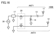
- FIG. 16 is a circuit diagram of an antenna device 100B in Modification 2. As shown in FIG. In antenna device 100B shown in FIG. 16, the same components as those of antenna device 100 shown in FIG. 1 are denoted by the same reference numerals, and detailed description thereof will not be repeated.
- the antenna device 100B includes a first antenna ANT1 and a second antenna ANT2.
- the first antenna ANT1 includes a first radiating element 11 connected to the feeding circuit 30 and a first coil L1 connected between the first radiating element 11 and the feeding circuit.
- the second antenna ANT2 includes a second coil L2 magnetically coupled to the first coil L1, and a second radiation element 12 connected to the second coil L2.
- the antenna device 100B has an impedance matching element 17 connected between the first coil L1 and the first radiation element 11 .
- the impedance matching element 17 in the first antenna ANT1 By providing the impedance matching element 17 in the first antenna ANT1, the current flowing through the first coil L1 (transformer primary side) at the resonance frequency of the fundamental wave of the second antenna ANT2 can be divided by the impedance matching element 17. By shunting the current flowing through the first coil L1 (primary side of the transformer), the amount of current flowing through the second antenna ANT2 can be made smaller at the resonance frequency of the fundamental wave of the second antenna ANT2.
- the impedance matching element 17 is a part of the first antenna ANT1, and the impedance of the first antenna ANT1 is measured with the impedance matching element 17 included.
- the antenna device 100B according to Modification 2 further includes the impedance matching element 17 (first impedance matching element) connected between the first coil L1 and the feeding circuit 30. Accordingly, the antenna device 100B according to Modification 2 can further reduce the amount of current flowing through the second antenna ANT2 at the resonance frequency of the fundamental wave of the second antenna ANT2.
- FIG. 17 is a circuit diagram of an antenna device 100C in Modification 3. As shown in FIG. In antenna device 100C shown in FIG. 17, the same components as those of antenna device 100 shown in FIG. 1 are denoted by the same reference numerals, and detailed description thereof will not be repeated.
- the antenna device 100C includes a first antenna ANT1 and a second antenna ANT2.
- the first antenna ANT1 includes a first radiating element 11 connected to the feeding circuit 30 and a first coil L1 connected between the first radiating element 11 and the feeding circuit.
- the second antenna ANT2 includes a second coil L2 magnetically coupled to the first coil L1, and a second radiation element 12 connected to the second coil L2. Furthermore, the antenna device 100C connects the capacitor 18 in parallel with the first coil L1.
- the capacitor 18 By connecting the capacitor 18 in parallel to the first coil L1, when the second antenna ANT2 is resonated at the resonance frequency of the third harmonic, the signal of the resonance frequency of the fifth harmonic or higher is sent to the transformer (first coil L1). It can be bypassed without going through the coil L1). As a result, it is possible to prevent the second antenna ANT2 from resonating at unnecessary resonance frequencies equal to or higher than the fifth harmonic.
- the antenna device 100C according to Modification 3 further includes the capacitor 18 that is connected in parallel with the first coil L1.
- the antenna device 100C according to Modification 3 can prevent the second antenna ANT2 from resonating at unnecessary resonance frequencies equal to or higher than the fifth harmonic.
- FIG. 18 is a circuit diagram of an antenna device 100D in Modification 4. As shown in FIG. In antenna device 100D shown in FIG. 18, the same components as those of antenna device 100 shown in FIG. 1 are denoted by the same reference numerals, and detailed description thereof will not be repeated.
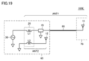
- the first radiating element 11 and the second radiating element 12 are not formed on the same substrate, and the first radiating element 11 is formed on a sub substrate 70 different from the main substrate 60 on which the second radiating element 12 is provided. 11 are formed.
- the main substrate 60 includes a power supply circuit 30 connected to the first radiation element 11, a first coil L1 connected between the first radiation element 11 and the power supply circuit, and a magnetically coupled circuit for the first coil L1. and a second radiation element 12 connected to the second coil L2.
- the first coil L1 and the second coil L2 constitute an antenna coupling element 20. As shown in FIG.
- the first radiation element 11 formed on the sub-board 70 and the first coil L1 formed on the main board 60 are connected by a coaxial cable 80 .
- the degree of freedom in arranging the first radiating element 11 is increased.
- the second radiation element 12, which is a parasitic element is formed on the main substrate 60, the second radiation element 12 can radiate radio waves from the second coil L2 without passing through a long transmission line. can be done. Therefore, transmission loss can be reduced in the second radiation element 12 .
- the transmission line that connects the main board 60 and the sub-board 70 is not limited to the coaxial cable 80, and may be a printed circuit board (PCB), a flexible printed circuit board (FPC), or a MetroCirc (registered trademark). and so on.
- Metrocirc (registered trademark) is a resin multilayer substrate in which multiple sheets of liquid crystal polymer (LCP) are laminated.
- the first radiation element 11 and the first coil L1 are connected by the coaxial cable 80, and the first radiation element 11 can be formed on the sub-board 70.
- the main substrate 60 and the sub-substrate 70 are examples, and the substrates forming the first radiation element 11 and the substrates forming the second radiation element 12 may be different substrates.
- FIG. 19 is a circuit diagram of an antenna device 100E in Modification 5. As shown in FIG. In antenna device 100E shown in FIG. 19, the same components as those of antenna device 100 shown in FIG. 1 and antenna device 100D shown in FIG. 18 are denoted by the same reference numerals, and detailed description thereof will not be repeated.
- the impedance matching element 19 is connected between the first coil L1 and the connection point of the coaxial cable 80.
- the impedance matching element 19 third impedance matching element
- the first antenna ANT1 is resonated at the resonance frequency of the fundamental wave
- the second antenna ANT2 is resonated at the triple harmonic resonance frequency.
- the present invention is not limited to this, and the antenna device 100 may resonate the first antenna ANT1 at the third harmonic resonance frequency and the second antenna ANT2 at the third harmonic resonance frequency.
- the first antenna ANT1 may also be caused to resonate at the resonance frequency of the fundamental wave.
- the antenna device 100 can also use the frequency band including the resonance frequency of the fundamental wave of the first antenna ANT1.
- the antenna device 100 may resonate the second antenna ANT2 at a resonance frequency other than the third harmonic.
- the length of the radiating element increases as the resonance frequency decreases. Therefore, if the second antenna ANT2 is resonated at the resonance frequency of the harmonic higher than three times, the resonance frequency of the fundamental wave becomes lower, so the length of the second radiating element 12 can be made longer. .
- the antenna device 100 is configured to excite the second antenna ANT2 in a higher frequency band including n79 with respect to the first antenna ANT1 that is excited in the band including n78.
- the antenna device 100 may be configured to excite the second antenna ANT2 in a lower frequency band than the first antenna ANT1 that excites in the band including n78.
- the antenna coupling element 20 may be additive or depolar.
Landscapes
- Engineering & Computer Science (AREA)
- Computer Networks & Wireless Communication (AREA)
- Details Of Aerials (AREA)
- Physics & Mathematics (AREA)
- Electromagnetism (AREA)
Priority Applications (3)
| Application Number | Priority Date | Filing Date | Title |
|---|---|---|---|
| JP2023545151A JP7568122B2 (ja) | 2021-09-03 | 2022-07-21 | アンテナ装置、および通信端末装置 |
| CN202280059631.3A CN117916953A (zh) | 2021-09-03 | 2022-07-21 | 天线装置以及通信终端装置 |
| US18/418,455 US12407090B2 (en) | 2021-09-03 | 2024-01-22 | Antenna device and communication terminal device |
Applications Claiming Priority (4)
| Application Number | Priority Date | Filing Date | Title |
|---|---|---|---|
| JP2021144106 | 2021-09-03 | ||
| JP2021-144106 | 2021-09-03 | ||
| JP2021173126 | 2021-10-22 | ||
| JP2021-173126 | 2021-10-22 |
Related Child Applications (1)
| Application Number | Title | Priority Date | Filing Date |
|---|---|---|---|
| US18/418,455 Continuation US12407090B2 (en) | 2021-09-03 | 2024-01-22 | Antenna device and communication terminal device |
Publications (1)
| Publication Number | Publication Date |
|---|---|
| WO2023032511A1 true WO2023032511A1 (ja) | 2023-03-09 |
Family
ID=85412131
Family Applications (1)
| Application Number | Title | Priority Date | Filing Date |
|---|---|---|---|
| PCT/JP2022/028381 Ceased WO2023032511A1 (ja) | 2021-09-03 | 2022-07-21 | アンテナ装置、および通信端末装置 |
Country Status (3)
| Country | Link |
|---|---|
| US (1) | US12407090B2 (https=) |
| JP (1) | JP7568122B2 (https=) |
| WO (1) | WO2023032511A1 (https=) |
Cited By (1)
| Publication number | Priority date | Publication date | Assignee | Title |
|---|---|---|---|---|
| WO2025134482A1 (ja) * | 2023-12-20 | 2025-06-26 | 株式会社村田製作所 | アンテナ装置、および通信端末装置 |
Citations (4)
| Publication number | Priority date | Publication date | Assignee | Title |
|---|---|---|---|---|
| WO2012153654A1 (ja) * | 2011-05-09 | 2012-11-15 | 株式会社村田製作所 | フロントエンド回路および通信端末装置 |
| JP2014053808A (ja) * | 2012-09-07 | 2014-03-20 | Murata Mfg Co Ltd | 結合度調整素子、アンテナ装置および無線通信装置 |
| WO2018101284A1 (ja) * | 2016-11-29 | 2018-06-07 | 株式会社村田製作所 | アンテナ装置および電子機器 |
| WO2020219160A1 (en) * | 2019-04-26 | 2020-10-29 | Palstar, Inc. | Automatic impedance matching system, method and apparatus |
Family Cites Families (1)
| Publication number | Priority date | Publication date | Assignee | Title |
|---|---|---|---|---|
| JP6760545B2 (ja) | 2018-04-25 | 2020-09-23 | 株式会社村田製作所 | アンテナ結合素子、アンテナ装置及び通信端末装置 |
-
2022
- 2022-07-21 JP JP2023545151A patent/JP7568122B2/ja active Active
- 2022-07-21 WO PCT/JP2022/028381 patent/WO2023032511A1/ja not_active Ceased
-
2024
- 2024-01-22 US US18/418,455 patent/US12407090B2/en active Active
Patent Citations (4)
| Publication number | Priority date | Publication date | Assignee | Title |
|---|---|---|---|---|
| WO2012153654A1 (ja) * | 2011-05-09 | 2012-11-15 | 株式会社村田製作所 | フロントエンド回路および通信端末装置 |
| JP2014053808A (ja) * | 2012-09-07 | 2014-03-20 | Murata Mfg Co Ltd | 結合度調整素子、アンテナ装置および無線通信装置 |
| WO2018101284A1 (ja) * | 2016-11-29 | 2018-06-07 | 株式会社村田製作所 | アンテナ装置および電子機器 |
| WO2020219160A1 (en) * | 2019-04-26 | 2020-10-29 | Palstar, Inc. | Automatic impedance matching system, method and apparatus |
Cited By (1)
| Publication number | Priority date | Publication date | Assignee | Title |
|---|---|---|---|---|
| WO2025134482A1 (ja) * | 2023-12-20 | 2025-06-26 | 株式会社村田製作所 | アンテナ装置、および通信端末装置 |
Also Published As
| Publication number | Publication date |
|---|---|
| US20240162611A1 (en) | 2024-05-16 |
| US12407090B2 (en) | 2025-09-02 |
| JP7568122B2 (ja) | 2024-10-16 |
| JPWO2023032511A1 (https=) | 2023-03-09 |
Similar Documents
| Publication | Publication Date | Title |
|---|---|---|
| JP6614363B2 (ja) | アンテナ装置および電子機器 | |
| TWI466375B (zh) | An antenna device and a communication terminal device | |
| US9019168B2 (en) | Frequency stabilization circuit, frequency stabilization device, antenna apparatus and communication terminal equipment, and impedance conversion element | |
| JP6465109B2 (ja) | マルチアンテナ及びそれを備える無線装置 | |
| JP5526131B2 (ja) | アンテナ装置及び無線通信装置 | |
| CN103141031B (zh) | 阻抗变换电路以及通信终端装置 | |
| CN207075005U (zh) | 天线匹配电路、天线装置以及通信终端装置 | |
| US11764473B2 (en) | Apparatus with partitioned radio frequency antenna and matching network and associated methods | |
| JP6753554B2 (ja) | アンテナ装置及び通信端末装置 | |
| WO2014203977A1 (ja) | アンテナ、アンテナ装置及び無線装置 | |
| WO2014034587A1 (ja) | アンテナ装置および通信端末装置 | |
| CN212676477U (zh) | 天线装置以及通信终端装置 | |
| JP2007013958A (ja) | アンテナシステム | |
| US20150009093A1 (en) | Antenna apparatus and portable wireless device equipped with the same | |
| JPWO2019208297A1 (ja) | アンテナ結合素子、アンテナ装置及び通信端末装置 | |
| WO2012029793A1 (ja) | アンテナ | |
| JP7568122B2 (ja) | アンテナ装置、および通信端末装置 | |
| US20250239780A1 (en) | Antenna device and electronic apparatus | |
| CN101459284B (zh) | 天线装置 | |
| JP6233319B2 (ja) | マルチバンドアンテナ及び無線装置 | |
| JPWO2005004276A1 (ja) | 携帯無線機 | |
| CN117916953A (zh) | 天线装置以及通信终端装置 | |
| US11894623B2 (en) | Apparatus with partitioned radio frequency antenna and matching network and associated methods | |
| JP2005110144A (ja) | マッチング回路及びアンテナ装置 | |
| KR20110003679A (ko) | 접지면 패치를 이용한 모노폴 칩 안테나 |
Legal Events
| Date | Code | Title | Description |
|---|---|---|---|
| 121 | Ep: the epo has been informed by wipo that ep was designated in this application |
Ref document number: 22864099 Country of ref document: EP Kind code of ref document: A1 |
|
| WWE | Wipo information: entry into national phase |
Ref document number: 2023545151 Country of ref document: JP |
|
| WWE | Wipo information: entry into national phase |
Ref document number: 202280059631.3 Country of ref document: CN |
|
| NENP | Non-entry into the national phase |
Ref country code: DE |
|
| 122 | Ep: pct application non-entry in european phase |
Ref document number: 22864099 Country of ref document: EP Kind code of ref document: A1 |