WO2023032511A1 - Antenna device and communication terminal device - Google Patents
Antenna device and communication terminal device Download PDFInfo
- Publication number
- WO2023032511A1 WO2023032511A1 PCT/JP2022/028381 JP2022028381W WO2023032511A1 WO 2023032511 A1 WO2023032511 A1 WO 2023032511A1 JP 2022028381 W JP2022028381 W JP 2022028381W WO 2023032511 A1 WO2023032511 A1 WO 2023032511A1
- Authority
- WO
- WIPO (PCT)
- Prior art keywords
- antenna
- coil
- antenna device
- impedance
- ant2
- Prior art date
Links
- 238000004891 communication Methods 0.000 title claims abstract description 16
- 230000005855 radiation Effects 0.000 claims abstract description 70
- 239000000758 substrate Substances 0.000 claims description 20
- 239000003990 capacitor Substances 0.000 claims description 8
- 102100026396 ADP/ATP translocase 2 Human genes 0.000 description 89
- 101000718417 Homo sapiens ADP/ATP translocase 2 Proteins 0.000 description 89
- 102100032533 ADP/ATP translocase 1 Human genes 0.000 description 57
- 101000768061 Escherichia phage P1 Antirepressor protein 1 Proteins 0.000 description 57
- 101000796932 Homo sapiens ADP/ATP translocase 1 Proteins 0.000 description 57
- 238000010586 diagram Methods 0.000 description 28
- 238000012986 modification Methods 0.000 description 24
- 230000004048 modification Effects 0.000 description 24
- 230000008878 coupling Effects 0.000 description 19
- 238000010168 coupling process Methods 0.000 description 19
- 238000005859 coupling reaction Methods 0.000 description 19
- 238000005259 measurement Methods 0.000 description 19
- 229920000106 Liquid crystal polymer Polymers 0.000 description 5
- 239000004977 Liquid-crystal polymers (LCPs) Substances 0.000 description 5
- 230000005540 biological transmission Effects 0.000 description 5
- 239000000463 material Substances 0.000 description 5
- 230000003071 parasitic effect Effects 0.000 description 5
- 239000000919 ceramic Substances 0.000 description 4
- 239000004020 conductor Substances 0.000 description 4
- 230000007423 decrease Effects 0.000 description 4
- RYGMFSIKBFXOCR-UHFFFAOYSA-N Copper Chemical compound [Cu] RYGMFSIKBFXOCR-UHFFFAOYSA-N 0.000 description 2
- 238000010030 laminating Methods 0.000 description 2
- 238000010295 mobile communication Methods 0.000 description 2
- 230000010363 phase shift Effects 0.000 description 2
- 239000011347 resin Substances 0.000 description 2
- 229920005989 resin Polymers 0.000 description 2
- 239000000654 additive Substances 0.000 description 1
- 230000000996 additive effect Effects 0.000 description 1
- 239000010949 copper Substances 0.000 description 1
- 229910052802 copper Inorganic materials 0.000 description 1
- 239000011889 copper foil Substances 0.000 description 1
- 238000005516 engineering process Methods 0.000 description 1
- 239000011521 glass Substances 0.000 description 1
- 230000002452 interceptive effect Effects 0.000 description 1
- 230000007774 longterm Effects 0.000 description 1
- 230000005404 monopole Effects 0.000 description 1
- 238000007650 screen-printing Methods 0.000 description 1
- 229910000859 α-Fe Inorganic materials 0.000 description 1
Images


Classifications
-
- H—ELECTRICITY
- H01—ELECTRIC ELEMENTS
- H01Q—ANTENNAS, i.e. RADIO AERIALS
- H01Q1/00—Details of, or arrangements associated with, antennas
- H01Q1/50—Structural association of antennas with earthing switches, lead-in devices or lightning protectors
-
- H—ELECTRICITY
- H03—ELECTRONIC CIRCUITRY
- H03H—IMPEDANCE NETWORKS, e.g. RESONANT CIRCUITS; RESONATORS
- H03H7/00—Multiple-port networks comprising only passive electrical elements as network components
- H03H7/38—Impedance-matching networks
Definitions
- the present disclosure relates to technology of antenna devices and communication terminal devices.
- Patent Document 1 discloses an antenna device in which two antennas, a fed antenna and a parasitic antenna, are coupled.
- the resonance frequency is not so high, so the length of the antenna is sufficient (the length of the radiating element) can be ensured.
- the length of the antenna becomes shorter as the resonance frequency becomes higher. Therefore, for example, when used in the frequency band (3.3 to 5.0 GHz) used in the 5th generation mobile communication system (5G), the antenna device has a short parasitic antenna length and sufficient radiation efficiency. could not be obtained.
- the present disclosure has been made to solve such problems, and its object is to provide an antenna device and a communication terminal device that can obtain sufficient radiation efficiency while widening the frequency band to be used. be.
- An antenna device is an antenna device comprising a first antenna and a second antenna.
- the first antenna includes a first radiating element connected to a feeding circuit that supplies a high frequency signal, and a first coil connected between the first antenna and the feeding circuit.
- the second antenna includes a second coil magnetically coupled to the first coil and a second radiating element connected to the second coil.
- the impedance of the first antenna is greater than 50 ⁇ at the resonant frequency of the fundamental wave of the second antenna.
- a communication terminal device includes a feeding circuit and the antenna device described above.
- the impedance of the first antenna is greater than 50 ⁇ at the resonance frequency of the fundamental wave of the second antenna, the frequency band to be used can be widened and sufficient radiation efficiency can be obtained. be done.
- FIG. 1 is a circuit diagram of an antenna device according to an embodiment;
- FIG. 1 is a schematic diagram showing a communication terminal device in an embodiment;
- FIG. It is a schematic diagram showing a configuration for measuring the impedance of the first antenna in the embodiment.
- It is a schematic diagram showing a configuration for measuring the impedance of the second antenna in the embodiment.
- It is a figure which shows the frequency characteristic of the reflection coefficient of the antenna device in embodiment.
- It is a figure which shows the Smith chart at the time of adjusting the impedance of the antenna device in embodiment to a 1st state.
- FIG. 10 is a circuit diagram of an antenna device according to Modification 1;
- FIG. 11 is a circuit diagram of an antenna device in Modification 2;
- FIG. 11 is a circuit diagram of an antenna device in Modification 3;
- FIG. 11 is a circuit diagram of an antenna device in Modification 4;
- FIG. 11 is a circuit diagram of an antenna device in Modification 5;
- FIG. 1 is a circuit diagram of an antenna device 100 according to an embodiment.
- the antenna device 100 includes a first antenna ANT1 and a second antenna ANT2.
- the first antenna ANT1 includes a first radiating element 11 connected to the feeding circuit 30 and a first coil L1 connected between the first radiating element 11 and the feeding circuit.
- the second antenna ANT2 includes a second coil L2 magnetically coupled to the first coil L1, and a second radiation element 12 connected to the second coil L2. Therefore, the first antenna ANT1 is a fed antenna that is fed by the feeding circuit 30, and the second antenna ANT2 is not connected to the feeding circuit 30 and is a parasitic antenna that is not fed by the feeding circuit 30.
- a first antenna ANT1 to which power is supplied is provided with a capacitor 13 connected in series and a coil 14 to which one end is connected. The other end of the coil 14 is connected to GND.
- a capacitor 13 and a coil 14 form an LC circuit and function as a filter circuit for the first antenna ANT1. Note that if the filter circuit is unnecessary in the first antenna ANT1, the capacitor 13 and the coil 14 need not be provided.
- the first antenna ANT1 and the second antenna ANT2 are magnetically coupled by the first coil L1 and the second coil L2 in order to widen the usable frequency band. That is, the first coil L1 and the second coil L2 constitute the antenna coupling element 20. As shown in FIG.
- the antenna coupling element 20 is a rectangular parallelepiped chip part mounted on a circuit board in an electronic device.
- the antenna coupling element 20 uses a liquid crystal polymer (LCP [Liquid Crystal Polymer]) sheet as the insulating base material, and copper foil is used to form the first coil L1 and the second coil L1. It is constructed by laminating each insulating base material on which the conductor pattern of the coil L2 is patterned.
- LCP Liquid Crystal Polymer
- the antenna coupling element 20 when the antenna coupling element 20 is composed of a ceramic multilayer substrate, the antenna coupling element 20 uses low temperature co-fired ceramics (LTCC [Low Temperature Co-fired Ceramics]) for the insulating base material, and copper paste is printed. It is configured by laminating respective insulating base materials formed and patterned with conductor patterns of the first coil L1 and the second coil L2. Furthermore, the antenna coupling element 20 is not limited to the ceramic multilayer substrate, and may be formed by, for example, repeatedly applying an insulating paste containing glass as a main component by screen printing. As described above, the antenna coupling element 20 can be used as a transformer with a predetermined inductance and a predetermined coupling coefficient because the insulating base material is non-magnetic (not magnetic ferrite).
- LTCC Low Temperature Co-fired Ceramics
- the antenna device 100 can cover a wide band by connecting two radiation elements (the first radiation element 11 and the second radiation element 12) to the antenna coupling element 20.
- the antenna device 100 covers the frequency band (3.3 to 5.0 GHz) used in the fifth generation mobile communication system (5G) or the frequency band such as the 5 GHz band wireless LAN
- the second antenna ANT2 is required to resonate at a high resonance frequency, and the length of the second radiating element 12 is shortened.
- the length of the second radiation element 12 is shortened, sufficient radiation efficiency may not be obtained.
- the length of the second radiation element 12 can be lengthened by resonating the second antenna ANT2 not at the resonant frequency of the fundamental wave but at the resonant frequency of the harmonic wave. That is, when the resonance frequency to be resonated in the second antenna ANT2 is, for example, 4.4 GHz, the length of the second radiation element 12 is shortened when the second antenna ANT2 is resonated with the fundamental wave of 4.4 GHz. However, when resonating the second antenna ANT2 with the triple harmonic of 4.4 GHz, the resonance frequency of the fundamental wave is 1.4 GHz.
- the length of the radiating element 12 By defining the length of the second radiating element 12 with the resonant frequency of the fundamental wave of 1.4 GHz, the length of the radiating element can be made longer than when the length of the second radiating element 12 is defined with the resonant frequency of the fundamental wave of 4.4 GHz. can.
- the length of the second radiation element 12 is lengthened by causing the second antenna ANT2 to resonate at the resonant frequency of the harmonic, and sufficient radiation efficiency can be obtained.
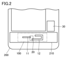
- FIG. 2 is a schematic diagram showing a communication terminal device according to the embodiment.
- the communication terminal device shown in FIG. 2 is a mobile terminal 200 capable of communication in a band including n78 (3.3-3.8 GHz) and a band including n79 (4.4-4.9 GHz). Therefore, mobile terminal 200 is provided with antenna device 100 including first antenna ANT1 excited in a band including n78 and second antenna ANT2 excited in a band including n79.
- the mobile terminal 200 is, for example, a mobile phone, a smart phone, a tablet, or the like.
- the antenna device 100 has an antenna coupling element 20 provided on the back side of a substrate 210 on which the first radiation element 11 and the second radiation element 12 are patterned, and couples the first antenna ANT1 and the second antenna ANT2. Also, although the first antenna ANT1 is electrically connected to the feeding circuit 30 by wiring (not shown), the second antenna ANT2 is not electrically connected to the feeding circuit 30. FIG.
- the first radiation element 11 is composed of a linear conductor pattern extending from the antenna coupling element 20 in the left direction in the drawing.
- the second radiating element 12 is composed of a linear conductor pattern that extends from the antenna coupling element 20 in the right direction in the drawing and turns back in the left direction in the middle. Both the first radiating element 11 and the second radiating element 12 act as a monopole antenna.
- the first antenna ANT1 is excited in a band including n78, and the second antenna ANT2 is excited in a band including n79.
- First radiating element 11 is longer than 12 .
- the second antenna ANT2 resonates at the third harmonic resonance frequency, the length of the radiation element is longer in the second radiation element 12 than in the first radiation element 11, as shown in FIG. there is
- the second antenna ANT2 is resonated at the fundamental resonance frequency.
- the resonance frequency of the fundamental wave of the second antenna ANT2 is not included in the frequency band targeted by the antenna device 100, and the second antenna ANT2 resonates at the resonance frequency of the fundamental wave, the antenna device 100 Interfering waves outside the frequency band are received, and communication performance deteriorates.
- the antenna device 100 adjusts the impedance so as not to resonate at the resonance frequency of the fundamental wave of the second antenna ANT2. Specifically, the antenna device 100 adjusts the impedance of the first antenna ANT1 to be, for example, greater than 50 ⁇ at the resonance frequency of the fundamental wave of the second antenna ANT2.
- the figure of 50 ⁇ is a reference value that is also used in general antenna design, and if the impedance is higher than this, the current flowing through the circuit will decrease. Further, in a general antenna design, the impedance on the input side of the feeding circuit 30 also corresponds to around 50 ⁇ .
- the case where "the target impedance is greater than 50 ⁇ " corresponds to the case where "the target impedance is greater than the impedance on the input side of the feeding circuit 30". Also, in this specification, the magnitude of impedance is compared with an absolute value that takes into consideration the real part and the imaginary part of impedance.
- FIG. 3 is a schematic diagram showing the configuration for measuring the impedance of the first antenna ANT1 according to the embodiment.
- the impedance of the first antenna ANT1 is measured by connecting the network analyzer 50 with the measurement cable 51 to the first coil L1 instead of the feeding circuit 30 as shown in FIG.
- the second radiation element 12 and GND are removed from the second coil L2 to open both ends of the second coil L2.
- the frequency characteristic of the impedance of the first antenna ANT1 is measured by the network analyzer 50 with the connection point between the first coil L1 and the measurement cable 51 as the measurement point t1.
- the phase shift due to the length of the measurement cable 51 is calibrated in advance at the connection point with the first coil L1 on the primary side of the transformer.
- FIG. 4 is a schematic diagram showing a configuration for measuring the impedance of the second antenna ANT2 in the embodiment. Measurement of the resonance frequency of the fundamental wave of the second antenna ANT2 is performed in the second measurement state by connecting the network analyzer 50 to the second coil L2 with the measurement cable 52 instead of connecting to GND as shown in FIG. . At this time, if the first coil L1 and the second coil L2 are integrally formed as an element and it is difficult to separate them, the first radiation element 11 and the feeding circuit 30 are removed from the first coil L1, and both ends of the first coil L1 are opened.
- the frequency characteristic of the fundamental wave of the second antenna ANT2 is measured by the network analyzer 50 with the connection point between the second coil L2 and the measurement cable 52 as the measurement point t2. This measurement allows the resonance frequency of the parasitic element to be identified.
- the phase shift due to the length of the measurement cable 52 is calibrated in advance at the connection point with the second coil L2 on the secondary side of the transformer.
- the impedance of the first antenna ANT1 at the resonance frequency of the fundamental wave of the second antenna ANT2 can be specified by the measurements in the first and second measurement states.
- the antenna device 100 can achieve the first coil L1 (primary side) is reduced. Therefore, the induced electromotive force generated in the second coil L2 (secondary side of the transformer) is also reduced, and even if the second antenna ANT2 itself resonates at the resonance frequency of the fundamental wave, the antenna device 100 as a whole can will not resonate at the resonance frequency of the fundamental wave of
- FIG. 5 is a diagram showing the frequency characteristics of the reflection coefficient of the antenna device 100 according to the embodiment.
- the horizontal axis is frequency and the vertical axis is reflection coefficient.
- the reflection coefficient A is the reflection coefficient when the antenna coupling element 20 side is viewed from the feeding circuit 30 in FIG. 1 (that is, the reflection coefficient of the antenna device 100).
- a reflection coefficient B is a reflection coefficient of the first radiation element 11 side viewed from the first coil L1 in FIG. 1 (that is, of the first antenna ANT1).
- resonance occurs at the resonance frequency of the fundamental wave of the first antenna ANT1 (the resonance frequency of the first coil L1 and the first radiation element 11) in the band including n78, and the second antenna ANT2 occurs in the band including n79.
- Resonance occurs at the resonance frequency (eg, 4.8 GHz) of the third harmonic due to .
- resonance coefficient B resonance occurs at the resonance frequency of the fundamental wave of the first antenna ANT1 in the band including n78. That is, in the antenna device 100, by coupling the second antenna ANT2 to the first antenna ANT1 with the antenna coupling element 20, it is possible to widen the band up to the band including n79.
- the antenna device 100 By adjusting the impedance of the antenna device 100 as described above, no resonance is observed at the resonance frequency (for example, 1.5 GHz) of the fundamental wave of the second antenna ANT2 at the reflection coefficient A. That is, the antenna device 100 does not operate at the resonance frequency of the fundamental wave of the second antenna ANT2.
- FIG. 6 is a diagram for explaining the radiation efficiency of the antenna device 100 according to the embodiment.
- the horizontal axis is frequency and the vertical axis is radiation efficiency.
- the characteristic C is the frequency characteristic of the radiation efficiency of the antenna device 100 when the second antenna ANT2 is resonated at the resonance frequency of the third harmonic
- the characteristic D is the frequency characteristic of the second antenna ANT2 at the resonance frequency of the fundamental wave. 4 shows the frequency characteristics of the radiation efficiency of the antenna device when resonating at . Since the length of the second radiation element 12 can be increased when the second antenna ANT2 is resonated at the resonance frequency of the third harmonic, the antenna device 100 can reduce n79 as indicated by the characteristic C. The radiation efficiency is improved in the band including.
- FIG. 7 is a Smith chart when the impedance of the antenna device 100 according to the embodiment is adjusted to the first state.
- FIG. 8 is a diagram for explaining antenna characteristics when the impedance of the antenna device 100 according to the embodiment is adjusted to the first state.
- the first state is a state in which the phase of the reflection coefficient of the first antenna ANT1 seen from the feeding circuit 30 in the first measurement state is around 180 degrees due to the phase shifter.
- the phase of the reflection coefficient is the angle formed by the line connecting the point of the target frequency and the center in the counterclockwise direction starting from the X-axis on the right side of the center of the Smith chart.
- FIG. 9 is a diagram showing a Smith chart when the impedance of the antenna device 100 according to the embodiment is adjusted to the second state.
- FIG. 10 is a diagram for explaining antenna characteristics when the impedance of the antenna device 100 according to the embodiment is adjusted to the second state.
- the second state is a state in which the phase of the reflection coefficient of the first antenna ANT1 seen from the feeding circuit 30 in the first measurement state is near 90 degrees due to the phase shifter. Also, the phase difference between the voltage and the current is in the vicinity of 90 degrees.
- FIG. 11 is a Smith chart when the impedance of the antenna device 100 according to the embodiment is adjusted to the third state.
- FIG. 12 is a diagram for explaining antenna characteristics when the impedance of the antenna device 100 according to the embodiment is adjusted to the third state.
- the third state is a state in which the phase of the reflection coefficient of the first antenna ANT1 seen from the feeding circuit 30 in the first measurement state is near 0 (zero) degrees due to the phase shifter. Also, the phase difference between voltage and current is in the vicinity of 180 degrees.
- FIG. 13 is a Smith chart when the impedance of the antenna device 100 according to the embodiment is adjusted to the fourth state.
- FIG. 14 is a diagram for explaining antenna characteristics when the impedance of the antenna device 100 according to the embodiment is adjusted to the fourth state.
- the fourth state is a state in which the phase of the reflection coefficient of the first antenna ANT1 seen from the feeding circuit 30 in the first measurement state is near -90 degrees due to the phase shifter. Also, the phase difference between the voltage and the current is in the vicinity of -90 degrees.
- the antenna device 100 is provided with a phase shifter to change the impedance of the first antenna ANT1. ing.
- the antenna device 100 in the embodiment does not necessarily need to be provided with a phase shifter.
- the phase shifter need not be provided.
- Table 1 shows changes in the impedance of the first antenna ANT1 at the resonance frequency of the fundamental wave of the second antenna ANT2.
- Table 1 shows changes in the impedance of the first antenna ANT1 when the phase (difference) of the reflection coefficients is changed to 180 degrees, 90 degrees, 0 degrees, and -90 degrees.
- Re ⁇ Z ⁇ represents the real part of impedance
- Im ⁇ Z ⁇ represents the imaginary part of impedance.
- the impedance on the input side of the feeding circuit 30 is 50.0 ⁇ . The magnitude of the impedance is compared with the absolute value considering the real part and the imaginary part of the impedance.
- FIGS. 7(a), 9(a), 11(a), and 13(a) show the impedance of the first antenna ANT1, which is not coupled to the second antenna ANT2, viewed from the first radiation element 11 side. It is a figure represented as a locus
- a mark m1 indicates the impedance of the first antenna ANT1 at the resonance frequency of the fundamental wave of the second antenna ANT2.
- the mark m1 is moving clockwise.
- the impedance of the first antenna ANT1 becomes greater than 50 ⁇ . That is, when the point at the target frequency exists in the right half of the Smith chart, the impedance of the first antenna ANT1 is greater than 50 ⁇ .
- FIGS. 7(b), 9(b), 11(b), and 13(b) show the impedance of the entire antenna device 100 coupled with the second antenna ANT2 as seen from the feeding circuit 30 side on the Smith chart.
- 2 is a diagram represented as a trajectory in FIG.
- a mark m2 indicates the impedance of the entire antenna device 100 at the resonance frequency of the fundamental wave of the second antenna ANT2.
- the mark m2 is moving clockwise. Since the Smith charts shown in FIGS.
- the antenna device can The overall impedance of 100 is greater than 50 ⁇ . That is, when the point at the target frequency exists in the right half of the Smith chart, the impedance of the entire antenna device 100 is greater than 50 ⁇ .
- FIG. 4 is a diagram showing the frequency characteristics of the reflection coefficient of the device 100;
- the horizontal axis is the frequency and the vertical axis is the reflection coefficient.
- a mark m3 indicates the peak of the reflection coefficient of the antenna device 100 at the resonance frequency of the fundamental wave of the second antenna ANT2. The peak of the reflection coefficient indicated by the mark m3 decreases as the phase difference changes from 180 degrees, 90 degrees, and 0 degrees, and increases as the phase difference changes from 0 degrees to -90 degrees.
- FIGS. 8(b), 10(b), 12(b), and 14(b) show the antenna when the phase difference of the reflection coefficient is changed to 180 degrees, 90 degrees, 0 degrees, and -90 degrees.
- 4 is a diagram showing frequency characteristics of the amount of current flowing through the device 100.
- Characteristic E is the frequency characteristic of the amount of current flowing through the first antenna ANT1
- characteristic F is the frequency characteristic of the amount of current flowing through the second antenna ANT2
- characteristic G is the frequency characteristic of the amount of current flowing through the entire antenna device 100. .
- a mark m4 indicates the amount of current flowing through the second antenna ANT2 at the resonance frequency of the fundamental wave of the second antenna ANT2.
- the range surrounded by the dashed line is the range of the resonance frequency of the fundamental wave of the second antenna ANT2.
- a mark m5 indicates the amount of current flowing through the second antenna ANT2 at the third harmonic resonance frequency of the second antenna ANT2.
- the amount of current flowing through the second antenna ANT2 indicated by marks m4 and m5 decreases as the phase difference changes from 180 degrees, 90 degrees, and 0 degrees, and increases as the phase difference changes from 0 degrees to -90 degrees. In particular, when the phase difference of the reflection coefficients is 0 (zero) degrees, the amount of current flowing through the second antenna ANT2 indicated by the mark m4 is approximately 0 (zero).
- the current amount (marked m4) is smaller.
- the impedance (mark m2) of the entire antenna device 100 changes with phase differences of 180 degrees, 90 degrees, and 0 degrees as shown in FIGS. It grows larger according to That is, the antenna device 100 reduces the current flowing through the first coil L1 (primary side of the transformer) by increasing the impedance at the resonance frequency of the fundamental wave of the second antenna ANT2. The induced electromotive force generated on the secondary side) is also reduced.
- the antenna device 100 reduces the induced electromotive force generated in the second coil L2 (the secondary side of the transformer) at the resonance frequency of the fundamental wave of the second antenna ANT2, so that the resonance frequency of the fundamental wave of the second antenna ANT2 is reduced. will not resonate.
- the amount of current flowing through the second antenna ANT2 as shown in FIGS. (Mark m5) is also smaller, but the amount of current does not become substantially 0 (zero) like mark m4. Therefore, in the antenna device 100, the induced electromotive force generated in the second coil L2 (secondary side of the transformer) at the resonance frequency of the third harmonic of the second antenna ANT2 is also reduced, but the third harmonic of the second antenna ANT2 will resonate at the resonance frequency of
- the antenna device 100 adjusts the impedance of the first antenna ANT1 to be greater than 50 ⁇ at the resonance frequency of the fundamental wave of the second antenna ANT2. That is, the antenna device 100 adjusts the impedance of the first antenna ANT1 so that it is located in the right half of the Smith chart (phase difference of 90 degrees or less, 270 degrees or more). As a result, the antenna device 100 is less likely to resonate at the resonance frequency of the fundamental wave of the second antenna ANT2, and communication performance can be improved.
- the antenna device 100 includes the first antenna ANT1 and the second antenna ANT2.
- the first antenna ANT1 includes a first radiation element 11 connected to a feeding circuit 30 that supplies a high frequency signal, and a first coil L1 connected between the first radiation element 11 and the feeding circuit 30.
- the second antenna ANT2 includes a second coil L2 magnetically coupled to the first coil L1, and a second radiation element 12 connected to the second coil L2.
- the impedance of the first antenna ANT1 is greater than 50 ⁇ at the resonance frequency of the fundamental wave of the second antenna ANT2.
- the antenna device 100 can widen the frequency band to be used by adjusting the impedance of the first antenna ANT1, and obtain sufficient radiation efficiency.
- the resonance frequency of the fundamental wave of the first antenna ANT1 is preferably lower than the resonance frequency of the harmonic wave of the second antenna ANT2. Thereby, the frequency band to be used can be widened.
- the length of the second radiation element 12 is preferably longer than the length of the first radiation element 11. Thereby, the radiation efficiency of the second antenna ANT2 can be improved.
- a mobile terminal 200 (communication terminal device) includes a power supply circuit 30 and the antenna device 100 described above. This enables mobile terminal 200 to perform stable communication over a wide band.
- FIG. 15 is a circuit diagram of the antenna device 100A in Modification 1. As shown in FIG. In antenna device 100A shown in FIG. 15, the same components as those of antenna device 100 shown in FIG. 1 are denoted by the same reference numerals, and detailed description thereof will not be repeated.
- the antenna device 100A includes a first antenna ANT1 and a second antenna ANT2.
- the first antenna ANT1 includes a first radiating element 11 connected to the feeding circuit 30 and a first coil L1 connected between the first radiating element 11 and the feeding circuit.
- the second antenna ANT2 includes a second coil L2 magnetically coupled to the first coil L1, and a second radiation element 12 connected to the second coil L2.
- an impedance matching element 16 is connected between the second coil L2 and the second radiation element 12. As shown in FIG.
- the impedance matching element 16 in the second antenna ANT2 By providing the impedance matching element 16 in the second antenna ANT2, the impedance can be increased at the resonance frequency of the fundamental wave of the second antenna ANT2. By increasing the impedance with the impedance matching element 16, the amount of current flowing through the second antenna ANT2 at the resonance frequency of the fundamental wave of the second antenna ANT2 can be made smaller.
- the antenna device 100A according to Modification 1 further includes the impedance matching element 16 (second impedance matching element) connected between the second coil L2 and the second radiation element 12. Accordingly, the antenna device 100A according to Modification 1 can further reduce the amount of current flowing through the second antenna ANT2 at the resonance frequency of the fundamental wave of the second antenna ANT2.
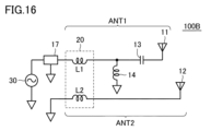
- FIG. 16 is a circuit diagram of an antenna device 100B in Modification 2. As shown in FIG. In antenna device 100B shown in FIG. 16, the same components as those of antenna device 100 shown in FIG. 1 are denoted by the same reference numerals, and detailed description thereof will not be repeated.
- the antenna device 100B includes a first antenna ANT1 and a second antenna ANT2.
- the first antenna ANT1 includes a first radiating element 11 connected to the feeding circuit 30 and a first coil L1 connected between the first radiating element 11 and the feeding circuit.
- the second antenna ANT2 includes a second coil L2 magnetically coupled to the first coil L1, and a second radiation element 12 connected to the second coil L2.
- the antenna device 100B has an impedance matching element 17 connected between the first coil L1 and the first radiation element 11 .
- the impedance matching element 17 in the first antenna ANT1 By providing the impedance matching element 17 in the first antenna ANT1, the current flowing through the first coil L1 (transformer primary side) at the resonance frequency of the fundamental wave of the second antenna ANT2 can be divided by the impedance matching element 17. By shunting the current flowing through the first coil L1 (primary side of the transformer), the amount of current flowing through the second antenna ANT2 can be made smaller at the resonance frequency of the fundamental wave of the second antenna ANT2.
- the impedance matching element 17 is a part of the first antenna ANT1, and the impedance of the first antenna ANT1 is measured with the impedance matching element 17 included.
- the antenna device 100B according to Modification 2 further includes the impedance matching element 17 (first impedance matching element) connected between the first coil L1 and the feeding circuit 30. Accordingly, the antenna device 100B according to Modification 2 can further reduce the amount of current flowing through the second antenna ANT2 at the resonance frequency of the fundamental wave of the second antenna ANT2.
- FIG. 17 is a circuit diagram of an antenna device 100C in Modification 3. As shown in FIG. In antenna device 100C shown in FIG. 17, the same components as those of antenna device 100 shown in FIG. 1 are denoted by the same reference numerals, and detailed description thereof will not be repeated.
- the antenna device 100C includes a first antenna ANT1 and a second antenna ANT2.
- the first antenna ANT1 includes a first radiating element 11 connected to the feeding circuit 30 and a first coil L1 connected between the first radiating element 11 and the feeding circuit.
- the second antenna ANT2 includes a second coil L2 magnetically coupled to the first coil L1, and a second radiation element 12 connected to the second coil L2. Furthermore, the antenna device 100C connects the capacitor 18 in parallel with the first coil L1.
- the capacitor 18 By connecting the capacitor 18 in parallel to the first coil L1, when the second antenna ANT2 is resonated at the resonance frequency of the third harmonic, the signal of the resonance frequency of the fifth harmonic or higher is sent to the transformer (first coil L1). It can be bypassed without going through the coil L1). As a result, it is possible to prevent the second antenna ANT2 from resonating at unnecessary resonance frequencies equal to or higher than the fifth harmonic.
- the antenna device 100C according to Modification 3 further includes the capacitor 18 that is connected in parallel with the first coil L1.
- the antenna device 100C according to Modification 3 can prevent the second antenna ANT2 from resonating at unnecessary resonance frequencies equal to or higher than the fifth harmonic.
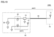
- FIG. 18 is a circuit diagram of an antenna device 100D in Modification 4. As shown in FIG. In antenna device 100D shown in FIG. 18, the same components as those of antenna device 100 shown in FIG. 1 are denoted by the same reference numerals, and detailed description thereof will not be repeated.
- the first radiating element 11 and the second radiating element 12 are not formed on the same substrate, and the first radiating element 11 is formed on a sub substrate 70 different from the main substrate 60 on which the second radiating element 12 is provided. 11 are formed.
- the main substrate 60 includes a power supply circuit 30 connected to the first radiation element 11, a first coil L1 connected between the first radiation element 11 and the power supply circuit, and a magnetically coupled circuit for the first coil L1. and a second radiation element 12 connected to the second coil L2.
- the first coil L1 and the second coil L2 constitute an antenna coupling element 20. As shown in FIG.
- the first radiation element 11 formed on the sub-board 70 and the first coil L1 formed on the main board 60 are connected by a coaxial cable 80 .
- the degree of freedom in arranging the first radiating element 11 is increased.
- the second radiation element 12, which is a parasitic element is formed on the main substrate 60, the second radiation element 12 can radiate radio waves from the second coil L2 without passing through a long transmission line. can be done. Therefore, transmission loss can be reduced in the second radiation element 12 .
- the transmission line that connects the main board 60 and the sub-board 70 is not limited to the coaxial cable 80, and may be a printed circuit board (PCB), a flexible printed circuit board (FPC), or a MetroCirc (registered trademark). and so on.
- Metrocirc (registered trademark) is a resin multilayer substrate in which multiple sheets of liquid crystal polymer (LCP) are laminated.
- the first radiation element 11 and the first coil L1 are connected by the coaxial cable 80, and the first radiation element 11 can be formed on the sub-board 70.
- the main substrate 60 and the sub-substrate 70 are examples, and the substrates forming the first radiation element 11 and the substrates forming the second radiation element 12 may be different substrates.
- FIG. 19 is a circuit diagram of an antenna device 100E in Modification 5. As shown in FIG. In antenna device 100E shown in FIG. 19, the same components as those of antenna device 100 shown in FIG. 1 and antenna device 100D shown in FIG. 18 are denoted by the same reference numerals, and detailed description thereof will not be repeated.
- the impedance matching element 19 is connected between the first coil L1 and the connection point of the coaxial cable 80.
- the impedance matching element 19 third impedance matching element
- the first antenna ANT1 is resonated at the resonance frequency of the fundamental wave
- the second antenna ANT2 is resonated at the triple harmonic resonance frequency.
- the present invention is not limited to this, and the antenna device 100 may resonate the first antenna ANT1 at the third harmonic resonance frequency and the second antenna ANT2 at the third harmonic resonance frequency.
- the first antenna ANT1 may also be caused to resonate at the resonance frequency of the fundamental wave.
- the antenna device 100 can also use the frequency band including the resonance frequency of the fundamental wave of the first antenna ANT1.
- the antenna device 100 may resonate the second antenna ANT2 at a resonance frequency other than the third harmonic.
- the length of the radiating element increases as the resonance frequency decreases. Therefore, if the second antenna ANT2 is resonated at the resonance frequency of the harmonic higher than three times, the resonance frequency of the fundamental wave becomes lower, so the length of the second radiating element 12 can be made longer. .
- the antenna device 100 is configured to excite the second antenna ANT2 in a higher frequency band including n79 with respect to the first antenna ANT1 that is excited in the band including n78.
- the antenna device 100 may be configured to excite the second antenna ANT2 in a lower frequency band than the first antenna ANT1 that excites in the band including n78.
- the antenna coupling element 20 may be additive or depolar.
Abstract
Provided are: an antenna device with which a frequency band to be used can be widened and sufficient radiation efficiency can be obtained; and a communication terminal device. According to the present disclosure, an antenna device (100) comprises: a first antenna (ANT1); and a second antenna (ANT2). The first antenna (ANT1) includes: a first radiation element (11) that is connected to a power feeding circuit (30) which supplies a high-frequency signal; and a first coil (L1) that is connected between the first radiation element (11) and the power feeding circuit (30). The second antenna (ANT2) includes: a second coil (L2) that is magnetically coupled to the first coil (L1); and a second radiation element (12) that is connected to the second coil (L2). The impedance of the first antenna (ANT1) is greater than 50 Ω in a resonance frequency of a fundamental wave of the second antenna (ANT2).
Description
本開示は、アンテナ装置、および通信端末装置の技術に関する。
The present disclosure relates to technology of antenna devices and communication terminal devices.
近年、複数の周波数帯域で動作させる通信端末装置が開発されている。当該通信端末装置に用いられるアンテナ装置は、使用可能な周波数帯域を広帯域化する必要があり直接的又は間接的に結合する2つのアンテナを備えている。給電するアンテナと無給電のアンテナとの2つのアンテナを結合させたアンテナ装置が特許文献1に示されている。
In recent years, communication terminal devices that operate in multiple frequency bands have been developed. An antenna device used in the communication terminal device is required to widen the usable frequency band and includes two antennas that are directly or indirectly coupled. Patent Document 1 discloses an antenna device in which two antennas, a fed antenna and a parasitic antenna, are coupled.
特許文献1に示すアンテナ装置において、例えば、LTE(Long Term Evolution)で使用されるLow-Band(0.7~0.96GHz)で用いる場合、共振周波数がそれ程高くないため十分なアンテナの長さ(放射素子の長さ)を確保することができる。
In the antenna device shown in Patent Document 1, for example, when used in Low-Band (0.7 to 0.96 GHz) used in LTE (Long Term Evolution), the resonance frequency is not so high, so the length of the antenna is sufficient (the length of the radiating element) can be ensured.
しかし、アンテナの長さは、共振周波数が高くなるほど短くなる。そのため、例えば、第5世代移動通信システム(5G)で使用する周波数帯域(3.3~5.0GHz)に用いる場合、アンテナ装置では、無給電のアンテナの長さが短くなり、十分な放射効率が得られないことがあった。
However, the length of the antenna becomes shorter as the resonance frequency becomes higher. Therefore, for example, when used in the frequency band (3.3 to 5.0 GHz) used in the 5th generation mobile communication system (5G), the antenna device has a short parasitic antenna length and sufficient radiation efficiency. could not be obtained.
本開示は、このような課題を解決するためになされたものであり、その目的は使用する周波数帯域を広帯域化しつつ、十分な放射効率が得られるアンテナ装置、および通信端末装置を提供することである。
The present disclosure has been made to solve such problems, and its object is to provide an antenna device and a communication terminal device that can obtain sufficient radiation efficiency while widening the frequency band to be used. be.
本開示に従うアンテナ装置は、第1アンテナと第2アンテナとを備えるアンテナ装置である。第1アンテナは、高周波信号を供給する給電回路に接続される第1放射素子と、第1アンテナと給電回路との間に接続される第1コイルと、を含む。第2アンテナは、第1コイルに対して磁気結合する第2コイルと、第2コイルに接続される第2放射素子と、を含む。第1アンテナのインピーダンスは、第2アンテナの基本波の共振周波数において、50Ωより大きい。
An antenna device according to the present disclosure is an antenna device comprising a first antenna and a second antenna. The first antenna includes a first radiating element connected to a feeding circuit that supplies a high frequency signal, and a first coil connected between the first antenna and the feeding circuit. The second antenna includes a second coil magnetically coupled to the first coil and a second radiating element connected to the second coil. The impedance of the first antenna is greater than 50Ω at the resonant frequency of the fundamental wave of the second antenna.
本開示に従う通信端末装置は、給電回路と、上記のアンテナ装置と、を備える。
A communication terminal device according to the present disclosure includes a feeding circuit and the antenna device described above.
本開示によるアンテナ装置においては、第1アンテナのインピーダンスが、第2アンテナの基本波の共振周波数において、50Ωより大きいので、使用する周波数帯域を広帯域化することができるとともに、十分な放射効率が得られる。
In the antenna device according to the present disclosure, since the impedance of the first antenna is greater than 50Ω at the resonance frequency of the fundamental wave of the second antenna, the frequency band to be used can be widened and sufficient radiation efficiency can be obtained. be done.
以下、本開示の実施の形態について、図面を参照しながら詳細に説明する。なお、図中同一または相当部分には同一符号を付してその説明は繰り返さない。
Hereinafter, embodiments of the present disclosure will be described in detail with reference to the drawings. The same or corresponding parts in the drawings are denoted by the same reference numerals, and the description thereof will not be repeated.
[実施の形態]
図1は、実施の形態におけるアンテナ装置100の回路図である。アンテナ装置100は、第1アンテナANT1と第2アンテナANT2とを備える。第1アンテナANT1は、給電回路30に接続される第1放射素子11と、第1放射素子11と給電回路との間に接続される第1コイルL1と、を含む。第2アンテナANT2は、第1コイルL1に対して磁気結合する第2コイルL2と、第2コイルL2に接続される第2放射素子12と、を含む。そのため、第1アンテナANT1は、給電回路30により給電される給電アンテナで、第2アンテナANT2は、給電回路30と接続されておらず、給電回路30により給電されない無給電アンテナである。 [Embodiment]
FIG. 1 is a circuit diagram of anantenna device 100 according to an embodiment. The antenna device 100 includes a first antenna ANT1 and a second antenna ANT2. The first antenna ANT1 includes a first radiating element 11 connected to the feeding circuit 30 and a first coil L1 connected between the first radiating element 11 and the feeding circuit. The second antenna ANT2 includes a second coil L2 magnetically coupled to the first coil L1, and a second radiation element 12 connected to the second coil L2. Therefore, the first antenna ANT1 is a fed antenna that is fed by the feeding circuit 30, and the second antenna ANT2 is not connected to the feeding circuit 30 and is a parasitic antenna that is not fed by the feeding circuit 30.
図1は、実施の形態におけるアンテナ装置100の回路図である。アンテナ装置100は、第1アンテナANT1と第2アンテナANT2とを備える。第1アンテナANT1は、給電回路30に接続される第1放射素子11と、第1放射素子11と給電回路との間に接続される第1コイルL1と、を含む。第2アンテナANT2は、第1コイルL1に対して磁気結合する第2コイルL2と、第2コイルL2に接続される第2放射素子12と、を含む。そのため、第1アンテナANT1は、給電回路30により給電される給電アンテナで、第2アンテナANT2は、給電回路30と接続されておらず、給電回路30により給電されない無給電アンテナである。 [Embodiment]
FIG. 1 is a circuit diagram of an
給電される第1アンテナANT1には、直列に接続されるコンデンサ13と、一端が接続されるコイル14とが設けてある。コイル14の他端は、GNDに接続されている。コンデンサ13およびコイル14はLC回路を構成し、第1アンテナANT1のフィルタ回路として機能している。なお、第1アンテナANT1においてフィルタ回路が不要であれば、コンデンサ13およびコイル14を設ける必要はない。
A first antenna ANT1 to which power is supplied is provided with a capacitor 13 connected in series and a coil 14 to which one end is connected. The other end of the coil 14 is connected to GND. A capacitor 13 and a coil 14 form an LC circuit and function as a filter circuit for the first antenna ANT1. Note that if the filter circuit is unnecessary in the first antenna ANT1, the capacitor 13 and the coil 14 need not be provided.
アンテナ装置100では、使用可能な周波数帯域を広帯域化するために第1アンテナANT1と第2アンテナANT2とを、第1コイルL1と第2コイルL2とで磁気結合している。つまり、第1コイルL1と第2コイルL2とは、アンテナ結合素子20を構成している。
In the antenna device 100, the first antenna ANT1 and the second antenna ANT2 are magnetically coupled by the first coil L1 and the second coil L2 in order to widen the usable frequency band. That is, the first coil L1 and the second coil L2 constitute the antenna coupling element 20. As shown in FIG.
アンテナ結合素子20は、電子機器内の回路基板に実装される、直方体状のチップ部品である。例えば、アンテナ結合素子20を樹脂多層基板で構成する場合、アンテナ結合素子20は、絶縁基材に液晶ポリマー(LCP[Liquid Crystal Polymer])シートを用いて、銅箔で第1コイルL1および第2コイルL2の導体パターンをパターンニングした各々の絶縁基材を積層することで構成される。また、例えば、アンテナ結合素子20をセラミック多層基板で構成する場合、アンテナ結合素子20は、絶縁基材に低温同時焼成セラミックス(LTCC[Low Temperature Co-fired Ceramics])を用いて、銅ペーストを印刷形成して第1コイルL1および第2コイルL2の導体パターンをパターンニングした各々の絶縁基材を積層することで構成される。さらに、アンテナ結合素子20は、セラミック多層基板に限らず、例えば、ガラスを主成分とした絶縁ペーストのスクリーン印刷による塗布を繰り返すことで形成してもよい。このように、アンテナ結合素子20は、絶縁基材が非磁性体であることにより(磁性体フェライトではないので)、所定インダクタンス、所定結合係数のトランスとして用いることができる。
The antenna coupling element 20 is a rectangular parallelepiped chip part mounted on a circuit board in an electronic device. For example, when the antenna coupling element 20 is configured with a resin multilayer substrate, the antenna coupling element 20 uses a liquid crystal polymer (LCP [Liquid Crystal Polymer]) sheet as the insulating base material, and copper foil is used to form the first coil L1 and the second coil L1. It is constructed by laminating each insulating base material on which the conductor pattern of the coil L2 is patterned. Also, for example, when the antenna coupling element 20 is composed of a ceramic multilayer substrate, the antenna coupling element 20 uses low temperature co-fired ceramics (LTCC [Low Temperature Co-fired Ceramics]) for the insulating base material, and copper paste is printed. It is configured by laminating respective insulating base materials formed and patterned with conductor patterns of the first coil L1 and the second coil L2. Furthermore, the antenna coupling element 20 is not limited to the ceramic multilayer substrate, and may be formed by, for example, repeatedly applying an insulating paste containing glass as a main component by screen printing. As described above, the antenna coupling element 20 can be used as a transformer with a predetermined inductance and a predetermined coupling coefficient because the insulating base material is non-magnetic (not magnetic ferrite).
このように、アンテナ装置100は、二つの放射素子(第1放射素子11および第2放射素子12)を、アンテナ結合素子20を接続することで、広帯域をカバーすることができる。ところが、例えば、第5世代移動通信システム(5G)で使用する周波数帯域(3.3~5.0GHz)や5GHz帯の無線LANなどの周波数帯域をアンテナ装置100でカバーする場合、第2アンテナANT2を高い共振周波数で共振させる必要があり、第2放射素子12の長さが短くなる。しかし、第2放射素子12の長さが短くなると、十分な放射効率が得られない場合があった。
Thus, the antenna device 100 can cover a wide band by connecting two radiation elements (the first radiation element 11 and the second radiation element 12) to the antenna coupling element 20. However, for example, when the antenna device 100 covers the frequency band (3.3 to 5.0 GHz) used in the fifth generation mobile communication system (5G) or the frequency band such as the 5 GHz band wireless LAN, the second antenna ANT2 is required to resonate at a high resonance frequency, and the length of the second radiating element 12 is shortened. However, when the length of the second radiation element 12 is shortened, sufficient radiation efficiency may not be obtained.
そこで、第2アンテナANT2を基本波の共振周波数で共振させるのではなく高調波の共振周波数で共振させることで、第2放射素子12の長さを長くすることができる。つまり、第2アンテナANT2で共振させたい共振周波数が例えば4.4GHzである場合に、4.4GHzの基本波で第2アンテナANT2を共振させる場合、第2放射素子12の長さは短くなる。しかし、4.4GHzの3倍高調波で第2アンテナANT2を共振させる場合、基本波の共振周波数は1.4GHzとなる。第2放射素子12の長さを1.4GHzの基本波の共振周波数で規定することで、4.4GHzの基本波の共振周波数で規定した場合に比べ、放射素子の長さを長くすることができる。アンテナ装置100では、第2アンテナANT2を高調波の共振周波数で共振させることで第2放射素子12の長さを長くして、十分な放射効率を得ることができる。
Therefore, the length of the second radiation element 12 can be lengthened by resonating the second antenna ANT2 not at the resonant frequency of the fundamental wave but at the resonant frequency of the harmonic wave. That is, when the resonance frequency to be resonated in the second antenna ANT2 is, for example, 4.4 GHz, the length of the second radiation element 12 is shortened when the second antenna ANT2 is resonated with the fundamental wave of 4.4 GHz. However, when resonating the second antenna ANT2 with the triple harmonic of 4.4 GHz, the resonance frequency of the fundamental wave is 1.4 GHz. By defining the length of the second radiating element 12 with the resonant frequency of the fundamental wave of 1.4 GHz, the length of the radiating element can be made longer than when the length of the second radiating element 12 is defined with the resonant frequency of the fundamental wave of 4.4 GHz. can. In the antenna device 100, the length of the second radiation element 12 is lengthened by causing the second antenna ANT2 to resonate at the resonant frequency of the harmonic, and sufficient radiation efficiency can be obtained.
具体的に、第1放射素子11および第2放射素子12の長さについて説明する。図2は、実施の形態における通信端末装置を示す概略図である。図2に示す通信端末装置は、n78(3.3-3.8GHz)を含む帯域およびn79(4.4-4.9GHz)を含む帯域で通信が可能な携帯端末200である。そのため、携帯端末200は、n78を含む帯域で励起される第1アンテナANT1と、n79を含む帯域で励起される第2アンテナANT2とを含むアンテナ装置100が設けてある。なお、携帯端末200は、例えば、携帯電話、スマートフォンあるいはタブレットなどである。
Specifically, the lengths of the first radiation element 11 and the second radiation element 12 will be described. FIG. 2 is a schematic diagram showing a communication terminal device according to the embodiment. The communication terminal device shown in FIG. 2 is a mobile terminal 200 capable of communication in a band including n78 (3.3-3.8 GHz) and a band including n79 (4.4-4.9 GHz). Therefore, mobile terminal 200 is provided with antenna device 100 including first antenna ANT1 excited in a band including n78 and second antenna ANT2 excited in a band including n79. Note that the mobile terminal 200 is, for example, a mobile phone, a smart phone, a tablet, or the like.
アンテナ装置100は、第1放射素子11および第2放射素子12がパターニングされた基板210の裏側にアンテナ結合素子20が設けてあり、第1アンテナANT1と第2アンテナANT2とを結合している。また、第1アンテナANT1は、図示していないが配線で給電回路30に対して電気的に接続されているが、第2アンテナANT2は、給電回路30に対して電気的に接続されていない。
The antenna device 100 has an antenna coupling element 20 provided on the back side of a substrate 210 on which the first radiation element 11 and the second radiation element 12 are patterned, and couples the first antenna ANT1 and the second antenna ANT2. Also, although the first antenna ANT1 is electrically connected to the feeding circuit 30 by wiring (not shown), the second antenna ANT2 is not electrically connected to the feeding circuit 30. FIG.
図2に示すように、第1放射素子11はアンテナ結合素子20から図中左方向に延びる線状の導体パターンで構成されている。また、第2放射素子12は、アンテナ結合素子20から図中右方向に延び、途中で図中左方向へ折り返す線状の導体パターンで構成されている。第1放射素子11および第2放射素子12はいずれもモノポールアンテナとして作用する。
As shown in FIG. 2, the first radiation element 11 is composed of a linear conductor pattern extending from the antenna coupling element 20 in the left direction in the drawing. The second radiating element 12 is composed of a linear conductor pattern that extends from the antenna coupling element 20 in the right direction in the drawing and turns back in the left direction in the middle. Both the first radiating element 11 and the second radiating element 12 act as a monopole antenna.
第1アンテナANT1はn78を含む帯域で励起され、第2アンテナANT2はn79含む帯域で励起されるので、ともに基本波の共振周波数で共振させるのであれば放射素子の長さは、第2放射素子12より第1放射素子11の方が長くなる。しかし、第2アンテナANT2は、3倍高調波の共振周波数で共振させるため、図2に示すように放射素子の長さは、第1放射素子11より第2放射素子12の方が長くなっている。
The first antenna ANT1 is excited in a band including n78, and the second antenna ANT2 is excited in a band including n79. First radiating element 11 is longer than 12 . However, since the second antenna ANT2 resonates at the third harmonic resonance frequency, the length of the radiation element is longer in the second radiation element 12 than in the first radiation element 11, as shown in FIG. there is
第2アンテナANT2を高調波の共振周波数で共振させる場合であっても、第2アンテナANT2は、基本波の共振周波数で共振される。アンテナ装置100が対象としている周波数帯域に第2アンテナANT2の基本波の共振周波数が含まれていない場合、第2アンテナANT2が基本波の共振周波数で共振すると、アンテナ装置100としては、対象としている周波数帯域以外の妨害波を受信することになり通信性能が劣化する。
Even when the second antenna ANT2 is resonated at the harmonic resonance frequency, the second antenna ANT2 is resonated at the fundamental resonance frequency. When the resonance frequency of the fundamental wave of the second antenna ANT2 is not included in the frequency band targeted by the antenna device 100, and the second antenna ANT2 resonates at the resonance frequency of the fundamental wave, the antenna device 100 Interfering waves outside the frequency band are received, and communication performance deteriorates.
そこで、アンテナ装置100は、第2アンテナANT2の基本波の共振周波数で共振しないようにインピーダンスの調整を行っている。具体的に、アンテナ装置100は、第1アンテナANT1のインピーダンスが、第2アンテナANT2の基本波の共振周波数において、例えば50Ωより大きくなるように調整する。50Ωという数字は一般的なアンテナ設計でも用いられる基準値であり、これよりインピーダンスが大きい場合は、回路に流れる電流値が減少する。また、一般的なアンテナ設計においては、給電回路30の入力側のインピーダンスも50Ω近傍に相当する。したがって、「対象のインピーダンスが50Ωより大きい」場合は、「対象のインピーダンスが給電回路30の入力側のインピーダンスより大きい」場合に相当する。また、本明細書において、インピーダンスの大きさの比較は、インピーダンスの実部と虚部を加味した絶対値で比較する。
Therefore, the antenna device 100 adjusts the impedance so as not to resonate at the resonance frequency of the fundamental wave of the second antenna ANT2. Specifically, the antenna device 100 adjusts the impedance of the first antenna ANT1 to be, for example, greater than 50Ω at the resonance frequency of the fundamental wave of the second antenna ANT2. The figure of 50Ω is a reference value that is also used in general antenna design, and if the impedance is higher than this, the current flowing through the circuit will decrease. Further, in a general antenna design, the impedance on the input side of the feeding circuit 30 also corresponds to around 50Ω. Therefore, the case where "the target impedance is greater than 50Ω" corresponds to the case where "the target impedance is greater than the impedance on the input side of the feeding circuit 30". Also, in this specification, the magnitude of impedance is compared with an absolute value that takes into consideration the real part and the imaginary part of impedance.
ここで、図3は、実施の形態における第1アンテナANT1のインピーダンスを測定する場合の構成を示す概略図である。第1アンテナANT1のインピーダンスの測定は、図3のように、給電回路30の代わりに第1コイルL1に対してネットワークアナライザ50を測定ケーブル51で繋ぎ、第1測定状態にして行う。このとき、第1コイルL1と第2コイルL2が一体的に素子に形成され分離が難しい場合、第2コイルL2から第2放射素子12およびGNDを外して第2コイルL2の両端をオープンにする。第1測定状態にして、第1コイルL1と測定ケーブル51と接続点を測定点t1としてネットワークアナライザ50で、第1アンテナANT1のインピーダンスの周波数特性を測定する。なお、測定ケーブル51の長さによる位相シフトについては、トランスの一次側である第1コイルL1との接続点であらかじめ校正しておく。
Here, FIG. 3 is a schematic diagram showing the configuration for measuring the impedance of the first antenna ANT1 according to the embodiment. The impedance of the first antenna ANT1 is measured by connecting the network analyzer 50 with the measurement cable 51 to the first coil L1 instead of the feeding circuit 30 as shown in FIG. At this time, if the first coil L1 and the second coil L2 are integrally formed into an element and it is difficult to separate them, the second radiation element 12 and GND are removed from the second coil L2 to open both ends of the second coil L2. . In the first measurement state, the frequency characteristic of the impedance of the first antenna ANT1 is measured by the network analyzer 50 with the connection point between the first coil L1 and the measurement cable 51 as the measurement point t1. The phase shift due to the length of the measurement cable 51 is calibrated in advance at the connection point with the first coil L1 on the primary side of the transformer.
また、図4は、実施の形態における第2アンテナANT2のインピーダンスを測定する場合の構成を示す概略図である。第2アンテナANT2の基本波の共振周波数の測定は、図4のように、GNDに接続する代わりに第2コイルL2に対してネットワークアナライザ50を測定ケーブル52で繋ぎ、第2測定状態にして行う。このとき、第1コイルL1と第2コイルL2が一体的に素子に形成され分離が難しい場合、第1コイルL1から第1放射素子11および給電回路30を外して第1コイルL1の両端をオープンにする。第2測定状態にして、第2コイルL2と測定ケーブル52と接続点を測定点t2としてネットワークアナライザ50で、第2アンテナANT2の基本波の周波数特性を測定する。この測定により、無給電素子の共振周波数を特定できる。なお、測定ケーブル52の長さによる位相シフトについては、トランスの二次側である第2コイルL2との接続点であらかじめ校正しておく。上記第1および第2測定状態での測定により、第2アンテナANT2の基本波の共振周波数における、第1アンテナANT1のインピーダンスを特定することができる。
Also, FIG. 4 is a schematic diagram showing a configuration for measuring the impedance of the second antenna ANT2 in the embodiment. Measurement of the resonance frequency of the fundamental wave of the second antenna ANT2 is performed in the second measurement state by connecting the network analyzer 50 to the second coil L2 with the measurement cable 52 instead of connecting to GND as shown in FIG. . At this time, if the first coil L1 and the second coil L2 are integrally formed as an element and it is difficult to separate them, the first radiation element 11 and the feeding circuit 30 are removed from the first coil L1, and both ends of the first coil L1 are opened. to In the second measurement state, the frequency characteristic of the fundamental wave of the second antenna ANT2 is measured by the network analyzer 50 with the connection point between the second coil L2 and the measurement cable 52 as the measurement point t2. This measurement allows the resonance frequency of the parasitic element to be identified. The phase shift due to the length of the measurement cable 52 is calibrated in advance at the connection point with the second coil L2 on the secondary side of the transformer. The impedance of the first antenna ANT1 at the resonance frequency of the fundamental wave of the second antenna ANT2 can be specified by the measurements in the first and second measurement states.
アンテナ装置100は、第2アンテナANT2の基本波の共振周波数において、第1アンテナANT1のインピーダンスが50Ωより大きいことで、第2アンテナANT2の基本波の共振周波数において、第1コイルL1(トランスの一次側)に流れる電流が減少する。そのため、第2コイルL2(トランスの二次側)に生じる誘導起電力も減少し、第2アンテナANT2自体は基本波の共振周波数で共振しても、アンテナ装置100全体としては、第2アンテナANT2の基本波の共振周波数で共振しなくなる。
Since the impedance of the first antenna ANT1 is greater than 50Ω at the resonance frequency of the fundamental wave of the second antenna ANT2, the antenna device 100 can achieve the first coil L1 (primary side) is reduced. Therefore, the induced electromotive force generated in the second coil L2 (secondary side of the transformer) is also reduced, and even if the second antenna ANT2 itself resonates at the resonance frequency of the fundamental wave, the antenna device 100 as a whole can will not resonate at the resonance frequency of the fundamental wave of
図5は、実施の形態におけるアンテナ装置100の反射係数の周波数特性を示す図である。図5において、横軸は周波数、縦軸は反射係数である。ここで、反射係数Aは図1において給電回路30からアンテナ結合素子20側を見た(つまりアンテナ装置100の)反射係数である。また、反射係数Bは図1において第1コイルL1から第1放射素子11側を見た(つまり、第1アンテナANT1の)反射係数である。
FIG. 5 is a diagram showing the frequency characteristics of the reflection coefficient of the antenna device 100 according to the embodiment. In FIG. 5, the horizontal axis is frequency and the vertical axis is reflection coefficient. Here, the reflection coefficient A is the reflection coefficient when the antenna coupling element 20 side is viewed from the feeding circuit 30 in FIG. 1 (that is, the reflection coefficient of the antenna device 100). A reflection coefficient B is a reflection coefficient of the first radiation element 11 side viewed from the first coil L1 in FIG. 1 (that is, of the first antenna ANT1).
反射係数Aにおいて、n78を含む帯域で第1アンテナANT1の基本波の共振周波数(第1コイルL1と第1放射素子11とによる共振周波数)で共振が生じ、n79を含む帯域で第2アンテナANT2による3倍高調波の共振周波数(例えば、4.8GHz)で共振が生じている。一方、反射係数Bにおいて、n78を含む帯域で第1アンテナANT1の基本波の共振周波数で共振が生じている。つまり、アンテナ装置100では、アンテナ結合素子20で第2アンテナANT2を第1アンテナANT1に結合させることで、n79を含む帯域まで広帯域化することができる。なお、アンテナ装置100は前述のようにインピーダンスの調整を行うことで、反射係数Aにおいて、第2アンテナANT2の基本波の共振周波数(例えば、1.5GHz)で共振が観測されていない。つまり、アンテナ装置100は、第2アンテナANT2の基本波の共振周波数において動作しない。
In the reflection coefficient A, resonance occurs at the resonance frequency of the fundamental wave of the first antenna ANT1 (the resonance frequency of the first coil L1 and the first radiation element 11) in the band including n78, and the second antenna ANT2 occurs in the band including n79. Resonance occurs at the resonance frequency (eg, 4.8 GHz) of the third harmonic due to . On the other hand, in the reflection coefficient B, resonance occurs at the resonance frequency of the fundamental wave of the first antenna ANT1 in the band including n78. That is, in the antenna device 100, by coupling the second antenna ANT2 to the first antenna ANT1 with the antenna coupling element 20, it is possible to widen the band up to the band including n79. By adjusting the impedance of the antenna device 100 as described above, no resonance is observed at the resonance frequency (for example, 1.5 GHz) of the fundamental wave of the second antenna ANT2 at the reflection coefficient A. That is, the antenna device 100 does not operate at the resonance frequency of the fundamental wave of the second antenna ANT2.
図6は、実施の形態におけるアンテナ装置100の放射効率を説明するための図である。図6において、横軸は周波数、縦軸は放射効率である。図6において、特性Cは第2アンテナANT2を3倍高調波の共振周波数で共振させた場合のアンテナ装置100の放射効率の周波数特性であり、特性Dは第2アンテナANT2を基本波の共振周波数で共振させた場合のアンテナ装置の放射効率の周波数特性である。第2アンテナANT2を3倍高調波の共振周波数で共振させた場合の方が、第2放射素子12の長さを長くすることができるので、アンテナ装置100は、特性Cが示すようにn79を含む帯域で放射効率が向上している。
FIG. 6 is a diagram for explaining the radiation efficiency of the antenna device 100 according to the embodiment. In FIG. 6, the horizontal axis is frequency and the vertical axis is radiation efficiency. In FIG. 6, the characteristic C is the frequency characteristic of the radiation efficiency of the antenna device 100 when the second antenna ANT2 is resonated at the resonance frequency of the third harmonic, and the characteristic D is the frequency characteristic of the second antenna ANT2 at the resonance frequency of the fundamental wave. 4 shows the frequency characteristics of the radiation efficiency of the antenna device when resonating at . Since the length of the second radiation element 12 can be increased when the second antenna ANT2 is resonated at the resonance frequency of the third harmonic, the antenna device 100 can reduce n79 as indicated by the characteristic C. The radiation efficiency is improved in the band including.
次に、第2アンテナANT2の基本波の共振周波数においてアンテナ装置100を動作させないインピーダンスの調整について説明する。図7は、実施の形態におけるアンテナ装置100のインピーダンスを第1状態に調整した場合のスミスチャートを示す図である。図8は、実施の形態におけるアンテナ装置100のインピーダンスを第1状態に調整した場合のアンテナ特性を説明するための図である。
Next, the impedance adjustment that does not operate the antenna device 100 at the resonance frequency of the fundamental wave of the second antenna ANT2 will be described. FIG. 7 is a Smith chart when the impedance of the antenna device 100 according to the embodiment is adjusted to the first state. FIG. 8 is a diagram for explaining antenna characteristics when the impedance of the antenna device 100 according to the embodiment is adjusted to the first state.
図7に示すスミスチャートは、図1に示すアンテナ装置100の第1コイルL1と第1放射素子11との間に移相器(図示せず)を設けて第1アンテナANT1のインピーダンスを第1状態に調整した場合を図示している。ここで、第1状態とは、移相器により、第1測定状態で給電回路30から見込む、第1アンテナANT1の反射係数の位相が180度付近である状態である。反射係数の位相とは、スミスチャートにおいて中心から右側のX軸を起点として、反時計回りに、対象周波数の点と中心とを結んだ線とのなす角度である。
In the Smith chart shown in FIG. 7, a phase shifter (not shown) is provided between the first coil L1 and the first radiation element 11 of the antenna device 100 shown in FIG. The figure shows a case in which the state is adjusted. Here, the first state is a state in which the phase of the reflection coefficient of the first antenna ANT1 seen from the feeding circuit 30 in the first measurement state is around 180 degrees due to the phase shifter. The phase of the reflection coefficient is the angle formed by the line connecting the point of the target frequency and the center in the counterclockwise direction starting from the X-axis on the right side of the center of the Smith chart.
同様に、図9は、実施の形態におけるアンテナ装置100のインピーダンスを第2状態に調整した場合のスミスチャートを示す図である。図10は、実施の形態におけるアンテナ装置100のインピーダンスを第2状態に調整した場合のアンテナ特性を説明するための図である。ここで、第2状態とは、移相器により、第1測定状態で給電回路30から見込む、第1アンテナANT1の反射係数の位相が90度付近にある状態である。また、電圧と電流の位相差は90度付近にある状態でもある。
Similarly, FIG. 9 is a diagram showing a Smith chart when the impedance of the antenna device 100 according to the embodiment is adjusted to the second state. FIG. 10 is a diagram for explaining antenna characteristics when the impedance of the antenna device 100 according to the embodiment is adjusted to the second state. Here, the second state is a state in which the phase of the reflection coefficient of the first antenna ANT1 seen from the feeding circuit 30 in the first measurement state is near 90 degrees due to the phase shifter. Also, the phase difference between the voltage and the current is in the vicinity of 90 degrees.
図11は、実施の形態におけるアンテナ装置100のインピーダンスを第3状態に調整した場合のスミスチャートを示す図である。図12は、実施の形態におけるアンテナ装置100のインピーダンスを第3状態に調整した場合のアンテナ特性を説明するための図である。ここで、第3状態とは、移相器により、第1測定状態で給電回路30から見込む、第1アンテナANT1の反射係数の位相が0(ゼロ)度付近にある状態である。また、電圧と電流の位相差は180度付近にある状態でもある。
FIG. 11 is a Smith chart when the impedance of the antenna device 100 according to the embodiment is adjusted to the third state. FIG. 12 is a diagram for explaining antenna characteristics when the impedance of the antenna device 100 according to the embodiment is adjusted to the third state. Here, the third state is a state in which the phase of the reflection coefficient of the first antenna ANT1 seen from the feeding circuit 30 in the first measurement state is near 0 (zero) degrees due to the phase shifter. Also, the phase difference between voltage and current is in the vicinity of 180 degrees.
図13は、実施の形態におけるアンテナ装置100のインピーダンスを第4状態に調整した場合のスミスチャートを示す図である。図14は、実施の形態におけるアンテナ装置100のインピーダンスを第4状態に調整した場合のアンテナ特性を説明するための図である。ここで、第4状態とは、移相器により、第1測定状態で給電回路30から見込む、第1アンテナANT1の反射係数の位相が-90度付近にある状態である。また、電圧と電流の位相差は-90度付近にある状態でもある。
FIG. 13 is a Smith chart when the impedance of the antenna device 100 according to the embodiment is adjusted to the fourth state. FIG. 14 is a diagram for explaining antenna characteristics when the impedance of the antenna device 100 according to the embodiment is adjusted to the fourth state. Here, the fourth state is a state in which the phase of the reflection coefficient of the first antenna ANT1 seen from the feeding circuit 30 in the first measurement state is near -90 degrees due to the phase shifter. Also, the phase difference between the voltage and the current is in the vicinity of -90 degrees.
なお、図7~図14では、第1アンテナANT1のインピーダンスとアンテナ装置100の特性との関係を説明するために、アンテナ装置100に移相器を設けて、第1アンテナANT1のインピーダンスを変化させている。しかし、実施の形態におけるアンテナ装置100には必ずしも移相器を設ける必要はない。つまり、実施の形態におけるアンテナ装置100では、第2放射素子12の基本波の共振周波数において動作しないように回路構成でインピーダンスを調整すれば移相器を設けなくても良い。
7 to 14, in order to explain the relationship between the impedance of the first antenna ANT1 and the characteristics of the antenna device 100, the antenna device 100 is provided with a phase shifter to change the impedance of the first antenna ANT1. ing. However, the antenna device 100 in the embodiment does not necessarily need to be provided with a phase shifter. In other words, in the antenna device 100 according to the embodiment, if the impedance is adjusted in the circuit configuration so as not to operate at the resonance frequency of the fundamental wave of the second radiation element 12, the phase shifter need not be provided.
第2アンテナANT2の基本波の共振周波数における、第1アンテナANT1のインピーダンスの変化を表1に示す。表1では、反射係数の位相(差)を180度、90度、0度、-90度と変化させた場合の第1アンテナANT1のインピーダンスの変化を示している。なお、表1では、Re{Z}がインピーダンスの実部を、Im{Z}がインピーダンスの虚部をそれぞれ示している。また、表1では、給電回路30の入力側のインピーダンスがいずれも50.0Ωである。インピーダンスの大きさの比較は、インピーダンスの実部と虚部を加味した絶対値で比較する。
Table 1 shows changes in the impedance of the first antenna ANT1 at the resonance frequency of the fundamental wave of the second antenna ANT2. Table 1 shows changes in the impedance of the first antenna ANT1 when the phase (difference) of the reflection coefficients is changed to 180 degrees, 90 degrees, 0 degrees, and -90 degrees. In Table 1, Re{Z} represents the real part of impedance, and Im{Z} represents the imaginary part of impedance. Also, in Table 1, the impedance on the input side of the feeding circuit 30 is 50.0Ω. The magnitude of the impedance is compared with the absolute value considering the real part and the imaginary part of the impedance.

図7(a),図9(a),図11(a),図13(a)は、第2アンテナANT2を結合させない第1アンテナANT1単体を第1放射素子11側から見たインピーダンスをスミスチャート上に軌跡として表した図である。マークm1は、第2アンテナANT2の基本波の共振周波数における第1アンテナANT1のインピーダンスを示している。図7(a),図9(a),図11(a),図13(a)に示すように、反射係数の位相差が180度、90度、0度、-90度と変化させるに従い、マークm1が時計回りに移動している。図7(a),図9(a),図11(a),図13(a)に示すスミスチャートは、50Ωで正規化されているため、反射係数の位相差90度以下、-90度以上で第1アンテナANT1のインピーダンスが50Ωより大きくなる。すなわち、スミスチャートで対象周波数における点が右半分に存在する場合は第1アンテナANT1のインピーダンスが50Ωより大きくなる。
7(a), 9(a), 11(a), and 13(a) show the impedance of the first antenna ANT1, which is not coupled to the second antenna ANT2, viewed from the first radiation element 11 side. It is a figure represented as a locus|trajectory on a chart. A mark m1 indicates the impedance of the first antenna ANT1 at the resonance frequency of the fundamental wave of the second antenna ANT2. As shown in FIGS. 7(a), 9(a), 11(a), and 13(a), as the phase difference of the reflection coefficient changes from 180 degrees, 90 degrees, 0 degrees, and −90 degrees, , the mark m1 is moving clockwise. The Smith charts shown in FIGS. 7(a), 9(a), 11(a), and 13(a) are normalized by 50 Ω, so the phase difference of the reflection coefficient is 90 degrees or less, −90 degrees Thus, the impedance of the first antenna ANT1 becomes greater than 50Ω. That is, when the point at the target frequency exists in the right half of the Smith chart, the impedance of the first antenna ANT1 is greater than 50Ω.
図7(b),図9(b),図11(b),図13(b)は、第2アンテナANT2を結合させたアンテナ装置100全体を給電回路30側から見たインピーダンスをスミスチャート上に軌跡として表した図である。マークm2は、第2アンテナANT2の基本波の共振周波数におけるアンテナ装置100全体のインピーダンスを示している。図7(b),図9(b),図11(b),図13(b)に示すように、反射係数の位相差が180度、90度、0度、-90度と変化させるに従い、マークm2が時計回りに移動している。図7(b),図9(b),図11(b),図13(b)に示すスミスチャートは、50Ωで正規化されているため、位相差90度以下、270度以上でアンテナ装置100全体のインピーダンスが50Ωより大きくなる。すなわち、スミスチャートで対象周波数における点が右半分に存在する場合は、アンテナ装置100全体のインピーダンスが50Ωより大きくなる。
7(b), 9(b), 11(b), and 13(b) show the impedance of the entire antenna device 100 coupled with the second antenna ANT2 as seen from the feeding circuit 30 side on the Smith chart. 2 is a diagram represented as a trajectory in FIG. A mark m2 indicates the impedance of the entire antenna device 100 at the resonance frequency of the fundamental wave of the second antenna ANT2. As shown in FIGS. 7(b), 9(b), 11(b), and 13(b), as the phase difference of the reflection coefficient changes from 180 degrees, 90 degrees, 0 degrees, and -90 degrees, , the mark m2 is moving clockwise. Since the Smith charts shown in FIGS. 7(b), 9(b), 11(b), and 13(b) are normalized by 50Ω, the antenna device can The overall impedance of 100 is greater than 50Ω. That is, when the point at the target frequency exists in the right half of the Smith chart, the impedance of the entire antenna device 100 is greater than 50Ω.
図8(a),図10(a),図12(a),図14(a)は、反射係数の位相差を180度、90度、0度、-90度と変化させた場合のアンテナ装置100の反射係数の周波数特性を示す図である。図8(a),図10(a),図12(a),図14(a)において、横軸は周波数、縦軸は反射係数である。マークm3は、第2アンテナANT2の基本波の共振周波数におけるアンテナ装置100の反射係数のピークを示している。マークm3に示す反射係数のピークは、位相差が180度、90度、0度と変化するに従い小さくなり、位相差が0度、-90度と変化するに従い大きくなる。
8(a), 10(a), 12(a), and 14(a) show the antenna when the phase difference of the reflection coefficient is changed to 180 degrees, 90 degrees, 0 degrees, and -90 degrees. FIG. 4 is a diagram showing the frequency characteristics of the reflection coefficient of the device 100; In FIGS. 8(a), 10(a), 12(a) and 14(a), the horizontal axis is the frequency and the vertical axis is the reflection coefficient. A mark m3 indicates the peak of the reflection coefficient of the antenna device 100 at the resonance frequency of the fundamental wave of the second antenna ANT2. The peak of the reflection coefficient indicated by the mark m3 decreases as the phase difference changes from 180 degrees, 90 degrees, and 0 degrees, and increases as the phase difference changes from 0 degrees to -90 degrees.
図8(b),図10(b),図12(b),図14(b)は、反射係数の位相差を180度、90度、0度、-90度と変化させた場合のアンテナ装置100に流れる電流量の周波数特性を示す図である。図8(b),図10(b),図12(b),図14(b)において、横軸は周波数、縦軸は電流量である。特性Eは第1アンテナANT1に流れる電流量の周波数特性であり、特性Fは第2アンテナANT2に流れる電流量の周波数特性であり、特性Gはアンテナ装置100全体に流れる電流量の周波数特性である。マークm4は、第2アンテナANT2の基本波の共振周波数における第2アンテナANT2に流れる電流量を示している。破線で囲まれている範囲が第2アンテナANT2の基本波の共振周波数の範囲である。マークm5は、第2アンテナANT2の3倍高調波の共振周波数における第2アンテナANT2に流れる電流量を示している。マークm4,m5に示す第2アンテナANT2に流れる電流量は、位相差が180度、90度、0度と変化するに従い小さくなり、位相差が0度、-90度と変化するに従い大きくなる。特に、反射係数の位相差が0(ゼロ)度の場合にマークm4に示す第2アンテナANT2に流れる電流量は略0(ゼロ)となっている。
8(b), 10(b), 12(b), and 14(b) show the antenna when the phase difference of the reflection coefficient is changed to 180 degrees, 90 degrees, 0 degrees, and -90 degrees. 4 is a diagram showing frequency characteristics of the amount of current flowing through the device 100. FIG. In FIGS. 8(b), 10(b), 12(b), and 14(b), the horizontal axis is the frequency and the vertical axis is the amount of current. Characteristic E is the frequency characteristic of the amount of current flowing through the first antenna ANT1, characteristic F is the frequency characteristic of the amount of current flowing through the second antenna ANT2, and characteristic G is the frequency characteristic of the amount of current flowing through the entire antenna device 100. . A mark m4 indicates the amount of current flowing through the second antenna ANT2 at the resonance frequency of the fundamental wave of the second antenna ANT2. The range surrounded by the dashed line is the range of the resonance frequency of the fundamental wave of the second antenna ANT2. A mark m5 indicates the amount of current flowing through the second antenna ANT2 at the third harmonic resonance frequency of the second antenna ANT2. The amount of current flowing through the second antenna ANT2 indicated by marks m4 and m5 decreases as the phase difference changes from 180 degrees, 90 degrees, and 0 degrees, and increases as the phase difference changes from 0 degrees to -90 degrees. In particular, when the phase difference of the reflection coefficients is 0 (zero) degrees, the amount of current flowing through the second antenna ANT2 indicated by the mark m4 is approximately 0 (zero).
反射係数の位相差が180度、90度、0度と変化するに従い、図8(b),図10(b),図12(b)に示すように第2アンテナANT2に流れる電流量(マークm4)は小さくなっている。逆に、アンテナ装置100全体のインピーダンス(マークm2)は、図7(b),図9(b),図11(b)に示すように位相差が180度、90度、0度と変化するに従い大きくなっている。つまり、アンテナ装置100は、第2アンテナANT2の基本波の共振周波数においてインピーダンスを大きくすることで第1コイルL1(トランスの一次側)に流れる電流が減少するので、第2コイルL2(トランスの二次側)に生じる誘導起電力も減少している。
As the phase difference of the reflection coefficient changes from 180 degrees, 90 degrees, and 0 degrees, the current amount (marked m4) is smaller. Conversely, the impedance (mark m2) of the entire antenna device 100 changes with phase differences of 180 degrees, 90 degrees, and 0 degrees as shown in FIGS. It grows larger according to That is, the antenna device 100 reduces the current flowing through the first coil L1 (primary side of the transformer) by increasing the impedance at the resonance frequency of the fundamental wave of the second antenna ANT2. The induced electromotive force generated on the secondary side) is also reduced.
反射係数の位相差が180度、90度、0度と変化するに従い、図8(b),図10(b),図12(b)に示すように第2アンテナANT2に流れる電流量(マークm4)が小さくなることで、図8(a),図10(a),図12(a)に示す反射係数のピーク(マークm3)が小さくなっている。つまり、アンテナ装置100は、第2アンテナANT2の基本波の共振周波数において第2コイルL2(トランスの二次側)に生じる誘導起電力が減少したことで、第2アンテナANT2の基本波の共振周波数で共振しなくなる。
As the phase difference of the reflection coefficient changes from 180 degrees, 90 degrees, and 0 degrees, the current amount (marked m4) becomes smaller, the reflection coefficient peak (mark m3) shown in FIGS. 8A, 10A, and 12A becomes smaller. In other words, the antenna device 100 reduces the induced electromotive force generated in the second coil L2 (the secondary side of the transformer) at the resonance frequency of the fundamental wave of the second antenna ANT2, so that the resonance frequency of the fundamental wave of the second antenna ANT2 is reduced. will not resonate.
一方、反射係数の位相差が180度、90度、0度と変化するに従い、図8(b),図10(b),図12(b)に示すように第2アンテナANT2に流れる電流量(マークm5)も小さくなっているが、マークm4のように電流量が略0(ゼロ)となることはない。そのため、アンテナ装置100は、第2アンテナANT2の3倍高調波の共振周波数において第2コイルL2(トランスの二次側)に生じる誘導起電力も減少するが、第2アンテナANT2の3倍高調波の共振周波数で共振することになる。
On the other hand, as the phase difference of the reflection coefficient changes to 180 degrees, 90 degrees, and 0 degrees, the amount of current flowing through the second antenna ANT2 as shown in FIGS. (Mark m5) is also smaller, but the amount of current does not become substantially 0 (zero) like mark m4. Therefore, in the antenna device 100, the induced electromotive force generated in the second coil L2 (secondary side of the transformer) at the resonance frequency of the third harmonic of the second antenna ANT2 is also reduced, but the third harmonic of the second antenna ANT2 will resonate at the resonance frequency of
前述のように、アンテナ装置100は、第1アンテナANT1のインピーダンスが、第2アンテナANT2の基本波の共振周波数において50Ωより大きくなるように調整する。つまり、アンテナ装置100は、第1アンテナANT1のインピーダンスが、スミスチャートの右半面(位相差90度以下、270度以上)に位置するように調整する。これによって、アンテナ装置100は、第2アンテナANT2の基本波の共振周波数で共振し難くして、通信性能を向上させることができる。
As described above, the antenna device 100 adjusts the impedance of the first antenna ANT1 to be greater than 50Ω at the resonance frequency of the fundamental wave of the second antenna ANT2. That is, the antenna device 100 adjusts the impedance of the first antenna ANT1 so that it is located in the right half of the Smith chart (phase difference of 90 degrees or less, 270 degrees or more). As a result, the antenna device 100 is less likely to resonate at the resonance frequency of the fundamental wave of the second antenna ANT2, and communication performance can be improved.
以上のように、実施の形態に係るアンテナ装置100は、第1アンテナANT1と第2アンテナANT2とを備える。第1アンテナANT1は、高周波信号を供給する給電回路30に接続される第1放射素子11と、第1放射素子11と給電回路30との間に接続される第1コイルL1と、を含む。第2アンテナANT2は、第1コイルL1に対して磁気結合する第2コイルL2と、第2コイルL2に接続される第2放射素子12と、を含む。第1アンテナANT1のインピーダンスは、第2アンテナANT2の基本波の共振周波数において、50Ωより大きい。
As described above, the antenna device 100 according to the embodiment includes the first antenna ANT1 and the second antenna ANT2. The first antenna ANT1 includes a first radiation element 11 connected to a feeding circuit 30 that supplies a high frequency signal, and a first coil L1 connected between the first radiation element 11 and the feeding circuit 30. The second antenna ANT2 includes a second coil L2 magnetically coupled to the first coil L1, and a second radiation element 12 connected to the second coil L2. The impedance of the first antenna ANT1 is greater than 50Ω at the resonance frequency of the fundamental wave of the second antenna ANT2.
これにより、実施の形態に係るアンテナ装置100は、第1アンテナANT1のインピーダンスを調整することで、使用する周波数帯域を広帯域化することができるとともに、十分な放射効率が得られる。
Accordingly, the antenna device 100 according to the embodiment can widen the frequency band to be used by adjusting the impedance of the first antenna ANT1, and obtain sufficient radiation efficiency.
第1アンテナANT1の基本波の共振周波数は、第2アンテナANT2の高調波の共振周波数より低いことが好ましい。これにより、使用する周波数帯域を広帯域化することができる。
The resonance frequency of the fundamental wave of the first antenna ANT1 is preferably lower than the resonance frequency of the harmonic wave of the second antenna ANT2. Thereby, the frequency band to be used can be widened.
第2放射素子12の長さは、第1放射素子11の長さより長いことが好ましい。これにより、第2アンテナANT2の放射効率を向上させることができる。
The length of the second radiation element 12 is preferably longer than the length of the first radiation element 11. Thereby, the radiation efficiency of the second antenna ANT2 can be improved.
携帯端末200(通信端末装置)は、給電回路30と、上記のアンテナ装置100と、を備える。これにより、携帯端末200は、広帯域で安定した通信が可能となる。
A mobile terminal 200 (communication terminal device) includes a power supply circuit 30 and the antenna device 100 described above. This enables mobile terminal 200 to perform stable communication over a wide band.
[変形例1]
図15は、変形例1におけるアンテナ装置100Aの回路図である。なお、図15に示すアンテナ装置100Aにおいて、図1に示すアンテナ装置100と同じ構成については同じ符号を付して詳細な説明は繰り返さない。 [Modification 1]
FIG. 15 is a circuit diagram of theantenna device 100A in Modification 1. As shown in FIG. In antenna device 100A shown in FIG. 15, the same components as those of antenna device 100 shown in FIG. 1 are denoted by the same reference numerals, and detailed description thereof will not be repeated.
図15は、変形例1におけるアンテナ装置100Aの回路図である。なお、図15に示すアンテナ装置100Aにおいて、図1に示すアンテナ装置100と同じ構成については同じ符号を付して詳細な説明は繰り返さない。 [Modification 1]
FIG. 15 is a circuit diagram of the
アンテナ装置100Aは、第1アンテナANT1と第2アンテナANT2とを備える。第1アンテナANT1は、給電回路30に接続される第1放射素子11と、第1放射素子11と給電回路との間に接続される第1コイルL1と、を含む。第2アンテナANT2は、第1コイルL1に対して磁気結合する第2コイルL2と、第2コイルL2に接続される第2放射素子12と、を含む。さらに、アンテナ装置100Aは、第2コイルL2と第2放射素子12との間にインピーダンス整合素子16が接続されている。
The antenna device 100A includes a first antenna ANT1 and a second antenna ANT2. The first antenna ANT1 includes a first radiating element 11 connected to the feeding circuit 30 and a first coil L1 connected between the first radiating element 11 and the feeding circuit. The second antenna ANT2 includes a second coil L2 magnetically coupled to the first coil L1, and a second radiation element 12 connected to the second coil L2. Furthermore, in the antenna device 100A, an impedance matching element 16 is connected between the second coil L2 and the second radiation element 12. As shown in FIG.
インピーダンス整合素子16を第2アンテナANT2に設けることで、第2アンテナANT2の基本波の共振周波数においてインピーダンスを大きくすることができる。インピーダンス整合素子16によりインピーダンスを大きくすることで、第2アンテナANT2の基本波の共振周波数において第2アンテナANT2に流れる電流量をより小さくすることができる。
By providing the impedance matching element 16 in the second antenna ANT2, the impedance can be increased at the resonance frequency of the fundamental wave of the second antenna ANT2. By increasing the impedance with the impedance matching element 16, the amount of current flowing through the second antenna ANT2 at the resonance frequency of the fundamental wave of the second antenna ANT2 can be made smaller.
以上のように変形例1に係るアンテナ装置100Aは、第2コイルL2と第2放射素子12との間に接続されるインピーダンス整合素子16(第2インピーダンス整合素子)をさらに備える。これにより、変形例1に係るアンテナ装置100Aは、第2アンテナANT2の基本波の共振周波数において第2アンテナANT2に流れる電流量をより小さくすることができる。
As described above, the antenna device 100A according to Modification 1 further includes the impedance matching element 16 (second impedance matching element) connected between the second coil L2 and the second radiation element 12. Accordingly, the antenna device 100A according to Modification 1 can further reduce the amount of current flowing through the second antenna ANT2 at the resonance frequency of the fundamental wave of the second antenna ANT2.
[変形例2]
図16は、変形例2におけるアンテナ装置100Bの回路図である。なお、図16に示すアンテナ装置100Bにおいて、図1に示すアンテナ装置100と同じ構成については同じ符号を付して詳細な説明は繰り返さない。 [Modification 2]
FIG. 16 is a circuit diagram of anantenna device 100B in Modification 2. As shown in FIG. In antenna device 100B shown in FIG. 16, the same components as those of antenna device 100 shown in FIG. 1 are denoted by the same reference numerals, and detailed description thereof will not be repeated.
図16は、変形例2におけるアンテナ装置100Bの回路図である。なお、図16に示すアンテナ装置100Bにおいて、図1に示すアンテナ装置100と同じ構成については同じ符号を付して詳細な説明は繰り返さない。 [Modification 2]
FIG. 16 is a circuit diagram of an
アンテナ装置100Bは、第1アンテナANT1と第2アンテナANT2とを備える。第1アンテナANT1は、給電回路30に接続される第1放射素子11と、第1放射素子11と給電回路との間に接続される第1コイルL1と、を含む。第2アンテナANT2は、第1コイルL1に対して磁気結合する第2コイルL2と、第2コイルL2に接続される第2放射素子12と、を含む。さらに、アンテナ装置100Bは、第1コイルL1と第1放射素子11との間にインピーダンス整合素子17が接続されている。
The antenna device 100B includes a first antenna ANT1 and a second antenna ANT2. The first antenna ANT1 includes a first radiating element 11 connected to the feeding circuit 30 and a first coil L1 connected between the first radiating element 11 and the feeding circuit. The second antenna ANT2 includes a second coil L2 magnetically coupled to the first coil L1, and a second radiation element 12 connected to the second coil L2. Furthermore, the antenna device 100B has an impedance matching element 17 connected between the first coil L1 and the first radiation element 11 .
インピーダンス整合素子17を第1アンテナANT1に設けることで、第2アンテナANT2の基本波の共振周波数において第1コイルL1(トランス一次側)に流れる電流を分流させることができる、インピーダンス整合素子17により第1コイルL1(トランス一次側)に流れる電流を分流させることで、第2アンテナANT2の基本波の共振周波数において第2アンテナANT2に流れる電流量をより小さくすることができる。このとき、インピーダンス整合素子17は第1アンテナANT1の一部であり、第1アンテナANT1のインピーダンスの測定はインピーダンス整合素子17も含めた状態を対象として測定する。
By providing the impedance matching element 17 in the first antenna ANT1, the current flowing through the first coil L1 (transformer primary side) at the resonance frequency of the fundamental wave of the second antenna ANT2 can be divided by the impedance matching element 17. By shunting the current flowing through the first coil L1 (primary side of the transformer), the amount of current flowing through the second antenna ANT2 can be made smaller at the resonance frequency of the fundamental wave of the second antenna ANT2. At this time, the impedance matching element 17 is a part of the first antenna ANT1, and the impedance of the first antenna ANT1 is measured with the impedance matching element 17 included.
以上のように変形例2に係るアンテナ装置100Bは、第1コイルL1と給電回路30との間に接続されるインピーダンス整合素子17(第1インピーダンス整合素子)をさらに備える。これにより、変形例2に係るアンテナ装置100Bは、第2アンテナANT2の基本波の共振周波数において第2アンテナANT2に流れる電流量をより小さくすることができる。
As described above, the antenna device 100B according to Modification 2 further includes the impedance matching element 17 (first impedance matching element) connected between the first coil L1 and the feeding circuit 30. Accordingly, the antenna device 100B according to Modification 2 can further reduce the amount of current flowing through the second antenna ANT2 at the resonance frequency of the fundamental wave of the second antenna ANT2.
[変形例3]
図17は、変形例3におけるアンテナ装置100Cの回路図である。なお、図17に示すアンテナ装置100Cにおいて、図1に示すアンテナ装置100と同じ構成については同じ符号を付して詳細な説明は繰り返さない。 [Modification 3]
FIG. 17 is a circuit diagram of anantenna device 100C in Modification 3. As shown in FIG. In antenna device 100C shown in FIG. 17, the same components as those of antenna device 100 shown in FIG. 1 are denoted by the same reference numerals, and detailed description thereof will not be repeated.
図17は、変形例3におけるアンテナ装置100Cの回路図である。なお、図17に示すアンテナ装置100Cにおいて、図1に示すアンテナ装置100と同じ構成については同じ符号を付して詳細な説明は繰り返さない。 [Modification 3]
FIG. 17 is a circuit diagram of an
アンテナ装置100Cは、第1アンテナANT1と第2アンテナANT2とを備える。第1アンテナANT1は、給電回路30に接続される第1放射素子11と、第1放射素子11と給電回路との間に接続される第1コイルL1と、を含む。第2アンテナANT2は、第1コイルL1に対して磁気結合する第2コイルL2と、第2コイルL2に接続される第2放射素子12と、を含む。さらに、アンテナ装置100Cは、第1コイルL1に対してコンデンサ18を並列に接続している。
The antenna device 100C includes a first antenna ANT1 and a second antenna ANT2. The first antenna ANT1 includes a first radiating element 11 connected to the feeding circuit 30 and a first coil L1 connected between the first radiating element 11 and the feeding circuit. The second antenna ANT2 includes a second coil L2 magnetically coupled to the first coil L1, and a second radiation element 12 connected to the second coil L2. Furthermore, the antenna device 100C connects the capacitor 18 in parallel with the first coil L1.
コンデンサ18を第1コイルL1に対して並列に接続することで、第2アンテナANT2を3倍高調波の共振周波数で共振させる場合に、5倍高調波以上の共振周波数の信号をトランス(第1コイルL1)に経由させずにバイパスすることができる。これにより、第2アンテナANT2において、不要な5倍高調波以上の共振周波数で共振しないようにすることができる。
By connecting the capacitor 18 in parallel to the first coil L1, when the second antenna ANT2 is resonated at the resonance frequency of the third harmonic, the signal of the resonance frequency of the fifth harmonic or higher is sent to the transformer (first coil L1). It can be bypassed without going through the coil L1). As a result, it is possible to prevent the second antenna ANT2 from resonating at unnecessary resonance frequencies equal to or higher than the fifth harmonic.
以上のように変形例3に係るアンテナ装置100Cは、第1コイルL1に並列接続されるコンデンサ18をさらに備える。これにより、変形例3に係るアンテナ装置100Cは、第2アンテナANT2において、不要な5倍高調波以上の共振周波数で共振しないようにすることができる。
As described above, the antenna device 100C according to Modification 3 further includes the capacitor 18 that is connected in parallel with the first coil L1. As a result, the antenna device 100C according to Modification 3 can prevent the second antenna ANT2 from resonating at unnecessary resonance frequencies equal to or higher than the fifth harmonic.
[変形例4]
図18は、変形例4におけるアンテナ装置100Dの回路図である。なお、図18に示すアンテナ装置100Dにおいて、図1に示すアンテナ装置100と同じ構成については同じ符号を付して詳細な説明は繰り返さない。 [Modification 4]
FIG. 18 is a circuit diagram of anantenna device 100D in Modification 4. As shown in FIG. In antenna device 100D shown in FIG. 18, the same components as those of antenna device 100 shown in FIG. 1 are denoted by the same reference numerals, and detailed description thereof will not be repeated.
図18は、変形例4におけるアンテナ装置100Dの回路図である。なお、図18に示すアンテナ装置100Dにおいて、図1に示すアンテナ装置100と同じ構成については同じ符号を付して詳細な説明は繰り返さない。 [Modification 4]
FIG. 18 is a circuit diagram of an
アンテナ装置100Dでは、第1放射素子11と第2放射素子12とが同じ基板に形成されておらず、第2放射素子12を設けたメイン基板60とは別のサブ基板70に第1放射素子11を形成してある。メイン基板60には、第1放射素子11と接続される給電回路30と、第1放射素子11と給電回路との間に接続される第1コイルL1と、第1コイルL1に対して磁気結合する第2コイルL2と、第2コイルL2に接続される第2放射素子12とが形成されている。なお、第1コイルL1と第2コイルL2とは、アンテナ結合素子20を構成している。
In the antenna device 100D, the first radiating element 11 and the second radiating element 12 are not formed on the same substrate, and the first radiating element 11 is formed on a sub substrate 70 different from the main substrate 60 on which the second radiating element 12 is provided. 11 are formed. The main substrate 60 includes a power supply circuit 30 connected to the first radiation element 11, a first coil L1 connected between the first radiation element 11 and the power supply circuit, and a magnetically coupled circuit for the first coil L1. and a second radiation element 12 connected to the second coil L2. The first coil L1 and the second coil L2 constitute an antenna coupling element 20. As shown in FIG.
サブ基板70に形成されている第1放射素子11と、メイン基板60に形成されている第1コイルL1とは、同軸ケーブル80で接続されている。第1放射素子11をサブ基板70に形成し、同軸ケーブル80を介してメイン基板60と接続することで、第1放射素子11の配置の自由度が増す。一方、メイン基板60には、無給電素子である第2放射素子12が形成されているので、第2放射素子12は、第2コイルL2から長い伝送線路を経ることなくから電波を放射することができる。そのため、第2放射素子12において伝送ロスを低減できる。
The first radiation element 11 formed on the sub-board 70 and the first coil L1 formed on the main board 60 are connected by a coaxial cable 80 . By forming the first radiating element 11 on the sub-board 70 and connecting it to the main board 60 via the coaxial cable 80, the degree of freedom in arranging the first radiating element 11 is increased. On the other hand, since the second radiation element 12, which is a parasitic element, is formed on the main substrate 60, the second radiation element 12 can radiate radio waves from the second coil L2 without passing through a long transmission line. can be done. Therefore, transmission loss can be reduced in the second radiation element 12 .
メイン基板60とサブ基板70とを接続する伝送線路は、同軸ケーブル80に限定されず、プリント基板(PCB:Printed Circuit Board)、フレキシブルプリント基板(FPC:Flexible Printed Circuits)、メトロサーク(登録商標)などで構成してもよい。メトロサーク(登録商標)とは、液晶ポリマー(LCP:Liquid Crystal Polymer)のシートを複数積層した樹脂多層基板である。
The transmission line that connects the main board 60 and the sub-board 70 is not limited to the coaxial cable 80, and may be a printed circuit board (PCB), a flexible printed circuit board (FPC), or a MetroCirc (registered trademark). and so on. Metrocirc (registered trademark) is a resin multilayer substrate in which multiple sheets of liquid crystal polymer (LCP) are laminated.
以上のように変形例4に係るアンテナ装置100Dは、第1放射素子11と第1コイルL1とを同軸ケーブル80で接続し、第1放射素子11をサブ基板70に形成することができる。なお、メイン基板60およびサブ基板70は、一例であり第1放射素子11を形成する基板と第2放射素子12を形成する基板とが異なる基板であればよい。
As described above, in the antenna device 100D according to Modification 4, the first radiation element 11 and the first coil L1 are connected by the coaxial cable 80, and the first radiation element 11 can be formed on the sub-board 70. Note that the main substrate 60 and the sub-substrate 70 are examples, and the substrates forming the first radiation element 11 and the substrates forming the second radiation element 12 may be different substrates.
[変形例5]
図19は、変形例5におけるアンテナ装置100Eの回路図である。なお、図19に示すアンテナ装置100Eにおいて、図1に示すアンテナ装置100および図18に示すアンテナ装置100Dと同じ構成については同じ符号を付して詳細な説明は繰り返さない。 [Modification 5]
FIG. 19 is a circuit diagram of anantenna device 100E in Modification 5. As shown in FIG. In antenna device 100E shown in FIG. 19, the same components as those of antenna device 100 shown in FIG. 1 and antenna device 100D shown in FIG. 18 are denoted by the same reference numerals, and detailed description thereof will not be repeated.
図19は、変形例5におけるアンテナ装置100Eの回路図である。なお、図19に示すアンテナ装置100Eにおいて、図1に示すアンテナ装置100および図18に示すアンテナ装置100Dと同じ構成については同じ符号を付して詳細な説明は繰り返さない。 [Modification 5]
FIG. 19 is a circuit diagram of an
アンテナ装置100Eでは、第1コイルL1と同軸ケーブル80の接続点との間にインピーダンス整合素子19を接続する。インピーダンス整合素子19(第3インピーダンス整合素子)を第1コイルL1と同軸ケーブル80の接続点との間に設けることで、メイン基板60の回路と同軸ケーブル80との間でインピーダンスを整合させることができ、長い伝送線路である同軸ケーブル80における伝送ロスを軽減することができる。
In the antenna device 100E, the impedance matching element 19 is connected between the first coil L1 and the connection point of the coaxial cable 80. By providing the impedance matching element 19 (third impedance matching element) between the connection point of the first coil L1 and the coaxial cable 80, it is possible to match the impedance between the circuit of the main substrate 60 and the coaxial cable 80. It is possible to reduce the transmission loss in the coaxial cable 80, which is a long transmission line.
[その他の変形例]
(1) 前述の実施の形態に係るアンテナ装置100では、第1アンテナANT1を基本波の共振周波数で共振させ、第2アンテナANT2を3倍高調波の共振周波数で共振させると説明した。しかし、これに限定されず、アンテナ装置100は、第1アンテナANT1を3倍高調波の共振周波数で共振させ、第2アンテナANT2を3倍高調波の共振周波数で共振させてもよい。なお、第1アンテナANT1を3倍高調波の共振周波数で共振させる場合、第1アンテナANT1を基本波の共振周波数でも共振させてもよい。これにより、アンテナ装置100は、第1アンテナANT1の基本波の共振周波数を含む周波数帯も使用することが可能となる。 [Other Modifications]
(1) In theantenna device 100 according to the above embodiment, the first antenna ANT1 is resonated at the resonance frequency of the fundamental wave, and the second antenna ANT2 is resonated at the triple harmonic resonance frequency. However, the present invention is not limited to this, and the antenna device 100 may resonate the first antenna ANT1 at the third harmonic resonance frequency and the second antenna ANT2 at the third harmonic resonance frequency. When the first antenna ANT1 is caused to resonate at the resonance frequency of the third harmonic, the first antenna ANT1 may also be caused to resonate at the resonance frequency of the fundamental wave. As a result, the antenna device 100 can also use the frequency band including the resonance frequency of the fundamental wave of the first antenna ANT1.
(1) 前述の実施の形態に係るアンテナ装置100では、第1アンテナANT1を基本波の共振周波数で共振させ、第2アンテナANT2を3倍高調波の共振周波数で共振させると説明した。しかし、これに限定されず、アンテナ装置100は、第1アンテナANT1を3倍高調波の共振周波数で共振させ、第2アンテナANT2を3倍高調波の共振周波数で共振させてもよい。なお、第1アンテナANT1を3倍高調波の共振周波数で共振させる場合、第1アンテナANT1を基本波の共振周波数でも共振させてもよい。これにより、アンテナ装置100は、第1アンテナANT1の基本波の共振周波数を含む周波数帯も使用することが可能となる。 [Other Modifications]
(1) In the
(2) 前述の実施の形態に係るアンテナ装置100では、第2アンテナANT2を3倍高調波の共振周波数で共振させると説明した。しかし、これに限定されず、アンテナ装置100は、第2アンテナANT2を3倍高調波以外の共振周波数で共振させてもよい。放射素子の長さは、共振周波数が低いなるほど長くなる。そのため、3倍より大きい高調波の共振周波数で第2アンテナANT2を共振させれば、基本波の共振周波数がより低くなるので、第2放射素子12の長さをより長くすることが可能となる。
(2) In the antenna device 100 according to the above-described embodiment, it was explained that the second antenna ANT2 resonates at the third harmonic resonance frequency. However, without being limited to this, the antenna device 100 may resonate the second antenna ANT2 at a resonance frequency other than the third harmonic. The length of the radiating element increases as the resonance frequency decreases. Therefore, if the second antenna ANT2 is resonated at the resonance frequency of the harmonic higher than three times, the resonance frequency of the fundamental wave becomes lower, so the length of the second radiating element 12 can be made longer. .
(3) 前述の実施の形態に係るアンテナ装置100では、n78を含む帯域で励起する第1アンテナANT1に対して、より高い周波数のn79含む帯域で第2アンテナANT2を励起するように構成している。しかし、これに限定されず、アンテナ装置100は、n78を含む帯域で励起する第1アンテナANT1に対して、より低い周波数の帯域で第2アンテナANT2を励起するように構成してもよい。また、アンテナ結合素子20は、加極性であっても減極性であってもよい。
(3) The antenna device 100 according to the above-described embodiment is configured to excite the second antenna ANT2 in a higher frequency band including n79 with respect to the first antenna ANT1 that is excited in the band including n78. there is However, without being limited to this, the antenna device 100 may be configured to excite the second antenna ANT2 in a lower frequency band than the first antenna ANT1 that excites in the band including n78. Also, the antenna coupling element 20 may be additive or depolar.
今回開示された実施の形態は、すべての点で例示であって制限的なものではないと考えられるべきである。本発明の範囲は、上記した実施の形態の説明ではなくて請求の範囲によって示され、請求の範囲と均等の意味および範囲内でのすべての変更が含まれることが意図される。
The embodiments disclosed this time should be considered illustrative in all respects and not restrictive. The scope of the present invention is indicated by the scope of the claims rather than the description of the above-described embodiments, and is intended to include all modifications within the meaning and scope equivalent to the scope of the claims.
11 第1アンテナ、12 第2アンテナ、13,18 コンデンサ、14 コイル、16,17,19 インピーダンス整合素子、20 アンテナ結合素子、30 給電回路、60 メイン基板、70 サブ基板、80 同軸ケーブル、100,100A,100B,100C アンテナ装置、200 携帯端末。
11 first antenna, 12 second antenna, 13, 18 capacitor, 14 coil, 16, 17, 19 impedance matching element, 20 antenna coupling element, 30 feeding circuit, 60 main board, 70 sub-board, 80 coaxial cable, 100, 100A, 100B, 100C antenna device, 200 portable terminal.
Claims (10)
- 第1アンテナと第2アンテナとを備えるアンテナ装置であって、
前記第1アンテナは、
高周波信号を供給する給電回路に接続される第1放射素子と、
前記第1放射素子と前記給電回路との間に接続される第1コイルと、を含み、
前記第2アンテナは、
前記第1コイルに対して磁気結合する第2コイルと、
前記第2コイルに接続される第2放射素子と、を含み、
前記第1アンテナのインピーダンスは、前記第2アンテナの基本波の共振周波数において、50Ωより大きい、アンテナ装置。 An antenna device comprising a first antenna and a second antenna,
The first antenna is
a first radiating element connected to a feeding circuit that supplies a high frequency signal;
a first coil connected between the first radiating element and the feeding circuit;
The second antenna is
a second coil magnetically coupled to the first coil;
a second radiation element connected to the second coil;
The antenna device, wherein the impedance of the first antenna is greater than 50Ω at the resonance frequency of the fundamental wave of the second antenna. - 前記第1アンテナの基本波の共振周波数は、前記第2アンテナの高調波の共振周波数より低い、請求項1に記載のアンテナ装置。 The antenna device according to claim 1, wherein the resonance frequency of the fundamental wave of the first antenna is lower than the resonance frequency of the harmonic wave of the second antenna.
- 前記第2放射素子の長さは、前記第1放射素子の長さより長い、請求項2に記載のアンテナ装置。 The antenna device according to claim 2, wherein the length of said second radiating element is longer than the length of said first radiating element.
- 前記第1コイルと前記給電回路との間に接続される第1インピーダンス整合素子をさらに備える、請求項1~請求項3のいずれか1項に記載のアンテナ装置。 The antenna device according to any one of claims 1 to 3, further comprising a first impedance matching element connected between said first coil and said feeding circuit.
- 前記第2コイルと前記第2放射素子との間に接続される第2インピーダンス整合素子をさらに備える、請求項1~請求項4のいずれか1項に記載のアンテナ装置。 The antenna device according to any one of claims 1 to 4, further comprising a second impedance matching element connected between said second coil and said second radiation element.
- 前記第1コイルに並列接続されるコンデンサをさらに備える、請求項1~請求項5のいずれか1項に記載のアンテナ装置。 The antenna device according to any one of claims 1 to 5, further comprising a capacitor connected in parallel with the first coil.
- 前記第1放射素子と前記第2放射素子とは、同一基板上に形成されている、請求項1~請求項6のいずれか1項に記載のアンテナ装置。 The antenna device according to any one of claims 1 to 6, wherein the first radiation element and the second radiation element are formed on the same substrate.
- 前記第2放射素子と前記給電回路が第1基板上にあり、前記第1放射素子は第2基板上に形成されている請求項1~請求項6のいずれか1項に記載のアンテナ装置。 The antenna device according to any one of claims 1 to 6, wherein the second radiation element and the feeding circuit are on a first substrate, and the first radiation element is formed on the second substrate.
- 前記給電回路と前記第1放射素子の間はケーブルで接続されており、ケーブルが接続されている前記第1基板上に第3インピーダンス整合素子を、さらに備える請求項8に記載のアンテナ装置。 The antenna device according to claim 8, further comprising a third impedance matching element on the first substrate to which a cable is connected between the feeding circuit and the first radiation element, and to which the cable is connected.
- 前記給電回路と、
請求項1~請求項9のいずれか1項に記載の前記アンテナ装置と、を備える、通信端末装置。 the power supply circuit;
A communication terminal device comprising the antenna device according to any one of claims 1 to 9.
Priority Applications (1)
| Application Number | Priority Date | Filing Date | Title |
|---|---|---|---|
| JP2023545151A JPWO2023032511A1 (en) | 2021-09-03 | 2022-07-21 |
Applications Claiming Priority (4)
| Application Number | Priority Date | Filing Date | Title |
|---|---|---|---|
| JP2021144106 | 2021-09-03 | ||
| JP2021-144106 | 2021-09-03 | ||
| JP2021-173126 | 2021-10-22 | ||
| JP2021173126 | 2021-10-22 |
Publications (1)
| Publication Number | Publication Date |
|---|---|
| WO2023032511A1 true WO2023032511A1 (en) | 2023-03-09 |
Family
ID=85412131
Family Applications (1)
| Application Number | Title | Priority Date | Filing Date |
|---|---|---|---|
| PCT/JP2022/028381 WO2023032511A1 (en) | 2021-09-03 | 2022-07-21 | Antenna device and communication terminal device |
Country Status (2)
| Country | Link |
|---|---|
| JP (1) | JPWO2023032511A1 (en) |
| WO (1) | WO2023032511A1 (en) |
Citations (4)
| Publication number | Priority date | Publication date | Assignee | Title |
|---|---|---|---|---|
| WO2012153654A1 (en) * | 2011-05-09 | 2012-11-15 | 株式会社村田製作所 | Front-end circuit and communication-terminal device |
| JP2014053808A (en) * | 2012-09-07 | 2014-03-20 | Murata Mfg Co Ltd | Coupling degree adjustment element, antenna device, and radio communication device |
| WO2018101284A1 (en) * | 2016-11-29 | 2018-06-07 | 株式会社村田製作所 | Antenna device and electronic instrument |
| WO2020219160A1 (en) * | 2019-04-26 | 2020-10-29 | Palstar, Inc. | Automatic impedance matching system, method and apparatus |
-
2022
- 2022-07-21 JP JP2023545151A patent/JPWO2023032511A1/ja active Pending
- 2022-07-21 WO PCT/JP2022/028381 patent/WO2023032511A1/en active Application Filing
Patent Citations (4)
| Publication number | Priority date | Publication date | Assignee | Title |
|---|---|---|---|---|
| WO2012153654A1 (en) * | 2011-05-09 | 2012-11-15 | 株式会社村田製作所 | Front-end circuit and communication-terminal device |
| JP2014053808A (en) * | 2012-09-07 | 2014-03-20 | Murata Mfg Co Ltd | Coupling degree adjustment element, antenna device, and radio communication device |
| WO2018101284A1 (en) * | 2016-11-29 | 2018-06-07 | 株式会社村田製作所 | Antenna device and electronic instrument |
| WO2020219160A1 (en) * | 2019-04-26 | 2020-10-29 | Palstar, Inc. | Automatic impedance matching system, method and apparatus |
Also Published As
| Publication number | Publication date |
|---|---|
| JPWO2023032511A1 (en) | 2023-03-09 |
Similar Documents
| Publication | Publication Date | Title |
|---|---|---|
| TWI466375B (en) | An antenna device and a communication terminal device | |
| US9019168B2 (en) | Frequency stabilization circuit, frequency stabilization device, antenna apparatus and communication terminal equipment, and impedance conversion element | |
| US7825863B2 (en) | Compact antenna | |
| JP6465109B2 (en) | Multi-antenna and radio apparatus including the same | |
| JP5526131B2 (en) | ANTENNA DEVICE AND WIRELESS COMMUNICATION DEVICE | |
| JP6614363B2 (en) | ANTENNA DEVICE AND ELECTRONIC DEVICE | |
| US20090079639A1 (en) | Antenna Device and Electronic Apparatus | |
| WO2014203977A1 (en) | Antenna, antenna device, and wireless device | |
| US11764473B2 (en) | Apparatus with partitioned radio frequency antenna and matching network and associated methods | |
| WO2014034587A1 (en) | Antenna device, and communication terminal device | |
| JP2000022421A (en) | Chip antenna and radio device mounted with it | |
| JP2007013958A (en) | Antenna system | |
| CN211088515U (en) | Antenna coupling element, antenna device, and electronic apparatus | |
| JP6753554B2 (en) | Antenna device and communication terminal device | |
| WO2004051800A1 (en) | Chip antenna, chip antenna unit and radio communication device using them | |
| CN212676477U (en) | Antenna device and communication terminal device | |
| WO2012029793A1 (en) | Antenna | |
| US20150009093A1 (en) | Antenna apparatus and portable wireless device equipped with the same | |
| JP4049185B2 (en) | Portable radio | |
| WO2023032511A1 (en) | Antenna device and communication terminal device | |
| KR20090061585A (en) | Antenna device | |
| JP6233319B2 (en) | Multiband antenna and radio apparatus | |
| JP6760545B2 (en) | Antenna coupling element, antenna device and communication terminal device | |
| CN117916953A (en) | Antenna device and communication terminal device | |
| KR101096461B1 (en) | Monopole Chip Antenna using Ground Path in 2.4GHz |
Legal Events
| Date | Code | Title | Description |
|---|---|---|---|
| 121 | Ep: the epo has been informed by wipo that ep was designated in this application |
Ref document number: 22864099 Country of ref document: EP Kind code of ref document: A1 |
|
| WWE | Wipo information: entry into national phase |
Ref document number: 2023545151 Country of ref document: JP |