WO2023026835A1 - 水晶振動素子及び水晶デバイス - Google Patents
水晶振動素子及び水晶デバイス Download PDFInfo
- Publication number
- WO2023026835A1 WO2023026835A1 PCT/JP2022/030212 JP2022030212W WO2023026835A1 WO 2023026835 A1 WO2023026835 A1 WO 2023026835A1 JP 2022030212 W JP2022030212 W JP 2022030212W WO 2023026835 A1 WO2023026835 A1 WO 2023026835A1
- Authority
- WO
- WIPO (PCT)
- Prior art keywords
- crystal
- excitation electrodes
- mhz
- crystal piece
- range
- Prior art date
- Legal status (The legal status is an assumption and is not a legal conclusion. Google has not performed a legal analysis and makes no representation as to the accuracy of the status listed.)
- Ceased
Links
Images






Classifications
-
- H—ELECTRICITY
- H10—SEMICONDUCTOR DEVICES; ELECTRIC SOLID-STATE DEVICES NOT OTHERWISE PROVIDED FOR
- H10N—ELECTRIC SOLID-STATE DEVICES NOT OTHERWISE PROVIDED FOR
- H10N30/00—Piezoelectric or electrostrictive devices
- H10N30/80—Constructional details
- H10N30/88—Mounts; Supports; Enclosures; Casings
-
- H—ELECTRICITY
- H03—ELECTRONIC CIRCUITRY
- H03H—IMPEDANCE NETWORKS, e.g. RESONANT CIRCUITS; RESONATORS
- H03H9/00—Networks comprising electromechanical or electro-acoustic elements; Electromechanical resonators
- H03H9/15—Constructional features of resonators consisting of piezoelectric or electrostrictive material
- H03H9/17—Constructional features of resonators consisting of piezoelectric or electrostrictive material having a single resonator
- H03H9/19—Constructional features of resonators consisting of piezoelectric or electrostrictive material having a single resonator consisting of quartz
-
- H—ELECTRICITY
- H10—SEMICONDUCTOR DEVICES; ELECTRIC SOLID-STATE DEVICES NOT OTHERWISE PROVIDED FOR
- H10N—ELECTRIC SOLID-STATE DEVICES NOT OTHERWISE PROVIDED FOR
- H10N30/00—Piezoelectric or electrostrictive devices
- H10N30/80—Constructional details
- H10N30/87—Electrodes or interconnections, e.g. leads or terminals
Definitions
- the present disclosure relates to crystal oscillators and crystal devices.
- a crystal oscillation element that generates a clock signal by oscillating a crystal blank provides an oscillation frequency that corresponds to the thickness of the crystal blank.
- the number of crystal oscillators with a nominal frequency of 76.8 MHz in the 50-100 MHz band is increasing.
- the fixed portion of the crystal piece is made thicker than the vibrating portion, and the ratio of the long side dimension to the short side dimension of the vibrating portion is set to A properly defined technique is disclosed.
- One aspect of the present disclosure is a crystal blank having an oscillation frequency in the range of 50 MHz or more and 100 MHz or less; electrodes each positioned on both sides of the crystal piece and having a rectangular shape in a plan view smaller than the crystal piece; with 1.
- the electrode has a length in a first direction along the X-axis direction of the crystal piece in plan view, which is 1.993 times or more as large as a width in a second direction perpendicular to the first direction. It is a crystal vibrating element that is 525 times or less.
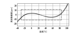
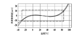
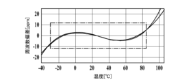
- FIG. 5 is a diagram showing experimental results of temperature characteristics of frequency deviation according to the aspect ratio of excitation electrodes.
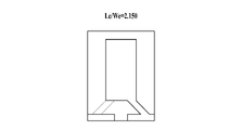
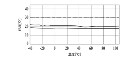
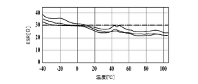
- FIG. 5 is a diagram showing experimental results of temperature characteristics of ESR depending on the aspect ratio of excitation electrodes. It is a figure which shows an example of the aspect ratio of an excitation electrode.
- FIG. 5 is a diagram showing experimental results of temperature characteristics of frequency deviation according to the aspect ratio of excitation electrodes.
- FIG. 5 is a diagram showing experimental results of temperature characteristics of ESR depending on the aspect ratio of excitation electrodes. It is a figure which shows an example of the aspect ratio of an excitation electrode.
- FIG. 5 is a diagram showing experimental results of temperature characteristics of frequency deviation according to the aspect ratio of excitation electrodes.
- FIG. 5 is a diagram showing experimental results of temperature characteristics of ESR depending on the aspect ratio of excitation electrodes. It is a figure which shows an example of the aspect ratio of an excitation electrode.
- FIG. 5 is a diagram showing experimental results of temperature characteristics of frequency deviation according to the aspect ratio of excitation electrodes.
- FIG. 5 is a diagram showing experimental results of temperature characteristics of ESR depending on the aspect ratio of excitation electrodes. It is a figure which shows an example of the aspect ratio of an excitation electrode.
- FIG. 5 is a diagram showing experimental results of temperature characteristics of frequency deviation according to the aspect ratio of excitation electrodes.
- FIG. 5 is a diagram showing experimental results of temperature characteristics of ESR depending on the aspect ratio of excitation electrodes.
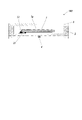
- FIG. 1 is a diagram showing a cross-sectional shape of a crystal device 100 of this embodiment.
- a crystal device 100 includes a crystal resonator element 1, a base 2, a lid 3, a component 4, and the like.
- the substrate 2 is not particularly limited, but is, for example, a ceramic material, a semiconductor material, a glass material, or a combination thereof.
- the base 2 has a concave portion 2a in the center on the upper surface side.
- An electrode pad 21 is positioned on the bottom surface of the recess 2a, and the electrode pad 21 has a planar upper surface and can be formed by, for example, screen printing. Also, the uppermost surface of the electrode pad 21 may be plated with gold.
- the crystal vibrating element 1 is adhered to the electrode pads 21 with a conductive adhesive 22 .
- the conductive adhesive 22 may be, for example, a resin-based (epoxy resin, etc.) adhesive containing silver filler.
- the vibrating (oscillating) portion of the crystal vibrating element 1 is fixed in a floating state without coming into contact with the inner wall surface of the recess 2a.
- the upper surface side of the concave portion of the base 2, that is, the upper end of the frame surrounding the concave portion 2a is joined to the lid 3 via a conductive sealing member such as gold tin or silver solder. Thereby, the recess 2a is sealed.
- a conductive frame-shaped metallized layer may be positioned between the base 2 and the lid 3 .
- the electrode pads 21 can be electrically connected to the outside via a signal line (not shown) passing through the base 2 (for example, external connection pads located on the bottom surface of the base 2 can be connected to external wiring or a substrate).
- a component 4 is positioned on the bottom side of the base 2 .
- the component 4 may be an electronic component such as an IC chip, or may be a sensor such as a temperature detecting element (thermistor, etc.). Also, the component 4 may be a combination of a plurality of these.
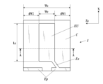
- FIG. 2A is a plan view showing the configuration of the crystal resonator element 1 of this embodiment.
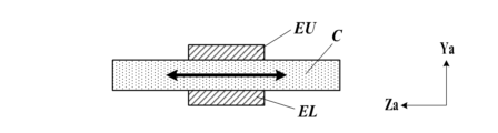
- FIG. 2B is a cross-sectional view taken along section line AA in FIG. 2A.
- FIG. 2C is a side view of the crystal vibrating element 1.
- the crystal vibrating element 1 has a crystal piece C, excitation electrodes EU and EL (electrodes) located on both sides of the crystal piece C, lead lines Ex (lead conductors), and connection electrodes Ep.
- the crystal blank C is obtained by AT cut, and has a thickness corresponding to the range of 74 MHz to 78 MHz so that the oscillation frequency is in the range of 50 MHz to 100 MHz, and in particular, the nominal frequency is 76.8 MHz. It is determined by As shown in FIGS. 2A and 2C, generally, the direction (first direction) along the crystal axis (electrical axis) of quartz is the X-axis. Also, the direction along the optical axis of the crystal is defined as the Z axis, and as shown in FIG. ). The direction intersecting the X-axis and the Za-axis (thickness direction of the crystal piece C) is the Ya-axis direction.
- the X-axis direction is the long-axis direction of the crystal piece C
- the Za-axis direction is the short-axis direction of the crystal piece C. As shown in FIG.
- the excitation electrodes EU and EL are bonded to the upper surface (+Ya side) and lower surface (-Ya side) of the crystal piece C at the same position in plan view.
- the crystal piece C deforms and vibrates according to the voltage applied between the excitation electrodes EU and EL.
- the vibration mode of the crystal blank C here is thickness-shear vibration, and displacement occurs in opposite phases on the upper surface side and the lower surface side in the X-axis direction.
- the excitation electrodes EU and EL are rectangular in plan view and smaller in size than the crystal piece C. As shown in FIG.
- the planar view rectangular shape here is not limited to a complete rectangular shape.
- the corners of the excitation electrodes EU and EL may be slightly slanted or rounded.
- the lead line Ex is a linear wiring that electrically connects between the excitation electrodes EU and EL and the connection electrode Ep.
- the lead lines Ex are located on the upper surface and the lower surface of the crystal piece C, respectively, one for each of the excitation electrodes EU and EL.
- connection electrode Ep is connected to the electrode pad 21 of the substrate 2, and is given a predetermined potential difference from the outside when the crystal vibrating element 1 operates. As a result, the crystal oscillation element 1 resonates, and a clock signal of a predetermined frequency (approximately 76.8 MHz) is obtained from the crystal oscillation circuit to which the crystal oscillation element 1 is connected.
- the excitation electrodes EU and EL are smaller in size than the crystal piece C in plan view.
- the vibration range of the crystal blank C in a plan view is designed to substantially overlap with the range of the excitation electrodes EU and EL.
- ESR electronic series resistance, also known as CI (Crystal Impedance)
- the influence on the crystal piece C is relatively reduced by downsizing the excitation electrodes EU and EL.
- the range of the excitation electrodes EU and EL is made smaller than the vibration range in the X-axis direction, the voltage (power) required to obtain the necessary resonance wave increases, and the power consumption efficiency decreases.
- the lengths of the excitation electrodes EU and EL in the X-axis direction are not significantly changed (a minute design change (for example, several percent) may be allowed).
- Za-axis directions to be smaller than the vibration range thereby suppressing both the influence on the generation of the resonance wave and the influence on the resonance due to the difference in temperature characteristics between the excitation electrodes EU and EL and the crystal blank C. .
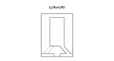
- the ratio of the length in the X-axis direction (vertical length Le) of the excitation electrodes EU and EL to the width in the Za-axis direction (horizontal width We) is 1.993. It is more than 2.525 and less than 2.33.
- the aspect ratio Le/We of the excitation electrodes EU and EL matched to the oscillation range of the crystal blank C is about 1.25, and the crystal vibrating element 1 is significantly longer than this. ing.
- the length Le of the excitation electrodes EU and EL is not much different from the length of the crystal piece C in the vertical direction (X direction), the lengths of the excitation electrodes EU and EL which are smaller than the length of the crystal piece C Increasing the aspect ratio Le/We by increasing the height Le cannot be envisaged here. Moreover, since the aspect ratio Le/We is changed to reduce the size of the excitation electrodes EU and EL, it is not desired to increase the length Le in the first place.
- the width Wc of the crystal blank C is maintained at a conventional size, and the distances dW1 and dW2 between the long sides of the excitation electrodes EU and EL and the long sides of the crystal blank C (from both ends of the crystal blank C extending in the X direction are The respective distances to the excitation electrodes EU and EL) are larger than before.
- the excitation electrodes EU and EL are preferably located near the center position (midpoint) of the crystal piece C in the Za-axis direction.
- the distances dW1 and dW2 are both equal values of 0.130 mm or more and 0.195 mm or less.
- the lead lines Ex are drawn out from the short sides (outer edges extending in the Za direction) of the excitation electrodes EU and EL (one ends are connected to each other) so as to reduce the influence on the vibration of the crystal element C. ), and the other end is connected to the connection electrode Ep.
- the lead line Ex is linear here.
- the influence on the vibration of the crystal piece C can be reduced when the lead line Ex is short.
- the lead line Ex extends at a predetermined angle with respect to the short sides of the excitation electrodes EU and EL, but the inclination angle is not limited to that illustrated. The angle of inclination may be small, and may be perpendicular to the short side, as long as it does not cause problems such as short-circuiting with other conductor portions in manufacturing.
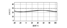
- FIGS. 3A to 3C, FIGS. 4A to 4C, FIGS. 5A to 5C, FIGS. 6A to 6C, and FIGS. 7A to 7C show the case where the excitation electrodes EU and EL have different aspect ratios Le/We (FIG. 3A 7A), the temperature characteristics [ppm] of the frequency deviation (df/f) (FIGS. 3B to 7B) and the temperature characteristics [ ⁇ ] of the ESR (FIGS. 3C to 7C) are obtained experimentally. indicates Here, each ratio Le/We is calculated three times, and each is shown superimposed.
- the crystal resonator element 1 of the present embodiment includes a crystal blank C having an oscillation frequency in the range of 50 MHz to 100 MHz, and planes smaller than the crystal blank C located on both sides of the crystal blank C, respectively.
- rectangular excitation electrodes EU and EL are included in the crystal resonator element 1 of the present embodiment.
- the excitation electrodes EU and EL have a length Le in a first direction along the X-axis (electrical axis) direction of the crystal piece C in a plan view, and a second direction (Za-axis direction) perpendicular to the first direction. ) is 1.993 times or more and 2.525 times or less of the width (horizontal width We).
- we/Le is usually about 1.25, and the excitation electrodes EU and EL are determined so as to substantially match the oscillation range of the crystal blank C.
- the lateral width We is intentionally made shorter than the length Le to set We/Le large, thereby reducing the size of the excitation electrodes EU and EL. While suppressing the level drop, the effect of the difference in the thermal expansion coefficient between the excitation electrodes EU and EL and the crystal blank C is reduced, and the deterioration of the temperature characteristics related to the oscillation of the crystal resonator element 1 is suppressed. It can oscillate stably.
- the oscillation frequency is preferably in the range of 74 MHz or more and 78 MHz or less. That is, the configuration of the present disclosure is preferably used for the crystal vibrating element 1 with a nominal frequency of 76.8 MHz or the like.
- the distance from both ends of the crystal piece C to the ends of the excitation electrodes EU and EL in the second direction (Za-axis direction) in plan view is 0.130 mm or more and 0.195 mm or less. be. That is, since both of the excitation electrodes EU and EL are positioned substantially at the center of the crystal piece C in the Za-axis direction, the portion of the crystal piece C that protrudes (leaks) from the range of the excitation electrodes EU and EL in the Za-axis direction. Since the vibration range is suppressed from reaching both ends of the crystal piece C, the oscillation of the crystal piece C is not hindered, and the crystal oscillation element 1 can be caused to oscillate efficiently.
- the crystal vibrating element 1 also includes a lead line Ex having one end connected to the outer edge (short side) extending along the second direction (Za-axis direction) of the excitation electrodes EU and EL.
- a lead line Ex having one end connected to the outer edge (short side) extending along the second direction (Za-axis direction) of the excitation electrodes EU and EL.
- leader line Ex has a linear shape.
- a shorter lead wire Ex has less influence on the vibration of the crystal element C and can reduce the contamination of external noise, so that the lead wire Ex preferably has a linear shape.
- the crystal device 100 of the present embodiment includes the above-described crystal resonator element 1 . According to this crystal device 100, it is possible to obtain an appropriate signal by oscillating the crystal resonator element 1 with more stable and better temperature characteristics than in the prior art.
- the above-described embodiment is an example, and various modifications are possible.
- the component 4 does not necessarily have to be included. It may be a crystal package that is simply enclosed in a base and a lid, oscillates, and outputs a signal. Further, the crystal vibrating element 1 does not have to be adhered to the substrate 2 as the crystal device 100 .
- the crystal vibrating element 1 may be sold as a single unit.
- the shapes of the base 2 and the lid 3 may be appropriately changed so that the crystal oscillator 1 can be properly housed and sealed, and the signal lines and the electrode pads 21 can be properly positioned. good.
- the shape of the crystal piece C may be finely adjusted in thickness at the ends thereof.
- the crystal element C has been described as having the same thickness (flat shape) in the vibrating portion where the excitation electrodes EU and EL are located and the fixed portion where the connection electrode Ep is located. It may be determined to be larger than the thickness of the vibrating portion (step shape) so that the crystal blank C can be supported more stably.
- the shape of the lead line Ex is not limited to the shape shown in the above embodiment. It may have a bent portion or a curved portion, and may not be pulled out from the short side of the excitation electrodes EU and EL.
- the nominal frequency is 76.8 MHz. Since it is effective, it may be a crystal resonator element 1 that oscillates other frequency signals within the range.
- the specific configurations, structures, materials, and the like shown in the above embodiments can be changed as appropriate without departing from the gist of the present disclosure.
- the scope of the present invention includes the scope described in the claims and their equivalents.
- the present disclosure can be used for crystal oscillators and crystal devices.
Landscapes
- Physics & Mathematics (AREA)
- Acoustics & Sound (AREA)
- Piezo-Electric Or Mechanical Vibrators, Or Delay Or Filter Circuits (AREA)
Priority Applications (3)
| Application Number | Priority Date | Filing Date | Title |
|---|---|---|---|
| US18/682,641 US20240349613A1 (en) | 2021-08-26 | 2022-08-08 | Crystal vibration element and crystal device |
| JP2023543795A JP7645386B2 (ja) | 2021-08-26 | 2022-08-08 | 水晶振動素子及び水晶デバイス |
| CN202280057495.4A CN117837083A (zh) | 2021-08-26 | 2022-08-08 | 晶体振动元件以及晶体器件 |
Applications Claiming Priority (2)
| Application Number | Priority Date | Filing Date | Title |
|---|---|---|---|
| JP2021-137676 | 2021-08-26 | ||
| JP2021137676 | 2021-08-26 |
Publications (1)
| Publication Number | Publication Date |
|---|---|
| WO2023026835A1 true WO2023026835A1 (ja) | 2023-03-02 |
Family
ID=85323101
Family Applications (1)
| Application Number | Title | Priority Date | Filing Date |
|---|---|---|---|
| PCT/JP2022/030212 Ceased WO2023026835A1 (ja) | 2021-08-26 | 2022-08-08 | 水晶振動素子及び水晶デバイス |
Country Status (4)
| Country | Link |
|---|---|
| US (1) | US20240349613A1 (cg-RX-API-DMAC7.html) |
| JP (1) | JP7645386B2 (cg-RX-API-DMAC7.html) |
| CN (1) | CN117837083A (cg-RX-API-DMAC7.html) |
| WO (1) | WO2023026835A1 (cg-RX-API-DMAC7.html) |
Citations (6)
| Publication number | Priority date | Publication date | Assignee | Title |
|---|---|---|---|---|
| JP2014116977A (ja) * | 2014-02-05 | 2014-06-26 | Seiko Epson Corp | 振動片および振動子 |
| JP2014192712A (ja) * | 2013-03-27 | 2014-10-06 | Kyocera Crystal Device Corp | 水晶デバイス |
| JP2017079390A (ja) * | 2015-10-20 | 2017-04-27 | セイコーエプソン株式会社 | 振動素子、発振器、電子機器、移動体および基地局 |
| JP2017152943A (ja) * | 2016-02-25 | 2017-08-31 | 京セラ株式会社 | 水晶振動素子及び水晶振動デバイス |
| JP2018129606A (ja) * | 2017-02-07 | 2018-08-16 | 日本電波工業株式会社 | 水晶振動子及び水晶発振器 |
| JP2020025344A (ja) * | 2019-11-15 | 2020-02-13 | セイコーエプソン株式会社 | 振動素子、振動子、電子デバイス、電子機器、移動体および振動素子の製造方法 |
Family Cites Families (2)
| Publication number | Priority date | Publication date | Assignee | Title |
|---|---|---|---|---|
| JP2001053036A (ja) * | 1999-08-16 | 2001-02-23 | Toyo Commun Equip Co Ltd | ダイシングブレード及び圧電素板 |
| JP3403159B2 (ja) * | 2000-09-22 | 2003-05-06 | 京セラ株式会社 | 圧電発振器 |
-
2022
- 2022-08-08 US US18/682,641 patent/US20240349613A1/en active Pending
- 2022-08-08 CN CN202280057495.4A patent/CN117837083A/zh active Pending
- 2022-08-08 WO PCT/JP2022/030212 patent/WO2023026835A1/ja not_active Ceased
- 2022-08-08 JP JP2023543795A patent/JP7645386B2/ja active Active
Patent Citations (6)
| Publication number | Priority date | Publication date | Assignee | Title |
|---|---|---|---|---|
| JP2014192712A (ja) * | 2013-03-27 | 2014-10-06 | Kyocera Crystal Device Corp | 水晶デバイス |
| JP2014116977A (ja) * | 2014-02-05 | 2014-06-26 | Seiko Epson Corp | 振動片および振動子 |
| JP2017079390A (ja) * | 2015-10-20 | 2017-04-27 | セイコーエプソン株式会社 | 振動素子、発振器、電子機器、移動体および基地局 |
| JP2017152943A (ja) * | 2016-02-25 | 2017-08-31 | 京セラ株式会社 | 水晶振動素子及び水晶振動デバイス |
| JP2018129606A (ja) * | 2017-02-07 | 2018-08-16 | 日本電波工業株式会社 | 水晶振動子及び水晶発振器 |
| JP2020025344A (ja) * | 2019-11-15 | 2020-02-13 | セイコーエプソン株式会社 | 振動素子、振動子、電子デバイス、電子機器、移動体および振動素子の製造方法 |
Also Published As
| Publication number | Publication date |
|---|---|
| US20240349613A1 (en) | 2024-10-17 |
| JP7645386B2 (ja) | 2025-03-13 |
| CN117837083A (zh) | 2024-04-05 |
| JPWO2023026835A1 (cg-RX-API-DMAC7.html) | 2023-03-02 |
Similar Documents
| Publication | Publication Date | Title |
|---|---|---|
| US7061167B2 (en) | Tuning-fork-type piezoelectric vibrating reed and tuning-fork-type piezoelectric vibrator | |
| JP5522796B2 (ja) | 圧電デバイス | |
| US9030078B2 (en) | Vibrating element, vibrator, oscillator, and electronic device | |
| CN103326690B (zh) | 振动片、振子、电子器件以及电子设备 | |
| US7608986B2 (en) | Quartz crystal resonator | |
| CN102111120B (zh) | 弯曲振动片、振动装置以及电子设备 | |
| CN1384601A (zh) | 压电器件 | |
| CN101286729A (zh) | 音叉弯曲晶体振动器件、晶体振动器和晶体振荡器 | |
| JPH08242026A (ja) | 圧電振動子及びこれを具備する圧電振動子デバイス並びに該デバイスを具備する回路装置 | |
| JP2009188483A (ja) | 圧電デバイス及び表面実装型圧電発振器 | |
| JP5668392B2 (ja) | 圧電振動素子、圧電振動子及び圧電発振器 | |
| JP2015186196A (ja) | 圧電振動片及び圧電デバイス | |
| US6525449B1 (en) | Piezoelectric resonator utilizing a harmonic in a thickness-extensional vibration mode | |
| JP7645386B2 (ja) | 水晶振動素子及び水晶デバイス | |
| US12562708B2 (en) | Vibrator device | |
| US20230155568A1 (en) | Vibrator device | |
| JP7632079B2 (ja) | 電子部品用パッケージ、電子部品、及び発振器 | |
| JP4172774B2 (ja) | 表面実装型圧電発振器 | |
| JP5621285B2 (ja) | 振動片、振動子および発振器 | |
| JP4890914B2 (ja) | 水晶振動片の支持部構造 | |
| JP2012119853A (ja) | 圧電デバイス | |
| JP2007180885A (ja) | 圧電デバイス | |
| JP2003224425A (ja) | 温度補償型圧電発振器 | |
| JP5122902B2 (ja) | 圧電発振器 | |
| JP4817929B2 (ja) | 水晶振動片の支持部構造 |
Legal Events
| Date | Code | Title | Description |
|---|---|---|---|
| 121 | Ep: the epo has been informed by wipo that ep was designated in this application |
Ref document number: 22861125 Country of ref document: EP Kind code of ref document: A1 |
|
| WWE | Wipo information: entry into national phase |
Ref document number: 2023543795 Country of ref document: JP |
|
| WWE | Wipo information: entry into national phase |
Ref document number: 18682641 Country of ref document: US |
|
| WWE | Wipo information: entry into national phase |
Ref document number: 202280057495.4 Country of ref document: CN |
|
| NENP | Non-entry into the national phase |
Ref country code: DE |
|
| 122 | Ep: pct application non-entry in european phase |
Ref document number: 22861125 Country of ref document: EP Kind code of ref document: A1 |