WO2023013702A1 - 熱電変換素子 - Google Patents
熱電変換素子 Download PDFInfo
- Publication number
- WO2023013702A1 WO2023013702A1 PCT/JP2022/029861 JP2022029861W WO2023013702A1 WO 2023013702 A1 WO2023013702 A1 WO 2023013702A1 JP 2022029861 W JP2022029861 W JP 2022029861W WO 2023013702 A1 WO2023013702 A1 WO 2023013702A1
- Authority
- WO
- WIPO (PCT)
- Prior art keywords
- thermoelectric conversion
- conversion element
- thermoelectric
- less
- thickness
- Prior art date
- Legal status (The legal status is an assumption and is not a legal conclusion. Google has not performed a legal analysis and makes no representation as to the accuracy of the status listed.)
- Ceased
Links
Images


Classifications
-
- H—ELECTRICITY
- H10—SEMICONDUCTOR DEVICES; ELECTRIC SOLID-STATE DEVICES NOT OTHERWISE PROVIDED FOR
- H10N—ELECTRIC SOLID-STATE DEVICES NOT OTHERWISE PROVIDED FOR
- H10N15/00—Thermoelectric devices without a junction of dissimilar materials; Thermomagnetic devices, e.g. using the Nernst-Ettingshausen effect
-
- H—ELECTRICITY
- H10—SEMICONDUCTOR DEVICES; ELECTRIC SOLID-STATE DEVICES NOT OTHERWISE PROVIDED FOR
- H10N—ELECTRIC SOLID-STATE DEVICES NOT OTHERWISE PROVIDED FOR
- H10N15/00—Thermoelectric devices without a junction of dissimilar materials; Thermomagnetic devices, e.g. using the Nernst-Ettingshausen effect
- H10N15/20—Thermomagnetic devices using thermal change of the magnetic permeability, e.g. working above and below the Curie point
-
- G—PHYSICS
- G01—MEASURING; TESTING
- G01K—MEASURING TEMPERATURE; MEASURING QUANTITY OF HEAT; THERMALLY-SENSITIVE ELEMENTS NOT OTHERWISE PROVIDED FOR
- G01K7/00—Measuring temperature based on the use of electric or magnetic elements directly sensitive to heat ; Power supply therefor, e.g. using thermoelectric elements
- G01K7/02—Measuring temperature based on the use of electric or magnetic elements directly sensitive to heat ; Power supply therefor, e.g. using thermoelectric elements using thermoelectric elements, e.g. thermocouples
-
- H—ELECTRICITY
- H10—SEMICONDUCTOR DEVICES; ELECTRIC SOLID-STATE DEVICES NOT OTHERWISE PROVIDED FOR
- H10N—ELECTRIC SOLID-STATE DEVICES NOT OTHERWISE PROVIDED FOR
- H10N19/00—Integrated devices, or assemblies of multiple devices, comprising at least one thermoelectric or thermomagnetic element covered by groups H10N10/00 - H10N15/00
Definitions
- the present invention relates to thermoelectric conversion elements.
- thermoelectric conversion elements for heat-related measurements.
- Patent Document 1 describes a heat flux sensor module that measures the in-plane distribution of heat flux.
- a heat flux sensor module a plurality of sensor chips having thermoelectric members that generate thermoelectromotive force by the Seebeck effect are arranged on one surface of a base film.
- a heat conducting member is arranged between adjacent sensor chips. The thermal conductivity of this thermally conductive member is higher than that of air.
- Patent Document 2 describes a thermoelectric power generation device that utilizes the anomalous Nernst effect.
- the anomalous Nernst effect is a phenomenon in which a voltage is generated in a direction orthogonal to both the magnetization direction and the temperature gradient when a heat flow is applied to a magnetic material and a temperature difference is generated.
- a plurality of thin wires, which are power generation bodies, are formed along the surface of a substrate whose surface layer is at least made of MgO.
- thermoelectric conversion elements for heat sensing.
- the heat flux sensor module described in Patent Document 1 uses a thermoelectric member that generates a thermoelectromotive force by the Seebeck effect. In this case, it is considered that a large thickness of the thermoelectric member is advantageous for increasing the sensing sensitivity. Therefore, in the heat flux sensor module described in Patent Document 1, it is difficult to reduce the thickness of the sensor chip. For this reason, it is difficult to reduce the thermal resistance of the sensor chip, and it is assumed that the thermal resistance of the sensor chip will affect the heat absorption and heat release characteristics of the measurement target, making it difficult to accurately grasp the true state of the measurement target. be done. In addition, it is considered that heat is less likely to be released due to the thermal resistance of the sensor chip. Therefore, if the thermal resistance of the thermoelectric conversion element can be reduced, the value of the thermoelectric conversion element will increase from the viewpoint of heat sensing.
- thermoelectric power generation device described in Patent Document 2 utilizes the anomalous Nernst effect, the thermal resistance of the thermoelectric power generation device has not been specifically studied.
- the heat flux sensor module described in Patent Document 1 uses a thermoelectric member that generates thermoelectromotive force by the Seebeck effect, and it is considered that the heat flux sensor module has relatively high flexural rigidity. Therefore, it is understood that it is difficult to arrange this heat flux sensor module along the curved surface. Moreover, even if the heat flux sensor module can be arranged along the curved surface, there is a high possibility that air bubbles will form at the adhesion point between the heat flux sensor module and the curved surface due to its high flexural rigidity. The presence of such bubbles can greatly affect the heat absorption and heat dissipation characteristics, and can cause problems in the reliability of heat flux measurement results. On the other hand, if the thermoelectric conversion element can be arranged along the curved surface, thermal resistance is less likely to occur between the thermoelectric conversion element and the object to be measured, and the value of the thermoelectric conversion element is considered to increase from the viewpoint of heat sensing.
- thermoelectric power generation device described in Patent Document 2 utilizes the anomalous Nernst effect, the bending rigidity of the thermoelectric power generation device has not been specifically studied.
- thermoelectric conversion element that is advantageous from the viewpoint of reducing thermal resistance.
- thermoelectric conversion element a substrate; and a thermoelectric converter arranged on the base material
- the thermoelectric conversion element satisfies both the following condition (I), the following condition (II), or the following conditions (I) and (II):
- a thermoelectric conversion element is provided.
- the value obtained by dividing the thickness of the thermoelectric conversion element in the thickness direction of the substrate by the thermal conductivity of the thermoelectric conversion element in the thickness direction of the substrate is 9 ⁇ 10 ⁇ 4 m 2 KW ⁇ 1 or less.
- a value obtained by dividing the flexural rigidity of the thermoelectric conversion element by the width of the thermoelectric conversion element is 3 ⁇ 10 ⁇ 6 Pa ⁇ m 4 /mm or less.
- thermoelectric conversion element is advantageous from the viewpoint of reducing thermal resistance.
- FIG. 1 is a perspective view showing one example of a thermoelectric conversion element according to the present invention.
- FIG. 2 is a cross-sectional view of the thermoelectric conversion element taken along plane II shown in FIG.
- FIG. 3 is a diagram schematically showing a method of evaluating flexibility of a thermoelectric conversion element.
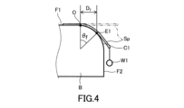
- FIG. 4 is a diagram schematically showing a method of evaluating flexibility of a thermoelectric conversion element.
- the thermoelectric conversion element 1a includes a substrate 10 and a thermoelectric conversion body 21. As shown in FIG. A thermoelectric converter 21 is arranged on the substrate 10 . As shown in FIG. 2, the thermoelectric conversion element 1a has dimensions represented by a thickness td and a width Wd .
- the thermoelectric conversion element 1a satisfies the following condition (I), the following condition (II), or both the following conditions (I) and (II). In other words, the thermoelectric conversion element 1a may satisfy only the following condition (I), may satisfy only the following condition (II), or may satisfy the following conditions (I) and (II). Both may be satisfied.
- thermoelectric conversion element 1a The value td / ⁇ d obtained by dividing the thickness td of the thermoelectric conversion element 1a in the thickness direction of the substrate 10 by the thermal conductivity ⁇ d of the thermoelectric conversion element 1a in the thickness direction of the substrate 10 is 9 ⁇ 10 ⁇ 4 m 2 KW ⁇ 1 or less.
- a value EI/ Wd obtained by dividing the flexural rigidity EI of the thermoelectric conversion element 1a by the width Wd of the thermoelectric conversion element 1a is 3 ⁇ 10 ⁇ 6 Pa ⁇ m 4 /mm or less.
- thermoelectric conversion element 1a When the thermoelectric conversion element 1a satisfies the above condition (I), the thermal resistance of the thermoelectric conversion element 1a itself in the thickness direction of the substrate 10 tends to be low. For this reason, for example, when the thermoelectric conversion element 1a is used for heat sensing, the thermoelectric conversion element 1a is less likely to affect the heat absorption and heat release characteristics in the vicinity of the measurement object, and captures a state close to the true state of the measurement object. be able to.
- the thermoelectric conversion element 1a may be used for applications other than heat sensing, and may be used as a power source, for example.
- thermoelectric conversion element 1a is a value at 25° C., for example.
- the thermal conductivity ⁇ d can be determined by the method described in the Examples, for example according to the laser flash method.
- thermoelectric conversion element 1a may desirably satisfy the condition of t d / ⁇ d ⁇ 9 ⁇ 10 -4 m 2 KW -1 in the temperature range of -50°C to 180°C.
- t d / ⁇ d may be 8 ⁇ 10 ⁇ 4 m 2 KW ⁇ 1 or less, 7 ⁇ 10 ⁇ 4 m 2 KW ⁇ 1 or less, or 6 ⁇ 10 ⁇ 4 m 2 KW ⁇ It may be 1 or less, 5 ⁇ 10 ⁇ 4 m 2 KW ⁇ 1 or less, or 4 ⁇ 10 ⁇ 4 m 2 KW ⁇ 1 or less.
- t d / ⁇ d is, for example, 8 ⁇ 10 ⁇ 7 m 2 KW ⁇ 1 or more. This is desirable from the viewpoint of handleability of the thermoelectric conversion element 1a.
- thermoelectric conversion element 1a When the thermoelectric conversion element 1a satisfies the condition (II) above, it is easy to arrange the thermoelectric conversion element 1a along the curved surface, and it is difficult to form an air layer or bubbles between the curved surface and the thermoelectric conversion element 1a.
- a thermoelectric conversion element When a thermoelectric conversion element is used for heat sensing, the existence of an air layer or air bubbles between the thermoelectric conversion element and the object to be measured greatly affects the heat absorption and radiation characteristics in the vicinity of the object to be measured.
- the thermoelectric conversion element 1a satisfies the above condition (II), it is difficult to form an air layer or bubbles when the thermoelectric conversion element 1a is arranged along the curved surface.
- thermoelectric conversion element 1a is attached along the curved surface, the thermoelectric conversion element 1a is less likely to come off.
- the flexural rigidity of the thermoelectric conversion element 1a is obtained, for example, by performing a tensile test on a test piece prepared from the thermoelectric conversion element 1a, measuring the Young's modulus E (tensile elastic modulus) of the thermoelectric conversion element 1a, and determining the Young's modulus E and the geometrical moment of inertia I.
- the Young's modulus E of the thermoelectric conversion element 1a is, for example, a tensile elastic modulus when a tensile stress is applied in the Y-axis direction to a test piece produced from the thermoelectric conversion element 1a.
- the flexural rigidity EI of the thermoelectric conversion element 1a is measured by fixing a rectangular test piece made from the thermoelectric conversion element 1a in a cantilevered state, attaching a predetermined weight to the tip of the test piece, and bending and deforming the test piece. may be determined by
- EI/W d may be 2.5 ⁇ 10 ⁇ 6 Pa ⁇ m 4 /mm or less, or may be 2 ⁇ 10 ⁇ 6 Pa ⁇ m 4 /mm or less, It may be 1 ⁇ 10 ⁇ 6 Pa ⁇ m 4 /mm or less, 7 ⁇ 10 ⁇ 7 Pa ⁇ m 4 /mm or less, or 5 ⁇ 10 ⁇ 7 Pa ⁇ m 4 /mm or less.
- EI/W d is, for example, 3 ⁇ 10 ⁇ 11 Pa ⁇ m 4 /mm or more. Thereby, the thermoelectric conversion element 1a tends to have desired handleability.
- thermoelectric conversion element 1a As long as the thermoelectric conversion element 1a satisfies the condition (I), the condition (II), or both the conditions (I) and (II), the thermoelectric effect exhibited by the thermoelectric conversion body 21 is limited to a specific thermoelectric effect. not.
- the thermoelectric converter 21 generates an electromotive force in a direction orthogonal to the thickness direction of the base 10 when a temperature gradient ⁇ T is generated in the thickness direction (Z-axis direction) of the base 10, for example. Accordingly, for example, in order to increase the power generated by the temperature gradient in the thermoelectric conversion element 1a, it is not necessary to adjust the thickness of the thermoelectric conversion element 1a to a large extent, unlike the thermoelectric conversion element utilizing the Seebeck effect.
- thermoelectric converter 21 by increasing the dimension of the thermoelectric converter 21 in a specific direction along the main surface of the base material 10, the electric power generated by the temperature gradient ⁇ T in the thermoelectric conversion element 1a can be increased. Therefore, it is easy to reduce the thickness of the thermoelectric conversion element 1a, and it is easy to adjust t d / ⁇ d to a desired range or EI/W d to a desired range.
- the thermoelectric converter 21 generates an electromotive force by, for example, a magneto-thermoelectric effect.
- the magneto-thermoelectric effect is, for example, the anomalous Nernst effect or the spin Seebeck effect.
- the thermoelectric converter 21 contains, for example, a material exhibiting the anomalous Nernst effect. Substances exhibiting the anomalous Nernst effect are not limited to specific substances. A material exhibiting the anomalous Nernst effect is, for example, a magnetic material having a saturation magnetic susceptibility of 5 ⁇ 10 ⁇ 3 T or more or a material having a band structure having a Weyl point near the Fermi energy.
- the thermoelectric converter 21 contains at least one substance selected from the group consisting of the following (i), (ii), (iii), (iv), and (v) as a substance exhibiting an anomalous Nernst effect. do.
- a stoichiometric substance having a composition represented by Fe 3 X (ii) an off-stoichiometric substance in which the composition ratio of Fe and X deviates from the substance (i) above (iii) the above ( A substance (iv) Fe 3 M1 1-x M2 x (iv) in which a part of the Fe site of the substance i) or part of the Fe site of the substance (ii) is replaced with a typical metal element other than X or a transition element (v) a substance having a composition represented by 0 ⁇ x ⁇ 1), wherein M1 and M2 are different representative elements; , a substance in which a part of the X site of the substance (i) above is replaced with a main group metal element other than X
- X is a typical element or a transition element.
- X is, for example, Al, Ga, Ge, Sn, Si, Ti, Zr, Hf, V, Nb, Ta, Cr, Mo, W, Sc, Ni, Mn, or Co.
- the combination of M1 and M2 is not limited to a specific combination as long as M1 and M2 are representative elements different from each other.
- the combination of M1 and M2 is Ga and Al, Si and Al, or Ga and B, for example.
- the thermoelectric converter 21 may contain Co 2 MnGa or Mn 3 Sn as the substance exhibiting the anomalous Nernst effect.
- the thermoelectric conversion body 21 is formed, for example, in a rectangular parallelepiped shape elongated in a specific direction (Y-axis direction) extending along the main surface of the substrate 10 .
- the thermoelectric converter 21 is magnetized, for example, in the negative direction of the X-axis.
- a temperature gradient is generated in the thickness direction of the base material 10 and a heat flow is generated in the positive Z-axis direction
- an electromotive force is generated in the positive Y-axis direction orthogonal to the Z-axis and the X-axis according to the magneto-thermoelectric effect.
- the dimension of the thermoelectric converter 21 in the Y-axis direction is larger than the dimensions of the thermoelectric converter 21 in the Z-axis and the X-axis, and the electromotive force generated by the magneto-thermoelectric effect tends to be large. Therefore, even if the thermoelectric conversion body 21 does not have a large thickness, the electromotive force generated in the thermoelectric conversion element 1a tends to increase.
- the thermoelectric conversion element 1a includes, for example, conductive paths 25.
- Conductive path 25 includes thermoelectric converter 21 and forms a meander pattern.
- the length of the conductive path 25 tends to increase, and the electromotive force generated in the thermoelectric conversion element 1a tends to increase.
- the electromotive force generated in the thermoelectric conversion element 1a can be extracted to the outside.
- the conductive path 25 includes a plurality of thermoelectric converters 21.
- the plurality of thermoelectric conversion bodies 21 are, for example, separated at predetermined intervals in the X-axis direction and arranged parallel to each other.
- the thermoelectric converters 21 are arranged at regular intervals in the X-axis direction.
- Conductive path 25 further comprises, for example, a plurality of connectors 22 .
- the connection bodies 22 electrically connect the thermoelectric conversion bodies 21 adjacent to each other in the X-axis direction.
- the connector 22 electrically connects, for example, one end of the thermoelectric conversion body 21 in the Y-axis direction and the other end in the Y-axis direction of another thermoelectric conversion body 21 adjacent to the thermoelectric conversion body 21 .
- the plurality of thermoelectric converters 21 are electrically connected in series, and the electromotive force generated in the thermoelectric conversion element 1a tends to increase.
- One end of the plurality of thermoelectric conversion bodies 21 in the Y-axis direction is located at the end of the same side of the thermoelectric conversion bodies 21 in the Y-axis direction, and the other end of the plurality of thermoelectric conversion bodies 21 in the Y-axis direction is located at , are located at the end of the thermoelectric converter 21 opposite to the one end in the Y-axis direction.
- connection body 22 is formed, for example, in the shape of a rectangular parallelepiped elongated in the Y-axis direction.
- the connecting body 22 can electrically connect the adjacent thermoelectric conversion bodies 21, the material forming the connecting body 22 is not limited to a specific material.
- the connector 22 may contain a substance that generates an electromotive force by a magneto-thermoelectric effect, and may have ferromagnetism or antiferromagnetism, for example. In this case, the connector 22 is magnetized, for example, in the positive direction of the X-axis.
- the connector 22 may contain a non-magnetic material.
- the material forming the connector 22 is, for example, a transition element having paramagnetism.
- the non-magnetic material contained in the connector 22 is, for example, gold, copper, copper alloy, aluminum, or aluminum alloy.
- the connector 22 may be a cured conductive paste.
- the thickness of the thermoelectric conversion element 1a is not limited to a specific value.
- the thickness of the thermoelectric conversion element 1a is, for example, 200 ⁇ m or less. As a result, the thermal resistance of the thermoelectric conversion element 1a in the thickness direction of the substrate 10 tends to be low, or EI/ Wd can be easily adjusted within a desired range.
- the thickness of the thermoelectric conversion element 1a may be 190 ⁇ m or less, 180 ⁇ m or less, 170 ⁇ m or less, or 160 ⁇ m or less.
- the thickness of the thermoelectric conversion element 1a is desirably 150 ⁇ m or less.
- the thickness of the thermoelectric conversion element 1a may be 140 ⁇ m or less, 130 ⁇ m or less, 120 ⁇ m or less, 110 ⁇ m or less, or 100 ⁇ m or less. good.
- the thickness of the thermoelectric conversion element 1a may be 90 ⁇ m or less, 80 ⁇ m or less, 70 ⁇ m or less, or 60 ⁇ m or less.
- the thickness of the thermoelectric conversion element 1a is, for example, 10 ⁇ m or more. Thereby, the thermoelectric conversion element 1a tends to have desired handleability.
- the thickness of the thermoelectric conversion element 1a may be 20 ⁇ m or more, or may be 30 ⁇ m or more.
- the material forming the base material 10 is not limited to a specific material.
- the base material 10 does not contain MgO in the surface layer, for example. As a result, it is not necessary to include MgO in the surface layer of the base material 10, so the production of the thermoelectric conversion element 1a is less complicated.
- the base material 10 has flexibility, for example. Thereby, the thermoelectric conversion elements 1a can be arranged along the curved surface.
- the base material 10 is, for example, a strip-shaped test piece made from the base material 10. When the test piece is wound around a cylindrical mandrel with a diameter of 10 cm so that both ends of the test piece in the length direction are oriented in the same direction, the The test piece has elasticity that allows it to be elastically deformed.
- the base material 10 may be a non-flexible material such as a glass base material.
- the substrate 10 When the substrate 10 has flexibility, the substrate 10 contains at least an organic polymer, for example. Thereby, it is easy to reduce the manufacturing cost of the thermoelectric conversion element 1a.
- organic polymers are polyethylene terephthalate (PET), polyethylene naphthalate (PEN), acrylic resin (PMMA), polycarbonate (PC), polyimide (PI) or cycloolefin polymer (COP).
- Substrate 10 may be ultra-thin glass.
- An example of ultra-thin glass is G-Leaf (registered trademark) manufactured by Nippon Electric Glass Co., Ltd.
- the visible light transmittance of the base material 10 is not limited to a specific value.
- the substrate 10 has, for example, a visible light transmittance of 80% or more. As a result, it is easy to confirm the presence or absence of foreign matter in manufacturing the thermoelectric conversion element 1a, and it is possible to suppress the opening of the wiring of the thermoelectric conversion element 1a.
- the visible light transmittance of the substrate 10 may be 83% or more, 86% or more, or 89% or more.
- the thickness of the thermoelectric conversion body 21 is not limited to a specific value.
- the thickness of the thermoelectric converter 21 is, for example, 1000 nm or less.
- the thickness of the thermoelectric converter 21 may be 750 nm or less, 500 nm or less, 400 nm or less, 300 nm or less, or 200 nm or less.
- the thickness of the thermoelectric converter 21 is, for example, 5 nm or more. This makes it easy for the thermoelectric conversion element 1a to exhibit high durability.
- the thickness of the thermoelectric converter 21 may be 10 nm or more, 20 nm or more, 30 nm or more, or 50 nm or more.
- each thermoelectric conversion body 21 As long as the thermoelectric conversion element 1a satisfies the condition (I), the condition (II), or both the conditions (I) and (II), the width, which is the dimension in the X-axis direction, of each thermoelectric conversion body 21 can be specified is not limited to the value of The width of each thermoelectric converter 21 is, for example, 500 ⁇ m or less. As a result, the amount of material used for forming the thermoelectric converters 21 in the thermoelectric conversion element 1a can be reduced, and the manufacturing cost of the thermoelectric conversion element 1a can be easily reduced. In addition, a large number of thermoelectric converters 21 are easily arranged in the X-axis direction, and the electromotive force generated in the thermoelectric conversion element 1a is likely to increase.
- the width of each thermoelectric converter 21 may be 400 ⁇ m or less, 300 ⁇ m or less, or 200 ⁇ m or less.
- the width of each thermoelectric converter 21 is, for example, 0.1 ⁇ m or more. As a result, disconnection of the conductive path 25 is less likely to occur in the thermoelectric conversion element 1a, and the thermoelectric conversion element 1a tends to exhibit high durability.
- the width of each thermoelectric converter 21 may be 0.5 ⁇ m or more, 1 ⁇ m or more, 2 ⁇ m or more, 5 ⁇ m or more, or 10 ⁇ m or more. , 20 ⁇ m or more, or 50 ⁇ m or more.
- the thickness of the connecting body 22 is not limited to a specific value as long as the connecting body 22 can electrically connect the adjacent thermoelectric conversion bodies 21 .
- the thickness of the connector 22 is, for example, 1000 nm or less. This makes it possible to reduce the amount of material used for forming the connection body 22, and it is easy to reduce the manufacturing cost of the thermoelectric conversion element 1a. In addition, disconnection of the conductive path 25 is less likely to occur in the thermoelectric conversion element 1a.
- the thickness of the connector 22 may be 500 nm or less, 400 nm or less, 300 nm or less, or 200 nm or less.
- the thickness of the connector 22 is, for example, 5 nm or more. This makes it easy for the thermoelectric conversion element 1a to exhibit high durability.
- the thickness of the connector 22 may be 10 nm or more, 20 nm or more, 30 nm or more, or 50 nm or more.
- the width which is the minimum dimension of each connecting body 22 in the X-axis direction, is not limited to a specific value.
- the width of each connector 22 is, for example, 500 ⁇ m or less.
- the width of each connector 22 may be 400 ⁇ m or less, 300 ⁇ m or less, 200 ⁇ m or less, 100 ⁇ m or less, or 50 ⁇ m or less.
- the width of each connector 22 is, for example, 0.1 ⁇ m or more. As a result, disconnection of the conductive path 25 is less likely to occur in the thermoelectric conversion element 1a, and the thermoelectric conversion element 1a tends to exhibit high durability.
- the width of each connector 22 may be 0.5 ⁇ m or more, 1 ⁇ m or more, 2 ⁇ m or more, 5 ⁇ m or more, or 10 ⁇ m or more. It may be 20 ⁇ m or more, or may be 30 ⁇ m or more.
- thermoelectric conversion element 1a An example of a method for manufacturing the thermoelectric conversion element 1a will be described.
- a thin film of a precursor of the thermoelectric converter 21 is applied to one main surface of the substrate 10 by methods such as sputtering, chemical vapor deposition (CVD), pulsed laser deposition (PLD), ion plating, and plating.
- CVD chemical vapor deposition
- PLD pulsed laser deposition
- ion plating ion plating
- plating plating.
- a photoresist is then applied over the thin film, a photomask is placed over the thin film and exposed to light, followed by a wet etch. Thereby, a linear pattern of precursors of a plurality of thermoelectric converters 21 arranged at predetermined intervals is formed.
- thermoelectric conversion body 21 is formed by magnetizing the precursor of the thermoelectric conversion body 21 .
- the connector 22 may be formed by magnetizing the precursor of the connector 22 .
- the thermoelectric conversion element 1a may be provided with, for example, an adhesive layer.
- the base material 10 is arranged between the thermoelectric converters 21 and the adhesive layer in the thickness direction of the base material 10 .
- the thermoelectric conversion element 1a can be attached to the article by pressing the adhesive layer against the article.
- the adhesive layer contains, for example, a rubber-based adhesive, an acrylic adhesive, a silicone-based adhesive, or a urethane-based adhesive.
- Thermoelectric conversion element 1a may be provided together with an adhesive layer and a separator.
- the separator covers the adhesive layer.
- a separator is typically a film that can maintain the adhesive strength of the adhesive layer when covering the adhesive layer and that can be easily peeled off from the adhesive layer.
- the separator is, for example, a film made of polyester resin such as PET. By peeling off the separator, the adhesive layer is exposed, and the thermoelectric conversion element 1a can be attached to an article.
- thermoelectric conversion element according to each example and each comparative example was measured.
- thermal conductivity in the thickness direction of the thermoelectric conversion elements according to each example and each comparative example at 25° C. was measured according to the laser flash method using a measuring device LFA467 manufactured by Netsch Japan.
- the thickness of the element according to each example and each comparative example is divided by the thermal conductivity in the thickness direction of the thermoelectric conversion element according to each example and each comparative example.
- a value Rr for the thermal resistance of the conversion element was determined. Table 1 shows the results.
- a test piece for a tensile test was produced from the thermoelectric conversion element according to each example and each comparative example.
- a tensile test was performed on each test piece using a desktop stretching machine manufactured by Linkcom Co., Ltd. to determine the Young's modulus E of each thermoelectric conversion element.
- a tensile stress was applied to the test piece in the longitudinal direction of the FeGa-containing linear pattern in the meander pattern.
- the flexural rigidity EI of each element was determined from the Young's modulus E and the geometrical moment of inertia I of the thermoelectric conversion element according to each example and each comparative example.
- thermoelectric conversion element By dividing this bending rigidity value by the width of each thermoelectric conversion element, a normalized bending rigidity EI n value was determined for each thermoelectric conversion element.
- the width of the thermoelectric conversion element means the dimension of the thermoelectric conversion element in a direction parallel to the main surface of the substrate and perpendicular to the longitudinal direction of the FeGa-containing linear pattern. Table 1 shows the results.
- thermoelectric conversion element according to each example and each comparative example was placed on a hot plate.
- a thermocouple was placed on the surface of each thermoelectric conversion element and the surface of the hot plate on which no thermoelectric conversion element was arranged, and the temperatures of both surfaces were measured.
- the hot plate was heated to 100°C.
- the difference ⁇ t between the time when the temperature of the surface of the thermoelectric conversion element reached 100° C. and the time when the surface of the hot plate on which the thermoelectric conversion element was not arranged reached 100° C. was measured. Table 1 shows the results.
- a block B having a curved surface C1 with a radius of curvature R1 of 10 mm was prepared.
- the curved surface C1 was formed in a range forming an angle of 90° in the cross section of the block perpendicular to the curved surface C1.
- the surfaces F1 and F2 in contact with the curved surface C1 were flat surfaces.
- a strip-shaped test piece Sp was produced from the thermoelectric conversion element according to each example and each comparative example.
- the test piece Sp was placed on the flat surface F1 in contact with the curved surface C1 of the block B, and the test piece Sp was protruded with a length L1 of 30 mm from the starting point O, which is the boundary between the curved surface C1 and the flat surface F1 of the block B. In this state, the test piece Sp was fixed. As shown in FIG. 4, a weight W1 of 5 g was attached to the tip of the test piece Sp, and the test piece Sp was deformed along the curved surface C1.
- [Flexibility evaluation B] A strip-shaped test piece was produced from the thermoelectric conversion element according to each example and each comparative example. A specimen was wound around a horizontally fixed cylindrical mandrel having a diameter of: The test piece was wrapped around the mandrel so that the FeGa-containing linear pattern in the meander pattern straddled the mandrel. After that, the presence or absence of disconnection of the meander pattern in the test piece was confirmed. It was judged that the disconnection of the meander pattern occurred when the electrical resistance value of the meander pattern became 1.5 times or more of the initial value.
- mandrels to be used were selected in descending order of mandrel diameter, and the maximum value of the mandrel diameter at which disconnection of the meander pattern occurred was determined. Table 1 shows the results. (mandrel diameter) 20mm, 18.5mm, 17mm, 15.5mm, 14mm, 12.5mm, 11mm, 9.5mm, 8mm, 6.5mm, 5mm
- Example 1 A thin film having a thickness of 100 nm was formed on a polyethylene terephthalate (PET) film having a thickness of 50 ⁇ m by DC magnetron sputtering using a target material containing Fe and Ga.
- the visible light transmittance of the PET film was 80% or more.
- a photoresist was applied on the thin film, a photomask was placed on the thin film, exposure was performed, and then wet etching was performed. As a result, a plurality of FeGa-containing linear patterns arranged parallel to each other at predetermined intervals were formed. The width of each FeGa-containing linear pattern was 100 ⁇ m.
- a Cu thin film having a thickness of 100 nm was formed by DC magnetron sputtering using a target material containing Cu.
- a photoresist was applied on the Cu thin film, a photomask was placed on the Cu thin film, exposure was performed, and then wet etching was performed.
- a Cu-containing linear pattern having a width of 40 ⁇ m was thereby formed.
- a pair of adjacent FeGa-containing linear patterns were electrically connected to each other by the Cu-containing linear pattern, forming a conductive path forming a meander pattern.
- thermoelectric conversion element generated an electromotive force based on the anomalous Nernst effect.
- thermoelectric conversion element according to Example 2 was produced in the same manner as in Example 1, except that a PET film having a thickness of 100 ⁇ m was used instead of the PET film having a thickness of 50 ⁇ m.
- the visible light transmittance of this PET film was 80% or more.
- thermoelectric conversion element according to Example 3 was produced in the same manner as in Example 1, except that a PET film having a thickness of 125 ⁇ m was used instead of the PET film having a thickness of 50 ⁇ m.
- the visible light transmittance of this PET film was 80% or more.
- thermoelectric conversion element according to Example 4 was produced in the same manner as in Example 1, except that a PET film having a thickness of 188 ⁇ m was used instead of the PET film having a thickness of 50 ⁇ m.
- the visible light transmittance of this PET film was 80% or more.
- thermoelectric conversion element according to Comparative Example 1 was produced in the same manner as in Example 1, except that a PET film having a thickness of 250 ⁇ m was used instead of the PET film having a thickness of 50 ⁇ m.
- thermoelectric conversion element Energy Eye manufactured by Denso Corporation was prepared as a thermoelectric conversion element according to Comparative Example 2. This thermoelectric conversion element generated an electromotive force based on the Seebeck effect. This thermoelectric conversion element used polyimide (PI) as a base material.
- PI polyimide
- the thermal resistance value Rr of the thermoelectric conversion element according to each example is 9 ⁇ 10 ⁇ 4 m 2 KW ⁇ 1 or less, which is higher than the thermal resistance value Rr of the thermoelectric conversion element according to the comparative example. was low. Therefore, it was suggested that the thermoelectric conversion element according to each example is advantageous from the viewpoint of reduction in thermal resistance. In addition, ⁇ t in the thermoelectric conversion element according to each example is shorter than ⁇ t in the thermoelectric conversion element according to the comparative example, suggesting that the thermoelectric conversion element according to each example has advantageous characteristics from the viewpoint of heat sensing. was done.
- thermoelectric conversion element according to each example As shown in Table 1, the standardized flexural rigidity EI n value for the thermoelectric conversion elements according to each example is 3 ⁇ 10 ⁇ 6 Pa ⁇ m 4 /mm or less, and the thermoelectric conversion elements according to the comparative examples have , was smaller than the value of the standardized bending stiffness EI n . Therefore, it was suggested that the thermoelectric conversion element according to each example can be easily deformed and arranged along the curved surface. In addition, the results of flexibility evaluation suggested that the thermoelectric conversion element according to each example had desired flexibility.
- a first aspect of the present invention is A thermoelectric conversion element, a substrate; and a thermoelectric converter arranged on the base material, The thermoelectric conversion element satisfies both the following condition (I), the following condition (II), or the following conditions (I) and (II):
- a thermoelectric conversion element is provided.
- the value obtained by dividing the thickness of the thermoelectric conversion element in the thickness direction of the substrate by the thermal conductivity of the thermoelectric conversion element in the thickness direction of the substrate is 9 ⁇ 10 ⁇ 4 m 2 KW ⁇ 1 or less.
- a value obtained by dividing the flexural rigidity of the thermoelectric conversion element by the width of the thermoelectric conversion element is 3 ⁇ 10 ⁇ 6 Pa ⁇ m 4 /mm or less.
- thermoelectric conversion element according to the first aspect, A thermoelectric conversion element having a thickness of 200 ⁇ m or less is provided.
- thermoelectric conversion element according to the second aspect is provided.
- a fourth aspect of the present invention is the thermoelectric conversion element according to any one of the first to third aspects,
- the substrate provides a thermoelectric conversion element containing no MgO in the surface layer.
- a fifth aspect of the present invention is the thermoelectric conversion element according to any one of the first to fourth aspects,
- the substrate provides a thermoelectric conversion element having flexibility.
- thermoelectric conversion element is the thermoelectric conversion element according to the fifth aspect,
- the substrate provides a thermoelectric conversion element containing at least an organic polymer.
- a seventh aspect of the present invention is the thermoelectric conversion element according to any one of the first to sixth aspects,
- the substrate provides a thermoelectric conversion element having a visible light transmittance of 80% or more.
- thermoelectric conversion body provides a thermoelectric conversion element that generates an electromotive force in a direction perpendicular to the thickness direction of the substrate when a temperature gradient occurs in the thickness direction of the substrate.
- thermoelectric conversion element is the thermoelectric conversion element according to any one of the first to eighth aspects,
- the thermoelectric converter provides a thermoelectric conversion element that generates an electromotive force by a magneto-thermoelectric effect.
- thermoelectric conversion element is the thermoelectric conversion element according to any one of the first to ninth aspects,
- the magnetic material provides a thermoelectric conversion element that generates an electromotive force due to the anomalous Nernst effect.
- thermoelectric conversion element is the thermoelectric conversion element according to any one of the first to tenth aspects, A thermoelectric conversion element is provided, which includes the magnetic material and includes a conductive path forming a meander pattern.
Landscapes
- Physics & Mathematics (AREA)
- General Physics & Mathematics (AREA)
- Measuring Temperature Or Quantity Of Heat (AREA)
Priority Applications (5)
| Application Number | Priority Date | Filing Date | Title |
|---|---|---|---|
| EP22853120.8A EP4383992A4 (en) | 2021-08-06 | 2022-08-03 | THERMOELECTRIC CONVERSION ELEMENT |
| KR1020247007341A KR20240038097A (ko) | 2021-08-06 | 2022-08-03 | 열전 변환 소자 |
| CN202280055090.7A CN117813944A (zh) | 2021-08-06 | 2022-08-03 | 热电转换元件 |
| JP2023540398A JPWO2023013702A1 (https=) | 2021-08-06 | 2022-08-03 | |
| US18/681,670 US20240341193A1 (en) | 2021-08-06 | 2022-08-03 | Thermoelectric conversion element |
Applications Claiming Priority (2)
| Application Number | Priority Date | Filing Date | Title |
|---|---|---|---|
| JP2021-130338 | 2021-08-06 | ||
| JP2021130338 | 2021-08-06 |
Publications (1)
| Publication Number | Publication Date |
|---|---|
| WO2023013702A1 true WO2023013702A1 (ja) | 2023-02-09 |
Family
ID=85156035
Family Applications (1)
| Application Number | Title | Priority Date | Filing Date |
|---|---|---|---|
| PCT/JP2022/029861 Ceased WO2023013702A1 (ja) | 2021-08-06 | 2022-08-03 | 熱電変換素子 |
Country Status (6)
| Country | Link |
|---|---|
| US (1) | US20240341193A1 (https=) |
| EP (1) | EP4383992A4 (https=) |
| JP (1) | JPWO2023013702A1 (https=) |
| KR (1) | KR20240038097A (https=) |
| CN (1) | CN117813944A (https=) |
| WO (1) | WO2023013702A1 (https=) |
Citations (3)
| Publication number | Priority date | Publication date | Assignee | Title |
|---|---|---|---|---|
| JP2014072256A (ja) | 2012-09-28 | 2014-04-21 | Tohoku Univ | 熱電発電デバイス |
| JP2018004475A (ja) | 2016-07-04 | 2018-01-11 | 株式会社デンソー | 熱流束センサモジュールおよびその製造方法 |
| WO2020218613A1 (ja) * | 2019-04-26 | 2020-10-29 | 国立大学法人東京大学 | 熱電変換素子及び熱電変換装置 |
Family Cites Families (2)
| Publication number | Priority date | Publication date | Assignee | Title |
|---|---|---|---|---|
| CN110494997A (zh) * | 2017-03-30 | 2019-11-22 | 琳得科株式会社 | 热电转换模块及其制造方法 |
| WO2019009308A1 (ja) * | 2017-07-03 | 2019-01-10 | 国立大学法人東京大学 | 熱電変換素子及び熱電変換デバイス |
-
2022
- 2022-08-03 WO PCT/JP2022/029861 patent/WO2023013702A1/ja not_active Ceased
- 2022-08-03 CN CN202280055090.7A patent/CN117813944A/zh active Pending
- 2022-08-03 KR KR1020247007341A patent/KR20240038097A/ko active Pending
- 2022-08-03 EP EP22853120.8A patent/EP4383992A4/en active Pending
- 2022-08-03 JP JP2023540398A patent/JPWO2023013702A1/ja active Pending
- 2022-08-03 US US18/681,670 patent/US20240341193A1/en active Pending
Patent Citations (3)
| Publication number | Priority date | Publication date | Assignee | Title |
|---|---|---|---|---|
| JP2014072256A (ja) | 2012-09-28 | 2014-04-21 | Tohoku Univ | 熱電発電デバイス |
| JP2018004475A (ja) | 2016-07-04 | 2018-01-11 | 株式会社デンソー | 熱流束センサモジュールおよびその製造方法 |
| WO2020218613A1 (ja) * | 2019-04-26 | 2020-10-29 | 国立大学法人東京大学 | 熱電変換素子及び熱電変換装置 |
Non-Patent Citations (1)
| Title |
|---|
| See also references of EP4383992A4 |
Also Published As
| Publication number | Publication date |
|---|---|
| JPWO2023013702A1 (https=) | 2023-02-09 |
| CN117813944A (zh) | 2024-04-02 |
| US20240341193A1 (en) | 2024-10-10 |
| KR20240038097A (ko) | 2024-03-22 |
| EP4383992A4 (en) | 2025-07-30 |
| EP4383992A1 (en) | 2024-06-12 |
Similar Documents
| Publication | Publication Date | Title |
|---|---|---|
| JP7205770B2 (ja) | 複合センサ | |
| US20240341191A1 (en) | Thermoelectric conversion element | |
| KR20210038571A (ko) | 히터 및 히터 부착 물품 | |
| WO2023013702A1 (ja) | 熱電変換素子 | |
| US20240341192A1 (en) | Thermoelectric conversion element | |
| US20250017111A1 (en) | Thermoelectric conversion element and method for manufacturing thermoelectric conversion element | |
| US20250008841A1 (en) | Thermoelectric conversion element and sensor | |
| US20260107687A1 (en) | Thermoelectric conversion element and sensor | |
| WO2024203138A1 (ja) | 熱電変換素子及びセンサ | |
| WO2024203137A1 (ja) | モジュール及び熱流センサ | |
| CN121569610A (zh) | 热电转换元件及热电转换器件 | |
| US20250241206A1 (en) | Magnetic-thin-film-equipped substrate, magnetic thermoelectric conversion element, sensor, and method for manufacturing magnetic-thin-film-equipped substrate | |
| JP2025117875A (ja) | 熱電変換素子及び熱電変換素子の製造方法 | |
| JP2025149717A (ja) | 温度測定装置 | |
| JP2026005607A (ja) | 熱電変換素子 | |
| JP2025149720A (ja) | 温度測定装置 | |
| CN109884557B (zh) | 基于石墨烯动态电感的磁传感器 | |
| US20240003990A1 (en) | Magnetic sensor | |
| WO2025115805A1 (ja) | 熱電デバイス及び積層体 | |
| WO2020021955A1 (ja) | 組電池 | |
| CN116699215A (zh) | 柔性电流传感器及其制备方法和电流传感装置 |
Legal Events
| Date | Code | Title | Description |
|---|---|---|---|
| WWE | Wipo information: entry into national phase |
Ref document number: 2023540398 Country of ref document: JP |
|
| WWE | Wipo information: entry into national phase |
Ref document number: 18681670 Country of ref document: US Ref document number: 202280055090.7 Country of ref document: CN |
|
| ENP | Entry into the national phase |
Ref document number: 20247007341 Country of ref document: KR Kind code of ref document: A |
|
| NENP | Non-entry into the national phase |
Ref country code: DE |
|
| ENP | Entry into the national phase |
Ref document number: 2022853120 Country of ref document: EP Effective date: 20240306 |
|
| 121 | Ep: the epo has been informed by wipo that ep was designated in this application |
Ref document number: 22853120 Country of ref document: EP Kind code of ref document: A1 |